

LG GU290V Service Manual

Service Manual Model : GU290v
Internal Use Only
Service Manual
GU290v
Date: September, 2010 / Issue 1.0

Table Of Contents
1. INTRODUCTION ................................................. 5
1.1 Purpose ............................................................................................... 5
1.2 Regulatory Information ............................................................... 5
1.3 Abbreviations ................................................................................... 7
2. PERFORMANCE ..................................................9
2.1 Supporting Standard .................................................................... 9
2.2 Main Parts : Solution ...................................................................... 9
2.3 HW Features ....................................................................................10
2.4 SW Features ....................................................................................11
2.5 RF.........................................................................................................13
2.6 GU290v Figures .............................................................................17
3. TECHNICAL BRIEF ............................................18
3.1 RF Technical Description............................................................18
3.2 WCDMA Part ...................................................................................19
3.3 EDGE/GPRS/GSM RF block ........................................................26
3.4 Control Flow ...................................................................................32
4.15 Vibrator ...........................................................................................84
4.16 Receiver Path ...............................................................................85
4.17 Headset path ...............................................................................87
4.18 Speaker phone path .................................................................89
4.19 Main microphone ......................................................................91
4.20 Headset microphone ................................................................93
5. DOWNLOAD .....................................................95
6. BLOCK DIAGRAM ...........................................108
7. CIRCUIT DIAGRAM ........................................109
8. BGA Pin Map ..................................................117
9. PCB LAYOUT ...................................................121
10. CALIBRATION ...............................................127
10.1 Configuration of Tachyon .................................................... 127
10.2 How to use Tachyon ............................................................... 129
3.5 BB Technica Description ............................................................33
3.6 Power management ....................................................................44
4. TROUBLE SHOOTING ......................................47
4.1 RF Component...............................................................................47
4.2 RF Path ..............................................................................................48
4.3 Trouble Shooting of GSM Part ................................................49
4.4 Trouble Shooting of WCDMA Part .........................................57
4.5 Checking Bluetooth Block ........................................................64
4.6 Checking GPS Block .....................................................................67
4.7 Power ON Troubleshooting ......................................................71
4.8 Charger Troubleshooting ..........................................................73
4.9 USB Troubleshooting ..................................................................74
4.10 USIM Detect Troubleshooting ..............................................76
4.11 Camera Troubleshooting ........................................................78
4.12 Main Keypad Backlight Troubleshooting .........................80
4.13 Sub Keypad Backlight Troubleshooting ...........................81
11. EXPLODED VIEW & REPLACEMENT
PART LIST ....................................................131
11.1 EXPLODED VIEW ......................................................................131
11.2 Replacement Parts..................................................................133
4.14 LCD Troubleshooting ................................................................83
Copyright © 2010 LG Electronics. Inc. All right reserved.
Only for training and service purposes
- 3 -
LGE Internal Use Only

LGE Internal Use Only Copyright © 2010 LG Electronics. Inc. All right reserved.
- 4 -
Only for training and service purposes

1. INTRODUCTION
1.1 Purpose
This manual provides the information necessary to repair, calibration, description and download the
features of this model.
1.2 Regulatory Information
A. Security
Toll fraud, the unauthorized use of telecommunications system by an unauthorized part (for example,
persons other than your company’s employees, agents, subcontractors, or person working on your
company’s behalf) can result in substantial additional charges for your telecommunications services.
System users are responsible for the security of own system. There are may be risks of toll fraud associated
with your telecommunications system. System users are responsible for programming and configuring the
equipment to prevent unauthorized use. The manufacturer does not warrant that this product is immune
from the above case but will prevent unauthorized use of common-carrier telecommunication service of
facilities accessed through or connected to it.
The manufacturer will not be responsible for any charges that result from such unauthorized use.
B. Incidence of Harm
If a telephone company determines that the equipment provided to customer is faulty and possibly
causing harm or interruption in service to the telephone network, it should disconnect telephone service
until repair can be done. A telephone company may temporarily disconnect service as long as repair is not
done.
C. Changes in Service
A local telephone company may make changes in its communications facilities or procedure. If these
changes could reasonably be expected to affect the use of the this phone or compatibility with the
network, the telephone company is required to give advanced written notice to the user, allowing the user
to take appropriate steps to maintain telephone service.
D. Maintenance Limitations
Maintenance limitations on this model must be performed only by the manufacturer or its authorized
agent. The user may not make any changes and/or repairs expect as specifically noted in this manual.
Therefore, note that unauthorized alternations or repair may affect the regulatory status of the system and
may void any remaining warranty.
1. INTRODUCTION
1. INTRODUCTION
Copyright © 2010 LG Electronics. Inc. All right reserved.
Only for training and service purposes
- 5 -
LGE Internal Use Only

1. INTRODUCTION
E. Notice of Radiated Emissions
This model complies with rules regarding radiation and radio frequency emission as defined by local
regulatory agencies. In accordance with these agencies, you may be required to provide information such
as the following to the end user.
F. Pictures
The pictures in this manual are for illustrative purposes only; your actual hardware may look slightly
different.
G. Interference and Attenuation
Phone may interfere with sensitive laboratory equipment, medical equipment, etc.Interference from
unsuppressed engines or electric motors may cause problems.
H. Electrostatic Sensitive Devices
ATTENTION
Boards, which contain Electrostatic Sensitive Device (ESD), are indicated
by the sign. Following information is ESD handling:
• Service personnel should ground themselves by using a wrist strap when exchange system boards.
• When repairs are made to a system board, they should spread the floor with anti-static mat
which is also grounded.
• Use a suitable, grounded soldering iron.
• Keep sensitive parts in these protective packages until these are used.
• When returning system boards or parts like EEPROM to the factory, use the protective
package as described.
2. INTRODUCTION
LGE Internal Use Only Copyright © 2010 LG Electronics. Inc. All right reserved.
- 6 -
Only for training and service purposes

1.3 Abbreviations
For the purposes of this manual, following abbreviations apply:
Offset Phase Locked LoopOPLL
Light Emitting DiodeLED
Low Drop OutputLDO
Liquid Crystal DisplayLCD
Intermediate FrequencyIF
International Portable User IdentityIPUI
Global System for Mobile CommunicationsGSM
General Purpose Interface BusGPIB
Gaussian Minimum Shift KeyingGMSK
Flexible Printed Circuit BoardFPCB
Electrostatic DischargeESD
Electrical Erasable Programmable Read-Only MemoryEEPROM
Digital Signal ProcessingDSP
dB relative to 1 milli wattdBm
Digital Communication SystemDCS
Digital to Analog ConverterDAC
Constant Current – Constant VoltageCC-CV
Bit Error RatioBER
BasebandBB
Automatic Power ControlAPC
1. INTRODUCTION
1. INTRODUCTION
Copyright © 2010 LG Electronics. Inc. All right reserved.
Only for training and service purposes
- 7 -
LGE Internal Use Only

1. INTRODUCTION
Wireless Application Protocol
WAP
Voltage Control Temperature Compensated Crystal OscillatorVCTCXO
Voltage Controlled OscillatorVCO
Universal Asynchronous Receiver/TransmitterUART
Time Division Multiple AccessTDMA
Time Division DuplexTDD
Travel AdapterTA
Side Tone Masking RatingSTMR
Pseudo SRAMPSRAM
Static Random Access MemorySRAM
Sending Loudness RatingSLR
Subscriber Identity ModuleSIM
Surface Acoustic WaveSAW
Real Time ClockRTC
Root Mean SquareRMS
Receiving Loudness RatingRLR
Radio FrequencyRF
Public Switched Telephone NetworkPSTN
Phase Locked LoopPLL
Programmable Gain AmplifierPGA
Printed Circuit BoardPCB
Power Amplifier ModulePAM
1. INTRODUCTION
LGE Internal Use Only Copyright © 2010 LG Electronics. Inc. All right reserved.
- 8 -
Only for training and service purposes
2. PERFORMANCE
GU295/GU292 Product Specification
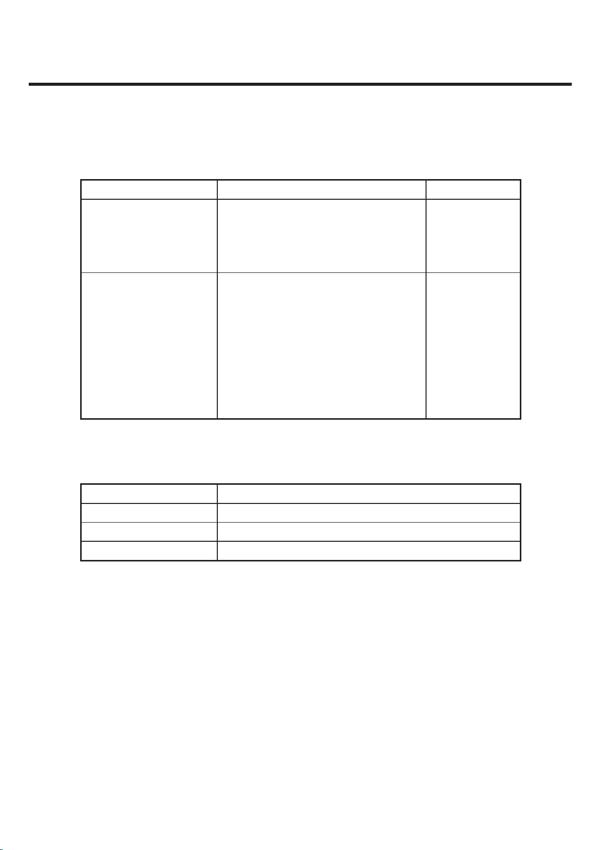
2.1 Supporting Standard
Item Feature Comment
Supporting Standard
WCDMA1900 / WCDMA850
GSM850/GSM900/DCS1800/PCS1900
Frequency Range
GSM850 TX : 824 – 849 MHz
GSM850 RX : 869 – 894 MHz
GSM900 TX : 880 – 915 MHz
GSM900 RX : 925 – 960 MHz
DCS1800 TX : 1710 – 1784 MHz
DCS1800 RX : 1805 – 1880 MHz
PCS1900 TX : 1850 – 1910 MHz
PCS1900 RX : 1930 – 1990 MHz
2.2 Main Parts : Solution
Digital Baseband
Qualcomm QSC6270
Analog Baseband
Qualcomm QSC6270
RF Chip
Qualcomm QSC6270
2. PERFORMANCE
Copyright © 2010 LG Electronics. Inc. All right reserved.
Only for training and service purposes
- 9 -
LGE Internal Use Only
2. PERFORMANCE
GU295/GU292 Product Specification
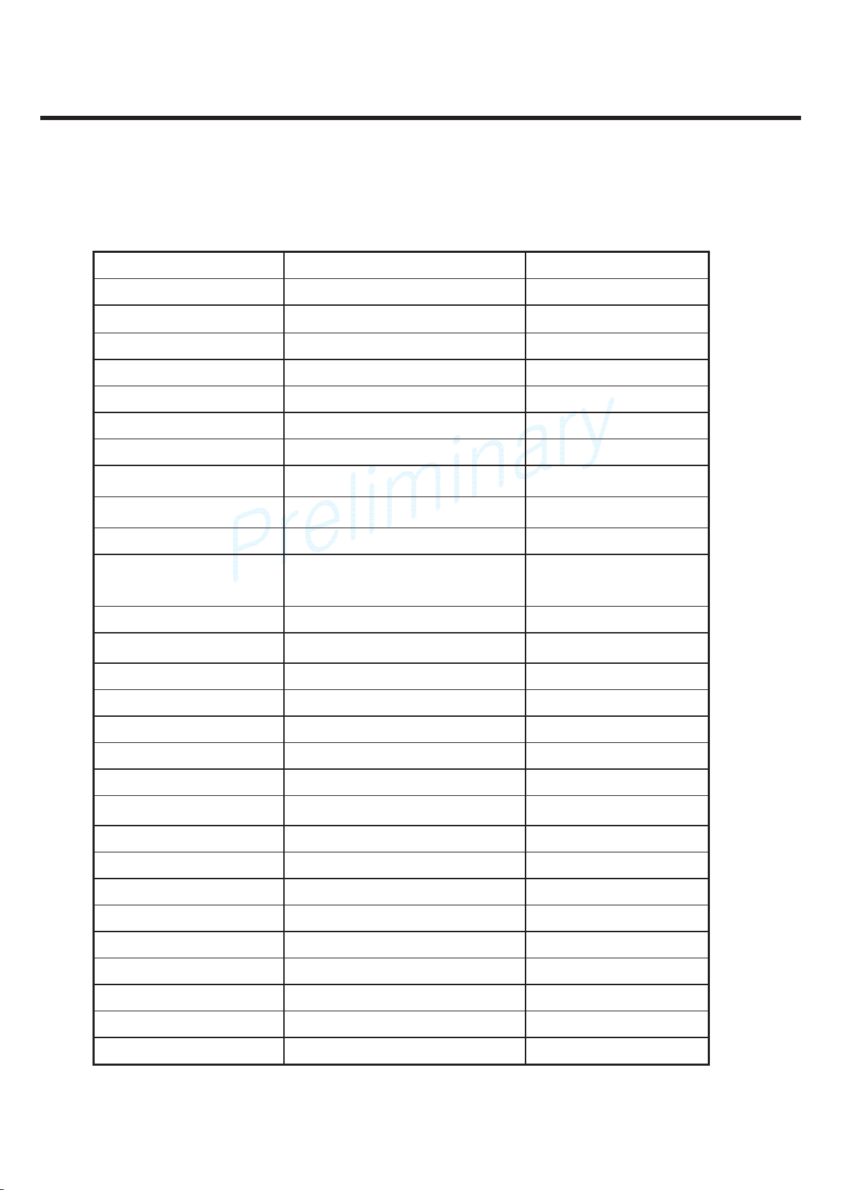
2.3 HW Features
Item Feature Comment
Form Factor
Slide
Battery
900mA,Li-Ion
Size
99.5 x 47 x 16.2mm
Weight
110g (include battery)
Volume
PCB
Rev 1.0
Stand by time
Over 250hrs @ Paging Period 5
Charging time
3hrs
Talk time
3hrs @Power Level 5(850/900)
RX sensitivity
-106dBm
TX output power
GSM850/900:32.5dBm,
DCS/PCS:29.5dBm
Class4(GSM),
Calss1(D/PCS)
SIM card type
1.8V or 3.0V
Display
2.0” 176 x 220
Keypad
Yes
ANT
Yes
System connector
Micro USB
Ear Phone Jack
Yes
PC synchronization
No Option
Memory
2G / 1G MB
Speech coding
Yes
Data & Fax
No
Vibrator
Yes
MIDI
64 Poly
Voice Recording
Yes
Speaker Phone
Yes
Travel Adapter
Yes
CDROM
No Option
Options
Yes
LGE Internal Use Only Copyright © 2010 LG Electronics. Inc. All right reserved.
- 10 -
Only for training and service purposes

GU295/GU292 Product Specification
2.4 SW Features
Item Feature Comment
RSSI
0 ~ 5 Levels
Battery Charging
0 ~ 3 Levels
Key Volume
0 ~ 7 Levels
Audio Volume
0 ~ 7 Levels
Time / Date Display
Yes
Multi-Language
Yes
Quick Access Mode
Yes
PC Sync
Yes
Speed Dial
Yes
CLIP / CLIR
Yes
Speaker Phone
Yes
Phone Book
Yes Max 1000
Last Dial Number
Yes
Last Received Number
Yes
Last Missed Number
Yes
Search by Number
/ Name
Partial Search by Name
Group
Yes
Fixed Dial Number
Yes
Service Dial Number
Yes
Own Number
Yes
Voice Memo
Yes
Call Reminder
No
Network Selection
Yes
Call Divert
Yes
Call Barring
Yes
Call Charge (AoC)
No
Call Duration
Yes
SMS
Yes
E-Mail
Yes
SMS Over GPRS
Yes
2. PERFORMANCE
0 ~ 7 Levels
Copyright © 2010 LG Electronics. Inc. All right reserved.
Only for training and service purposes
- 11 -
LGE Internal Use Only

2. PERFORMANCE
GU295/GU292 Product Specification
EMS Melody / Picture
Send / Receive / Save
Partial EMS Receive Only /
Save: Melody Only
Long Message
No
Cell Broadcast
Yes
Download
Yes
Game
Yes
Calendar
Yes
Memo Pad
Yes Support smart memo
World Clock
Yes
Unit Convert
Yes
Fax & Data
No
Wall Paper
Yes
WAP Browser
Yes
Download Melody /
Wallpaper
Yes
SIM Lock
Yes
SIM Toolkit
Yes
MMS
Yes
EONS
No
CPHS
Yes
Camera
Yes
JAVA
Yes
Voice Dial
No
IrDA
No
GPRS
Yes
Hold / Retrieve
Yes
Conference Call
Yes
DTMF
Yes
TTY
Yes
AMR
Yes
PTT(Push To Talk)
Yes
LGE Internal Use Only Copyright © 2010 LG Electronics. Inc. All right reserved.
No
- 12 -
Only for training and service purposes
GU295/GU292 Product Specification
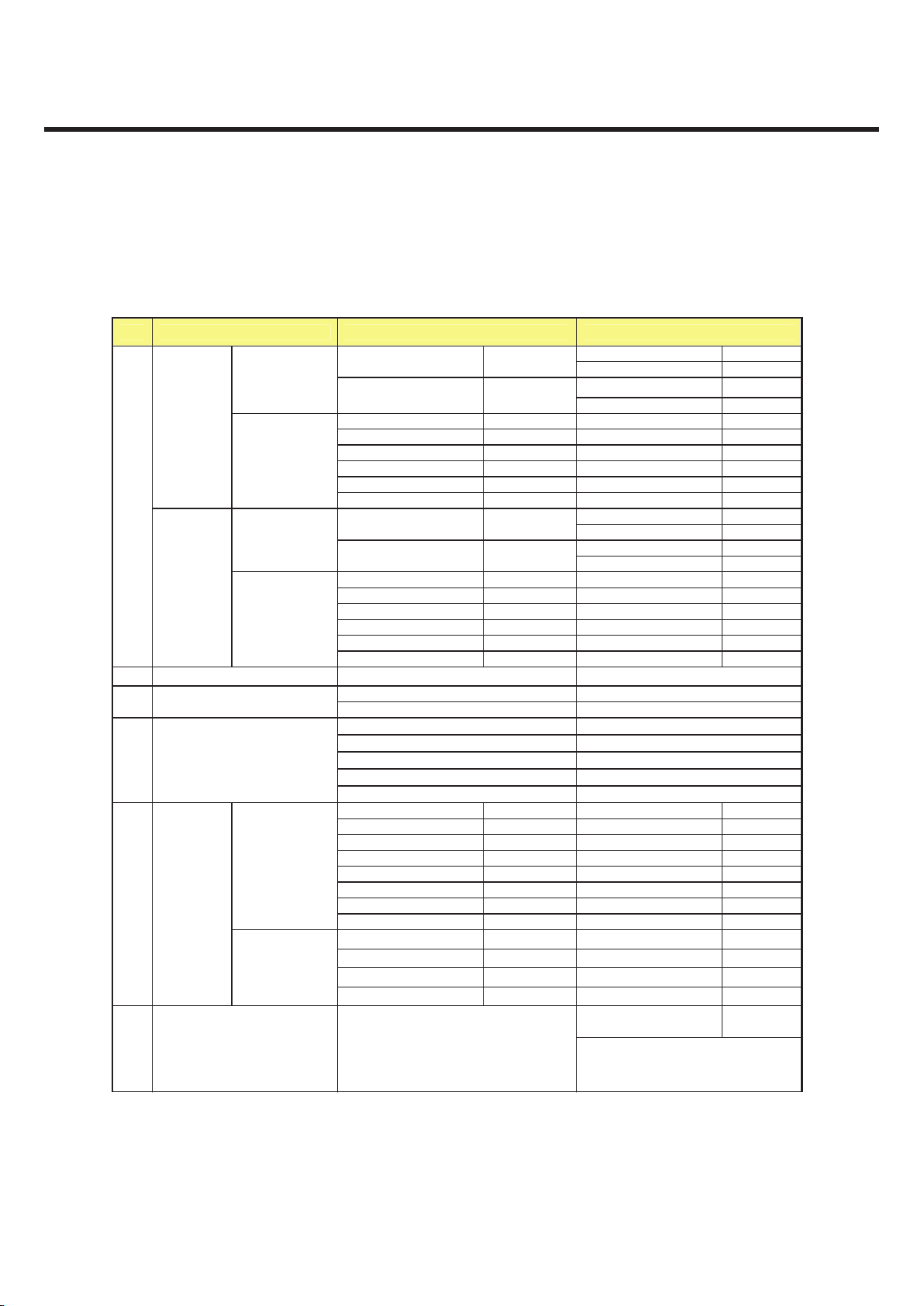
2.5 RF
2.5.1 RF Transmitter
GU295/GU292 Product Specification
NO Category GSM DCS/PCS
100kHz~1GHz
-36dBm
100kHz ~ 1GHz -36dBm
1G ~ 1710MHz
-30dBm
1.710GHz~1.785GHz
-36dBm
MS allocated
Channel
1GHz ~ 12.75GHz -30dBm
1.785GHz~12.75GHz
-30dBm
100kHz~880MHz
-57dBm
100kHz~880MHz
-57dBm
880MHz~915MHz
-59dBm
880MHz~915MHz
-59dBm
915MHz~1GHz
-57dBm
915MHz~1GHz
-57dBm
1GHz~1.710GHz
-47dBm
1GHz~1.710GHz
-47dBm
1.710GHz~1.785GHz
-53dBm
1.710GHz~1.785GHz
-53dBm
Conducte
d
Spurious
Emission
Idle Mode
1.785G~12.75GHz
-47dBm
1.785GHz~12.75GHz
-47dBm
30M ~ 1GHz
-36dBm
30M ~ 1GHz -36dBm
1GHz ~ 1710MHz
-30dBm
1710MHz~1785MHz
-36dBm
MS allocated
Channel
1G ~ 4GHz -30dBm
1785MHz~4GHz
-30dBm
30M ~ 880MHz -57dBm 30M ~ 880MHz -57dBm
880M ~ 915MHz -59dBm 880M ~ 915MHz -59dBm
915M ~ 1GHz -57dBm 915M ~ 1GHz -57dBm
1G ~ 1710MHz -47dBm 1G ~ 1710MHz -47dBm
1710M~1785MHz -53dBm 1710M~1785MHz -53dBm
1
Radiated
Spurious
Emission
Idle Mode
1785M ~ 4GHz -47dBm 1785M ~ 4GHz -47dBm
2 Frequency Error
< 0.1 ppm < 0.1 ppm
RMS < 5 degrees RMS < 5 degrees
3 Phase Error
Peak < 20 degrees Peak < 20 degrees
3dB below reference sensitivity 3dB below reference
RA250: 300Hzଝ RA130: ଝଝଝ0Hz
HT100: 0Hzଝଝଝ HT100: 3ଝ 50Hz
TU50: 0Hzଝଝଝ TU50: 2ଝ 60Hz
4
Frequency Error Under
Multipath and Interference
Condition
TU3: 0Hzଝଝଝ TU1,5: 3ଝ 20Hz
100kHz +0.5dB 100kHz +0.5dB
200kHz -30dB 200kHz -30dB
250kHz -33dB 250kHz -33dB
400kHz -60dB 400kHz -60dB
600~<1,800kHz -60dB 600~<1,800kHz -60dB
1,800~<3,000kHz -63dB 1,800~<3,000kHz -65dB
3,000~<6,000kHz -65dB 3,000~<6,000kHz -65dB
Due to
modulation
>6,000kHz -71dB >6,000kHz -73dB
400kHz -19dB 400kHz -22dB
600kHz -21dB 600kHz -24dB
1200kHz -21dB 1200kHz -24dB
5
Output RF
Spectrum
Due to
Switching
transient
1600kHz -24dB 1600kHz -27dB
Frequency offset 800kHz
7
Intermodulation
attenuation
Intermodulation product should
be Less than 55dB below the level
of Wanted signal
2. PERFORMANCE
Copyright © 2010 LG Electronics. Inc. All right reserved.
Only for training and service purposes
- 13 -
LGE Internal Use Only
2. PERFORMANCE
GU295/GU292 Product Specification
Po
wer
con
trol
Lev
el
Power
(dBm)
Tolerance
(dB)
Power
control
Level
Power
(dBm)
Tolerance
(dB)
5 33 ±2dB
0 30
±2dB
6 31 ±3dB
1 28
±3dB
7 29 ±3dB
2 26
±3dB
8 27 ±3dB
3 24
±3dB
9 25 ±3dB
4 22
±3dB
10 23 ±3dB
5 20
±3dB
11 21 ±3dB
6 18
±3dB
12 19 ±3dB
7 16
±3dB
13 17 ±3dB
8 14
±3dB
14 15 ±3dB
9 12
±4dB
15 13 ±3dB
10 10
±4dB
16 11 ±5dB
11 8
±4dB
17 9 ±5dB
12 6
±4dB
18 7 ±5dB
13 4
±4dB
19 5 ±5dB
14 2
±5dB
8
Transmitter Output Power
15 0
±5dB
9 Burst timing Mask IN Mask IN
LGE Internal Use Only Copyright © 2010 LG Electronics. Inc. All right reserved.
- 14 -
Only for training and service purposes
GU295/GU292 Product Specification
2.5.2 RF Receiver
NO Category GSM DCS
1 Sensitivity (TCH/FS Class II) -102dBm -100dBm
2
Co-Channel Rejection
(TCH/FS Class II,
RBER, TUhigh/FH)
C/Ic= 7dB C/Ic= 7dB
200kHz C/Ia1= -12dB C/Ia1= -12dB
3
Adjacent
Channel
Rejection
(Speech
Channel)
400kHz C/Ia2= -44dB C/Ia2= -44dB
Wanted Signal: -98dBm Wanted Signal: -96dBm
1’st interferer: -44dBm 1’st interferer: -44dBm
4 Intermodulation Rejection
2’nd interferer: -45dBm 2’nd interferer: -44dBm
5
Blocking Response
(TCH/FS Class II, RBER)
Wanted Signal: -101dBm
Unwanted Signal: Depend on
freq.
Wanted Signal: -101dBm
Unwanted Signal:
Depend on freq.
z All uncommented feature shall support GSM 11.10 and GCF(GSM Certification Forum)
2. PERFORMANCE
Copyright © 2010 LG Electronics. Inc. All right reserved.
Only for training and service purposes
- 15 -
LGE Internal Use Only
2. PERFORMANCE
GU295/GU292 Product Specification
2.5.3 HSDPA Transmitter Specification
Item Specification
Transmit Frequency Band1 : 1920 MHz ~ 1980 MHz
Band5 : 824 MHz ~ 849 MHz
Maximum Output
Power
Sub-Test
1=1/15, 2=12/15 21~25dBm / 3.84 MHz
3=13/15 4=15/8 20~25dBm / 3.84 MHz
5=15/7 6=15/0 19~25dBm / 3.84 MHz
HS-DPCCH
Sub-test
in table
C.10.1.4
Power
step
Power step slot
boundary
Power
step size,
P [dB]
Transmitter power step tolerance
[dB]
1 Start of
Ack/Nack
6 +/- 2.3
2 Start of CQI 1 +/- 0.6
3 Middle of CQI 0 +/- 0.6
5
4 End of CQI 5 +/- 2.3
Spectrum Emission
Mask
Sub-Test : 1=1/15, 2=12/15, 3=13/15, 4=15/8, 5=15/7, 6=15/0
Frequency offset
from carrier ᇞf
Minimum requirement Measurement Bandwidth
2.5 ~ 3.5 MHz -35-15×(ᇞf-2.5)dBc 30 kHz
3.5 ~ 7.5 MHz -35-1×(ᇞf-3.5)dBc 1 MHz
7.5 ~ 8.5 MHz -35-10×(ᇞf-7.5)dBc 1 MHz
8.5 ~ 12.5 MHz -49dBc 1 MHz
Adjacent Channel
Leakage
Power Ratio (ACLR)
Sub-Test : 1=1/15, 2=12/15, 3=13/15, 4=15/8, 5=15/7, 6=15/0
> 33 dB @ ±5 MHz
> 43 dB @ ±10 MHz
Error Vector
Magnitude
< 17.5 %, when Pout ≥ -20 dBm
Band2 : 1850 MHz ~ 1910 MHz
LGE Internal Use Only Copyright © 2010 LG Electronics. Inc. All right reserved.
- 16 -
Only for training and service purposes
- 17 -
Copyright © 2010 LG Electronics. Inc. All right reserved.
Only for training and service purposes
LGE Internal Use Only
2. PERFORMANCE
GU295/GU292 Product Specification
2.5.4 HSDPA Receiver Specification
Item Specification
Receive Frequency
Band1 : 2110 ~ 2170 MHz
Band8 : 925 ~ 960Hz
Maximum Input Level
(BLER or R), 16QAM Only
Sub-Test : 1=1/15, 2=12/15, 3=13/15, 4=15/8, 5=15/7, 6=15/0
BLER < 10% or R >= 700kbps
2.5.5 GPS Receiver Specification
Item Specification
Receive Frequency 1574.42 MHz ~ 1576.42 MHz
Minimum Sensitivity 1 satellite ≥-142dBm, 7 satellites ≥ -147dBm at coarse time aiding
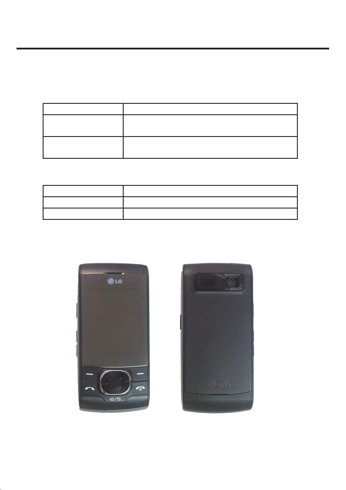
2.6 GU295 Figures
Band2 : 1930 ~ 1990 MHz
GU290v
3. TECHNICAL BRIEF
GU295
3. RF Technical Description
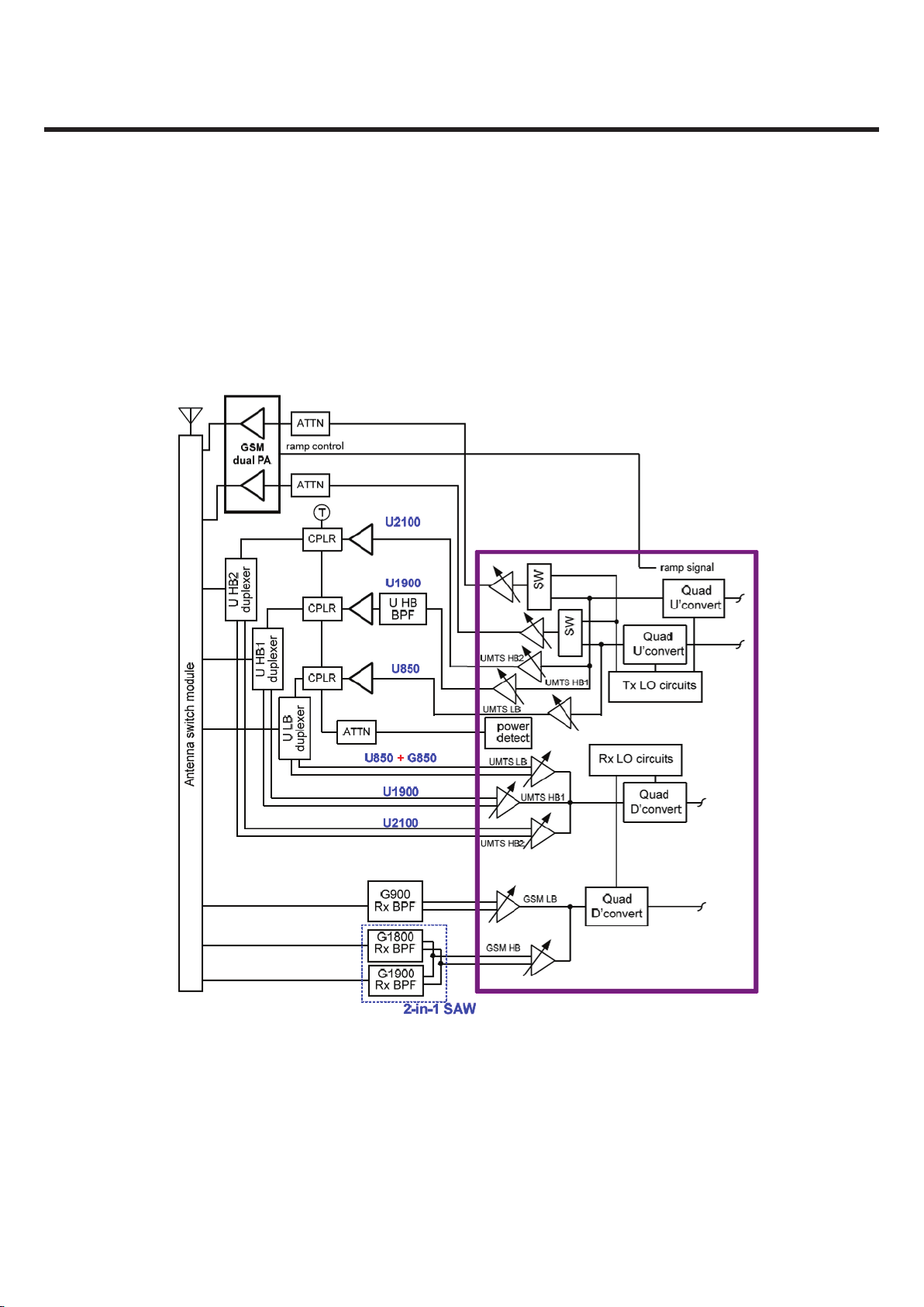
3.1 RF Technical Description
The RF platform of GU295 supports two different communication modes (WCDMA/GSM modes) including five
communication bands (W2100/W850/GSM850/GSM900/GSM1800/GSM1900).
The all the RF blocks can be divided into three main parts, which are a WCDMA part, a GSM, and a Antenna
switch module.
The simplified block diagram is shown in Figure 3.1.1
Figure 3.1.1 Block diagram of RF part
3. TECHNICAL BRIEF
GU290v
LGE Internal Use Only Copyright © 2010 LG Electronics. Inc. All right reserved.
- 18 -
Only for training and service purposes
3. TECHNICAL BRIEF
GU295
3.2 WCDMA Part
The W-CDMA transceiver uses differential analog in-phase and quadrature-phase interfaces, that is an IQ
interface, both in the receiver and transmitter information path.
The transceiver has the following general features:
. Power class : Power class 3 (+24dBm) in Band II and V
. Zero-IF Receiver.No IF filter needed
. Direct IQ modulation transmitter
Figure 3.2.1. WCDMA RF structure
Copyright © 2010 LG Electronics. Inc. All right reserved.
Only for training and service purposes
- 19 -
LGE Internal Use Only

3. TECHNICAL BRIEF
GU295
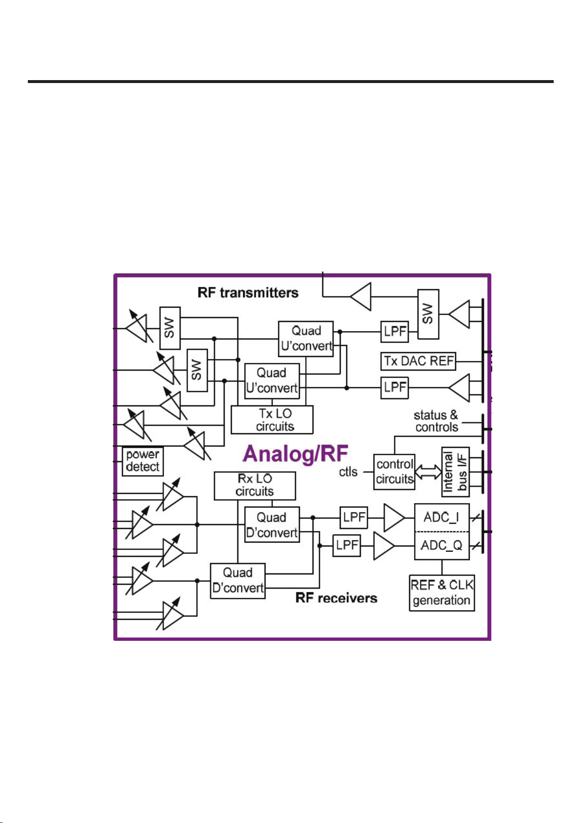
3.2.1 Transmitter Part
WCDMA Transmitter Block
The QSC62x0 device supports tri-band UMTS transmissions with three separate driver amplifier outputs; in
fact, most Tx active circuits are contained within the device. All three UMTS transmit paths (Figure 3.2.1.1)
begin with a single, shared analog baseband signal from the device’s baseband circuits. The baseband signal
is composed of two differential lines, one in-phase component and one quadrature-phase component. Each
component is lowpass filtered and amplified to levels sufficient for driving the quadrature upconverters.
There are two upconverters — one for low-band signals and one for high band — but only one upconverter is
active at a time.
Figure 3.2.1.1 WCDMA Transceiver Architecture
LGE Internal Use Only Copyright © 2010 LG Electronics. Inc. All right reserved.
- 20 -
Only for training and service purposes

3. TECHNICAL BRIEF
GU295
The active upconverter’s output is at the desired RF channel frequency and drives the QSC output stages.
These RF circuits include multiple variable-gain stages that provide transmit AGC control.
A greater than 81 dB gain control range is realized using information from the on-chip Tx power detector
combined with a control signal from the baseband circuits. The wide range of driver amplifier output levels is
achieved while supporting the WCDMA standard’s requirements for ACLR, spurious emissions, Rx-band noise,
etc.
The high-band driver amplifier output is followed by a SPDT switch that provides two high-band outputs,
thereby fulfilling the tri-band UMTS requirement. The low-band output port is driven directly by its output
amplifier.
All three output ports are single-ended with 50ohm nominal impedance. Each requires a matching network to
interface with its band-pass filter.
Each of the three UMTS Tx output chains are functionally identical: the QSC Tx output drives the PA through
the band-pass filter and a matching network; a directional coupler provides a sample of the PA output signal;
the through path of the coupler is routed to the Tx port of the duplexer; the duplexer antenna port is
connected to the antenna switch; and the switch is connected to the antenna.
The coupler outputs provide a low-level sample of the active transmitter’s Tx power. An on-chip powerdetector circuit provides a Tx power estimate that assists in setting the transmit gains and helps ensure that
the maximum allowed output power is not exceeded. The three UMTS couplers (one for each band) use a
daisy-chain configuration that allows them to share the single, on-chip power detector circuit.
Copyright © 2010 LG Electronics. Inc. All right reserved.
Only for training and service purposes
- 21 -
LGE Internal Use Only
3. TECHNICAL BRIEF
GU295
3.2.2 Receiver Part
WCDMA Receiver
The antenna collects the base station forward-link signal and radiates the phone’s reverse-link signal. In the
example of a multiband, multimode phone (Figure 3.2.2.1), a switch routes the antenna signals to one of the
three UMTS Rx/Tx paths, each beginning with its own band-specific duplexer that separates that band’s
receive and transmit paths
Figure 3.2.2.1 WCDMA Receiver schematic
LGE Internal Use Only Copyright © 2010 LG Electronics. Inc. All right reserved.
- 22 -
Only for training and service purposes

3. TECHNICAL BRIEF
GU295
Each UMTS duplexer provides a differential output signal that is compatible with its QSC LNA input.
The duplexer-to-LNA interface requires a differential matching network (MN) that optimizes the power
transfer into the LNA.
Although there are three UMTS LNAs, only one is active at a time. The active gain-stepped LNA output drives a
shared quadrature downconverter directly — an off-chip inter-stage filter is not required. The elimination of
this filter is achieved by a combination of factors:
- New on-chip QSC processing
- Higher performance achieved by the differential duplexer-to-LNA interface
- Greater duplexer suppression of Tx leakage
The downconverter’s RF circuitry includes another gain-stepped amplifier that supplements the LNA gain
steps to further extend the receiver dynamic range. The downconverter translates the active LNA’s RF signal
directly to baseband, producing two analog outputs: in-phase (I) and quadrature (Q). The UMTS baseband
signals are routed to lowpass filters whose passband and stopband characteristics are optimized for the active
WCDMA waveform. Both filter outputs are buffered to drive their analog-to-digital converters for digitization.
The digital baseband outputs are routed to QSC baseband circuits for further processing.
Copyright © 2010 LG Electronics. Inc. All right reserved.
Only for training and service purposes
- 23 -
LGE Internal Use Only
3. TECHNICAL BRIEF
GU295
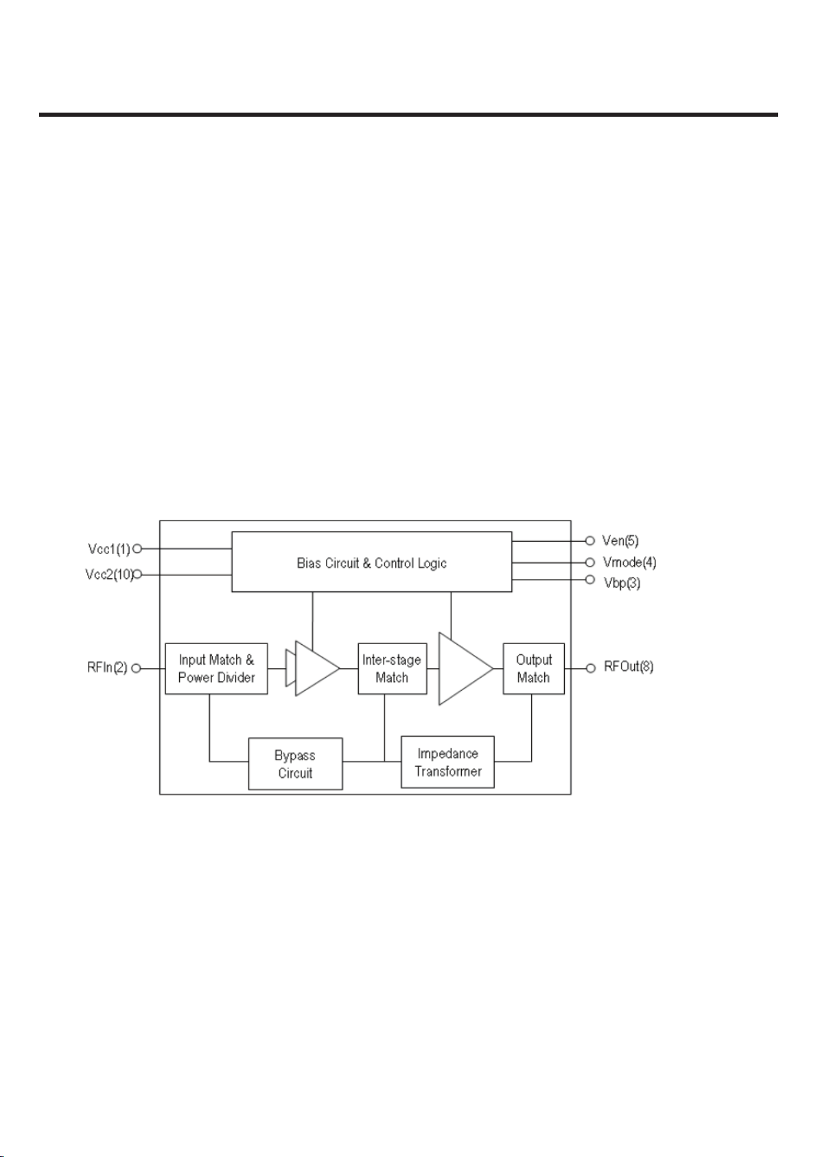
3.2.3 Power Amplifier Module
The ACPM-5202 is a fully matched 10-pin surface mount module developed for UMTS Band II.
This power amplifier module operates in the 1850-1910MHz bandwidth.
The ACPM-5202 meets stringent UMTS linearity requirements up to 28dBm output power.
The 3mmx3mm form factor package is self contained, incorporating 50ohm input and output matching
Networks The ACPM-5202 features 5th generation of CoolPAM circuit technology which supports 3 power
modes
– bypass, mid and high power modes. The CoolPAM is stage bypass technology enhancing PAE (power added
efficiency) at low and medium power range. Active bypass feature is added to 5th generation to enhance PAE
further at low output range. This helps to extend talk time. A directional coupler is integrated into the module
and both coupling and isolation ports are available externally, supporting daisy chain.
The power amplifier is manufactured on an advanced InGaP HBT (hetero-junction Bipolar Transistor)
MMIC (microwave monolithic integrated circuit) technology offering state-of-the-artreliability, temperature
stability and ruggedness.
Figure 3.2.3.1 ACPM-5202 Functional Block Diagram
LGE Internal Use Only Copyright © 2010 LG Electronics. Inc. All right reserved.
- 24 -
Only for training and service purposes
3. TECHNICAL BRIEF
DNI
R145
C199 8.2p
1950 MHz,2140 MHz
FL102
95
74
1
2
8
36
ANT TX_IN
RX_OUT2
GND1
RX_OUT1
GND2 GND4
GND3 GND5
FL106
1880,1960MHz
79
25
4
8
1
36
ANT TX_IN
RX_OUT1
RX_OUT2
GND1
GND2 GND4
GND3 GND5
1880MHz
FL105
5 3 2
4 1
INOUT
G1G2G3
C165 33p
C131 DNI
C160 3.3p
5.6pC145
4.7nL120
10n
C114
10pC127
6.8n
L130
L117
DNI
C143
DNI
68
R116
4.7n
L105
L121 3.3p
L125
33K
15pC130
C128
DNI
011R
001
001
9
01
R
C113
DNI
C142
1n
1n
C141
1n
C140
836.5MHz
FL104
5 3 2
4 1
INOUT
G1G2G3
C136
1n
L107
DNI
DNI
L111
3.9pC164
L112
DNI
C133 DNI
C132
4.7p
DNI
L108
1nC122
680p
C185
680p
C184
+VPWR+VPWR
C182
330p
C134 DNI
+VPWR
836.5 MHz,881.5 MHz
FL103
95
7
3
1
2
8
4
6
ANT
GND2
RX_OUT2
GND1
RX_OUT1
TX_IN
GND4
GND3 GND5
C129 DNI
L124
DNI
33pC163
15n
C121
4.7nL119
U103
6 5
7 4
8 3
9 2
10 1
11
PGND
VCC1VCC2
RFINRFOUT
VBPISO
VMODEGND
VENCPL
DNI
C126
C125
DNI
2.2u
C183
2.7nL118
1n
C124
1n
C123
330p
C181
+VPWR
6.8n
C151
0.5p
C161
6.8nL104
3.9n
L123
C162
10p
U102
6 5
7 4
8 3
9 2
10 1
11
PGND
VENCPL
VMODEGND
VBPISO
RFINRFOUT
VCC1VCC2
R103
49.9
8.2n
L122
0.5p
L106
2.2u
C180
C159
10p
PWR_DET
PA_R1
PA_R1
PA_R0
PA_R0
WCDMA_PA_ON0
WLNA_HB2_IN_M
WLNA_HB2_IN_P
WLNA_LB_IN_P
WLNA_LB_IN_M
WCDMA_2100_TX_OUT
WCDMA_900_TX_OUT
WLNA_HB1_IN_M
WLNA_HB1_IN_P
WCDMA_PA_ON1
WCDMA_1900_TX_OUT
WCDMA_2100
WCDMA_LB
WCDMA_1900
W2100
W1900
U103
ACPM-5202
ACPM-5201
W2100
W1900
FL105
B9414
B9640
W850
W900
FL104
B9442
B9425
WCDMA
WCDMA_1900
W900
W850
U102
ACPM-5308
Rev 1.0 ( Band II + V )
WCDMA_2100
ACPM-5305
W
CDMA_850/900
GU295
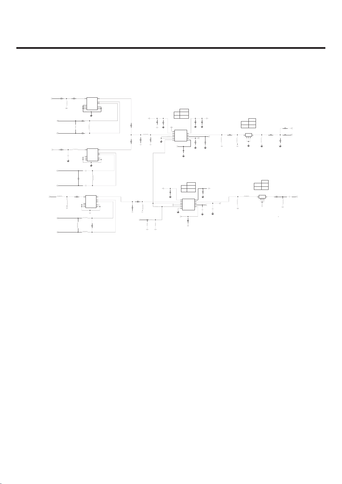
Figure 3.2.3.2 WCDMA PAM schematic
Copyright © 2010 LG Electronics. Inc. All right reserved.
Only for training and service purposes
- 25 -
LGE Internal Use Only

3. TECHNICAL BRIEF
GU295
3.3 EDGE/GPRS/GSM RF block
The EDGE/GPRS/GSM transceiver use a digital interface that is shared between receive and transmit data.
The receive interface is based on I and Q data and the transmitter interface is based on envelop and frequency
data.
The quad band EDGE/GSM/GPRS transceiver has the following general features:
Power class
GMSK low bands: Class 4 (33 dBm)
GMSK high bands: Class 1 (30 dBm)
8PSK low bands: Class E2 (27 dBm)
8PSK high bands: Class E2 (26 dBm)
Multi slot class 12 (4+4=5)
Dual Transfer Mode (DTM) class 9 (3+2=5)
Zero-IF receiver
-Polar modulation transmitter
3.3.1 Transmitter Part
GSM/EDGE Transmitter Block
The QSC62x0 device supports quad-band GSM transmissions with two separate dual-band driver amplifier
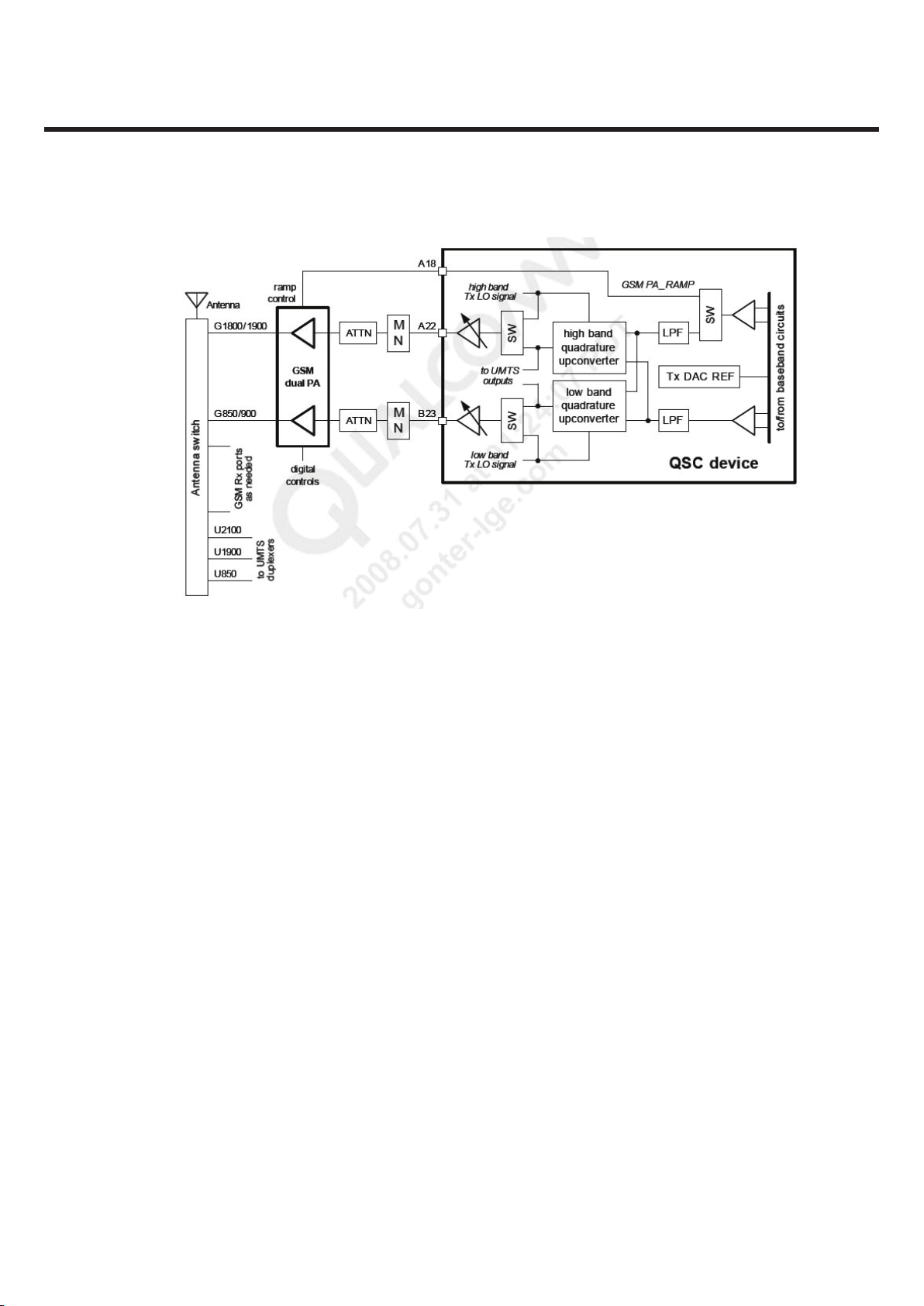
outputs; in fact, most Tx active circuits are contained within the device. Both GSM transmit paths (Figure 3.3.1.1)
begin with a single, shared analog baseband signal from the device’s baseband circuits — the same interface
and baseband circuits used by the UMTS transmitters. The GSM transmitters use the same quadrature
upconverters as well — one for low band signals and one for high band — with just one active at a time. The
transmitter LO signals are generated by circuits described in next section and delivered to the upconverter
circuits at the correct frequency, with the proper phase relationship, and with an adequate drive level.
The SPDT switches at each driver amplifier input allow selection of the output signal: either the actual GSM
signal from the upconverter or a test signal generated by the Tx LO synthesizer. The Tx output chain is
functionally identical for both the low band and the high band: the power amplifier is driven by the QSC device
through a matching network and a resistive attenuator; the PA output is routed to the antenna switch module
whose output is connected to the antenna.
In addition to the through signal path, the QSC device also provides the PA ramp control signal that ensures
smooth transitions while the transmitter is turned on and off for GSM’s burst transmissions.
The ramp signal is generated by one of the baseband circuit’s Tx DACs. A switch after the baseband amplifier
selects whether the DAC output signal is routed to GSM PA module for ramping the PA up or down, or to the
transmitter signal path for data transmission.
LGE Internal Use Only Copyright © 2010 LG Electronics. Inc. All right reserved.
- 26 -
Only for training and service purposes
3. TECHNICAL BRIEF
GU295
Figure 3.3.1.1 QSC GSM transmitter signal paths functional diagram
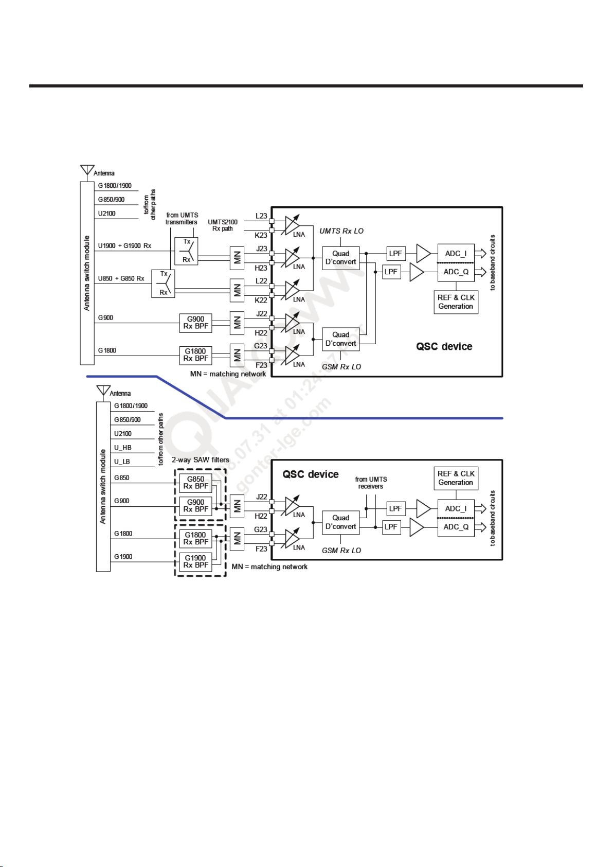
3.3.2 Receiver Part
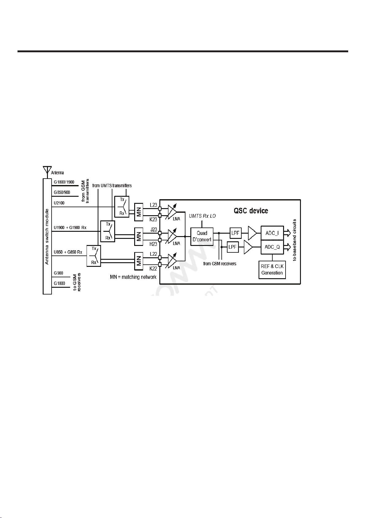
There are two recommended GSM receiver path configurations; both are shown in Figure 3.3.2.1.
The configuration shown on top allows the GSM 850 and GSM 1900 bands to share the UMTS 850 and UMTS
1900 paths
for US applications and uses four LNA inputs to support quad-band GSM operation.
The lower example uses two LNAs for quad-band GSM operation (one low band and one high band),
with two-way SAW filters between the antenna switch and the QSC inputs for each band type.
Copyright © 2010 LG Electronics. Inc. All right reserved.
Only for training and service purposes
- 27 -
LGE Internal Use Only
3. TECHNICAL BRIEF
GU295
Figure 3.3.2.1 QSC GSM receiver signal paths functional diagram
LGE Internal Use Only Copyright © 2010 LG Electronics. Inc. All right reserved.
- 28 -
Only for training and service purposes

3. TECHNICAL BRIEF
GU295
Shared UMTS/GSM configuration (four GSM LNAs)
In this configuration, the GSM 850 receive path shares the UMTS 850 receiver front-end path (including LNA).
Beginning at the antenna switch output, the GSM signal is routed through the UMTS850 duplexer to the shared
LNA input at pins L22 and K22. Likewise, the GSM 1900 receive path shares the UMTS 1900 front-end, including
pins J23 and H23.
The GSM 900 and GSM 1800 bands have dedicated receive paths from the antenna switch outputs to the QSC
LNA inputs.
Each band has its own band-select filter that drives its LNA input. All four GSM bands include input filtering:
the 850 and 1900 bands share the UMTS duplexer filtering, while the 900 and 1800 bands have dedicated
bandpass filters.
The filter functions suppress out-of-band received signals and the handset’s GSM transmitter leakage.
Transmit power suppression must be adequate to avoid overdriving the GSM Rx chain. Like the UMTS paths,
the GSM paths use a differential configuration into their LNAs, and thus equire differential matching networks.
The internal GSM receivers are functionally identical to the UMTS receivers: although there are multiple GSM
LNAs, only one is active at a time. The active gain-stepped LNA output drives a shared quadrature
downconverter directly — an off-chip inter-stage filter is not required. The elimination of this filter is achieved
by a combination of factors:
New on-chip QSC processing
Higher performance achieved by the differential duplexer-to-LNA interface
Greater duplexer suppression of Tx leakage
The downconverter’s RF circuitry includes another gain-stepped amplifier that supplements the LNA gain steps
to further extend the receiver dynamic range. The downconverter translates the active LNA’s RF signal directly
to baseband, producing two analog outputs: in-phase (I) and quadrature (Q). The GSM baseband signals drive
lowpass filters whose passband and stopband characteristics are optimized for the active GSM waveform. Both
filter outputs are buffered to drive their analog-to-digital converters for digitization. The digital baseband
outputs are routed to QSC baseband circuits for further processing.
The Rx LO signal is delivered to the downconverter circuits from the LO generation and distribution circuits as
described in next section.
Dedicated GSM configuration (two GSM LNAs)
In this configuration, the GSM 850 and GSM 1900 bands do not pass through the UMTS duplexers.
Instead, the two GSM LNA inputs are shared: the GSM 850 and GSM 900 bands share the low-band GSM LNA,
and the GSM 1800 and GSM 1900 bands share the high-band LNA.
Four switch module outputs are required, each driving its own GSM Rx path. A two-way SAW filter takes the
two low-band (or high-band) single-ended inputs from the antenna switch and provides one filtered,
differential output that drives the appropriate QSC LNA input.
Beyond the LNA inputs, this GSM receiver configuration is identical to the paths described earlier for the shared
UMTS/GSM configuration.
Copyright © 2010 LG Electronics. Inc. All right reserved.
Only for training and service purposes
- 29 -
LGE Internal Use Only

3. TECHNICAL BRIEF
GU295
3.3.3 Rx LO circuits
The QSC62x0 device integrates all of the frequency synthesizer functions that generate the UMTS and GSM
receive LO signals (UHF local oscillator, PLL circuits, and loop filter), plus the distribution circuits that deliver the
quadrature LO signals to the two downconverters.
The buffered 19.2 MHz TCXO or XO signal provides the synthesizer input (REF), the frequency reference to
which the PLL is phase and frequency locked. The reference is divided to create a fixed frequency input to the
phase detector, FR.
The other phase detector input (FV) varies as the loop acquires a lock and is generated by dividing the local
oscillator output frequency using the feedback path’s counter. The closed-loop will force FV to equal FR when
locked.
If the loop is not locked, the error between FV and FR will create an error signal. This error signal is filtered by
the loop filter and applied to the local oscillator, tuning the output frequency so that the error is decreased.
Ultimately the loop forces the error to approach zero and the PLL is phase and frequency locked.
LGE Internal Use Only Copyright © 2010 LG Electronics. Inc. All right reserved.
- 30 -
Only for training and service purposes
GU295
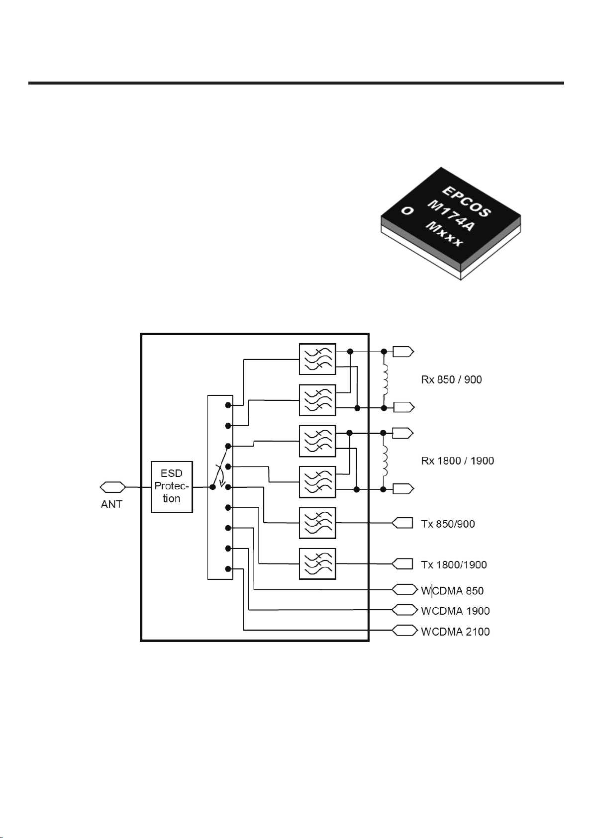
3.3.4 Front-End Module (FEM)
Low-loss SAW frontend module for mobile telephone system
Covering GSM850, GSM900, GSM1800, GSM1900,
3 ports for WCDMA or TD-SCDMA
Integration of TX low pass filters, switches and decoder
Integration of GSM 850, EGSM, PCN and PCS RX SAWs
Balanced outputs of all RX ports, diplexed for GSM850 / EGSM
and PCN / PCS
Integration of ESD protection at Ant port to 8kV
acc. IEC-61000-4-2 (contact discharge)
Figure 3.3.4.1 Block diagram of FEM
3. TECHNICAL BRIEF
Copyright © 2010 LG Electronics. Inc. All right reserved.
Only for training and service purposes
- 31 -
LGE Internal Use Only
 Loading...