

LG GU280, GU285 Service Manual

Service Manual Model : GU280/GU285
Internal Use Only
Service Manual
GU280/GU285
Date: October, 2009 / Issue 1.0

Table Of Contents
1. INTRODUCTION ...............................................5
1.1 Purpose ......................................................................5
1.2 Regulatory Information .................................................5
2. PERFORMANCE ...............................................7
2.1 Product Name .............................................................7
2.2 Supporting Standard ....................................................7
2.3 Main Parts : Solution ....................................................7
2.4 Feature .......................................................................8
2.5 HW Spec. ..................................................................10
3. Technical Brief ............................................. 13
3.1. General Description ..................................................13
3.2. WCDMA Part ............................................................14
3.3. EDGE/GPRS/GSM RF block ........................................19
3.5. Control Flow .............................................................24
3.6 General Description ...................................................25
3.7 Power management ..................................................35
4. TROUBLE SHOOTING ..................................... 38
4.1 RF Component ..........................................................38
4.2 RF Path ....................................................................39
4.3 Trouble Shooting of GSM Part (GSM850/900/1800/1900)
......................................................................................40
4.4 Trouble Shooting of WCDMA Part ................................48
4.5 Checking Bluetooth Block ..........................................55
4.6 Checking FM Radio Block ..........................................58
4.7 Base band part ..........................................................61
4.8 Charger Troubleshooting ............................................63
4.9 USB Troubleshooting ..................................................64
4.10 USIM Detect Troubleshooting ....................................66
4.11 Camera Troubleshooting ..........................................68
4.12 Main Keypad Backlight Troubleshooting ....................70
4.13 Sub Keypad Backlight Troubleshooting ......................71
4.14 LCD Troubleshooting ................................................73
4.15 Vibrator ...................................................................74
4.16 Receiver Path ..........................................................75
4.17 Headset path...........................................................77
4.18 Speaker phone path ................................................79
4.19 Main microphone ....................................................81
4.20 Headset microphone ................................................83
5. Downloading ................................................ 85
5.1 Introduction ...............................................................85
5.2 Downloading Procedure .............................................86
5.3 Troubleshooting Download Errors ..............................101
5.4 Caution ...................................................................106
6. Block Diagram ........................................... 107
7. CIRCUIT DIAGRAM ...................................... 109
8. BGA Pin Map .............................................. 117
9. PCB LAYOUT ...............................................121
10. CALIBRATION ............................................127
10.1 Confi guration of directory .......................................127
10.2 How to use Tachyon ...............................................129
11. EXPLODED VIEW & REPLACEMENT
PART LIST ................................................ 131
11.1 EXPLODED VIEW ...................................................131
11.2 Replacement Parts ................................................133
11.3 Accessory ............................................................. 150
Copyright © 2009 LG Electronics. Inc. All right reserved.
Only for training and service purposes
- 3 -
LGE Internal Use Only

LGE Internal Use Only Copyright © 2009 LG Electronics. Inc. All right reserved.
- 4 -
Only for training and service purposes

1. INTRODUCTION
BL20
1. INTRODUCTION
1.1. Purpose
This manual provides the information necessary to repair, calibration, description and download the
features of this model.
1.2. Regulatory Information
A. Security
Toll fraud, the unauthorized use of telecommunications system by an unauthorized part (for example,
persons other than your company’s employees, agents, subcontractors, or person working on your
company’s behalf) can result in substantial additional charges for your telecommunications services.
System users are responsible for the security of own system.
There are may be risks of toll fraud associated with your telecommunications system. System users
are responsible for programming and configuring the equipment to prevent unauthorized use. The
manufacturer does not warrant that this product is immune from the above case but will prevent
unauthorized use of common carrier telecommunication service of facilities accessed through or
connected to it. The manufacturer will not be responsible for any charges that result from such
unauthorized use.
B. Incidence of Harm
If a telephone company determines that the equipment provided to customer is faulty and possibly
causing harm or interruption in service to the telephone network, it should disconnect telephone
service until repair can be done. A telephone company may temporarily disconnect service as long as
repair is not done.
C. Changes in Service
A local telephone company may make changes in its communications facilities or procedure. If these
changes could reasonably be expected to affect the use of the phones or compatibility with the net
work, the telephone company is required to give advanced written notice to the user, allowing the user
to take appropriate steps to maintain telephone service.
D. Maintenance Limitations
Maintenance limitations on the phones must be performed only by the manufacturer or its authorized
agent. The user may not make any changes and/or repairs expect as specifically noted in this manual.
Therefore, note that unauthorized alternations or repair may affect the regulatory status of the system
and may void any remaining warranty.
E. Notice of Radiated Emissions
This model complies with rules regarding radiation and radio frequency emission as defined by local
regulatory agencies. In accordance with these agencies, you may be required to provide information
such as the following to the end user.
Copyright © 2009 LG Electronics. Inc. All right reserved.
Only for training and service purposes
- 5 -
LGE Internal Use Only

1. INTRODUCTION
BL20
F. Pictures
The pictures in this manual are for illustrative purposes only; your actual hardware may look slightly
different.
G. Interference and Attenuation
A phone may interfere with sensitive laboratory equipment, medical equipment, etc. Interference from
unsuppressed engines or electric motors may cause problems.
H. Electrostatic Sensitive Devices
ATTENTION
Boards, which contain Electrostatic Sensitive Device (ESD), are indicated by the sign. Following
information is ESD handling:
• Service personnel should ground themselves by using a wrist strap when exchange system boards.
• When repairs are made to a system board, they should spread the floor with anti-static mat which is
also grounded.
• Use a suitable, grounded soldering iron.
• Keep sensitive parts in these protective packages until these are used.
• When returning system boards or parts like EEPROM to the factory, use the protective package as
described.
LGE Internal Use Only Copyright © 2009 LG Electronics. Inc. All right reserved.
- 6 -
Only for training and service purposes

2. PERFORMANCE
2.1 Product Name
GU280 : WCDMA2100+EGSM/GSM850/DCS/PCS
(GPRS Class 12 / EDGE Class 12)
2.2 Supporting Standard
2. PERFORMANCE
CommentFeatureItem
Supporting Standard
Frequency Range
WCDMA(FDD1)/EGSM/GSM850/DCS1800/PCS1900
with seamless handover
Phase 2+(include AMR)
SIM Toolkit : Class 1, 2, 3, C-E
WCDMA(FDD1) TX : 1920 – 1980 MHz
WCDMA(FDD1) RX : 2110 – 2170 MHz
EGSM TX : 880 – 915 MHz
EGSM RX : 925 – 960 MHz
GSM850 TX : 824 – 849 MHz
GSM850 RX : 869 – 894 MHz
DCS1800 TX : 1710 – 1785 MHz
DCS1800 RX : 1805 – 1880 MHz
PCS1900 TX : 1850 – 1910 MHz
PCS1900 RX : 1930 – 1990 MHz
WAP 2.0, JAVA(MIDP 2.1 CLDC 1.1)Application Standard
2.3 Main Parts : Solution
QSC6240 : QualcommDigital Baseband
QSC6240 : QualcommAnalog Baseband
QSC6240 : QualcommRF Chip
Copyright © 2009 LG Electronics. Inc. All right reserved.
Only for training and service purposes
- 7 -
CommentPart NameItem
QSC6240 is an one-chip
solution(DB + AB + RF +
PM)
LGE Internal Use Only
2. PERFORMANCE
2.4 Feature
CommentFeatureItem
Slide typeForm Factor
Battery
Size
Stand by time
Talk time
RX sensitivity
1) Capacity
Standard : Li-Ion, 900mAh
2) Packing Type : Inner Pack
Standard :
96.0 x 45.7 x 14.9mm
TBDVolume
Staggered 10 Layers , 0.8tPCB
2G : Over 320 hrs
3G : Over 250 hrs
2G : Over 180mins
3G : Over 180 mins
WCDMA(FDD1) < -105 dBm
EGSM < -105 dBm
GSM850 < -105 dBm
DCS 1800 < -105 dBm
PCS 1900 <-105 dBm
With Battery115gWeight
@ Paging Period 5 (2G)
@ DRX 1.28 (3G)
@ Power Off / 900mAh3 hrsCharging time
@ Power Level 5 (2G)
@ Tx = 12dBm (3G)
TX output
power
LGE Internal Use Only Copyright © 2009 LG Electronics. Inc. All right reserved.
WCDMA/
GSM/
GPRS
EDGE
WCDMA : 24dBm/3.84MHz,+1/-3dBm
EGSM : 33dBm
GSM850 : 33 dBm
DCS 1800 : 30 dBm
PCS 1900 : 30 dBm
GSM 900 : 27 dBm
DCS 1800 : 26 dBm
PCS 1900 : 26 dBm
GPRS Class 12GPRS compatibility
EDGE Class 12EDGE compatibility
- 8 -
Class3(WCDMA)
Class4 (EGSM)
Class4 (GSM850)
Class1 (PCS)
Class1 (DCS)
E2 (GSM900)
E2 (PCS)
E2 (DCS)
Only for training and service purposes

2. PERFORMANCE
SIM card type
Display
Keypad
Memory
Plug-In SIM
3V /1.8V
Main LCD
TFT Main LCD(2’, 176 x 220)
1.3 CMOS Camera Built-in Camera
Slide Key pad : 11
Main Key pad : 15
Main : Internal Fixed TypeANT
5 PinSystem connector
3.5Phi, 4 Pole, StereoEar Phone Jack
YesPC synchronization
NAND Flash : 1Gbit
SDRAM : 512Gbit
FR, EFR, HR,AMRSpeech coding
Support
(External Memory)
NoData & Fax
Built in VibratorVibrator
EDR 2.0Blue Tooth
MP3/ WMA/AAC/HE-AAC/EAAC+Music Player
MPEG4, H.263, WMV9Video Player
MPEG4, H.263, Camcorder
YesVoice Recording
YesSpeaker Phone mode
YesTravel Adapter
NoCDROM
OptionStereo Headset
OptionData Cable
NoT-Flash
Copyright © 2009 LG Electronics. Inc. All right reserved.
Only for training and service purposes
- 9 -
LGE Internal Use Only

2. PERFORMANCE
2.5 HW Spec.
GSM Transmitter/Receiver spec.
Item Specification
Phase Error
Frequency Error
EMC(Radiated Spurious Emission
Disturbance)
Transmitter Output power and Burst
Timing
Burst Timing <3.69us
Spectrum due to modulation out to less
than 1800kHz offset
Spectrum due to modulation out to larger
than 1800kHz offset to the edge of the
transmit band
Rms : 5°
Peak : 20 °
GSM : 0.1 ppm
DCS/PCS : 0.1 ppm
GSM/DCS : < -28dBm
GSM : 5dBm – 33dBm ± 3dB
DCS/PCS : 0dBm – 30dBm ± 3dB
200kHz : -36dBm
600kHz : -51dBm/-56dBm
GSM :
1800-3000kHz :< -63dBc(-46dBm)
3000kHz-6000kHz : <-65dBc(-46dBm)
6000kHz < : < -71dBc(-46dBm)
DCS :
1800-3000kHz :< -65dBc(-51dBm)
6000kHz < : < -73dBc(-51dBm)
Spectrum due to switching transient
Reference Sensitivity – TCH/FS Class II(RBER) : -105dBm(2.439%)
Usable receiver input level range 0.012(-15 - -40dBm)
Intermodulation rejection – Speech
channels
AM Suppression
-GSM : -31dBm - DCS : -29dBm
Timing Advance ± 0.5T
LGE Internal Use Only Copyright © 2009 LG Electronics. Inc. All right reserved.
400kHz : -19dBm/-22dBm(5/0), -23dBm
600kHz : -21dBm/-24dBm(5/0), -26dBm
± 800kHz, ± 1600kHz
: -98dBm/-96dBm (2.439%)
-98dBm/-96dBm (2.439%)
- 10 -
Only for training and service purposes

WCDMA Transmitter spec.
Item Specification
2. PERFORMANCE
Transmit Frequency
Maximum Output Power
1920 MHz ~ 1980 MHz
+24 dBm / 3.84 MHz, +1 / -3 dB
Frequency Error within ±0.1 PPM
Open Loop Power
Control
Minimum Transmit Power
Occupied Bandwidth
Adjacent Channel
Leakage
Normal Conditions : within ±9 dB,
Extreme Conditions : within ±12 dB
< -50 dBm /3.84 MHz
< 5 MHz at 3.84 Mcps (99% of power)
> 33 dB @ ±5 MHz,
> 43 dB @ ±10 MHz
Power Ratio (ACLR)
Spurious Emissions
| > 12.5 MHz
|f-f
c
< -36 dBm / 1 kHz RW @ 9 kHz ≤ f < 150 kHz
< -36 dBm / 10 kHz RW @ 150 KHz ≤ f < 30 MHz
< -36 dBm / 100 kHz RW @ 30 MHz ≤ f < 1 GHz
< -30 dBm / 1 MHz RW @ 1 GHz ≤ f < 12.75 GHz
< -41 dBm / 300 kHz RW @ 1893.5 MHz < f < 1919.6 MHz
< -67 dBm / 100 kHz RW @ 925 MHz ≤ f ≤ 935 MHz
< -79 dBm / 100 kHz RW @ 935 MHz < f ≤ 960 GHz
< -71 dBm / 100 kHz RW @ 1805 MHz ≤ f ≤ 1880 MHz
Transmit Intermodulation < -31 dBc @ 5 MHz & < -41 dBc @ 10 MHz
when Interference CW Signal Level = -40 dBc
Error Vector Magnitude < 17.5 %, when Pout ≥ -20 dBm
Peak Code Domain Error
< -15 dB at Pout t -20 dBm
Copyright © 2009 LG Electronics. Inc. All right reserved.
Only for training and service purposes
- 11 -
LGE Internal Use Only

2. PERFORMANCE
WCDMA Receiver spec.
Item Specification
Receive Frequency 2110MHz ~ 2170 MHz
Reference Sensitivity Level BER < 0.001 when Î
Maximum Input Level BER < 0.001 when Î
Adjacent Channel Selectivity
(ACS)
ACS > 33 dB where BER < 0.001 when Î
= –52 dBm / 3.84 MHz @ ±5 MHz
& I
oac
Blocking Characteristic BER < 0.001 when Î
& I
or I
= -56 dBm / 3.84 MHz @ Fuw(offset) = ±10 MHz
blocking
= -44 dBm / 3.84 MHz @ Fuw(offset) = ±15 MHz
blocking
= -106.7 dBm / 3.84 MHz
or
= -25 dBm / 3.84 MHz
or
or
= -103.7 dBm / 3.84 MHz
or
= -92.7 dBm / 3.84 MHz
Spurious Response BER < 0.001 when Îor= -103.7 dBm / 3.84 MHz & I
Intermodulation BER < 0.001 when Î
& I
= -46 dBm @ F
ouw1
& I
= -46 dBm / 3.84 MHz @ F
ouw2
= -103.7 dBm / 3.84 MHz
or
(offset) = ±10 MHz
uw1
(offset) = ±20 MHz
uw2
Spurious Emissions < -57 dBm / 100 kHz BW @ 9 kHz ≤ f < 1 GHz
< -47 dBm / 1 MHz BW @ 1 GHz ≤ f ≤ 12.75 GHz
blocking
= -44 dBm
Adjust output(TPC command)
cmd 1dB 2dB 3dB
+1 +0.5/1.5 +1/3 +1.5/4
Inner Loop Power Control
In Uplink
0 -0.5/+0.5 -0.5/+0.5 -0.5/+0.5
-1 -0.5/-1.5 -1/-3 -1.5/-4
group(10equal command group)
+1 +8/+12 +16/+24
LGE Internal Use Only Copyright © 2009 LG Electronics. Inc. All right reserved.
- 12 -
Only for training and service purposes
3. Technical Brief
3.1. General Description
The RF platform of GU280 supports two different communication modes (WCDMA/GSM modes)
including five communication bands (W2100/W850/GSM850/GSM900/GSM1800/GSM1900).
The all the RF blocks can be divided into three main parts, which are a WCDMA part, a GSM, and
a Antenna switch module.
The simplified block diagram is shown in Figure 1.1.1
3. Technical Brief
Figure 1.1.1 Block diagram of RF part
Copyright © 2009 LG Electronics. Inc. All right reserved.
Only for training and service purposes
- 13 -
LGE Internal Use Only
3. Technical Brief
3.2. WCDMA Part
The W-CDMA transceiver uses differential analog in-phase and quadrature-phase interfaces,
that is an IQ-interface, both in the receiver and transmitter information path.
The transceiver has the following general features:
. Power class : Power class 3 (+24dBm) in Band II and V
. Zero-IF Receiver.No IF filter needed
. Direct IQ modulation transmitter
Figure 1.2.1. WCDMA RF structure
LGE Internal Use Only Copyright © 2009 LG Electronics. Inc. All right reserved.
- 14 -
Only for training and service purposes
3. Technical Brief
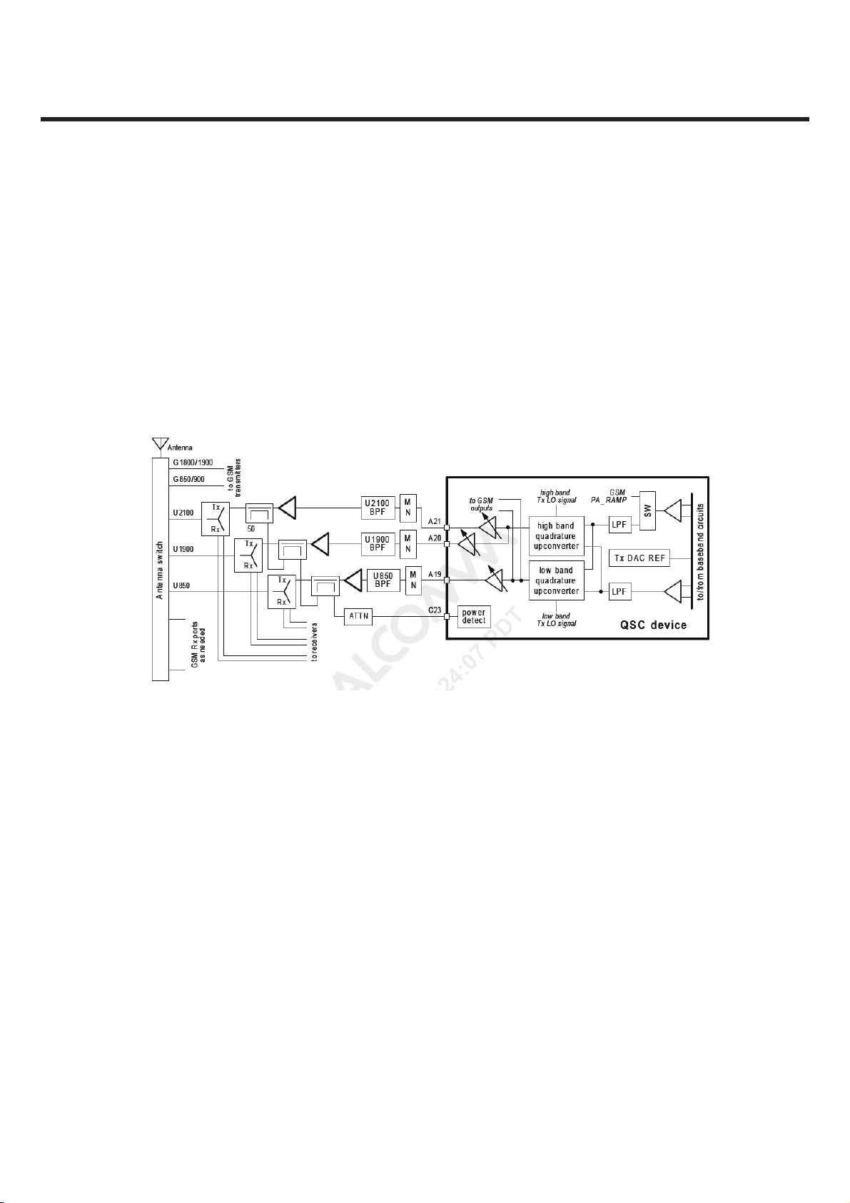
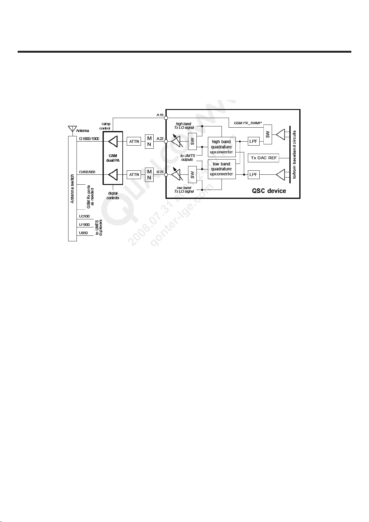
3.2.1. Transmitter Part
WCDMA Transmitter Block
The QSC62x0 device supports tri-band UMTS transmissions with three separate driver amplifier outputs; in fact,
most Tx active circuits are contained within the device. All three UMTS transmit paths (Figure 1.2.1.1) begin with a
single, shared analog baseband signal from the device’s baseband circuits. The baseband signal is composed of
two differential lines, one in-phase component and one quadrature-phase component. Each component is lowpass
filtered and amplified to levels sufficient for driving the quadrature upconverters. There are two upconverters —
one for low-band signals and one for high band — but only one upconverter is active at a time.
Figure 1.2.1.1 WCDMA Transceiver Architecture
The active upconverter’s output is at the desired RF channel frequency and drives the QSC output stages.
These RF circuits include multiple variable-gain stages that provide transmit AGC control.
A greater than 81 dB gain control range is realized using information from the on-chip Tx power detector combined
with a control signal from the baseband circuits. The wide range of driver amplifier output levels is achieved
while supporting the WCDMA standard’s requirements for ACLR, spurious emissions, Rx-band noise, etc.
The high-band driver amplifier output is followed by a SPDT switch that provides two high-band outputs,
thereby fulfilling the tri-band UMTS requirement. The low-band output port is driven directly by its output amplifier.
All three output ports are single-ended with 50ohm nominal impedance. Each requires a matching network to
interface with its band-pass filter.
Each of the three UMTS Tx output chains are functionally identical: the QSC Tx output drives the PA through
the band-pass filter and a matching network; a directional coupler provides a sample of the PA output signal;
the through path of the coupler is routed to the Tx port of the duplexer; the duplexer antenna port is connected to
the antenna switch; and the switch is connected to the antenna.
The coupler outputs provide a low-level sample of the active transmitter’s Tx power. An on-chip power-detector
circuit provides a Tx power estimate that assists in setting the transmit gains and helps ensure that the maximum
allowed output power is not exceeded. The three UMTS couplers (one for each band) use a daisy-chain configuration
that allows them to share the single, on-chip power detector circuit.
Copyright © 2009 LG Electronics. Inc. All right reserved.
Only for training and service purposes
- 15 -
LGE Internal Use Only

3. Technical Brief
3.2.2. Receiver Part
WCDMA Receiver
The antenna collects the base station forward-link signal and radiates the phone’s reverse-link signal. In the example of
a multiband, multimode phone (Figure 1.2.2.1), a switch routes the antenna signals to one of the three UMTS Rx/Tx paths,
each beginning with its own band-specific duplexer that separates that band’s receive and transmit paths
Figure 1.2.2.1 WCDMA Receiver schematic
Each UMTS duplexer provides a differential output signal that is compatible with its QSC LNA input.
The duplexer-to-LNA interface requires a differential matching network (MN) that optimizes the power transfer into
the LNA.
Although there are three UMTS LNAs, only one is active at a time. The active gain-stepped LNA output drives a
shared quadrature downconverter directly — an off-chip inter-stage filter is not required. The elimination of this
filter is achieved by a combination of factors:
- New on-chip QSC processing
- Higher performance achieved by the differential duplexer-to-LNA interface
-Greater duplexer suppression of Tx leakage
The downconverter’s RF circuitry includes another gain-stepped amplifier that supplements the LNA gain steps to
further extend the receiver dynamic range. The downconverter translates the active LNA’s RF signal directly to
baseband, producing two analog outputs: in-phase (I) and quadrature (Q). The UMTS baseband signals are routed
to lowpass filters whose passband and stopband characteristics are optimized for the active WCDMA waveform.
Both filter outputs are buffered to drive their analog-to-digital converters for digitization. The digital baseband
outputs are routed to QSC baseband circuits for further processing.
LGE Internal Use Only Copyright © 2009 LG Electronics. Inc. All right reserved.
- 16 -
Only for training and service purposes
3. Technical Brief
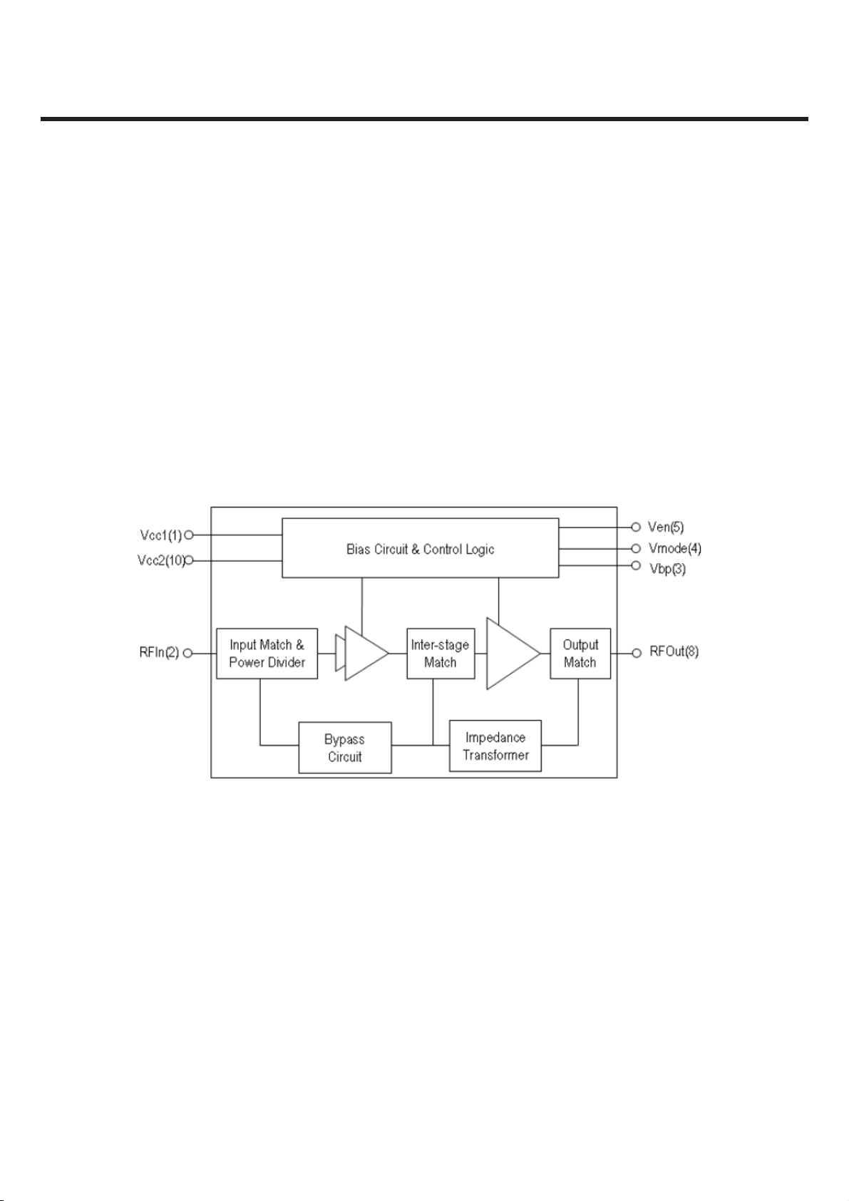
3.2.3. Power Amplifier Module
The ACPM-5201 is a fully matched 10-pin surface mount module developed for UMTS Band1.
This power amplifier module operates in the 1920-1980MHz bandwidth.
The ACPM-5001 meets stringent UMTS linearity requirements up to 27.5dBm output power.
The 3mmx3mm form factor package is self contained, incorporating 50ohm input and output matching
Networks The ACPM-5201 features 5th generation of CoolPAM circuit technology which supports 3 power modes
– bypass, mid and high power modes. The CoolPAM is stage bypass technology enhancing PAE (power added
efficiency) at low and medium power range. Active bypass feature is added to 5th generation to enhance PAE
further at low output range. This helps to extend talk time. A directional coupler is integrated into the module and
both coupling and isolation ports are available externally, supporting daisy chain.
The power amplifier is manufactured on an advanced InGaP HBT (hetero-junction Bipolar Transistor)
MMIC (microwave monolithic integrated circuit) technology offering state-of-the-artreliability, temperature stability
and ruggedness.
Figure 1.2.3.1 ACPM-5201 Functional Block Diagram
Copyright © 2009 LG Electronics. Inc. All right reserved.
Only for training and service purposes
- 17 -
LGE Internal Use Only
3. Technical Brief
DNIL116
C149 DNI
2
1
WCDMA_1900
WCDMA_1900
WLNA_HB1_IN_M
WLNA_HB1_IN_P
4.7pL120
1
WCDMA_2100
WCDMA_2100
WCDMA_850/900
WLNA_HB2_IN_M
WLNA_HB2_IN_P
WCDMA_LB
1
2
L119
DNI
6.8nR111
WLNA_LB_IN_M
WLNA_LB_IN_P
1
2
2
2
C160
12n
1
B7686FL101
1
ANT TX_IN
2
1
RX_OUT1
C127
RX_OUT2
DNI
4
GND1
2
GND2 GND4
GND3 GND5
1880,1960MHz
2
1
L121
DNI
2
C138 2.2p
2
B7696
FL106
3.3nC144
1
ANT
TX_IN
2
RX_OUT1
RX_OUT2
2
GND1
GND2 GND4
GND3 GND5
1950 MHz,2140 MHz
1.8nC116
1
1
L115
1p
2
C142 1.8n
1
B7671FL103
8.2pC148
6
2
1
ANT
TX_IN
RX_OUT1
RX_OUT2
2
GND1
4
GND2
GND4
GND3 GND5
836.5 MHz,881.5 MHz
L108 33p
1
L107
10n
L109 33p
1
36
1
8
25
79
0
2
1
PCS_IN_M
C126
DNI C133
2.2pC134
1
1
2
1
L118
10n
2
DNI C129
1
1
2
0
2
1
PCS_IN_P
C123
36
1
8
74
95
2
1
L117
DNI
2
2
3
1
8
7
95
2
1
C124
0.5p
2
2
+VPWR
2
1
C173
DNI
2
1
1
C135
DNI
1
C143
2
33p
2
DNIL123
1
2
1
1
C132
DNI
2
2
PWR_DET
2
C151
C158
2.2u
330p
1
1
ACPM-5201 U102
11
PGND
10 1
1nC128
2
2
1
C159
DNI
2
2
C180
DNI
411R
0
1
R109
2
1
68
2
2
70
801R
001
001
1
R
1
1
VCC1VCC2
92
RFINRFOUT
R103
83
1
74
49.9
VMODEGND
65
WCDMA_PA_ON0
C139
1n
2
C146
680p
1
WCDMA_PA_ON1
VBPISO
VENCPL
2
1
65
74
83
92
10 1
11
+VPWR
2
2
C130
C147
2.2u
330p
1
1
1.5nC119
1
PA_R1
PA_R0
2
C140
1n
1
VCC1VCC2
RFINRFOUT
VBPISO
VMODEGND
VENCPL
PGND
U104ACPM-5305
2
C136
DNI
1
2
2
C155
1n
L125
DNI
1
1
+VPWR+VPWR
2
C145
680p
1
PA_R0
2
2
C156
C137
DNI
DNI
1
1
B9414FL104
41
OUT
2
1
2
PA_R1
IN
G1G2G3
532
1950MHz
C141
DNI
L110 DNI
1
2
L111
DNI
1
2
2.7nC118
2
1
C150
4.7n
2
FL102
B9425
41
IN
OUT
G1G2G3
532
836.5MHz
1
2
L122
0.5p
1
DNIC181
2
C117 33p
2
2
1
L124
DNI
2
WCDMA_1900
1
WCDMA_1900_TX_OUT
1
WCDMA_2100_TX_OUT
WCDMA_2100
DNIC125
1
WCDMA_900_TX_OUT
WCDMA_850/900
Figure 1.2.3.2 WCDMA PAM schematic
LGE Internal Use Only Copyright © 2009 LG Electronics. Inc. All right reserved.
- 18 -
Only for training and service purposes

3. Technical Brief
3.3. EDGE/GPRS/GSM RF block
The EDGE/GPRS/GSM transceiver use a digital interface that is shared between receive and transmit data.
The receive interface is based on I and Q data and the transmitter interface is based on envelop and frequency data.
The quad band EDGE/GSM/GPRS transceiver has the following general features:
Power class
GMSK low bands: Class 4 (33 dBm)
GMSK high bands: Class 1 (30 dBm)
8PSK low bands: Class E2 (27 dBm)
8PSK high bands: Class E2 (26 dBm)
Multi slot class 12 (4+4=5)
Dual Transfer Mode (DTM) class 9 (3+2=5)
Zero-IF receiver
-Polar modulation transmitter
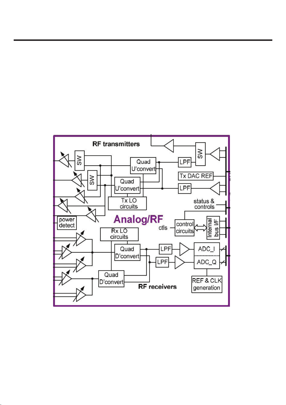
3.3.1. Transmitter Part
GSM/EDGE Transmitter Block
The QSC62x0 device supports quad-band GSM transmissions with two separate dual-band driver amplifier outputs; in
fact, most Tx active circuits are contained within the device. Both GSM transmit paths (Figure 1.3.1.1) begin with a
single, shared analog baseband signal from the device’s baseband circuits — the same interface and baseband
circuits used by the UMTS transmitters. The GSM transmitters use the same quadrature upconverters as well — one
for low band signals and one for high band — with just one active at a time. The transmitter LO signals are generated
by circuits described in next section and delivered to the upconverter circuits at the correct frequency, with the
proper phase relationship, and with an adequate drive level.
The SPDT switches at each driver amplifier input allow selection of the output signal: either the actual GSM signal
from the upconverter or a test signal generated by the Tx LO synthesizer. The Tx output chain is functionally identical
for both the low band and the high band: the power amplifier is driven by the QSC device through a matching
network and a resistive attenuator; the PA output is routed to the antenna switch module whose output is connected
to the antenna.
In addition to the through signal path, the QSC device also provides the PA ramp control signal that ensures smooth
transitions while the transmitter is turned on and off for GSM’s burst transmissions.
The ramp signal is generated by one of the baseband circuit’s Tx DACs. A switch after the baseband amplifier selects
whether the DAC output signal is routed to GSM PA module for ramping the PA up or down, or to the transmitter
signal path for data transmission.
Copyright © 2009 LG Electronics. Inc. All right reserved.
Only for training and service purposes
- 19 -
LGE Internal Use Only
3. Technical Brief
Figure 1.3.1.1 QSC GSM transmitter signal paths functional diagram
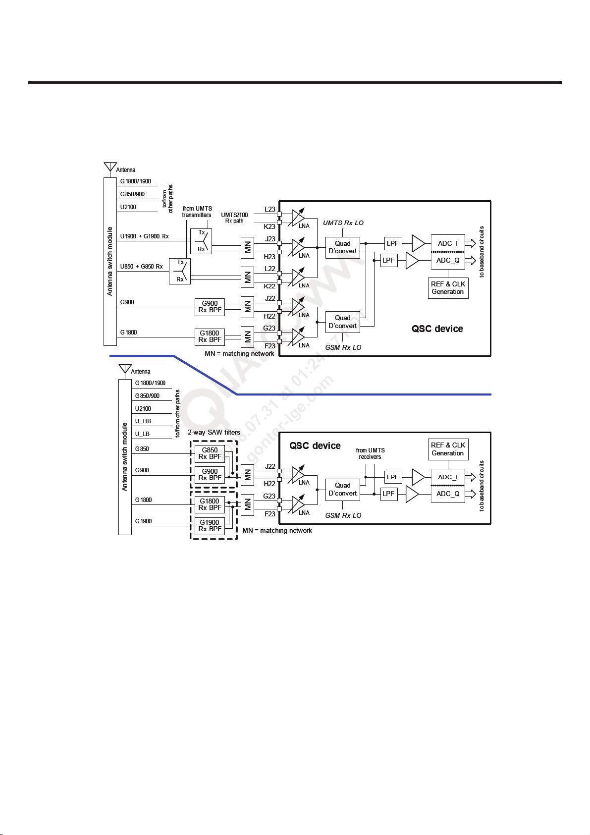
3.3.2. Receiver Part
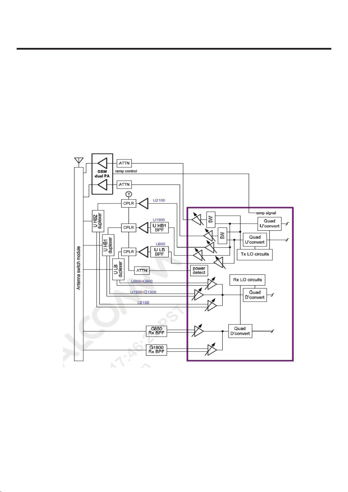
There are two recommended GSM receiver path configurations; both are shown in Figure 1.3.2.1.
The configuration shown on top allows the GSM 850 and GSM 1900 bands to share the UMTS 850 and UMTS 1900
paths for US applications and uses four LNA inputs to support quad-band GSM operation.
The lower example uses two LNAs for quad-band GSM operation (one low band and one high band),
with two-way SAW filters between the antenna switch and the QSC inputs for each band type.
LGE Internal Use Only Copyright © 2009 LG Electronics. Inc. All right reserved.
- 20 -
Only for training and service purposes
3. Technical Brief
Figure 1.3.2.1 QSC GSM receiver signal paths functional diagram
Copyright © 2009 LG Electronics. Inc. All right reserved.
Only for training and service purposes
- 21 -
LGE Internal Use Only

3. Technical Brief
Shared UMTS/GSM configuration (four GSM LNAs)
In this configuration, the GSM 850 receive path shares the UMTS 850 receiver front-end path (including LNA).
Beginning at the antenna switch output, the GSM signal is routed through the UMTS850 duplexer to the shared LNA
input at pins L22 and K22. Likewise, the GSM 1900 receive path shares the UMTS 1900 front-end, including pins J23 and
H23. The GSM 900 and GSM 1800 bands have dedicated receive paths from the antenna switch outputs to the QSC LNA
inputs. Each band has its own band-select filter that drives its LNA input. All four GSM bands include input filtering:
the 850 and 1900 bands share the UMTS duplexer filtering, while the 900 and 1800 bands have dedicated bandpass
filters. The filter functions suppress out-of-band received signals and the handset’s GSM transmitter leakage.
Transmit power suppression must be adequate to avoid overdriving the GSM Rx chain. Like the UMTS paths,
the GSM paths use a differential configuration into their LNAs, and thus equire differential matching networks.
The internal GSM receivers are functionally identical to the UMTS receivers: although there are multiple GSM LNAs,
only one is active at a time. The active gain-stepped LNA output drives a shared quadrature downconverter directly
— an off-chip inter-stage filter is not required. The elimination of this filter is achieved by a combination of factors:
New on-chip QSC processing
Higher performance achieved by the differential duplexer-to-LNA interface
Greater duplexer suppression of Tx leakage
The downconverter’s RF circuitry includes another gain-stepped amplifier that supplements the LNA gain steps
to further extend the receiver dynamic range. The downconverter translates the active LNA’s RF signal directly to
baseband,
producing two analog outputs: in-phase (I) and quadrature (Q). The GSM baseband signals drive lowpass filters whose
passband and stopband characteristics are optimized for the active GSM waveform. Both filter outputs are buffered
to drive their analog-to-digital converters for digitization. The digital baseband outputs are routed to QSC baseband
circuits for further processing. The Rx LO signal is delivered to the downconverter circuits from the LO generation and
distribution circuits as described in next section.
Dedicated GSM configuration (two GSM LNAs)
In this configuration, the GSM 850 and GSM 1900 bands do not pass through the UMTS duplexers.
Instead, the two GSM LNA inputs are shared: the GSM 850 and GSM 900 bands share the low-band GSM LNA,
and the GSM 1800 and GSM 1900 bands share the high-band LNA. Four switch module outputs are required, each
driving its own GSM Rx path. A two-way SAW filter takes the two low-band (or high-band) single-ended inputs from the
antenna switch and provides one filtered, differential output that drives the appropriate QSC LNA input.
Beyond the LNA inputs, this GSM receiver configuration is identical to the paths described earlier for the shared
UMTS/GSM configuration.
3.3.3. Rx LO circuits
The QSC62x0 device integrates all of the frequency synthesizer functions that generate the UMTS and GSM receive
LO signals (UHF local oscillator, PLL circuits, and loop filter), plus the distribution circuits that deliver the quadrature
LO signals to the two downconverters. The buffered 19.2 MHz TCXO or XO signal provides the synthesizer input (REF),
the frequency reference to which the PLL is phase and frequency locked. The reference is divided to create a fixed
frequency input to the phase detector, FR. The other phase detector input (FV) varies as the loop acquires a lock and is
generated by dividing the local oscillator output frequency using the feedback path’s counter. The closed-loop will
force FV to equal FR when locked. If the loop is not locked, the error between FV and FR will create an error signal. This
error signal is filtered by the loop filter and applied to the local oscillator, tuning the output frequency so that the error
is decreased. Ultimately the loop forces the error to approach zero and the PLL is phase and frequency locked.
LGE Internal Use Only Copyright © 2009 LG Electronics. Inc. All right reserved.
- 22 -
Only for training and service purposes
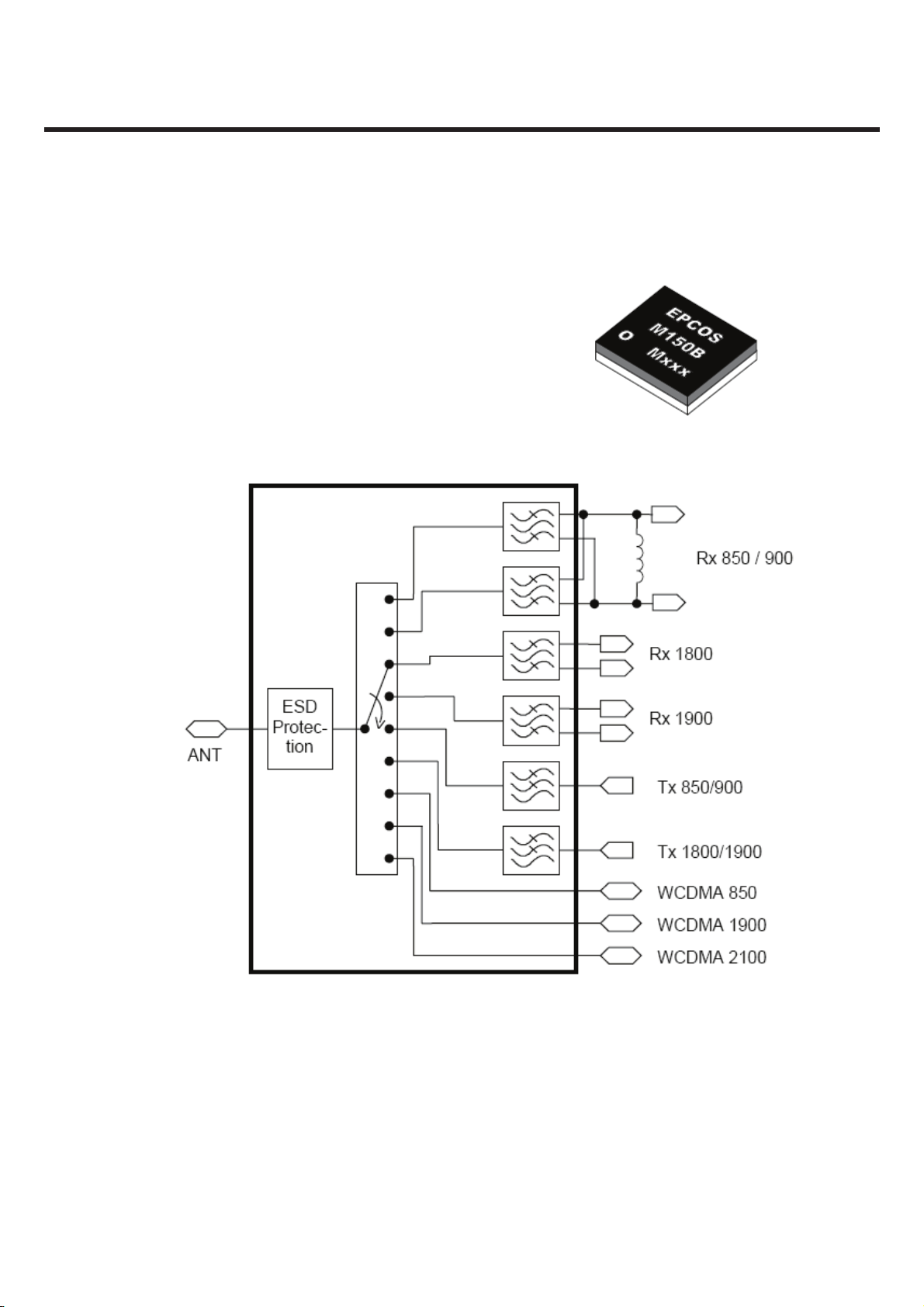
3.3.4. Front-End Module (FEM)
■ Low-loss SAW frontend module for mobile telephone system
■ Covering GSM850, GSM900, GSM1800, GSM1900,
WCDMA 2100 bands
■ Integration of TX low pass filters, switches and decoder
■ Integration of GSM 850, EGSM, PCN and PCS RX SAWs
■ Balanced outputs of all RX ports, diplexed for GSM 850/ EGSM
■ Integration of ESD protection at Ant port to 8kV
acc. IEC-61000-4-2 (contact discharge)
3. Technical Brief
Figure 1.3.4.1 Block diagram of FEM
Copyright © 2009 LG Electronics. Inc. All right reserved.
Only for training and service purposes
- 23 -
LGE Internal Use Only
3. Technical Brief
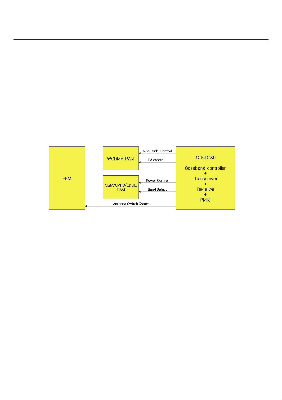
3.5. Control Flow
The access side of the digital baseband controller controls the overall radio system. In both EDGE/GSM/GPRS
and W-CDMA air interface mode, the digital baseband controller controls the radio system through a serial bus.
The digital baseband controller also manages PA band control and the antenna switch mechanism in the front end
module. The 26 MHz VCXO clock residing in the GSM/EDGE transceiver is turned on only when required, the digital
baseband controller initiates this.
The EDGE/GSM/GPRS RF system requires control, which is temperature dependent.
The temperature within the RF system is estimated by a voltage measurement performed by the analog baseband
controller. The control flow for the RF system is shown in Figure 1.5.1.
Figure 1.5.1 Block diagram of FEM
LGE Internal Use Only Copyright © 2009 LG Electronics. Inc. All right reserved.
- 24 -
Only for training and service purposes
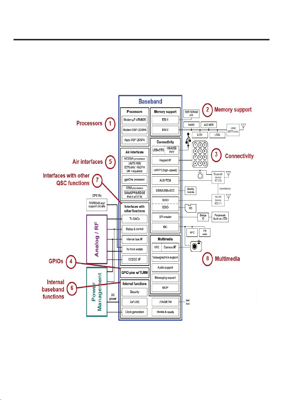
3. Base Band Technical Description
3.6 General Description
QSC6240 has all eight major functional blocks as like Figure 2.1
3. Technical Brief
Figure 2.1 QSC6240 Base band block
Copyright © 2009 LG Electronics. Inc. All right reserved.
Only for training and service purposes
- 25 -
LGE Internal Use Only
3. Technical Brief
3.6.1 Processor
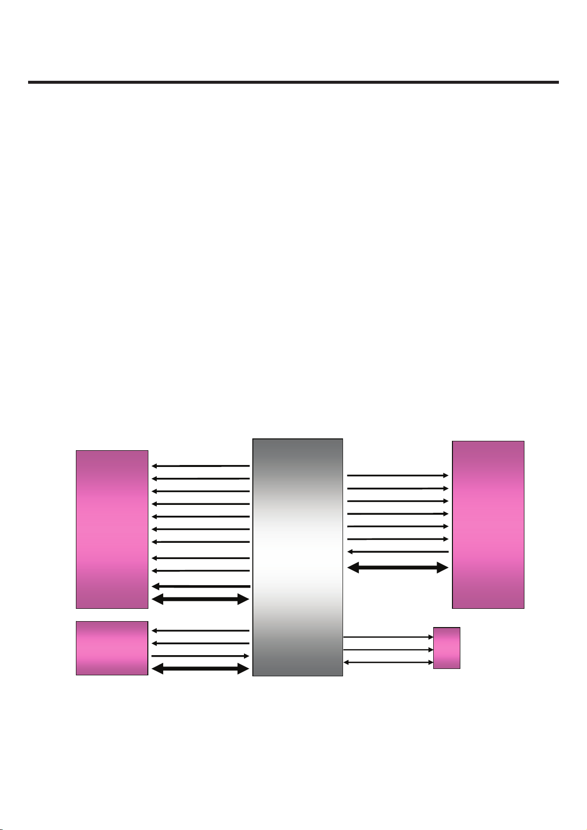
The QSC6240 device integrates multiple processors on-chip: one ARM microprocessor and two
DSP processors. Each processor is part of a functional subsystem:
The micro subsystem includes the ARM926EJ-S microprocessor.
The modem subsystem includes the QDSP4u8 digital signal processor (mDSP).
The application subsystem includes the QDSP4u8 application digital signal processor(aDSP).
Figure 2.1.1 Processors and bus architecture
LGE Internal Use Only Copyright © 2009 LG Electronics. Inc. All right reserved.
- 26 -
Only for training and service purposes
3. Technical Brief
R
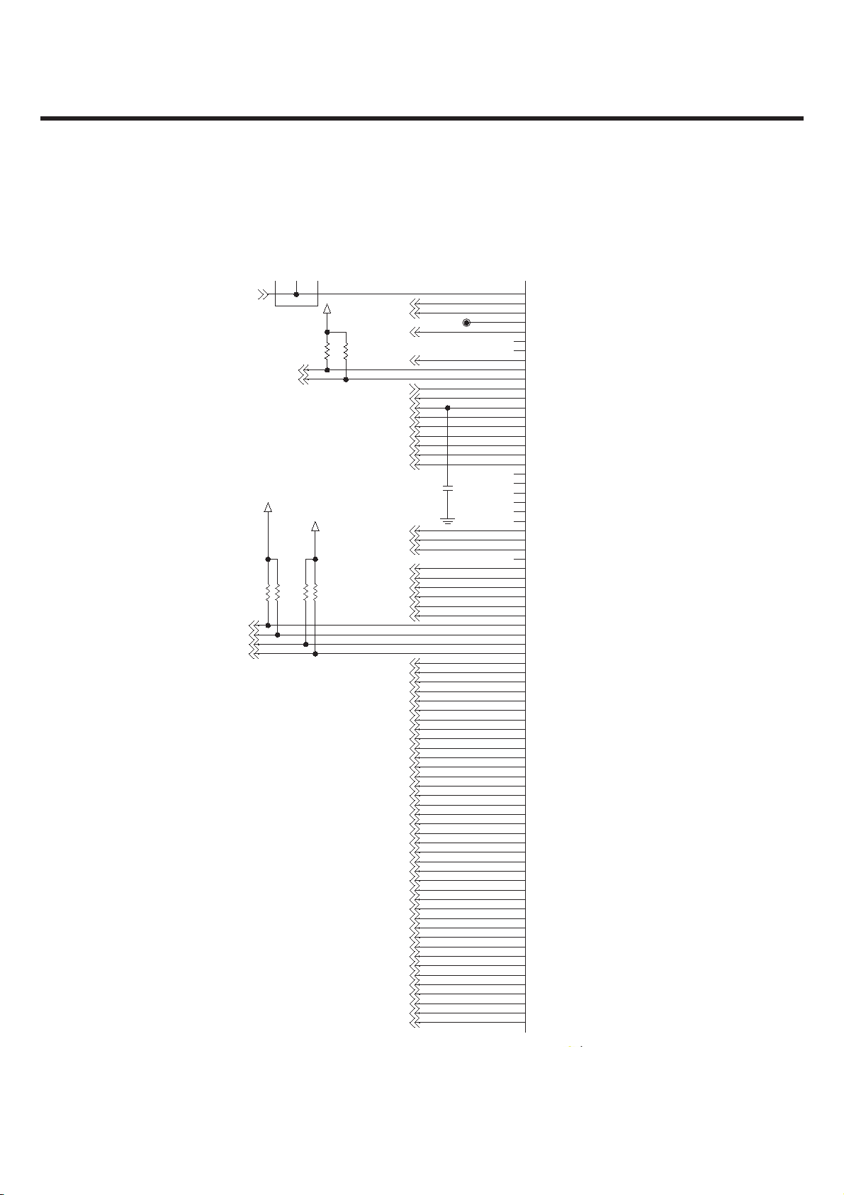
3.6.2 Memory support (and LCD interface)
The QSC62x0 device has two external bus interface (EBI) ports: EBI1 and EBI2.
EBI1 supports high-speed synchronous dynamic devices. Its memory controller supports the new
mobile DDR SDRAM memories with its higher bandwidth and ability to run at high clock
frequencies. This interface supports the high-bandwidth, high-density, and low-latency
requirements of the QSC’s advanced on-chip capabilities such as the ARM9 processor, highperformance
graphics, and video applications.
EBI2 is the slower speed interface intended to support memory devices such as NAND flash and
asynchronous SRAM, peripheral devices such as LCDs, and the UBM receiver for multicast or
broadcast reception (QSC6270 only). In addition, EBI2 is required to support a synchronous-burst
AAD NOR flash to enable a NOR/DDR SDRAM memory configuration because the simultaneous
mode (NOR, SDRAM) is not supported on the EBI1 bus.
The ARM926EJ-S microprocessor is a cached processor and all its accesses to external memory
use burst techniques of four or eight 32-bit words when the memory region is declared to be
cacheable/bufferable. To take advantage of this QSC higher performance feature, data from
memories must satisfy the requirements for these burst accesses.
DDR
SDRAM
DDR
512Mbit
SDRAM
512Mbit
External Memory (MICRO-
External Memory (MICRO-
SD card)
SD card)
EBI1 EBI2
EBI1 EBI2
SDRAM_CKE
SDRAM_CLK_P
SDRAM_CKE
SDRAM_CLK_N
SDRAM_CLK_P
SDRAM_CS_N
SDRAM_CLK_N
SDRAM_CS_N
SDRAM_WE_N
SDRAM_WE_N
SDRAM_RAS_N
SDRAM_RAS_N
SDRAM_CAS_N
SDRAM_CAS_N
SDRAM_DQM[0:1]
SDRAM_DQM[0:1]
SDRAM_DQS[0:1]
SDRAM_DQS[0:1]
ADDRESS[0:31]
ADDRESS[0:31]
DATA[0:15]
DATA[0:15]
MICROSD_CLK
MICROSD_CLK
MICROSD_CMD
MICROSD_CMD
MICROSD_DETECT
MICROSD_DETECT
MICROSD_DATA[0:3]
MICROSD_DATA[0:3]
QSC6240
QSC6240
EBI2_CS1_N
EBI2_WE_N
EB2_OE_N
EBI2_ALE
EBI2_CLE
RESOUT_N
NAND_READY
EBI2_DATA[0:15]
EBI2_DATA[0:15]
USIM_RST
USIM_RST
USIM_CLK
USIM_CLK
USIM_DATA
USIM_DATA
EBI2_CS1_N
EBI2_WE_N
EB2_OE_N
EBI2_ALE
EBI2_CLE
RESOUT_N
NAND_READY
USIM
NAND E2PROM
1Gbit
USIM
NAND E2P
1Gbit
Figure 2.1.2.1 The memory control blocks of GU280
Copyright © 2009 LG Electronics. Inc. All right reserved.
Only for training and service purposes
- 27 -
LGE Internal Use Only
3. Technical Brief
QSC6240
LDO_LCD_2.8V
LDO_LCD_1.8V
LCD_RST
EBI2_WE_N
LCD_ADS
LCD_CS_N
EBI2_DATA[15:0]
LCD_IF(2:1)
LCD 2.0”
TFT
(176x220,QCIF)
WLED_PWR
Figure 2.1.2.2 The LCD interfaces of GU280
LGE Internal Use Only Copyright © 2009 LG Electronics. Inc. All right reserved.
- 28 -
Only for training and service purposes
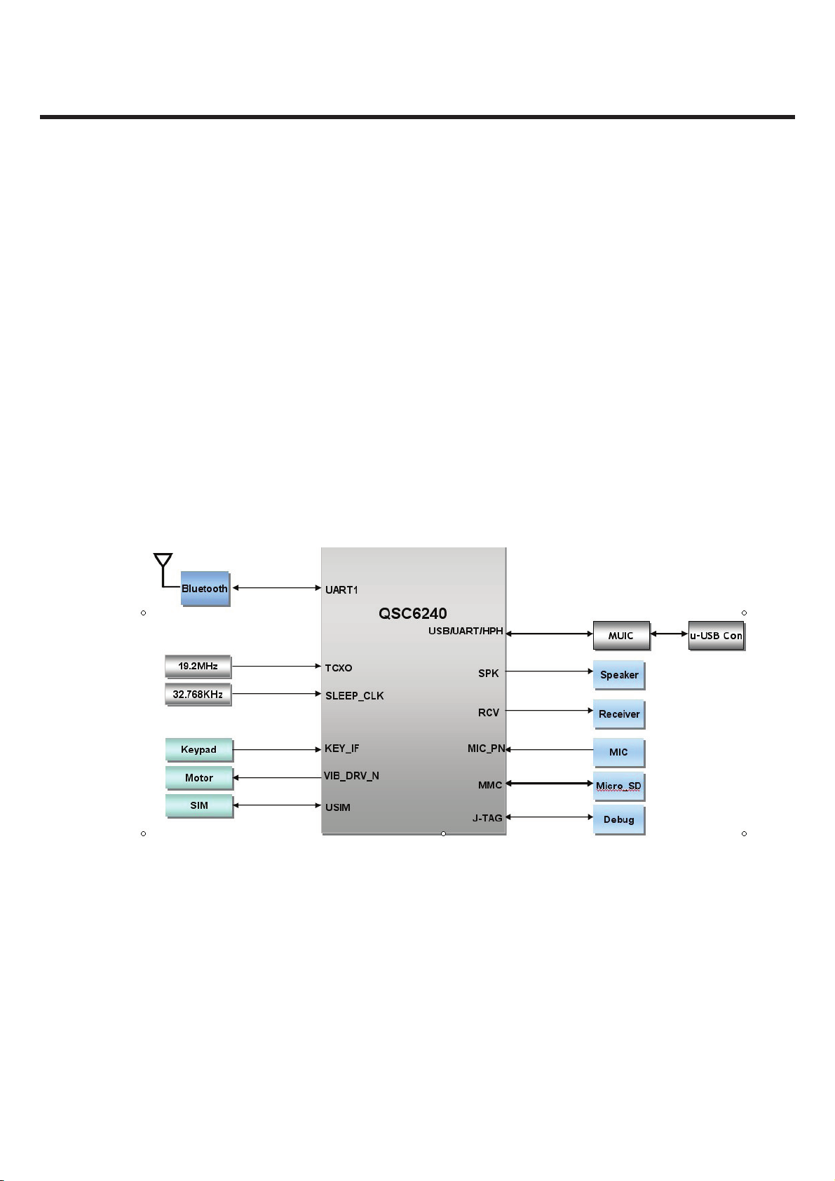
3.6.3 Connectivity
QSC6240 has connectivity features as below
– USB-OTG; USB LS, FS, and HS (2.0 compliant)
– I2C compatible for peripheral controls (1.8 V)
– UART: up to 4 Mbps
– Bluetooth 2.0 support via external SoC
– WLAN via external device (SDIO)
– NFC via external module (I2C)
– FM radio via external module (I2C)
– USIM, SIM, and USB-UICC support; 1.8 and 3 V
– Keypad interface
– SPI (master only) for peripheral support
– Two secure digital controllers — WLAN and secure digital (SD) cards
3. Technical Brief
Figure 2.1.3 The connectivity of GU280
Copyright © 2009 LG Electronics. Inc. All right reserved.
Only for training and service purposes
- 29 -
LGE Internal Use Only
3. Technical Brief
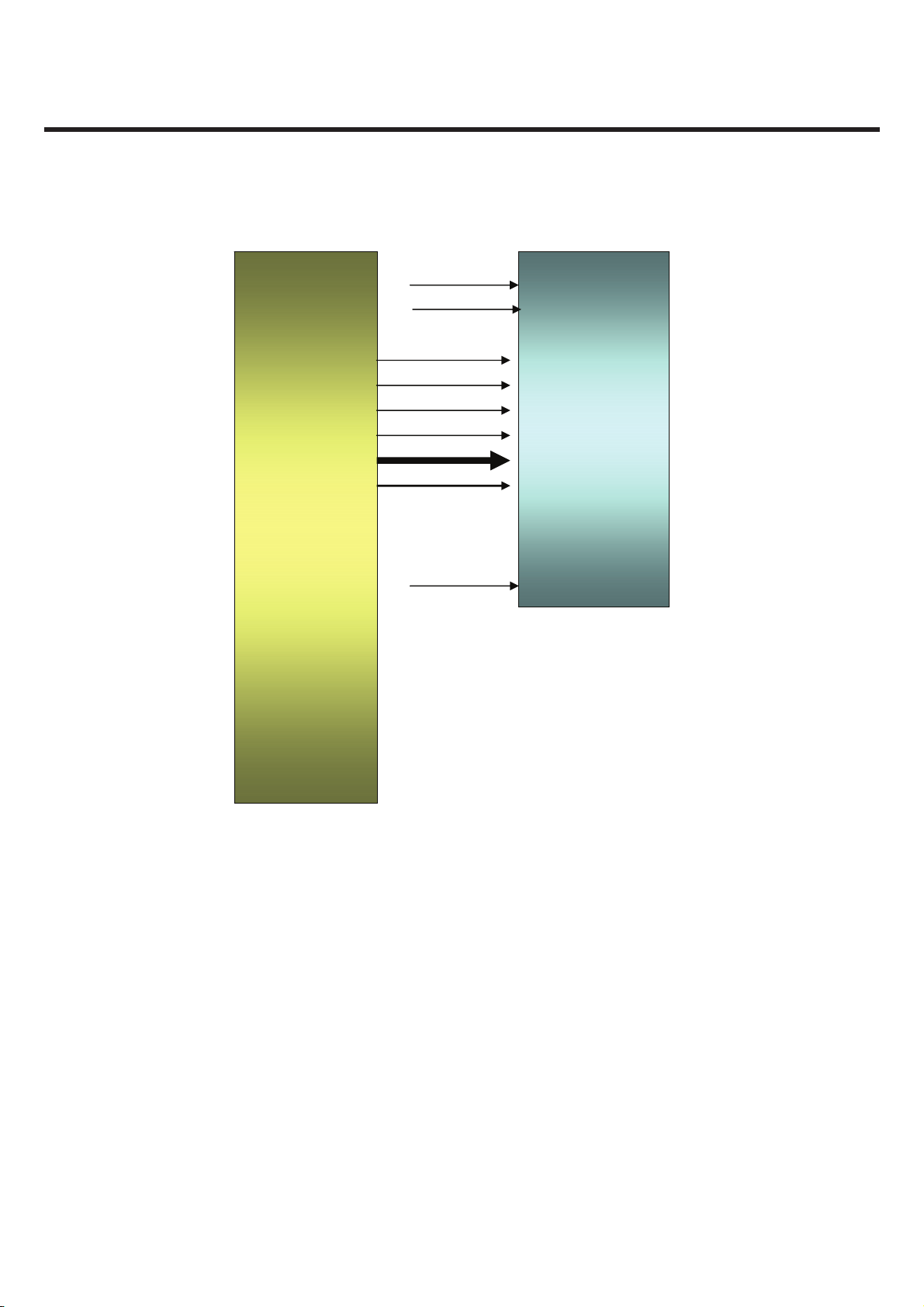
3.6.4 GPIOs
QSC6240 has 78 configurable I/O pins
UART_BT_SEL
I2C_SDA_BL
I2C_SCL_BL
113RK2.2
I2C2_SCL
I2C2_SDA
I2C_SCL
I2C_SDA
VREG_MSMP_2.6V
V8.1_EMSM_GERV
8
0
3R
K2.2903R
K2.2
BT_PWR_ON
LCD_MAKER_ID
CAM_LDO_EN
103R
203R
K7.4
K7.4
GSM_SW_MODE
SLIDE_DETECT
LCD_BACKLIGHT_CONT
TRK_LO_ADJ
V8.1_MAC_ODL
VGA_CAM_PWDN
VGA_CAM_RST
703RK2.2
NAND_READY
CAMIF_MCLK
CAMIF_DATA[7]
CAMIF_DATA[6]
CAMIF_DATA[5]
CAMIF_DATA[4]
CAMIF_DATA[3]
CAMIF_DATA[2]
CAMIF_DATA[1]
CAMIF_DATA[0]
CAMIF_VSYNC
CAMIF_HSYNC
CAMIF_PCLK
BT_PCM_CLK
BT_PCM_DOUT
BT_PCM_DIN
BT_PCM_SYNC
KEY_ROW[0]
KEY_ROW[1]
KEY_ROW[2]
KEY_ROW[3]
KEY_ROW[4]
UART1_RFR_N
UART1_CTS_N
MICROSD_CLK
MICROSD_DATA[3]
MICROSD_DATA[2]
MICROSD_DATA[1]
MICROSD_DATA[0]
MICROSD_CMD
MICROSD_DETECT
PA_R0
PA_R1
ANT_SEL[0]
ANT_SEL[1]
ANT_SEL[2]
ANT_SEL[3]
LCD_RST
USIM_DATA
USIM_CLK
USIM_RST
USW_INT
LCD_IF[2]
CAM_PWDN
LCD_IF[1]
CAM_RST
LCD_VSYNC
KEY_COL[0]
KEY_COL[1]
KEY_COL[2]
KEY_COL[3]
KEY_COL[4]
C309
DNI
TP302
AC3
GPIO_77
AB1
GPIO_76
AB2
GPIO_75
AA3
GPIO_74
AB8
AA7
T14
C17
C16
A16
B16
A17
B17
E15
B15
A14
F14
A13
AC5
AB6
AC4
H10
H12
B10
A10
A11
C14
B14
F13
B13
C13
F12
B12
C12
E13
B11
E12
E11
C11
E14
AA1
AA2
F11
F10
AB4
AA6
AB5
AA5
AA4
AB3
C15
V8
W9
W8
W7
W6
V7
E8
F8
F7
E7
A7
B7
C9
B9
G6
C8
E9
B8
A8
W1
V1
V2
W2
W3
Y1
Y2
Y3
GPIO_73
GPIO_72
GPIO_71
GPIO_70
GPIO_69
GPIO_68
GPIO_67
GPIO_66
GPIO_65
GPIO_64
GPIO_63
GPIO_62
GPIO_61
GPIO_60
GPIO_59
GPIO_58
GPIO_57
GPIO_56
GPIO_55
GPIO_54
GPIO_53
GPIO_52
GPIO_51
GPIO_50
GPIO_49
GPIO_48
GPIO_47
GPIO_46
GPIO_45
GPIO_44
GPIO_43
GPIO_42
GPIO_41
GPIO_40
GPIO_39
GPIO_38
GPIO_37
GPIO_36
GPIO_35
GPIO_34
GPIO_33
GPIO_32
GPIO_31
GPIO_30
GPIO_29
GPIO_28
GPIO_27
GPIO_26
GPIO_25
GPIO_24
GPIO_23
GPIO_22
GPIO_21
GPIO_20
GPIO_19
GPIO_18
GPIO_17
GPIO_16
GPIO_15
GPIO_14
GPIO_13
GPIO_12
GPIO_11
GPIO_10
GPIO_9
GPIO_8
GPIO_7
GPIO_6
GPIO_5
GPIO_4
GPIO_3
GPIO_2
GPIO_1
GPIO_0
TP
Figure 2.1.4 GPIOs of GU280
LGE Internal Use Only Copyright © 2009 LG Electronics. Inc. All right reserved.
- 30 -
Only for training and service purposes
3. Technical Brief
3.6.5 Air interfaces
The supported air-interface standards and features include: (See the RF technical description)
UMTS/WCDMA/GSM/GPRS/EDGE Specification Release ‘99 (3GPP R99)
GSM/GPRS/EDGE Specification Release 4 (3GPP R4)
UMTS/WCDMA Specification Release 5 (3GPP R5, QSC6270 only)
HSDPA and equalizer; 3.6 Mbps
Enhanced GPS position location using gpsOne (with RGR6240 IC, only QSC6270)
Integrated gpsOne functionality, featuring enhancements by SnapTrack®, Inc., to enable a
wide variety of location-based services and applications, including points of interest,
personal navigation, and friend finder
Simultaneous-GPS (processes GPS using dedicated circuitry while voice and/or data
signals continue to be processed separately)
1024x searcher, direct facility termination (DFT) accelerator, off-chip RAM for measured
data storage
3.6.6 Internal base band functions
Several baseband circuits within the QSC6240 device provide functions that are necessary only to
make the device operate properly — these functions are not generally used directly by other
handset circuits and functions.
PLLs and clock generation
Modes and resets
Security
Qfuse
JTAG/ETM
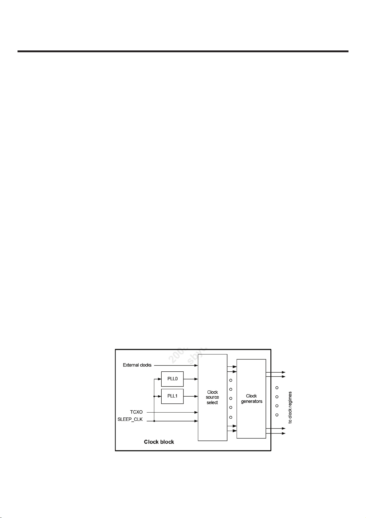
The clock block includes two PLLs, all phase-locked to the TCXO signal. These PLLs generate
several different stable, low-jitter clock signals that are distributed throughout the QSC device and
to external components as needed.
All the required WCDMA, GSM, GPS(only QSC6270), ARM, QDSP, and most peripheral clocks are derived in
some way from the TCXO (or XO) source for their operating modes, plus the 32.768 kHz
oscillator for their sleep modes
Figure 2.1.6 Clock block basic architecture of QSC6240
Copyright © 2009 LG Electronics. Inc. All right reserved.
Only for training and service purposes
- 31 -
LGE Internal Use Only
 Loading...