

LG GT400 Service Manual

Service Manual Model : GT400
Internal Use Only
Service Manual
GT400
Date: April, 2010 / Issue 1.0

Table Of Contents
1. INTRODUCTION ...................................... 5
1.1 Purpose .............................................................................. 5
1.2 Regulatory Information ............................................... 5
2. PERFORMANCE .......................................7
2.1 System Overview ............................................................7
2.2 Usable environment ...................................................... 8
2.3 Radio Performance ........................................................ 8
2.4 Current Consumption .................................................16
2.5 RSSI ....................................................................................16
2.6 Battery Bar ......................................................................16
2.7 Sound Pressure Level ..................................................17
2.8 Charging ..........................................................................18
3. Technical Brief .......................................19
3.1 Digital Baseband (DBB) & Multimedia Processor
....................................................................................................19
3.2 Visual part .......................................................................37
3.3 Audio Part .......................................................................43
3.4 GPADC (General Purpose ADC) and AUTOADC2 49
3.5 Charger control .............................................................50
3.6 Voltage Regulation ......................................................57
3.7 RF Technlcal Descrlption ............................................58
4. TROUBLE SHOOTING ............................69
4.1 Power ON Trouble ........................................................69
4.2 USB Trouble ....................................................................70
4.3 SIM Detect Trouble ......................................................71
4.4 MicroSD card Trouble .................................................72
4.5 Key and Touch Screen Trouble.................................73
4.6 Camera Trouble .............................................................77
4.7 Main LCD Trouble .........................................................79
4.8 Keypad Backlight Trouble .........................................82
4.9 Audio Trouble Shooting .............................................85
4.10 Charger Trouble Shooting ...................................100
4.11 Bluetooth Trouble ................................................... 103
4.12 RF Component ......................................................... 106
4.13 Procedure to check ................................................ 107
4.14 Checking Common Power Source Block ........ 108
4.15 Checking VCXO Block ............................................ 115
4.16 Checking Front End Module Block ................... 119
4.17 Checking Front End Module Block input logic
.................................................................................................120
4.18 Checking WCDMA Block ......................................131
4.19 Checking GSM Block .............................................. 144
5. DOWNLOAD ........................................156
5.1 LGDP2 ............................................................................ 156
5.2 Download..................................................................... 158
6. BLOCK DIAGRAM ................................159
7. CIRCUIT DIAGRAM ..............................161
8. BGA PIN MAP .......................................171
9. PCB LAYOUT ........................................177
10. CALIBRATION ....................................185
10.1 General Description ............................................... 185
10.2 Environment ............................................................. 185
10.3 Calibration Environment ...................................... 186
10.4 Program Operation ................................................ 187
11. EXPLODED VIEW & REPLACEMENT
PART LIST ...........................................193
11.1 EXPLODED VIEW ....................................................... 193
11.2 Replacement Parts ..................................................195
11.3 Accessory .................................................................... 221
Copyright © 2009 LG Electronics. Inc. All right reserved.
Only for training and service purposes
- 3 -
LGE Internal Use Only

LGE Internal Use Only Copyright © 2009 LG Electronics. Inc. All right reserved.
- 4 -
Only for training and service purposes

1. INTRODUCTION
1.1 Purpose
This manual provides the information necessary to repair, calibration, description and download the
features of this model.
1.2 Regulatory Information
A. Security
Toll fraud, the unauthorized use of telecommunications system by an unauthorized part (for example,
persons other than your company’s employees, agents, subcontractors, or person working on your
company’s behalf) can result in substantial additional charges for your telecommunications services. System
users are responsible for the security of own system. There are may be risks of toll fraud associated with your
telecommunications system. System users are responsible for programming and configuring the equipment
to prevent unauthorized use. The manufacturer does not warrant that this product is immune from the
above case but will prevent unauthorized use of common-carrier telecommunication service of facilities
accessed through or connected to it.
The manufacturer will not be responsible for any charges that result from such unauthorized use.
B. Incidence of Harm
If a telephone company determines that the equipment provided to customer is faulty and possibly causing
harm or interruption in service to the telephone network, it should disconnect telephone service until repair
can be done. A telephone company may temporarily disconnect service as long as repair is not done.
C. Changes in Service
A local telephone company may make changes in its communications facilities or procedure. If these
changes could reasonably be expected to affect the use of the this phone or compatibility with the network,
the telephone company is required to give advanced written notice to the user, allowing the user to take
appropriate steps to maintain telephone service.
D. Maintenance Limitations
Maintenance limitations on this model must be performed only by the manufacturer or its authorized agent.
The user may not make any changes and/or repairs expect as specifically noted in this manual. Therefore,
note that unauthorized alternations or repair may affect the regulatory status of the system and may void
any remaining warranty.
1. INTRODUCTION
1. INTRODUCTION
Copyright © 2009 LG Electronics. Inc. All right reserved.
Only for training and service purposes
- 5 -
LGE Internal Use Only

1. INTRODUCTION
E. Notice of Radiated Emissions
This model complies with rules regarding radiation and radio frequency emission as defined by local
regulatory agencies. In accordance with these agencies, you may be required to provide information such
as the following to the end user.
F. Pictures
The pictures in this manual are for illustrative purposes only; your actual hardware may look slightly
different.
G. Interference and Attenuation
Phone may interfere with sensitive laboratory equipment, medical equipment, etc.Interference from
unsuppressed engines or electric motors may cause problems.
H. Electrostatic Sensitive Devices
ATTENTION
Boards, which contain Electrostatic Sensitive Device (ESD), are indicated
by the sign. Following information is ESD handling:
• Service personnel should ground themselves by using a wrist strap when exchange system
boards.
• When repairs are made to a system board, they should spread the floor with anti-static mat
which is also grounded.
• Use a suitable, grounded soldering iron.
• Keep sensitive parts in these protective packages until these are used.
• When returning system boards or parts like EEPROM to the factory, use the protective
package as described.
2. INTRODUCTION
LGE Internal Use Only Copyright © 2009 LG Electronics. Inc. All right reserved.
- 6 -
Only for training and service purposes
2. PERFORMANCE
2. PERFORMANCE
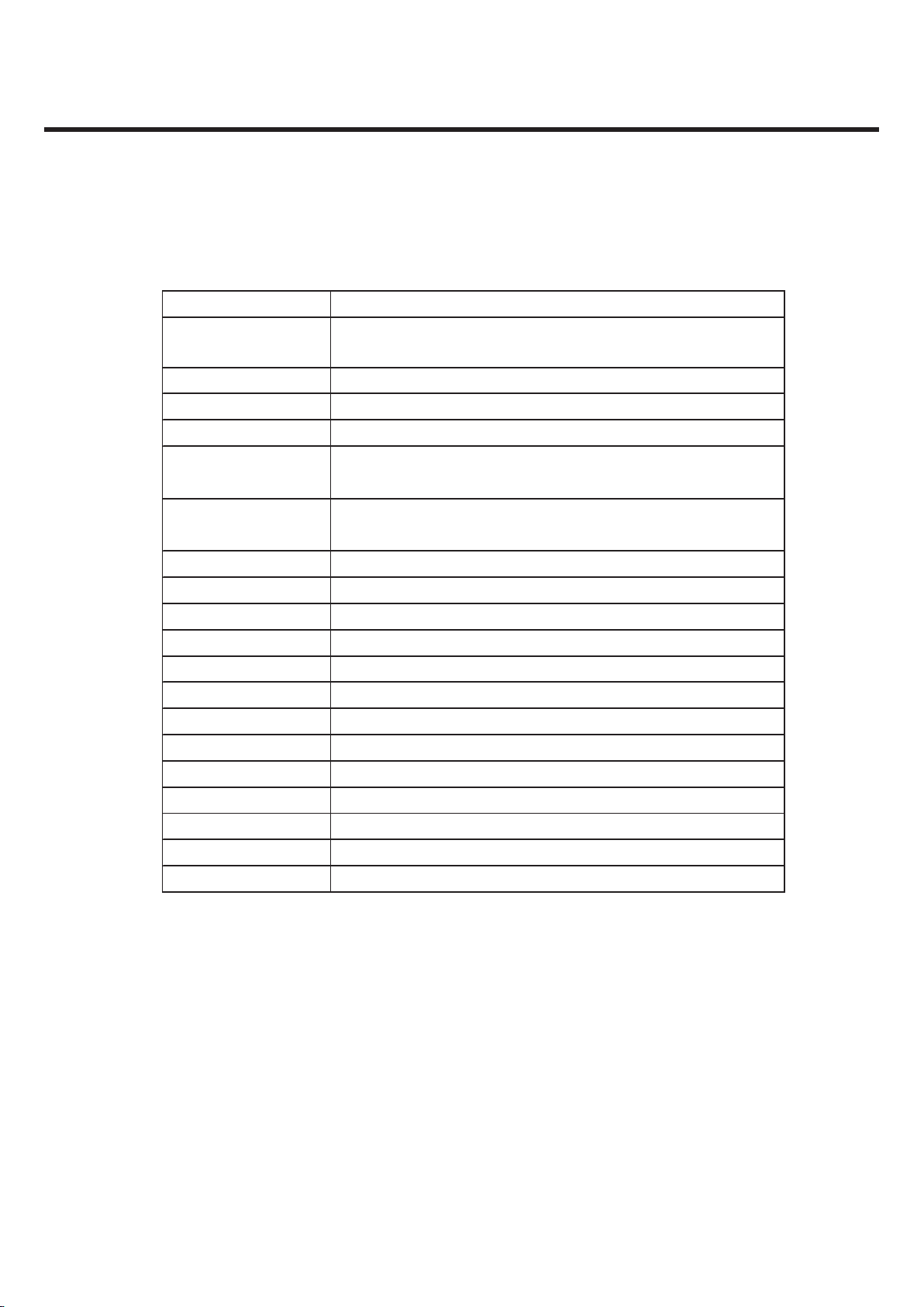
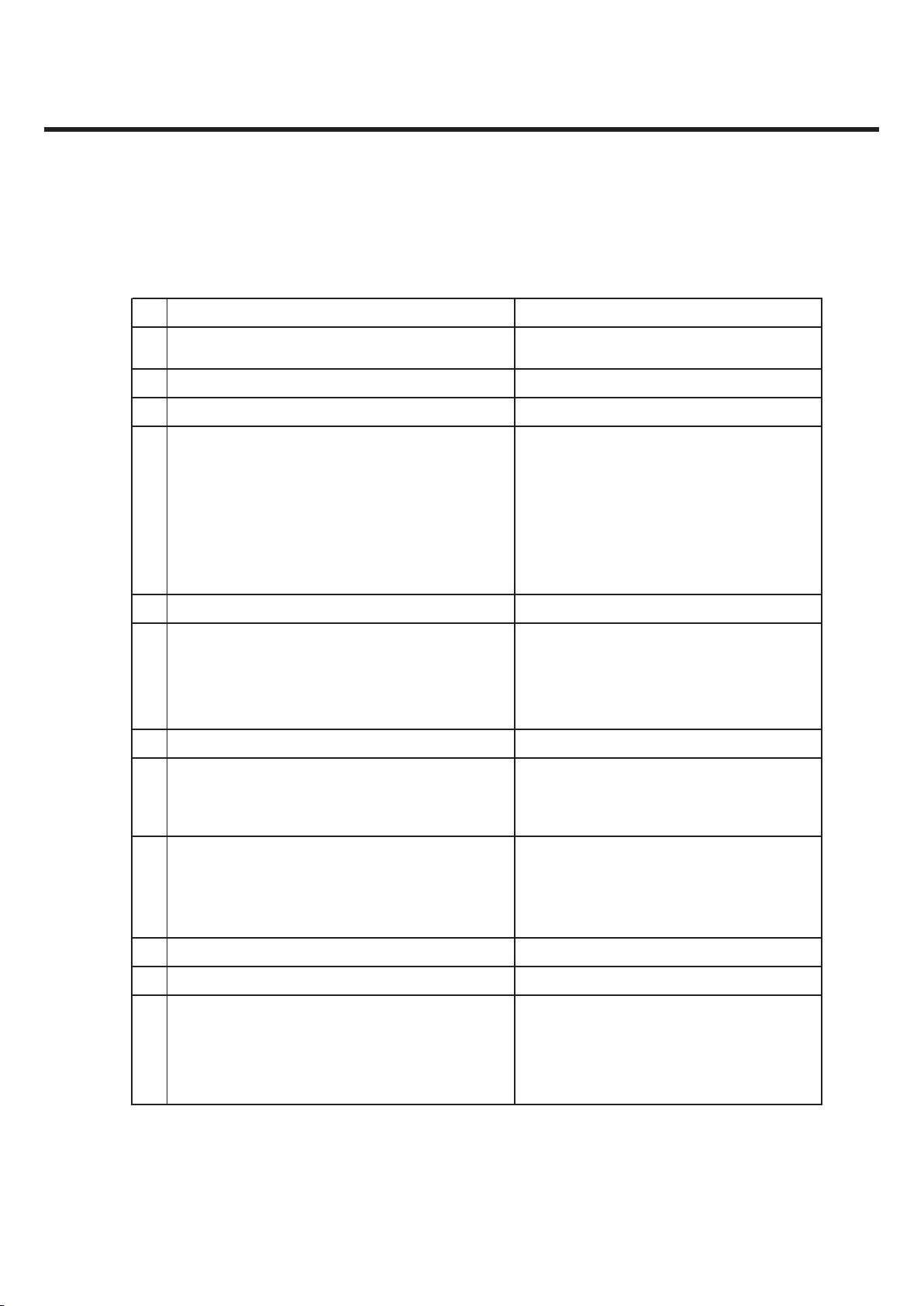
2.1 System Overview
Item Specification
Shape
GSM850/900/1800/1900 & WCDMA Band 1, 8
Bar type - Dual Mode Handset
Size 107 x 54.5 x 11.8 mm
Weight 98g (with standard battery)
Power 1000mAh Li-ion
Over 200 Min (WCDMA, Tx=10 dBm, Voice)
Over 200 Min (GSM, Tx=Max, Voice)
Over 300 hrs (WCDMA, DRX=7)
Over 300 hrs (GSM, Paging period=5)
Antenna Intenna type
Main LCD 3"(400x240), 262K TFT Color LCD
Main LCD BL White LED Backlight
Vibrator Yes (Coin Type)
Speaker Yes
MIC Yes (SMD Type)
Receiver Yes
Earphone Jack Yes
SIM Socket Yes(SIM Block Type) : 3.0V & 1.8V
Volume Key Push Type ( + , - )
Camera Key Push Type
External Memory Micro SD Socket
I/O Connect 5 Pins
Talk Time
Standby Time
2. PERFORMANCE
2. PERFORMANCE
Copyright © 2009 LG Electronics. Inc. All right reserved.
Only for training and service purposes
- 7 -
LGE Internal Use Only
2. PERFORMANCE
2.2 Usable environment
1) Environment
2) Environment (Accessory)
* CLA : 12~24V (DC)
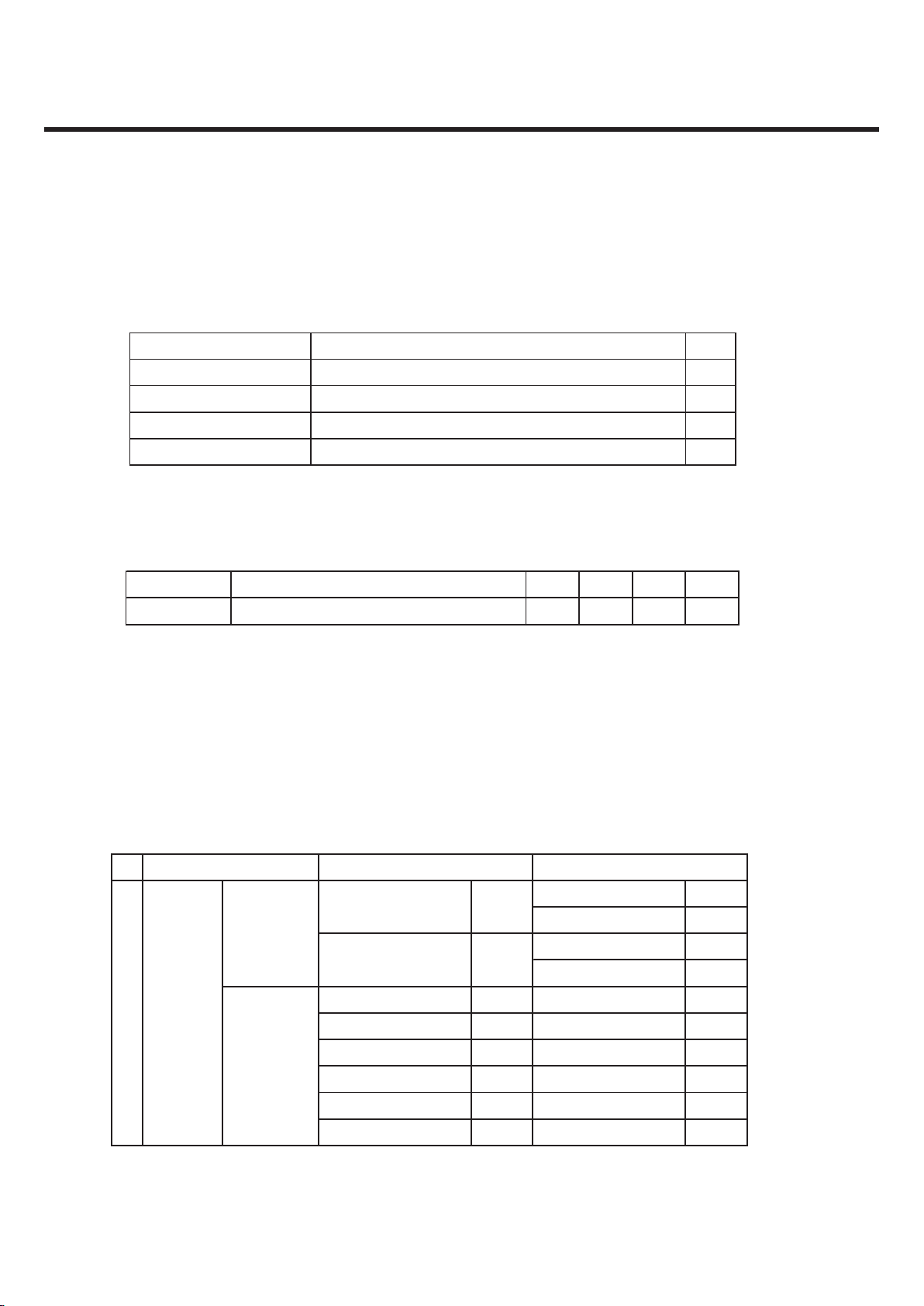
2.3 Radio Performance
1) Transmitter – GSM Mode
Item Spec. Unit
Voltage 3.7 (Typ), 3.4 (Min), (Shut Down: 3.2) V
Operating Temp. -20 ~ + 60 °C
Storage Temp. -30 ~ + 85 °C
Humidity max. 85 %
Item Spec. Min Typ. Max Unit
Power Available power 100 220 240 Vac
No
9k ~ 1GHz -39dBm
1G ~ 1710MHz -33dBm
1710M ~ 1785MHz -39dBm
1785M ~ 12.75GHz -33dBm
100k ~ 880MHz -60dBm 100k ~ 880MHz -60dBm
880M ~ 915MHz -62dBm 880M ~ 915MHz -62dBm
915M ~ 1000Mz -60dBm 915M ~ 1000MHz -60dBm
1G ~ 1.71GHz -50dBm 1G ~ 1.71GHz -50dBm
1.71G ~ 1.785GHz -56dBm 1.71G ~ 1.785GHz -56dBm
1.785G ~ 12.75GHz -50dBm 1.785G ~ 12.75GHz -50dBm
Item
1
DCS/PCSGSM
Conducted
Spurious
Emission
-39dBm
-33dBm
MS allocated
Channel
100k ~ 1GHz
Idle Mode
1G ~ 12.75GHz
2. PERFORMANCE
LGE Internal Use Only Copyright © 2009 LG Electronics. Inc. All right reserved.
- 8 -
Only for training and service purposes
2. PERFORMANCE
No
30M ~ 1GHz -36dBm
MS allocated 1G ~ 1710MHz -30dBm
Channel 1710M ~ 1785MHz -36dBm
Radiated 1785M ~ 4GHz -30dBm
Spurious 30M ~ 880MHz -57dBm 30M ~ 880MHz -57dBm
Emission 880M ~ 915MHz -59dBm 880M ~ 915MHz -59dBm
Idle Mode 915M ~ 1000Mz -57dBm 915M ~ 1000MHz -57dBm
1G ~ 1.71GHz -47dBm 1G ~ 1.71GHz -47dBm
1.71G ~ 1.785GHz -53dBm 1.71G ~ 1.785GHz -53dBm
1.785G ~ 4GHz -47dBm 1.785G ~ 4GHz -47dBm
2
0 ~ 100kHz +0.5dB 0 ~ 100kHz +0.5dB
200kHz -30dB 200kHz -30dB
250kHz -33dB 250kHz -31dB
Due to 400kHz -60dB 400kHz -33dB
Output RF modulation 600 ~ 1800kHz -66dB 600 ~ 1800kHz -60dB
Spectrum 1800 ~ 3000kHz -69dB 1800 ~ 6000kHz -60dB
3000 ~ 6000kHz -71dB ˻6000kHz -73dB
˻
6000kHz -77dB
400kHz -19dB 400kHz -22dB
600kHz -21dB 600kHz -24dB
1200kHz -21dB 1200kHz -24dB
1800kHz -24dB 1800kHz -27dB
1
DCS/PCSGSM
-36dBm
-30dBm
30M ~ 1GHz
1G ~ 4GHz
Item
Frequency Error ±0.1ppm ±0.1ppm
3 Phase Error
±5(RMS) ±5(RMS)
±20(PEAK) ±20(PEAK)
Condition TU50: ±100Hz TU50: ±150Hz
3dB below reference sensitivity 3dB below reference sensitivity
Frequency Error Under RA250: ±200Hz RA250: ±250Hz
TU3: ±150Hz TU1.5: ±200Hz
5
Due to
Switching
transient
4
Multipath and Interference HT100: ±100Hz HT100: ±250Hz
2. PERFORMANCE
Copyright © 2009 LG Electronics. Inc. All right reserved.
Only for training and service purposes
- 9 -
LGE Internal Use Only
2. PERFORMANCE
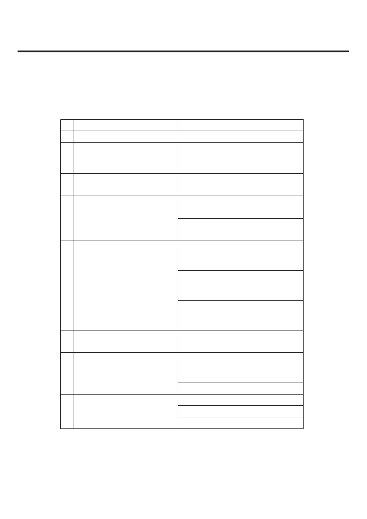
No Item
800kHz
Power
control
Level
Power
(dBm)
Tolerance
(dB)
Power
control
Level
Power
(dBm)
Tolerance
(dB)
5 33 ±3 0 30 ±3
6 31 ±3 1 28 ±3
7 29 ±3 2 26 ±3
8 27 ±3 3 24 ±3
9 25 ±3 4 22 ±3
10 23 ±3 5 20 ±3
11 21 ±3 6 18 ±3
12 19 ±3 7 16 ±3
13 17 ±3 8 14 ±3
14 15 ±3 9 12 ±4
15 13 ±3 10 10 ±4
16 11 ±5 11 8 ±4
17 9 ±5 12 6 ±4
18 7 ±5 13 4 ±4
19 5 ±5 14 2 ±5
15 0 ±5
9 Burst timing
GSM DCS/PCS
Frequency offset
Intermodulation product should
be Less than 55dB below the
level of Wanted signal
Mask IN
Intermodulation
attenuation
–7
8
Transmitter
Output Power
Mask IN
2. PERFORMANCE
LGE Internal Use Only Copyright © 2009 LG Electronics. Inc. All right reserved.
- 10 -
Only for training and service purposes
2) Transmitter – WCDMA Mode
2. PERFORMANCE
No Item Specification
1 Maximum Output Power
Class3: +24dBm(+1/-3dB)
Class4: +21dBm(±2dB)
2 Frequency Error ±0.1ppm
3 Open Loop Power control in uplink ±9dB@normal, ±12dB@extreme
4 Inner Loop Power control in uplink
Adjust output (TPC command)
cmd 1dB 2dB 3dB
+1 +0.5/1.5 +1/3 +1.5/4.5
0 -0.5/+0.5 -0.5/+0.5 -0.5/+0.5
-1 -0.5/-1.5 -1/-3 -1.5/-4.5
group(10equal command group)
+1 +8/+12 +
5 Minimum Output Power -50dBm(3.84MHz)
6 Out-of-synchronization handling of output power
Qin/Qout:DPCCH quality levels
Toff@DPCCH/lor:-22->-28dB
Ton@DPCCH/lor:-24->-18dB
7 Transmit OFF Power -56dBm(3.84M)
8 Transmit ON/OFF Time Mask
±25us
PRACH, CPCH, uplink compressed mode
9 Change of TFC
±25us
power varies according to the data rate
DTX: DPCH off
(minimize interference between UE)
10 Power setting in uplink compressed ±3dB(after 14slots transmission gap)
11 Occupied Bandwidth(OBW) 5MHz(99%)
12 Spectrum emission Mask
-35-15*(˭f-2.5)dBc@˭f=2.5~3.5MHz, 30k
-35-1*(˭f-3.5)dBc@˭f=3.5~7.5MHz, 1M
-39-10*(˭f-7.5)dBc@˭f=7.5~8.5MHz, 1M
-49 dBc@˭f=8.5~12.5MHz, 1M
2. PERFORMANCE
Copyright © 2009 LG Electronics. Inc. All right reserved.
Only for training and service purposes
- 11 -
LGE Internal Use Only
2. PERFORMANCE
2. PERFORMANCE
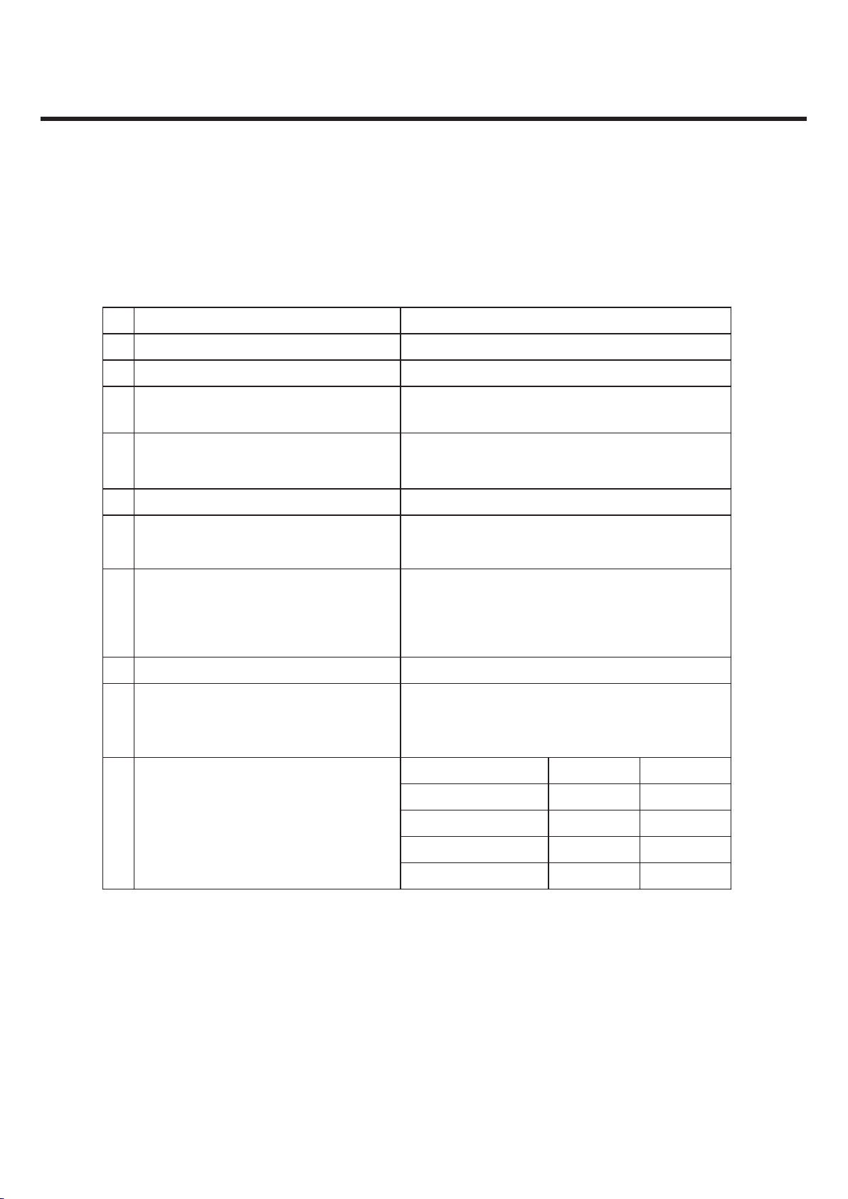
No Item Specification
13 Adjacent Channel Leakage Ratio(ACLR)
33dB@5MHz, ACP>-50dBm
43dB@10MHz, ACP>-50dBm
14
Spurious Emissions
*: additional requirement
-36dBm@f=9~150KHz, 1k BW
-36dBm@f=150KHz~30MHz, 10k
-36dBm@f=30~1000MHz, 100k
-30dBm@f=1~12.75GHz, 1M
-41dBm*@1893.5~1919.6MHz, 300k
-67dBm*@925~935MHz, 100k
-79dBm*@935~960MHz, 100k
-71dBm*@1805~1880MHz, 100k
15 Transmit Intermodulation
-31dBc@5MHz, Interferer -40dBc
-41dBc@10MHz, Interferer -40dBc
16 Error Vector Magnitude(EVM)
17.5% (>-20dBm)
(@12.2k, 1DPDCH+1DPCCH)
17 Transmit OFF Power
-15dB@SF=4, 768kbps,
multi-code transmission
3) Receiver - GSM Mode
No GSM DCS/PCS
1 -105dBm -105dBm
2 C/Ic=7dB C/Ic=7dB
3 Adjacent Channel 200kHz C/Ia1=-12dB C/Ia1=-12dB
Rejection 400kHz C/Ia2=-44dB C/Ia2=-44dB
4
Wanted Signal: -98dBm
1’st interferer: -44dBm
2’st interferer: -45dBm
Wanted Signal: -96dBm
1’st interferer: -44dBm
2’st interferer: -44dBm
5
Wanted Signal: -101dBm
Unwanted Signal: Depend on freq.
Wanted Signal: -101dBm
Unwanted Signal: Depend on freq.
Blocking Response
(TCH/FS Class II, RBER)
Item
Sensitivity (TCH/FS Class II)
Co-Channel Rejection
(TCH/FS Class II, RBER,
TUhigh/FH)
Intermodulation Rejection
LGE Internal Use Only Copyright © 2009 LG Electronics. Inc. All right reserved.
- 12 -
Only for training and service purposes
2. PERFORMANCE
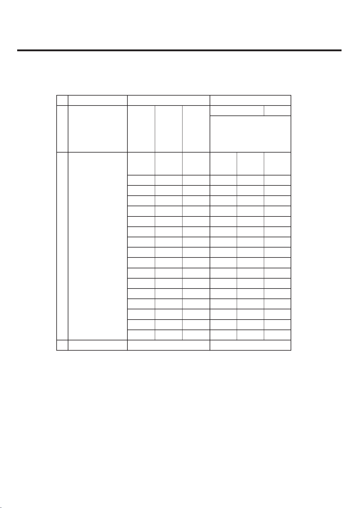
4) Receiver – WCDMA Mode
No Item Specification
1 Reference Sensivitivity Level -106.7dBm(3.84M)
2 Maximum Input Level
-25dBm(3.84MHz)
-44dBm/3.84MHz(DPCH_Ec)
UE@+20dBm output power(class3)
3 Adjacent Channel Selectivity(ACS)
33dB
UE@+20dBm output power(class3)
-56dBm/3.84MHz@10MHz
UE@+20dBm output power(class3)
-44dBm/3.84MHz@15MHz
UE@+20dBm output power(class3)
-44dBm/3.84MHz@f=2050~2095 &
2185~2230MHz, band a)
UE@+20dBm output power(class3)
-30dBm/3.84MHz@f=2025~2050 &
2230~2255MHz, band a)
UE@+20dBm output power(class3)
-15dBm/3.84MHz@f=1~2025 &
2255~12500MHz, band a)
UE@+20dBm output power(class3)
6 Spurious Response
-44dBm CW
UE@+20dBm output power(class3)
-46dBm CW@10MHz &
-46dBm/3.84MHz@20MHz
UE@+20dBm output power(class3)
-57dBm@f=9KHz~1GHz, 100k BW
-47dBm@f=1~12.75GHz, 1M
-60dBm@f=1920~1980MHz, 3.84MHz
-60dBm@f=2110~2170MHz, 3.84MHz
8 Spurious Emissions
4 In-band Blocking
5 Out-band Blocking
7 Intermodulation Characteristic
2. PERFORMANCE
Copyright © 2009 LG Electronics. Inc. All right reserved.
Only for training and service purposes
- 13 -
LGE Internal Use Only
2. PERFORMANCE
2. PERFORMANCE
5) Bluetooth Mode
5.1) Transmitter
No Item
1 Out Power
2 Power Density
3 Power Control
4 TX Output Spectrum -Frequency range
5 TX Output Spectrum -20dB Bandwidth
6 Tx Output Spectrum -Adjacent channel Po
7 Modulation Characteristics
8 Init. Carrier Freq. Tolerance
9 Carrier Frequency Drift
Freq.Range Operating Standby
30MHz~1GHz -36dBm -57dBm
Above 1GHz~12.75GHz -30dBm -47dBm
1.8~1.9GHz -47dBm -47dBm
5.15~5.3GHz -47dBm -47dBm
Power density < 20dBm per 100kHz EIRP
Option
2dB ˺ step size ˺ 8dB
fmax & fmin @ below the level of -30dBm
(100khz BW) within 2.4GHz~2.4835GHz
10
1 slot : ˺ ± 25kHz
3 slot : ˺ ± 40kHz
5 slot : ˺ ± 40kHz
Maximum drift rate ˺ 20KHz/50usec
Specification
Out of Band Spurious Emissions
˺
1MHz
˺ -20dBm @ C/I = 2MHz
˺
-40dBm @ C/I ˻ 3MHz
140kHz ˺ delta f1 avg ˺175kHz
delta f2max ˻115kHz at least 99.9% of all
deltaf2max
delta f2avg/deata f1avg˻0.8
˺
±75KHz
Class 2 : -6~4dBm
LGE Internal Use Only Copyright © 2009 LG Electronics. Inc. All right reserved.
- 14 -
Only for training and service purposes
2. PERFORMANCE
2. PERFORMANCE
5.2) Receiver
No Item
1 Sensitivity single slot packets
2 Sensitivity multi slot packets
Interference Ratio
Co-Channel interference, C/I co-channel 11dB
Adjacent(1MHz)interference, C/I 1MHz 0dB
Adjacent(2MHz)interference, C/I 2MHz -30dB
Adjacent(˻3MHz)interference, C/I ˻3MHz -40dB
Adjacent(˻3MHz)interference to in band -9dB
mirror frequency, C/I image ±1MHz -20dB
interfering Signal Frequency Power Level
30MHz~2000MHz -10dBm
2000MHz~2400MHz -27dBm
2500MHz~3000MHz -27dBm
3000MHz~12.75GHz -10dBm
5 Intermodluation Performance
6 Maximum Input Level
BER ˺ 0.1%@wanted signal -67dBm
BER ˺ 0.1%@wanted signal -64dBm
static sinwave signal at f1=-39dBm
a BT modulated signal f2=-39dBm(payload PRBS15)
BER ˺ 0.1%@-20dBm
Specification
BER0.1%@-70dBm
BER˺0.1%@-70dBm
BER ˺ 0.1%@ (Low,Mid,High Frequency)
2405MHz, 2441MHz, 2477MHz
C/I performance
Blocking Characteristic
3
4
Copyright © 2009 LG Electronics. Inc. All right reserved.
Only for training and service purposes
- 15 -
LGE Internal Use Only
2. PERFORMANCE
2. PERFORMANCE
GSM WCDMA
BAR 7 -92ᇹ2 =< RSSI -90ᇹ2 =< RSSI
BAR 5 -97ᇹ2 =< RSSI -105ᇹ2 =< RSSI
BAR 4 -100ᇹ2 =< RSSI -109ᇹ2 =< RSSI
BAR 2 -103ᇹ2 =< RSSI -111ᇹ2 =< RSSI
BAR 1 -105ᇹ2 =< RSSI -113ᇹ2 =< RSSI
BAR 0 -105ᇹ2 > RSSI -113ᇹ2 > RSSI
2.4 Current Consumption
(VT test : Speaker off, LCD backlight On)
Stand by Voice Call VT
310 Hours = 3.2mA 210 Min = 280 mA 150 Min = 400 mA
(DRX=7) (Tx=10dBm) (Tx=10dBm)
300 Hours = 3.3 mA 205 Min = 290 mA
(paging=5period) (Tx=Max)
WCDMA
GSM
2.5 RSSI
2.6 Battery Bar
Indication Voltage
BAR 3 (100%) : level full 4.17V · 0.05V
BAR 3 (40%) -> 2 ᵐ (12%) 3.72 · 0.05V
BAR 2 (12%) -> 1 ᵐ (3%) 3.62 · 0.05V
BAR 1 (3%) -> Icon Blinking &
Alerting Sound
3.53 · 0.05V
POWER OFF 3.20 · 0.05V
LGE Internal Use Only Copyright © 2009 LG Electronics. Inc. All right reserved.
- 16 -
Only for training and service purposes
2. PERFORMANCE
2.7 Sound Pressure Level
No
NOM
MAX
NOM -1±3dB
MAX -15±3dB
NOM
MAX
NOM
MAX
5
6
NOM
MAX
NOM -47dBPA under
MAX -36dBPA under
A NOM
C MAX
O NOM -1±3dB
U MAX -12±3dB
S NOM
T MAX
I NOM
C MAX
13
14
NOM
MAX
NOM -45dBPA under
MAX -40dBPA under
SEND
REV.
SEND
REV.
SEND
REV.
SEND
REV.
Specification
1 Sending Loudness Rating (SLR) 8±3dB
Test Item
3 Side Tone Masking Rating (STMR)
2 Receiving Loudness Rating (RLR)
4 Echo Loss (EL) 40dB over
refer to TABLE 30.3
Receiving Distortion (RD) refer to TABLE 30.4
17dB over
8±3dB
-64dBm0p under
8 Idle Noise-Receiving (INR)
MS
7 Idle Noise-Sending (INS)
Sending Distortion (SD)
40dB over
Sending Distortion (SD) refer to TABLE 30.3
25dB over
refer to TABLE 30.4
15 Idle Noise-Sending (INS) -55dBm0p under
16 Idle Noise-Receiving (INR)
HEAD
SET
Receiving Distortion (RD)
17
TDMA NOISE
GSM: Power Level: 5
DCS: Power Level: 0
(Cell Power: -90 ~ -105dBm)
Acoustic(Max Vol.)
MS/HEADSET SLR: 8±3dB
MS/HEADSET RLR: -13±1dB/-
15dB
(SLR/RLR: mid-Value Setting)
MS
GSM
-62dBm under
DCS
Headset
GSM
DCS
9 Sending Loudness Rating (SLR)
10 Receiving Loudness Rating (RLR)
11 Side Tone Masking Rating (STMR)
12 Echo Loss (EL)
2. PERFORMANCE
Copyright © 2009 LG Electronics. Inc. All right reserved.
Only for training and service purposes
- 17 -
LGE Internal Use Only

2. PERFORMANCE
2. PERFORMANCE
2.8 Charging
· Normal mode: Complete Voltage: 4.2V
Charging Current: 700mA
· Await mode: In case of During a Call, should be kept 3.9V
(GSM: It should be kept 3.9V in all power level
WCDMA: It will not be kept 3.9V in some power level)
· Extend await mode: At Charging prohibited temperature(0¶C under or 45¶C over)
(GSM: It should be kept 3.7V in all power level
WCDMA: It will not be kept 3.7V in some power level)
LGE Internal Use Only Copyright © 2009 LG Electronics. Inc. All right reserved.
- 18 -
Only for training and service purposes

3. TECHNICAL BRIEF
3.1 Digital Baseband (DBB) & Multimedia Processor
3.1.1 General Description
y Access subsystem
- Access Central Processing Unit (CPU) subsystem – ARM926, Joint Test Action Group (JTAG), Embedded
Trace Module (ETM), Instruction and Data (I&D)-cache, and I&D-TCM
- Access peripheral subsystems – Subscriber Identity Module (SIM) interface, IrDA®, Universal Serial Bus
(USB), Universal Asynchronous Receiver/Transmitter (UART), and so on
- Digital Signal Processor (DSP) subsystem – CEVA-X1620, JTAG, Static Random Access Memory (SRAM),
and Program Data Read Only Memory (PDROM)
- EDGE/GSM/GPRS (EGG) subsystem – EGG hardware accelerators
- WCDMA subsystem – WCDMA hardware accelerators
Application subsystem
- Application CPU subsystem – containing ARM926, JTAG, ETM, I&D-cache, and I&D-TCM
- Application peripheral subsystems – I2C™, keypad, UART, and so on
- Graphics subsystem – XGAM subsystem
- Audio Processing Execution (APEX) and video encoder subsystems
In addition to the two subsystems above, there is also a test block, chip control block, and a pad
multiplexing block residing at the top level
y DSP
- The Digital Signal Processor Subsystem (DSPSUB) includes a DSP megacell, which contains the DSP CPU
together with a tightly coupled memory. The DSP is the Ceva-X 1620 core with a 64 KiB instruction
RAM and a 64 KiB data RAM. It also contains debug logic and interfaces. In addition to the megacell,
the DSPSUB includes external memories, peripheral units, and interfaces. The DSP megacell is clocked
at 208 MHz.
- The DSPSUB includes an AHB master and an AHB slave interface. The AHB master provides a direct access
to the Internal Random Access Memory (IRAM) in the EGG core through the AHB. The AHB slave
interface allows the CPU and the DMA to access in the program and data RAM residing in the DSPSUB.
y Image Signal Processor(MV9319)
- MV9319 is high-end Image Signal Processor (ISP) supporting image sensors up to 5 mega pixels. Its
powerful image processing fuctions such as edge enhancement, color correction, advance
interpolation, Auto White Balancing increases the quality of sensor image. MV9319 also supports
serial interfaces to Flash LED control.
y WCDMA subsystem
- The digital baseband controller WCDMA subsystem incorporate a WCDMA modem
- An interface to the WCMDA together with memory control and an internal single port RAM. The WCDMA
subsystem has three AHB slave interfaces.
- The Ericsson DB 3200 also includes HSDPA class 6 functionality.
- The WCDMA subsystem is handled and provided by Ericsson.
y XGAM subsystem
- The XGAM subsystem is a graphics acceleration module that provides hardware support in the creation of
visual imagery and the transfer of this data to a display. The XGAM also provides support for
connecting a Camera module. The visual data could be graphics, still images, or video.
- The XGAM subsystem is handled and provided by Ericsson.
y Operation and Services
- IC™ Interface
- SIM Interfaces
- General Purpose I/O (GPIO) Interface
- External Memory Interface that supports NAND, NOR, PSRAM, SDRAM,
- JTAG
- RTC
- ETM9
3. Technical Brief
3. TECHNICAL BRIEF
Copyright © 2009 LG Electronics. Inc. All right reserved.
Only for training and service purposes
- 19 -
LGE Internal Use Only
3. TECHNICAL BRIEF
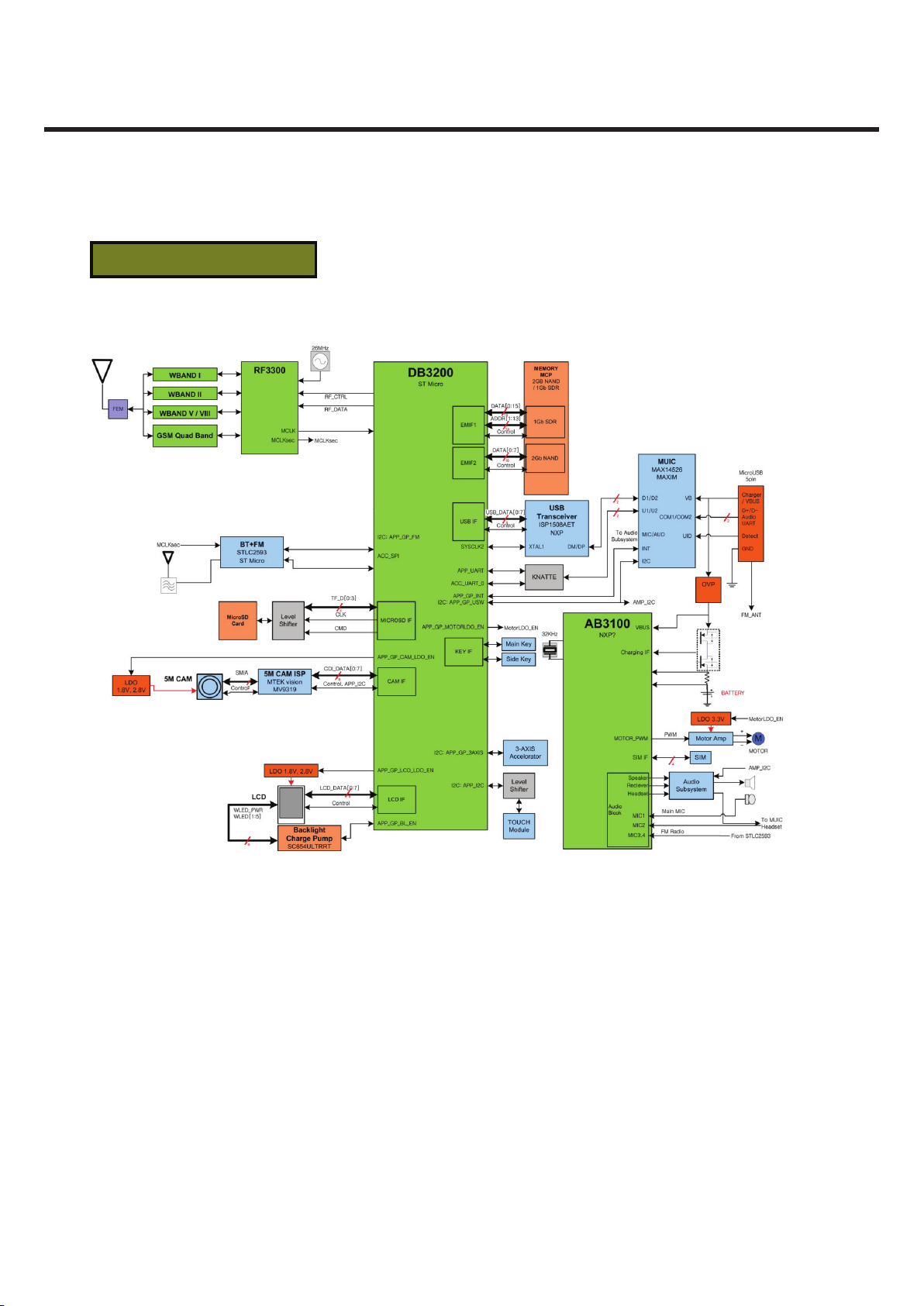
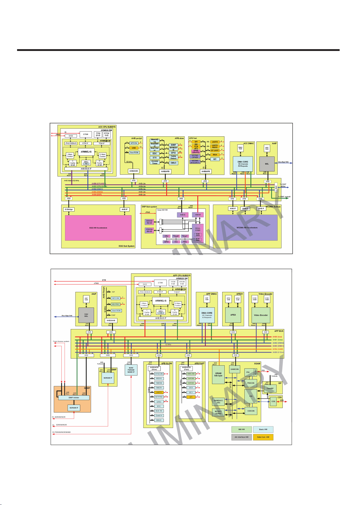
Figure 3-1-1 GT405 Block Diagram
3. Technical Brief
GT400 Block Diagram
LGE Internal Use Only Copyright © 2009 LG Electronics. Inc. All right reserved.
- 20 -
Only for training and service purposes
3.1.2 External memory interface
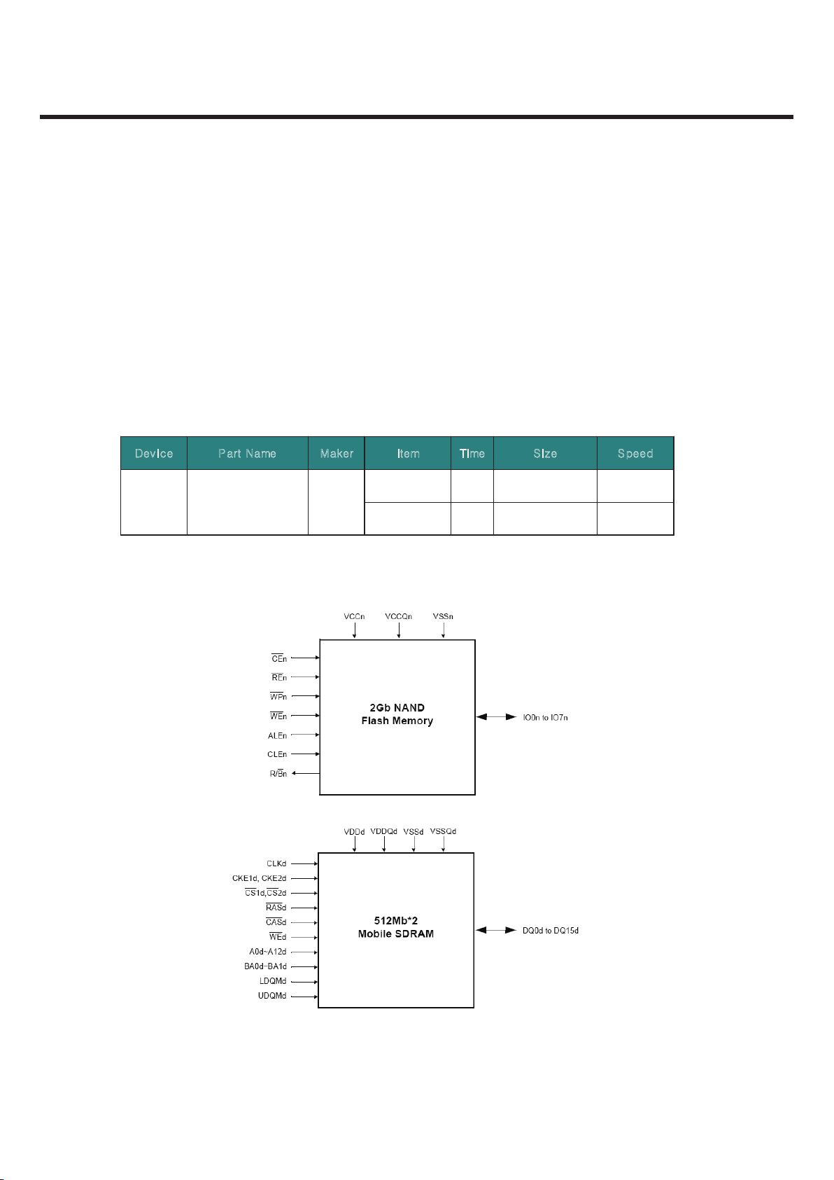
RF calibration data, Audio parameters and battery calibration data etc are stored in flash memory
area.
A. GT500
y 2Gb NAND flash memory + 1Gb SDRAM
Table 3- 1- 1. External Memory Interface Spec. of GT500
Figure 3- 1- 2. External Memory Configuration of GT500
͵ΖΧ ΚΔΖ ΒΣΥͿΒΞΖ ;ΒΜΖΣ ͺΥΖΞ ΅ΚΞΖ ΄ΚΫΖ ΄ΡΖΖΕ
ΣΠΘΣΒΞΤΡΖΖΕ υΤ ΡΒΘΖͳΪΥΖ ;ͳΪΥΖΤ
ͶΣΒΤΖΤΡΖΖΕ ΞΤ ͳΝΠΔΜͼͳΪΥΖ ;ͳΪΥΖΤ
ͿͲͿ͵ΗΝΒΤΙ ͼ͵Ͳʹ͵͵ ΄ΒΞΤΦΟΘ
y Data Communication
- IrDA ® (SIR)
- UARTs (ACB, EDB (RS232))
- USB
y Package
- 12 by 12 mm 376 balls, 0.5mm pitch TFBGA Production Package
3. Technical Brief
3.1.2 External memory interface
RF calibration data, Audio parameters and battery calibration data etc are stored in flash memory area.
A. GT400
y 2Gb NAND flash memory + 1Gb SDRAM
Table 3- 1- 1. External Memory Interface Spec. of GT400
Figure 3- 1- 2. External Memory Configuration of GT400
͵ΖΧ ΚΔΖ ΒΣΥͿΒΞΖ ;ΒΜΖΣ ͺΥΖΞ ΅ΚΞΖ ΄ΚΫΖ ΄ΡΖΖΕ
ΣΠΘΣΒΞΤΡΖΖΕ υΤ ΡΒΘΖͳΪΥΖ ;ͳΪΥΖΤ
ͶΣΒΤΖΤΡΖΖΕ ΞΤ ͳΝΠΔΜͼͳΪΥΖ ;ͳΪΥΖΤ
ͿͲͿ͵ΗΝΒΤΙ ͼ͵Ͳʹ͵͵ ΄ΒΞΤΦΟΘ
y Data Communication
- IrDA ® (SIR)
- UARTs (ACB, EDB (RS232))
- USB
y Package
- 12 by 12 mm 376 balls, 0.5mm pitch TFBGA Production Package
3. Technical Brief
3. TECHNICAL BRIEF
Copyright © 2009 LG Electronics. Inc. All right reserved.
Only for training and service purposes
- 21 -
LGE Internal Use Only
3. TECHNICAL BRIEF
3.1.3 Hardware Architecture
A. Block Diagram
3. Technical Brief
3.1.3 Hardware Architecture
A. Block Diagram
Figure 3-1-3. Access system of Ericsson DB3200
Figure 3-1-4. Application system of Ericsson DB3200
3. Technical Brief
LGE Internal Use Only Copyright © 2009 LG Electronics. Inc. All right reserved.
- 22 -
Only for training and service purposes

B. CPU Subsystem
- Access CPU subsystem
The digital baseband controller includes an access CPU subsystem, which includes the submodules
described below.
• 32 KiB I-cache
• 32 KiB D-cache
• Page table
• Memory Management Unit (MMU)
• JTAG
• ETM9
• 26 KiB I-TCM
• 8 KiB D-TCM
- Application CPU subsystem
The digital baseband controller includes an Application CPU subsystem, which includes the
submodules described below.
• 32 KiB I-cache
• 32 KiB D-cache
• Page table
• MMU
• JTAG
• ETM9
• 8 KiB I-TCM
• 8 KiB D-TCM
C. Peripheral Hardware Subsystem
The digital baseband controller includes hardware that supports mobile terminal peripherals
such as a MMC, SD, UART, I2C, USB, keypad, and infrared. Collectively, this hardware
comprises the Peripheral subsystem.
The functional blocks of the Peripheral subsystem connect to the peripheral bus through four
separate bridges, which provide a simple interface to support different timing and memory
access arrangements.
D. DSP Hardware Subsystem
The Digital Signal Processor Subsystem (DSPSUB) includes a DSP megacell, which contains the DSP
CPU together with a tightly coupled memory. The DSP is the Ceva-X 1620 core with a 64 kiB
instruction RAM and a 64 kiB data RAM. It also contains debug logic and interfaces. In addition to
the megacell, the DSPSUB includes external memories, peripheral units, and interfaces. The DSP
megacell is clocked at 208 MHz.
The DSPSUB includes an AHB master and an AHB slave interface. The AHB master provides a direct
access to the Internal Random Access Memory (IRAM) in the EGG core through the AHB. The AHB
slave interface allows the CPU and the DMA to access in the program and data RAM residing in the
DSPSUB.
E. XGAM Subsystem
The XGAM subsystem is a graphics acceleration module that provides hardware support in the
creation of visual imagery and the transfer of this data to a display. The XGAM also provides support
for connecting a Camera module. The visual data could be graphics, still images, or video.
The XGAM subsystem is handled and provided by Ericsson.
3. Technical Brief
3. TECHNICAL BRIEF
Copyright © 2009 LG Electronics. Inc. All right reserved.
Only for training and service purposes
- 23 -
LGE Internal Use Only
3. TECHNICAL BRIEF
F. System Control Subsystem
The SYSCON is responsible for clock generation and clock and reset distribution within the digital
baseband controller, as well as to external devices.
The digital baseband controller chip-ID number is readable from the SYSCON.
The block is a slave peripheral under control of the ARM processor. The programming of the
SYSCON controls the fundamental modes of operation within the digital baseband controller.
Individual blocks can also be reset and their clocks held inactive by accessing the appropriate
control registers.
3.1.4 RF Interface
A. GSM Radio Link Interface
DB3200 controls GSM RF part using these signals through GSM RF chip-RF3300.
y RF_DATA_A
y RF_DATA_B
y RF_DATA_C
y RF_DATA_STRB
Figure 3-1- 5. Schematic of GSM RF Interface
B. WCDMA Radio Link Interface
y RF_WCDMA_PA_0_EN
y RF_WCDMA_PA_1_EN
y RF_WCDMA_DCDC_EN
y RF_WCDMA_PWRDET_EN
Figure 3-1-6. Schematic of WCDMA RF Interface
3. Technical Brief
TX_ADC_STRB
D15
RF_DATA_A
B15
B16
RF_DATA_B
C15
RF_DATA_C
A16
RF_DATA_STRB
QDATA_AMP_MSB
IDATA_FREQ_MSB
AMP_FREQ_LSB
DATA_STR
TX_ADC_STRB
B14
RF_WCDMA_PA_0_EN
D14
RF_WCDMA_PA_1_EN
RF_WCDMA_PWRDET_E
C13
B6
TX_POW
B13
RF_WCDMA_DCDC_EN
DAC_I_NEG
E7
D7
DAC_I_POS
E6
DAC_Q_NEG
DAC_Q_POS
D6
D9
ADC_I_NEG
C9
ADC_I_POS
ADC_Q_NEG
C8
D8
ADC_Q_POS
WTX_BAND_2_EN
WTX_BAND_1_EN
WRX_Q_P
WPOW_DET_EN
WTX_BAND_8_5_EN
WTX_I_N
WTX_I_P
WTX_Q_N
WTX_Q_P
WRX_I_N
WRX_I_P
WRX_Q_N
WPOW_DET
LGE Internal Use Only Copyright © 2009 LG Electronics. Inc. All right reserved.
- 24 -
Only for training and service purposes
3.1.5 SIM Interface
SIM interface scheme is shown in Figure3-1-7.
SDAT, SCLK, SRST ports are used to communicate DBB(DB3200) with
ABB(AB3100) and filter.
Table 3-1-2. SIM Interface
Figure 3-1-7. SIM Interface
3.1.6 UART Interface
UART signals are connected to DB3200 GPIO through IO connector
Table 3-1-3. UART Interface
SIM (Interface between DBB and ABB)
SDAT SIM card bidirectional data line
SCLK SIM card reference clock
SRST SIM card async/sync reset
VDD
DAT
CLK CARD
RST
SIMVCC
AB3100
SDAT SIMDAT
SCLK SIMCLK
SRST SIMRST
DB3200
SDAT
SCLK
SRST
VDDE_1V8
10K
10K
UART0
Resource Name Note
ACC_GPIO_2 ACC_UART0_RX ACC Receive Data
ACC_GPIO_3 ACC_UART0_TX ACC Transmit Data
UART1
APP_GPIO_0 APP_UART_RX APP Receive Data
APP_GPIO_1 APP_UART_TX APP Transmit Data
3. Technical Brief
3. TECHNICAL BRIEF
Copyright © 2009 LG Electronics. Inc. All right reserved.
Only for training and service purposes
- 25 -
LGE Internal Use Only
3. TECHNICAL BRIEF
3.1.7 GPIO (General Purpose Input/Output) map
In total 60 allowable resources. This model is using 35 resources.
GPIO Map, describing application, I/O state are shown in below table.
Table 3-1-4. DB3200 ACC GPIO Map Table
3. Technical Brief
Access GPIO
GPIO Assigned Name Init Status
ACC_GPIO_0
ACC_USB_HS_STP Output
ACC_GPIO_1
ACC_USB_HS_DIR Output
ACC_GPIO_2
ACC_UART0_RX Input
ACC_GPIO_3
ACC_UART0_TX Output
ACC_GPIO_4
ACC_USB_HS_IN_CLK Input
ACC_GPIO_5
ACC_USB_HS_NXT Input
ACC_GPIO_10
ACC_USB_HS_DATA(4) Input
ACC_GPIO_11
ACC_USB_HS_DATA(5) Input
ACC_GPIO_12
ACC_USB_HS_DATA(6) Input
ACC_GPIO_13
ACC_USB_HS_DATA(7) Input
ACC_GPIO_16
ACC_UART3_RX Input
ACC_GPIO_17
ACC_UART3_TX Output
ACC_GPIO_20
ACC_UART3_CTS Input
ACC_GPIO_21
ACC_UART3_RTS Output
ACC_GPIO_22
ACC_SPI_3AXIS_CSn Output
ACC_GPIO_26
Not used Output
ACC_GPIO_27
ACC_GP_USB_CS Output
ACC_GPIO_28
ACC_GP_SPI_WLAN_IRQn Input
ACC_GPIO_29
ACC_GP_GPS_RESETn Output
ACC_GPIO_30
ACC_GP_WLAN_RESETn Output
ACC_GPIO_31
ACC_GP_WLAN_EN Output
ACC_GPIO_32
ACC_GP_WLAN_PWR_DOWNn Output
LGE Internal Use Only Copyright © 2009 LG Electronics. Inc. All right reserved.
- 26 -
Only for training and service purposes
3.1.8 GPIO (General Purpose Input/Output) map
Table 3-1-5. DB3200 APP GPIO Map Table
3. Technical Brief
Application GPIO
GPIO Assigned Name Init Status
APP_GPIO_0
APP_UART_RX Input
APP_GPIO_1
APP_UART_TX Output
APP_GPIO_2
APP_GP_ISP_FLASH_SET Output
APP_GPIO_4
APP_GP_VGA_SDN Output
APP_GPIO_7
APP_GP_TOUCH_SCL Output
APP_GPIO_8
APP_GP_TOUCH_SDA Output/
APP_GPIO_10
input Output
APP_GPIO_11
APP_GP_TOUCH_LDO_EN Output
APP_GPIO_12
APP_GP_ISP_LDO_EN Output
APP_GPIO_13
APP_GP_LCD_ID Input
APP_GPIO_14
Not used Output
APP_GPIO_16
APP_GP_MOTORLDO_EN Output
APP_GPIO_17
APP_MMC_FB_CLK Input
APP_GPIO_21
APP_GP_LCD_IF1 Output
APP_GPIO_22
APP_GP_USW_SCL Output
APP_GPIO_23
APP_GP_USW_SDA Output/
APP_GPIO_24
input Input/Output
APP_GPIO_25
DCON (Dedicated) Output
3. TECHNICAL BRIEF
Copyright © 2009 LG Electronics. Inc. All right reserved.
Only for training and service purposes
- 27 -
LGE Internal Use Only
3. TECHNICAL BRIEF
3.1.9 USB
The USB block supports the implementation of a “High-speed" device fully compliant to USB 2.0
standard. It provides an interface between the CPU (embedded local host) and the USB wire, and
handles USB transactions with minimal CPU intervention.
The USB specification allows up to 15 pairs of endpoints. Data for each endpoint is buffered in
RAM within the USB block and is read/written from the endpoint FIFO using DMA transfers or FIFO
register access. High-speed (high throughput) endpoints can use DMA while slower endpoints can
use FIFO register access.
The USB block can request up to six DMA channels, three for IN endpoints and three for OUT
endpoints.
Table 3-1-6. USB Signal Interface of DB3200
3. Technical Brief
USB Function Note
USB_STP ULPI stop signal
USB_DIR ULPI direction signal
USB_CLK USB clock
USB_NXT ULPI next signal
USB_DAT0 USB data0
USB_DAT1 USB data1
USB_DAT2 USB data2
USB_DAT3 USB data3
USB_DAT4 USB data4
USB_DAT5 USB data5
USB_DAT6 USB data6
USB_DAT7 USB data7
USB_CS_PD USB chip select
VBUS Power supply for Asta USB block
LGE Internal Use Only Copyright © 2009 LG Electronics. Inc. All right reserved.
- 28 -
Only for training and service purposes
3. TECHNICAL BRIEF
Figure 3-1-8. Schematic of DB3200 USB block
Figure 3-1-9. Schematic of USB Transceiver
3. Technical Brief
J2
USB_SE0_VM
USB_DAT_VP
K2
USB_OE
L3
ACC_GPIO_4
K8
F1
ACC_GPIO_5
ACC_GPIO_6
J8
G3
ACC_GPIO_7
H3
ACC_GPIO_8
ACC_GPIO_9
G2
L8
ACC_GPIO_2
G1
ACC_GPIO_3
J3
ACC_GPIO_0
ACC_GPIO_1
K3
ACC_GPIO_10
H9
E1
ACC_GPIO_11
ACC_GPIO_12
H10
D1
ACC_GPIO_13
ACC_GPIO_14
F3
D4
ACC_GPIO_15
ACC_GPIO_16_USBPRB
C3
G5
ACC_GPIO_17
ACC_GPIO_18
E4
ACC_USB_HS_STP
USB_DATA(0)
USB_DATA(1)
USB_DATA(2)
ACC_USB_HS_IN_CLK
ACC_USB_HS_NXT
ACC_USB_HS_DATA(4)
ACC_USB_HS_DATA(5)
ACC_USB_HS_DATA(6)
ACC_USB_HS_DATA(7)
ACC_USB_HS_DIR
ACC_UART3_RX
ACC_UART3_TX
ACC_UART3_CTS
ACC_UART3_RTS
ACC_GP_USB_CS
ACC_GPS_START
ACC_USB_HS_DATA(3)
ACC_UART0_RX
ACC_UART0_TX
USB Transceiver
10V
High Speed USB Interface
1%
TP501
TP502
0R655
VDDE_1V8
R509
1K
51K
R500
C515 0.1u
C514 0.1u
R641
0
TP500
12KR510
4.7uC516
RREF
STP
D6
TEST
C4
F4
VBUS
VCC
F3
B5
VCC_IO1
VCC_IO2
B2
F5
XTAL1
XTAL2
F6
B6
C6
DATA7
E5
DIR
DM
C1
D1
DP
FAULT
E2
GND1
C5
D2
GND2
GND3
E4
D3
ID
NC1
F1
F2
NC2
D5
NXT PSW_N
D4
E6
REF1V8
E3
REG3V3
C2
CFG0
E1
B4
CFG1
CFG2
B3
CHIP_SEL
C3
A4
CLOCK
DATA0
B1
A1
DATA1
DATA2
A2
A3
DATA3
DATA4
A5
A6
DATA5
DATA6
ISP1508AET
U502
C513
0.1u
2.2uC517
0.1u
C500
4.7u
C501
4.7u
C512
VBAT
ACC_USB_HS_NXT
ACC_USB_HS_STP
USB_XTAL1
VBUS
USB_DP
USB_DM
ACC_GP_USB_CS
ACC_USB_HS_IN_CLK
USB_DATA(0)
USB_DATA(1)
USB_DATA(2)
ACC_USB_HS_DATA(3)
ACC_USB_HS_DATA(4)
ACC_USB_HS_DATA(5)
ACC_USB_HS_DATA(6)
ACC_USB_HS_DATA(7)
ACC_USB_HS_DIR
Copyright © 2009 LG Electronics. Inc. All right reserved.
Only for training and service purposes
- 29 -
LGE Internal Use Only

3. TECHNICAL BRIEF
3. Technical Brief
3.1.10 Bluetooth Interface
GT400 supports Bluetooth operation using ST’s STLC2593C Bluetooth module.
A. General Description
The Bluetooth interface utilizes the SPI interface for control signals going to and from the
Bluetooth module. The SPI is also used for data transmissions.
It uses the PCM interface for transmitting audio to and from the Bluetooth module.
The Bluetooth module uses both the 26 MHz master clock signal and the 32,768 kHz low-frequency clock
signal for internal timing within the Bluetooth module. The intention is to use the low-frequency clock as a
low-power timing provider and to use the 26 MHz as a high precision timing reference used mainly by the
Bluetooth radio during operation.
The clock request mechanism is used to minimize current consumption for the total system.
The intention is to use the CLKREQ signal to ask for the master clock when needed, for example, when the
Bluetooth radio is operating.
B. SPI Interface
The physical SPI interface is made up of 5 signals : clock, chip select, data in, data out and
interrupt. When the SPI mode is selected , these signals are available through the BT_UART/BT_SPI and
BT_HOST_WAKEUP pins.
The SPI interface is Master at the Host side, and Slave at the BT Controller side.
It is designed to work with the H4 and enhanced H4 protocol.
Also synchronous data packet transfer (sSCO) over HCI is supported.
The SPI data length and endianness are configurable.
The SPI interface can only operate in half duplex mode.
C. PCM Interface
The PCM interface is used to send audio to and from the Bluetooth module. The interface is a synchronous
interface using a PCM clock and a PCM sync signal for synchronization. Two data signals are used for data,
one in each direction.
The PCM clock signal operates at frequencies as high as 1 MHz. The word length of the audio data can be 8 or
16 bits. Furthermore, the PCM interface has a function known as MP-PCM, which is an addressing scheme,
used to have more than two devices talking on the bus.
To add this function, the data pins have to be bi-directional. Additionally, the position of the audio data
relative to the frame sync pulse must be selectable. During the periods within aframe that a device is not
transmitting audio data, it must put both PCM data signals in a high-impedance state to allow other devices
access.
D. Master Clock and Clock Request Interface
The master clock (MCLK) is a 26 MHz signal used as the high precision clock signal for the Bluetooth module.
The signal can be switched on and off by the platform. The master clock request (CLKREQ) is used by the
Bluetooth module to ask for the master clock.
If the Bluetooth module asserts the signal high, it gets the master clock. The other alternative for the
Bluetooth module is to set the clock request output to high impedance state, indicating that it does not
need the master clock. The Bluetooth module receives the master clock, if other parts of the chipset request it.
E. Low Frequency Clock Interface
The low-frequency clock signal (RTCCLK) is used by the Bluetooth module as a low-power clock. The clock is
used in different Bluetooth modes, like sniff and park, to have a correct timing on the Bluetooth air interface
without having the master clock running.
LGE Internal Use Only Copyright © 2009 LG Electronics. Inc. All right reserved.
- 30 -
Only for training and service purposes

3. Technical Brief
The low-frequency clock is always present, in some applications even when the chipset is
powered down.
F. STLC2593C
Based on Ericsson Technology Licensing Baseband Core (EBC)
Bluetooth™ specification compliance: V2.1 + EDR.(“Lisbon”)
– Point-to-point, point-to-multi-point (up to 7 slaves) and scatternet capability
– Support ACL and SCO links
– Entended SCO (eSCO) links
– Faster Connection
HW support for packet types
– ACL: DM1, DM3, DM5, DH1, DH3, DH5, 2-DH1, 2-DH3,2-DH5,3-DH1,3-DH3, 3-DH5
– SCO: HV1, HV3 and DV
– eSCO: EV3, EV4, EV5, 2-EV3, 2-EV5, 3-EV3, 3-EV5
Adaptive Frequency Hopping (AFH)
Channel Quality Driven Data Rate (CQDDR)
“Lisbon” Feature
– Encryption Pause/Resume (EPR)
– Entended Inquiry Response (EIR)
– Link Supervision Time Out (LSTO)
– Secure Simple Pairing
– Sniff Subrating
– Quality of Service (QoS) : Packet Boundary Flag, Erroneous Data Delivery
Transmit Power
– Power Class 2 and Power Class 1.5 (above 4 dBm)
– Programmable output power
– Power Class 1 compatible
HCI
– HCI H4 and enhanced H4 Transport Layer
– HCI proprietary commands (e.g. peripherals control)
– Single HCI command for patch/upgrade download
– eSCO over HCI supported
Supports Pitch-Period Error Concealment (PPEC)
Efficient and flexible support for WLAN coexistence scenarios
Low power consumption
– Ultra low power architecture with 3 different low power levels
– Deep Sleep modes, including Host-power saving feature
– Dual Wake-up mechanism: initiated by the Host or by the Bluetooth device
Communication interfaces
– Fast UART up to 4 MHz
– Flexible SPI interface up to 13 MHz
– PCM interface
– Up to 10 additional flexibly programmable GPIOs
– External interrupts possible through the GPIOs
– Fast I2C interface as master
Clock support
– System clock input (digital or sine wave) at 9.6, 10, 13, 16, 16.8, 19.2, 26, 33.6 or 38.4MHz
– Low Power clock input at 3.2, 32 and 32.768 kHz
ARM7TDMI CPU
Memory organization
– On chip RAM, including provision for patches
– On chip ROM, preloaded with SW up to HCI
Ciphering support up to 128 bits key
Copyright © 2009 LG Electronics. Inc. All right reserved.
Only for training and service purposes
- 31 -
3. TECHNICAL BRIEF
LGE Internal Use Only
 Loading...