

Page 1

website http://biz.LGEservice.com
e-mail http://www.LGEservice.com/techsup.html
C D - RW/DVD-ROM DRIVE
S E RVICE MANUAL
MODEL: GCC-4520B
P/NO : 3828HS1041G
J u l y, 2003
Printed in Korea
MODEL : GCC-4520B
Page 2

TABLE OF CONTENTS
INTRODUCTION....................................................................................................................................................3
FEATURES............................................................................................................................................................3
SPECIFICATIONS.............................................................................................................................................4~5
LOCATION OF CUSTOMER CONTROLS........................................................................................................6~7
DISASSEMBLY.................................................................................................................................................8~9
1. CABINET and CIRCUIT BOARD DISASSEMBLY.........................................................................................8
1-1. Bottom Chassis.........................................................................................................................................8
1-2. Front Bezel Assy.......................................................................................................................................8
1-3. Cabinet and Main Circuit Board................................................................................................................8
2. MECHANISM ASSY DISASSEMBLY............................................................................................................8
2-1. Pick-up Unit...............................................................................................................................................8
2-2. Pick-up .....................................................................................................................................................9
GLOSSARY.........................................................................................................................................................10
EXPLODED VIEW.........................................................................................................................................11~12
MECHANICAL REPLACEMENT PARTS LIST.............................................................................................13~14
THE DIFFERENCES OF CD-R/CD-RW DISCS AND GENERAL CD-ROM.......................................................15
1. Recording Layer...........................................................................................................................................15
2. Disc Specification.........................................................................................................................................15
3. Disc Materials...............................................................................................................................................16
4. Reading Process of Optical Disc..................................................................................................................17
5. Writing Process of CD-R Disc......................................................................................................................18
6. Writing Process of CD-RW Disc...................................................................................................................18
7. Organization of the PCA, PMA and Lead-in Area........................................................................................19
8. Function of PCA and PMA area...................................................................................................................20
9. OPC and ROPC...........................................................................................................................................20
10. Writing Process of DISC ............................................................................................................................21
11. Super link...................................................................................................................................................22
12. Zone CLV Recording..................................................................................................................................22
13. Optimum record speed...............................................................................................................................22
DVD & CD DATA PROCESSING..................................................................................................................23~26
1. Data Processing Flow..................................................................................................................................23
2. Copy Protection and Regional Code Management Block............................................................................24
3. About Prevention the DVD-ROm from to be copy........................................................................................25
4. About the DVD-ROM Regional Code...........................................................................................................26
INTERNAL STRUCTURE OF THE PICK-UP................................................................................................27~29
1. Block Diagram of the Pick-up.......................................................................................................................27
2. Pick up Pin Assignment ...............................................................................................................................28
3. Signal detection of the P/U...........................................................................................................................29
DESCRIPTION OF CIRCUIT.........................................................................................................................30~32
1. ALPC Circuit.................................................................................................................................................30
2. Focus/Tracking/Sled Servo Circuit...............................................................................................................31
3. Spindle Servo Circuit....................................................................................................................................32
MAJOR IC INTERNAL BLOCK DIAGRAM AND PIN DESCRIPTION.........................................................33~50
TROUBLESHOOTING GUIDE......................................................................................................................51~68
BLOCK DIAGRAM ..............................................................................................................................................69
CIRCUIT DIAGRAM ......................................................................................................................................70~72
PRINTED CIRCUIT BOARD DIAGRAM .......................................................................................................73~76
ELECTRICAL REPLACEMENT PARTS LIST....................................................................................................77
CAUTION - INVISIBLE LASER RADIATION WHEN OPEN AVOID EXPOSURE TO BEAM.
Page 3

3
INTRODUCTION
FEATURES
1. General
1) Enhanced IDE interface.
2) Internal 5.25 inch, halfheight CD-RW/DVD-ROM Drive.
3) 2 Mbytes buffer memory(Super-LinkTMfunction embedded for Buffer underrun.)
4) Power loading and power ejecting of a disc. The disc can also be ejected manually.
5) Supports Power saving mode and Sleep mode.
6) Vertical and Horizontal operation.
7) Support Mt. Rainier function.
2. Supported disc formats
1) Reads and writes data in each CD-ROM, CD-ROMXA, CD-I FMV, Video CD, and CD-EXTRA
2) Reads data in Photo CD (Single and Multi session).
3) Reads and writes standard CD-DA.
4) Reads and writes CD-R discs conforming to “Orange Book Part 2”.
5) Reads and writes CD-RW discs conforming to “Orange Book Parts 3”.
6) Reads DVD-ROM, DVD-R/RW and DVD+RW discs.
3. Supported write method
1) Disc at once (DAO), Session at once (SAO), Track at once (TAO), Variable packet, Fixed packet, and
Multi-session.
4. Performance
1) Random average access time : 100ms(CD-ROM/R/RW), 120ms(DVD-ROM)
2) CD-R Record speed : 4X, 8X, 16X(CLV), 24X, 32X,40X(PCAV), 20~52X(Full CAV).
3) CD-RW Record speed : 4X, 10X,16X(CLV), 24X(PCAV).
4) Sustained Transfer rate : Max 7,800Kb/s (CD-ROM, Max 52X),
Max 21,600Kb/s (DVD-ROM, Max 16X)
5) PIO Mode 4
6) Multimedia MPC-3 Spec compliant.
7) Support CD-TEXT read.
5. Audio
1) Output 16 bit digital data over ATA interface.
2) Software Volume Control
3) Equipped with audio line output and headphone jack for audio CD playback.
4) Front panel Volume Control for Headphone Output.
This service manual provides a variety of service
information.
It contains the mechanical structure of the CDRW/DVD-ROM Drive and the electronic circuits in
schematic form. This CD-RW/DVD-ROM Drive
was manufactured and assembled under our strict
quality control standards and meets or exceeds
industry specifications and standards.
This CD-RW/DVD-ROM drive is an internal drive
unit designed for use with IBM PC, HP Vectra, or
compatible computer. It can write as much as 650
Mbytes of digital data into CD-R/RW disc, and can
read as much as 650 Mbytes of digital data stored
in a CD-ROM, CD-R and CD-RW disc.
This CD-RW/DVD-ROM Drive can easily meet the
upcoming MPC level 3 specification, and its
Enhanced Intelligent Device Electronics (E-IDE)
and ATAPI interface allows Plug and play
integration in the majority of today’s PCs without
the need of an additional interface card.
Page 4

4
SPECIFICATIONS
1. SYSTEM REQUIREMENTS
-CPU: IBM Compatible Pentium 350MHZ (or faster)
(For High speed, 500MHz or faster recommended.)
-64MB Memory or greater
2. SUPPORTING OPERATING SYSTEM
3. GENERAL
1) Host Interface.......................................................................................................................ATAPI compliant
2) Read Function
• Acceptable discs...............................................................CD-ROM Mode1 (basic format), CD-ROM XA
CD-Audio
Mixed Mode (Audio and Data Combined)
Photo-CD (Single and Multi-Session)
CD-I FMV, Video CD
CD-Plus/CD-Extra,
CD-R (Conforming to “Orange Book Part2”)
CD-RW (Conforming to “Orange Book Part3”)
DVD-Single/Dual, DVD-R/RW, DVD+RW
3) Write function
• Applied Format..................................................................CD-ROM Mode-1
CD-ROM XA
CD-Audio
Video CD, CD-I FMV
CD-Plus/CD-Extra,
• Writing Method..................................................................Disc at once(DAO)
Session at once(SAO)
Track at once(TAO)
Variable packet writing
Fixed packet writing
Multi-session
4) Cache memory (R/W) .........................................................2 Mbyte
5) Disc diameter......................................................................12cm/8cm
6) Data capacity (Yellow-Book)
• User Data/Block................................................................2,048 bytes/block (Mode 1 & Mode 2 Form 1)
2,336 bytes/block (Mode 2)
2,328 bytes/block (Mode 2 Form 2)
2,352 bytes/block (CD-DA)
DVD-ROM(Book A, B) 2,048 bytes/block
7) Rotational Speed
CD:
CD-Audio (Analog)..............................................................4X~10X(CAV) Approx.2,000 rpm
CD-Audio(Digital) ................................................................18X~40X(CAV) Approx.9,000 rpm
CD-R/RW data ....................................................................18X~40X(CAV) Approx.9,000 rpm
(After disc initialize, in pause state, press open button and hold 3 seconds or more will change drive
speed from 40X to 48X)
CD-ROM..............................................................................20X~52X(CAV) Approx.10,200 rpm
DVD:
Single layer (DATA).............................................................6.5X~16X(CAV) Approx.9,500 rpm
(MOVIE) ..........................................................3.3X~8X (CAV) Approx 4,600rpm
Dual layer............................................................................3.3X~8X(CAV) Approx.5,000 rpm
8) MTBF
• 120, 000 POH at an operating duty of 10% at room temperature.
• DOS 3.1 or Higher
• Windows ‘95/’98/’2000/ME/XP
• OS/2 Warp (Ver 3.0)
• Solaris Ver 2.4 or higher
• Linux Slackware Ver 2.3
• Windows NT 4.0 or later
Page 5
5
4. DRIVE PERFORMANCE
1) Data Transfer Rate
* Sustained Data Transfer Rate:
CD :
R/RW : 2,700 to 6,000 Kbytes/s (18X~40X CAV)
ROM : 3,000 to 7,800 Kbytes/s (20X~52X CAV)
DVD:
DUAL : 4,460 to 11,080 Kbytes/s (3.3X ~ 8X CAV)
SINGLE :
Data : 8,700 to 21,600 Kbytes/s (6.5X~16X CAV)
Movie : 4,460 to 10,800 Kbytes/s (3.3X ~ 8X CAV)
+R/RW, -R/RW : 3,370 to 8,100 Kbytes/s (2.5X ~6X CAV)
* Burst Data Transfer Rate (ATAPI)....................................16.67 Mbytes/sec (PIO Mode 4)
16.67 Mbytes/sec (MULTI-DMA Mode 2)
33.3 Mbytes/sec (UDMA Mode 2)
2) Average Access Time
Random Access Full Access
CD (R/RW/ROM) : 100ms (Typ) 160ms (Typ)
DVD (Single Layer) : 120ms (Typ) 200ms (Typ)
3) Data Buffer Capacity...........................................................2 Mbytes
5. POWER REQUIREMENTS
1) Voltage
+5 V DC with +5% tolerance, less than 100 mVp-p Ripple voltage
+12 V DC with +5% tolerance, less than 100 mVp-p Ripple voltage
2) Current
• Hold Track State ...............................................................+5V DC 1.3A, +12 V DC 1.3A (Max)
• Seeking & Spin up ............................................................+5V DC 1.3A, +12 V DC 1.3A (Max)
6. AUDIO PERFORMANCE
Item Typical Limit Test Signal Test Condition Note
Output Level
0.7 Vrms
+
10 % 1KHz 0 dB No Filter at 47 kΩ
S/N 80 dB 75 dB 1KHz 0 dB with IHF-A + 20KHz LPF at 47kΩ
THD 0.1 % 0.15 % 1KHz 0 dB with IHF-A + 20KHz LPF at 47kΩ
Channel
65 dB 60 dB 1KHz 0 dB with IHF-A + 20KHz LPF at 47kΩ
Separation
Frequency +
2dB
Response
H/P
Output Level
AUDIO OUT
+
3 dB 20Hz~18KHz 0 dB No Filter at 47 kΩ
0.6Vrms
+
20 % 1KHz 0dB No Filter H/P Volume MAX at 33 Ω
Page 6
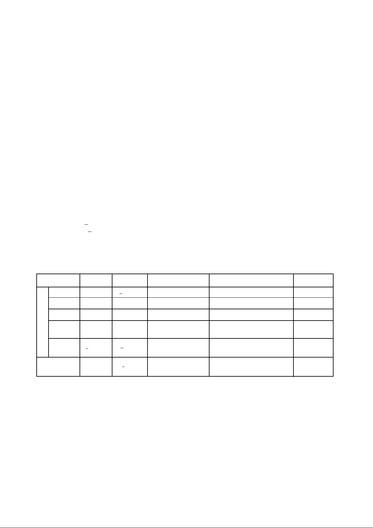
LOCA TION OF CUSTOMER CONTROLS
6
1. Disc tray
This is the tray for the disc. Place the disc on the
ejected disc tray, then lightly push the tray (or
push the eject button) and the CD will be loaded.
NOTE: Don’t pull out or push in the disc tray
forcibly. This might cause damage to the loading
section of the drive.
2. Stop/Eject button
This button is pressed to open the CD tray.
This button works only when power is supplied to
the drive.
If an Audio CD is playing, pressing this button will
stop it, and pressing it again will open the tray.
3. Emergency Eject Hole
Insert a paper clip here to eject the Disc tray
manually or when there is no power.
4. Volume control
This is used to adjust the output volume of the
headphone jack. It can’t be used to adjust the
output volume for the audio output connectors on
the rear panel.
NOTE : Turn the volume down before turning on
the power. Sudden loud noises can damage your
hearing.
5. Headphone jack
This jack is for connecting headphones or minispeakers.
6. Drive activity indicator
Two colored LED is used to indicate the operation
of CD-R/RW Drive.
Headphone Jack
Volume
Control
Drive Activity Indicators
Stop/Eject Button
Disc Tray
Emergency Eject Hole
Front Panel
Page 7
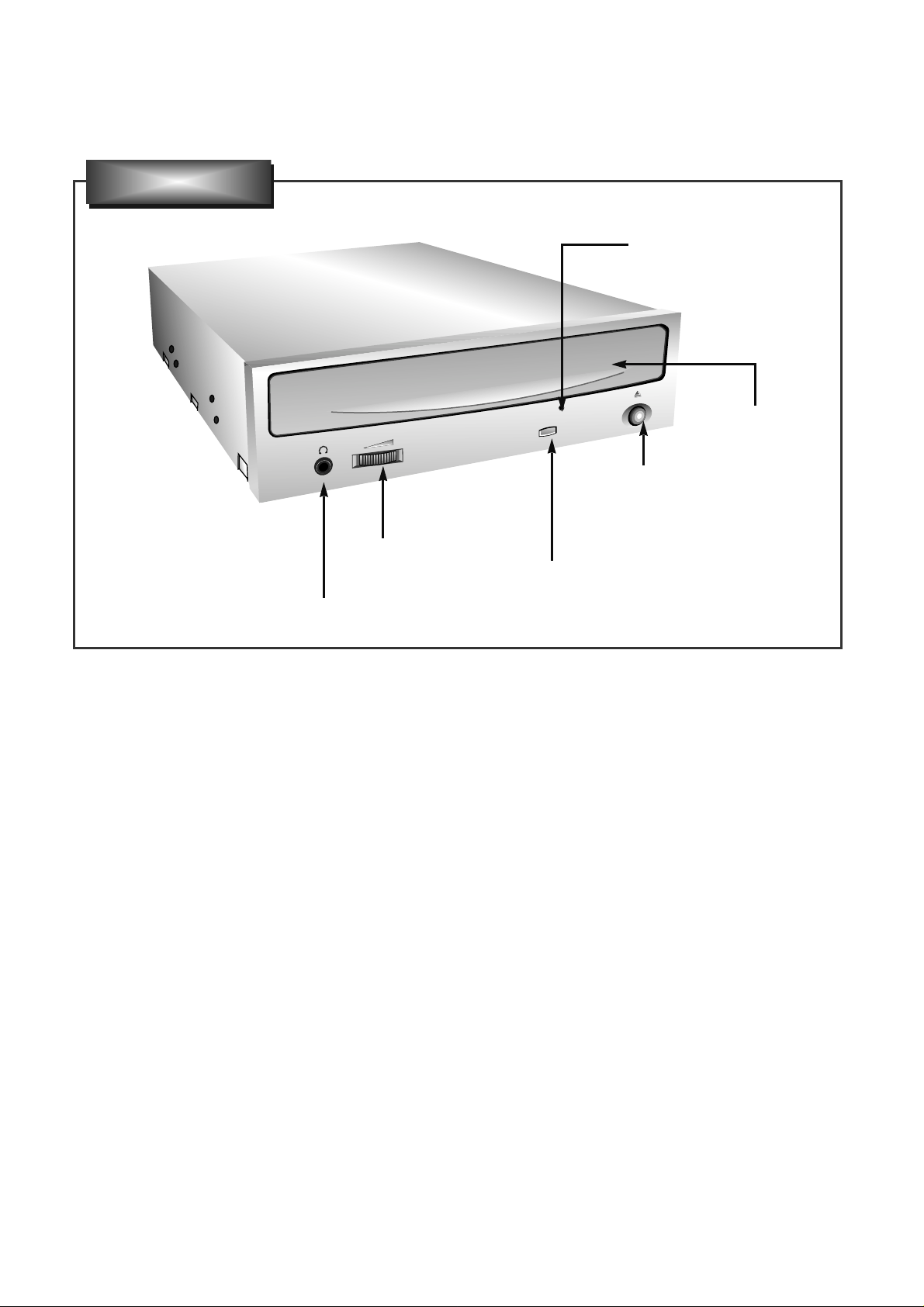
7
1. Power Connector
Connects to the power supply (5-and 12-V DC) of
the host computer.
NOTE : Be careful to connect with the proper
polarity. Connecting the wrong way may damage
the system (and is not guaranteed). Usually this
connector can only be attached one-way.
2. IDE Interface Connector
Connect to the IDE (Integrated Device
Electronics) Interface using a 40-pin flat IDE
cable.
NOTE : Do not connect or disconnect the cable
when the power is on, as this could cause a short
circuit and damage the system. Always turn the
power OFF when connecting or disconnecting the
cable.
3. Jumper Connector
This jumper determines whether the drive is
configured as a master or slave. Changing the
master-slave configuration takes effect after
power-on reset.
4. Analog Audio Output Connector
Provides output to a sound card (analog signal).
Generally you need this to play a regular audio
CD.
5. Digital Audio Output Connector
Provides output to a sound card (digital signal).
DIGITAL
AUDIO
ANALOG
AUDIO
INTERFACE
POW
ER
D G
39
40
1
+5
GND
+12
2
C S M
S L A
R G L
Digital Audio Output
Connector
Jumper Connector
Analog Audio Output Connector
IDE Interface Connector
Power Connector
Rear Panel
Page 8
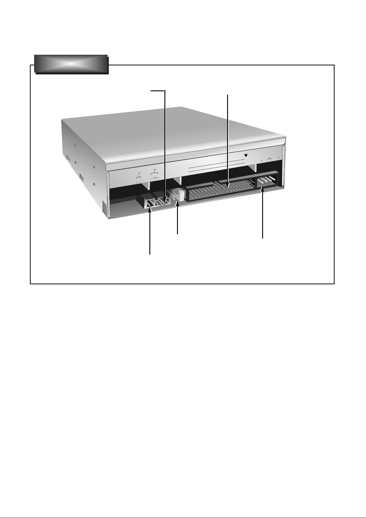
1. CABINET and CIRCUIT BOARD
DISASSEMBL Y
1-1. Bottom Chassis
A. Release 4 screws (A) and remove the Bottom Chassis
in the direction of arrow (1). (See Fig.1-1)
1-2. Front Bezel Assy
A. Insert and press a rod in the Emergency Eject
Hole and then the CD Tray will open in the direction
of arrow (2).
B. Remove the Tray Door in the direction of arrow
(3) by pushing the stoppers forward.
C. Release 3 stoppers and remove the Front Bezel Assy.
1-3. Cabinet and Main Circuit Board
A. Remove the Cabinet in the direction of arrow (4).
(See Fig. 1-3)
B. Release 2 hooks (a) and remove the CD Tray
drawing forward.
C. Remove the Main Circuit Board in the direction of
arrow (5).
D. At this time, be careful not to damage the 4
connectors, are positioned at left and bottom sides,
of the Main Circuit Board.
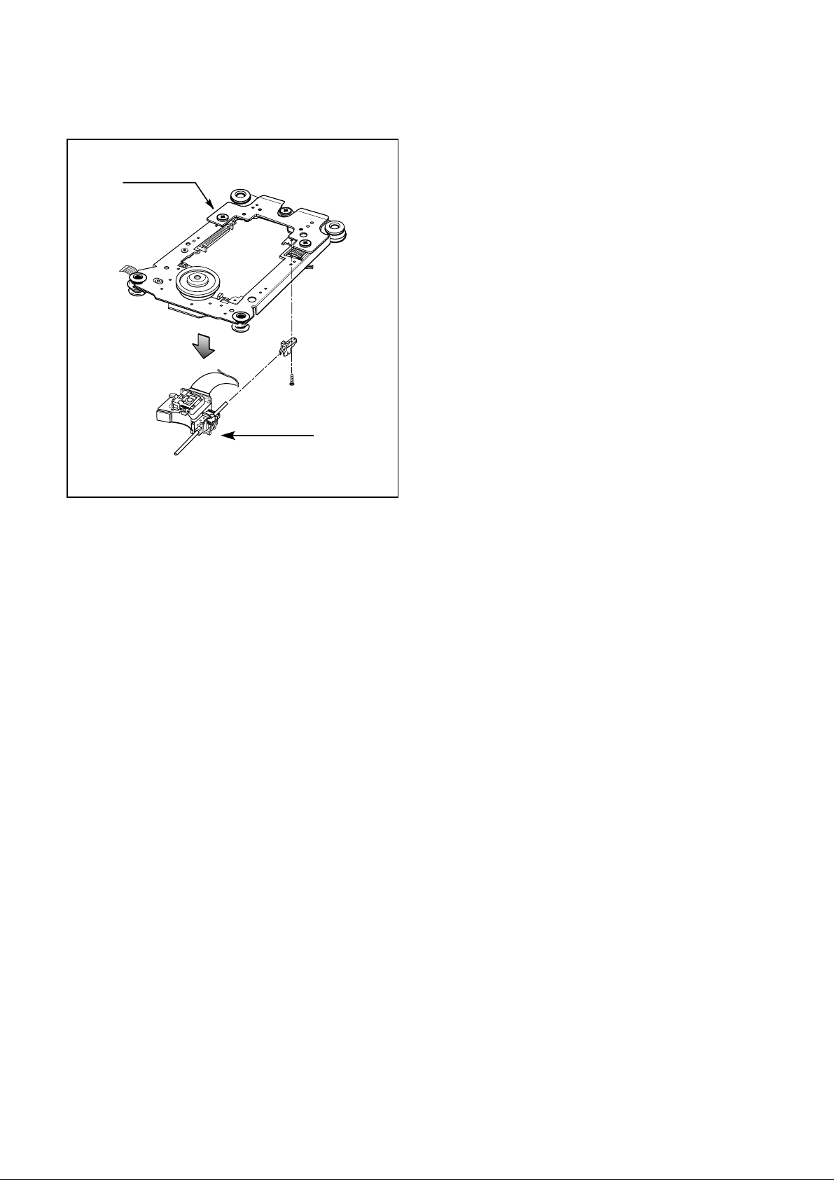
2. MECHANISM ASSY DISASSEMBL Y
2-1. Pick-up Unit
A. Release screws (B).
B. Separate the Pick-up Unit in the direction of arrow (6).
Main
Circuit Board
Cabinet
(4)
(5)
Hooks (a)
Fig. 1-1
Fig. 1-2
DISASSEMBLY
8
Fig. 1-3
Mechanism Assy
Pick-up Unit
(B)
(B)
(6)
Fig. 2-1
(1)
(A)
Bottom Chassis
(A)
(A)
(A)
Tray Door
(3)
Front Bezel Assy
CD Tray
Stoppers
Emergency Eject Hole
(2)
Page 9
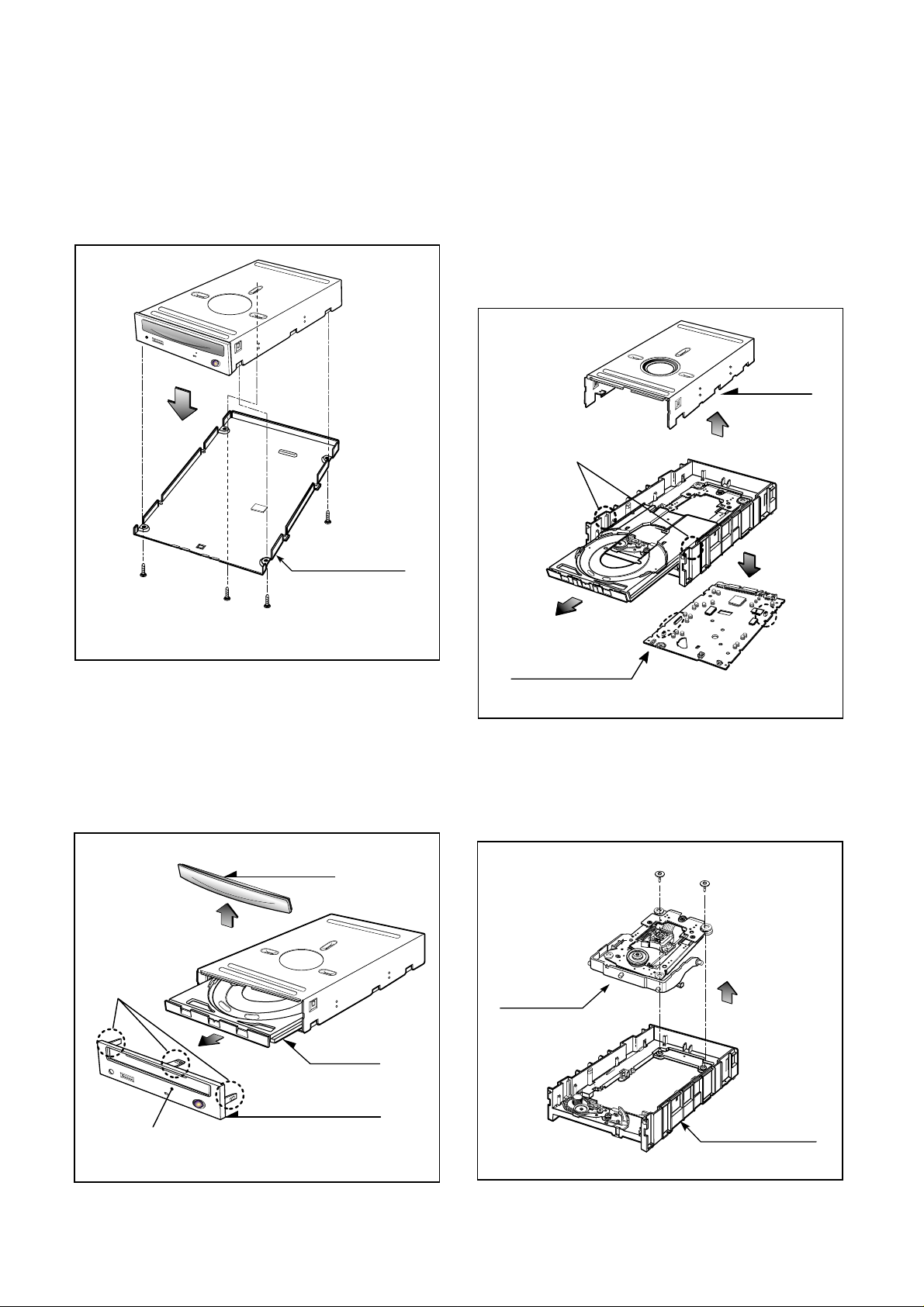
2-2. Pick-up
A. Release 1 screw (C) and remove the Pick-up.
Pick-up Unit
Pick-up
(C)
Fig. 2-2
9
Page 10
030
PBM00 (MAIN C.B.A)
007
A02
A01
021
028
401
032
401
020
021
050
400
022
413
413
413
001
413
430
010
009
420
008
011
012
005
035
016
015
004
006
A B C D E F GH
1
2
3
4
5
003
002
013
452
029
031
027
026
033
025
430
419
020
449
023
014
11 12
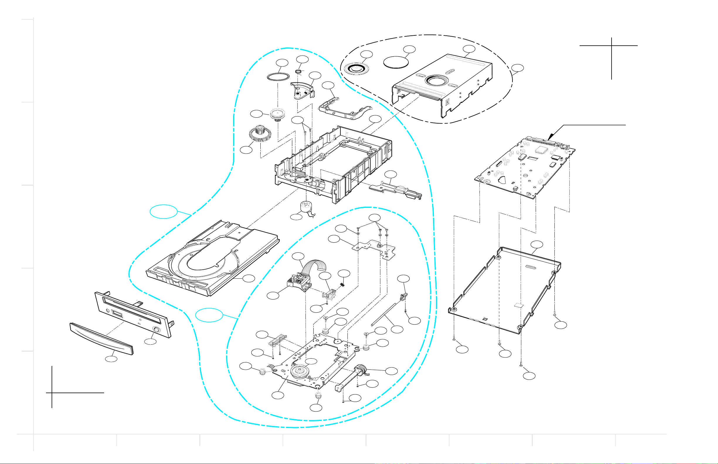
EXPLODED VIEW
Page 11

ATIP Absolute Time in Pre-groove. With an additional modulation of the “Wobble”, the “Groove” contains a time
code information.
Wobble The pre-groove in the Disc is not a perfect spiral but is wobbled.
With : – A typical amplitude of 30 nm
– A spatial peried of 54~64 µm
CW Continuous Wave. The laser light output is at a constant level.
DOW Direct Over-Write. The action in which new information is recored over previously recorded information in
CD-RW disc.
Overwrite
The action in which new information is recorded over previously recorded information.
(Pre-)Groove
The guidance track in which clocking and time code information is stored by means of an FM
modulated wobble.
Land Land is characterized in the following way:
When radial signals are concerned,land is defined as the area between the grooves.
When HF signal are concerned,land is defined as the area between the marks(pits) in tangential
direction.
Hybrid Disc A Multisession disc of which the first Session is mastered. On a hybrid disc, recorded and
mastered information may co-exist.
Mastered Information,stored as pits on the disc during the manufacturing process of the disc.
Information (when making the master)
OPC Optimum Power Control. Procedure is determined optimum recording power according to CD-
R/RW Media in recording start step.
ROPC Running OPC. The purpose is to continuously adjust the writing power to the optimum power
that is required.
When the optimum power may change because of changed conditions of disc and change in
operating temperature.
Jitter The 16 value of the time variation between leading and trailing edges of a specific (I3 … I11) pit
or land as measured by Time Interval Analysis.
Deviation The difference between a fixed value of Pit length and Land length.
TOC Table Of Contents : in the Lead-in Area the subcode Q-channel contains information about the
Tracks on the disc.
Packet A method of writing data on a CD in small increments.
Writing Two kinds of packets can be written : Fixed-length and Variable-length.
Write The shape of the HF write signal used to modulate the power of the laser.
Strategy The Write Strategy must be used for recordings necessary for disc measurements.
Information Wobble, ATIP, Disc Identification, Write Power, Speed Range OPC Parameters, etc are
Area recorded in the Information area of CD-RW Disc
Finalization The action in which (partially) unrecorded or logically erased tracks are finished and the Lead-in
and/or Lead-out areas are recorded or overwritten with the appropriate TOC subcode.
Logical Erase
A method to remove information from a disc area by overwriting it with an EFM signal containing
mode 0 subcode
A logically erased area is equivalent to an unrecorded
Physical Erase
The action in which previously recorded information is erased by overwriting with a CW laser
output.
After a Physical Erase action, the erased area on the CD-RW disc is in the unrecorded state
again.
Session
An area on the disc consisting of a Lead-in area, a Program area, a lead-out area.
Multi session
A session that contains or can contain more than one session composed Lead-in and Lead-out
GLOSSARY
10
Page 12
15
The differences of CD-R/CD-RW discs and General CD-ROM
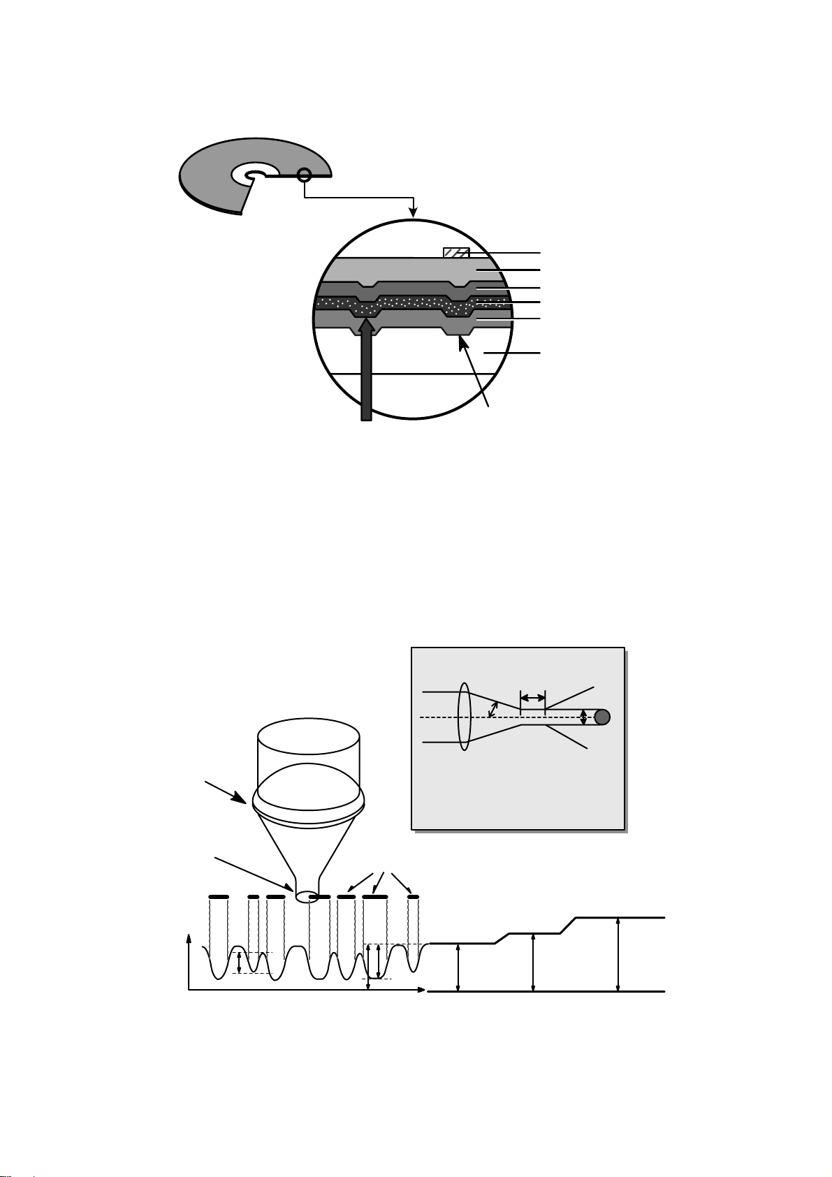
1.Recording Layer
Recordable CD has a wobbled pre-groove on the surface of disc for laser beam to follow track.
2.Disc Specification
Read-only Disc
CD-R and CD-RW Disc
3~1 1T
1.6um
0.4~0.5 um
(Pit)Groove
Land
Track pitch(p)
Radial Direction
Iw
A
O
a
a
Groove
Land
Radial Error Signal
The Groove wobble
Average center
Actual center
CD-ROM (READ-ONLY DISC)
a=30nm
ITEM CD-ROM CD-R CD-RW
Standard Yellow Book Orange Book II Orange Book III
Record Not available Write once Re-Writeable
Tracking Signal I11/Itop > 0.6 > 0.6 0.55 > M11> 0.70
(HF Modulation)
Read Laser Power(mW) < 0.5 mW < 0.7 mW < 1.0 mW
Jitter < 35 nsec < 35 nsec < 35 nsec
Reflectivity (R
top) 70 % 65 % 15 % ~ 25 %
Remark)
Write Laser Power(mW) 14-65 mW 6-45 mW
Page 13
16
3.Disc Materials
1) CD-ROM disc
Laser Beam
Groove
Substrate
(Polycarbonate)
Organic Dye Layer
Reflective Layer
Protective Layer
Label Printing
2) CD-R disc
Pigment Reflective Layer Color
Phtalocyanine Gold/Silver Yellow/White
Cyanine Gold/Silver Dark Green/Bright Green
Azo Gold/Silver Dark Blue
• It is composed of Silver _ colored aluminum plate and Reflective layer.
• Groove (Pit) of aluminum plate make a track.
• Laser wavelength : 780 nm, Laser Power (Read): 0.5mW
• Signal is detected by the
difference of reflective beam
intensity between “pit” and
“Land” on the disc.
• It is so-called WORM (Write Once Read Many) CD.
• It is composed of polycarbonate layer, Organic dye layer, Reflective layer, and Protective
layer.Gold/Silver Reflective layer is used to enhance the reflectivity
• According to the kinds of Organic dye layer, it is divided by Green CD, Gold CD, Blue CD.
• Laser Wavelength : 780 nm, Laser Power (read) : 0.7 mW
• Recording Power : 8x(14~20mW), 16x(25~35mW), 32x(40~50mW), 40x(45~55mW), 52x(50~65mW)
• When some part of dye layer is exposed to laser heat, it’s color changs black.Therefore, writing and
reading is enabled by the difference of reflectivity between changed part and unchanged part.
• Polycarbonate layer has Pre_Groove which make a Track.
Laser Beam
Pit
Substrate
(Polycarbonate)
Reflective Layer
Protective Layer
Label Printing
Page 14
17
3) CD-RW Disc
4.
Reading process of Optical Disc
Laser Beam
Groove
Substrate
(Polycarbonate)
Recording Layer
Dielectric Layer(TL)
Dielectric Layer(UL)
Protective Layer
Label Printing
• It is composed of polycarbonate layer, alloy(silver, arsenic) layer, aluminum reflectivity layer, protective layer.
• An crystalized alloy layer is transformed into noncrystalized by the laser heat. Therefore, writing and reading
is enabled by the difference of reflectivity.
• It is possible to overwrite about 1000 times.
• Laser Wavelength : 780 nm, Laser Power (Read) : 1.0mW
• Recording Power : Erase (4~18mW), Write (6~45mW)
• When disc rewriting, new data is overwritten previously recorded data.
• Polycarbonate layer has a Pre-Groove which make a track.
Lens
H
D
Beam
Spot
Focusing
Lens
Laser Spot
at Constant
Read Intensity
Reflected
Light
Signal
Laser Spot
Position
(Time)
Previously Recorded Marks
Groove Land Mirror
I
3
I
top
I
11
I
G
I
L
I
0
Numerical aperture: NA=nsinθ,
n: Refractive index
Focus depth : H =
λ
/NA
laser spot diameter : D =
λ
/NA
2
θ
Page 15
18
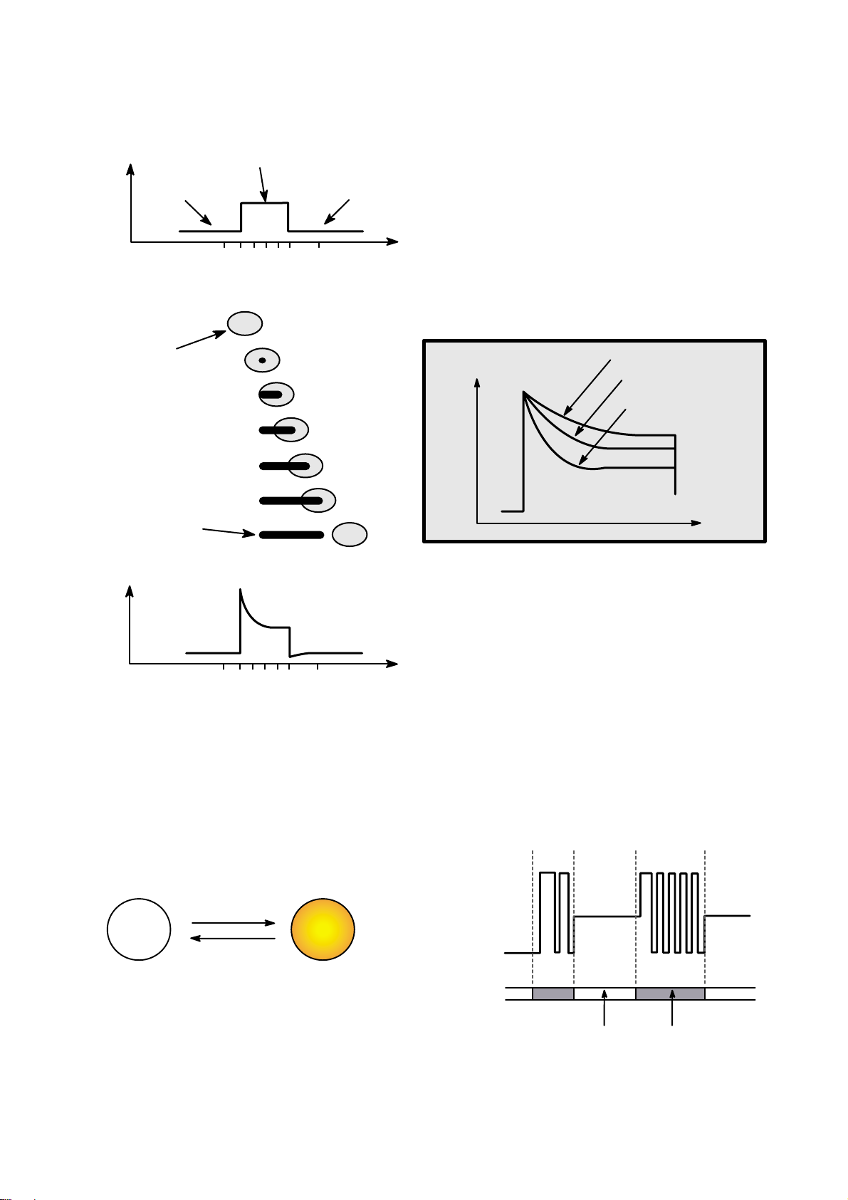
5.Writing Process of CD-R Disc
a b c d e f g
a
b
c
d
e
f
g
Incident
Laser
Power
(Read)
(Read)
(Write)
Laser Spot
Position
(Time)
a b c d e f g
Laser Spot
Position
(Time)
Laser
Spot
Recorded
Mark
Reflected
Light
Signal
Reflected
Light
Signal
Below "ORP"– Mark Too Short
At Optimum Record Power ("ORP")
Above "ORP" – Mark Too Long
Time
6.Writing process of CD-RW Disc
Write Power
Erase Power
Read Power
Groove
Crystal
Amorphous
Amorphous
Recorded state
(lower reflectivity)
Melting/
quenching
Heating/
gradual cooling
Crystal phase
Erased state
(higher reflectivity)
Page 16
19
7.Organization of the PCA, PMA and Lead-in Area
1) Layout of CD-ROM disc
Center hole Clamping and Label Area Information Area
Lead-in Area
Lead-in Area
Diameter 15 mm
Diameter 46 mm
Diameter 120 mm
Program Area
Read Only Disc
Lead-out Area
Program Area Lead-out Area
Center hole
Clamping and Label Area
Information Area
PCA PMA
Test Area Count Area
Diameter 15 mm
Diameter 45 mm
Diameter 120 mm
Unrecorded Disc
Tsl-00:35:65 Tsl-00:15:05
Tsl-00:13:25
Tsl
99:59:74
00:00:00
in out
Test Area : for performing OPC procedures.
Count Area : to find the usable area immediately in T.A
Tsl : start time of the Lead-in Area, as encoded in ATIP
PMA : Program Memory Area
Disc Center
Disc Center
2) Layout of CD-R/RW disc
Page 17
20
8. Function of PCA and PMA area
1) PCA (Power Calibration Area)
• PCA area is used to determine the correct Laser Power for a disc.
– Method 1 : PCA area is divided by a track.
– Method 2 : The previous Calibration value is referred.
– Method 3 : ROPC is used to determine Laser Power value automatically in data writing.
• CD-R Disc can write maximum 99 Tracks but CD-RW Disc can write unlimited tracks because it has a rewritable
function.
2) PMA (Program Memory Area)
• It has a track information (track No, track Start/End time) of every track before writing completed.
– PMA area has the last written point and the next writable point of a disc.
– In case of CD to CD copy, some writer may not write PMA area.
* When Disc is Finalized,
PMA information is transferred to the Lead_In area so that general Driver can read it.
* Because PCA and PMA area exist before Lead-In area, General CD Player or CD-ROM Drive can’t read
these areas.
9. OPC and ROPC
1) OPC (Optimum Power Control)
• This is the first step of writing process, because CD writer has its own laser power value and media have different
writing characteristics,
– This is determined by the Writing characteristic, speed, temperature, and humidity.
– Laser wavelength is determined by the environmental temperature (775~795nm) and Optical Laser Power is
determined by the test and retry.
• Asymmetry and optimum writing Power
– EFM signal Asymmetry is determined by the writing power.
Therefore, Optical Power which has the same value to the preset power value can be estimated by measuring
HF signal Asymmetry on the PCA area.
• Measurement of Asymmetry
* Parameter setting (Beta) : Using AC coupled HF signal before equalization
Beta = (A1+A2)/(A1-A2)
Time
P << Po
Time
P = Po
HF Signal
A1
0
A2
Time
P >> Po
Page 18
21
2) ROPC (Running Optimum Power Control)
• Variable primary factor of Optimum Power
– Change of Power sensitivity on the Disc. (limited to 0.05 *Po)
– Wavelength shift of the laser diode due to the operating temperature change.
– Change of the Spot aberration due to the Disc skew,
Substrate thickness, Defocus.
– Change of Disc or Optics conditions due to the long term OPC
==> It is necessary to adjust continuously to obtain the Optimum Power.
• Principle of Running OPC
– To meet the factors mentioned above,
a horizontal _ direction movement of a curve is uesd.
– Beta = f(B-level) = constant on the Recorded Disc
– Procedure of ROPC
a. Reference B-level is determined during OPC Procedure.
b. During Recording, B-level value is controlled to have a close
Reference B-level value.
c. Normalization of B-level is used to eliminate the effect of reflectivity fluctuation.
==> The reflected B-level value is normalized by the disc reflectivity itself.
CD-R/RW Media
Write Strategy
Determination
PCA Test Area
Program Area
PMA Area
Lead-In Area
Lead-out Area
OPC
PCA Count Area
ROPC
* Recording Capacity of CD-R/RW (74Minute Recording media)
• (2048 Byte/Sector) X (75 Sector/Second) X (60 Second/Minute) X 74 Minute
= 681,984,000 Bytes = 682 Mbytes
• But the actual recording capacity is about 650 Mbytes. (according to the ISO 9660 standard, approximately
30 Mbytes are used to make directory structure and volume names.)
Incident recording pulse
Reflected recording pulse
Sampled timing B
11T
Sample B-level (Write Power)
Level B
Sampled at timing B
Pwo decided by OPC
Recording Power
Level B with Pwo
normalized to recording power
Sample Disc Reflectivity
(Read power)
10. Writing Process of DISC
Page 19
22
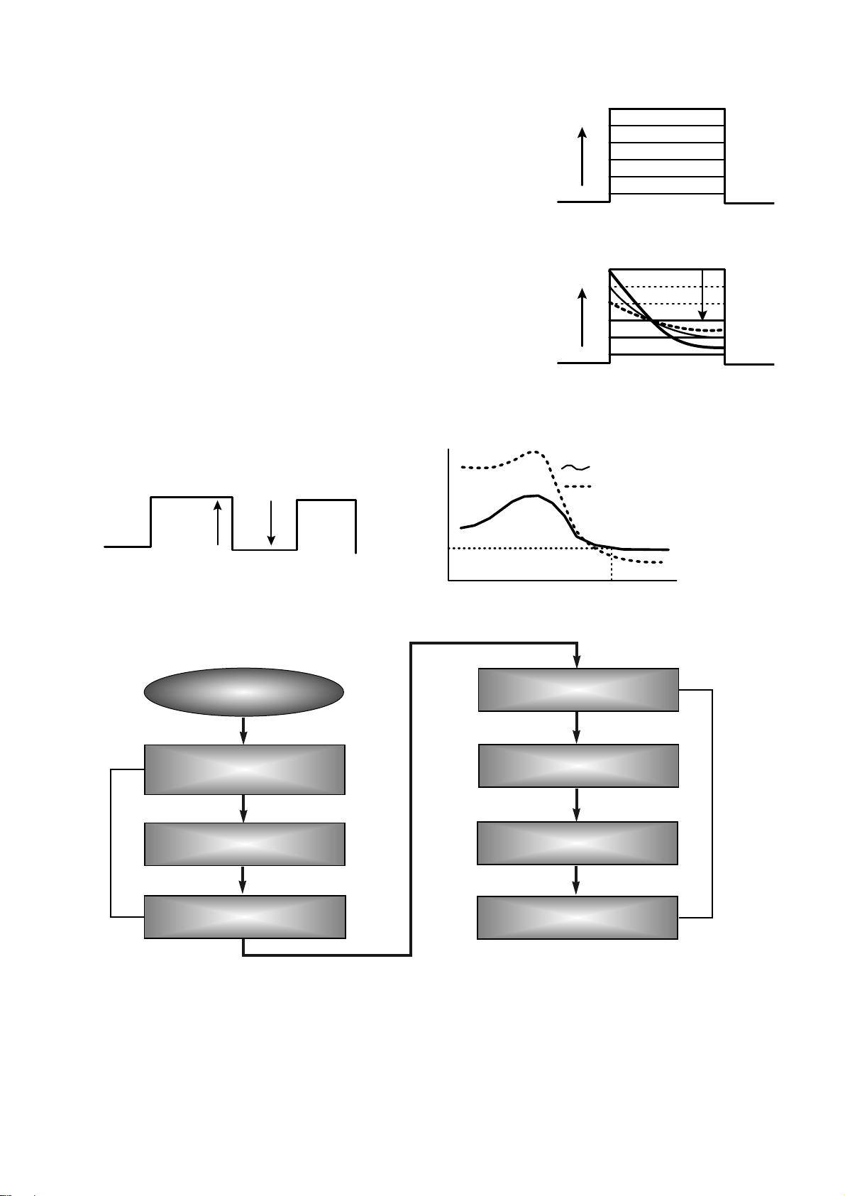
11. Super Link
Super(SUPpressed Error Recording) link method is a new technology to link the interrupted recording by buffer
under run. When drive¡fls buffer will be under, the drive will stop recording and store the stop position. When
drive¡fls buffer receive data from HOST again, the drive will seek to the stop position of last recording and
continue writing. In the read procedure, the drive can not find any error in the linking area, the data or audio will
be regenerated perfectly.
12. Partial CAV Recording
Intial RPM of 52x Full CAV Recording has been considered as 10,200 RPM, 20x to 52x.
13. Optimum record speed
1. All media do not support 52 x Record by media quality.
Even though a CD-R can be recorded by 52x, there is a possibility to occur recording fail during record,
especially in high speed write. Before recording, Drive decides write speed by test. During the high speed
write, Drive checks the record status and control the optimum record speed not to occur record fail. We call
it as ‘Optimum record speed’.
2. During the record, Drive check the ATIP and Servo error. Drive thinks the current record status is unstable,
stops record and decreases a record speed for getting stable record.
( 52x ---> 40x ---> 32x ---> 24x )
1. Micro processor calculates RPM of
Spindle motor by FG signal comes from
Drive IC.
2. Partial CAV : Reference Speed : 52X,
40X, 32x
3. The position of CAV mode is changed
CLV mode, RPM will be reduced.
4. The write power between each
recording speed is changed.
Data
Transfer
Rate
20x
CAV
52x CAV
40x PCAV
32x PCAV
Time
52x CAV
40x PCAV
32x PCAV
0
24min 47min 80min Time
RPM
10,200
8000
Page 20
23
DVD & CD DATA PROCESSING
1.Data Processing Flow
Command
Data
Status
RF EQ & AGC
SERVO
DSP
Encoder & Decoder & CSS
RF data slice EFM demodulator
CiRC error correction
Audio DAC
C3 decoder
Buffer/Memory controller
CSS controller
Atapi interface control
Data PLL
Servo ADC
Focus/tracking
control output
Sled control output
CAV Spindle control
P-up
Unit
IC200
RF AMP
(MT1616E)
CD
DVD
IC100
(MT1618E)
TE/CSO GEN
FE GEN
IC500 DRAM
Flash ROM
IC100
(MT1628E)
Page 21

24
MT1628E
HOST DVD
PLAYER
(MPEG2 B/D)
Scrambled MPEG Data
Change the "KEY"
KEY Management Control
2. Copy Protection and Regional Code Management Block
Block Diagram
Brief Process
1. Regional Code for DVD Disc
– DVD-ROM drive transfers the regional code of the control data to host by the command of host, the DVD
player of host reads the regional code, and plays title in the case of allowed regional code only.
2. Management of DVD Disc for the scrambled of data
(1) DVD-ROM and DVD player of host generate the “KEY 1” respectively, transfer to opposite part, the
“KEY 2” is received, recognizes the data transfer or not with this value, and generates the bus key
encoded the data.
(2) Encoded “Disc Key” and “Title Key” host is transfer with the bus Key.
(3) DVD player of host reads the key value, and uses the value to restore the scrambled data.
* Refer to the next page for the details.
Page 22

25
3. About Prevention the DVD-ROM from to be copy
A data is able to encode and record in the disc, if a copyright holder wants to prevent the disc from copying.
In case of a disc enhanced movie of 3 titles......
DISC KEY (2048 Bytes) is used to encode the whole contents in the disc and TITLE
KEY (5 Bytes) is used to encode the title respectively.
So, the data is encoded and stored in a disc through the unknown algorithms
with a disc key and title key. (At this time, the disc key and title key are stored
in a disc.)
…As above, the disc is able to copy when the disc key and title key are
opened.
Then, ROM-DRIVE encodes the disc key and title key and transfers to MPEG2 board.
If you want to play the disc prevented from the copy......
First of all, ROM-DRIVE and MPEG-2 board identify with each other through the procedure as described
below.
1. Drive and host gives and takes the ID of 2bit. This ID is AGID (Authentication Grant ID).
The various decoder boards are attached to the host, in these, AGID sets the MPEG-2 board and drive.
2. After the AGID is set, MPEG-2 board generates the challenge key (10 Byte) and transfers to drive. The
board and drive generate key 1 (5Byte) with the challenge key respectively. (Of course, the Algorithm
generating the key 1 is not known.)
3. Compare with the generated key 1, if it corresponds each other, the first step of authentication is
completed. This is a course to identify the MPEG-2 board with a drive.
4. The second step of authentication is a course to identify a drive with the MPEG-2 board.
The dirve generates a challenge key and transfers it to the MPEG-2 board. The dirve and MPEG-2 board
generate the key 2 (5Byte) with the challenge key, compare with each other, and if it corresponds and the
secondary step of authentication is completed.
5. As above, the identification is completed.
6. The dirve and MPEG-2 board generate the Bus key with the key 1 and key 2 and own it.
7. Dirve encodes the disc key and title key with this Bus key and transfers to the MPEG-2 board.
8. The MPEG-2 board reads the encoded disc key and title key with the Bus key only.
9. MPEG-2 board lets data read from the drive to decode with the read disc key and title key and makes into
the video signal by decoding.
ROM-DRIVE
AGID
HOST
MPEG-2
BOARD
Challenge key
encoded disc key, title key
Page 23

26
4.About the DVD-ROM Regional Code
DISC ROM - DRIVE MPEG-2 BOARD VGA CARD
MONITOR
1
CAN
U.S.A
MIX
CUB
BHS
PRI. VIR
1
BMG
GRL
2
2
ZAF
ISO
SWZ
FIN
POI
FST
LTU
BIR
UKR
TUR
FGY
JRN
TKM
AFG
PAK
CHN
MMR
MNG
RUS
KOR
JPN
HKG
MAC
TWN
PHL
6
3
2
1
5
5
4
1
MDI
MNP
GUM
PLW
PNG
NZL
AUS
4
The disc has
the regional
code of 8 bit.
Example)
The disc
manufactured
in the U.S.A,
has the
number one.
Transfer to
MPEG-2 board
reading the
regional code.
Receiving
data from the
MPEG-2
board and
output
through the
monitor
If the board is setting to the regional
code 1 for the U.S.A. ...
Check the received regional code to
number 1, all or not, transfer the
data to VGA card in accordance with
only a case among the three case.
Regional code
Page 24

INTERNAL STRUCTURE OF THE PICK-UP
1.Block Diagram of the PICK-UP
27
ACZ1007Y-301-B
L1
C14
38k
VR2
DW
C
A9
R13
R12
R11
R10
R5R4R3
R2 2.2K
2.2K
2.2K
2.2K
O
O
O
O
A3
RF- SW
RF+ EF3
EF2 C
BVC
A VCC
EF1 D
EF4 GND
PH974
78
91011
12
13
14
C11
C4 C5 C6 C7
C9
CD LD
G
A2
LD PD
C10
1n
R8
R9
NCP15XH1D3J03
O
R7
C8
3.9K
0.1u
R6
AK8911
PNA4SB7F
ACTUATOR
TILT- J1-40
TILT+ J1-39
T- J1-38
T+ J1-37
F- J1-36
F+ J1-35
GND(FM) J1-34
FM J1-33
VREF(FM) J1-32
OSCEN J1-31
ENABLE J1-30
EDIS J1-29
RDIS J1-28
W2DIS J1-27
W1DIS J1-26
GND(LD_HF) J1-25
W2SET J1-24
W1SET J1-23
ESET J1-22
RSET J1-21
TEMP J1-20
Vcc(HF) J1-19
Vcc(LD, FM) J1-18
VR J1-17
PD J1-16
LD J1-15
Vcc(OEIC) J1-14
GND(OEIC) J1-13
RF- J1-12
RF+ J1-11
EF2 J1-10
B J1-9
A J1-8
EF1 J1-7
EF4 J1-6
C J1-5
D J1-4
EF3 J1-3
SW J1-2
Vc(OEIC) J1-1
A1
A7
220p 220p 220p 220p
2.7K
0.1u
1234567
16151413121110
9
8
DR14
22
R1
VR1
470
CW
RDIS EDIS
RSET VDD
ESET LD
FADJ VSS
W1SET AADJ
W2SET ENABLE
W1DIS OSCEN
W2DIS
GND
34
25
1
C3C2
0.1u 0.1u
6
IVOT
VREF IN
VCC OUT
VOD
0.1u
0.1u
C12
65432
1
R15
o
3
A8
HFM-1001
4
GND
VCC
GND GND
LD
GND
5
6
2
1
C13
0.1u
DVD LD
LD
PD
0.1u
Page 25

2.Pick up Pin Assignment
28
No. Signal Name I/O Signal Description
1 Vc(OEIC) I reference voltage input for OEIC (+2.3V)
2 SW I gain swich for signal OEIC output (Gain 8.7dB)
3 EF3 O signal OEIC output EF3
4 D O signal OEIC output D
5 C O signal OEIC output C
6 EF4 O signal OEIC output EF4
7 EF1 O signal OEIC output EF1
8 A O signal OEIC output A
9 B O signal OEIC output B
10 EF2 O signal OEIC output EF2
11 RF+ O signal OEIC output RF+
12 RF- O signal OEIC output RF13 GND(OEIC) ground connection for OEIC
14 Vcc(OEIC) I Power supply for HF signal and OEIC
15 LD I input current for driving Laser Diode
16 PD O output current of Laser Diode power monitor for APC amplifier
17 VR O output voltage of controlling signal level of Laser Diode for APC
18 VCC(LD.FM) I power supply for LD (+5V) and FM
19 VCC(HF) I power supply for HF (+5V)
20 TEMP O output voltage for controlling temperature
21 RSET I input voltage for current amplifier
22 ESET I input voltage for current amplifier
23 W1SET I input voltage for current amplifier
24 W2SET I input voltage for current amplifier
25 GND(LD, HF) ground connection for LD-IC and HF signal
26 W1DIS I Digital control of channel W1SET (low active)
27 W2DIS I Digital control of channel W2SET (low active)
28 RDIS I Digital control of channel RSET (low active)
29 EDIS I Digital control of channel ESET (low active)
30 ENABLE I Enables output current (high active)
31 OSCEN I Oscilator shutdown (OSCEN Low=oscillator off, Floats Low)
32 VREF(FM) I reference voltage input for FM
33 FM O APC amplifier output
34 GND(FM) ground connection for FM
35 AF+ I focusing Actuator drive signal +
36 AF- I focusing Actuator drive signal 37 TR+ I tracking Actuator drive singal +
38 TR- I tracking Actuator drive signal 39 TILT+ I Tilting Actuator drive signal +
40 TILT- I Tilting Actuator drive signal -
ENBLE RDIS EDIS W1DIS W2DIS
0XXXX
11111
10111
11011
11101
11110
ENBLE RDIS EDIS W1DIS W2DIS OSCEN OSCILATOR
0XXX XXOFF
1 1 1 1 1 X OFF
1000 00OFF
1000 01 ON
IOUT CONTROL
OSCILLATOR CONTROL
X : Don’t care
Page 26

3.Signal detection of the P/U
1) Focus Error Signal ==> (A+C)-(B+D)
This signal is generated in RF IC (IC200 : MT1616E) and controls the pick-up’s up and down to focus on
Disc.
2) Tracking Error Signal (DPP Method) ==> {(A+D)-(B+C)}- k x {(EF1+EF4)-(EF2+EF3)}
This signal is generated in RF IC (IC200 : MT1616E) and controls the pick-up’s left and right shift to find
to track on Disc.
3) RF Signal ==> (A+B+C+D)
This signal is converted to DATA signal in DSP IC (IC100 : MT1628E).
29
Pick-Up module
Photo Diode
Tracking
Focusing
Infrared Iaser
k[(F+H) - (E+G)]
(A+D) - (B+C)
(A+D) - (B+C) - k[(F+H) - (E+G)]
Offset
TE
Tp
Sub2
Main
Tp/2
Sub1
T rac k Center
F,E
D,C
A,B
H,G
Page 27

DESCRIPTION OF CIRCUIT
1. ALPC (Automatic Laser Power Control) Circuit
1-1. Block Diagram
30
MT1628E
Write
Strategy
Write
S/H Signal
Micro
Processor
IC 100
CN 101
IC200 (
MT1616E)
Optical
Pick-up
LPC-711A
LD
Drive
33 114
113
FPDO
FPDOLP
10523
VWDC1O
VWDC1
10624
VWDC2O
VWDC2
61 177
WLDON
59
179
RLDON
10421
VRDCO
RREF
VRDC
58
181
RFPDSH
S/H &
VRDCG &
Level Shift
60
S/H &
VWDC1G &
Level Shift
VWDC1
DAC
& Gain
WFPDSH
178
WDAC2
&
Amplifier
WDAC1
& x1/x2
RDAC
VRDC
DAC
& Gain
32 112
FVREF
+
-
-
+
1-2. APC (Automatic Power Control) Block
APC (Automatic Power Control) function in CD-R/RW analog front-end is used for constant power level control
purpose. Based on the accurate power sensor (FMD) in PUH, APC feedback loop maintains constant power level against
laser diode’s temperature variation.
There are three power control loops in MT1616, two for CD and one for DVD, which are used with different combination
for different applications. Generally, the first APC loop is used for read-power control. The second APC loop is used for write
(erase) power control for CD-R (CD-RW) disc. And the third APC loop is used for DVD read power control.
Owing to the small signal level in read-power control mode, the first APC loop amplifies (x5/x10/x15/x20) the FMD
signal (FPDO) to enhance the accuracy of read power control. The register VRDCG[1:0] is used to adjust the gain of FMD
signal. The registers RDAC[7:0] and VBDAC[7:0] will set the read power level at the built-in 8-bit DAC (RDAC). The second
APC loop is used for high power control. The built-in 10-bits DAC(WDAC1) is used to set the wanted power level. And the
register VWDC1G is employed to adjust the gain of FMD signal.
The following potentiometers (VRDCDAC, VWDC1DAC, and VWDC2DAC) and amplifiers (VRDCDAG, VWDC1DAG,
and WDAC2G) are used to set the wanted levels of VRDCO, VWDC1O, and VWDC2O. Moreover, the input source of the
VWDC2O path can be fed from the output of VWDC1O or directly programmed by the built-in 10-bit DAC (VWDC2DAC).
Moreover, the input signal FPDO (form CD FMD) after low-pass filtering $ amplification (x1 or x2) will send the
MPXOUT2 for monitoring.
Furthermore, the third loop is used for DVD read power control loop. Read power level is adjusted by the RREF voltage
set in the first APC loop.
Page 28

2. Focus/Tracking/Sled Servo Circuit
2-1. Focus, T racking & Sled Servo Process
31
Focus, Tracking Servo
C
B
D
A
F1
F2
F4
F3
E1
E2
E4
E3
Pick- up
A,B,C,D,E, F,G,H
A,B,C,D
Focus Error
Detector
Track Error
Detector
A,B,C,D
E,F,G,H
IC200 MT1616E
FE
TE
TE FE
A/D
PARALLEL
DIGITAL
COMPENSATOR
DAC
SLED
COMPENSATOR
PWM
FMSO
FMSO2
IC100
Servo Control
MT1618E
Tracking x5
Focus x5
Tracking Focus ing
Actuator
FOSO
TRSO
F+
F-
T+
T-
Sled Control
M
Stepping Control
Logic
SL1+
IC300
M63028FP
SL1SL2SL2+
IC300 M63028FP
27 12
28 13
18
14
1
2
MT1628E
Page 29

3. Spindle Servo Circuit
3-1. Spindle Servo Process
3-2. Spindle Servo
Spindle servo is as followings;
1)Wobble CLV x4, x8, x10,x16, x24, x32,x40 : Blank area in CD-R, CD-RW.
2)CD 10x CAV: Eccentric CD-R/RW, Video CD, CD-Audio Analog.
3)CD 40x CAV: Recorded area in CD-R/RW, CD-Adio Digital.
4) CD 52x CAV : CD-ROM
5) DVD 6x CAV: DVD+RW, DVD-R, DVD-RW
6)DVD 8x CAV: Dual Layer DVD-ROM, Single Layer DVD-ROM(Movie)
– Spindle Servo is controlled by IC100(MT1628E) and servo signal is output via DMO (pin 17).
7) DVD 16x CAV : Single Layer DVD-ROM (Data)
32
A
B
DC
E1 E2
E4 E3
F1 F2
F4 F3
Pick- up
IC200 MT1616E
Wobble Signal
Generator
RF
SRF
EFM
WOBSI
Decode PLL
Frequency
Controller
CD-DSP/SERVO
LOCK
DEFS
MOTOR SPEE D
CONTROLLER
174
FILTER
TON
DMSO
ATIP CLV, FG
Level Shift
Hall Sensor
M
Spindle Motor
SPNON
SPNFG
REVDEF
IC100 MT1618E
IC301 HD153704
CD WOBBLE CLV
FG CAV 40X
6
8
IC300 M63028FP
40
65
17
55
6364
MT1628E
48X
Page 30

MAJOR IC INTERNAL BLOCK DIAGRAM AND PIN DESCRIPTION
IC200 (MT1616E) : RF AMP
Pin Assignment
33
ATFG
GIO2
EEP_CS
EEP_SCLK
EEP_SDATA
DRVOUT0
DRVOUT1
DRVOUT2
FR
LIMIT#
LED2
LED1
TRAYIN#
TRAYOUT#
ENBL
GIO1
SUBGND1
AVSS3
AGC3C
AGC2C
AGC1C
AVDD3
AVDD6
VREF
V14
V28
VHAVC
VFVREF
AVSS6
MPXOUT2
MPXOUT1
RRFXLP
AUX1
AUX2
DVDMDI
DVDLDO
VDAC0
VDAC1
OSCL1CP
OSCL1CN
RFAGCI
RFAGCU
RFAGC
EQBIAS
AVSS4
RFON
RFOP
AVDD4
RFIN
RFIP
AVDD7
DVDA
DVDB
DVDC
DVDD
AVSS7
RRFSUM
AVDD5
RRF/WRF
AVSS5
WRFSUM
HTRLP
AVDD1
INA
INB
INC
IND
HAVC
AVSS1
TRINA
TRINB
TRINC
TRIND
INE
INF
ING
38
37
36
35
34
33
32
31
30
29
28
27
26
25
24
23
22
21
20
19
18
17
16
15
14
13
12
11
10
9
8
7
6
5
4
3
2
1
65
66
67
68
69
70
71
72
73
74
75
76
77
78
79
80
81
82
83
84
85
86
87
88
89
90
91
92
93
94
95
96
97
98
99
100
101
102
GIO3
XRST#
WBLCLK
WLDON/IDGATE
WFPDSH
RLDON/UDGATE
RFPDSH
H11T/VF013
DVSS1
MCLK
DVDD1
XLAT
SCLK
SD ATA
ASPREQ
LRFZC/BLANK
DVDD2
SRVSH
HTRC/PHTO
WBLSH
DVSS2
GIO4
RFSUBO
SUBGND2
OSCL2CP
OSCL2CN
AVSS2
VRDC0
VWDC1O
VWDC2O
AVDD2
VRDCN
VRDC
VWDC1N
VWDC1
FVREF
FPDOLP
FPDO
SHBC
SHPC
PHTIN
DFCTLP
SBAD/RFLVL
TEIN
TE
CE
FE
DRCO2
DRCO
FOIN
FOIP
INH
64636261605958575655545352515049484746
45
44
43
424140
39
103
104
105
106
107
108
109
110
111
112
113
114
115
116
117
118
119
120
121
122
123
124
125
126
127
128
MT1616
COMBI RF IC
Page 31

Block Diagram
34
RRFSUM
RRF/WRF
VRDCO
VWDC1O
VWDC2O
VRDC
FPDOLP
RFON
RFAGCI
RFIN
RFIP
RFAGCU
RFAGC
RFOP
EQBIAS
OSCL1CP
OSCL1CN
OSCL2 CP
OSCL2 CN
A
B
C
D
HAVC
SERVO
&
Detection
A
B
C
D
HAVC
GAINUP
RRFXLP
RRFX
GAINUP
A
B
C
D
HAVC
RRF
APC
RFZC1
MCLK
MPX1
MPX2
VCON
RRFX
ADBCO
BC O
ADO
FPDOX
TELP
MPPO
SPPO
DRCO
RFRP
MPX1
TZC
MPX2
MPX1
P/H
B/H
x1
ASH
BSH
DSH
ESH
CSH
FSH
GSH
HSH
MPX2
MPX2B
VRDCB
VWDC1B
WREF1
RREF
WRFSH
AUX1
AUX2
ADBCO
ADO
BC O
SF E O
MPPO
SBADO
SPPO
S/H
&
MATRIX
RECDIN
TE
FE
CE
TESTM2
SBADOLP
VCON
MPXOUT2
MPXOUT1
MPX2B
ATFG
AGC3C
AGC2C
AGC1C
WBLCLK
VREFMPX
TESTM1
D RCSO
DRCMO
RRFX LP
H11T/VFO1 3
ATIP/
Wobble
10-Bit
ADC
SBAD/RFLVL
AUX2
AUX1
WRFSUM
FE
DRCO2
CE
TE
SBAD/RFLVL
TEIN
DEFECT
RFZC1
TZC
DFCTLP
FOIP
FOIN
HAVC
WBLSH
SRVSH
DRCO
MFEO
LRFZC/BLANK
SHPC
SHBC
PHTIN
HTRC/PHTO
HTRLP
VWDC1
VWDC1N
FPDO
FVREF
VRDCN
DVDLDO
DVDMDI
RFPDSH
WFPDSH
RLDON/UDGATE
WLDON/IDGATE
WRF
AVDD1
AVSS1
AVDD2
AVSS2
AVDD3
AVSS3
AVDD4
AVSS4
AVDD5
AVSS5
AVDD6
AVSS6
AVDD7
AVSS7
DVDD1
DVSS1
DVDD2
DVSS2
DVDD
SUBGND1/2
Voltage
Ref & DAC
DPFO
DPFO
DVDC
DVDB
DVDA
TRINA
TRINB
TRINC
TRIND
RFSUBO
DIG.
REG.
ING
INC
INB
INA
IND
INE
INH
INF
DPD
EQRF RRF
ROPC
DEFECT
RFRPLP
ATFMX
FPDO
ADO
DPFO
HRFRP
WRFX
MDG/LDO
GDAC0
HTRL PA
FELP
DFCTIN
HTE
VRDCO
VWDC1O
VWDC2O
BCO
TRAYOUT#
TRAYIN#
LED1
LED2
LIMIT#
FR
DRVOUT2
DRVOUT1
DRVOUT0
EEP_SDATA
EEP_SCLK
EEP_CS
ENBL
ASPREQ
GIO1~GIO4
General
I/O
SDATA
XLAT
SCLK
XRST#
VDA C1
VDAC0
VRE F
VFVREF
V14
VHA VC
V28
Page 32

35
• Pin Description
Pin
Numbers
Symbol Type Description
RF Signals & S/H Control Pulses
9 HAVC Analog Output Decoupling Pin for Reference Voltage of Main and Sub Beams
13 INA Analog Input Input of Main Beam Signal (A)
12 INB Analog Input Input of Main Beam Signal (B)
11 INC Analog Input Input of Main Beam Signal (C)
10 IND Analog Input Input of Main Beam Signal (D)
3 INE Analog Input Input of Sub-Beam Signal (E)
2 IN F Analog Input Input of Sub-Beam Signal (F)
1 IN G Analog Input Input of Sub-Beam Signal (G)
128 INH Analog Input Input of Sub-Beam Signal (H)
27 RFIP Analog Input Differential Input of AC Coupling RF SUM Signal (Positive)
28 RFIN Analog Input Differential Input of AC Coupling RF SUM Signal (Negative)
20 RRFSUM Analog Input DC Input of RRF SUM signal for CD
16 WRFSUM Analog Input DC Input of WRF SUM signal for CD
25 DVDA Analog Input Input of AC coupled DVD RF signal (A)
24 DVDB Analog Input Input of AC coupled DVD RF signal (B)
23 DVDC Analog Input Input of AC coupled DVD RF signal (C)
22 DVDD Analog Input Input of AC coupled DVD RF signal (D)
7 TRINA Analog Input Input of Tracking Signal (A)
6 TRINB Analog Input Input of Tracking Signal (B)
5 TRINC Analog Input Input of Tracking Signal (C)
4 TRIND Analog Input Input of Tracking Signal (D)
127 FOIP Analog Input Input of Focusing Signal (Positive)
126 FOIN Analog Input Input of Focusing Signal (Negative)
47 SRVSH
Digital Input (TTL),
SMT
S/H Control Pulse of Main and Side Beam Signals
45 WBLSH
Digital Input (TTL),
SMT
S/H Control Pulse of Wobble Signal
Focus/Tracking Error & Servo Control Signals
125 DRCO Analog Output Output of Differential Radial Contrast (DRC) Signal
124 DRCO2 Analog Input Re-Input of Differential Radial Contrast (DRC) Signal
123 FE Analog Output Output of Focusing Error (FE) Signal
121 TE Analog Output Output of Tracking Error (TE) Signal
122 CE Analog Output Output of Center Error (CE) Signal
119 SBAD /RFLVL Analog Output
(1). Output of SBAD Signal
(2). RF Level Output
120 TEIN Analog Input Input of Out-of-Track Detection Circuit
118 DFCTLP Analog Output Low Pass Filter Capacitor Connecting for DEFECT Detection
116 SHPC Analog Output External Capacitor Connection for Peak Hold of RFRP Signal
115 SHBC Analog Output External Capacitor Connection for Bottom Hold of RFRP Signal
42 RFSUBO Analog Output Header Push-Pull RF Output Signal
49 LRFZC/BLANK
4 mA Driving
(1). Output of RF Zero Crossing Binary Signal
(2). Output of Blank Signal
117 PHTIN Analog Input Input of Comparator for Photo Interrupt Signal
15 HTRLP Analog Output Low Pass Filter Capacitor Connecting for HTRC Detection
Digital Output (TTL),
Page 33

36
Pin
Numbers
Symbol Type Description
46 HTRC/PHTO
Digital Output (TTL),
4 mA Driving
(1). High Speed Track Counting Digital Output
(2). Output of Photo Interrupt Signal
EQRF Circuits
33 EQBIAS Analog Output External Bias Connection for Circuits in EQRF Block
38 OSCL1CP Analog Output
External Capacitor Connection of Offset Cancellation Loop1 for
VGA in EQRF Block (Positive)
37 OSCL1CN Analog Output
External Capacitor Connection of Offset Cancellation Loop1 for
VGA in EQRF block (Negative)
36 RFAGCI Analog Output RF AGC Loop Capacitor Connecting for DVD-RAM
35 RFAGCU Analog Output RF AGC Loop Capacitor Connecting for DVD-RAM
34 RFAGC Analog Output External Capacitor Connection for RF AGC in EQRF Block
30 RFOP Analog Output Differential Output of RF Signal (Positive)
31 RFON Analog Output Differential Output of RF Signal (Negative)
40 OSCL2CP Analog Output
External Capacitor Connection of Offset Cancellation Loop2 for
Equalizer Output (Positive)
39 OSCL2CN Analog Output
External Capacitor Connection of Offset Cancellation Loop2 for
Equalizer Output (Negative)
RRF & ROPC (Running OPC) Related Signals
18 RRF/WRF Analog Output Output of Read RF (RRF) or Write RF (WRF) Signal
96 RRFXLP Analog Output Low Pass Output of RRF Signal
57 H11T/VFO13
Digital Input (TTL),
SMT
(1). S/H Control Pulse of WRF Signal
(2). DVD-RAM Header Signal
ATIP (Absolute Time In Pre-groove)
85 AGC1C Analog Output External Capacitor Connection of AGC1 in ATIP Block
84 AGC2C Analog Output External Capacitor Connection of AGC2 in ATIP Block
83 AGC3C Analog Output External Capacitor Connection of AGC3 in ATIP Block
65 ATFG
4 mA Driving
Digital Output of Wobble Signal after Slicing
62 WBLCLK
Digital Input (TTL),
SMT
External Clock Input for Wobble BPF (SCF)
APC (Auto Power Control for Laser)
114 FPDO Analog Input Laser Power Monitor Input for CD APC
113 FPDOLP Analog Output Low Pass Output of FPDO Signal
112 FVREF Analog Input Reference Voltage of CD APC Loops
59
RLDON/
UDGATE
Digital Input (TTL)
(1). Laser Diode Control for CD-ROM/R/RW Read Mode
(2). Control Signal for DVD-RAM Read
61
WLDON/
IDGATE
Digital Input (TTL)
(1). Laser Diode Control for CD-R/RW Write Mode
(2). Control Signal for DVD-RAM Read
58 RFPDSH
Digital Input (TTL),
SMT
S/H Control Pulse for CD-ROM/R/RW Read APC
60 WFPDSH
Digital Input (TTL),
SMT
S/H Control Pulse for CD-R/RW Write APC
108 VRDCN Analog Input Vin(-) of Midcourse Amplifier for CD Read APC Loop
109 VRDC Analog Output Midcourse Output of Laser Diode Control in CD Read Mode
104 VRDCO Analog Output Output Voltage of Laser Diode Control in CD Read APC
110 VWDC1N Analog Input Vin(- ) of Midcourse Amplifier for CD-R/RW Write APC
Digital Output (TTL),
Page 34

37
Pin
Numbers
Symbol Type Description
111 VWDC1 Analog Output Midcourse Output of Laser Diode Control in CD-R/RW Write APC
105 VWDC1O Analog Output Output Voltage 1 of Laser Diode Control in CD-R/RW Write APC
106 VWDC2O Analog Output Output Voltage 2 of Laser Diode Control in CD-R/RW Write APC
99 DVDMDI Analog Input Laser Power Monitor Input for DVD APC
100 DVDLDO An alog Output Laser Driver Output of DVD APC
Reference Voltages & DACs
91 VHAVC Analog Output Output of Voltage Reference (2.0V/2.1V/2.2V/2.5V)
88 VREF Analog Output Decoupling Pin for Internal Voltage Reference (2.0V)
89 V14 Analog Output Output of Voltage Reference (1.4V)
90 V28 Analog Output Output of Voltage Reference (2.8V)
92 VFVREF Analog Output Output of Voltage Reference (2.5V/2.7V/2.8V/3.0V)
101 VDAC0 Analog I/O Output General 8-Bit DAC
102 VDAC1 Analog Output Output of General 10-Bit DAC
MPXOUT (Multiplexer Circuit for Various Signals) and Testing Interface
97 AUX1 Analog Input Auxiliary Input 1 for Signal Monitoring
98 AUX2 Analog Input Auxiliary Input 2 for Signal Monitoring
95 MPXOUT1 Analog Output Multiplexer Output 1 for Signal Monitoring
94 MPXOUT2 Analog Output Multiplexer Output 2 for Signal Monitoring
Serial Interface & Other Digital Control Signals
50 ASPREQ
4 mA Driving
ASP Request Signal Output to MT1618 for Sending Control Signals
via Serial Interface.
52 SCLK
Digital Input (TTL),
SMT
Clock Input for Register Setting
51 SDATA
Digital I/O (TTL),
4 mA Driving
Data Input/Output for Register Setting
53 XLAT
Digital Input (TTL),
SMT
Latch Input for Register Setting
63 XRST#
Digital Input (TTL),
SMT
Digital Input for Register Resetting, Active Low.
55 MCLK
Digital Input (TTL),
SMT
Digital Input of Main Clock
77 TRAYIN#
Digital Input (TTL),
50K Pull-Up, SMT
Tray_is_in Input, A Logical Low Indicates the Tray is IN.
Feedback Flag is from Tray Connector.
78 TRAYOUT#
Digital Input (TTL),
50K Pull-Up, SMT
Tray_is_out Input. A Logical Low Indicates the Tray is OUT.
Feedback Flag is from Tray Connector.
74 LIMIT#
Digital Input (TTL),
50K Pull-Up, SMT
Sledge Inner Limit Input, Active Low.
73 FR
Digital Input (TTL),
SMT
Spindle Motor Reverse Detection Input.
76 LED1
4 mA Driving
LED Control Output. Initial 0 Output.
75 LED2
4 mA Driving
LED Control Output. Initial 0 Output.
72 DRVOUT2
4 mA Driving
Motor Drive Control Signal-2. Initial 0 Output.
71 DRVOUT1
4 mA Driving
Motor Drive Control Signal-1. Initial 0 Output.
70 DRVOUT0
4 mA Driving
Motor Drive Control Signal-0. Initial 1 Output.
Digital Output (TTL),
Digital Output (TTL),
Digital Output (TTL),
Digital Output (TTL),
Digital Output (TTL),
Digital Output (TTL),
Page 35

38
Pin
Numbers
Symbol Type Description
67 EEP_CS
Digital Output (TTL),
4 mA Driving
EEPROM Chip Select Output.
68 EEP_SCLK
4 mA Driving
EEPROM Transmit Clock Output.
69 EEP_SDATA
Digital I/O (TTL),
50K Pull-Down,
4mA Driving
EEPROM Transmit Data Input/Output.
79 ENBL
Digital Output (TTL),
4 mA Driving
Laser Diode Enable Signal Output.
80 GIO1
Digital I/O (TTL),
50K Pull-Up,
4 mA Driving
General I/O 1 for Mass Production Use (Initial Input Mode)
66 GIO2
Digital I/O (TTL),
50K Pull-Up,
4 mA Driving
General I/O 2 for Mass Production Use (Initial Input Mode)
64 GIO3
Digital I/O (TTL),
50K Pull-Up,
4 mA Driving
General I/O 3 for Mass Production Use (Initial Input Mode)
43
GIO4
Digital I/O (TTL),
50K Pull-Up,
4 mA Driving
General I/O 4 for Mass Production Use (Initial Input Mode)
Power Supplies
81 SUBGND1 Analog Ground Ground Pin for Substrate Bias of Internal Digital Circuitry
41 SUBGND2 Analog Ground Ground Pin for Substrate Bias of Internal Digital Circuitry
14 AVDD1 Analog Power Power Pin for Internal Analog Circuitry (5V)
8 AVSS1 Analog Ground Ground Pin for Internal Analog Circuitry
107 AVDD2 Analog Power Power Pin for Internal Analog Circuitry(5V)
103 AVSS2 Analog Ground Ground Pin for Internal Analog Circuitry
86 AVDD3 Analog Power Power Pin for Internal Analog Circuitry (5V)
82 AVSS3 Analog Ground Ground Pin for Internal Analog Circuitry
29 AVDD4 Analog Power Power Pin for Internal Analog Circuitry (5V)
32 AVSS4 Analog Ground Ground Pin for Internal Analog Circuitry
19 AVDD5 Analog Power Power Pin for Internal Analog Circuitry (5V)
17 AVSS5 Analog Ground Ground Pin for Internal Analog Circuitry
87 AVDD6 Analog Power Power Pin for Internal Analog Circuitry (5V)
93 AVSS6 Analog Ground Ground Pin for Internal Analog Circuitry
26 AVDD7 Analog Power Power Pin for Internal Analog Circuitry (5V)
21 AVSS7 Analog Ground Ground Pin for Internal Analog Circuitry
54 DVDD1 Digital Power Power Pin for Internal Digital Circuitry (5V)
56 DVSS1 Digital Ground Ground Pin for Internal Digital Circuitry
48 DVDD2 Digital Power Power Pin for Digital I/O Pads Buffer Circuitry (5V)
44 DVSS2 Digital Ground Ground Pin for Digital I/O Pads Buffer Circuitry
Digital Output (TTL),
Page 36

IC100 (MT1628E) : Encoder, Decoder & DSP Signal Processor
Pin Diagram
39
1
2
3
4
5
6
7
8
9
10
11
12
13
14
15
16
17
18
19
20
21
22
23
24
25
26
27
28
29
30
31
32
33
34
35
36
37
38
39
40
41
42
43
44
45
46
47
48
49
50
51
52
53
IREF
PLLVSS
LPIOP
LPIOP
LPFON
LPFIP
LPFIN
LPFOP
JITFO
JITFN
PLLVDD33
FOO
TRO
FMO2
PWMOUT
DVDD25
DMO
FMO
TRAYPWM
FG
DVSS
EJECT#
PLAY#
UP3_0
UP3_1
UP3_2
DVDD33
UP3_3
UP3_6
UP3_7
DVSS
WXR
ODON
OSCEN
CMOD
CFREQ
DVDD25
UA0
UA1
DVSS
UA2
UA3
UA4
UA5
UA6
UA7
UALE
DVDD33(4)
UP2_4
UP2_7
UP1_0
EFMPLLVSS
EFMLPFGND
EFMVCOCIN
IPLLVSS
HD9
HD5
HD10
HD4
DVDD33(4)
HD11
HD3
DVSS
HD12
HD2
HD13
HD1
HD14
HD0
HD15
DMARQ
DIOW#
DIOR#
IORDY
DVDD33
DMACK#
INTRQ
DVSS
IOCS16#
HA1
DVDD25
PDIAG#
HA0
DVSS
HA2
CS1FX#
CS3FX#
DASP#
DEVSEL
DACVDD33
RQ
DACVREF
LO
DACVSS
ADGO
RA4
RA5
RA6
RA7
RA8
RA9
RA11
CKE
CLK
CASH#/RWEH#
DVDD33
RD8
RD9
54
162
161
160
159
158
157
156
155
154
153
152
151
150
149
148
147
146
145
144
143
142
141
140
139
138
137
136
135
134
133
132
131
130
129
128
127
126
125
124
123
122
121
120
119
118
117
116
115
114
113
112
111
110
109
RFIP
RFIN
RFDTSLVN
SCOP
SCON
RFDTSLVP
ADCVDD33
AMOP
RFLEVEL
FEI
CSO
TEI
TEZISLV
RFSUBI
ADIN
ADCVSS
AMON
PWM2VREF
PWMVREF
DVDD33
GIO3
WBLSH
HRFZC
SRVSH
LRFZC/BLANK
ASPREQ
XD ATA
DVDD33
XCLK
XLAT#
DVDD25
XTALI
XTALO
DVSS
H11T/FO13
RFPDSH
DVSS
RLDON/ICE
WFPDSH
WLDON/1DGATE
WBLCLK
XRST#
WBLSI
PRST
TEST
HRST#
GIO2
GIO1
GIO0
HD7
HD8
DVDDSS
HD8
IPLLVDD33
EFMPLLVDD33
UP1_2
FLASH_WE#
DVDD33
UP1_1
UP2_6
DVSS
UP2_5
UP2_0
UP2_1
UP2_3
UPSEN#
UP2_2
FLASH_CS#
UP0_7
UP0_6
UP0_5
UP0_4
UP0_3
UP0_2
UP0_1
UP0_0
RA3
RA2
RA1
DVDD33
RA0
RA10
DVDD25
BA1
BA0
DVSS
ROE#
RAS#
DVSS
CASL#
RWE#
DQML
RD7
RD6
DVDD33(4)
RD5
RD4
RD3
RD2
RD1
RD0
RD15
RD14
RD13
DVSS
RD12
RD11
RD10
216
215
214
213
212
211
210
209
208
207
206
205
204
203
202
201
200
199
198
197
196
195
194
193
192
191
190
189
188
187
186
185
184
183
182
181
180
179
178
177
176
175
174
173
172
171
170
169
168
167
166
165
164
163
555657585960616263646566676869707172737475767778798081828384858687888990919293949596979899
100
101
102
103
104
105
106
107
108
MT1618
MT1628E
Page 37

Functional Block Diagram
40
Data
Slicer
Data
PLL
Sync.
Protection
PWM
DAC
RFZC/
TEZC
Circuit
Servo
ADC
RDM &
PWM DAC
ASP
Control
Interface
OPC/ROPC
Computation
Unit
Laser Power
Control
Logic
Time to
Digital
Converter
Audio/Effect
Interface
CDROM
High-speed
Audio Playback
Host
Data
FIFO
ATAPI
Packet
FIFO
3K
SRAM
Key/LED
Interface
Host Interface
8032
Micro-controller
Audio DAC
Audio
Digital Out
Servo
DSP
CLV/CAV
Controller
CIRC/RSPC
Error Corrector
Wobble
Spindle
Control
Wobble Signal
Interface Logic
EFMPLL
(efmclk
synthesizer)
Reset
logic
TEST
H11T
SRVSH
WBLSH
RFPDSH
WFPDSH
WLDON
RLDON
ODON
OSCEN
CMOD
CFREQ
WXR
EFMPLLVSS
EFMLPFGND
EFMVCOIN
EFMPLLVDD33
WBLCLK
WBLS1
RFSUB1
RFIP
RFIN
WBLS1
SCOP
RFDTSLVN
RFDTSLVP
PLLVDD33
IREF
LPFIN
LPFIP
PLLVSS
JITFN
LPFON
LPFOP
LPION
LPIOP
JITFO
DMO
FG
TEZISLV
TEI
HRFZC
ADCVDD33
FEI
TEI
CSO
RPLEVEL
ADCVSS
FOO
TRO
FMO
FMO2
PWMOUT
PWM2VREF
PWMVREF
XRST#
XLCK
XLAT#
XDATA
GIO
LO
DACVREF
RO
DACVDD33
DACVSS
ADGO
HD[15:0]
PDIAG#
DASP#
HRST#
DIOW#
DIOR#
MACK#
HA[2:0]
CS1FX#
CS3FX#
DMARQ
IORDY
INTRQ
IOCS16#
UPSEN#
UP3_2/UNIT0#
UP3_3/UINT1#
UALE
UP0[7:0]/UAD[7:0]
UP2_7-UP2_0
UP3_5-UP3_4
UP3_1-UP3_0
UP3_6/UWR#
UP3_7/URD#
UA[7:0]
UA16/UP1_0
UA17/UP1_1
UA18/UP1_2
PRST#
XTALO
XTALI
IPLLVDD33
IPLLVSS
RD(15:0)
RA(11:0)
RAS#
CASL#
CASH#/RWEH#
RWE#
ROE#
CLK
CKE
DQML
BA(1:0)
EJECT#/STOP#
PLAY#/PAUSE#
system
clock
System
Clock
Generator
Servo
status
detection
circuit
CIRC Encoder
EFM modulation
Subcode generator
DMU
C3
Encoder
C3
Decoder
CDROM
Sync.
Detection
Descrambler
ATIP Sync Protection &
CRC check &
Target MSF Search
FM Demodulator
& Bi-Phase data
Demodulator
Buffer
Memory
Controller
Write Strategy
Interface Logic
EFM/EFM+
Demodulator
Subcode/ID
Demodjlator
Page 38

Pin description
41
Pin Numbers
Symbol Type Description
Data PLL Interface (11)
11 PLLVDD33 Power Power for data PLL and related analog circuitry.
10 JITFN Analog Input The input terminal of RF jitter meter.
9 JITFO Analog Output The output terminal of RF jitter meter.
8 LPFOP Analog Output The positive output of loop filter amplifier.
7 LPFIN Analog Input The negative input terminal of loop filter amplifier.
6 LPFIP Analog Input The positive input terminal of loop filter amplifier.
5 LPFON Analaog Ouptut The negative ouotput of loop filter amplifier.
4 LPION Analog Output The negative output of VCO integrator.
3 LPIOP Analog Output The positive output of VCO integrator.
2 PLLVSS Ground Ground pin for data PLL and related analog circuitry.
1 IREF Analog Input Current reference input. It generate reference current for data
PLL. Connect an external 8.2K resistor to this pin and PLLVSS.
RF Signal Interface (16)
216 RFIP Analog Input The positive input terminal RF differential signal.
215 RFIN Analog Input The negative input terminal of RF differential signal.
214 RFDTSLVN Analog Output The negative output of RF data slicer level
213 SCOP Analog Output The positive output of data slicer current. This pin is active when
TRONS= 1. Otherwise this pin is high inpedence.
212 SCON Analog Output The negative output of data slicer current. This pin is active when
TRONS= 1. Otherwise this pin is high inpedence.
211 RFDTSLVP Analog Output The positive ouput of RF data slicer level.
203 RFSUBI Analog Input RF subtraction signal input terminal.
174 WBLSI 3.3V LVTTL Wobble signal input terminal
Input, SMT
179 RLDON(UDGA 3.3V LVTTL I/O, Read laser diode on control signal.(non-DVDRAM mode)
Alternate function :
1. ICE mode selection input during power-on stage (PRST falling
edge). A logical low input indicates internal µP is used.
A logical high input indicates external µP is connected.
2. DVD-RAM recording data gate signal output terminal
(DVDRAM mode).
177 WLDON 3.3V LVTTL , Write laser diode on control signal. (non-DVDRAM mode)
Alternate function:
1. HRST_extension selection input during power-on stage (PRST
falling edge). A logical low input indicates extended HRST_ is
used. A logical high input indicates raw HRST_ is used.
2. Header detect signal output terminal (DVDRAM mode)
182 H11T(VFO13) 3.3V LVTTL
EFM 11T indicator for ROPC sampling. (non-DVDRAM mode)
Alternate function: The 1st, 3rdheader VFO pulse output terminal
(DVDRAM mode)
TE)/ICE
(IDGATE)
75K pull-down,
4mA driving.
output,
75K pull-down,
4mA driving
output, Slew rate
8mA driving
Page 39

42
178 WFPDSH Sample pulse control signal for RF write APC.
Default : 8mA
181 RFPDSH Sample pulse control signal for RF read APC.
Default : 4mA
195 WBLSH Sample pulse for wobble signal.
Default : 4mA
193 SRVSH Sample pulse for servo signal (main beam/side beam)
Default : 4mA
176 WBLCLK Wobble processing clock output for MT1616.
Servo (10)
210 ADCVDD33 Power Power pin for ADC circuitry.
194 HRFZC(PHTO) 3.3V LVTTinput 1. High frequency RF ripple zero crossing.
SMT 2. receiving photo signal from 1616.
192 LRFZC(BLANK 3.3V LVTTinput, 1. low frequency RF ripple zero crossing.
/DEFECT) SMT 2. Blank detect for DVD RAM.
3. When DVD receiving defect signal for BCA application.
208 RFLEVEL Analog input Sub beam add input of RFRP low pass input.
207 FEI Analog input Focus error input.
206 CSO Analog input Central servo input.
205 TEI Analog input Tracking error input.
204 TEZISLV Analog input Tracking error zero crossing low pass input.
202 ADIN Analog input General A/D input.
201 VDCVSS Ground Ground pin for ADC circuitry.
MOTOR (15)
200 AMON Analog input Output Analog monitor negative pin
199 PWM2VREF Analog input A reference voltage input for PWM circuitry. A typical value of 2.8v.
198 PWMVREF Analog input A reference voltage input for PWM circuitry. A typical value of 1.4v.
209 AMOP Analog input Output Analog monitor positive pin
12 FOO Analog Output Focus servo output. PDM output of focus servo compensator.
13 TRO Analog Ouptut Tracking servo output. PDM output of tracking servo compensator.
18 FMO Analog Output Feed motor control. PWM output.
17 DMO Analog Output Disk motor control output. PWM output.
14 FMO2 Analog Output Feed motor 2 control. PWM output.
19 TRAYPWM Analog Output Tray PWM control output. Controlled by µP.
20 FG 3.3V LVTTL Input, Motor Hall sensor input.
SMT, 75K pull-up
3.3V LVTTL output,
Slew rate, 2mA,
4mA, 6mA, 8mA,
10mA, 12mA, 14mA,
16mA PDR
3.3V LVTTL output,
2mA, 4mA, 6mA,
8mA, 10mA, 12mA,
14mA, 16mA PDR
3.3V LVTTL output,
2mA, 4mA, 6mA,
8mA, 10mA, 12mA,
14mA, 16mA PDR
3.3V LVTTL output,
2mA, 4mA, 6mA,
8mA, 10mA, 12mA,
14mA, 16mA PDR
3.3V LVTTL output,
Slew rate, 4mA
driving
Page 40

43
15 PWMOUT Analog Output General PWM output.
197 DVDD33 Power (3.3V) Digital power in analog block.
16 DVDD25 Power (2.5V) Digital power in analog block.
21 DVSS Ground Digital power in analog block.
Panel (2)
22 EJECT# 3.3V LVTTL I/O, Eject/stop key input, active low.
SMT Alternate function : Internal monitored signal output.
4mA driving,
75K pull-up
23 PLAY# 3.3V LVTTL I/O, Play/pause key input, active low.
SMT Alternate function : Internal monitored signal output.
4mA driving,
75K pull-up
UP (37)
68 FLASH_CS# 3.3V LVTTL I/O, Flash memory chip select signal output, low active.
4mA driving Alternate function : For MT1618 test mode only. (Input)
57 FLASH_WE# 3.3V LVTTL I/O, Flash memory write enable signal output, low active.
4mA driving Alternate function : For MT1618 test mode only. (Input)
47 UALE 3.3V LVTTL I/O, Address latch enable output during internal µP mode, active high.
And as address latch enable input during ICE mode.
66 UPSEN# 3.3V LVTTL I/O, Programmable store enable output during internal µP mode,
active low UPSEN# enables the external ROM output port.
And as input during ICE mode.
46-43 UA[7:4] 3.3V LVTTL I/O Lower address bus for external device.
Alternate function : Internal monitored signal output.
Input mode is for MT1618 test only.
Defult : 8mA
42, 41, UA[3:0] 3.3V LVTTL I/O, Lower address bus output for external device.
39, 38 Alternate function : Internal monitored signal output.
Input mode is for MT1618 test only.
Default : 8mA
30 UP3_7/URD# 3.3V LVTTL I/O, Programmable bi-directional I/O.
Alternate function : RD#. Data read signal.
Internal monitored signal output.
29 UP3_6/UWR# 3.3V LVTTL I/O, Programmable bi-directional I/O.
Alternate function : WR#. Data write signal.
Internal monitored signal output.
28 UP3_3/UNIT1# 3.3V LVTTL I/O, Programmable bi-directional I/O.
Alternate function : INT1#. External interrupt 1.
High speed serial output port. (data)
Internal monitored signal output.
26 UP3_2/UNIT0# 3.3V LVTTL I/O, Programmable bi-directional I/O.
Alternate function : INT0#. External interrupt 0.
High speed serial output port. (clock)
Internal monitored signal output.
Slew rate, SMT,
4mA driving,
75K pull-up
Slew rate, SMT,
4mA driving,
75K pull-up
Slew rate,
2mA, 4mA,
6mA, 8mA PDR,
75K pull-up
Slew rate,
2mA, 4mA,
6mA, 8mA PDR,
75K pull-up
Slew rate, SMT,
4mA driving,
75K pull-up
Slew rate, SMT,
4mA driving,
75K pull-up
Slew rate, SMT,
4mA driving,
75K pull-up
Slew rate, SMT,
4mA driving,
75K pull-up
Page 41

44
25 UP3_1/UTXD 3.3V LVTTL I/O, Programmable bi-directional I/O.
Alternate function : TXD. Turbo 8032 serial transmit data.
PC RS232 serial transmit data.
24 UP3_0/URXD 3.3V LVTTL I/O, Programmable bi-directional I/O.
Alternate function : RXD. Turbo 8032 serial receive data.
PC RS232 serial receive data.
50,60,62,49, UP2_[7:0]/ Programmable bi-directional I/O.
65,67,64,63 UA[15:8] Alternate function : A[15:8]. Upper address bus input/output.
Default : 8mA
56 UP1_2/UA18 Programmable bi-directional I/O.
Alternate function : A18. Address bit 18 output.
Default : 8mA
59 UP1_1/UA17 Programmable bi-directional I/O.
Alternate function : A17. Address bit 17 output.
Default : 8mA
51 UP1_0/UA16 Programmable bi-directional I/O.
Alternate function : A16. Address bit 16 output.
Default : 8mA
69~76 UP0_[7:0]/UAD Programmable bi-directional I/O.
[7:0] Alternate function : AD[7:0]. Lower address/data bus output for
external device.
Default : 8mA
Write Strategy (5)
32 WXR Laser diode write power control output. (Write/Read mode SW signal)
Default :8mA
33 ODON Laser diode over drive control output. (Over drive control SW signal)
Default :8mA
34 OSCEN High frequency modulation enable signal output. (Module control
SW signal)
35 CMOD High frequency modulation mode selection signal output.
36 CFREQ Frequency selection signal output.
Slew rate, SMT, 4mA
driving, 75K pull-up
Slew rate, SMT, 4mA
driving, 75K pull-up
3.3V LVTTL output,
Slew rate,
2mA, 4mA, 6mA,
8mA PDR,
75K pull-up
3.3V LVTTL output,
Slew rate,
2mA, 4mA, 6mA,
8mA PDR,
75K pull-up
3.3V LVTTL output,
Slew rate,
2mA, 4mA, 6mA,
8mA PDR,
75K pull-up
3.3V LVTTL output,
Slew rate,
2mA, 4mA, 6mA,
8mA PDR,
75K pull-up
3.3V LVTTL output,
Slew rate,
2mA, 4mA, 6mA,
8mA PDR,
3.3V LVTTL output,
Slew rate,
2mA, 4mA, 6mA,
8mA, 10mA, 12mA,
14mA, 16mA PDR,
3.3V LVTTL output,
Slew rate,
2mA, 4mA, 6mA,
8mA, 10mA, 12mA,
14mA, 16mA PDR,
3.3V LVTTL output,
Slew rate,
8mA driving
3.3V LVTTL output,
Slew rate,
8mA driving
3.3V LVTTL output,
Slew rate,
8mA driving
Page 42

45
EFMPLL VCO (4)
55 EFMPLLVDD33 Analog power(3.3V) Power supply for EFMPLL circuitry.
54 EFMVCOCIN Analog input EFMPLL VCO input. For external loop filter connection.
52 EFMPLLVSS Ground Ground pin for EFMPLL circuitry.
53 EFMLPFGND Analog input EFMPLL LPF ground input.
Crystal Interface (2)
185 XTALI Input X’tal input. The working frequency is 33.88688 MHz.
184 XTALO Output X’tal output.
Memory Interface (38)
84 BA1 SDRAM bank address 1 signal. When 4-bank SDRAM is used,
this pin is used to select bank2 and bank3 space and must
connect to “BA1” pin of SDRAM.
When two 2-bank SDRAM are used, this pin is used as “Chip
Select” signal output for second SDRAM and must connect to
“CS#” pin of second SDRAM.
When two DRAM are used, this pin is used as “Row Address
Strobe”, signal output for second DRAM and must connect to
“RAS#” pin of second DRAM.
Default : 4mA, slew rate
85 BA0 SDRAM bank address 0 signal. For SDRAM application only.
Default : 4mA, slew rate
87 ROE# RAM Output Enable, low active.
For SDRAM application this pin is “Chip Select” signal output
connect to “CS#” pin of SDRAM. When two 2-bank SDRAM are
used, this pin must connect to “CS#” pin of first SDRAM.
Default : 4mA, slew rate.
88 RAS# RAM Row Address Strobe. This active -low output is the Row
Address Strobe signal to the RAM.
For SDRAM application, this pin is “row address strobe” signal
output connected to SDRAM.
Default : 4mA, slew rate.
90 CASL# Column Address Strobe Low / Column Address Strobe. When two
column address strobe pins are used, this pin is the Column
Address Strobe Low signal for accessing the lower bytes of a twoCAS# 16-bit RAM. When an 8-bit DRAM is used, this pin shall be
connected to CAS# of the DRAM.
For SDRAm apllication, this pin is “column address strobe” signal
output connected to SDRAM.
Default : 4mA, slew rate.
91 RWE# RAM Write Enable/RAM Write Enable Low. RAM write enable
signal, low active. When two write enable pins are used, it is the
Write Enable Low signal for writing the lower bytes of a twoWE_16-bit RAM.
For SDRAM application, this pin is dedicated for “Write Enable”
usage.
Default : 4mA, slew rate.
3.3V LVTTL output,
PSR,
2mA, 4mA, 6mA,
8mA, 10mA, 12mA,
14mA, 16mA PDR
3.3V LVTTL I/O,
PSR,
2mA, 4mA, 6mA,
8mA, 10mA, 12mA,
14mA, 16mA PDR
3.3V LVTTL Output,
PSR,
2mA, 4mA, 6mA,
8mA, 10mA, 12mA,
14mA, 16mA PDR
3.3V LVTTL Output,
PSR,
2mA, 4mA, 6mA,
8mA, 10mA, 12mA,
14mA, 16mA PDR
3.3V LVTTL Output,
PSR,
2mA, 4mA, 6mA,
8mA, 10mA, 12mA,
14mA, 16mA PDR
3.3V LVTTL Output,
PSR,
2mA, 4mA, 6mA,
8mA, 10mA, 12mA,
14mA, 16mA PDR
Page 43

46
92 DQML SDRAM low-byte data output mask control signal, high active.
For SDRAM application only.
Default : 4mA, slew rate
112 CASH#/ Column Address Strobe High/RAM Write Enable High. When a
RWEH# 16-bit DRAM is used, this active-low pin functions as Column
address Strobe High for accessing the upper bytes of a two-CAS#
RAM, or as Write Enable High for writng the upper bytes of a
two-WE# RAM.
For SDRAM application, this pin is change to DQMH and is used
to as SDRAM high-byte data mask control signal, high active.
Default : 4mA, slew rate
113 CLK SDRAM clock output. For SDRAM application only.
Default : 4mA, slew rate.
114 CKE SDRAM clock enable signal output. For SDRAM application only.
Default : 4mA, slew rate.
102~104, RD15~RD0 RAM Data Bus. These pins are the bi-directional upper Buffer
106~110, RAM data bus to the external buffer memory.
93~94, 96~101 Default : 4mA, slew rate, pull-up, no SMT.
115, 82, RD11~RA0 RAM Address Bus [11:0].
116~121, Default : 4mA, slew rate.
77~79, 81
Audio Output Interface (6)
122 ADGO Digital Audio Output. The signal is the Digital Audio Output which
supplies the IEC-958 digital audio data.
Default : 2mA.
127 DACVDD33 Analog Power(3.3V) Power supply for internal audio DAC circuitry.
126 RO Analog Output Right channel of audio.
125 DACVREF Analog Output Reference voltage for external audio filter circuit.
124 LO Analog Output Left channel of audio.
123 AUDACVSS Ground Ground pin for internal audio DAC circuitry.
IPLL VCO (2)
163 IPLLVDD33 Analog power(3.3V) Power supply for IPLL circuitry.
162 IPLLVSS Ground Ground pin for IPLL circuitry.
HOST Interface (32)
128 DEVSEL Device Select. Cleared to zero indicates the MT1618 is master
device. Set to one indicates the MT1618 is slave device.
3.3V LVTTL output,
PSR,
2mA, 4mA, 6mA,
8mA, 10mA, 12mA,
14mA, 16mA PDR
3.3V LVTTL Output,
PSR,
2mA, 4mA, 6mA,
8mA, 10mA, 12mA,
14mA, 16mA PDR
3.3V LVTTL I/O,
PSR,
2mA, 4mA, 6mA,
8mA, 10mA, 12mA,
14mA, 16mA PDR
3.3V LVTTL Output,
PSR,
2mA, 4mA, 6mA,
8mA, 10mA, 12mA,
14mA, 16mA PDR
3.3V LVTTL I/O,
PSR, PSMT,
2mA, 4mA, 6mA,
8mA, 10mA, 12mA,
14mA, 16mA PDR,
75K PPU, 75K PPD
3.3V LVTTL Output,
PSR,
2mA, 4mA, 6mA,
8mA, 10mA, 12mA,
14mA, 16mA PDR
3.3V LVTTL output,
slew rate,
4mA, 8mA PDR
3.3V LVTTL Input,
SMT, 75K pull-up
Page 44

47
171 HRST# Host reset input. The active-low input is referred to as hardware
reset and is used to reset this chip.
HD15~HD0 Host Data bus. This is the 8-bit or 16-bit bi-directioinal data bus to
the host. The lower 8 bits, HD0~HD7, are used for 8-bit data
transfers. Normally, data transfers are 16-bit wide.
Note : All pins except HD7 (no any pull) may be selectively pull-up
or pull-down with 40K resistant.
Default : 6mA, pull-up.
146 DMARQ DMA request. This signal is used for DMA data transfers between
host and device and it shall be asserted by the MT1618 when it is
ready to transfer data to or from the host. The direction of data
transfer is controlled by DIOR# and DIOW#.
145 DIOW# Device I/O write. Stop ultra DMA burst.
For Device I/O Write, this signal is the strobe signal asserted by
the host to write device register or the data port.
For Stop, Ultra DMA, this signal shall be negated by the host
before data is transferred in an Ultra DMA burst and is asserted
by host during an Ultra DMA burst to signal the termination of
Ultra DMA burst.
144 DIOR# Device I/O read. Ultra DMA ready. Ultra DMA data strobe.
For Device I/O Read, this signal is the strobe signal asserted by
the host to read device registers or the data port.
For Ultra DMA Ready, this is asserted by the host to indicate to
the device that the host is ready to receive Ultra DMA data in
burst to the host.
For Ultra DMA data strobe, this signal is the data out strobe signal
from the host for an Ultra DMA data out burst.
143 IORDY I/O Channel Ready. Ultra DMA ready. Ultra DMA data strobe.
For I/O channel Ready, this signal is negated to extend the host
transfer cycle of any register read or write when the device is not
able to complete the transfer.
For Ultra DMA Ready, this is asserted by the device to indicate to
the host that the device is ready to receive Ultra DMA data out
burst from the host.
For Ultra DMA data strobe, this is the data in strobe signal from
device for Ultra DMA data in burst to the host.
141 DMACK# DMA Acknowledge. This signal shall be used by the host in
response to DMARQ to acknowledge that it is ready for DMA
transfers.
140 INTRQ Device Interrupt. This signal is used to interrrupt the host system.
INTRQ is driven only when this chip is addressed. When not
driven, INTRQ is in a high impedance state.
138 IOCS16# Device 16-BIT I/O. In PIO transfer modes 0, 1, and 2, IOCS16#
indicates to the host system that the 16-bit data port has been
addressed and that the device is prepared to send or receive a
16-bit data word.
3.3V LVTTL Input,
SMT,75K pull-up
3.3V LVTTL I/O
Slew rate, SMT,
2mA, 4mA, 6mA,
8mA, 10mA PDR,
40K PPU,
40K PPD
3.3V LVTTL I/O,
Slew rate,
10mA driving
3.3V LVTTL Input,
SMT,
40K pull-up
3.3V LVTTL Input,
SMT,
40K pull-up
3.3V LVTTL I/O,
Slew rate,
10mA driving
3.3V LVTTL Input,
SMT,
40K pull-up
3.3V LVTTL I/O,
Slew rate,
10mA driving, SMT
3.3V LVTTL output,
Slew rate,
10mA driving,
(open-drain)
147, 149, 151,
153, 156, 159,
161, 166, 167,
164, 160, 158,
155, 152, 150,
148
Page 45

48
135 PDIAG# Passed Diagnostics. This signal is asserted by Device 1 to
indicate to Device 0 that it has completed diagnostics.
132,137,134 HA2,HA1,HA0 Device Address Bus. This is the 3-bit binary coded address
provided by the host to access an ATA register or data.
131 CS1FX# Host Chip Select1 (for 1Fxh/17xh). This is the chip select signal
from the host to select the Command Block Registers.
130 CS3FX# Host Chip Select2 (for 3Fxh/37xh). This is the chip select signal
from the host to select the Command Block Registers.
129 DASP# Device Active/Device 1 Present. This is a time-multiplexed signal
that indicates that a device is active, or that Device 1 is present.
GIO (3)
168 GIOO General IO0.
Default : input.
169 GIO1 General IO1.
Default : input.
170 GIO2 General IO2.
Default : input.
196 GIO3/PHTIN 1. General IO3.
Default : input.
2. For receiving high track count signal PHTO from 1616.
TEST (2)
173 PRST Power on reset input, high active.
172 TEST Test mode, active high
RF SIO (5)
191 ASPREQ ASP request signa input from MT1616 to get RECD1, XTOR,
DEFECT automatically.
175 XRST# RF reset output. Active low.
190 XDATA Data signal output for RF register setting.
187 XLAT# Latch signal output for RF register setting.
188 XCLK Carrier clock signal output for RF register setting.
3.3V LVTTL I/O,
Slew rate,
10mA driving,
SMT, 40K pull-up
3.3V LVTTL Input,
SMT, 40K pull-up
3.3V LVTTL Input,
SMT, 40K pull-up
3.3V LVTTL Input,
SMT, 40K pull-up
3.3V LVTTL I/O,
Slew rate,
10mA driving,
SMT, 40K pull-up
3.3V LVTTL output,
SMT,
4mA driving,
75K pull-down
3.3V LVTTL output,
SMT,
4mA driving,
75K pull-down
3.3V LVTTL output,
SMT,
4mA driving,
75K pull-down
3.3V LVTTL output,
SMT,
4mA driving,
75K pull-down
3.3V LVTTL input,
SMT,
3.3V LVTTL input,
75K pull-down
3.3V LVTTL input,
SMT,
75K pull-down
3.3V LVTTL output,
4mA driving
3.3V LVTTL I/O,
Slew rate,
75K pulll-down,
4mA driving
3.3V LVTTL output,
4mA driving
3.3V LVTTL output,
Slew rate,
8mA driving
Page 46

49
Digital Power Pins (26)
48, 95, 157 DVDD33(4) Power (3.3V) VDD for Input pad.
37, 83, 136, 186 DVDD25 Power (2.5V) VDD for internal circuit.
27, 58, 80, 111, DVDD33 Power(3.3V) VDD for output pad.
142, 165, 189
31, 61, 89, 105, DVSS Ground VSS for IO pad.
139, 154, 180
40, 86, 133, 183 DVSS Ground VSS for internal circuit.
Page 47

50
IC300 (M63028FP) : SPINDLE MOTOR AND 5CH ACTUATOR DRIVER
Block Diagram
FG
Reverse
Detect
120
MATRIX
CTL
amp.
Current
Direction
comp.
CTL
amp.
Current
comp.
comp.
Direction
comp.
Logic
Hall Bias
BIAS
Brake select
TSD
FG
FG X3
HU+
HU-
HV+
HV-
HW+
HW-
REF
SPIN
SL1IN
TOIN
FOIN
MU1
MU2
SL2-
SL2+
RSL2
SL1-
SL1+
RSL1
W
V
U
RSP
VM1
VM2
OSC
Frequency
generator
X12
Regulator
Reg
VM1
X12
Logic
s
ss
s
Current
Direction
comp.
comp.
SL2IN
X8
5V power supply
CTL
amp.
SVCC
LOIN+
VM3
LO-
LO+
FO+
GND
TO-
TO+
FO-
• Pin Description
Terminal Symbol Termianl function
1 SL1IN Slide control voltage input 1
2 SL2IN Slide control voltage input 2
3 VM2 Motor Power Supply 2 (for Slide)
4 RSL2 Slide current sense 2
5 SL2+ Slide non-inverted output 2
6 SL2- Slide inverted output 2
7 GND GND
8 RSL1 Slide current sense 1
9 SL1+ Slide non-inverted output 1
10 SL1- Slide inverted output 1
11 GND GND
12 W Motor drive output W
13 V Motor drive output V
14 U Motor drive output U
15 RSP Spindle current sensie
16 HW- HW- sensor amp. input
17 HW+ HW+ sensor amp. input
18 HV- HV- sensor amp. input
19 HV+ HV+ sensor amp. input
20 HU- HU- sensor amp. input
21 HU+ HU+ sensor amp. input
Terminal Symbol Termianl function
42 OSC PWM carrier oscilation set
41 MU1 mute/break select terminal 1
40 LOIN+ Loading control input (+)
39 VM3 Power Supply 3 (for Loading)
38 MU2 mute/break select terminal 2
37 LO- Loading inverted output
36 LO+ Loading non-inverted output
35 FO- Focus inverted output
34 FO+ Focus non-inverted output
33 GND GND
32 5VCC 5V Power Supply (for FS, TS)
31 TO+ Tracking non-inverted output
30 TO- Tracking inverted output
29 GND GND
28 TOIN Tracking control voltage input
27 FOIN Focus control voltage input
26 SPIN Spindle control voltage input
25 REF Reference voltage input
24 FG Frequency generator output
23 HB Bias for Hall Sensor
22 VM1 Motor Power Supply 1 (for Spindle)
Page 48

TROUBLESHOOTING GUIDE
Are the pin 41
and 44 of CN100 +12V and +5V
respectively after the power
cable connecting?
Reset or Power Check.
• Check the power(12V, 5V) short.
• Check the PC power cable.
• Repair the PC power supply.
• Check the IC902(3.3V regulator
IC).
• Check the IC100, IC200.
Does the
pin #3(Reset) of IC904 change 0V
to 5V at the power supply initial
input mode?
<Power>
• Is the pin 3 of IC902 3.3V?
• Is the pin 3 of IC901 2.5V?
<Reference>
• 1.4V(V14): check pin 1 of IC202.
• 1.4V(V14REF): check pin 89 of IC200.
• 2.0V(V20REF): check pin 88 of IC200.
• 2.0V(VHAVC): check pin 91 of IC200.
• 2.5V(VFVREF): check pin 92 of IC200.
• 2.8V(V28REF): check pin 90 of IC200.
NO
NO
YES
YES
YES
YES
51
Are the X101 oscillating?
• Check the X101(33.86MHz).
• Check the IC100.
NO
• Check the IC902.
• Check the IC901.
NO
• Check the IC200.
• Check the IC202.
NO
Check it after connecting the power cable
only on interface cable for NO Reset or
Power ON.
YES
OK
Page 49

52
System Check.
Go to “Tray operating is abnormal”
Load tray without inserting disc.
NO
Does Tray operate normally?
Does Pick-up move to inside?
Does Laser turn on?
Does Pickup
lens move up/down?
After eject tray, Insert Blank CD-R or RW
Disc and check rotation.
After eject tray, Insert CD-ROM Disc and
check rotation.
Does Disc rotate
continuously and the drive
recognize the disc?
Does Disc rotate
continuously and the drive
recognize the disc?
After eject the tray, Insert DVD disc
and check rotation.
Does Disc rotate
continuously and drive
recognize the disc?
Go to “Sled operating is abnormal”
Go to “Recognition fail Case2
(Blank CD-R/RW)”.
Go to “Recognition fail Case 3
(DVD Disc)”.
NO
Go to “Focus Actuator operating is
abnormal”.
NO
Go to “Laser operating is abnormal”.
NO
NO
NO
Go to “Recognition fail Case1
(CD-ROM Disc)”.
NO
YES
YES
YES
YES
YES
YES
YES
YES
YES
YES
YES
OK
Page 50

53
Is the input voltage
0V at IC200 pin 77 when push the
SW801?
Tray operating is abnormal.
Is there Tray
drive voltage output?
(IC300 pin 36, 37)
Is MUTE1 signal “H”?
(IC300 pin 41)
• Check the connection of IC200 pin77.
• Replace the SW801(/EJECT).
Tray open/close doesn’t work.
NO
• Check the connection of IC200 pin 71,
72.
NO
NO
• Check the Tray Connector(CN104).
• Check the Motor Line and Motor.
YES
Is there Tray
control signal input?
(IC300 pin 40)
• Check the connection of IC100 pin 19.
• Replace the IC100.
• Check the communication line between
IC300 and IC100.
NO
YES
YES
YES
When CN104
is open, Is there Tray drive
signal output?
• Replace the IC300.
NO
YES
* 1. When there is no disc in drive, MUTE1, MUTE2 is ‘L’.
2. In case of disc insertion, MUTE1 ‘H’, MUTE2 ‘L’.
Page 51

54
Is there Sled
control signal output?
(IC100 pin 14,18)
Sled operating is abnormal.
Check RA301, RA302,
and then replace IC300.
Replace the IC200.
Is MUTE1 signal ‘H’?
(IC300 pin 41)
• Check the connction of IC300 pin 1,2.
• Replace the IC300.
• Check the R305, R306.
Check the connection of IC200
pin 71, 72.
Is there
Sled drive voltage output ?
(CN102 pin 1,2,3,4)
Replace the Sled Motor.
YES
NO
NO
YES
YES
•
Check the Connection CN102.
NO
Is there
Sled drive voltage input?
(IC300 pin 1,2)
YES
NO
Is there
Sled drive voltage output?
(IC300 pin 5,6,9,10)
YES
NO
Page 52

55
Is there
Spindle control signal input?
(IC300 pin 26)
Spindle operating is abnormal
•
Check the connection of IC100 pin
17.
•
Replace the IC100.
Is there
Spindle drive voltage output?
(IC300 pin 12, 13, 14)
•
Check the Spindle
Connector(CN103)
•
Replace the Spindle Motor.
NO
NO
YES
YES
Is there
FG signal input?
(IC100 pin 20)
NO
YES
• Check the connection of IC300 pin 24.
• Replace the IC300.
OK
Page 53

Focus Servo is unstable
Is FE signal
output normal in Focusing
Up/Down?
(IC200 pin123)
YES
Replace the IC200
Go to “Focus Actuator
operating is abnormal”
NO
Is FOSO signal
output normal in Focusing
Up/Down?
(IC100 pin 12)
Replace the IC100.
NO
YES
56
Focus Actuator operating is
abnormal
Is there Focus
Search control signal input?
(IC300 pin 27)
Is MUTE1 signal “H”?
(IC300 pin 41)
• Replace the IC300.
• Check the connection CN101 pin35, 36.
• Check the Pick-up Connector(CN101).
• Check the connection of IC200 pin
71,72.
• Replace the IC200.
NO
YES
Replace the Pick-Up.
Is there Focus
Search drive voltage output?
(IC300 pin 34,35)
NO
• Check the connection of IC100 pin 12.
• Check the communication line between
IC200 and IC100.
• Replace the IC100.
YES
NO
YES
Page 54

57
Recognition Fail Case 1:
CD-ROM Fail
Check Pickup Read Power
was 0.8 ~1.3mW?
Check the Pick-up FFC and CN101.
Replace the Pick-up unit.
Go to “Focus Servo is unstable”.
NO
YES
Does Focus Servo
operate normally?
Check Pickup
RF signal (RFO+) was
500~900mVpp?
NO
Go to “LD CHECK”.
YES
NO
Replace IC200.
YES
Check RFOP
waveform (IC200 Pin 30) was
1300~1700mVpp?
NO
Go to “Tracking Servo is unstable”.
YES
YES
Check after replacing IC100.
It is OK?
NO
Recognition Fail Case2 :
Blank CD-R/RW
Is there WOBSI (IC100 174)
signal?
Check the connection between
IC100 and IC200.
Replace IC200.
Replace the IC100.
NO
YES
Is there ATFG (IC200 pin65)
signal?
NO
YES
OK
Page 55

58
Is Pickup Pin 15 (LD) level
about 2.3V?
Is IC200 Pin 100 level was
about 3.7V?
Recognition Fail Case 3 :
DVD Disc
Replace the IC200.
Replace the Q601.
YES
YES
NO NO
NO
Is there RF signal at CN101
Pin11?
YES
Replace the Pickup.
NO
Replace the IC200.
Is there
RF signal at IC200 Pin30(RFOP)
and Pin31 (RFON)?
YES
NO
Replace the IC100.
Check again after the replace
IC200 It is OK?
OK
Page 56

59
Track Servo is unstable
Is TE signal
output normal in Focusing
ON and Tracking OFF?
(IC200 pin 121)
YES
•
Check the PICK UP FFC.
•
Replace the PICK UP.
Replace the IC200.
•
Check the connection between
IC100(Pin205) and IC200 (Pin
121)
NO
Is TE signal
input normal in Focusing
ON and Tracking OFF?
(IC100 pin 205)
NO
Replace the IC100.
Check the Drive IC(IC300) and
P/U referring to “Focus Actuator
operating is abnormal”.
Is there TRO
signal output in Tracking ON?
(IC100 pin13)
NO
Is PICK UP
(E, F, G, H) output normal?
(CN101 pin 3, 6, 7, 10)
YES
YES
YES
NO
Page 57

60
Is EEPROM Data valid?
Execute ‘B.Check ALPC Parameters’
of ‘How to use Test Tool’
Execute ‘D.Laser Inspection’ of
‘How to use Test Tool’
YES
Laser operating is abnormal
At ‘Test CD Read Power’
NG?
E
Normal
F
Execute ‘C.Laser Power Setup’ of
‘How to use Test Tool’
NO
YES
NO
NO
At ‘Test CD Write power’
NG?
YES
Page 58

61
LD CHECK (Not Read)
Execute ‘D. Laser inspection’ of
‘How to use Test Tool : [Test CD
Read Power]
Measured Power :
800-1300µW?
Normal
Normal
NO
E
YES
CN101 Pin30(ENBL) = “H”?
NO
•
Check the connection of IC200 Pin 26.
•
Check and replace the IC200(RF).
YES
IC200 Pin 114(FPDO):
2.4 + 0.095V?
NO
•
Check the connection of IC200 pin 114.
•
Check and replace the CN101, Pick-up.
YES
Execute ‘D. Laser Inspection’ of ‘How to
Test Tool’
Check the P/U connector and then
replace the P/U.
YES
YES
YES
Measured Power :
800-1300µW?
CN101 Pin 21(VRDC):
220 +
50mV?
NO
•
Check the connection of IC200 pin 104.
•
Check and replace the IC200.
Page 59

Measured Power :
28 ~ 32mW?
F
Execute ‘D. Laser Inspection’ of
‘How to use Test Tool’
:[Test CD Write Power]
CN101 Pin 23 (VWDC1) :
0.8 + 0.3V?
•
Check the connection of IC200 pin
105.
•
Check and replace the IC200.
Check the P/U connector and then
replace the P/U.
Execute ‘D. Laser Inspection’ of ‘How
to use Test Tool’
YES
YES
YES
NO
• Check the connection of IC200 pin 26
• Check and replace the IC200(RF)
CN101 Pin 30
(ENBL) = ‘H’?
YES
NO
• Check the connection of IC200 pin 114.
• Check and replace the CN101, Pick-up.
IC200 Pin 114(FPDO) :
2.0 + 0.3V?
YES
NO
NO
NO
Measured Power :
28 ~ 32mW?
Normal
Normal
LD CHECK (Not Recorded)
62
Page 60

63
In case of writing fail.
Normal Case
Check disc Label.
Finalized Disc?
Check the Media CD-R or
CD-RW?
If CD-R disc, use new CD-R disc.
If CD-RW disc, erase the disc.
Go to “Writing Part Check”
YES
NO
Remove the Dust, Fingerprint and
if the disc has long width
Scratch, change it.
Does the disc
have any Dust, Scratch,
Fingerprint...?
YES
NO
Use LG bundle Software
(Write Tool & Version)
- Easy CD Creator ...
Direct CD ...
Nero...
InCD....
Is the write
Tool(version) supported by
LG CD-RW/DVD-ROM
Drive?
YES
NO
NO
Check disc information on Writng Tool.
[If you get some data information with
“Non Recordable Disc” Message, the
disc is finalized -Finalized Disc :
unrecordable Disc any more]
Eject Disc.
YES
Page 61

64
Writing Part Check.
Refer “Laser is abnormal”.
Load tray with CD-R/RW Disc.
Run the Writing Tool
(Easy CD Creator or Nero).
Run the Writing with Tool
(Easy CD Creator or Nero).
Go to “LD Check”(Not Recorded).
Check and replace IC100, IC200.
NO
NO
NO
NO
YES
Does Writing finish without
any error?
Is the written file read
normally?
Is the re-written file read
normally?
Is RFPDSH input signal
Pulse when CD-R writing?
(IC200 pin 58)
Does the
blink of LED 801 occurs during
Writing?
Do the IC200(RF)
pin 75 output toggle signals
during Writing?
•
Check the connection between
IC200 pin 75 and LED.
•
Check and replace the LED701.
YES
YES
YES
YES
YES
NO
NO
• Check the communication lines
between IC100 and IC200.
• Check and replace the IC200.
Eject Tray.
Check the connection of IC100 pin 181
and replace the IC100.
OK
Page 62

65
No audio output
• Check and replace the IC200.
Audio Play : AUD_MUTE ‘H’.
• Check and replace the IC100.
•
Check the connection of L/R OUT.
Insert the audio Disc.
Adjust H/P volume max. (HP801)
NO
AUD_MUTE : ‘L’?
(IC200 Pin 70)
Do LOUT,
ROUT signals output?
(IC100 Pin 124, 126)
Do audio Line
signals output? (JK801 and CN100
pin 51, pin54)
NO
NO
•
Check and replace the HP801.
Does the audio
signal output at the headphone
jack(HP801)?
NO
•
Check and replace the IC800.
Do audio signals output?
(IC800 Pin1,7)
NO
YES
YES
YES
YES
YES
Normal
Page 63

66
A. Start
1. Install GCC-4520B –> PC Power ON –> Execute Windows.
2. Execute JcX.exe on Windows.
3. At Current Devices : you must select device you want to test. (Note: The device is displayed, so you
identify the proper device by model name : GCC-4520B.)
4. Select ALPC.
B. Check ALPC Parameters
1. Click “
……‡‡``⁄⁄∞““¿——––
‚
” button.
[ALPC Parameters]
CD Read DAC : h’001E to h’00C8
VWDC1 SL LO : h’0050 to h’00C8
VWDC1 SL HI : h’0050 to h’00C8
VWDC1 DAC200 : h’0258 to h’0BB8
VWDC2 offset : h’FFFFFF88 to h’0050
VWDC2 : h’0064 to h’0190
DVD Read DAC : h’0032 to h’00C8
• How to use Test Tool
Page 64

C. Laser Power Setup (CD Read DAC/VWDC1/VWDC2/DVD Read DAC re-setup)
1. Remove disc on the tray.
2. Click “CD” button on the menu.
3. Measure LD Power with LD Powermeter. Type the result in the displyed message box.
(Caution : wavelength = 780nm)
4. A total power measurement is five times.
5. After the measurement, the result will be displayed.
6. Click “DVD” button
7. Measure LD Power with LD Powermeter.
Type the result in the displyed message box.
(Caution : wavelength = 650nm.)
8. A total power measurement is two times.
9. After the measurement, the result will be displayed.
67
Page 65

68
D. Laser Inspection (CD Read power / Write power / DVD Read power)
1. Remove disc on the Tray.
========= Test CD Read Power ===========
2. Click “CD Read LD ON” button on menu.
3. Measure LD Power with LD Powermeter(Caution : wavelength = 780nm)
4. Verify whether the laser power is between 800µW and 1300µW.
========= Test CD Write Power ===========
5. Click “CD Write LD ON” button on menu.
6. Enter 30 at displayed dialog box.
7. Mesure LD Power with LD Powermeter(Caution : wavelength = 780nm)
8. Verify whether the laser power is between 28mW and 32mW.
========= Test DVD Read Power ===========
9. Click “DVD Read LD ON” button on menu.
10.Measure LD Power with LD Powermeter (Caution : wavelength = 650nm)
11.Verify whether the laser power is between 370µW and 430µW.
Dialog box of CD write power
Page 66

69
MT1616
RF Amp
Wobble
ALPC
General
port use
EEPROM
access
MT1628
DSP
Decoder
Encoder
ATIP Demodulator
Write Strategy
Write S/H Signal
I/F
Embedded
Micro
Processor
Optical
Pick-up
LPC-711A
Spindle
Motor
FCS
TRK
STEP
Motor
Writing
Pulse
Serial
Commumication
33.868MHz
Servo S/H,
Write S/H Signal
EQRF, SBAD
FEI, TEI, CSI,
ATFG
I/F
cable
Add
/Data
H
O
S
T
VWDC
VRDC
FPD
ABCD
EFGH
IC 200
IC 100
IC 500
IC 300
IC 201
M
FG
Tray Motor
FOO
TRO
SLO
PWM
DMO
Drive Mute
IC 700
Add
/Data
2MB
SDRAM
LD
Drive
AT93C66
4KB
EEPROMM63028FP
5Ch Servo DRIVE
LED Control
Mechanism S/W Detect
39SF040
512KB
Flash
ROM
Audio
Mute
Circuit
Audio
L,R
Line Out
+3.3V
3.3V Reg.
+2.5V
+5V
GND
GND
+12V
+5V
GND
GND
+12V
2.5V Reg.
A B CD
1
2
3
4
5
BLOCK DIAGRAM
 Loading...