

Page 1

P/NO : 3828HS1043A
August, 2003
Printed in Korea
MODEL : GCC-4241N
website http://biz.LGEservice.com
e-mail http://www.LGEservice.com/techsup.html
Slim CD-RW/DVD-ROM Drive
S E RVICE MANUAL
MODEL: GCC-4241N
Page 2

TABLE OF CONTENTS
INTRODUCTION....................................................................................................................................................3
FEATURES............................................................................................................................................................3
SPECIFICATIONS.............................................................................................................................................4~6
DISASSEMBLY .....................................................................................................................................................7
1. CABINET .......................................................................................................................................................7
2. MAIN CIRCUIT BOARD.................................................................................................................................7
3. FRONT PANEL..............................................................................................................................................7
4. BASE PICK-UP..............................................................................................................................................7
EXPLODED VIEW .................................................................................................................................................8
MECHANICAL REPLACEMENT PARTS LIST...............................................................................................9~10
GLOSSARY.........................................................................................................................................................11
THE DIFFERENCES OF CD-R/CD-RW DISCS AND GENERAL CD-ROM .................................................12~18
1. Recording Layer...........................................................................................................................................12
2. Disc Specification.........................................................................................................................................12
3. Disc Materials...............................................................................................................................................13
4. Reading Process of Optical Disc..................................................................................................................14
5. Writing Process of CD-R Disc......................................................................................................................15
6. Writing Process of CD-RW Disc...................................................................................................................15
7. Organization of the PCA, PMA and Lead-in Area........................................................................................16
8. Function of PCA and PMA area...................................................................................................................17
9. OPC and ROPC...........................................................................................................................................17
10. Writing Process of DISC ............................................................................................................................18
DESCRIPTION OF DATA PROCESSING.....................................................................................................19~22
1. Data Processing Flow..................................................................................................................................19
2. Copy Protection and Regional Code Management Block............................................................................20
3. About Prevention the DVD-ROM from to be copy........................................................................................21
4. About the DVD-ROM Regional Code...........................................................................................................22
INTERNAL STRUCTURE OF THE PICK-UP................................................................................................23~24
1. Inner Circuit of the PICK-UP........................................................................................................................23
2. Signal detection of the P/U...........................................................................................................................24
MAJOR IC INTERNAL BLOCK DIAGRAM AND PIN DESCRIPTION .........................................................25~41
TROUBLESHOOTING GUIDE......................................................................................................................42~62
BLOCK DIAGRAM ..............................................................................................................................................64
CIRCUIT DIAGRAM ......................................................................................................................................65~67
PRINTED CIRCUIT BOARD DIAGRAM .......................................................................................................68~71
ELECTRICAL REPLACEMENT PARTS LIST....................................................................................................72
CAUTION - INVISIBLE LASER RADIATION WHEN OPEN AVOID EXPOSURE TO BEAM.
Page 3

3
INTRODUCTION
FEATURES
1. General
1) 12.7mm Heigh Internal CD-RW/DVD-ROM Drive.
2) R&W Speed of CD-R/RW/ROM/DVD-ROM: 24x/24x(write)/24x/8x(read).
3) DVD-R(3.95GB 4.7GB), DVD-RW(4.7GB) disc read compatible.
4) DVD-RAM disc read compatible.
5) Enhanced IDE (ATAPI) bus interface.
6) Large buffer memory 2MB.
7) Buffer Under Run Preventive function.
8) Running OPC circuit
9) Drawer Type manual Load/Electrical Release.
10) Supports Power saving mode and Sleep mode.
11) Horizontal and Vertical direction installable.
2. Supported disc formats
1) Reads and writes data in each CD-ROM, CD-ROMXA, CD-I FMV, Video CD, and CD-EXTRA
2) Reads data in Photo CD (Single and Multi session).
3) Reads and writes standard CD-DA.
4) Reads and writes CD-R discs conforming to “Orange Book Part 2”.
5) Reads and writes CD-RW discs conforming to “Orange Book Parts 3”.
6) Reads data in DVD-ROM.
3. Supported write method
1) Disc at once, Session at once, Track at once, Packet Write, and Multi-session.
4. Performance
1) Average access time : CD-ROM 110ms
DVD-ROM 120ms
2) Record speed : CD-R 4xCLV, 10xCLV, 10~16xPCAV, 24x Max.CAV
CD-RW 4xCLV, 10xCLV, 10~16xPCAV, 24x Max. CAV
(Normal Speed CD-RW : 4xCLV
High Speed CD-RW : 4xCLV, 10xCLV
Ultra Speed CD-RW :10xCLV, 10~16xPCAV, 24x Max.CAV)
3) Read speed: CD-R/RW/ROM 24x/24x/24x Max.CAV
CD-DA(DAE) 20x Max. CAV
DVD-R/RW/ROM 4x/4x/8x Max.CAV
DVD-Video(CSS) 4x Max.CAV
DVD-RAM(2.6G/4.7G) 2x ZCLV
4) Sustained Transfer rate : CD-ROM 3,600 kB/s (24x).Max.
DVD-ROM 11.08 Mbytes/s (8x)Max.
5) Burst Transfer rate: Ultra DMA Mode2, DMA MW Mode2, PIO Mode4
6) Support CD-TEXT read/write
5. Audio
1) Outputs 16 bit digital data over ATA interface.
2) Software Volume Control
3) Equipped with audio line output for audio CD playback.
This service manual provides a variety of service
information.
It contains the mechanical structure of the CD-RW
/DVD-ROM Drive and the electronic circuits in
schematic form. This CD-RW/DVD-ROM Drive was
manufactured and assembled under our strict quality
control standards and meets or exceeds industry
specifications and standards.
This CD-RW/DVD-ROM drive is an internal slim
drive unit designed for use with IBM PC, HP Vectra,
or compatible slim notebook computer. It can write
as much as 700 Mbytes of digital data into CD-R
disc, and can read as much as 700 Mbytes of digital
data stored in a CD-ROM, CD-R and CD-RW disc.
This CD-RW/DVD-ROM Drive can easily meet the
upcoming MPC level 3 specification, and its
Enhanced Intelligent Device Electronics (E-IDE) and
ATAPI interface allows Plug and play integration in
the majority of today’s PCs without the need of an
additional interface card.
Page 4

4
SPECIFICATIONS
1. SYSTEM REQUIREMENTS
-CPU: IBM Compatible Pentium750MHZ (or faster)
-64MB Memory or greater
2. SUPPORTING OPERATING SYSTEM
3. GENERAL
1) Host Interface .................................................ATAPI compliant(X3T9.2/791D and SFF-8020 Rev 2.6)
SFF-8080 Rev 1.2, MMC-3 (MMC Spec for CD-R/RW)
2) Read Function
• Applicable Discs ...........................................DVD-ROM single Layer 4.7GB, dual Layer 8.5GB
DVD-R: 3.95/4.7 GB
DVD-RW: 4.7GB
DVD-RAM: 2.6/4.7GB
CD-ROM Mode-1
CD-ROM XA
CD-Audio
Mixed Mode CD-ROM(Audio and Data Combined)
Photo-CD (Single and Multi-Session)
CD-I, Video CD
CD-Plus/CD-Extra,CD-Text
CD-R disc(Conforming to “Orange Book Part2”)
CD-RW disc(Conforming to “Orange Book Part3”)
3) Write function
• Applied Format .............................................CD-ROM Mode-1
CD-ROM XA
CD-Audio
Mixed Mode (Audio and Data Combined)
CD-I, Video CD
CD-Plus/CD-Extra, CD-Text
*Applied Format depend on Authoring Tool
• Writing Method .............................................Disc at once(DAO)
Session at once(SAO)
Track at once(TAO)
Variable packet writing
Fixed packet writing
Multi-session
*Embedded Running OPC, Buffer Under-run Prevention
4) Cache memory ..............................................2 MB
5) Disc diameter..................................................120 mm, 80mm
6) Data capacity
• User Data/Block............................................DVD-ROM(Book A, B) :
2,048 bytes/block
CD(Yellow Book) :
2,048 bytes/block (Mode 1 & Mode 2 Form 1)
2,336 bytes/block (Mode 2)
2,328 bytes/block (Mode 2 Form 2)
2,352 bytes/block (CD-DA)
7) RPC(Region Playback Control)......................Phase2, No Region
1) Read
• DOS 3.0 or Higher
• Windows 95 OSR 2.1
• Windows 98 Second Edition
• Windows Millennium Edition(Me)
• Windows NT
• Window 2000
• Windows XP
2) Write
• Window 98 Second Edition
• Windows Millennium Edition (Me)
• Window NT
• Window 2000
• Window XP
3) Recording tool
• Easy CD Creator
• Direct CD
• RecordNow
• DLA
Page 5

5
4. DRIVE PERFORMANCE
1) Read/Write & Rotational Speed(TBD)
<Read> DVD-ROM Single Layer 3.3x~8x(CAV): Approx. 4,710r/min
Dual Layer 3.3x~8x (CAV) : Approx. 5,180 r/min
CSS Title 1.7x~4x (CAV): Approx. 2,600 r/min
DVD-R 3.95GB 1.7x~4x (CAV): Approx. 2,600 r/min
4.7GB 1.7x~4x (CAV) : Approx. 2,360 r/min
DVD-RW 4.7GB 1.7X~4X(CAV) : Approx. 2,360 r/min
DVD-RAM 2.6GB 2x (ZCLV): Approx. 2,120~4,710 r/min
4.7GB 2x (ZCLV): Approx. 1,400~3,230 r/min
CD-ROM 10.3x~24x(CAV): Approx. 4,860~5,670 r/min
CD-R 10.3x~24x(CAV): Approx. 4,860~5,670 r/min
CD-RW 10.3x~24x(CAV): Approx. 4,860~5,670 r/min
CD-DA(DAE) 8.6x~20x(CAV): Approx. 4,050~4,720 r/min
CD-DA(Audio Out) 4.3x~10x(CAV): Approx. 2,020~2,360 r/min
CD-I/Video CD 4.3x~10x(CAV): Approx. 2,020~2,360 r/min
<Write> CD-R 4xCLV, 10xCLV, 10~16PCAV, 24xMAX. CAV
CD-RW Normal Disc 4xCLV
High speed Disc 4x, 10xCLV
Ultra speed Disc 10xCLV, 10~16xPCAV, 24xMAX, CAV
Rotational Speed (CD-R/RW) 4xCLV : Approx. 800~2,020 r/min
10xCLV : Approx. 2,000~5050 r/min
24xMAX.CAV : Approx. 4,860~5,200 r/min
2) Data Transfer Rate
*Sustained Transfer Rate
<Read>
DVD-ROM Single Layer 11.08 Mbytes/s (8x) Max.
Dual Layer 11.08 Mbytes/s (8x) Max.
DVD-R 3.95GB 5.54 Mbytes/s (4x) Max.
4.7GB 5.54 Mbytes/s (4x) Max.
DVD-RW 4.7GB 5.54 Mbytes/s (4x) Max.
DVD-RAM 2.6GB 2.77 Mbytes/s (2x)
4.7GB 2.77 Mbytes/s (2x)
CD-ROM 3,600 kB/s (24x) Max.
CD-R 3,600 kB/s (24x) Max.
CD-RW 3,600 kB/s (24x) Max.
<Write>
CD-R/RW 4xCLV 600 kB/s (Mode-1)
10xCLV 1,500 kB/s (Mode-1)
24x Max.CLV 3,600 kB/s (Mode-1) Max.
* Burst Transfer Rate .......................................................33.3 Mbytes/s Max. (Ultra DMA Mode 2)
16.6 Mbytes/s Max. (DMA MW Mode 2)
16.6 Mbytes/s Max. (PIO Mode 4)
3) Access time
* Typical Value DVD-ROM Average : 120ms typical
CD-ROM Average : 110ms typical
4) Buffer Memory Size...........................................................2MB
Page 6

6
5. Quality and Reliability
1) MTBF.............................................................. 80,000 Power On Hours (POH)
Assumption : Use in a normal office environment
-POH per year 3,000
- ON/OFF cycles per year 12000
-Operating duty cycle 10% of Power on time (Seek : 10% of operating time)
2) Tray Cycle Test............................................. 10,000 times tray open/close cycle test
3) Actuator Mechanism.................................... 1,000,000 full stroke seek
4) MTTR (Mean Time to Repair)......................... 0.5 h
5) Component Life............................................ 5 years or 2,000h of Laser radiating time
Assumption: Used in a normal office environment
6. Power Requirements
1) Source Voltage ............................................. +5V +/-5% Ripple Less than 100mVp-p
2) Current
Stand-By (Sleep) : 22 mA typical (OS : Windows XP)
Continuous Read 660 mA typical (CD 24x Max. CAV)
540 mA typical (DVD 8x Max. CAV)
Continuous Write 800 mA typical (CD-R 24x Write)
Seek 1.0A typical, 1.5A Max. (24x Max. CAV)
Spin UP(Spindle motor start up) 1.0A typical, 1.8A Max. (24x Max. CAV)
Maximum Current 1.8A
7. CD-DA Audio Performance
Number of Channels 2
Frequency Response 20 to 20,000Hz +/- 3dB
Distortion Less than 0.1% (1kHz)
Output Levels (Line Out only) 0.70 Vrms (typical, at 47kohms resistive Load)
Page 7
7
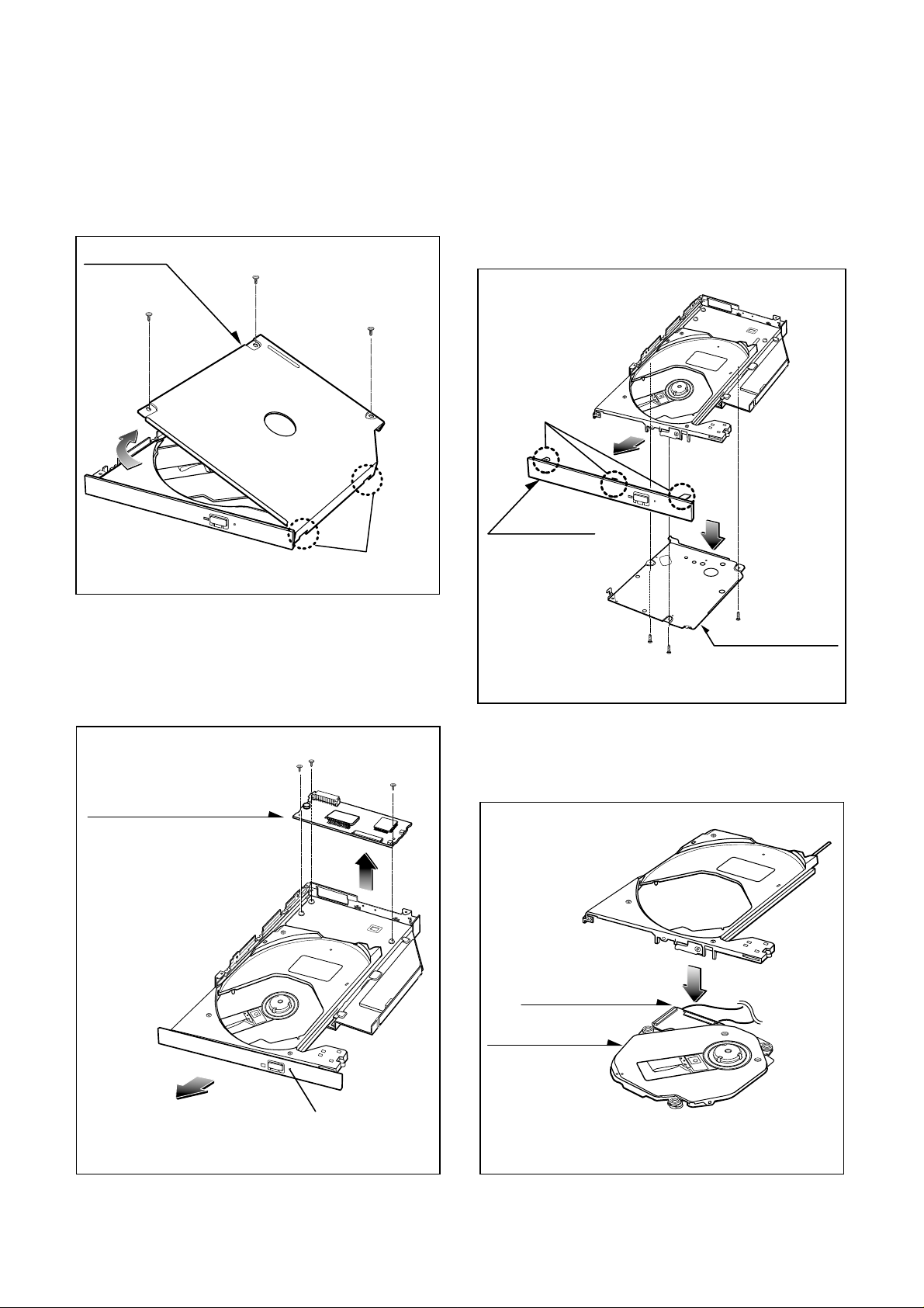
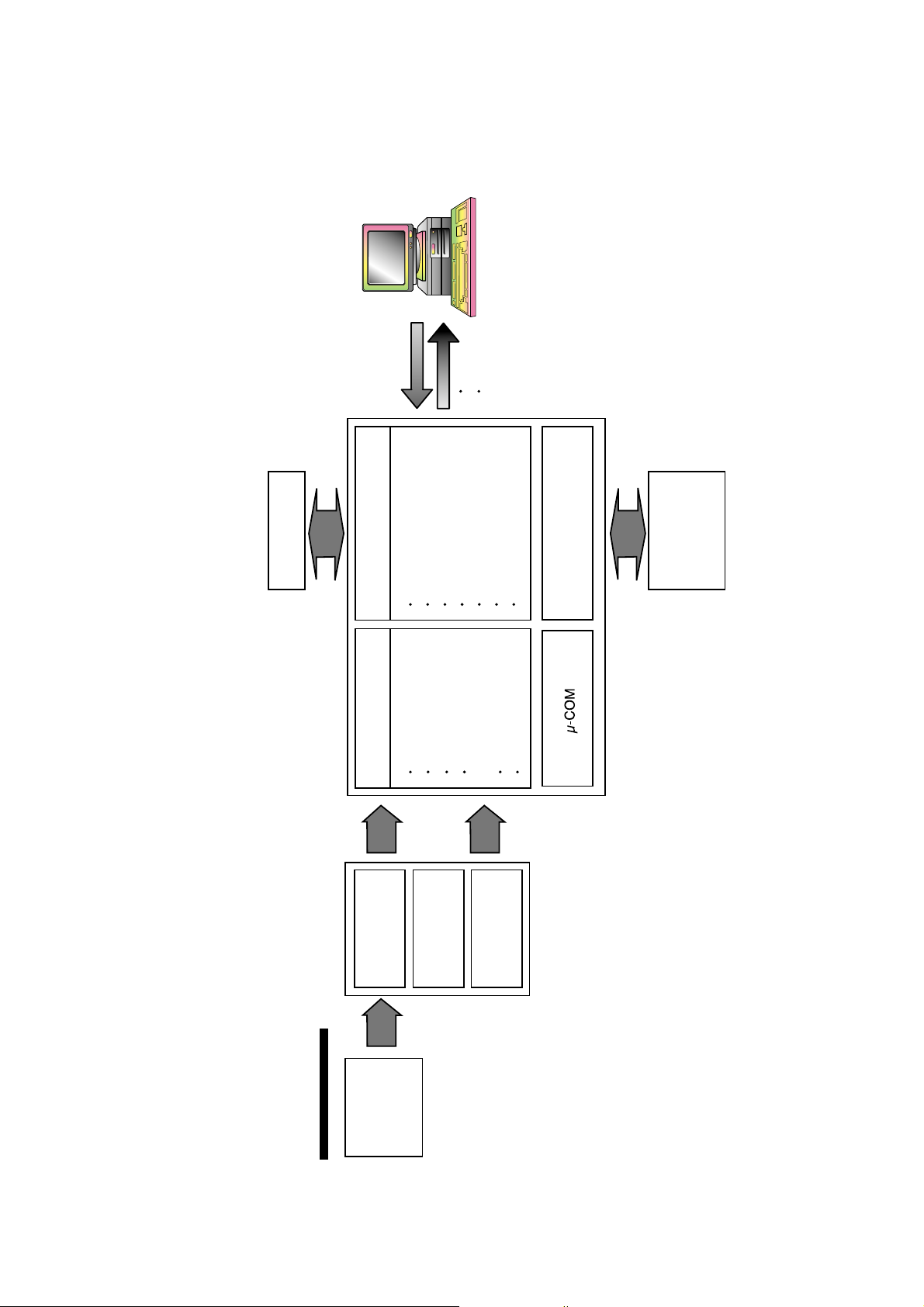
DISASSEMBLY
1. CABINET
A. Release 3 screws (A).
B. Lift up the Cabinet in the direction of arrow (1).
(See Fig.1)
2. MAIN CIRCUIT BOARD
A. Insert and press a rod in the Emergency Eject Hole and
then the CD Tray will open in the direction of arrow (2).
B. Release 3 screws (B).
C. Remove the Main Circuit Board.
3. FRONT PANEL
A. Remove the Front Panel.(The Front Panel is a snap on
type.)
B. At this time, be careful not to damage the 3 hooks (a) of
the it. (See fig.3)
C. Release 3 screws (C) and remove the Cover Bottom (3).
4. BASE PICK-UP
A. Remove the FPC Cable. At this time, the FPC connector
must be pulled in the direction of Front carefully.
B. Remove the Base Pick-up (4).
(1)
(A)
(A)
(A)
CABINET
2 HOOKS
HOOKS (a)
FRONT PANEL
COVER BOTTOM
BASE PICK-UP
FPC CONNECTOR
MAIN CIRCUIT BOARD
EMERGENCY EJECT HOLE
Fig.1
Fig.3
Fig.2
Fig.4
(2)
(3)
(C)
(C)
(C)
(2)
(B)(B)
(B)
(4)
Page 8
8
PBM00(MAIN C.B.A)˚
ABCD
1
2
3
4
5
450
450
450
001
012
011
013
451
451
451
450
450
005
004
003
A02
A00
A01
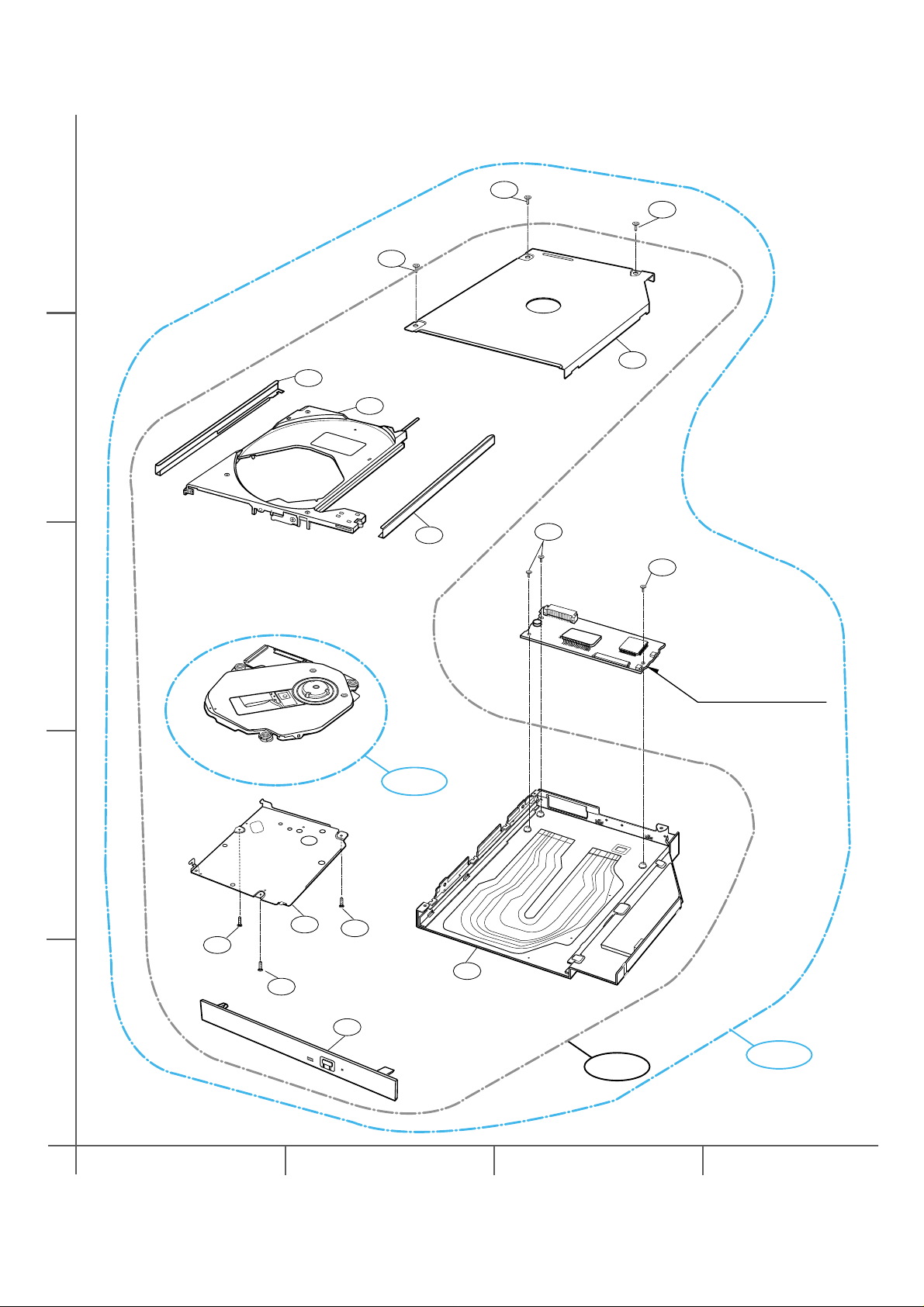
EXPLODED VIEW
Page 9

ATIP Absolute Time in Pre-groove. With an additional modulation of the “Wobble”, the “Groove” contains a time
code information.
Wobble The pre-groove in the Disc is not a perfect spiral but is wobbled.
With : – A typical amplitude of 30 nm
– A spatial peried of 54~64 µm
CW Continuous Wave. The laser light output is at a constant level.
DOW Direct Over-Write. The action in which new information is recored over previously recorded information in
CD-RW disc.
Overwrite
The action in which new information is recorded over previously recorded information.
(Pre-)Groove
The guidance track in which clocking and time code information is stored by means of an FM
modulated wobble.
Land Land is characterized in the following way:
When radial signals are concerned,land is defined as the area between the grooves.
When HF signal are concerned,land is defined as the area between the marks(pits) in tangential
direction.
Hybrid Disc A Multisession disc of which the first Session is mastered. On a hybrid disc, recorded and
mastered information may co-exist.
Mastered Information,stored as pits on the disc during the manufacturing process of the disc.
Information (when making the master)
OPC Optimum Power Control. Procedure is determined optimum recording power according to CD-
R/RW Media in recording start step.
ROPC Running OPC. The purpose is to continuously adjust the writing power to the optimum power
that is required.
When the optimum power may change because of changed conditions of disc and change in
operating temperature.
Jitter The 16 value of the time variation between leading and trailing edges of a specific (I3 … I11) pit
or land as measured by Time Interval Analysis.
Deviation The difference between a fixed value of Pit length and Land length.
TOC Table Of Contents : in the Lead-in Area the subcode Q-channel contains information about the
Tracks on the disc.
Packet A method of writing data on a CD in small increments.
Writing Two kinds of packets can be written : Fixed-length and Variable-length.
Write The shape of the HF write signal used to modulate the power of the laser.
Strategy The Write Strategy must be used for recordings necessary for disc measurements.
Information Wobble, ATIP, Disc Identification, Write Power, Speed Range OPC Parameters, etc are
Area recorded in the Information area of CD-RW Disc
Finalization The action in which (partially) unrecorded or logically erased tracks are finished and the Lead-in
and/or Lead-out areas are recorded or overwritten with the appropriate TOC subcode.
Logical Erase
A method to remove information from a disc area by overwriting it with an EFM signal containing
mode 0 subcode
A logically erased area is equivalent to an unrecorded
Physical Erase
The action in which previously recorded information is erased by overwriting with a CW laser
output.
After a Physical Erase action, the erased area on the CD-RW disc is in the unrecorded state
again.
Session
An area on the disc consisting of a Lead-in area, a Program area, a lead-out area.
Multi session
A session that contains or can contain more than one session composed Lead-in and Lead-out
GLOSSARY
11
Page 10
The differences of CD-R/CD-RW discs and General CD-ROM
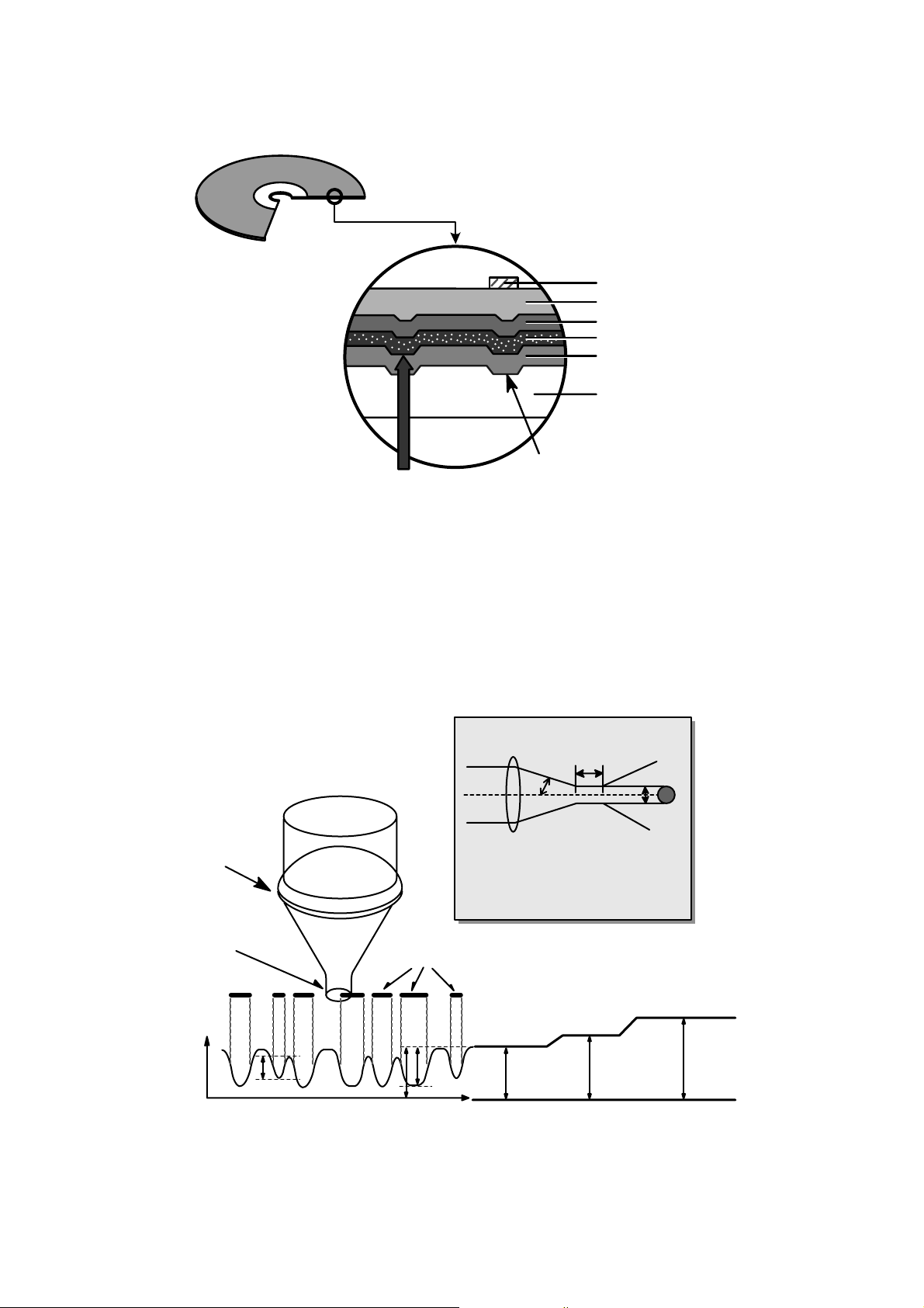
1.Recording Layer
Recordable CD has a wobbled pre-groove on the surface of disc for laser beam to follow track.
2.Disc Specification
Read-only Disc
CD-R and CD-RW Disc
3~1 1T
1.6um
0.4~0.5 um
(Pit)Groove
Land
Track pitch(p)
Radial Direction
Iw
A
O
a
a
Groove
Land
Radial Error Signal
The Groove wobble
Average center
Actual center
CD-ROM CD-R CD-RW
Standard Yellow Book Orange Book II Orange Book III
Record Not available Write once Re-writable
I 11/Itop
> 0.6 > 0.6 0.55 > M11> 0.70
(HF Modulation)
Write Laser Power(mW) 10-30 mW 6-25 mW
Read Laser Power(mW) < 0.5 mW < 0.7 mW < 1.0 mW
Jitter < 35 nsec < 35 nsec < 35 nsec
Reflectivity (R
top) 70 % 65 % 15 % ~ 25 %
12
CD-ROM (READ-ONLY DISC)
a=30nm
Page 11
13
3.Disc Materials
1) CD-ROM disc
Laser Beam
Groove
Substrate
(Polycarbonate)
Organic Dye Layer
Reflective Layer
Protective Layer
Label Printing
2) CD-R disc
Pigment Reflective Layer Color
Phtalocyanine Gold/Silver Yellow/White
Cyanine Gold/Silver Dark Green/Bright Green
Azo Gold/Silver Dark Blue
• It is composed of Silver _ colored aluminum plate and Reflective layer.
• Groove (Pit) of aluminum plate make a track.
• Laser wavelength : 780 nm, Laser Power (Read): 0.5mW
• Signal is detected by the
difference of reflective beam
intensity between “pit” and
“Land” on the disc.
• It is so-called WORM (Write Once Read Many) CD.
• It is composed of polycarbonate layer, Organic dye layer, Reflective layer, and Protective
layer.Gold/Silver Reflective layer is used to enhance the reflectivity
• According to the kinds of Organic dye layer, it is divided by Green CD, Gold CD, Blue CD.
• Laser Wavelength : 780 nm, Laser Power (read) : 0.7 mW
• Recording Power : 4x(10~15mW), 8x(14~20mW), 12x(15~30mW), 16x(25~35mW).
• When some part of dye layer is exposed to laser heat, it’s color changs black.Therefore, writing and
reading is enabled by the difference of reflectivity between changed part and unchanged part.
• Polycarbonate layer has Pre_Groove which make a Track.
Laser Beam
Pit
Substrate
(Polycarbonate)
Reflective Layer
Protective Layer
Label Printing
Page 12
14
3) CD-RW Disc
4.
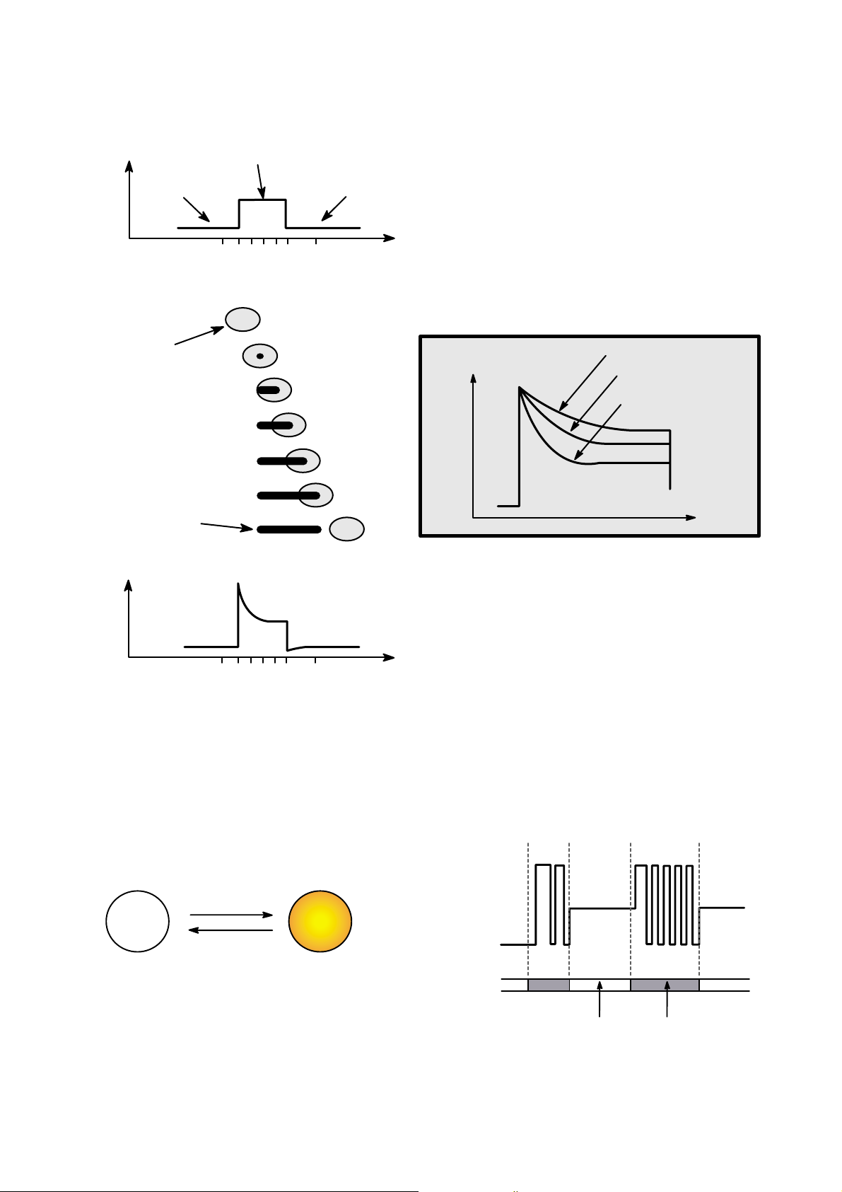
Reading process of Optical Disc
Laser Beam
Groove
Substrate
(Polycarbonate)
Reflective Layer
Dielectric Layer(TL)
Dielectric Layer(UL)
Protective Layer
Label Printing
• It is composed of polycarbonate layer, alloy(silver, arsenic) layer, aluminum reflectivity layer, protective layer.
• An crystalized alloy layer is transformed into noncrystalized by the laser heat. Therefore, writing and reading
is enabled by the difference of reflectivity.
• It is possible to overwrite about 1000 times.
• Laser Wavelength : 780 nm, Laser Power (Read) : 1.0mW
• Recording Power : Erase (4~18mW), Write (6~45mW)
• When disc rewriting, new data is overwritten previously recorded data.
• Polycarbonate layer has a Pre-Groove which make a track.
Lens
H
D
Beam
Spot
Focusing
Lens
Laser Spot
at Constant
Read Intensity
Reflected
Light
Signal
Laser Spot
Position
(Time)
Previously Recorded Marks
Groove Land Mirror
I
3
I
top
I
11
I
G
I
L
I
0
N
umerical aperture:NA=nsinθ,
n: Refractive index
Focus depth : H =
λ
/NA
laser spot diameter : D =
λ
/NA
2
θ
Page 13
15
5.Writing Process of CD-R Disc
a b c d e f g
a
b
c
d
e
f
g
Incident
Laser
Power
(Read)
(Read)
(Write)
Laser Spot
Position
(Time)
a b c d e f g
Laser Spot
Position
(Time)
Laser
Spot
Recorded
Mark
Reflected
Light
Signal
Reflected
Light
Signal
Below "ORP"– Mark Too Short
At Optimum Record Power ("ORP")
Above "ORP" – Mark Too Long
Time
6.Writing process of CD-RW Disc
Write Power
Erase Power
Read Power
Groove
Crystal
Amorphous
Amorphous
Recorded state
(lower reflectivity)
Melting/
quenching
Heating/
gradual cooling
Crystal phase
Erased state
(higher reflectivity)
Page 14
7.Organization of the PCA, PMA and Lead-in Area
1) Layout of CD-ROM disc
16
Center hole Clamping and Label Area Information Area
Lead-in Area
Lead-in Area
Diameter 15 mm
Diameter 46 mm
Diameter 120 mm
Program Area
Read Only Disc
Lead-out Area
Program Area Lead-out Area
Center hole
Clamping and Label Area
Information Area
PCA PMA
Test Area Count Area
Diameter 15 mm
Diameter 45 mm
Diameter 120 mm
Unrecorded Disc
Tsl-00:35:65 Tsl-00:15:05
Tsl-00:13:25
Tsl
99:59:74
00:00:00
in out
Test Area : for performing OPC procedures.
Count Area : to find the usable area immediately in T.A
Tsl : start time of the Lead-in Area, as encoded in ATIP
PMA : Program Memory Area
Disc Center
Disc Center
2) Layout of CD-R/RW disc
Page 15
17
8. Function of PCA and PMA area
1) PCA (Power Calibration Area)
• PCA area is used to determine the correct Laser Power for a disc.
– Method 1 : PCA area is divided by a track.
– Method 2 : The previous Calibration value is referred.
– Method 3 : ROPC is used to determine Laser Power value automatically in data writing.
• CD-R Disc can write maximum 99 Tracks but CD-RW Disc can write unlimited tracks because it has a rewritable
function.
2) PMA (Program Memory Area)
• It has a track information (track No, track Start/End time) of every track before writing completed.
– PMA area has the last written point and the next writable point of a disc.
– In case of CD to CD copy, some writer may not write PMA area.
* When Disc is Finalized,
PMA information is transferred to the Lead_In area so that general Driver can read it.
* Because PCA and PMA area exist before Lead-In area, General CD Player or CD-ROM Drive can’t read
these areas.
9. OPC and ROPC
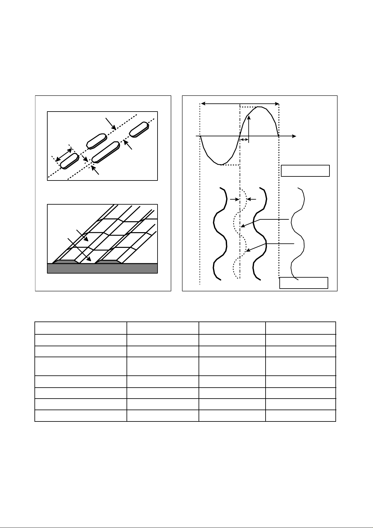
1) OPC (Optimum Power Control)
• This is the first step of writing process, because CD writer has its own laser power value and media have different
writing characteristics,
– This is determined by the Writing characteristic, speed, temperature, and humidity.
– Laser wavelength is determined by the environmental temperature (775~795nm) and Optical Laser Power is
determined by the test and retry.
• Asymmetry and optimum writing Power
– EFM signal Asymmetry is determined by the writing power.
Therefore, Optical Power which has the same value to the preset power value can be estimated by measuring
HF signal Asymmetry on the PCA area.
• Measurement of Asymmetry
* Parameter setting (Beta) : Using AC coupled HF signal before equalization
Beta = (A1+A2)/(A1-A2)
Time
P << Po
Time
P = Po
HF Signal
A1
0
A2
Time
P >> Po
Page 16
2) ROPC (Running Optimum Power Control)
• Variable primary factor of Optimum Power
– Change of Power sensitivity on the Disc. (limited to 0.05 *Po)
– Wavelength shift of the laser diode due to the operating temperature change.
– Change of the Spot aberration due to the Disc skew,
Substrate thickness, Defocus.
– Change of Disc or Optics conditions due to the long term OPC
==> It is necessary to adjust continuously to obtain the Optimum Power.
• Principle of Running OPC
– To meet the factors mentioned above,
a horizontal _ direction movement of a curve is uesd.
– Beta = f(B-level) = constant on the Recorded Disc
– Procedure of ROPC
a. Reference B-level is determined during OPC Procedure.
b. During Recording, B-level value is controlled to have a close
Reference B-level value.
c. Normalization of B-level is used to eliminate the effect of reflectivity fluctuation.
==> The reflected B-level value is normalized by the disc reflectivity itself.
18
CD-R/RW Media
Write Strategy
Determination
PCA Test Area
Program Area
PMA Area
Lead-In Area
Lead-out Area
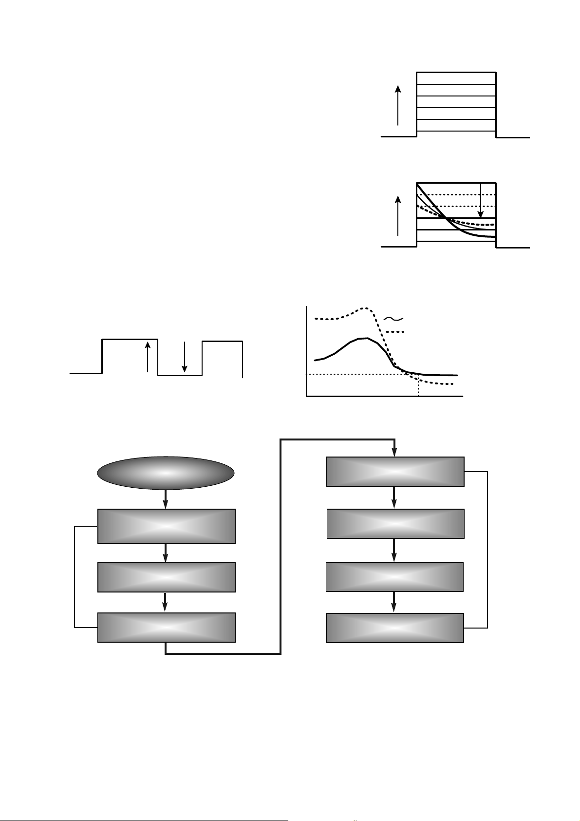
OPC
PCA Count Area
ROPC
* Recording Capacity of CD-R/RW (74Minute Recording media)
• (2048 Byte/Sector) X (75 Sector/Second) X (60 Second/Minute) X 74 Minute
= 681,984,000 Bytes = 682 Mbytes
• But the actual recording capacity is about 650 Mbytes. (according to the ISO 9660 standard, approximately
30 Mbytes are used to make directory structure and volume names.)
Incident recording pulse
Reflected recording pulse
Sampled timing B
11T
Sample B-level (Write Power)
Level B
Sampled at timing B
Pwo decided by OPC
Recording Power
Level B with Pwo
normalized to recording power
Sample Disc Reflectivity
(Read power)
10. Writing Process of DISC
Page 17
19
DESCRIPTION OF DATA PROCESSING
1.Data Processing Flow
Command
Data
Status
RF EQ & AGC
SERVO
DSP
Decoder & CSS
RF data slice EFM demodulator
CiRC error correction
Audio DAC
C3 decoder
Buffer/Memory controller
CSS controller
Atapi interface control
Data PLL
Servo ADC
Focus/tracking
control output
Sled control output
CAV Spindle control
P-up
Unit
IC101
(AN22107A)
RF AMP
CD
DVD
IC201
(MN103S63G)
TE/CSO GEN
FE GEN
FLASH ROM
DRAM
IC602
IC601 DRAM
Page 18

MN103S63G
HOST DVD
PLAYER
(EMPEG2 B/D)
Scrambled MPEG Data
Change the "KEY"
KEY Management Control
2. Copy Protection and Regional Code Management Block
Block Diagram
Brief Process
1. Regional Code for DVD Disc
– DVD-ROM drive transfers the regional code of the control data to host by the command of host, the DVD
player of host reads the regional code, and plays title in the case of allowed regional code only.
2. Management of DVD Disc for the scrambled of data
(1) DVD-ROM and DVD player of host generate the “KEY 1” respectively, transfer to opposite part, the
“KEY 2” is received, recognizes the data transfer or not with this value, and generates the bus key
encoded the data.
(2) Encoded “Disc Key” and “Title Key” host is transfer with the bus Key.
(3) DVD player of host reads the key value, and uses the value to restore the scrambled data.
* Refer to the next page for the details.
20
Page 19
21
3. About Prevention the DVD-ROM from to be copy
A data is able to encode and record in the disc, if a copyright holder wants to prevent the disc from copying.
In case of a disc enhanced movie of 3 titles......
DISC KEY (2048 Bytes) is used to encode the whole contents in the disc and TITLE
KEY (5 Bytes) is used to encode the title respectively.
So, the data is encoded and stored in a disc through the unknown algorithms
with a disc key and title key. (At this time, the disc key and title key are stored
in a disc.)
…As above, the disc is able to copy when the disc key and title key are
opened.
Then, ROM-DRIVE encodes the disc key and title key and transfers to MPEG2 board.
If you want to play the disc prevented from the copy......
First of all, ROM-DRIVE and MPEG-2 decoder identify with each other through the procedure as
described below.
1. Drive and host gives and takes the ID of 2bit. This ID is AGID (Authentication Grant ID).
The various decoder boards are attached to the host, in these, AGID sets the MPEG-2 decoder and drive.
2. After the AGID is set, MPEG-2 decoder generates the challenge key (10 Byte) and transfers to drive. The
board and drive generate key 1 (5Byte) with the challenge key respectively. (Of course, the Algorithm
generating the key 1 is not known.)
3. Compare with the generated key 1, if it corresponds each other, the first step of authentication is
completed. This is a course to identify the MPEG-2 decoder with a drive.
4. The second step of authentication is a course to identify a drive with the MPEG-2 decoder.
The dirve generates a challenge key and transfers it to the MPEG-2 decoder. The dirve and MPEG-2
decoder generate the key 2 (5Byte) with the challenge key, compare with each other, and if it corresponds
and the secondary step of authentication is completed.
5. As above, the identification is completed.
6. The dirve and MPEG-2 decoder generate the Bus key with the key 1 and key 2 and own it.
7. Dirve encodes the disc key and title key with this Bus key and transfers to the MPEG-2 decoder.
8. The MPEG-2 decoder reads the encoded disc key and title key with the Bus key only.
9. MPEG-2 board lets data read from the drive to decode with the read disc key and title key and makes into
the video signal by decoding.
ROM-DRIVE
AGID
HOST
MPEG-2
DECODER
Challenge key
encoded disc key, title key
Page 20

22
4.About the DVD-ROM Regional Code
DISC ROM - DRIVE MPEG-2 DECODER VGA CARD
MONITOR
1
CAN
U.S.A
MIX
CUB
BHS
PRI. VIR
1
BMG
GRL
2
2
ZAF
ISO
SWZ
FIN
POI
FST
LTU
BIR
UKR
TUR
FGY
JRN
TKM
AFG
PAK
CHN
MMR
MNG
RUS
KOR
JPN
HKG
MAC
TWN
PHL
6
3
2
1
5
5
4
1
MDI
MNP
GUM
PLW
PNG
NZL
AUS
4
The disc has
the regional
code of 8 bit.
Example)
The disc
manufactured
in the U.S.A,
has the
number one.
Transfer to
MPEG-2
decoder
reading the
regional code.
If the board is setting to the regional
code 1 for the U.S.A. ...
Check the received regional code to
number 1, all or not, transfer the
data to VGA card in accordance with
only a case among the three case.
Regional code
Receiving
data from the
MPEG-2
decoder and
output
through the
monitor
Page 21

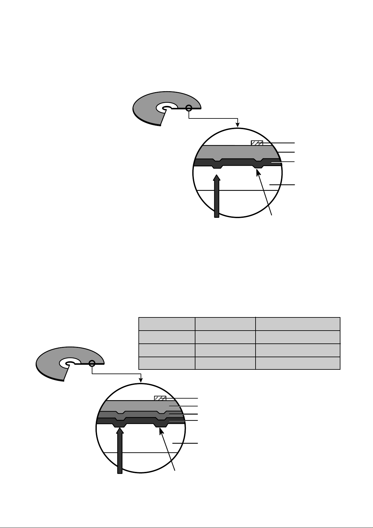
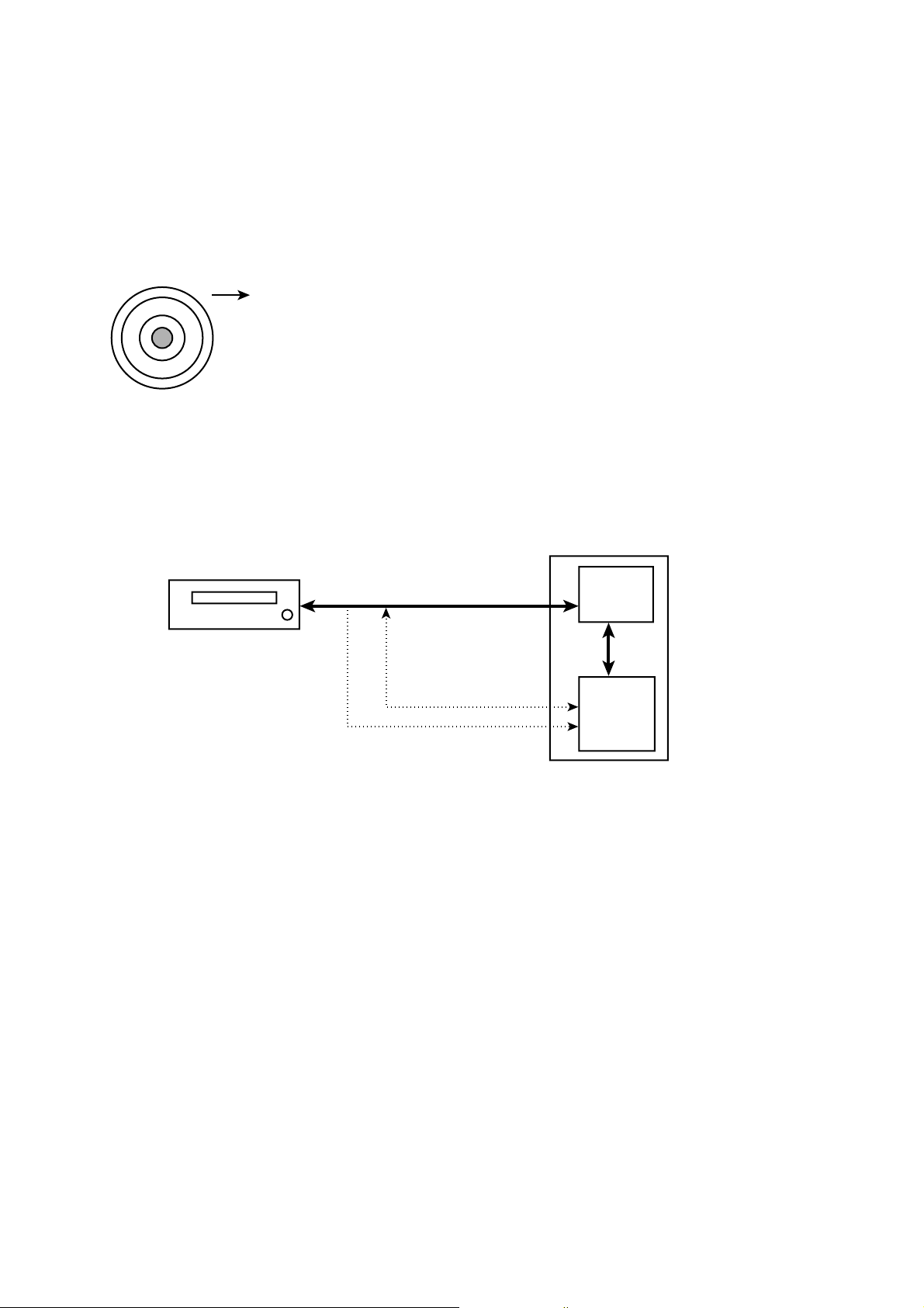
INTERNAL STRUCTURE OF THE PICK-UP
1.Inner Circuit of the PICK-UP(HOP-6061T)
23
operating
Page 22

2.Signal detection of the P/U
1) Focus Error Signal ==> (A+C)-(B+D)
This signal is generated in RF IC (IC101 : AN22107A) and controls the pick-up’s up and down to focus on
Disc.
2) Tracking Error Signal (DPP Method) ==> {(A+D)-(B+C)}- k x {(F+H)-(E+G)}
This signal is generated in RF IC (IC101 : AN22107A) and controls the pick-up’s left and right shift to find
to track on Disc.
3) RF Signal ==> (A+B+C+D)
This signal is converted to DATA signal in DSP IC (IC201 : MN103S63G).
24
Pick-Up module
Photo Diode
Tracking
Focusing
Infrared Iaser
k[(F+H) - (E+G)]
(A+D) - (B+C)
(A+D) - (B+C) - k[(F+H) - (E+G)]
Offset
TE
Tp
Sub2
Main
Tp/2
Sub1
T rac k Center
F,E
D,C
A,B
H,G
Page 23

MAJOR IC INTERNAL BLOCK DIAGRAM AND PIN DESCRIPTION
IC101 (AN22107A) : RF Signal Processor for Drive
Block Diagram
25
Comp. BPF
S/H AGC
CLKO
SERVO
Focus error
SSD, ASD, DASD, NE
Tracking error
DPP, PP
DPD
VGA
&
offset
Comparator
TOK
ADO-MONO-2
STANBY
CD APC
DVD
LPC
MPX
SERVO
DAC
Read APC DAC
Write APC DAC
MPX
LOGIC
Serial-I.F
CLKO
Input-selector & S/H Matrix circuit
AS, TC, LE
CLK
gen.
WOBBLE
Band-gap
Ref-current
RECD
AGC, EQ
DET
OPC/RFENV
RFENV
ROPC
BDO, OFTR
MIRROR
AGC
EQ
CLKO
RECD
RRF, WRF signal
RFSUM
75
VCC1
1
TCFLT0
2
TCFLTIN
3
SDOUT
4
SDIN
5
GND4
6
ADO
7
MONI08MONI19MONI2
10
VHALF
11
VR0612LPC113LPC0
14
EDRV
15
FPDMN
16
FPDMP
17
GND3
18
RDRVN219RDRVN1
20
RDRV
21
RREFDET
22
WDRVN223WDRVN1
24
WDRV
25
WREFDET
76
WBL
50
(NC2)
49
VCC5
48
BMC
47
PKC
46
RFENV
45
CDEFECT
44
GND2
41
OFTR
40
BDO
39
VDD
38
(NC1)
37
SCK
36
SEN
35
STDIO
34
TOK
33
XWTGT
32
ADCLR
31
ADCK
30
VSS
29
XSTANBY
28
/VFOSHORT
RAPC
27
WAPC
26
VCC3
43
ROPCSH2
/DTRD
42
ROPCSH1
/IDGT
77
SCFCLK
78
(NC4)
79
WSH
80
SSH
81
GND1
82
AIN
83
BIN
84
CIN
85
DIN
86
EIN
87
GIN
88
GIN
89
HIN
90
HDVREF
91
F01
92
F02
93
TR1
94
TR2
95
TR3
96
TR4
97
TR5
98
TR6
99
VCC4
100
TEZX
74
WHPF273WHPF172WAGC171WAGC270WAGC369CWBL68(NC3)67JLINE66CRECD65RSCL64VREF63RF OUT62RFDIFO61VCC260WRFIN59DCRF58TESTSG57RF INN56RF INP55AGCG54AGCO53DCFLT52DFLTON51DFLTOP
Page 24

26
• Pin Descriptions
The following table shows a list of I/O pin specifications.
* The following codes are used in the table.
I : Input pin
O : Output pin
I/O : I/O pin
PS : Power supply/Ground pin
MSC: Resistor/Capacitor connection pin or others
No. Name I/O Funtion
1 TCFLTO O Tracking detection filter
2 TCFLTIN I Track detection filter
3 SDOUT O Tracking error signal output
4 SDIN I Comparetor input for anti shock detection
5 GND4 PS GND for SERVO I/F (3.3V)
6 AD0 O servo error signal output for A/D
7 MONI0 O Analog signal monitor output 0
8 MONI1 O Analog signal monitor output 1
9 MONI2 O Analog signal monitor output 2
10 VHALF O Reference voltage output (1.65V)
11 VR06 O Reference voltage output (0.6V)
12 LPC1 I Laser pin input (DVD head)
13 LPC0 O Laser drive output (DVD head)
14 EDRV O Extra power DAC output (DVD head)
15 FPDMN I Front monitor signal reference voltage
16 FPDMP I Front monitor signal input
17 GND3 PS GND for APC(5V)
18 RDRVN2 I APC integrator(READ) negative input2
19 RDRVN1 I APC integrator(READ) negative input1
20 RDRV O Laser drive output(READ)
21 RREFDET I DAC input for READ
22 WDRVN2 I APC integrator(WRITE) negative input2
23 WDRVN1 I APC integrator(WRITE) negative input1
24 WDRV O Laser drive output (WRITE)
25 WREFDET I DAC input for WRITE
26 VCC3 PS Power supply for APC(5V)
27 WAPC I APC write sample&hold timing input
28 RAPC I APC read smaple&hold timing input
/VFOSHO
RT
29 XSTANBY I STANBY setting
30 VSS PS GND for LOGIC(5V)
31 ACK I signal selecter clock for A/D
32 ACLR I signal selecter reset for A/D
33 XWTGT I Write gate signal input
34 TOK O Comparetor output for anti-shock
35 STDIO I/O Serial data Input/Output
36 SEN I Serial enable input
37 SCK I Serial clock input
38 NCI - Non connection
39 VDD PS Power supply LOGIC(5V)
40 BDO O BDO output
41 OFTR O OFTR&TC output
42 ROPCSH1 I ROPC1 sample&hold timing input
/IDGT
43 ROPCSH2 I ROPC2 sample&hold timing input
/DTRD
44 GND2 PS GND for RF(5V)
45 CDEFECT - DEFECT envelope detection filter
46 RFENV O RF envelope output
47 PKC MSC Peak envelope detection filter
48 BMC MSC Bottom envelope detection filter
No. Name I/O Funtion
49 VCC5 PS Power supply CMOS I/F (3.3V)
50 NC2 - Non connection
51 DFLTOP O Filter amplifier positive output
52 DFLTON O Filter amplifier inverted output
53 DCFLT MSC DC cut filter for Filter output
54 AGCO I RF AGC amplifier level control
55 AGCG I RF AGC amplifier gain control
56 RFINP I RF signal positive input
57 RFINN I RF signal inverted input
58 TESTSG I I TEST signal input
59 DCRF MSC DC cut filter for RF amplifier
60 WRFIN I Write RF signal input
61 VCC2 PS Power supply RF (5V)
62 RFDIFO O Radial differential output
63 RFOUT O RF signal output
64 VREF O Reference voltage output(2.2V)
65 RSCL I S Line current setting
66 CRECD I DC cut filter for RECD
67 JLINE I J Line current setting
68 NC2 - Non connection
69 CWBL MSC DC cut filter for wobble
70 WAGC3 MSC WBL AGC3 amplifier gain control
71 WAGC2 MSC WBL AGC3 amplifier gain control
72 WAGC1 MSC WBL AGC2 amplifier gain control
73 WHPF1 MSC WBL HPF1 capacitance connection
74 WHPF2 MSC WBL HPF2 capacitance connection
75 VCC1 PS Power supply SERVO/WBL(5V)
76 WBL O Wobble signal output
77 SCFCLK I Clock input for Wobble BPF
78 NC3 - Non connection
79 WSH I WBL sample hold timing input
80 SSH I Servo Sample hold timing input
81 GND1 PS GND for SERVO/WBL(5V)
82 AIN I AIN input
83 BIN I BIN input
84 CIN I CIN input
85 DIN I DIN input
86 EIN I EIN input
87 FIN I FIN input
88 GIN I GIN input
89 HIN I HIN input
90 HDVREF I Detector signal Reference voltage
91 FO1 I FO1 input
92 FO2 I FO2 input
93 TR1 I TR1 input
94 TR2 I TR2 input
95 TR3 I TR3 input
96 TR4 I TR4 input
97 TR5 I TR5 input
98 TR6 I TR6 input
99 VCC4 PS Power supply SERVO I/F(3.3V)
100 TEZX O TEOUT in radial seeking
Page 25

IC201(MN103S63G) : ATAPI Interface, Write and DSP Signal Processor
Block Diagram
27
*1. Shaded blocks
: Work as system controller functions.
: New blocks for MN103S63G (MN103SEM0T63)
*2. The MN103SEM0T63 uses a 256-Kbyte SRAM as an instruction memory,
16-Kbyte data memory (8-Kbyte f/w and 8-Kbyte microcode), and 2-Mbit DRAM.
32-bit
CPU core
BCU
DRAMC
DMA
1-Mbit
DRAM
OnChip
Debug
Data memory
(6-Kbyte f/w)
(4-Kbyte microcode)
Instruction
memory
(128 Kbytes)
CGEN
MODE
WDT
16-bit
timerx6 f/w
timerx2 microcode
SYSTEM
I/F
INTC
General-
purpose
I/O
Serial
interface
HOST I/F
MPEG I/F
ECC
DMA I/F
ATAPI
General-pu rp ose I/O bus
SERVO
IO
(Core1 IO)
SERVO
core
(Core2)
RAM
CIRC
DVD-
ROM
Formatter
CD-
PRE
High-speed I/O bus
ANALOG
ATIP
BUEP
CDENC
Write
Strategy
DRAM I/F
Page 26

• Pin Assignment
28
0
FDT0
FDT8
FDT1
FDT9
FDT2
FDT10
FDT3
FDT11
FDT4
FDT12
FDT5
FDT13
FDT6
FDT14
FDT7
FDT15
FADR16
P1
P0
_VSS
_VDD3
VDDH
VSS
MASTER
NRESET
HDD7
HDD8
HDD6
HDD9
VSS
VDD3
HDD5
HDD10
HDD4
HDD11
HDD3
HDD12
HDD2
HDD13
VDD3
VDD15
VSS
HDD1
HDD14
HDD0
HDD15
NDASP
NCS3FX
NCS1FX
DA2
DA0
NPDIAG
DA1
NIOCS16
INTRQ
NDMACK
VSS
VDD3
IORDY
NIORD
NIOWR
DMARQ
0
Ve
r. 0.99
NC
241
240
239
238
237
236
235
234
233
232
231
230
229
228
227
226
225
224
223
NC
NC
222
221
220
219
218
217
216
215
214
213
212
211
210
209
208
207
206
205
204
203
202
201
200
199
198
197
196
195
194
193
192
191
190
189
188
187
186
185
184
183
182
NC
241
256
255
254
253
252
251
250
249
248
247
246
245
244
243
242
241
240
239
238
237
236
235
234
233
232
231
230
229
228
227
226
225
224
223
222
221
220
219
218
217
216
215
214
213
212
211
210
209
208
207
206
205
204
203
202
201
200
199
198
197
196
195
194
193
256
NOE 1 1 192 181 NTRYCL
NCE 2 2 191 180 NE JECT
FADR 0 3 3 190 17 9 DASPST
FADR 1 4
4
189 178
MSTPOL
FADR 2 5 5 188 177 P12
FADR 3 6 6 187 176 P11
FADR 4 7 7 186 175 P10
VDD3 8 8 185 174 P9
VDD15 9 9 184 173 TX
VSS 10 10 183 172 VDD3
FADR 5 11 11 182 171 OSCI
FAD
R6 12 12
181
170 OSCO
FADR 7
13 13
180 169
VSS
FADR 8 14 14 179 168 DA
C1
P7
15 15
178
167 DAC0
P8 16 16 177 166 AVSSA
P17 17 17 176 165 AD2
NWE 18 18 175 164 AD1
FADR 9 19 19 174 163 AD0
FADR10 20 20 173 162 ADIN
_VDD3 NC 21 172 161 AVDDA
VSS 21 22 171 160 JITOUT
FADR11 22 23 170 159 AVDDB
FADR12 23 24 169 158 DSLF1
FADR13 24 25 168 157 DSLF2
FADR14
25 26
167 15
6 VREFH
MMOD 26 27 166 155 RVI
FADR15 27 28 165 154 VHALF
DRAMVDD15 28 29 164 153 NARF
VOUT 29 30 163 152 ARF
DRAMVDD33 30 31 162 151 AVSSB
DRAMVSS 31
32
161 150
PLFLT1
_VSS NC 33 160 149 PLFLT2
TxD 32 34 159 148 AVSSC
SCLO
CK 33 35
158 147
RFDIF
NRST 34 36 157 146 CSLFLT
SDATA 35 37 156 145 WBLIN
RxD 36 38 155 144 AVDDC
P2 37 39 154 143 TRCRS
P3 38 40 153 142 VCOF
P4 39 41 152 141 AVDDD
P5 40 42 151 140 LOUT
P6 41 43 150 139 ROUT
_VSS NC 44 149 138 AVSSD
DRV4 42 45 148 NC _AVSSD1
DRV5 43 46 147 137 CPOP5
DRV6 44 47 146 136 AVDDD1
DRV7 45 48 145 135 CPOP4
VDD3 46 49 144 134 AVDDWBLC
MDQ0 47 50 143 133 JLINE
MDQ15 48 51 142 132 VFOSHORT
MDQ1 49 52 141 131 TSTSG
MDQ14 50
53
140 130
DRV11
MDQ2 51 54 139 129 DRV10
MDQ13 52 55 138 128 DRV9
MDQ3 53 56 137 127 DRV8
MDQ12 54 57 136 126 ADST1
MDQ4 55 58 135 125 ADST0
VDD3 56 59 134 124 VSS
VSS 57 60 133 123 VDD3
MDQ11 58 61 132 122 SH6
MDQ5 59 62 131 121 SH5
MDQ10 60 63 130 120 SH4
NCC64 129 119 SH3
256
6566676869707172737475767778798081828384858687888990919293949596979899
100
101
102
103
104
105
106
107
108
109
110
111
112
113
114
115
116
117
118
119
120
121
122
123
124
125
126
127
128
256
241
NC
616263
64NC656667686970717273747576777879808182838485
86
NC
NC
87888990919293949596979899
100
101
102
103
104
105
106
107
108
109
110
111
112
113
114
115
116
117
118
NC
NC
241
0
MDQ6
MDQ9
MDQ7
VDD3
_VDD15
VSS
MDQ8
MDQML
MNWE
MDQMU
MNCAS
MCLKI
VSS
MCLK
VDD3
MNRAS
MCKE
MBA0
MA11
MBA1
MA9
MA10
MA8
MA0
MA7
VSS
VDD15
_DRAMVDD15
_DRAMVSS
VDD3
MA1
MA6
MA2
MA5
MA3
MA4
WGATE
NWGATE
HFSW
SH7
VSS
LDCNT2
VDD3
LDCNT1
VSS
DRV0
DRV1
DRV2
DRV3
FG
WBLI
BDO
OFTR
DRV12
DRV13
DRV14
SCFCK
VSS
VDD3
SH1
SH2
0
0
MN103S63GKD
241-pin version
Page 27

29
• Pin Functions
256 241 Pin name
System controller
external connection
I/O Destination Description
1 1 T2 NOE NRD(I) O Flash Read signal output to flash
2 2 U3 NCE NCS(I) O Flash Chip select signal output to flash
3 3 T1 FADR0 CPUADR0(I) O Flash Address output to flash
4 4 R2 FADR1 CPUADR1(I) O Flash Address output to flash
5 5 T4 FADR2 CPUADR2(I) O Flash Address output to flash
6 6 R1 FADR3 CPUADR3(I) O Flash Address output to flash
7 7 P5 FADR4 CPUADR4(I) O Flash Address output to flash
8 8 - V
DD3
Power
supply
-
VDD (3.3 V)
9 9 - V
DD15
Power
supply
-
V
DD
(1.5 V)
10 10 - VSS
GND
-
VSS
11 11 M4 FADR5 CPUADR5(I) O Flash Address output to flash
12 12 P1 FADR6 CPUADR6(I) O Flash Address output to flash
13 13 T3 FADR7 CPUADR7(I)
Flash Address output to flash
14 14 N2 FADR8 CPUADR8(I) O Flash Address output to flash
15 15 P4 P7/FADR17 NINT0(O) I/O Flash Address output to general-purpose port/flash
16 16 N1 P8/FADR18 CPUADR17(I) I/O Flash Address output to general-purpose port/flash
17 17 N4 P17/FADR19
I/O Flash Address output to general-purpose port/flash
18 18 P3 NWE NWR(I) O Flash Write signal output to flash
19 19 K5 FADR9 CPUADR9(I) O Flash Address output to flash
20 20 M2 FADR10 CPUADR10(I) O Flash Address output to flash
21 NC NC _V
DD3
Power
supply
-
V
DD
(3.3V)
22 21 - VSS
GND
-
VSS
23 22 L4 FADR11 CPUADR11(I) O Flash Address output to flash
24 23 M3 FADR12 CPUADR12(I) O Flash Address output to flash
25 24 M1 FADR13 CPUADR13(I) O Flash Address output to flash
26 25 K4 FADR14 CPUADR14(I) O Flash Address output to flash
27 26 L3 MMOD
I
-
Test mode selection signal
28 27 K3 FADR15 CPUADR15(I) O Flash Address output to flash
29 28 L1 DRAMV
DD15
Power
supply
-
DRAM power supply (1.5 V)
30 29 L2 VOUT
Regulator output (1.5 V)
31 30 K1 DRAMV
DD33
Power
supply
-
DRAM Power supply(3.3V)
32 31 J1 DRAMVSS
GND
-
VSS fo r DRAM use
33 NC NC _VSS
GND
-
VSS
34 32 J4
TxD/EXTRG0/M
DAT A
I/O Debug Trigger pin fo r serial transmission/Dwire use
Page 28

30
256 241 Pin name
System controller
external connection
I/O Destination Description
35 33 J2 SCLOCK I/O Debug Clock pin for Dwire use
36 34 J3 NRST I
-
Reset input
37 35 H1 SDATA I/O Debug Data pin for Dwire use
38 36 G3
RxD/EXTRG1/M
CLOCK I/O Debug Trigger pin for serial reception/Dwire use
39 37 H2 P2/EXINT0 NINT1(O) I/O Misc General-purpose port/External pin interrupt
40 38 J5 P3/EXINT1 NINT2(O) I/O Misc General-purpose port/E xternal pin interrupt
41 39 H3 P4/EXCNT0 WAITODC(O) I/O Misc General-purpose port/External pin count
42 40 G5 P5/EXCNT1 CLKOUT(O) I/O Misc General-purpose port/External pin count
43 41 F1 P6/NSPCCS NMRST(O) I/O Misc CS for general-purpose port/SPC use
44 NC NC _V
SS
GND
-
V
SS
45 42 F3 DRV4 I/O Misc General-purpose port
46 43 G1 DRV5 I/O Misc General-purpose port
47 44 E3 DRV6 I/O Misc General-purpose port
48 45 G2 DRV 7 I/O Misc General-purpose port
49 46 - V
DD3
Power
supply
-
V
DD
(3.3 V)
50 47 H4 MDQ0 I/O DRAM SDRAM data
51 48 E6 MDQ15 I/O DRAM SDRAM data
52 49 G4 MDQ1 I/O DRAM SDRAM data
53 50 D3 MDQ14 I/O DRAM SDRAM data
54 51 F2 MDQ2 I/O DRAM SDRAM data
55 52 C3 MDQ13 I/O DRAM SDRAM data
56 53 E1 MDQ3 I/O DRAM SDRAM data
57 54 C4 MDQ12 I/O DRAM SDRAM data
58 55 E2 MDQ4 I/O DRAM SDRAM data
59 56 - V
DD3
Power
supply
-
V
DD
(3.3 V)
60 57 - V
SS
GND
-
VSS
61 58 C2 MDQ11 I/O DRAM SDRAM data
62 59 D1 MDQ5 I/O DRAM SDRAM data
63 60 D2 MDQ10 I/O DRAM SDRAM data
64 NC NC 0
65 NC NC 0
66 61 B3 MDQ6 I/O DRAM SDRAM data
67 62 A3 MDQ9 I/O DRAM SDRAM data
68 63 B4 MDQ7 I/O DRAM SDRAM data
69 64 - V
DD3
Power
supply
-
V
DD
(3.3 V)
70 NC NC _V
DD15
Power
supply
-
V
DD
(1.5 V)
Page 29

31
256 241 Pin name
System controller
external connection
I/O Destination
Description
71 65 - VSS GND
-
VSS
72 66 C5 MDQ8 I/O DRAM SDRAM data
73 67 B5 MDQML O DRAM SDRAM data
74 68 E7 MNWE O DRAM SDRAM control
75 69 A4 MDQMU O DRAM SDRAM data
76 70 C6 MNCAS O DRAM SDRAM control
77 71 A5 MCLKI I DRAM SDRAM clock input
78 72 - VSS GND
-
VSS
79 73 C7 MCLK O DRAM SDRAM control
80 74 - V
DD3
Power
supply
-
V
DD
(3.3 V)
81 75 A6 MNRAS O DRAM SDRAM control
82 76 B6 MCKE O DRAM SDRAM control
83 77 A7 MBA0 O DRAM SDRAM control
84 78 B7 MA11 O DRAM SDRAM address
85 79 A8 MBA1 O DRAM SDRAM control
86 80 B8 MA9 O DRAM SDRAM address
87 81 C8 MA10 O DRAM SDRAM address
88 82 D8 MA8 O DRAM SDRAM address
89 83 A9 MA0 O DRAM SDRAM address
90 84 B9 MA7 O DRAM SDRAM address
91 85 - VSS GND
-
V
SS
92 86 - V
DD15
Power
supply
-
V
DD
(1.5 V)
93 NC NC _DRAMV
DD15
Power
supply
-
DRAM Power supply (1.5 V)
94 NC NC _DRAMV
SS
GND
-
VSS fo r DRAM use
95 87 - V
DD3
Power
supply
-
V
DD
(3.3 V)
96 88 A10 MA1 O DRAM SDRAM address
97 89 E9 MA6 O DRAM SDRAM address
98 90 A11 MA2 O DRAM SDRAM address
99 91 D10 MA5 O DRAM SDRAM address
100 92 A12 MA3 O DRAM SDRAM address
101 93 B10 MA4 O DRAM SDRAM address
102 94 A13
WGATE/P14(PAN
ICIN) I/O EFEP Write assert/General-purpose port
103 95 C10 NWGATE/P15 I/O LDD Writ e assert inverted signal/General-purpose port
104 96 B11 HFSW/P16 I/O LDD
High-frequency superimposition circuit
control/General-purpose port
105 97 E10 SH7/LDCNT3 O LDD General-purpose S/H 7/LD driver control
106 98 - VSS GND
-
VSS
Page 30

32
256 241 Pin name
System controller
external connectior
I/O Destination Description
107 99 B12 LDCNT2 O LDD LD driver control
108 100 - V
DD3
Power
supply
-
V
DD
(3.3 V)
109 101 C14 LDCNT1 O LDD LD driver control
110 102 - VSS GND
-
VSS
111 103 E11 DRV0 I/O DRVIC Traverse drive output/Gen eral-purpose port
112 104 B13 DRV1 I/O DRVIC Spin drive output
113 105 D12 DRV2 I/O DRVIC General-purpose port/Differential PWM/PWM
114 106 A14 DRV3 I/O DRVIC General-purpose port/Differential PWM/PWM
115 107 E12 FG I DRVIC Motor FG input
116 108 B14 WBLI I EFEP ATIP wobble input
117 109 C16 BDO I FEP Dropout signal input
118 110 A15 OFTR I FEP Off-track signal input
119 111 C13 DRV12/FEPCK I/O FEP FEP clock output/General-purpose port
120 112 C15 DRV13/FEPDT I/O FEP FEP data/General-purpose port
121 113 D13 DRV14/FEPEN I/O FEP FEP enable signal/General-purpose port
122 114 B15 SCFCK O EFEP
Reference clock for wobble signal extraction BPF
use
123 115 - V
SS
GND
-
VSS
124 116 - V
DD3
Power
supply
-
V
DD
(3.3 V)
125 117 A16 SH1/IDGT O EFEP
General-purpose S/H 1 (ROPC1)/CAPA block
selection signal
126 118 B16 SH2/DTRD O EFEP
General-purpose S/H 2 (ROPC2)/Data block
frequency control selection signal
127 NC NC 0
128 NC NC 0
129 119 C18 SH3/VFOSHORT O EFEP General-purpose S/H 3 (RAPC)/VFO short
output
130 120 D18 SH4 O EFEP General-purpose S/H 4 (WAPC)
131 121 E18 SH5/P26 I/O EFEP
Gerneral-purpose S/H5(MSH)/General-purpose port
Gerneral-purpose S/H6(SSH)/General-purpose port
132 122 C17 SH6/P27 I/O EFEP
133 123 - V
DD3
Power
supply
-
V
DD
(3.3V)
134 124 - VSS GND
-
VSS
135 125 F18 ADST0 O EFEP AD conv ersion timing 0
136 126 D16 ADST1 O EFEP AD conversion timing 1
137 127 G18 DRV8 I/O Misc General-purpose port/PWM
138 128 D17 DRV9 I/O Misc General-purpose port/PWM
139 129 F16 DRV10 I/O Misc General-purpose port/PWM
140 130 E13 DRV11 I/O Misc General-purpose port/PWM
141 131 H18 TSTSG O FEP EQ calibration signal
142 132 G14 VFOSHORT O FEP VFO short output
Page 31

33
256 241 Pin name
System controller
external connection
I/O Destination Description
143 133 H16 JLINE O FEP J-line set output
144 134 J18 AV
DDWBLC
Power
supply
-
V
DD
(3.3 V) for ICO and VI converter use
145 135 E17 CPOP4 I Ext Pin for wobble PLL loop filter use
146 136 G16 AV
DDD1
Power
supply
-
V
DD
(3.3 V) for wobble PLL use
147 137 E14 CPOP5 O Ext Pin for wobble PLL loop filter use
148 NC NC _AV
SSD1
GND
-
(shared with AV
SSD
)
149 138 K18 AV
SSD
GND
-
VSS for MASH-LPF/wobble-PLL use
150 139 F17 ROUT O AUDIO MASH Rch audio output
151 140 J16 LOUT O AUDIO MASH Lch audio output
152 141 G17 AV
DDD
Power
supply
-
V
DD
(3.3 V) for MASH-LPF use
153 142 H17 VCOF I Ext JFVCO control voltage
154 143 F15 TRCRS I FEP Signal input for track cross generation use
155 144 J15 AV
DDC
Power
supply
-
V
DD
(3.3 V) for SYS-PLL and JF-PLL use
156 145 F14 WBLIN I FEP WBL input
157 146 J14 CSLFLT I Ext Capacitor for CPDET use
158 147 H14 RFDIF I FEP RF input for CPDET use
159 148 L18 AV
SSC
GND
-
VSS for SYS-PLL and JF-PLL use
160 149 G15 PLFLT2 I Ext Capacitor 2 for PLL use
161 150 J17 PLFLT1 I Ext Capacitor 1 for PLL use
162 151 H15 AV
SSB
GND
-
VSS for DSL an d data-PLL use
163 152 K15 ARF I FEP Equivalent RF + input
164 153 M15 NARF I FEP Equivalent RF - input
165 154 K17 VHALF I FEP Reference 1.65-V input
166 155 L14 RVI I FEP Resisto r for VREFH reference current u se
167 156 K16 VREFH I FEP Reference 2.2-V input
168 157 K14 DSLF2 I Ext Capacitor 2 for DSL use
169 158 L17 DSLF1 I Ext Capacitor 1 for DSL use
170 159 M16 AV
DDB
Power
supply
-
V
DD
(3.3 V) for DSL and data-PLL use
171 160 N17 JITOUT O Misc Jitter monitoring use
172 161 M14 AV
DDA
Power
supply
-
V
DD
(3.3 V) for ADC and DAC use
173 162 L16 ADIN/AD3 I EFEP FEP AD signal input
174 163 P14 AD0 I LDD PICK temperature monitor
175 164 L15 AD1 I Misc General-purpose AD port
176 165 P17 AD2/TECAP A I Misc General-purpose A D port
177 166 M18 AV
SSA
GND
-
VSS for ADC and DAC use
178 167 N14 DAC0 O DRVIC Focus drive
output
Page 32

34
256 241 Pin name
System controller
extertnal connection
I/O Destination Description
179 168 N16 DAC1 O DRVIC Tracking drive output
180 169 - V
SS
GND
-
VSS
181 170 R17 OSCO O
-
Oscillation output (16.9344 MHz)
182 171 N18 OSCI I
-
Oscillation input (16.9344 MHz)
183 172 - V
DD3
Power
supply
-
V
DD
(3.3 V)
184 173 P18 TX/P13 I/O AUDIO Digital-out output/General-purpose port
185 174 R14 P 9/MONI0 I/O Misc Internal monitoring signal/General-purpose port
186 175 N15 P10/MONI1 I/O Misc Internal monitoring signal/General-purpose port
187 176 P15 P11/MONI2 I/O Misc Internal monitoring signal/General-purpose port
188 177 R18 P12/MONI3 I/O Misc Internal monitoring signal/General-purpose port
189 178 U16 MSTPOL/MONI4 I/O Misc
Master pin polarity setting/Internal monitoring signal
190 179 T18 DASPST/MONI5 I/O Misc DASPST setting/Internal monitoring signal
191 180 T17 NEJECT/MONI6 I/O Misc External interrupt pin/Internal monitoring signal
192 181 T16 NTRYCL/MONI7 I/O Misc External interrupt pin/Internal monitoring signal
193 NC NC 0
194 182 V16 DMARQ O HOST DMA request output to ATAPI host
195 183 U15 NIOWR I/O HOST ATAPI host write signal input
196 184 V15 NIORD I/O HOST ATAPI host read signal input
197 185 U14 IORDY O HOST Ready output to ATAP I host
198 186 - V
DD3
Power
supply
-
V
DD
(3.3 V)
199 187 - V
SS
GND
-
V
SS
200 188 P13 NDMACK I HOST ATAPI host D
MA acknowledge input
201 189 V14 INTRQ O HOST Interrupt output to ATAPI host
202 190 R15 NIOCS16 I/O HOST ATAPI data bus width select output
203 191 U13 DA1 I/O HOST ATAPI host address signal input
204 192 T15 NPDIAG I/O HOST Master diagnosed by ATAPI slave
205 193 V13 DA0 I/O HOST ATAPI host address signal input
206 194 P12 DA2 I/O HOST ATAPI host address signal input
207 195 T13 NCS1FX I HOST ATAPI host chip select signal input
208 196 T14 NCS3FX I HOST ATAP I host chip select signal input
209 197 U12 NDASP I/O HOST ATAPI drive active/Slave
210 198 P11 HDD15 I/O HOST ATAPI data I/O
211 199 T12 HDD0 I/O HOST ATAPI data I/O
212 200 R12 HDD14 I/O HOST ATAPI data I/O
213 201 T11 HDD1 I/O HOST ATAPI data I/O
214 202 V
SS
GND
-
V
SS
215 203 V
DD15
Power
supply
-
V
DD
(1.5 V)
Page 33

35
256 241 Pin name
System controller
external connection
I/O Destination Description
216 204 - V
DD3
Power
supply
-
V
DD
(3.3 V)
217 205 U11 HDD13 I/O HOST ATAPI data I/O
218 206 R11 HDD2 I/O HOST ATAPI data I/O
219 207 T10 HDD12 I/O HOST ATAPI data I/O
220 208 R9 HDD3 I/O HOST ATAPI data I/O
221 209 U10 HDD11 I/O HOST ATAPI data I/O
222 210 P10 HDD4 I/O HOST ATAPI data I/O
223 211 R10 HDD10 I/O HOST ATAPI data I/O
224 212 P9 HDD5 I/O HOST ATAPI data I/O
225 213 - V
DD3
Power
supply
-
V
DD
(3.3 V)
226 214 - V
SS
GND
-
VSS
227 215 U9 HDD9 I/O HOST ATAPI data I/O
228 216 T8 HDD6 I/O HOST ATAPI data I/O
229 217 T9 HDD8 I/O HOST ATAPI data I/O
230 218 R8 HDD7 I/O HOST ATAPI data I/O
231 219 V10 NRESET I HOST ATAPI reset signal input
232 220 L5 MASTER I HOST ATAPI master/slave signal input
233 221 - V
SS
GND
-
V
SS
234 222 R7 VDDH
Power
supply
-
5-V reference power supply
235 NC NC _V
DD3
Power
supply
-
V
DD
(3.3 V)
236 NC NC _V
SS
GND
-
V
SS
237 223 V7 P0/SERIAL I/O Misc General-purpose port
238 224 P8 P1/SERIAL I/O Misc General-purpose port
239 225 U7 FADR16 CPUADR16(I) O Flash Address output to flash
240 226 T7 FDT15/P35 I/O Flash Data I/O with Flash/General-purpose port
241 227 V8 FDT7 CPUDT7 I/O Flash Data I/O with Flash
242 228 R4 FDT14/P34 I/O Flash Data I/O with Flash/General-purpose port
243 229 V6 FDT6 CPUDT6 I/O Flash Data I/O with Flash
244 230 T6 FDT13/P33 I/O Flash Data I/O with Flash/General-purpose port
245 231 U6 FDT5 CPUDT5 I/O Flash Data I/O with Flash
246 232 T5 FDT12/P32 I/O Flash Data I/O with Flash/General-purpose port
247 233 V5 FDT4 CPUDT4 I/O Flash Data I/O with Flash
248 234 P7 FDT11/P31 I/O Flash Data I/O with Flash/General-purpose port
249 235 R6 FDT3 CPUDT3 I/O Flash Data I/O with Flash
250 236 N5 FDT10/P30 I/O Flash Data I/O with Flash/General-purpose port
251 237 U5 FDT2 CPUDT2 I/O Flash Data I/O with Flash
Page 34

36
256 241 Pin name
System
controller
external connection
I/O Description
252 238 P6 FDT9/P29 I/O Flash Data I/O with Flash/General-purpose port
253 239 V 4 FDT1 CPUDT1 I/O Flash Data I/O with Flash
254 240 U4 FDT8/P28 I/O Flash Data I/O with Flash/General-purpose port
255 241 V 3 FDT0 CPUDT0 I/O Flash Data I/O with Flash
256 NC NC 0
*1. When using the on-board debugger, Dwire pin (SCLOCK and SDATA) settings are
required.
*2.
The iRAM model has NC pins connected to power supply or the GND.
No NC pins of the iROM model are connected to any internal circuit or other pin.
Page 35

IC601 (EM636165) : MICOM
37
Column Decoder
CLK
CLOCK
BUFFER
COMMAND
CONTROL
SIGNAL
GENERATOR
DECODER
COLUMN
COUNTER
ADDRESS
MODE
DQs Buffer
DQ0
DQ15
RESISTER
BUFFER
REFRESH
COUNTER
CKE
CS#
RAS#
CAS#
WE#
LDQM
UDQM
A0
A11
2048 X 256 X 16
CELL ARRAY
(BANK #0)
Sense Amplifier
Row Decoder
Sense Amplifier
2048 X 256 X 16
CELL ARRAY
(BANK #1)
Column Decoder
Row Decoder
Overview
The EM636165 SDRAM is a high-speed CMOS synchronous DRAM containing 16 Mbits. It is internally
configured as a dual 512K x 16 bit DRAM with a synchronous interface (all signals are registered on the positive
edge of the clock signal, CLK). Each of the 512K x 16 bit bank is organized as 2048 rows by 256 columns by 16
bits. Read and write accesses to the SDRAM are burst oriented; accesses start at a selected location and
continue for a programmed number of locations in a programmed sequence.
The EM636165 provides for programmable Read or Write burst lengths of 1, 2, 4, 8, or full page, with a burst
termination option. An auto precharge function may be enabled to provide a self-timed row precharge that is
initiated at the end of the burst sequence. The refresh functions, either Auto or Self Refresh are easy to use. By
having a programmable mode register, the system can choose the most suitable modes to maximize its
performance. These devices are well suited for applications requiring high memory bandwidth and particularly
well suited to high performance PC applications.
Block Diagram
Page 36

38
•Pin Assignment
V
DD
DQ 0
DQ 1
V
SSQ
DQ 2
DQ 3
V
DDQ
DQ 4
DQ 5
V
SSQ
DQ 6
DQ 7
V
DDQ
LDQ M
WE#
CA S#
RA S#
CS #
A11
A10
A0
A1
A2
A3
V
DD
Vss
DQ15
DQ14
V
SSQ
DQ13
DQ12
V
DDQ
DQ11
DQ10
V
SSQ
DQ 9
DQ 8
V
DDQ
NC
UD QM
CL K
CKE
NC
A9
A8
A7
A6
A5
A4
Vss
1
2
3
4
5
6
7
8
9
10
11
12
13
14
15
16
17
18
19
20
21
22
23
24
25
50
49
48
47
46
45
44
43
42
41
40
39
38
37
36
35
34
33
32
31
30
29
28
27
26
A
B
C
D
E
F
G
H
VDD
NC
A5
A7
VSS
A8
DQ6
DQ7
CLK
DQ8
DQ9
DQ3
DQ1
NC
DQ15
DQ14
DQ12
VDDQ
DQ4
VDDQ
DQ11
VDDQ
DQ5
VSSQ
UDQM
VSS
Q
DQ10
VSSQ
A6
VDD
CKE
A9
A0 A10
NC
NC
VSSQ
DQ13
NC
NC
NC
A11
VSS A4
NC
NC
VDDQ
DQ2
NC
NC
NC
LDQM
WE#
CAS#
RAS#
CS#
A3
A2 A1
J
K
L
M
N
P
R
1234567
DQ0
Symbol Type Description
CLK Input Clock: CLK is driven by the system clock. All SDRAM input signals are sampled on the
positive edge of CLK. CLK also increments the internal burst counter and controls the
output registers.
CKE Input Clock Enable: CKE activates(HIGH) and deactivates(LOW) the CLK signal. If CKE goes
low synchronously with clock(set-up and hold time same as other inputs), the internal clock
is suspended from the next clock cycle and the state of output and burst address is frozen
as long as the CKE remains low. When both banks are in the idle state, deactivating the
clock controls the entry to the Power Down and Self Refresh modes. CKE is synchronous
except after the device enters Power Down and Self Refresh modes, where CKE becomes
asynchronous until exiting the same mode. The input buffers, including CLK, are disabled
during Power Down and Self Refresh modes, providing low standby power.
A11 Input Bank Select: A11(BS) defines to which bank the BankActivate, Read, Write, or
BankPrecharge command is being applied.
•Pin Description
Page 37

39
Symbol Type Description
A0-A10 Input Address Inputs: A0-A10 are sampled during the BankActivate command (row address
A0-A10) and Read/Write command (column address A0-A7 with A10 defining Auto
Precharge) to select one location out of the 256K available in the respective bank. During
a Precharge command, A10 is sampled to determine if both banks are to be precharged
(A10 = HIGH). The address inputs also provide the op-code during a Mode Register Set
command.
CS# Input Chip Select: CS# enables (sampled LOW) and disables (sampled HIGH) the command
decoder. All commands are masked when CS# is sampled HIGH. CS# provides for
external bank selection on systems with multiple banks. It is considered part of the
command code.
RAS# Input Row Address Strobe: The RAS# signal defines the operation commands in conjunction
with the CAS# and WE# signals and is latched at the positive edges of CLK. When RAS#
and CS# are asserted "LOW" and CAS# is asserted "HIGH," either the BankActivate
command or the Precharge command is selected by the WE# signal. When the WE# is
asserted "HIGH," the BankActivate command is selected and the bank designated by BS
is turned on to the active state. When the WE# is asserted "LOW," the Precharge
command is selected and the bank designated by BS is switched to the idle state after the
precharge operation.
CAS# Input Column Address Strobe: The CAS# signal defines the operation commands in
conjunction with the RAS# and WE# signals and is latched at the positive edges of CLK.
When RAS# is held "HIGH" and CS# is asserted "LOW," the column access is started by
asserting CAS# "LOW." Then, the Read or Write command is selected by asserting WE#
"LOW" or "HIGH."
WE# Input Write Enable: The WE# signal defines the operation commands in conjunction with the
RAS# and CAS# signals and is latched at the positive edges of CLK. The WE# input is
used to select the BankActivate or Precharge command and Read or Write command.
LDQM, UDQM Input Data Input/Output Mask: LDQM and UDQM are byte specific, nonpersistent I/O buffer
controls. The I/O buffers are placed in a high-z state when LDQM/UDQM is sampled
HIGH. Input data is masked when LDQM/UDQM is sampled HIGH during a write cycle.
Output data is masked (two-clock latency) when LDQM/UDQM is sampled HIGH during a
read cycle. UDQM masks DQ15- DQ8, and LDQM masks DQ7-DQ0.
DQ0-DQ15 Input/Output Data I/O: The DQ0-15 input and output data are synchronized with the positive edges of
CLK. The I/Os are byte-maskable during Reads and Writes.
NC - No Connect: These pins should be left unconnected.
V
DDQ
Supply DQ Power: Provide isolated power to DQs for improved noise immunity. ( 3.3V + 0.3V )
V
SSQ
Supply DQ Ground: Provide isolated ground to DQs for improved noise immunity. ( 0 V )
V
DD
Supply Power Supply: +3.3V +0.3V
V
SS
Supply Ground
Page 38

40
IC602 (MX29LV400BTC)
GENERAL DESCRIPTION
The MX29LV400T/B is a 4-mega bit Flash memory organized as 512K bytes of 8 bits or 256K words of 16 bits.
MXIC's Flash memories offer the most cost-effective and reliable read/write non-volatile random access
memory. The MX29LV400T/B is packaged in 44-pin SOP, 48-pin TSOP and 48-ball CSP. It is designed to be
reprogrammed and erased in system or in standard EPROM programmers.
The standard MX29LV400T/B offers access time as fast as 55ns, allowing operation of high-speed
microprocessors without wait states. To eliminate bus contention, the MX29LV400T/B has separate chip enable
(CE) and output enable (OE) controls.
MXIC's Flash memories augment EPROM functionality with in-circuit electrical erasure and programming.
The MX29LV400T/B uses a command register to manage this functionality. The command register allows for
100% TTL level control inputs and fixed power supply levels during erase and programming, while maintaining
maximum EPROM compatibility.
MXIC Flash technology reliably stores memory contents even after 100,000 erase and program cycles. The
MXIC cell is designed to optimize the erase and programming mechanisms. In addition, the combination of
advanced tunnel oxide processing and low internal electric fields for erase and program operations produces
reliable cycling. The MX29LV400T/B uses a 2.7V~3.6V VCC sup-ply to perform the High Reliability Erase and
auto Program/ Erase algorithms.
The highest degree of latch-up protection is achieved with MXIC's proprietary non-epi process. Latch-up
protection is proved for stresses up to 100 milliamps on address and data pin from -1V to VCC + 1V.
Page 39

41
PIN CONFIGURATIONS
44 SOP(500 mil)
PIN DESCRIPTION
SYMBOL PIN NAME
A0~A17 Address Input
Q0~Q14 Data Input/Output
Q15/A-1 Q15(Word mode)/LSB addr(Byte mode)
CE Chip Enable Input
WE Write Enable Input
BYTE Word/Byte Selection input
RESET Hardware Reset Pin/Sector Protect Unlock
OE Output Enable Input
RY/BY Ready/Busy Output
VCC Power Supply Pin (2.7V~3.6V)
GND Ground Pin
48 TSOP (Standard Type) (12mm x 20mm)
48-Ball CSP(6mm x 8mm,ball pitch=0.8mm), T op View, Balls Facing Down f or MX29LV400TXB/BXB/TXE/BXE
ABCDEFGH
6 A13 A12 A14 A15 A16 BYTE Q15/A-1 GND
5 A9 A8 A10 A11 Q7 Q14 Q13 Q6
4 WE RESET N C N C Q5 Q12 Vcc Q4
3 RY/BY NC NC NC Q2 Q10 Q11 Q3
2 A7 A17 A6 A5 Q0 Q8 Q9 Q1
1 A3 A4 A2A 1A 0C E OE GND
2
3
4
5
6
7
8
9
10
11
12
13
14
15
16
17
18
19
20
21
22
44
43
42
41
40
39
38
37
36
35
34
33
32
31
30
29
28
27
26
25
24
23
NC
RY/BY
A17
A7
A6
A5
A4
A3
A2
A1
A0
CE
GND
OE
Q0
Q8
Q1
Q9
Q2
Q10
Q3
Q11
RESET
WE
A8
A9
A10
A11
A12
A13
A14
A15
A16
BYTE
GND
Q15/A-1
Q7
Q14
Q6
Q13
Q5
Q12
Q4
VCC
MX29LV400T/B
A15
A14
A13
A12
A11
A10
A9
A8
NC
NC
WE
RSEET
NC
NC
RY/BY
NC
A17
A7
A6
A5
A4
A3
A2
A1
1
2
3
4
5
6
7
8
9
10
11
12
13
14
15
16
17
18
19
20
21
22
23
24
A16
BYTE
GND
Q15/A-1
Q7
Q14
Q6
Q13
Q5
Q12
Q4
VCC
Q11
Q3
Q10
Q2
Q9
Q1
Q8
Q0
OE
GND
CE
A0
48
47
46
45
44
43
42
41
40
39
38
37
36
35
34
33
32
31
30
29
28
27
26
25
MX29LV400T/B
Page 40

TROUBLESHOOTING GUIDE
NG item re-check?
Reproducibility check.
Visual check
Go to visual check.
Lens cleaning.
Connector lock.
Lens dirty?
The soldering state check
on PWB.
NG
NG
OK
OK
OK
OK
42
Connector lock?
NG
Soldering correction.
Go to each items check.
NG
In that case of a READ/WRITE
problem, go to “monjc3 check”.
CND
Page 41

43
Monjc3 check.
Set “Audio heatrun” mode.
YES
PIC<10(ave.)?
PIE<1(ave.)?
PID>95%?(DVD-RAM)
Tilt move PI*
improvement?
CD FEP 0Ch AC or B0?
Change MD Set “Audio heatrun”
mode.
PIC<10(ave.)?
PIE<1(ave.)?
PID>95%?(DVD-RAM)
Return MD and Change Main PWB
Set “Audio heatrun” mode.
PIC<10(ave.)?
PIE<1(ave.)?
PID>95%?(DVD-RAM)
Skew adj. NG
P/U NG (sub RF signal is too small).
MD is NG.
Main PWB is NG.
FPC cable is NG.
NO
NO
YES
NO
NO
YES
NO
YES
YES
CD & DVD-RAM CRAMp
012Bh 029C or FD64?
4D balance too bad.
NO
YES
OK
Page 42

44
EEPROM DATA save
1. iol @eep_save [Enter]
file name? abcdef [Enter]
2. monjc3 [Enter]
[F10]EPROM
P
file name? abcdef [Enter]
EEPROM DATA load
1. iol @eep_load [Enter]
file name? abcdef [Enter]
Audio heatrun (monjc3)
monjc3 [Enter]
[F12]Specl
[F1]ATAPI
AHEAT [Enter]
[F2]ERcnt
Tilt move (monjc3)
Monjc3 [Enter]
[F12]Specl
[F10]D.add
key board arrow button : up/down
DATA sRAM Address 0602 D Length 01 N of DATA 01 Bank 00 [Enter]
DATA Name sRAM_0602 [Enter]
DISP Loc. Keyboard arrow button : up/down/left/right [Enter]
OK Enter No ESC [Enter]
Audio heatrun (refer to above)
set to Address 0602
0005 : radial tilt center
7FF5 : radial tilt inner most (001 to 7FF)
8005 : radial tilt outer most (FFF to 800)
* : Address 0602 is write only register (can not read)
Initial disc distinction (monjc3)
monjc3 [Enter]
[F12]Specl
[F10]D.add
key board arrow button : up/down
DATA mRAM Address 00000032 D Length 02 N of DATA 01 Bank 00 [Enter]
DATA Name mRAM_0032 [Enter]
DISP Loc. keyboard arrow button : up/down/left/right [Enter]
OK Enter No ESC [Enter]
0001 : CD-ROM/0003:CD-R/0005:CD-RW
0030 : DVD-SL,+R,-R/0210 : DVD-DL/0C00 : DVD-RAM, +RW, -RW
Intial time becomes long if initial disc distinction is mistaken.
Page 43

45
System Check
Does Pick Up move to
inside?
Does LD turn on?
OK
OK
Does Pick Up lens move
up/down?
NG
NG
OK
Does Disc rotate
continuously and the
drive recognize the
disc?
OK
Load Tray without any discs.
After eject tray, Insert CD-ROM disc
and check rotation.
Does Disc rotate
continuously and the drive
recognize the disc?
OK
After eject tray, Insert blank CD-R
and check rotation.
Does Disc rotate
continuously and the drive
recognize the disc?
OK
After eject tray, Insert DVD-ROM and
check rotation
OK
Go to “Sled Motor Servo is abnormal”.
Go to “Focus Servo is unstable”.
NG
Go to “LD Control is abnormal”.
NG
Go to “Recognition Fail Case 1
(CD-ROM Fail)”.
NG
Go to “Recognition Fail Case 1
(Blank CD-R/RW Fail)”.
NG
Go to “Recognition Fail Case 2
(DVD Disc Fail)”.
Page 44

46
Tray Control is abnormal
Eject Tray?
LED blinking?
Is TL310 GND level?
Check soldering of
R259, R263 and
IC201 OK?
Check soldering
around SW301 and
SW302?
Are each FPC connection
OK?
Are signal of
IC301(113, 114)
Normal?
Check soldering
around Tray motor and
connection condition?
Eject button Check.
Replace Tray Motor.
Tray would not close at all (Tray
motor abnormal sound).
OK
NG
NG
NG
OK
OK
OK
Check soldering
R319, R321 and IC301?
Replace SW301, SW302.
OK
OK
NG
OK
Are each FPC connection
OK?
NG
NG
Is TL305 5V?
OK
OK
NG
Replace LED.
Check soldering of Q304 and
R311.
Check soldering of IC201.
NG
Replace Eject SW.
Check soldering of IC201.
Page 45

47
LD Check
Focus Servo is unstable
Go to “LD Control is abnormal”.
OK
OK
NG
NG
OK
NG
OK
OK
OK
After Power On, does Pick
up move
Check Dumping Reg.
RA102, RA103.
1)Check Soldering of IC101.
2) Check voltage of 5V.
3) Check voltage of Vhalf.
1) Check Soldering of PG101.
2) Check voltage of TL331(5V).
3) Check voltage of TL327(2.2V).
4) Check insertion or damage of Main
FPC.
1)Check Soldering of PG101.
2) Check voltage of TL311(5V).
3) Check voltage of TL313(Vhalf).
4) Check insertion or damage of
Main FPC.
Is Pick Up
Signal normal?
PG101(22, 23, 25~30)
Go to Focus Drive check.
Replace IC101.
Is Focus Drvie normal?
TL316.
Replace Unit Mecha and
Execute LD Calibration.
OK
NG
OK
Is Focus Drive normal?
IC201 (178)
NG
Check LPF (R250, C250).
Replace IC201.
OK
Replace Unit Mecha and Execute LD
Calibration.
Focus Error Check.
Focus Drive Check.
Page 46

48
Is Focus servo stable?
Check TL311(5V).
Disc Motor Servo is abnormal.
Check 5V Line.
OK
NG
Check TL313(Vhalf).
Check Vhalf(1.6V) Line.
Replace IC201.
Replace Unit Mecha and
Execute LD calibration.
OK
Is SPD signal normal?
TL314.
1)Check soldering of PG101.
2) Check insertion and damage
of Main FPC.
Check LPF (R226, R227,
C216).
Check soldering of IC201.
OK
OK
NG
NG
NG
OK
OK
Disc Motor does not rotate.
Page 47

49
Is FG signal normal?
TL312
Disc Motor servo is unstable.
NG
Replace Unit Mecha and
Execute LD Calibration.
OK
OK
NO
OK
YES
Is SPD signal normal?
TL314
Check LPF
(R226, R227, C216)
CD-R, CD-RW?
Is WBL signal normal?
TL117.
NG
NG
Is SCFCLK signal normal?
IC101 (77).
NG
OK
Check HPF C214, R223.
Check soldering of
C131-C136.
NG
Check IC201(122).
NG
Check soldering of IC201.
OK
OK
Replace Unit Mecha and
Execute LD calibration.
Replace IC201.
Replace IC101.
1)Check
soldering of PG101.
2) Check insertion and damage
of Main FPC.
OK
OK
Check soldering of IC101.
OK
Page 48

50
Is Focus Servo stable?
Is DiscMotor Servo stable?
Go to “Focus Servo is unstable”.
OK
Is Pick Up Signal normal?
PG101(22,23,25-30)
Check Dumping Reg. RA102,
RA103, RA104.
Is Track Error normal?
IC201(100)
OK
OK
Tracking Servo is unstable.
Is OFTR signal normal?
TL109
Is Track Drivel normal?
TL315
OK
NG
NG
OK
NG
Check Capacitor C101.
Is Track Drivel normal?
IC201(179).
Check soldering of IC101.
NG
Go to “Disc Motor Servo is
unstable”.
Replace IC101.
Replace IC101.
Check LPF (R251, C251).
Replace IC201.
NG
OK
OK
OK
NG
NG
Tracking Error Check.
1)Check Soldering of PG101.
2) Check voltage of TL331(5V).
3) Check voltage of TL327(2.2V).
4) Check insertion or damage of
Main FPC.
OK
OK
Replace Unit Mecha and
Execute LD Calibration.
OK
OK
1)Check Soldering of PG101.
2) Check voltage of TL331(5V).
3) Check voltage of TL327(2.2V).
4) Check insertion or damage of
Main FPC.
Replace Unit Mecha and
Execute LD Calibration.
OK
1)Check Soldering of IC101.
2) Check voltage of 5V.
3) Check voltage of Vhalf.
Page 49

51
Is Control signal normal?
TL303, TL304.
1) Check
soldering PG101.
2) Check insertion and damage
of Main FPC.
Sled Motor Servo is abnormal.
Pick up doesn’t move to inner
position
NG
Is Control signal normal?
IC201(139,140).
NG
1) Check +3.3V & +5V.
2) Check soldering of
IC201.
OK
Replace Unit Mecha and Execute
LD Calibration.
Check LPF (R232, R233, C260,
C261).
Replace IC201.
OK
OK
OK
Page 50

52
Is FG signal normal?
TL160
1) Check
soldering PG101.
2) Check insertion and damage
of Main FPC.
LED doesn’t blink.
OK
Is SPD signal normal?
TL162
OK
Check LPF, capacitor R249.
C250, C251
OK
Replace Unit Mecha and Execute
LD Calibration
Replace Unit Mecha and Execute
LD Calibration.
NG
NG
OK
OK
NO
YES
CD-R, CD-RW?
Is WBL signal normal?
TL102.
NG
Is SCFCLK signal normal?
IC101 (78).
NG
OK
Check HPF C247, R230.
Check soldering of
C131-C136.
NG
Check IC201(92).
NG
Check soldering of IC201.
OK
Replace IC201.
Replace IC101.
OK
Check soldering of IC101.
OK
Page 51

OK
53
LD control is abnormal (Verify
LD Power)
Is EEPROM Data valid?
Execute ‘S3LPCHK.exe’ and
choose ‘1. Test ALL’.
Yes
Yes
Is ‘Read Power check’ OK?
Yes
Is ‘Write Power check’ OK?
No
Is ‘DVD Laser Check’ OK?
Set λ=780 [nm] of the power
meter.
Execute LD power calibration.
Go to “Check Read Power”.
Set λ=650 [nm] of the power
meter.
No
No
Go to “Check Write Power”.
No
Go to “Check DVD LD Power”.
Page 52

54
OK
Check Read Power.
Measured Power
2.1[mW]-3.5[mW]?
RDRV level
50[%] -150[%]?
RDRV level
150[%] over?
FPD level
50[%] under?
Check connection between
conector and FPC
Check if FPC is not broken.
Yes
Execute ‘S3LPCHKexe’ and choose
‘2. Read Power Check’
Input value of the power meter by [µW]
For example: Measured power is 2.55
[µW] -> Input value is 2550.
Replace the P/U and execute LD
Power calibration.
Replace the FEP and execute LD
Power calibration.
Replace the P/U and execute
LD Power calibration.
Replace the FEP and execute
LD Power calibration
No
No
No
FPD level
150[%] over?
No
No
Yes
Yes
Yes
Yes
NG 1
NG 4
NG 3
NG 2
Page 53

55
Check Write Power.
NO
Measured Power (AC)
5.7[mW] -10.7[mW]?
AC radiation 72mW
WDRV>2.05[V]?
NO
YES
YES
Execute ‘S3LPCHK.exe’ and
choose ‘3.White Power Check’.
Check DVD LD Power
Measured Power Under
0.1[mW]?
No
Execute ‘S3LPCHK.exe’ and
choose ‘4.DVD Laser Check’.
OK
WDRV level
50[%] -150[%]?
WDRV level
150[%] over?
FPD level
50[%] under?
Replace the P/U and execute LD
Power calibration.
Replace the FEP and execute LD
Power calibration.
Replace the P/U and execute
LD Power calibration.
Replace the P/U and execute LD
Power calibration.
Replace the FEP and execute
LD Power calibration
No
No
FPD level
150[%] over?
No
No
Yes
Yes
Yes
Yes
NG1
Replace the P/U and execute LD
Power calibration.
Yes
NG3
NG2
NG4
NG5
Input value of the power meter by [10µW]
For example: Measured power is 15.55
[mW] -> Input value is 1555.
OK
Input value of the power meter by [µW]
For example: Measured power is 0.15
[mW] -> Input value is 150
Page 54

56
LD Check.
OK
Does Focus Servo
operate normally?
OK
Recognition Fail Case1:
CD-ROM Fail.
Go to “LD Control is abnormal”.
Replace the P/U and execute LD
Power calibration.
NG
Go to “Focus Servo is unstable”.
NG
Does Tracking Servo
operate normally?
OK
NG
Check
Pickup RF signal(TL320) was
200~800mVpp?
Go to “Tracking Servo is
unstable”.
NG
1)Check Soldering of PG101.
2) Check voltage of TL331(5V).
3) Check voltage of TL327(2.2V).
4) Check insertion or damage of
Main FPC.
OK
Is there WBL(TL117) signal?
Is there
WBLI(IC201#116) signal?
Recognition Fail Case1:
Blank CD-R/RW Fail.
Replace IC101
Replace IC201.
NG
OK
OK
Page 55

57
Is Q303 Pin6 level 3.6V or more?
Is PG101 34pin (TL330)
level about 180mW?
Recognition Fail Case2:
DVD Disc Fail.
Go to Focus Drive check.
Replace IC101.
NG
NG
OK
After Power On, does Pick up
move?
OK
Check i) Soldering of PG101.
ii) insertion or damage of Main FPC.
Replace the Pickup unit.
NG
Is there RF signal at PG101
Pin24(TL320)?
OK
Check i) Voltage of TL331(5V) .
ii) Voltage of TL327 (2.2V)
iii) Dumping Reg RA102, RA104.
iv) Soldering of IC101.
Replace the IC101.
NG
Check
ARF waveform (IC101 Pin51) is
400~800mVpp?
OK
NG
Check after replacing
Pickup unit. Is it OK?
Replace IC303.
NG
OK
Page 56

58
Is Q303 Pin6 level 3.6V or more?
Is PG101 34pin(TL330)
level about 180mW?
Recognition Fail Case2:
DVD Disc Fail
Go to Focus Drive check.
Replace the IC101.
NG
NG
OK
After Power On, does Pick up
move?
OK
Check i) Soldering of PG101.
ii) Insertion or damage of Main FPC.
Replace the Pickup unit.
NG
Is there RF signal at PG101
Pin24(TL320)?
OK
Check i) Voltage of TL331(5V).
ii) Voltage of TL327 (2.2V).
iii) Dumping Reg RA102, RA104.
iv) Soldering of IC101.
V) Voltage of Vhalf.
Replace the IC101.
NG
Check
ARF waveform (IC101 Pin51) is
400~800mVpp?
OK
NG
Check after replacing
Pickup unit is it OK?
Replace the Q303.
NG
OK
Page 57

59
Is Q102
Pin6 level 3.6V or more?
Is PG101 34pin(TL176)
level about 180mW?
Recognition Fail Case
DVD-RAM Disc
Go to Focus Drive check.
Replace the IC101.
NG
NG
OK
After Power On, does Pick up
move?
OK
Check i) Soldering of PG101.
ii) insertion or damage of Main FPC.
Replace the Pickup unit.
NG
Is Pick Up Signal normal?
PG101(22, 23, 25~30)
OK
Check i) Voltage of TL178(5V).
ii) Voltage of TL31 (2.3V).
iii) Dumping Reg RA101, RA102, RA103.
iv) Soldering of IC101.
V) Voltage of Vhalf.
Replace the IC101.
NG
Check
ARF waveform (IC101 Pin51) is
400~800mVpp?
OK
NG
Check after replacing
Pickup unit. Is it OK?
Replace the Q102.
NG
OK
Page 58

60
YES
Write Part Check
Does Writing finish
without any error?
Refer “Laser operation is abnormal”.
Load tray with CD-R/RW.
Run the Writing Tool
(Nero-Burning ROM).
Run the Writing with Tool
(Nero-Burning ROM).
Eject Tray
Go to “LD Check (Write Power
Check)”.
Check the connection of IC201 pin
129 and replace IC201.
Check and replace IC101, IC201.
Yes
No
No
No
No
Is the written file
read normally?
Is the re-written file read
normally?
Is RAPC
input signal Pulse when
CD-R writing?
(IC101 pin 28)
Yes
Yes
Yes
Page 59

61
In case of writing fail
Normal case.
Check disc information on Writing Tool.
[If you get some data information with
“Read-only-CD” Message, the disc is
finalized -Finalized Disc : unrecordable
Disc any more]
Check the Disc Label.
If CD-R disc, use new CD-R disc.
If CD-RW disc, use new CD-RW disc or
erase the disc when necessary.
No
Remove the Dust, Fingerprint and if the
disc has log width Scratch, change it
No
Use LG bundle Software (Write Tool &
Version) -NERO-Buning ROM-
No
Eject Disc.
Go to “Writing Part Check”.
No
Check the Media
CD-R or CD-RW?
Finalized Disc?
Yes
Does the disc have any Dust,
Scratch, Fingerprint....?
Yes
Is the write
Tool (version) supported by
HLDS CD-RW/DVD-ROM
Drive?
Yes
Yes
Page 60

62
No Audio Output
(CD-DA Play)
Audio Circuit Check.
Check soldering of IC201.
NG
Repaire soldering or replace parts.
NG
Check output signal of
IC201 (150 and 151).
OK
Check soldering of R401, R402,
C401 and C402.
OK
•
Check soldering of IC201.
•
Check soldering and value of R264.
NG
Is IC201(102) High level?
OK
•
Check soldering of Q402.
•
Replace Q402.
Replace Q401.
NG
Is Q402 (Corector) Low level?
OK
Check Soldering of Q401.
NG
Page 61

A B CD
1
2
3
4
5
64
BH6590KU
Motor/Act/Stepping/Tray DRIVE
AN22107A
RF Amp
Wobble
ALPC
Optical
Pick-up
HOP-6061T
SDRAM
2MB
Solenoid
Eject
Flash
Memory
512KB
Audio
Mute
Circuit
Line Out
DSP/Servo
Decoder
Encoder
ATIP Demodulator
Write Strategy
I/F
Micro
Processor
HOST
16.934MHz
RF/Wobble/Servo Signal
S/H Timing
Writing
Strategy
Spindle
Motor
FCS
TRK
TILT
SLED
Stepping
Motor
FCS
TRK
TLT
SPN
TRY
Address/
Data
Address/
Data
L-ch, R-ch
I/F
cable
MN103S63G
BLOCK DIAGRAM
 Loading...