

LG GB210 Service Manual
Service Manual Model : GB210
Internal Use Only
Service Manual
GB210
Date: January, 2009 / Issue 1.0

Table Of Contents
1. INTRODUCTION ............................................... 5
1.1 Purpose ......................................................................5
1.2 Regulatory Information ................................................. 5
1.3 Abbreviations .............................................................. 7
2. PERFORMANCE ............................................... 9
2.1 H/W Features ..............................................................9
2.2 Technical Specifi cation (GB210)..................................11
3. TECHNICAL BRIEF ......................................... 15
3.1 SKY77518 TX–RX iPAC™ FEM for Dual-Band
GSM/GPRS (SKY77518, U500) ..................................15
3.2 Transceiver (AD6548, U501) ...................................... 17
3.3 26 MHz Clock (Crystal, X500) ..................................... 19
3.4 BT Module with integrated FM tuner(BC5-FM, U200) ... 20
3.5 Baseband Processor (AD6726, U103) ......................... 21
3.6 Display and Interface ................................................. 27
3.7 Camera Interface(AIT716 , U400) ...............................29
3.8 Keypad Switches and Scanning .................................. 32
3.9 Microphone ............................................................... 33
3.10 Main Speaker .......................................................... 34
3.11 Headset Interface .................................................... 35
3.12 Key Back-light Illumination .......................................36
3.13 LCD Back-light Illumination ...................................... 37
3.14 VIBRATOR ............................................................... 38
3.15 Battery Charging .....................................................39
4.15 Microphone Trouble .................................................78
4.16 RTC Trouble ............................................................ 80
4.17 Micro SD Trouble ..................................................... 82
5. Download ..................................................... 84
5.1 Download.................................................................. 84
6. BLOCK DIAGRAM .......................................... 90
7. CIRCUIT DIAGRAM ........................................ 91
8. BGA Pin Map ................................................ 97
9. PCB LAYOUT ............................................... 101
10. STAND ALONE TEST.................................. 103
10.1 Introduction ........................................................... 103
10.2 Setting Method ...................................................... 103
10.3 Means of Test ........................................................ 104
11. AUTO CALIBRATION .................................. 106
11.1 Overview ............................................................... 106
11.2 Equipment List ...................................................... 106
11.3 Test Jig Operation .................................................. 107
11.4 Procedure .............................................................108
11.5 AGC ...................................................................... 110
11.6 APC ...................................................................... 110
11.7 ADC ...................................................................... 110
4. TROUBLE SHOOTING ..................................... 40
4.1 RF Component .......................................................... 40
4.2 RX Trouble ................................................................41
4.3 TX Trouble .................................................................46
4.4 Bluetooth + FM Radio ................................................ 52
4.5 Power On Trouble ......................................................55
4.6 Charging Trouble ....................................................... 57
4.7 Vibrator Trouble .........................................................60
4.8 LCD Trouble .............................................................. 62
4.9 Camera Trouble ......................................................... 65
4.10 Speaker Trouble ......................................................68
4.11 SIM Card Interface Trouble .......................................70
4.12 Earphone Trouble ..................................................... 72
4.13 KEY backlight Trouble ..............................................74
4.14 Receiver Trouble ...................................................... 76
Copyright © 2009 LG Electronics. Inc. All right reserved.
Only for training and service purposes
12. EXPLODED VIEW & REPLACEMENT
PART LIST ................................................. 111
12.1 EXPLODED VIEW ................................................... 111
12.2 Replacement Parts ................................................ 113
12.3 Accessory .............................................................129
- 3 -
LGE Internal Use Only

LGE Internal Use Only Copyright © 2009 LG Electronics. Inc. All right reserved.
- 4 -
Only for training and service purposes

1. INTRODUCTION
1. INTRODUCTION
1.1 Purpose
This manual provides the information necessary to repair, calibration, description and download the features of
this model.
1.2 Regulatory Information
A. Security
Toll fraud, the unauthorized use of telecommunications system by an unauthorized part (for example, persons
other than your company’s employees, agents, subcontractors, or person working on your company’s behalf)
can result in substantial additional charges for your telecommunications services. System users are responsible
for the security of own system. There are may be risks of toll fraud associated with your telecommunications
system. System users are responsible for programming and configuring the equipment to prevent unauthorized
use. The manufacturer does not warrant that this product is immune from the above case but will prevent
unauthorized use of common-carrier telecommunication service of facilities accessed through or connected to
it.
The manufacturer will not be responsible for any charges that result from such unauthorized use.
B. Incidence of Harm
If a telephone company determines that the equipment provided to customer is faulty and possibly causing
harm or interruption in service to the telephone network, it should disconnect telephone service until repair can
be done. A telephone company may temporarily disconnect service as long as repair is not done.
C. Changes in Service
A local telephone company may make changes in its communications facilities or procedure. If these changes
could reasonably be expected to affect the use of the this phone or compatibility with the network, the
telephone company is required to give advanced written notice to the user, allowing the user to take
appropriate steps to maintain telephone service.
D. Maintenance Limitations
Maintenance limitations on this model must be performed only by the manufacturer or its authorized agent.
The user may not make any changes and/or repairs expect as specifically noted in this manual. Therefore, note
that unauthorized alternations or repair may affect the regulatory status of the system and may void any
remaining warranty.
Copyright © 2009 LG Electronics. Inc. All right reserved.
Only for training and service purposes
- 5 -
LGE Internal Use Only

1. INTRODUCTION
E. Notice of Radiated Emissions
This model complies with rules regarding radiation and radio frequency emission as defined by local regulatory
agencies. In accordance with these agencies, you may be required to provide information such as the following to
the end user.
F. Pictures
The pictures in this manual are for illustrative purposes only; your actual hardware may look slightly different.
G. Interference and Attenuation
Phone may interfere with sensitive laboratory equipment, medical equipment, etc.Interference from unsuppressed
engines or electric motors may cause problems.
H. Electrostatic Sensitive Devices
ATTENTION
Boards, which contain Electrostatic Sensitive Device (ESD), are indicated
by the sign. Following information is ESD handling:
• Service personnel should ground themselves by using a wrist strap when exchange system
boards.
• When repairs are made to a system board, they should spread the floor with anti-static mat
which is also grounded.
• Use a suitable, grounded soldering iron.
• Keep sensitive parts in these protective packages until these are used.
• When returning system boards or parts like EEPROM to the factory, use the protective
package as described.
LGE Internal Use Only Copyright © 2009 LG Electronics. Inc. All right reserved.
- 6 -
Only for training and service purposes
1.3 Abbreviations
For the purposes of this manual, following abbreviations apply:
Automatic Power ControlAPC
BasebandBB
Bit Error RatioBER
Constant Current – Constant VoltageCC-CV
Digital to Analog ConverterDAC
Digital Communication SystemDCS
dB relative to 1 milli wattdBm
1. INTRODUCTION
Digital Signal ProcessingDSP
Electrical Erasable Programmable Read-Only MemoryEEPROM
Electrostatic DischargeESD
Flexible Printed Circuit BoardFPCB
Gaussian Minimum Shift KeyingGMSK
General Purpose Interface BusGPIB
Global System for Mobile CommunicationsGSM
International Portable User IdentityIPUI
Intermediate FrequencyIF
Liquid Crystal DisplayLCD
Low Drop OutputLDO
Light Emitting DiodeLED
Offset Phase Locked LoopOPLL
Copyright © 2009 LG Electronics. Inc. All right reserved.
Only for training and service purposes
- 7 -
LGE Internal Use Only
1. INTRODUCTION
Power Amplifier ModulePAM
Printed Circuit BoardPCB
Programmable Gain AmplifierPGA
Phase Locked LoopPLL
Public Switched Telephone NetworkPSTN
Radio FrequencyRF
Receiving Loudness RatingRLR
Root Mean SquareRMS
Real Time ClockRTC
Surface Acoustic WaveSAW
Subscriber Identity ModuleSIM
Sending Loudness RatingSLR
Static Random Access MemorySRAM
Pseudo SRAMPSRAM
Side Tone Masking RatingSTMR
Travel AdapterTA
Time Division DuplexTDD
Time Division Multiple AccessTDMA
Universal Asynchronous Receiver/TransmitterUART
Voltage Controlled OscillatorVCO
Voltage Control Temperature Compensated Crystal OscillatorVCTCXO
WAP
LGE Internal Use Only Copyright © 2009 LG Electronics. Inc. All right reserved.
Wireless Application Protocol
- 8 -
Only for training and service purposes

2. PERFORMANCE
2.1 H/W Features
Item Feature Comment
Standard Battery Li-ion, 3.7V 1100mAh
Talk time Up to 240min : GSM Tx Level 7
Stand by time Up to 350 hours (Paging Period: 5, RSSI: -85 dBm)
Charging time Approx. 3 hours
RX Sensitivity -102dBm
2. PERFORMANCE
TX output power
GPRS compatibility Class 10
SIM card type 3V
Display MAIN : TFT 128 × 160 pixel 262K Color
Status Indicator
ANT Internal
EAR Phone Jack Yes (Stereo)
PC Synchronization Yes
Speech coding
Data Yes
Vibrator Yes
GSM900 : 32.5dBm(Level 5),
DCS : 29.5dBm(Level 0)
Hard icons. Key Pad
0 ~ 9, #, *, Up/Down/Left/Right/Ok Navigation Key
Menu Key, Clear Key, Confirm Key, Send Key , PWR Key,
EFR/FR/HR
Loud Speaker Yes
Voice Recoding Yes
Microphone Yes
Copyright © 2009 LG Electronics. Inc. All right reserved.
Only for training and service purposes
- 9 -
LGE Internal Use Only
2. PERFORMANCE
Item Feature Comment
Speaker/Receiver Receiver 11X 07, Speaker : 16*16
Travel Adapter Yes
MIDI 32poly SW MIDI
Camera 1.3M
LGE Internal Use Only Copyright © 2009 LG Electronics. Inc. All right reserved.
- 10 -
Only for training and service purposes

2.2 Technical Specifi cation (GB210)
▶ GSM850
TX: 824 + 0.2 x (n-127) MHz
RX: 869 + 0.2 x (n-127) MHz ( n = 128 ~ 251 )
▶ GSM900
(EGSM)
TX: 890 + (n-1024) × 0.2 MHz
RX: 935 + (n-1024) × 0.2 MHz (n=975~1024)
Frequency Band1
Phase Error2
Power Level4
(PGSM)
TX: 890 + (n-1024) × 0.2 MHz
RX: 935 + (n-1024) × 0.2 MHz (n=1~124)
▶ DCS1800
TX: 1710 + (n-512) × 0.2 MHz
RX: 1805 + (n-512) × 0.2 MHz (n=512~885)
▶ PCS1900
TX: 1810 + (n-512) × 0.2 MHz
RX: 1905 + (n-512) × 0.2 MHz (n=512~885)
RMS < 5 degrees
Peak < 20 degrees
< 0.1ppmFrequency Error3
GSM850/EGSM900
25 dBm9
DCS1800/PCS1900
2. PERFORMANCE
SpecificationDescriptionItem
Toler.PowerLevelToler.PowerLevel
±3dB17 dBm13±2dB33 dBm5
±3dB15 dBm14±3dB31 dBm6
±3dB13 dBm15±3dB29 dBm7
±5dB11 dBm16±3dB27 dBm8
±5dB9 dBm17±3dB
±5dB7 dBm18±3dB23 dBm10
±5dB5 dBm19±3dB21 dBm11
±3dB19 dBm12
Toler.PowerLevelToler.PowerLevel
±3dB14 dBm8±2dB30 dBm0
±4dB12 dBm9±3dB28 dBm1
±4dB10 dBm10±3dB26 dBm2
±4dB8 dBm11±3dB24 dBm3
±4dB6 dBm12±3dB22 dBm4
±4dB4 dBm13±3dB20 dBm5
±5dB2 dBm14±3dB18 dBm6
±5dB0 dBm15±3dB16 dBm7
EDGE
5
Not support
Max. Power
EDGE
6
Modulation Accuracy
Copyright © 2009 LG Electronics. Inc. All right reserved.
Only for training and service purposes
Not support
- 11 -
LGE Internal Use Only
2. PERFORMANCE
Output RF Spectrum
7
(Due to Modulation)
Output RF Spectrum
8
(Due to Switching)
Spurious Emissions9
SpecificationDescriptionItem
GSM850/EGSM900
Max. [dBc]Offset from Carrier (kHz).
0.5100
-30200
-33250
-60400
-60600 ~ 1,200
-601,200 ~ 1,800
-631,800 ~ 3,000
-653,000 ~ 6,000
-716,000
DCS1800/PCS1900
Max. [dBc]Offset from Carrier (kHz).
0.5100
-30200
-33250
-60400
-60600 ~ 1,200
-601,200 ~ 1,800
-651,800 ~ 3,000
-653,000 ~ 6,000
-736,000
GSM850/EGSM900
Max. [dBm]Offset from Carrier (kHz)
-19400
-21600
-211,200
-241,800
DCS1800/PCS1900
Max. [dBm]Offset from Carrier (kHz)
-22400
-24600
-241,200
-271,800
Conduction, Emission Status
Radiation, Emission Status
LGE Internal Use Only Copyright © 2009 LG Electronics. Inc. All right reserved.
- 12 -
Only for training and service purposes
Bit Error Ratio10
Sending Response13
RLR(Normal volume)
14
Receiving
Response
15
(Type 3.2)
Power consumption20
2. PERFORMANCE
SpecificationDescriptionItem
GSM850/EGSM900
BER (Class II) < 2.439% @-102dBm
DCS1800/PCS1900
BER (Class II) < 2.439% @-102dBm
2 ± 3 dBRx Level Report accuracy11
8 ± 3 dBSLR12
Min.(dB)Max.(dB)Frequency (Hz)
--12100
-0200
-120300
-601,000
-642,000
-643,000
-943,400
-04,000
-4± 3 dB
Min.(dB)Max.(dB)Frequency (Hz)
/-6100
/2200
-92300
-721,000
-1223,400
-24,000
> 17 dBSTMR16
> 40 dBEcho Loss17
< -64 dBm0pIdle Noise Sending18
< -36 dBm0pIdle Noise Receiving19
Max. power
< 300mA @GSM850, PL=5
< 230mA @PCS, PL=0
Standby
< 5.5mA @PP2
< 3.3mA @PP5
< 2.7mA @PP9
Bluetooth
< 5.0mA @ Bluetooth on (Standby)
< 300mA @ Bluetooth connected (Call)
Copyright © 2009 LG Electronics. Inc. All right reserved.
Only for training and service purposes
FM radio
< 40mA @ FM Radio Operation (AVG)
Backup Battery (Without Main Battery)
Normal Power Off : < 5uA
Emergency Power Off : < 15uA
- 13 -
LGE Internal Use Only

2. PERFORMANCE
Talk Time21
Standby Time22
Ringer Volume(TBD)23
Charge Current24
Antenna Display26
Battery Indicator27
SpecificationDescriptionItem
4 hr., Min.@GSM850/ESGSM900, PL=5
6 hr., Min.@GSM850/EGSM900, PL=12
4.5 hr., Min.@DCS/PCS, PL=0
7 hr., Min.@DCS/PCS, PL=10
400 hr., Min.@PP9
350 hr., Min.@PP5
- Full charge, no receive/send and keep GSM in idle mode.
Broadcast set off. Signal strength display set at 3 levelabove.
Backlight of phone set off.
At least 55 dB under below conditions:
1. Ringer set as ringer.
2. Test distance set as 1 m.
Fast Charge : < 550 mA
Slow Charge: < 110 mA
Under 3 hr.Charging Time25
PowerAntenna Bar Number
-92 dBm ~5
-100 dBm ~ –93 dBm4
skip3
-103 dBm ~ –101 dBm2
-105 dBm ~ –104 dBm1
~ –105 dBm0
VoltageBattery Bar Number
3.42V ± 0.05V1 → 0
3.55V ± 0.05 V2 → 1
3.7V ± 0.05 V3 → 2
4.2V3
Low Voltage Warning(TBD) 28
Battery Type30
Travel Charger31
LGE Internal Use Only Copyright © 2009 LG Electronics. Inc. All right reserved.
3.42 ± 0.05 V (Call)
3.42 ± 0.05 V (Standby)
3.33 ± 0.05VForced shut down Voltage29
Main Battery : Li-ion, 1100mAh, Inner Pack
Back-up Battery : Lithium, 1mAh
Input: 100 ~ 240 V, 50/60Hz
Output: 5.1V, 700mA
- 14 -
Only for training and service purposes
3. TECHNICAL BRIEF
3. TECHNICAL BRIEF
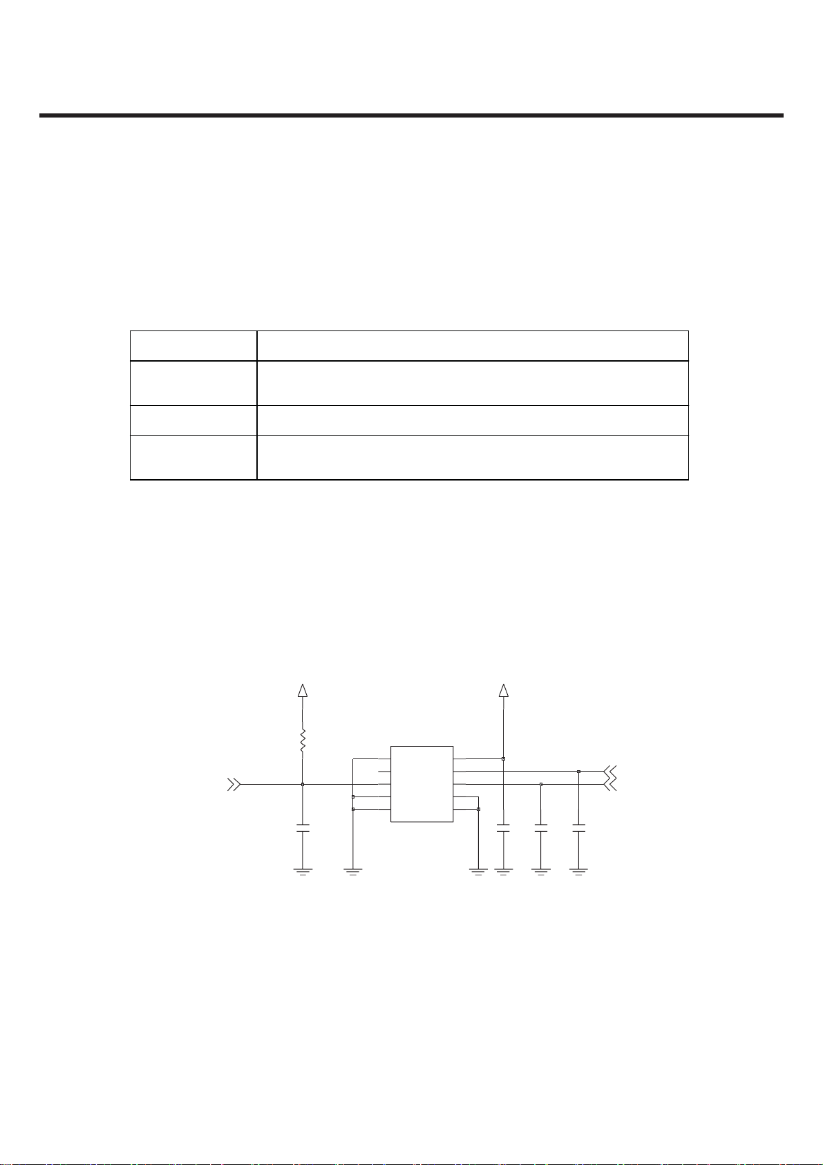
3.1 SKY77518 TX–RX iPAC™ FEM for Dual-Band GSM/GPRS
(SKY77518, U500)
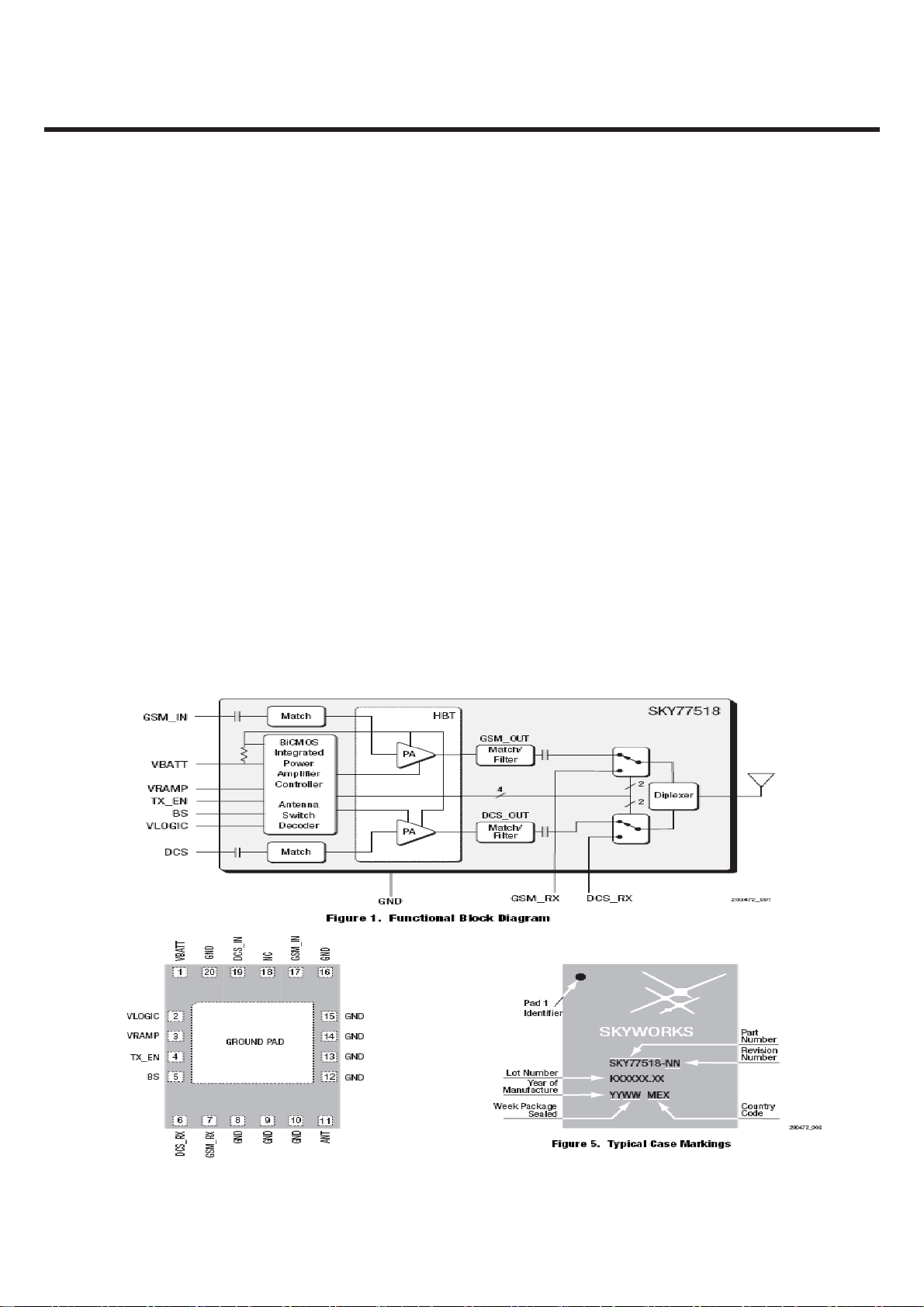
The SKY77518 is a transmit and receive front-end module (FEM) with Integrated PowerAmplifier Control
(iPAC™) for dual-band cellular handsets comprising GSM900 and DCS1800 operation. Designed in a low
profile, compact form factor, the SKY77518 offers a complete Transmit VCO-to-Antenna and Antenna-toReceive SAW filter solution. The FEM also supports Class 12 General Packet Radio Service (GPRS) multi-slot
operation. The module consists of a GSM900 PA block and a DCS1800 PA block, impedance-matching
circuitry for 50 Ω input and output impedances, TX harmonics filtering, high linearity and low insertion loss
PHEMT RF switches, diplexer and a Power Amplifier Control (PAC) block with internal current sense resistor. A
custom BiCMOS integrated circuit provides the internal PAC function and decoder circuitry to control the RF
switches. The two Heterojunction Bipolar Transistor (HBT) PA blocks are fabricated onto a single Gallium
Arsenide (GaAs) die. One PA block supports the GSM900 band and the other PA block supports the DCS1800
band. Both PA blocks share common power supply pads to distribute current. The output of each PA block
and the outputs to the two receive pads are connected to the antenna pad through PHEMT RF switches and a
diplexer. The GaAs die, PHEMT die, Silicon (Si) die and passive components are mounted on a multi-layer
laminate substrate. The assembly is encapsulated with plastic overmold. Band selection and control of
transmit and receive modes are performed using two external control pads. Refer to the functional block
diagram in Figure 1 below. The band select pad (BS) selects between GSM and DCS modes of operation. The
transmit enable (TX_EN) pad controls receive or transmit mode of the respective RF switch (TX = logic 1).
Proper timing between transmit enable (TX_EN) and Analog Power Control (VRAMP) allows for high isolation
between the antenna and TX-VCO while the VCO is being tuned prior to the transmit burst. The SKY77518 is
compatible with logic levels from 1.2 V to VCC for BS and TX_EN pads, depending on the level applied to the
VLOGIC pad. This feature provides additional flexibility for the designer in the selection of FEM interface
control logic.
Copyright © 2009 LG Electronics. Inc. All right reserved.
Only for training and service purposes
- 15 -
LGE Internal Use Only
3. TECHNICAL BRIEF
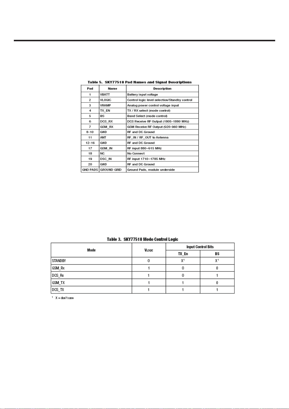
Table 5 Pad description
Table 3 Mode Control logic
LGE Internal Use Only Copyright © 2009 LG Electronics. Inc. All right reserved.
- 16 -
Only for training and service purposes
3. TECHNICAL BRIEF
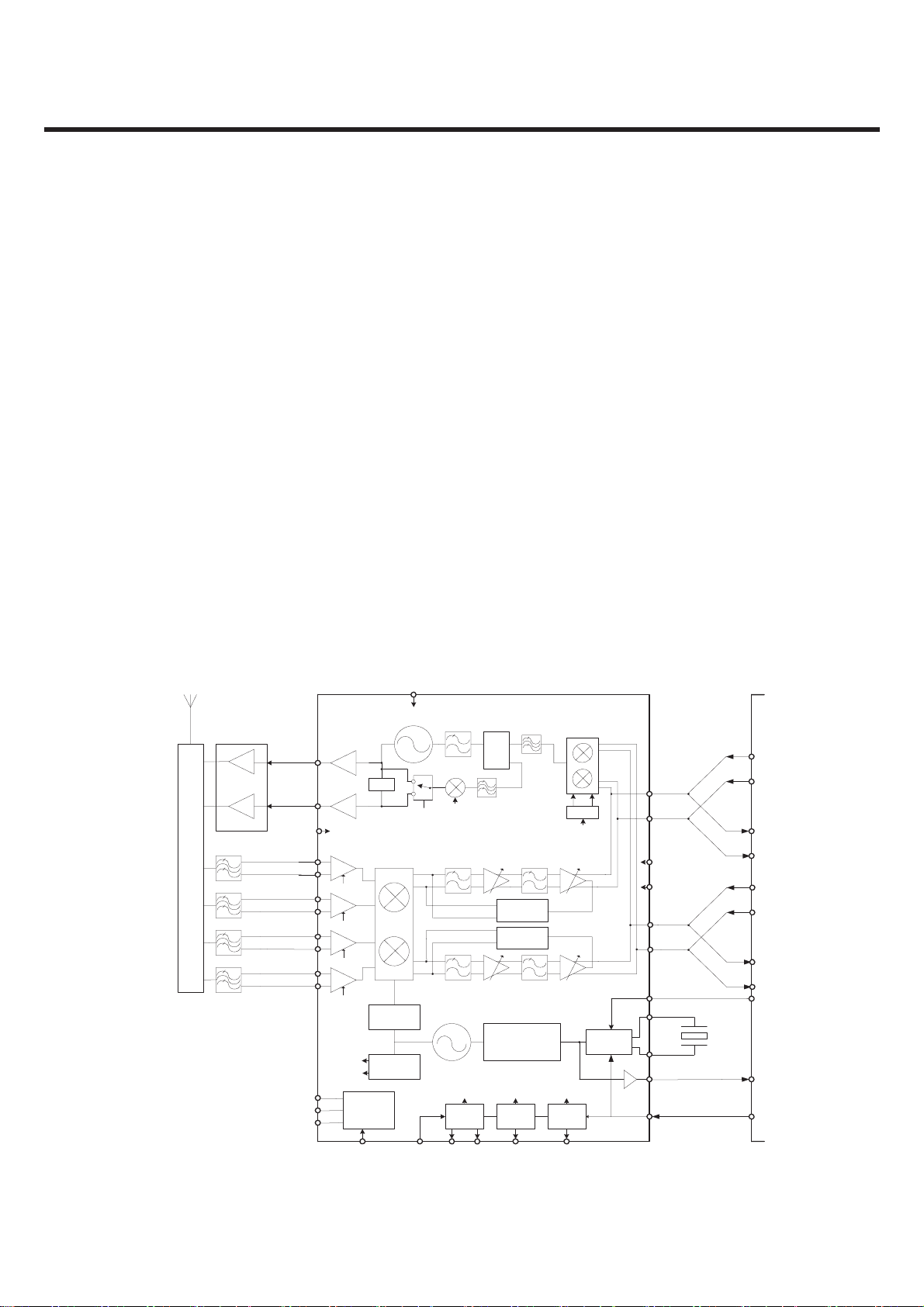
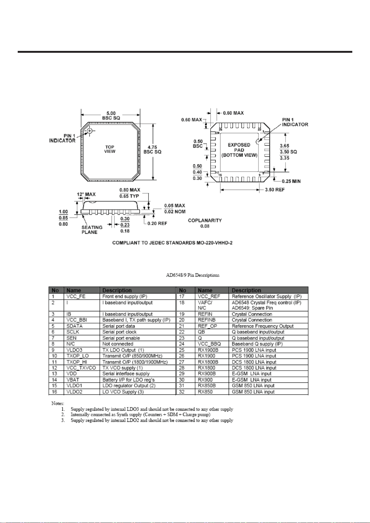
3.2 Transceiver (AD6548, U501)
The AD6548 provides a highly integrated direct conversion radio solution that combines, on a single chip,
all radio and power management functions necessary to build the most com-pact GSM radio solution
possible. The only external components required for a complete radio design are the Rx SAWs, PA,
Switchplexer and a few passives enabling an extremely small cost effective GSM Radio solution. The
AD6548 uses the industry proven direct conversion receiver architecture of the OthelloTM family. For Quad
band applications the front end features four fully integrated programmable gain differential LNAs. The RF
is then down converted by quad-rature mixers and then fed to the baseband programmable-gain
amplifiers and active filters for channel selection. The Receiver output pins can be directly connected to the
baseband analog processor. The Receive path features automatic calibration and tracking to remove DC
offsets. The transmitter features a translation-loop architecture for directly modulating baseband signals
onto the integrated TX VCO. The translation-loop modulator and TX VCO are extremely low noise removing
the need for external SAW filters prior to the PA. The AD6548 uses a single integrated LO VCO for both the
receive and the transmit circuits. The synthesizer lock times are optimized for GPRS applications up to and
including class 12.
AD6548 incorporates a complete reference crystal calibration system. This allows the external VCTCXO to
be replaced with a low cost crystal. No other external components are required. The AD6548 uses the
traditional VCTCXO reference source. The AD6548 also contains on-chip low dropout voltage regulators
(LDOs) to deliver regulated supply voltages to the functions on chip, with a battery input voltage of
between 2.9V and 5.5V. Comprehensive power down options are included to minimize power
consumption in normal use. A standard 3 wire serial interface is used to program the IC. The interface
features low-voltage digital interface buffers compatible with logic levels from 1.6V to 2.9V.
Antenna Switch Module
PA Module
GSM1800/1900
GSM850/900
TXOP_HI
TXOP_LO
VCC_FE
RX850
RX850B
RX900
RX900B
RX1800
RX1800B
RX1900
RX1900B
SDATA
SCLK
SEN
LNA Gain
Reduction
TX_LO2
TX_LO1
Generator
Generator
Serial
Interface
VCC_TXVCO
/2
RX LO
TX LO
Band
Control
TX Loop
Filter
TX_LO1
TX circuits
Reg 3
supply
LDO
PFD
DC Offset
Correction
DC Offset
Correction
Frac-N Synth
LO VCO
Supply
LDO
Reg 2
AD6548
General
Supply
LDO
Reg 1
/4
TX_LO2
Xtal Osc
+ Tuning
Supply
Ref
I
IB
VCC_BBI
VCC_BBQ
Q
QB
VAFC
REFINB
REFIN
REF_OP
VCC_REF
TXIB
TXI
RXI
RXIB
TXQ
TXQB
RXQ
RXQB
AFC
CLK
REF_OP
VDD
Figure 3.3 AD6548 Block Diagram
Copyright © 2009 LG Electronics. Inc. All right reserved.
Only for training and service purposes
VCC_
VBAT VLDO3 VLDO2 VLDO1
TXVCO
- 17 -
LGE Internal Use Only
3. TECHNICAL BRIEF
LGE Internal Use Only Copyright © 2009 LG Electronics. Inc. All right reserved.
- 18 -
Only for training and service purposes
3. TECHNICAL BRIEF
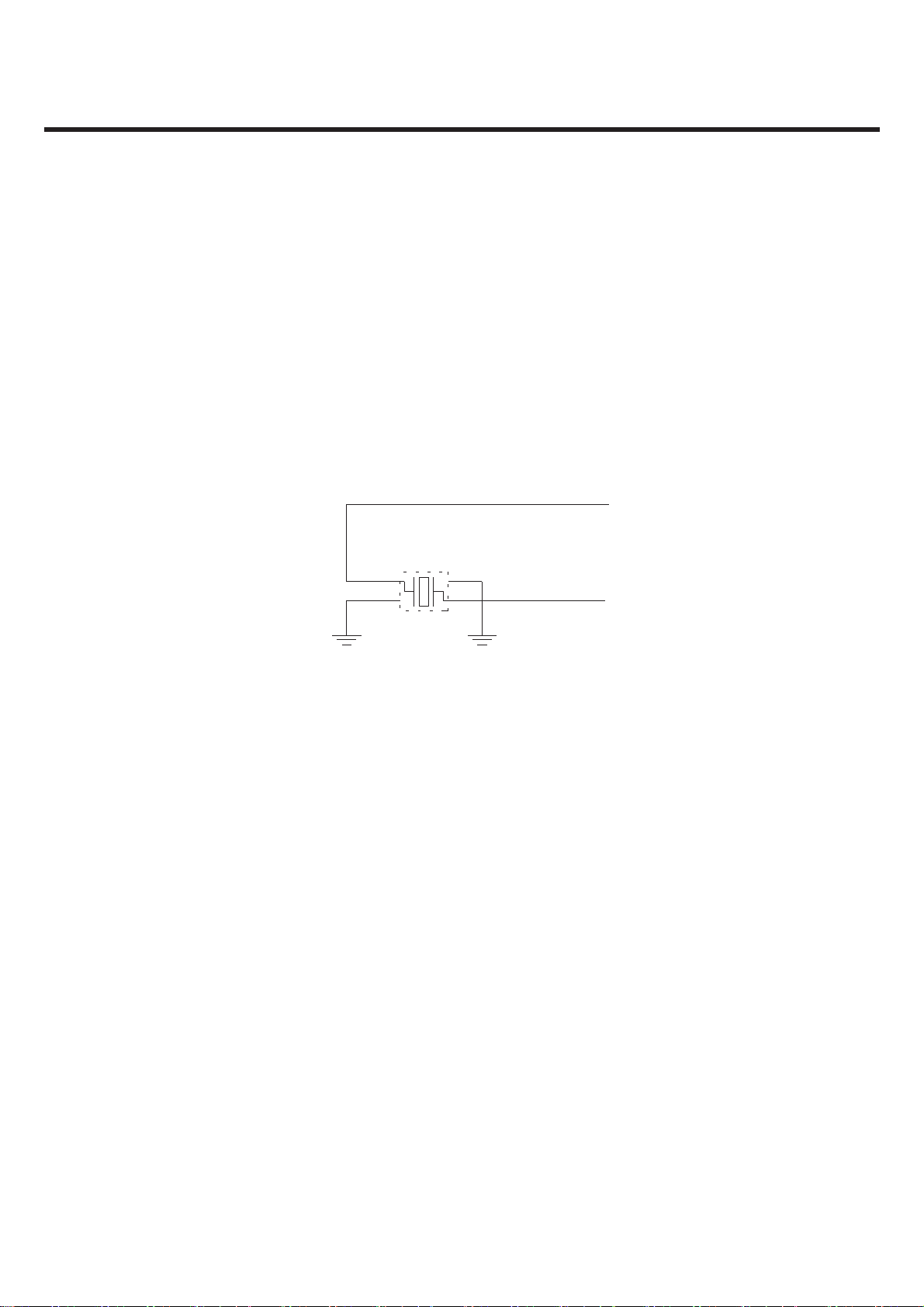
3.3 26 MHz Clock (Crystal, X500)
The 26 MHz clock (X401) consists of a XO (Crystal Oscillator) which oscillates at a frequency of 26 MHz. The
AD6548 requires only an external low cost crystal as the frequency reference. The circuitry to oscillate the
crystal and tune its frequency is fully integrated. The Oscillator is a balanced implementation requiring the
crystal to be connected across 2 pins. There is a programmable capacitor array included for coarse tuning of
fixed offsets (e.g. crystal manufacturing tolerance), and an integrated varactor for dynamic control. The
oscillator is designed for use with a 26MHz crystal. Dedicated control software ensures excellent frequency
stability under all circumstances.
X500
3
4
12
26MHz
DSX321G-26M
Figure 3.4 CRYSTAL CIRCUIT DIAGRAM
Copyright © 2009 LG Electronics. Inc. All right reserved.
Only for training and service purposes
- 19 -
LGE Internal Use Only

3. TECHNICAL BRIEF
3.4 BT Module with integrated FM tuner(BC5-FM, U200)
The BlueCore5-FM BGA is a single-chip radio and baseband IC for Bluetooth 2.4GHz systems
including enhanced data rates (EDR) to 3Mbits/s. It includes an integrated FM receiver with
stereo audio output stage and an RDS demodulator.
With the on-chip CSR Bluetooth software stack, it provides a fully compliant Bluetooth system
to v2.1 + EDR of the specification for data and voice communications.
LGE Internal Use Only Copyright © 2009 LG Electronics. Inc. All right reserved.
- 20 -
Only for training and service purposes

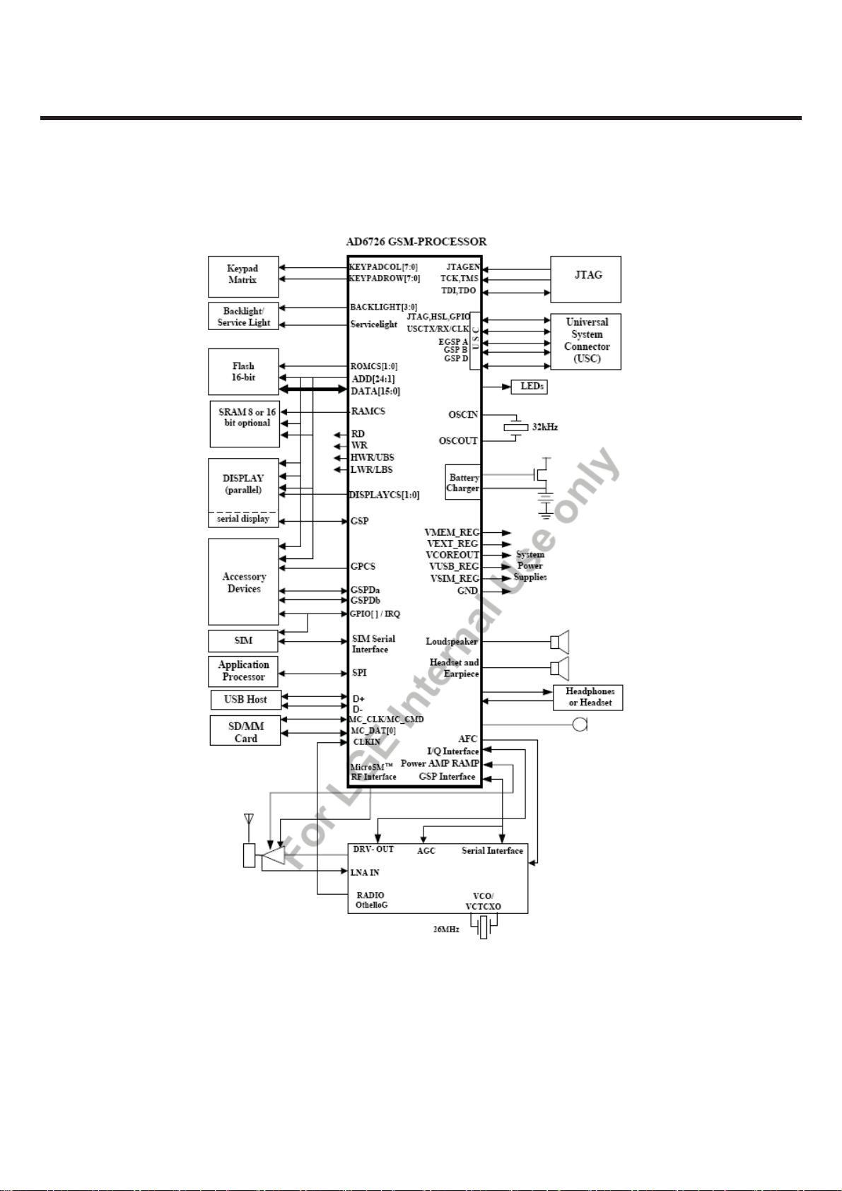
3.5 Baseband Processor (AD6726 , U103)
• AD6726 is an ADI designed processor
•AD6726 consists of
1. Control Processor Subsystem including:
32-bit MCU ARM7TDMI® Control Processor
78 MHz operation at 1.8V
2Mb of on-chip System SRAM Memory
2.DSP Subsystem including:
16-bit Fixed Point DSP Processor
91 MIPS[1] at 1.8V
Data and Program SRAM
Program Instruction Cache
Full Rate, Enhanced Full Rate and Half Rate
Speech Encoding/Decoding
Capable of Supporting AMR & PDC Speech Algorithms
3. TECHNICAL BRIEF
3.Peripheral Functions
Parallel and Serial Display Interface
USB 2.0 Full Speed device Interface
Keypad Interface
Support for Burst and Page Mode Flash
1.8V and 3.0V, 64 kbps SIM Interface
Universal System Connector Interface
Data Services Interface
SD/Multimedia Card Interface
4. Other
Supports 13 MHz and 26 MHz Input Clocks
1.8V Typical Core Operating Voltages
361-Ball Package (13x13mm) , 0.65mm Ball pitch
5. The AD6726 baseband transmit section supports the following
mobile station GMSK modulation power classes:
GSM 900/850 power classes 4 and 5,
DCS 1800 power classes 1 and 2, and
PCS 1900 power classes 1 and 2
Copyright © 2009 LG Electronics. Inc. All right reserved.
Only for training and service purposes
- 21 -
LGE Internal Use Only
3. TECHNICAL BRIEF
Figure 3.5 SYSTEM INTERCONECTION OF AD6726 EXTERNAL INTERFACE
LGE Internal Use Only Copyright © 2009 LG Electronics. Inc. All right reserved.
- 22 -
Only for training and service purposes
3.5.1 Interconnection with external devices
A. RTC block interface
Countered by external X-TAL
32.768kHz oscillator supplies on-chip Real Time Clock circuitry
B. LCD module interface
The LCD module is controlled via mobile media processor AIT716
If AIT716 is in the state of by-pass mode, the LCD control signals from AD6726
are by-passed through AIT716.
In operating mode, the AIT716 controls the LCD module through nLCD_CS, nLCD_RS,
nLCD_WR, L_DATA08~L_DATA15.
Signals Description
3. TECHNICAL BRIEF
nLCD_CS
LCD_ID
LCD_RESET
nLCD_WR
nLCD_RS
2V8_MM
MAIN LCD driver chip enable. MAIN LCD driver IC has own CS pin
Identify LCD module maker
This pin resets LCD module. This signal comes from AD6726 directly.
Enable writing to LCD Driver.
This pin determines whether the data to LCD module are LCD command
or data.
2.8V is supplied to LCD driver IC.
Table 3.5.B LCD CONTRON SIGNALS DISCRIPTION
Copyright © 2009 LG Electronics. Inc. All right reserved.
Only for training and service purposes
- 23 -
LGE Internal Use Only

3. TECHNICAL BRIEF
The backlight of LCD module is controlled by AD6726 via AAT2845.
The control signals related to Backlight LED are given as follows.
Signals Description
MLED
LCD_DIM_CTRL
MLED[1:2]
Table 3.5.B2 DESCRIPTION OF LCD BACKLIGHT LED CONTROL
C. RF interface
The AD6726 control RF parts through PA_BAND, ANT_SW, CLKON , PA_EN, S_EN, S_DATA, S_CLK
Current source for backlight LED
Control LCD backlight level in 16 steps
This pins are returned-paths for backlight LED current
source (MLED)
DescriptionSignal
PA_BAND (GPIO 0)
PAM Band Select
Antenna switch Band SelectANT_SW (GPO 9)
PA_EN (GPO 16)
Table 3.5.C RF CONTROL SIGNALS DESCRIPTION
LGE Internal Use Only Copyright © 2009 LG Electronics. Inc. All right reserved.
PAM Enable/Disable
PLL Enable/DisableS_EN (GPO 19)
Serial Data to PLLS_DATA (GPO 20)
Clock to PLLS_CLK (GPO 21)
- 24 -
Only for training and service purposes
3. TECHNICAL BRIEF
K
D. SIM interface
The AD6726 provides SIM Interface Module. The AD6726 checks status periodically during
established call mode whether SIM card is inserted or not, but it doesn't check during deep
Sleep mode. In order to communicate with SIM card, 3 signals SIM_DATA, SIM_CLK,
SIM_RST(GPIO_23) are required. The descriptions about the signals are given by bellow Table 3-5 in detail.
Signals Description
SIM_DATA
SIM_CLK
SIM_RST
(GPIO_23)
This pin receives and sends data to SIM card.
This model can support 3.0 volt and 1.8 volt interface SIM card.
Clock 3.25MHz frequency.
Reset SIM block
Table 3.5.D SIM CONTROL SIGNALS DESCRIPTION
SIM_CONNECTOR
2V85_VSIM
R303
15K
SIM_DATA
C306
DNI
2V85_VSIM
J300
4
C5
5
C6
6
C7
10
GND4
9
C1
C2
C3
GND1
GND2GND3
1
2
3
7
8
C304
C307
220n
DNI
SIM_RST
SIM_CL
C308
1000p
Figure 3.5.D2 SIM Interface of AD6726
Copyright © 2009 LG Electronics. Inc. All right reserved.
Only for training and service purposes
- 25 -
LGE Internal Use Only

3. TECHNICAL BRIEF
E. LDO Block
There are 9 LDOs in the AD6726.
- 1V8_VCORE : supplies Digital baseband Processor core and AD6726 digital core(1.8V, 80mA)
- 2V8_VMEM : supplies external memory and the interface to the external memory on the digital
baseband processor (2.8V, 150mA)
- 2V8_VEXT : supplies Radio digital interface and high voltage interface (2.8V, 200mA)
- 2V85_VSIM : supplies the SIM interface circuitry on the digital processor and SIM card
(2.85V,1.8V, 20mA)
- 1V8_VRTC : supplies the Real-Time Clock module (1.8 V, 20 μA)
- 2V5_VMIC : supplies the microphone interface circuitry (2.5 V, 2 mA)
- 2V75_VVCXO: supplies the voltage controlled crystal oscillator ( 2.75 V, 10 mA)
- VUSB : supplies USB interface circuitry( 3.2V, 20mA)
- 1V8_VGP : supplies VDD_IO1 & VDD_IO4 of MMP(1.8V, 40mA)
LGE Internal Use Only Copyright © 2009 LG Electronics. Inc. All right reserved.
- 26 -
Only for training and service purposes
3. TECHNICAL BRIEF
3.6 Display and Interface
UnitSpec.Properties
mm28.032mm(W) x 35.04mm(H)Active Screen Size
colors262K TFTColor Depth
Pixels128 X 160Resolution
Controlled by nLCD_CS, LCD_RESET, nLCD_RS, nLCD_WR, L_DATA08~L_DATA15
• nLCD_CS : MAIN LCD driver chip enable. MAIN LCD driver IC has own CS pin
• LCD_RESET : This pin resets LCD module. This signal comes from AD6726 directly.
• nLCD_RS: This pin determines whether the data to LCD module are display data or control data.
• nLCD_WR : Write control Signal
• L_DATA08~L_DATA15 : Parallel data lines.
•LCD_ID : reserved
1
nLCD_RS
nLCD_WR nLCD_WR_OUT
VSYNCOUT VSYNCOUT_
nLCD_CS nLCD_CS_OUT
INOUT_A1
2
INOUT_A2
3
INOUT_A3
4
INOUT_A4
INOUT_B1
INOUT_B2
INOUT_B3
INOUT_B4
G110G2
5
9
8
7
6
nLCD_RS_OUT
FL301 ICVE10184E150R101FR
ICVE10184E150R101FRFL300
L_DATA15
L_DATA14
L_DATA13
L_DATA12
1
INOUT_A1
2
INOUT_A2
3
INOUT_A3
4
INOUT_A4
INOUT_B1
INOUT_B2
INOUT_B3
INOUT_B4
G15G2
10
9
8
7
6
DATAOUT15
DATAOUT14
DATAOUT13
DATAOUT12
ICVE10184E150R101FRFL302
L_DATA10
L_DATA09
L_DATA08
1
INOUT_A1
2
INOUT_A2
3
INOUT_A3
4
INOUT_A4
INOUT_B1
INOUT_B2
INOUT_B3
INOUT_B4
G110G2
5
9
8
7
6
DATAOUT11L_DATA11
DATAOUT10
DATAOUT09
DATAOUT08
Copyright © 2009 LG Electronics. Inc. All right reserved.
Only for training and service purposes
- 27 -
LGE Internal Use Only
3. TECHNICAL BRIEF
MLED
MLED1
MLED2
VSYNCOUT_
nLCD_RD_OUT
nLCD_WR_OUT
nLCD_RS_OUT
LCD_RESET_OUT
nLCD_CS_OUT
DATAOUT15
DATAOUT14
DATAOUT13
DATAOUT12
DATAOUT11
DATAOUT10
DATAOUT09
DATAOUT08
LCD_ID
IM2
IM1
R331
20K
2V8_MM
CN305
35
34
33
32
31
30
29
28
27
26
25
24
23
22
21
20
19
18
17
16
15
14
13
12
11
10
9
8
7
6
5
4
3
2
1
C349
1u
Figure 3.6 LCD INTERFACE CIRCUIT
LGE Internal Use Only Copyright © 2009 LG Electronics. Inc. All right reserved.
- 28 -
Only for training and service purposes
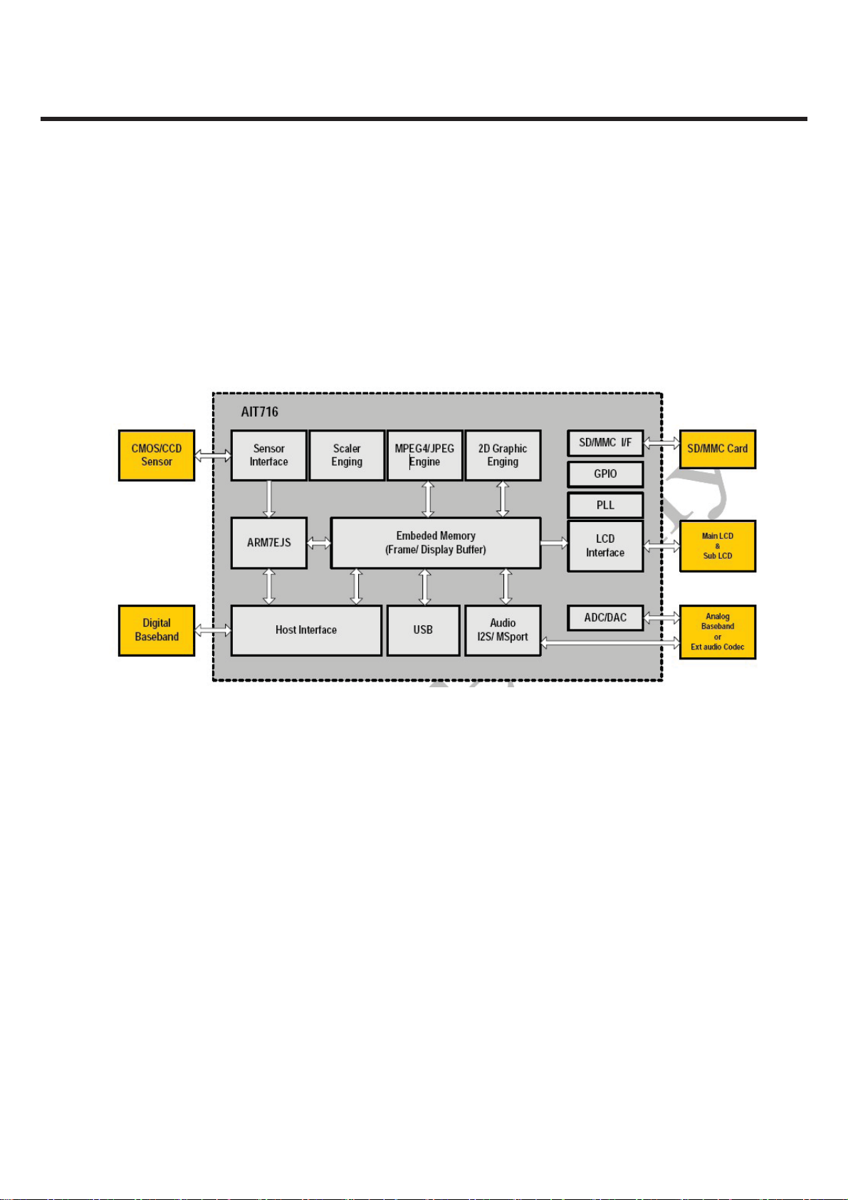
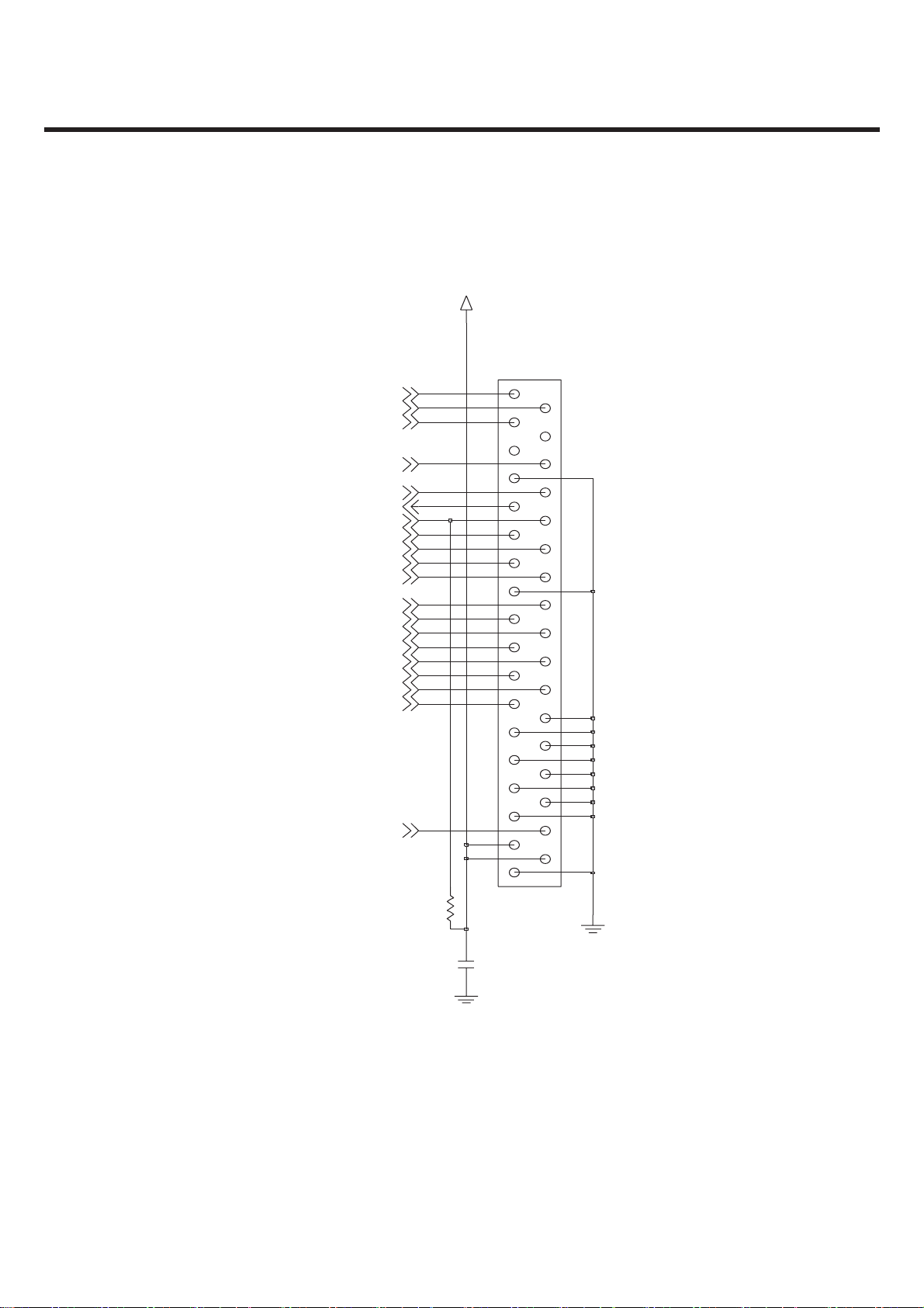
3.7 Camera Interface(AIT716 , U400)
This model has a built-in 1.3M SXGA (1280 x 1024) camera module. And the camera produces
JPG pictures. Camera module is controlled by AIT716. Interface is done by I2C and
YCbCr format. I2C is a control signal and YCbCr is real data interface signal.
3. TECHNICAL BRIEF
Figure 3.7.1 AIT716 BLOCK DIAGRAM
Copyright © 2009 LG Electronics. Inc. All right reserved.
Only for training and service purposes
- 29 -
LGE Internal Use Only
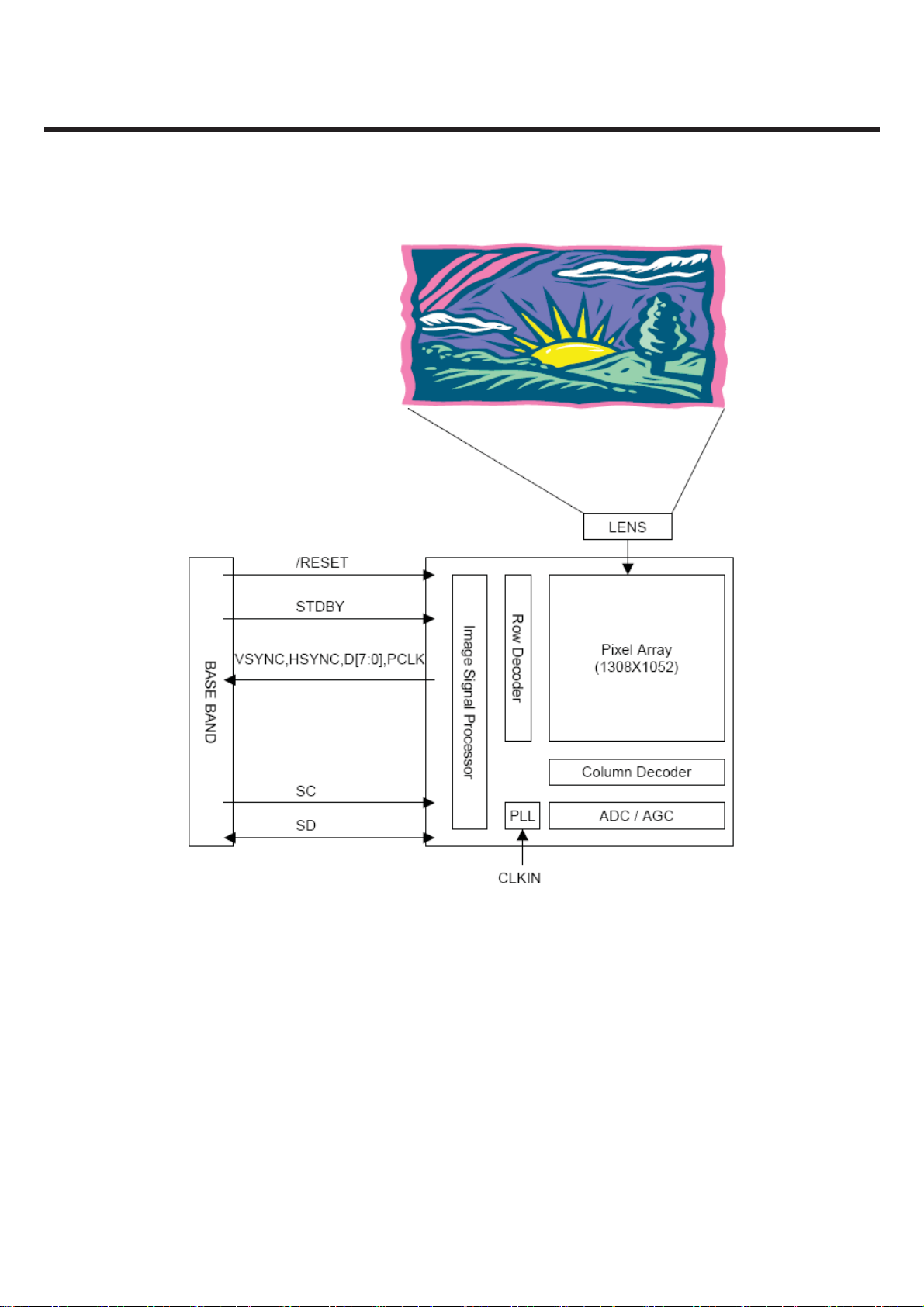
3. TECHNICAL BRIEF
Figure 3.7.2 SENSOR CHIP BLOCK DIAGRAM
LGE Internal Use Only Copyright © 2009 LG Electronics. Inc. All right reserved.
- 30 -
Only for training and service purposes
2V8_MM
3. TECHNICAL BRIEF
_MAIN_CS
_MULTI_RST
MULTIMEDIA IC
C407
33p
ADD01
_RD
_WR
DATA00
DATA01
DATA02
DATA03
DATA04
DATA05
DATA06
DATA07
R406 0
2V8_MM
R402
100K
LCD_BYPASS
_MULTI_INT
13M_AIT
26MHz_BT
nCAM_RST
DATA400
BYPASS
ADD400
MULT_INT
_WAIT
DNIR407
C1
C2
B3
B1
B5
D1
D2
C3
D3
D4
E1
E2
E3
F1
F2
F3
B6
G1
A6
F9
F10
F8
E10
G8
PHCS_
PHRD_
PHWE_
PRST_
PHD0
PHD1
PHD2
PHD3
PHD4
PHD5
PHD6
PHD7
PHD8
PHLCD_BY
PHLCD_A0
PHLCD2_CS_
PHINT
PHWAIT_
PMCLK
PI2S_SCK
PI2S_WS
PI2S_SDO
PI2S_MCLK
NC1
1V8_VGP
1V2_VMM
C400
1u
E5
G6
VDD_CORE0
VDD_CORE1E6VDD_CORE2
Ball Name is changed(E6,F4)
PVSYNC
PHSYNC
G2
G3
F4
VDD_CORE3
PD2
PD3
H1
G4
C401
PD4C5PD5
H2
1u
E4
F5
VDD_IO0
H3
3V3_VUSB
VDD_IO1J8VDD_IO2
PD6
G5
D7
VDD_IO3A1VDD_IO4E7VDD_IO5
PD9
PD7
PD8
J1
J3
H4
C402
C403
1u
39p
D5
F6
H5
GND_IO1
GND_IO2B2GND_IO3F7GND_IO4D6GND_IO5
GND_IO0
EUSY0344901
U400
AIT716
PSCK
PSDAJ2PSEN
PDCLK
PPXL_CLK
J4
K2
K1
C404
1u
PLCD0K3PLCD1
PLCD2
J9
H6
G7
AVD D
PLCD3
J10
1V2_VMM
H7
AVS S
PLCD4J6PLCD5
K4
C405
1u
B4
A5
VSS_PLL
VDD_PLL
PLCD6
PLCD7
J5
K6
PLCD8
K5
C4
K7
1
R400
C6
A8
VDD_CLK
GND_CLK
PLCD_A0K8PLCD_RD_
PLCD_WE_
J7
K10
C406
1u
A4
PTEST_EN
PSCAN_EN
PGPIO0
PGPIO1
PGPIO2
PGPIO3
PGPIO4
PGPIO5
PGPIO6
PGPIO7
PGPIO8
PGPIO9
PGPIO10
PGPIO11
PGPIO12
PGPIO13
PGPIO14
PGPIO15
PVIN_P
PVIN_N
PVREF_P
PVREF_N
NC2
PUSBDN
PUSBDP
PLCD1_CS_
PLCD2_CS_
K9
E9
E8
D10
D9
D8
C8
C9
C10
C7
B8
R403 DNI
B9
B10
B7
A10
A7
A9
G10
H10
Single-end strero MIC Input(AIT)
H8
H9
G9
A3
A2
DNIR404
C415 0.1uF
0.1uFC416
R405 12K
TF_CLK
TF_CMD
TF_DATA0
TF_DATA1
TF_DATA2
TF_DATA3
TF_DET
TF_EN
VSYNCOUT
AIT_UART_RX
AIT_UART_TX
FM_L
FM_R
MM_MICP
MM_L
MM_R
MM_USBDM
MM_USBDP
C417
10u
1V8_CAMIO
C_VS_OUT
C_HS_OUT
C_CD00_OUT
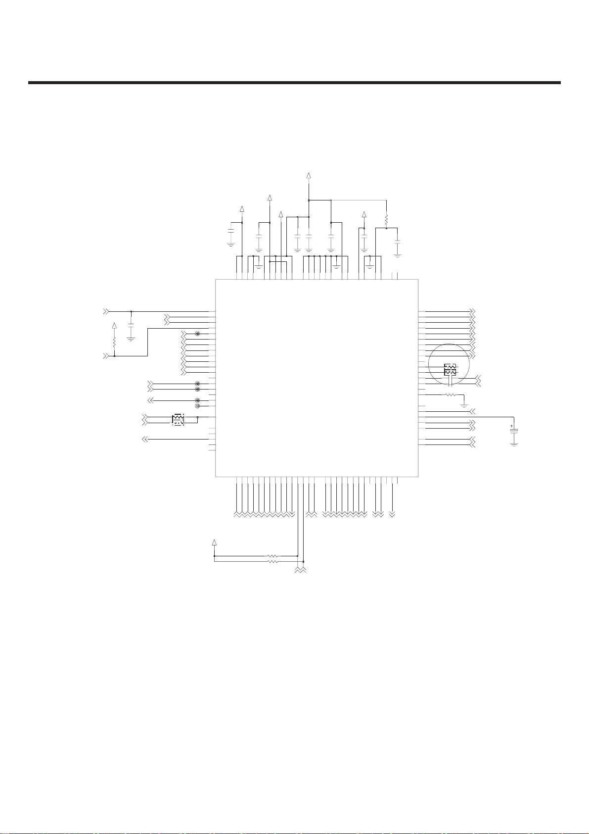
Figure 3.7.3 AIT716 CIRCUIT
Copyright © 2009 LG Electronics. Inc. All right reserved.
Only for training and service purposes
C_CD01_OUT
C_CD02_OUT
C_CD03_OUT
C_CD04_OUT
R417 4.7K
C_CD05_OUT
C_CD06_OUT
C_CD07_OUT
CAM_PWR_EN
4.7KR416
- 31 -
C_SDA
C_MCLK
C_SCK
L_DATA08
L_DATA09
C_PCLK_OUT
nLCD_RS
nLCD_CS
L_DATA10
L_DATA11
nLCD_WR
L_DATA12
L_DATA13
L_DATA14
L_DATA15
LGE Internal Use Only
 Loading...