

LG GB125 Service Manual
1
LG Electroni
cs
GB125
GB125
GB125GB125
Service Manual
Service Manual
Service ManualService Manual

2
Table Of Contents
1. INTRODUCTION…………………..3
1.1 Purpose…………………………………..3
1.2 Regulatory Information………………….3
2. PERFORMANCE…………………...5
2.1 H/W Features…………………………….5
2.2 S/W Features……………………………..6
3. TECHNICAL BRIEF………………11
3.1 Digital Main Processor( PMB7880)…….11
3.2 Power Amplifier Module
3.3 26 MHz Clock (DCXO)…………….…...21
3.4 RTC(32.768KHz Crystal)………...……..22
3.5 LCD Interface……………………..…….23
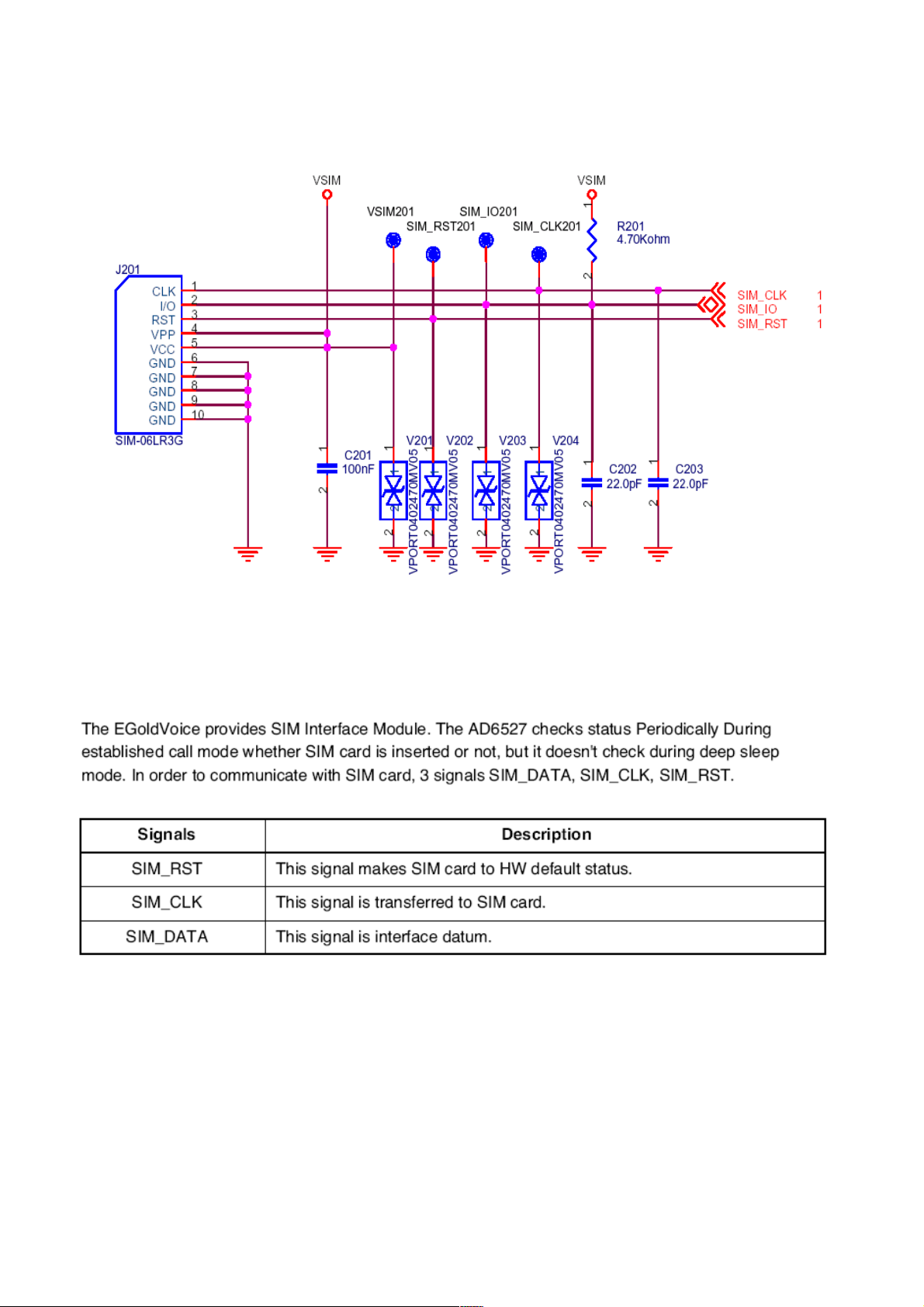
3.6 SIM Card Interface……………………...24
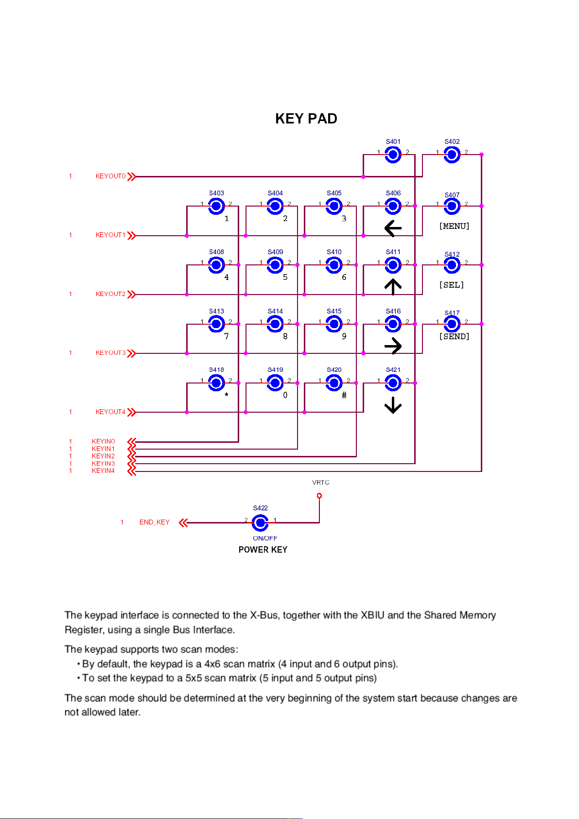
3.7 KEYPAD Interface……………………...25
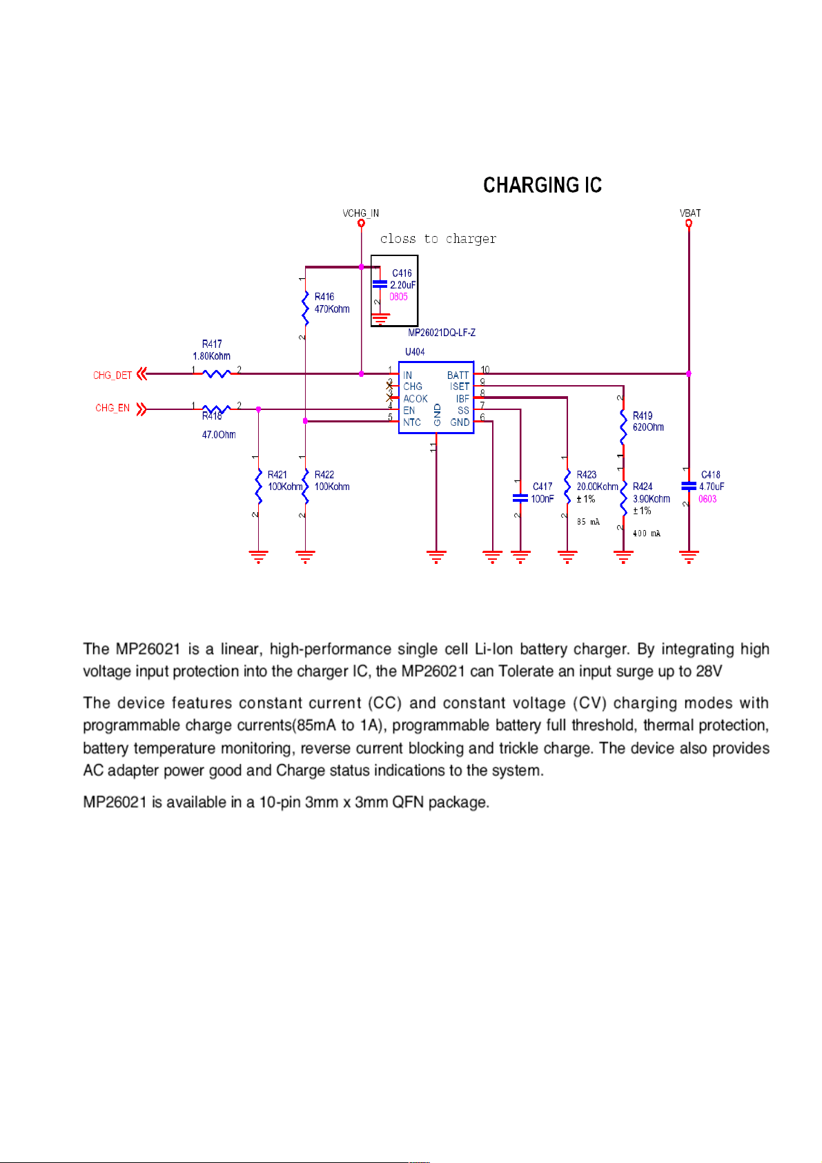
3.8 Battery Charging Block Interface…….…26
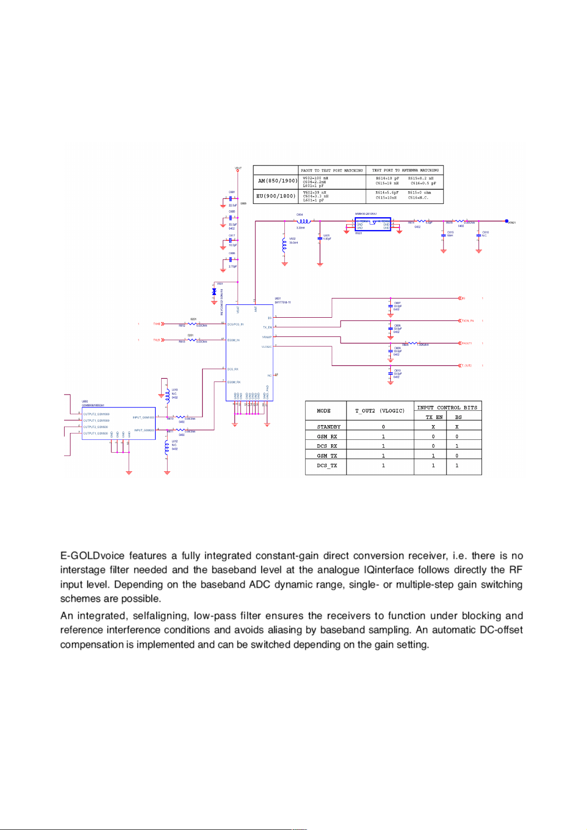
3.9 RF Interface………………………....…..27
3.10 Audio Interface…………………….…..29
(SKY77318/SKY77317)
18
4.13 Speaker Trouble………………………..71
4.14 Headphone Trouble…………………….73
4.15 Charging Trouble………………………76
4.16 FM Radio Trouble……………………..78
5. DOWNLOAD………………………82
5.1 Download setup…………………………82
5.2 Download Process……………………….83
6. BLOCK DIAGRAM……………….96
7. CIRCUIT DIAGRMA……………..97
8. BGA IN PIN Check……………….102
9. PCB LAYOUT…………………….104
10.ENGINEERING MODE…………106
3.11 Key LED Interface……………….…….31
3.12 Vibrator Interface………………….…...32
3.13 Memory Interface……………………...33
3.14 Power Block Interface…………….……34
3.15 FM Radio Interface…………………….36
4. TROUBLE SHOOTING…………..38
4.1 RF Trouble………………………………38
4.2 TX Trouble………………………….…...44
4.3 Power On Trouble……………………….50
4.4 SIM Card Trouble……………………….53
4.5 Vibrator Trouble…………………………55
4.6 Keypad Trouble………………………….57
4.7 RTC Trouble……………………………..59
4.8 Key Backlight Trouble…………………..61
4.9 LCM Backlight Trouble…………………63
4.10 LCD Trouble…………………………...65
4.11 Microphone Trouble……………………67
11.CALIBRATION…………………..108
11.1 Test equipment setup…………..……...108
11.2 APT Technologies…………………….108
12. Stand alone test…………………..123
12.1 Test Program Setting………………….123
12.2 TX Test ……………………………....126
12.3 RX Test……………………………….127
13. EXPLODED VIEW&
REPLACEMENT PART LIST……..128
13.1 Exploded View………………………..128
13.2 Replacement Part……………………..130
4.12 Receiver Trouble……………………….69

3
1. INTRODUCTION
1.1 Purpose
This manual provides information necessary to repair, description and download the features of this
model.
1.2 Regulatory Information
A. Security
Toll fraud, the unauthorized use of telecommunications system by an unauthorized part(for
example ,persons other than your company’s employees, agents, subcontractors, or person working
on your company’s behalf) can result in substantial additional charges for your telecommunications
services.
system users are responsible for the security of own system. There are may be risks of toll fraud
associated with your telecommunications system. System users are responsible for programming
and configuring the equipment to prevent unauthorized use .The manufacturer dose not warrant that
this product is immune from the above case but will prevent unauthorized use of common-carrier
telecommunications service of facilities accessed through or connected to it.
The manufacturer will not be responsible for any charges that result from such unauthorized use.
B. Incidence of Harm
If a telephone company determines that the equipment provided to customer is faulty and possibly
causing harm or interruption in service to the telephone network, it should disconnect telephone
service until repair can be done. A telephone company may temporarily disconnect service as long
as repair is not done.
C. Changes in Service
A local telephone company may make changes in its communications facilities or procedure. If
these changes could reasonably be expected to affect the use of the this phone or compatibility with
the network, the telephone company is required to give advanced written notice to the user,
allowing the user to take appropriate steps to maintain telephone service.
D. Maintenance Limitations
Maintenance limitations on this model must be performed only by the manufacturer or its
authorized agent . The user may not make any changes and/or repairs expect as specifically noted in
this manual.

4
Therefore, note that authorized alternations or repair may affect the regulatory status of the system
and may void any remaining warranty.
E. Notice of Radiated Emissions
This model complies with rules regarding radiation and radio frequency emission as defined by
local regulatory agencies. In accordance with these agencies, you may be required to provide
information such as the following to the end user.
F. Pictures
The pictures in this manual are for illustrative purposes only; your actual hardware may look
slightly different.
G. Interference and Attenuation
Phone may interfere with sensitive laboratory equipment, medical equipment, etc. Interference
from unsuppressed engines or electric motors may cause problems.
H. Electrostatic Sensitive Devices
ATTENTION
Boards, which contain Electrostatic Sensitive Devices(ESD),are indicated by the sign .
Following information is ESD handing:
. Service personnel should ground themselves by using a wrist strap when exchange system boards.
. When repairs are made to a system board , they should spread the floor with anti-static mat which
is also grounded .
. Use a suitable, grounded soldering iron .
. Keep sensitive parts in these protective packages until these are used.
. When returning system boards or parts like EEPROM to the factory, use the protective packages
as described.
5
2. PERFORMANCE
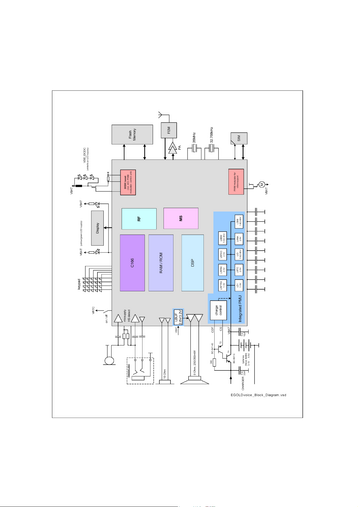
2.1 H/W Features
Solution EGOLD voice PMB7880 (ULC2) Infineon
Type Folder type
Antenna Type Internal (dual-Band)
Main Display 1.5” 128x128 CSTN/65k
Battery 950mAh Li-ion inner pack 950mAh: (55x34x50mm)
Audio player MIDI ring tone, 16poly MIDI ring tone
FM Receiver
Embedded FM antenna Yes
Loud Speaker Yes 18*13(4.05T) Recheck
Memory Size 32Mb+4Mb No user memory
LMT (Lost Mobile Tracker) Yes
Yes , US/Europe band support
(Optional) (87.5 88~108MHz) Recheck
Pogo pin contact FPC type
FM Antenna on Battery
cover.
Asia, Middle East, Africa:
LMT Support
China: M-DOG
CIS: Based on CIS CA
requirement
LA: Based on operator
request
EU: Based on operator
request

6
2.2 S/W Features
Feature Detail Item Description
OS OSE Operating System Y
Audio
y Bands
Speech Code FR,EFR,HR,AMR-NB Y
AMR code GSM Full Rate
3GPP Adaptive Multi Rate (AMR-NB)
FM Radio Y
MP3 Ring Tone MP3 decode N
Integrated hands free
speaker
Key Tone Volume 6 Level (Include Mute) Y
Ring Tone Volume 6 Level (Include Mute) Y
Ring Tone 10 Midi Y
Call Alert type Ring, Vibrate, Ring & Vibrate, Ring after vibrate, Silent Y
Earpiece Volume 6 Level (Include Mute) Y
Mute Y
GSM dual band MS
900-1800
PCS dual band MS
Speaker phone mode Y
Y Frequenc
Configuration is during software compile time. Y
Y
Service
Connecti
vity
Voice
Function
Display
850-1900
Circuit N Date
Packet N
Infrared (IrDA) N
Bluetooth N
USB N
USB Mass storage N
RS232(UART) Only for Phone tool & download Y
Voice Recording N
Voice Command N
Answering machine N
RSSI 6 level (0~5Level) Y
Battery level 4 level (0~3Level) Y
RTC Date & Time Display Y
PLMN/Service
Indicator
Y

7
Call
History
Call
Manage
Quick Access Mode
In Idle
Dimming mode Y
Dual Clock N
Home shortcut Display Shortcut icon in Idle Y
Last Dial Number Max : 20 records Y
Last Received
Number
Last Missed Number Max : 20 records Y
Scratch Pad Memory N
Call Duration Last Call time, Total Call Time Y
Last Call Charge
Units
Total Charge Units N
Call Waiting Y
Call Swap Y
Profile/ SMS + Voice Mail Y
Max : 20 records Y
N Call Cost
ment
Network
Call Retrieve Y
Auto Answer Y
Auto Redial Y
Calling Line Y
Full Call Divert Y
Speed Dialing Y
Last Number Redial Y
Multi Party Call Y
ECT Explicit Call Transfer (4 + Send) N
Automatic Network
Selection
Manual Network Y
Preferred Network Y
Network Service
Status
DTMF Signaling Y DTMF
Y
Y
Cell
Broadcas
t
DTMF Enable &
Disable
Read Cell Broadcast Y
On/Off setting Receive On/Off Y
Alert setting Y
Y

8
Language setting Y
Topics Setting Y
Contacts(
Phone
Book)
Supplementary
Services
Entry Phone 300 + SIM Y
Field Name, Mobile, Home, Office Y
Copy ME <-> SIM Y
Move ME <-> SIM , Y
FDN Y
SDN Y
Email Entry N
Picture ID N
Video Caller ID N
vCard N
Business Card Y
Delete Delete, Delete All(SIM or Phone), Multi Delete Y
CFU Call Forwarding Unconditional Y
CFB Call Forwarding on Mobile Subscriber Busy Y
CFNRy Call Forwarding on No Reply Y
SIM
Short
Message
CFNRc Call Forwarding on Mobile Subscriber Not Reachable Y
BAOC Barring of All Outgoing Calls Y
BOIC Barring of Outgoing International Calls Y
BOICexHC Barring of Outgoing International Calls except those
directed to the Home PLMN Country
BAIC Barring of All Incoming Calls Y
BICRoam Barring of Incoming Calls when Roaming Outside
the/Home PLMN Country
Conference Call Upto 5 calls + 1 Waiting Call. Y
Plug in Type 3V & 1.8 V Y
SIM Lock Service Provider / Network Lock / Hard Lock Y
SIM Toolkit Support Class 1 to 3 Y
Read Message Y
Write and Edit
Message
Send and Receive
Y
Y
Y
Y
Message
Reply to Message Y
Forward Message Y

9
Extract Number from
Message
Message Status Y
Message Unread Y
Settable Message
Center Number,
Reply Path and
Validity
Visible and Audible
Message Receive
Voice Mail Y
Settable Voice Mail
Center Number
Message Protocol Normal, Fax, National Paging, X400,
Message Overflow
Y
Y
Y
Y
Y
ERMES, Voice
Y
Miscellaneous
Function
Input
Indicator
Message Center
Number
Nokia Smart Message
Development & Test
Facility
Field Test Facility Y
Display Software
Version
IMEI Y
Restore Factory
Setting
Battery Charging
Mode
Language Selectable Auto Language Y Text
Predictive word input T9 Y
Y
Not supported.
[Can be supported based on operator request]
Y
Y
Y
Y
N
Schedule
r
World Setting Local Time Y
Calendar MAX: 20 records (18 chars) Y
To Do N
Memo MAX: 10 records (80 chars) Y

10
Time
Unit
converter
Stop
Watch
Calculato
r
Game Will use Ruby’s Game, 1 game Y
Security
Display Two
Cities Time
Daylight saving Y
NITZ Y
Length, Weight, Volume, Surface,
Y
+ - * / Y
Phone Book Sync Only For service Center Y PC Sync
Message Sync N
Emergency Call Y
Handset Lock Y
Security Code When Delete All Y
Dual Clock N
Velocity, Temperature, User-defined
Y
SIM Lock Y
Keypad Lock Y
Real
Time
Clock
Accessor
y
Stereo earmic with
12/24 Hour Y
Calendar Y
Time Zone Y
Daylight saving Y
Alarm Manager Y
Dimming Clock N
Power-off Alarm Y
On Alarm Event Y
Mobile Tracking
software
M-DOG For China Y
microSD Adapter N
For India, Asia Y Others
Earmic type Sterio with hook key.
Y
hook switch
Only FM play supports Stereo.
11
3. TECHNICAL BRIEF
3.1 Digital Main Processor
Figure.3-1 PMB7880 FUNCTIONAL BLOCK DIAGRAM
12

13
3.1.2 Features
Baseband
• High performance fixed-point TEAKlite DSP
• C166S high performance microcontroller
• There are several Interfaces:
– I2S interface for DAI connections (for Tape Approval)
– High Speed SSC Interface for connection of external peripherals
– SIM Interface
– Keypad Interface (6x4 or 5x5 keys)
– EBU for external RAM/FLASH connection
– Asynchronous serial interface (incl. IrDA support capability)
– JTAG Interface
– Black & white and color displays are supported
– PWM source to drive vibrator
– Keypad and display backlight supported.
Receiver
• Constant gain, direct conversion receiver with fully integrated blocking filter
• Two integrated LNAs
• No need of interstage and IF filter
• Highly linear RF quadrature demodulator
• Programmable DC output level
• Very low power budget.
Transmitter
• Digital Sigma-Delta modulator for GMSK modulation, typical -163.5 dBc/Hz @ 20 MHz
• Single ended outputs to PA, Pout = +3.5 dBm
• Very low power budget.
RF-Synthesizer
• ΣΔSynthesizer for multi-slot operation
• Fast lock-in times (< 150 μs)
• Integrated loop filter
• RF Oscillator
• Fully integrated RF VCO.
Crystal Oscillator
• Fully digital controlled crystal oscillator core with a highly linear tuning characteristic.
Mixed Signal and Power Management Unit
• DC/DC boost for voltages up to 15 V for driving White or Blue LEDs

14
• 8-Ohm loud speaker driver (250/350 mW)
• 16-Ohm earpiece driver
• 32-Ohm headset driver
• 4 measurement interfaces (PA temperature, battery voltage, battery temperature, and
ambient temperature)
• Differential microphone input
• System start up circuitry
• Charger circuitry for NiCd, NiMh and LiIon cells
• Integrated regulators for direct connection to battery.

15
3.1.3 GSM System Description
The E-GOLDvoice is suited for mobile stations operating in the GSM850/900/1800/1900
bands. In the receiver path the antenna input signal is converted to the baseband, filtered, and
then amplified to target level by the RF transceiver chip set. Two A-to-D converters generate
two 6.5 Mbit/s data streams. The decimation and narrowband channel filtering is done by a
digital baseband filter in each path. The DSP performs:
1. The GMSK equalization of the received baseband signal (SAIC support available)
2. Viterbi channel decoding supported by an hardware accelerator.
The recovered digital speech data is fed into the speech decoder. The E-GOLDvoice
supports fullrate, halfrate, enhanced fullrate and adaptive multirate speech CODEC
algorithms.
The generated voice signal passes through a digital voiceband filter. The resulting 4 Mbit/s
data stream is D-to-A converted by a multi-bit-oversampling converter, postfiltered, and then
amplified by a programmable gain stage.
The output buffer can drive a handset ear-piece or an external audio amplifier, an additional
output driver for external loud speaker is implemented.
In the transmit direction the differential microphone signal is fed into a programmable gain
amplifier. The prefiltered and A-to-D converted voice signal forms a 2 Mbit/s data stream. The
oversampled voice signal passes a digital decimation filter.
The E-GOLDvoice performs speech and channel encoding (including voice activity
detection (VAD) and discontinuous transmission (DTX)) and digital GMSK modulation. In the
RF transceiver part, the baseband signal modulates the RF carrier at the desired frequency in
the 850 MHz, 900 MHz, 1.8 GHz, and 1.9 GHz bands using an I/Q modulator. The
E-GOLDvoice supports dual band applications. Finally, an RF power module amplifies the RF
transmit signal at the required power level. Using software, the E-GOLDvoice controls the
gain of the power amplifier by predefined ramping curves (16 words, 11 bits).
For baseband operation, the E-GOLDvoice supports:
• Making or receiving a voice call
• Sending or receiving an SMS.
3.1.4 PMU Details
The E-GOLDvoice includes battery charger support (various sensor connections for
temperature, battery technology, voltage, etc.) and a ringer buffer. E-GOLDvoice avoids the
need for an external power management component because its internal power management
unit contains:
• Voltage regulators for the On-chip and Off-chip functional blocks
• Charger circuitry for NiCd, NiMh and LiIon cells.
3.1.5 Bus Concept
The E-GOLDvoice has two cores (a microcontroller and a DSP), each with its own bus.

16
There is an interconnection between the TEAKlite bus and the C166S X-Bus.
3.1.6 C166S Buses
The C166S is connected to three buses:
1. Local Memory (LM) bus
2. X-Bus
3. PD-Bus.
3.1.7 TEAKLite Bus
The TEAKlite is connected to the TEAKlite bus.
3.1.8 Bus Interconnections
The interconnection between the X-Bus and the TEAKlite Bus uses:
• Multicore Synchronization
• Shared Memory.
3.1.9 Clock Concept
The E-GOLDvoice has a flexible clock control.
3.1.10 Interrupt Concept
The C166 MCU carries out the E-GOLDvoice interrupt system.
3.1.11 Debug Concept
The E-GOLDvoice includes a multi-core debug. The C166 and TEAKlite cores can be
debugged in parallel with:
• A single JTAG port (that is, on a single host)
• Mutual breakpoint control.
3.1.12 C166 Debug Concept
The debugging of the C166 uses the OCDS and the Cerberus.
3.1.13 TEAKLite Debug Concept
TEAKlite debugging uses the OCEM and the SEIB.
3.1.14 Power Management
The E-GOLDvoice provides the power management unit (PMU) for the complete mobile
phone application. The integrated PMU is directly connected to the battery and provides a set
of linear voltage regulators (LDO’s). These LDO’s generate all required supply voltages and
currents needed in a low feature mobile phone.
A charger control circuit charges NiCd, NiMH and LiIon batteries. The charger control
supports hardware controlled pre-charging and software controlled charging. It offers a wide
charger voltage range, making halfwave/ full-wave charging with cheap transformers possible.
White/blue backlight generation is supported with a special driver for very a low external parts
count.
Power consumption during operation phases is minimized due to flexible clock switching
In the Standby Mode most parts of the device are switched off, only a small part is running at
32kHz and the controller RAM is switched to a power saving mode. The TEAKLite ROM can

17
be switched off during Standby via SW.
3.1.15 On-Chip Security Concept
Secure boot is based on a public/private key approach. Flash images that are not signed with
the private key during phone manufacture cannot be loaded. Verification of the Flash code is
done with the public key. The public key as well as hash and verify algorithms are stored in
the ROM, which ensures a hardware secured boot procedure.
The following security features are supported:
• Prevention of illegal Flash programming
• Flash programming makes use of the E-GOLDvoice ID for personalization checks with IMEI
and SIM-lock protection
The security features use the following mechanism:
• Boot ROM flow:
– Controls the boot transition to external flash
– Controls the flash update
• Flash tied to the individual chip via an ID using e-fuses, that is, each E-GOLDvoice chip has
its own fused ID.
Further details on the E-GOLDvoice security concept are not publicly documented.
3.1.16 Asynchronous Operation Mode Concept
The E-GOLDvoice can operate in either:
• The traditional synchronous mode with the 26 MHz system clock synchronized on the base
station
• A special asynchronous mode (XO concept).
In the asynchronous mode the 26 MHz clock input is not synchronized with the base station;
the residual
frequency offset is compensated in the digital signal processing domain. This processing
includes frequency
and timing compensation of the baseband and voiceband signals.
18
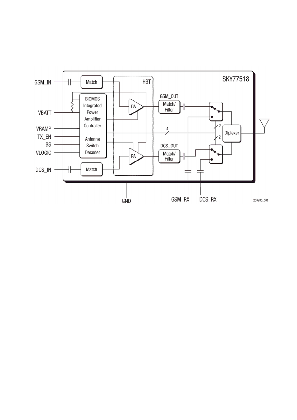
3.2 Power Amplifier Module(SKY77518/ SKY77517)
Figure.3-2-1 SKY77518 FUNCTIONAL BLOCK DIAGRAM
The SKY77518 is a transmit and receive front-end module (FEM) with Integrated Power Amplifier
Control (iPAC™) for dual-band cellular handsets comprising GSM900 and DCS1800 operation.
Designed in a low profile, compact form factor, the SKY77518 offers a complete Transmit VCO-to-
Antenna and Antenna-to-Receive SAW filter solution. The FEM also supports Class 12 General Packet
Radio Service (GPRS) multi-slot operation.
The module consists of a GSM900 PA block and a DCS1800 PA block, impedance-matching circuitry for
50 Ω input and output impedances, TX harmonics filtering, high linearity and low insertion loss PHEMT
RF switches, diplexer and a Power Amplifier Control (PAC) block with internal current sense resistor. A
custom BiCMOS integrated circuit provides the internal PAC function and decoder circuitry to control the
RF switches. The two Heterojunction Bipolar Transistor (HBT) PA blocks are fabricated onto a single
Gallium Arsenide (GaAs) die. One PA block supports the GSM900 band and the other PA block supports
the DCS1800 band. Both PA blocks share common power supply pads to distribute current. The output of
each PA block and the outputs to the two receive pads are connected to the antenna pad through PHEMT RF
switches and a diplexer. The GaAs die, PHEMT die, Silicon (Si) die and passive components are mounted
on a multi-layer laminate substrate. The assembly is encapsulated with plastic overmold. Band selection and
control of transmit and receive modes are performed using two external control pads. Refer to the functional
block diagram in Figure.3-2-1
below. The band select pad (BS) selects between GSM and DCS modes of
19
operation. The transmit enable (TX_EN) pad controls receive or transmit mode of the respective RF switch
(TX = logic 1). Proper timing between transmit enable (TX_EN) and Analog Power Control (VRAMP)
allows for high isolation between the antenna and TXVCO while the VCO is being tuned prior to the
transmit burst.
The SKY77518 is compatible with logic levels from 1.2 V to VCC for BS and TX_EN pads,
depending on the level applied to the VLOGIC pad. This feature provides additional flexibility for the
designer in the selection of FEM interface control logic.
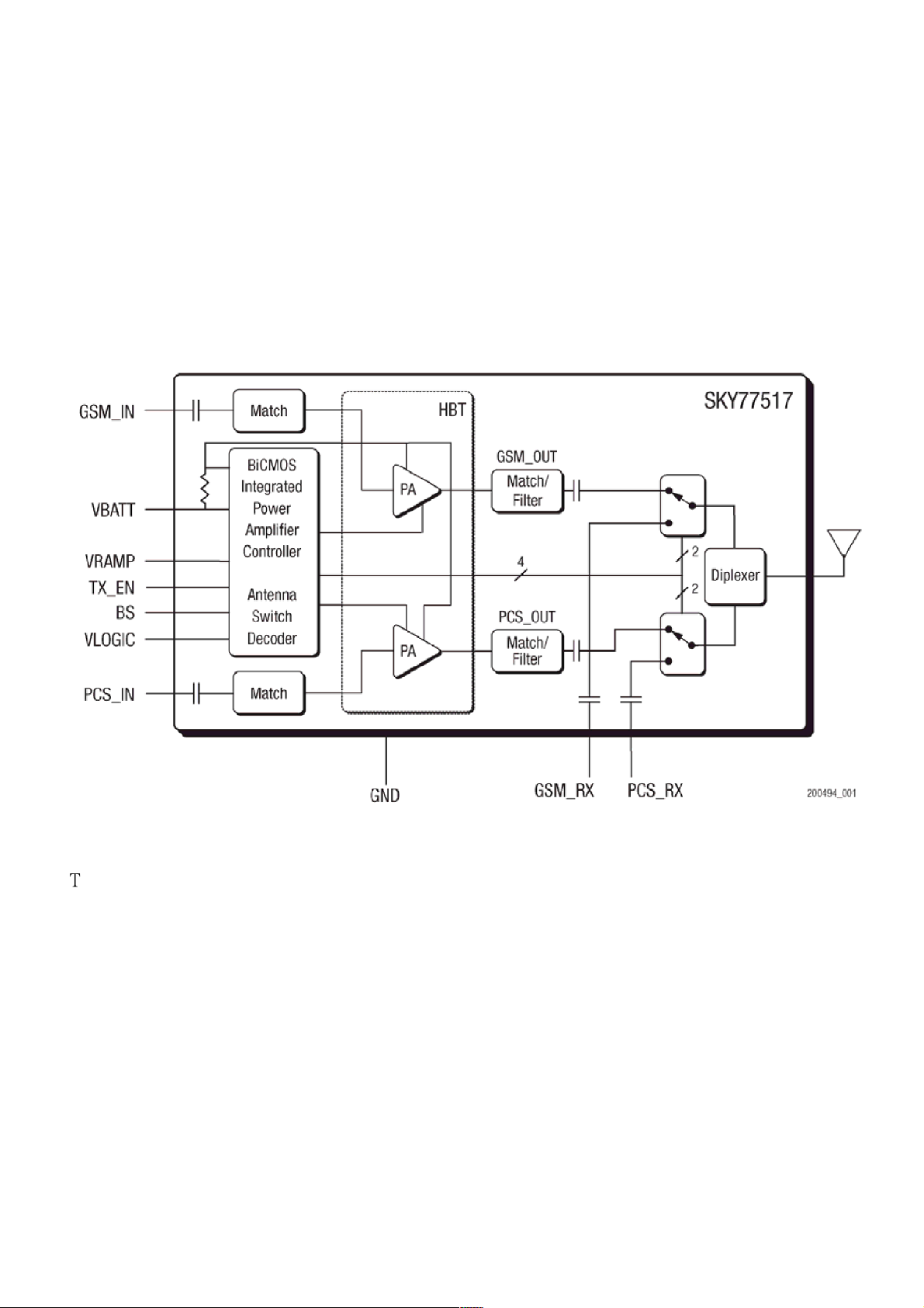
Figure.3-2-2 SKY77517 FUNCTIONAL BLOCK DIAGRAM
The SKY77517–21 is a transmit and receive front-end module (FEM) with Integrated Power Amplifier
Control (iPAC.) for dual-band cellular handsets comprising GSM850 and PCS1900 operation. Designed in a
low profile, compact form factor, the SKY77517–21 offers a complete Transmit VCO-to-Antenna and
Antenna-to-Receive SAW filter solution. The FEM also supports Class 12 General Packet Radio Service
(GPRS) multi-slot operation.
The module consists of a GSM850 PA block and a PCS1900 PA block, impedance-matching
circuitry for 50 Ω input and output impedances, TX harmonics filtering, high linearity and low insertion
loss PHEMT RF switches, diplexer and a Power Amplifier Control (PAC) block with internal current sense
resistor. A custom BiCMOS integrated circuit provides the internal PAC function and decoder circuitry to
control the RF switches. The two Heterojunction Bipolar Transistor (HBT) PA blocks are fabricated onto a
single Gallium Arsenide (GaAs) die. One PA block supports the GSM850 band and the other PA block

20
supports the PCS1900 band. Both PA blocks share common power supply pads to distribute current. The
output of each PA block
and the outputs to the two receive pads are connected to the antenna pad through PHEMT RF switches and a
diplexer. The GaAs die, PHEMT die, Silicon (Si) die and passive components are mounted on a multi-layer
laminate substrate. The assembly is encapsulated with plastic overmold.
Band selection and control of transmit and receive modes are performed using two external control pads.
Refer to the functional block diagram in Figure.3-2-2 below. The band select pad (BS) selects between GSM
and PCS modes of operation. The transmit enable (TX_EN) pad controls receive or transmit mode of the
respective RF switch (TX = logic 1). Proper timing between transmit enable (TX_EN) and Analog Power
Control (VRAMP) allows for high isolation between the antenna and TX-VCO while the VCO is being
tuned prior to the transmit burst.
The SKY77517 is compatible with logic levels from 1.2 V to VCC for BS and TX_EN pads, depending on
the level applied to the VLOGIC pad. This feature provides additional flexibility for the designer in the
selection of FEM interface control logic.
21
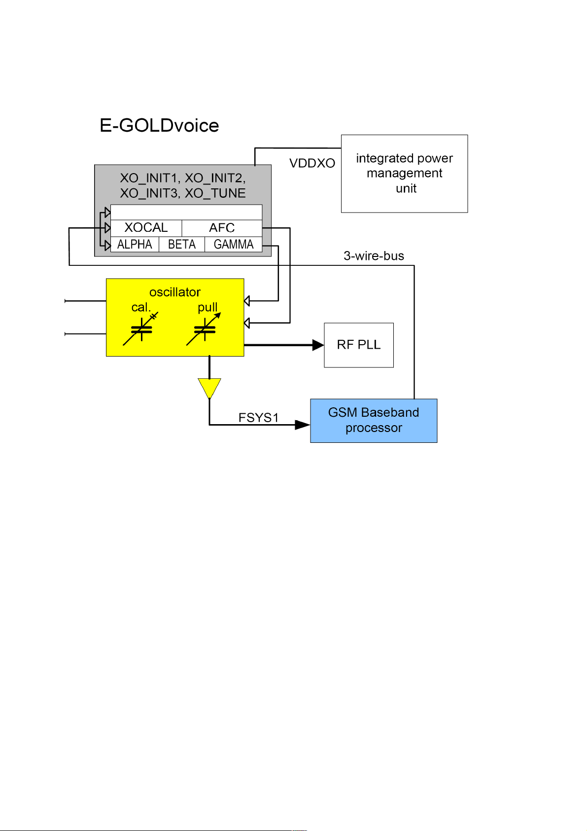
3.3 26MHz Clock (DCXO)
Figure.3
Figure.3----3
Figure.3Figure.3
The XO_TUNE register holds the digital correction value for the crystal oscillator frequency. The
XOMODE bits of XO_INIT1 register contain setup informations for the crystal oscillator (for example,
current programming, etc.).See Figu
The registers XO_INIT2 and XO_INIT3 contain the coefficients information for the linearization unit of
crystal oscillator (LUXO) This linearization unit computes the required digital control word out of the
programmed AFC bits in order to have a linear pulling curve ppm vs. AFC word. The resulting digital
control word DIG is filtered by a digital lowpass filter, which can be scaled or deactivated using the bits
DIGFILT0 and DIGFILT1 of the XO_INIT3 register.
The frequency correction splits into 2 parts:
1. The XOCAL bits in the XO_INIT1 register are used for the coarse frequency adjustment and are set once
for a mobile lifetime (during production test)
2. The XO_TUNE register contains the information for frequency correction when the mobile is used
(correction of temperature drift, crystal aging)
3 Crystal Oscillato
Crystal Oscillator Functional Overview
3 3
Crystal OscillatoCrystal Oscillato
Figure
re .3
FiguFigu
.3----3333 Crystal Oscillator Functional Overview
re re
.3.3
r Functional Overview
r Functional Overviewr Functional Overview
Crystal Oscillator Functional Overview.
Crystal Oscillator Functional Overview Crystal Oscillator Functional Overview
22
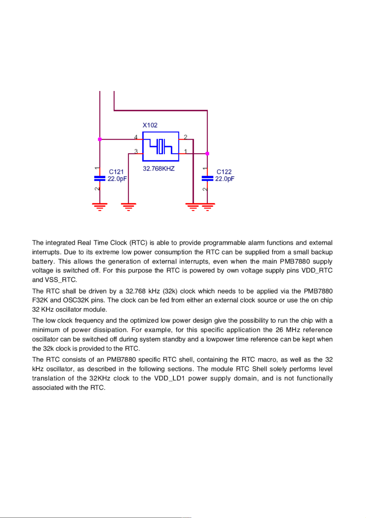
3.4 RTC (32.768KHz Crystal)
Figure.3-4 E-GoldVoice RTC Interface

23
3.5 LCD Interface
Figure.3-5-1 LCD Interface
Figure.3-5-2 Charging PUMP Interface
24
3.6 SIM Card Interface
Figure.3-6 SIM CARD Interface
25
3.7 KEYPAD Interface
Figure.3-7 KEY MAXTRIX Interface
26
3.8 Battery Charging Block Interface
Figure.3-8 Charging IC Interface
27
3.9 RF Interface
Figure.3-9 RF Module/SAW Filter Interface
28
29
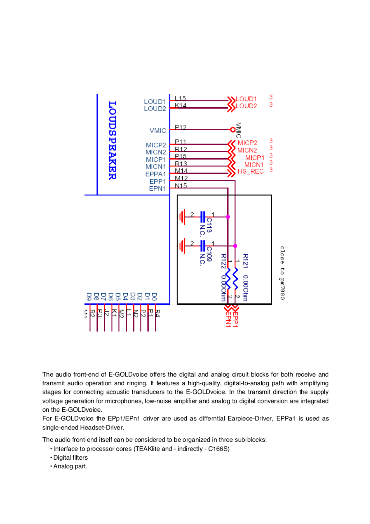
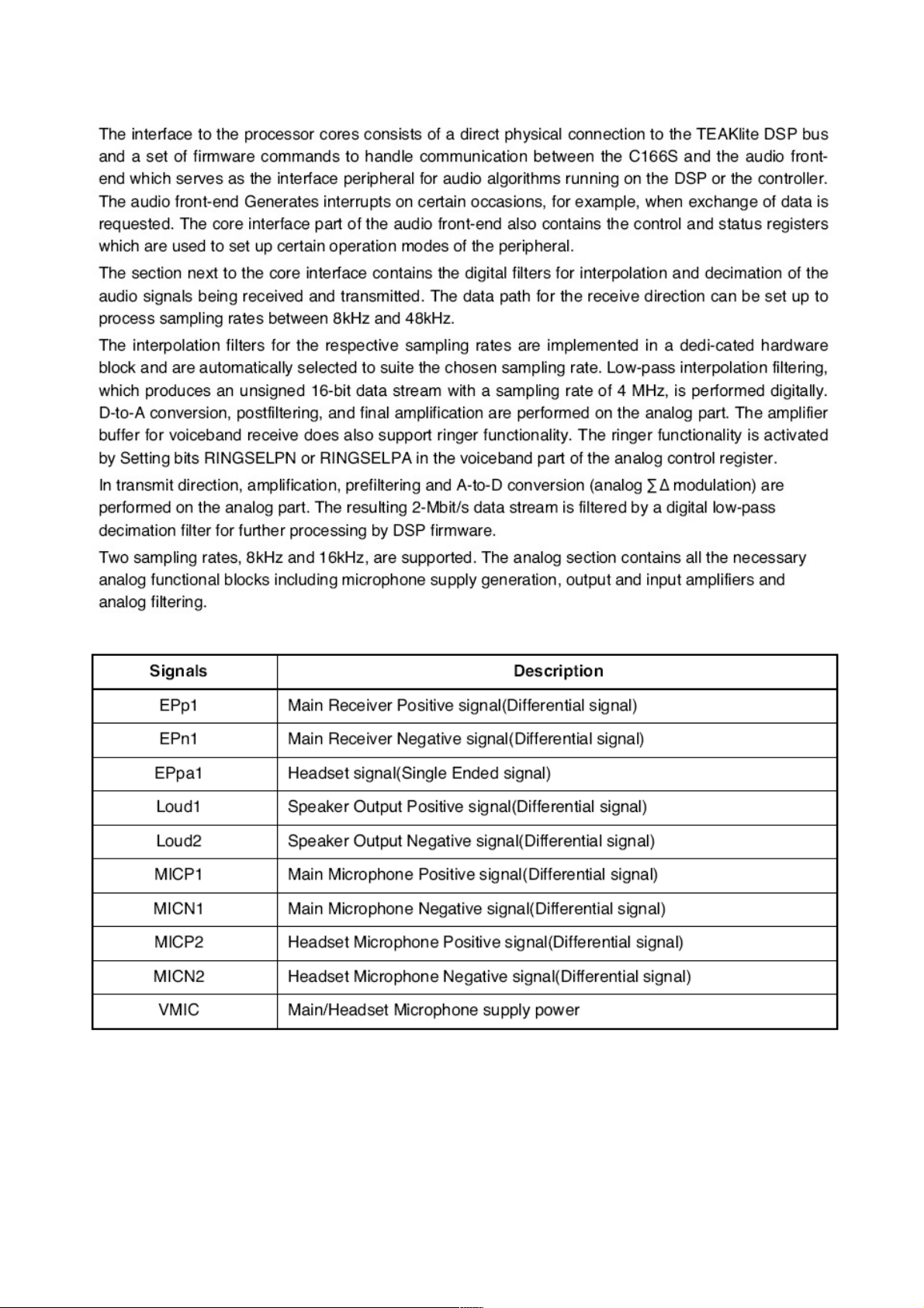
3.10 Audio Interface
Figure.3-10-1 Audio Interface
30
 Loading...