

LG Flatron W2600H Service Manual

COLOR MONITOR
SERVICE MANUAL
Website:http://biz.LGservice.com
CAUTION
BEFORE SERVICING THE UNIT,
READ THE SAFETY PRECAUTIONS IN THIS MANUAL.
CHASSIS NO. : LM83A
MODEL: W2600H(W2600H-PFS.A**QAF)
( ) **Same model for Service
Internal Use Only

- 2 -
CONTENTS
CONTENTS .............................................................................................. 2
PRECAUTION ...........................................................................................3
SPECIFICATION ........................................................................................7
ADJUSTMENT ..........................................................................................9
SERVICE OSD .........................................................................................12
TROUBLE SHOOTING ............................................................................13
BLOCK DIAGRAM...................................................................................17
EXPLODED VIEW ...................................................................................20
REPLACEMENT PARTS LIST ............................................................... 22
SVC. SHEET ........................................................................................... 25
Copyright 2008 LG Electronics. Inc. All right reserved.
Only for training and service purposes
LGE Internal Use Only
- 3 -
PRECAUTION
Copyright 2008 LG Electronics. Inc. All right reserved.
Only for training and service purposes
LGE Internal Use Only
WARNING FOR THE SAFETY-RELATED COMPONENT.
• There are some special components used in LCD
monitor that are important for safety. These parts are
marked on the schematic diagram and the
replacement parts list. It is essential that these critical
parts should be replaced with the manufacturer’s
specified parts to prevent electric shock, fire or other
hazard.
• Do not modify original design without obtaining written
permission from manufacturer or you will void the
original parts and labor guarantee.
TAKE CARE DURING HANDLING THE LCD MODULE
WITH BACKLIGHT UNIT.
• Must mount the module using mounting holes arranged
in four corners.
• Do not press on the panel, edge of the frame strongly
or electric shock as this will result in damage to the
screen.
• Do not scratch or press on the panel with any sharp
objects, such as pencil or pen as this may result in
damage to the panel.
• Protect the module from the ESD as it may damage the
electronic circuit (C-MOS).
• Make certain that treatment person’s body are
grounded through wrist band.
• Do not leave the module in high temperature and in
areas of high humidity for a long time.
• The module not be exposed to the direct sunlight.
• Avoid contact with water as it may a short circuit within
the module.
• If the surface of panel become dirty, please wipe it off
with a softmaterial. (Cleaning with a dirty or rough cloth
may damage the panel.)
WARNING
BE CAREFUL ELECTRIC SHOCK !
• If you want to replace with the new backlight (CCFL) or
inverter circuit, must disconnect the AC adapter
because high voltage appears at inverter circuit about
650Vrms.
• Handle with care wires or connectors of the inverter
circuit. If the wires are pressed cause short and may
burn or take fire.
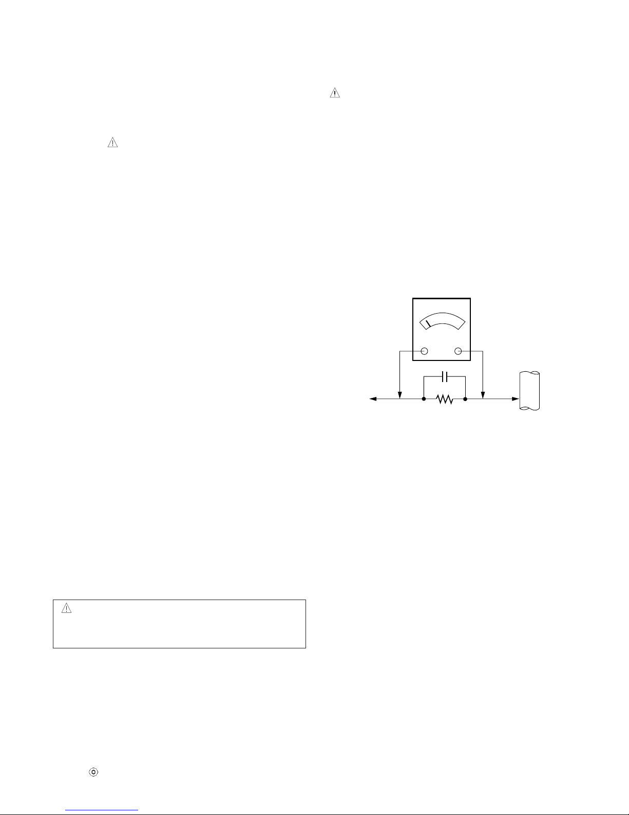
Leakage Current Hot Check Circuit
CAUTION
Please use only a plastic screwdriver to protect yourself
from shock hazard during service operation.
1.5 Kohm/10W
To Instrument's
exposed
METALLIC PARTS
Good Earth Ground
such as WATER PIPE,
CONDUIT etc.
AC Volt-meter

- 4 -
SERVICING PRECAUTIONS
Copyright 2008 LG Electronics. Inc. All right reserved.
Only for training and service purposes
LGE Internal Use Only
CAUTION: Before servicing receivers covered by this
service manual and its supplements and addenda, read
and follow the SAFETY PRECAUTIONS on page 3 of this
publication.
NOTE: If unforeseen circumstances create conflict
between the following servicing precautions and any of the
safety precautions on page 3 of this publication, always
follow the safety precautions. Remember: Safety First.
General Servicing Precautions
1. Always unplug the receiver AC power cord from the AC
power source before;
a. Removing or reinstalling any component, circuit
board module or any other receiver assembly.
b. Disconnecting or reconnecting any receiver electrical
plug or other electrical connection.
c. Connecting a test substitute in parallel with an
electrolytic capacitor in the receiver.
CAUTION: A wrong part substitution or incorrect
polarity installation of electrolytic capacitors may
result in an explosion hazard.
d. Discharging the picture tube anode.
2. Test high voltage only by measuring it with an
appropriate high voltage meter or other voltage
measuring device (DVM, FETVOM, etc) equipped with
a suitable high voltage probe.
Do not test high voltage by "drawing an arc".
3. Discharge the picture tube anode only by (a) first
connecting one end of an insulated clip lead to the
degaussing or kine aquadag grounding system shield
at the point where the picture tube socket ground lead
is connected, and then (b) touch the other end of the
insulated clip lead to the picture tube anode button,
using an insulating handle to avoid personal contact
with high voltage.
4. Do not spray chemicals on or near this receiver or any
of its assemblies.
5. Unless specified otherwise in this service manual,
clean electrical contacts only by applying the following
mixture to the contacts with a pipe cleaner, cottontipped stick or comparable non-abrasive applicator;
10% (by volume) Acetone and 90% (by volume)
isopropyl alcohol (90%-99% strength)
CAUTION: This is a flammable mixture.
Unless specified otherwise in this service manual,
lubrication of contacts in not required.
6. Do not defeat any plug/socket B+ voltage interlocks
with which receivers covered by this service manual
might be equipped.
7. Do not apply AC power to this instrument and/or any of
its electrical assemblies unless all solid-state device
heat sinks are correctly installed.
8. Always connect the test receiver ground lead to the
receiver chassis ground before connecting the test
receiver positive lead.
Always remove the test receiver ground lead last.
9. Use with this receiver only the test fixtures specified in
this service manual.
CAUTION: Do not connect the test fixture ground strap
to any heat sink in this receiver.
Electrostatically Sensitive (ES) Devices
Some semiconductor (solid-state) devices can be
damaged easily by static electricity. Such components
commonly are called Electrostatically Sensitive (ES)
Devices. Examples of typical ES devices are integrated
circuits and some field-effect transistors and
semiconductor "chip" components. The following
techniques should be used to help reduce the incidence of
component damage caused by static by static electricity.
1. Immediately before handling any semiconductor
component or semiconductor-equipped assembly, drain
off any electrostatic charge on your body by touching a
known earth ground. Alternatively, obtain and wear a
commercially available discharging wrist strap device,
which should be removed to prevent potential shock
reasons prior to applying power to the unit under test.
2. After removing an electrical assembly equipped with
ES devices, place the assembly on a conductive
surface such as aluminum foil, to prevent electrostatic
charge buildup or exposure of the assembly.
3. Use only a grounded-tip soldering iron to solder or
unsolder ES devices.
4. Use only an anti-static type solder removal device.
Some solder removal devices not classified as "antistatic" can generate electrical charges sufficient to
damage ES devices.
5. Do not use freon-propelled chemicals. These can
generate electrical charges sufficient to damage ES
devices.
6. Do not remove a replacement ES device from its
protective package until immediately before you are
ready to install it. (Most replacement ES devices are
packaged with leads electrically shorted together by
conductive foam, aluminum foil or comparable
conductive material).
7. Immediately before removing the protective material
from the leads of a replacement ES device, touch the
protective material to the chassis or circuit assembly
into which the device will be installed.
CAUTION: Be sure no power is applied to the chassis
or circuit, and observe all other safety precautions.
8. Minimize bodily motions when handling unpackaged
replacement ES devices. (Otherwise harmless motion
such as the brushing together of your clothes fabric or
the lifting of your foot from a carpeted floor can
generate static electricity sufficient to damage an ES
device.)

- 5 -
Copyright 2008 LG Electronics. Inc. All right reserved.
Only for training and service purposes
LGE Internal Use Only
General Soldering Guidelines
1. Use a grounded-tip, low-wattage soldering iron and
appropriate tip size and shape that will maintain tip
temperature within the range or 500
F to 600 F.
2. Use an appropriate gauge of RMA resin-core solder
composed of 60 parts tin/40 parts lead.
3. Keep the soldering iron tip clean and well tinned.
4. Thoroughly clean the surfaces to be soldered. Use a
mall wire-bristle (0.5 inch, or 1.25cm) brush with a
metal handle.
Do not use freon-propelled spray-on cleaners.
5. Use the following unsoldering technique
a. Allow the soldering iron tip to reach normal
temperature.
(500
F to 600 F)
b. Heat the component lead until the solder melts.
c. Quickly draw the melted solder with an anti-static,
suction-type solder removal device or with solder
braid.
CAUTION: Work quickly to avoid overheating the
circuitboard printed foil.
6. Use the following soldering technique.
a. Allow the soldering iron tip to reach a normal
temperature (500
F to 600 F)
b. First, hold the soldering iron tip and solder the strand
against the component lead until the solder melts.
c. Quickly move the soldering iron tip to the junction of
the component lead and the printed circuit foil, and
hold it there only until the solder flows onto and
around both the component lead and the foil.
CAUTION: Work quickly to avoid overheating the
circuit board printed foil.
d. Closely inspect the solder area and remove any
excess or splashed solder with a small wire-bristle
brush.
IC Remove/Replacement
Some chassis circuit boards have slotted holes (oblong)
through which the IC leads are inserted and then bent flat
against the circuit foil. When holes are the slotted type,
the following technique should be used to remove and
replace the IC. When working with boards using the
familiar round hole, use the standard technique as
outlined in paragraphs 5 and 6 above.
Removal
1. Desolder and straighten each IC lead in one operation
by gently prying up on the lead with the soldering iron
tip as the solder melts.
2. Draw away the melted solder with an anti-static
suction-type solder removal device (or with solder
braid) before removing the IC.
Replacement
1. Carefully insert the replacement IC in the circuit board.
2. Carefully bend each IC lead against the circuit foil pad
and solder it.
3. Clean the soldered areas with a small wire-bristle
brush. (It is not necessary to reapply acrylic coating to
the areas).
"Small-Signal" Discrete Transistor
Removal/Replacement
1. Remove the defective transistor by clipping its leads as
close as possible to the component body.
2. Bend into a "U" shape the end of each of three leads
remaining on the circuit board.
3. Bend into a "U" shape the replacement transistor leads.
4. Connect the replacement transistor leads to the
corresponding leads extending from the circuit board
and crimp the "U" with long nose pliers to insure metal
to metal contact then solder each connection.
Power Output, Transistor Device
Removal/Replacement
1. Heat and remove all solder from around the transistor
leads.
2. Remove the heat sink mounting screw (if so equipped).
3. Carefully remove the transistor from the heat sink of the
circuit board.
4. Insert new transistor in the circuit board.
5. Solder each transistor lead, and clip off excess lead.
6. Replace heat sink.
Diode Removal/Replacement
1. Remove defective diode by clipping its leads as close
as possible to diode body.
2. Bend the two remaining leads perpendicular y to the
circuit board.
3. Observing diode polarity, wrap each lead of the new
diode around the corresponding lead on the circuit
board.
4. Securely crimp each connection and solder it.
5. Inspect (on the circuit board copper side) the solder
joints of the two "original" leads. If they are not shiny,
reheat them and if necessary, apply additional solder.
Fuse and Conventional Resistor
Removal/Replacement
1. Clip each fuse or resistor lead at top of the circuit board
hollow stake.
2. Securely crimp the leads of replacement component
around notch at stake top.
3. Solder the connections.
CAUTION: Maintain original spacing between the
replaced component and adjacent components and the
circuit board to prevent excessive component
temperatures.

- 6 -
Copyright 2008 LG Electronics. Inc. All right reserved.
Only for training and service purposes
LGE Internal Use Only
Circuit Board Foil Repair
Excessive heat applied to the copper foil of any printed
circuit board will weaken the adhesive that bonds the foil
to the circuit board causing the foil to separate from or
"lift-off" the board. The following guidelines and
procedures should be followed whenever this condition is
encountered.
At IC Connections
To repair a defective copper pattern at IC connections use
the following procedure to install a jumper wire on the
copper pattern side of the circuit board. (Use this
technique only on IC connections).
1. Carefully remove the damaged copper pattern with a
sharp knife. (Remove only as much copper as
absolutely necessary).
2. carefully scratch away the solder resist and acrylic
coating (if used) from the end of the remaining copper
pattern.
3. Bend a small "U" in one end of a small gauge jumper
wire and carefully crimp it around the IC pin. Solder the
IC connection.
4. Route the jumper wire along the path of the out-away
copper pattern and let it overlap the previously scraped
end of the good copper pattern. Solder the overlapped
area and clip off any excess jumper wire.
At Other Connections
Use the following technique to repair the defective copper
pattern at connections other than IC Pins. This technique
involves the installation of a jumper wire on the
component side of the circuit board.
1. Remove the defective copper pattern with a sharp
knife.
Remove at least 1/4 inch of copper, to ensure that a
hazardous condition will not exist if the jumper wire
opens.
2. Trace along the copper pattern from both sides of the
pattern break and locate the nearest component that is
directly connected to the affected copper pattern.
3. Connect insulated 20-gauge jumper wire from the lead
of the nearest component on one side of the pattern
break to the lead of the nearest component on the
other side.
Carefully crimp and solder the connections.
CAUTION: Be sure the insulated jumper wire is
dressed so the it does not touch components or sharp
edges.
- 7 -
SPECIFICATIONS
Copyright 2008 LG Electronics. Inc. All right reserved.
Only for training and service purposes
LGE Internal Use Only
1. LCD CHARACTERISTICS
Type : TFT Color LCD Module
Active Display Area : 26 inch (756.228mm) diagonal
Pixel Pitch : 0.2505 (H) x 0.2505 (V)
Color Depth : 16,777,216 colors
Size : 677.30 (H) x 436.80 (V) x 42.30(D)
Electrical Interface : LVDS
Surface Treatment : Anti-Glare, Hard-coating(3H)
Operating Mode : Normally White
Backlight Unit : 4 CCFL
2. OPTICAL CHARACTERISTICS
2-1. Viewing Angle by Contrast Ratio ≥ 5
Left : -80°(Typ) Right : +80°(Typ)
Top :+80°(Typ) Bottom : -80°(Typ)
2-2. Luminance : 180(typ) (Typ.
30) -sRGB
: 200(min), 350(Typ), 400(max)
(Full white pattern, 0.7V)-6500K
: 150(min), 250(Typ), 350(max)
(Full white pattern, 0.7V)-9300K
: 75%(min), 80%(typ)
2-3. Contrast Ratio : 500(Min), 1000(Typ)
DFC->5000:1(Typ)
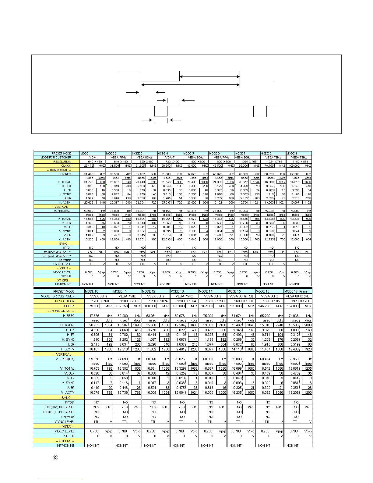
3. SIGNAL (Refer to the Timing Chart)
3-1. Sync Signal
• Type : Separate Sync, SOG, Digital
3-2. Video Input Signal
1) Type : R, G, B Analog
2) Voltage Level : 0~0.71 V
a) Color 0, 0 : 0 Vp-p
b) Color 7, 0 : 0.467Vp-p
c) Color 15, 0 : 0.714Vp-p
3) Input Impedance : 75Ω
3-3. Operating Frequency
Horizontal(Analog) : 30 ~ 83kHz
Horizontal(Digital) : 30 ~ 83kHz
Vertical : 56 ~ 75Hz
4. Max. Resolution
D-sub Analog : 1920 x 1200@60Hz
Digital : 1920 x 1200@60Hz
5. POWER SUPPLY
5-1. Power : AC 100-240V~, 50/60Hz , 0.8A
5-2. Power Consumption
6. ENVIRONMENT
6-1. Operating Temperature : 10°C~35°C (50°F~95°F)
(Ambient)
6-2. Relative Humidity : 10%~80% (Non-condensing)
6-3. MTBF : 50,000 HRS with 90% Confidence
Lamp Life : 50,000 Hours(Min)
7. DIMENSIONS (with TILT/SWIVEL)
Width : 601.9 mm (23.70'')
Depth : 270.2 mm (10.64'')
Height : 463.2 mm (18.24'')
8. WEIGHT (with TILT/SWIVEL)
Net. Weight : 12.3 kg (27.12 lbs)
Gross Weight : 15.4 kg (33.96 lbs)
MODE
POWER ON (NORMAL)
STAND-BY
SUSPEND
DPMS OFF
POWER S/W OFF
H/V SYNC
ON/ON
OFF/ON
ON/OFF
OFF/OFF
-
POWER CONSUMPTION
less than 110W(typ)
130W (USB Full load)
less than 1 W
less than 1 W
less than 1 W
less than 1 W
LED COLOR
BLUE
AMBER
AMBER
AMBER
OFF
VIDEO
ACTIVE
OFF
OFF
OFF
-
- 8 -
TIMING CHART
Copyright 2008 LG Electronics. Inc. All right reserved.
Only for training and service purposes
LGE Internal Use Only
VIDEO
SYNC
B
C
E
A
D
* H/V Timming
- 9 -
LGE Internal Use Only
Copyright
2008 LG Electronics. Inc. All right reserved.
Only for training and service purposes
ADJUSTMENT INSTRUCTION
1. Coverage
Apply to 26" Wide WGC monitor made in Monitor
Factory(Kumi Korea) or made in accordance with the
standard of Kumi Factory process.
2. Appointment
2.1 Adjustment must be done as fixed sequence, and
adjustment sequence can be modified after agreement
with the responsible R&D engineer considering massproduction condition.
2.2 Power : AC100~240 Voltage (Free)
2.3 Input signal : As Product Standard (Signal ROM : ...V1.1)
2.4 Warm-up Time : Over than 30 minutes
2.5 Adjustment equipment : White balance equipment (CA-
210), Display adjust equipment, VG-819 (or VG828),
Oscilloscope, PC (More than 486 computer ) & White
balance adjust program. HDCP Adjusting Jig equipment.
3. Adjustment
3.1 Overview
Use factory automation equipment and adjust automatic
movement. But, do via passivity adjust in error
occurrence.
3.2 Adjustment order(refer to the Adjustment standard and
adjustment command table)
3.2.1 Board Assembly Line
Connect input signal to 15pin D-sub.
Ready for adjustment : check whether adjustment
command works normally or not and the operating
state of each mode.
Check the display state of gray color when 256 gray
scale pattern is embodied.
Read by EEPROM Read Command to check
whether initial value is correct or not.
3.2.2 Total Assembly Line
Input analog signal.
(1920x1200@60Hz, Model #127)
Write HDCP Key to EEPROM(24C16) by using
DDC2AB protocol & HDCP Adjusting Jig equipment
[Address 0xAC 80, 292 bytes]
If error is occurred, write and check again.
Send Adjust Command [E6 00] to Refresh HDCP
Function.
Ready : Heat-run during 30 minutes in the state with
signal
Connect input signal to D-sub.
Default value before adjustment : Contrast "70" ,
Brightness "100(Max)"
3.2.3 Adjustment of Horizontal/Verticality screen position,
Clock and Clock Phase at each Mode.
There is no special factory mode adjustment.
Writing initial value of EEPROM in Board Assembly
line is adjusting Preset Mode and Reset mode.
(EEPROM is initialized when AC Power is ON first.)
If the change of FOS data is needed after M.P, it is
possible by writing Mode Data with EEPROM write
command or modifying the Mode Data in MICOM
itself.
# Caution) Must keep power-on more than 3
seconds after AC Power-on first time.
3.2.4 Color coordinates adjustment and Luminance
adjustment.
3.2.4.1 Color coordinates adjustment
Monitor Contrast / Brightness
- Contrast : 70
- Brightness : 100(Max)
CA-210 : Channel 13 (For WCG Monitor)
Signal Generator : At cut-off and drive ‡ 16 step
pattern for ADC
- Output Voltage : 700 mVp-p
- Output Mode : Mode 127(WUXGA 60Hz)
mode Setting.
3.2.4.2 Adjustment : Board Assembly Line.
Input 16 step pattern for ADC (Mode127, pattern
29). (Video level : 700 mVp-p)
Adjust by commanding AUTO_COLOR_ADJUST
Confirm "Success" message in Screen or Check
the data of 0XC0, 0XC1 address of
EEPROM(0xAA) is 0xAA after waiting 5 seconds.
If there is "FAULT" message or the data of 0xCO,
0xC1 address of EEPROM(0xAA) is not 0xAA, do
adjust again.
If all Adjustment is completed, the values of
6500K, User Color and 9300K are saved
automatically.
3.2.4.3 Confirm at Total Assembly Line : adjustment.
Check the data of 0xC0, 0xC1 address of
EEPROM(0xAA) is 0xAA.
If the data of 0XC0, C1 address of
EEPROM(0xAA) is not 0xAA, do adjust again by
3.2.4.2.
3.2.4.4 Confirm PRESET 6500K Color coordinates and
Confirm PRESET 9300K Color coordinates .
Set as Aging mode ON, by commanding
AGING_ON/OFF command code.
Select Module that is being used in present
production by commanding MODULE SELECT.
Send SYSTEM RESET command to set Module
data.
Input Full White Pattern (Video level : 700 mVp-p).
Set as 9300K by commanding
COLOR_MODE_CHANGE Command code.
Confirm to meet x = 0.283 0.03, y=0.298 0.03
Save 9300K Color by commanding COLOR SAVE
Command code.
Input Full White Pattern (Video level : 700 mVp-p)
Set as 6500K by commanding
COLOR_MODE_CHANGE Command code.
Confirm to meet x = 0.313 0.03, y=0.329 0.03
Set as sRGB by commanding
COLOR_MODE_CHANGE Command code.
Adjust to meet Y = 180 50, and confirm.
- 10 -
Copyright 2008 LG Electronics. Inc. All right reserved.
Only for training and service purposes
LGE Internal Use Only
3.2.4.5 Confirm User color coordinates .
Confirm Whether User color is saved same as
6500K.
After confirming Color coordinates, Must return to
6500K
Confirm whether user color is 50. If the value of
user color(R/G/B) is 30, do adjust again by
3.2.4.2.
3.2.5 Confirm Operation state.
3.2.5.1 Operation mode : Confirm whether each appointed
mode operate correctly or not
3.2.5.2 Confirmation of Adjustment condition and
operation : Confirm whether it meet Auto/Manual
equipement Adjustment standard or not.
Confirm Analog screen state : Confirm screen
state at below mode.
Appointment mode : 640*480 @60Hz (Mode 2),
800*600@75Hz(Mode 5)
1024*768@60Hz(Mode 6),
1280*1024@60Hz(Mode 9),
1680*1050@60Hz(Mode 12), 1920*1200@60Hz
SMPTE pattern(Check 0%,5%,95%,100%)-Mode
can be added.
Check HDCP signal screen by using Video
generator that generate HDCP signal
3.2.5.3 Confirm Auto adjustment operation.
Input Analog 1 line on/off & Rectangle Pattern at
Mode 10(1920x1200@60Hz)
Confirm adjustment operation by changing Clock,
Phase,H/V Position.
Check Clock, Phase by pressing AUTO Key.
Confirm first set of new lot by periods
3.2.5.4 Other quality
Confirm that each items satisfy under standard
condition that was written product spec.
Confirm Applying Module & MICOM Setting ‡
Confirm with Service OSD
-> Confirm at Service OSD by "Menu + Power key"
on .(from Power off)
-> Confirm first set of new lot by periods, and
confirm periodically when there is Process
change or Adjustment setting change.
3.2.5.5 OSD & Adjustment device Confirmation : Confirm
operation mentioned as product spec.
Vary Brightness and Contrast and confirm the
variation of Luminance and display status.
Operate the f.engine function and confirm
variation of Luminance.
Make sure to do FACTORY RESET after
confirmation of OSD function.
3.2.5.6 Confirm the display state by inputting 8 color Bar
Pattern & 256 Gray Scale pattern
3.2.5.7. DPM operation confirmation : Check if Power LED
Color and Power Consumption operates as
standard.
Measurement Condition : 230V@ 50Hz (Analog)
Confirm DPM operation at the state of screen
without Video Signal.(refer to Spec at Page 11)
3.2.5.8 DDC EDID Write
- Digital part EDID data
Confirm whether module selection is correct or not
on the self-diagnostics OSD with signal cable
disconnected.
Connect Digital Signal Cable to DVI-D wafer.
Write EDID DATA to EEPROM(24C02) by using
DDC2B protocol.
Check whether written EDID data is correct or not.
(refer to Product spec).- Analog part EDID data
Connect analog Signal Cable to D-sub wafer.
Write EDID DATA to EEPROM(24C02) by using
DDC2B protocol.
Check whether written EDID data is correct or not.
(refer to Product spec).
-> After writing EDID, send Elapsed Time Clear
command. (Elapsed time should not be
displayed, after EDID writing)
: Confirm periodically (in the first set of new lot,
process change) whether module name and
aging time disappeared on the self-diagnostics
OSD with signal cable disconnected.
-> If Elapsed Time Clear command isn’t executed,
module name, aging time and TCO word appear
on the self-diagnostics OSD.(Module name and
aging time should not appear after writing EDID)
-> Make sure to do FACTORY RESET at the final
process.
3.2.5.9. Shipping condition
Contrast : 70
Power Switch : Off
Brightness : 100(Max)
Color Select : Preset (6500K)
Language Select : Refer to product spec
OSD Position : Center
Power indicator : ON
Flatron f-engine : Normal
3.2.6 USB 2.0 Check
To check USB 2.0 High-Speed, We need a PC which
has CATC Test program.
Connect ups-tream to Monitor and PC
Connect down-stream to Monitor and PC.
Run CATC Program and Check OK or not
 Loading...