

Page 1
COLOR MONITOR
SERVICE MANUAL
Website:http://biz.LGservice.com
E-mail:http://www.LGEservice.com/techsup.html
CAUTION
BEFORE SERVICING THE UNIT,
READ THE SAFETY PRECAUTIONS IN THIS MANUAL.
MENU SELECT
Brightview
MODEL:
T710BH
(T710BHL-AL**E)
CHASSIS NO. : CA-136
T710SH
(T710BHL-AL**M)
Issue Date; 2004. 7.
T710B
T710S
(T710BL-AL**E)
(T710BL-AL**M)
Page 2
1. PICTURE TUBE
Size : 17 inch
DefIection Angle : 90¡
Neck Diameter : 29.1 mm
Stripe Pitch : 0.25 mm
Face Treatment : W-ARASC (Anti-Reflection and
Anti-Static Coating)
Internal : Anti-Glare
2. SIGNAL
2-1. Horizontal & Vertical Sync
1) Input Voltage Level : Low=0~1.2V, High=2.5~5.5V
2) Sync Polarity : Positive or Negative
2-2. Video Input Signal
1) Voltage Level : 0 ~ 0.7 Vp-p
a) Color 0, 0 : 0 Vp-p
b) Color 7, 0 : 0.467 Vp-p
c) Color 15, 0 : 0.7 Vp-p
2) Input Impedance : 75
3) Video Color : R, G, B Analog
4) Signal Format : Refer to the Timing Chart
2-3. Signal Connector
3 row 15-pin Connector (Attached)
2-4. Scanning Frequency
Horizontal : 30 ~ 71 kHz
Vertical : 50 ~ 160 Hz
3. POWER SUPPLY
3-1. Power Range
AC 100-240V~ 50/ 60Hz, 1.0A
3-2. Power Consumption
4. DISPLAY AREA
4-1. Active Video Area :
¥ Max Image Size - 325.1 x 243.8 mm (12.80" x 9.60")
¥ Preset Image Size - 310 x 230 mm (12.20" x 9.06")
4-2. Display Color : Full Colors
4-3. Display Resolution : 1280 x 1024 / 60Hz(Max)
(Non-Interlace)
4-4. Video Bandwidth : 110 MHz
5. ENVIRONMENT
5-1. Operating Temperature: 0¡C ~ 40¡C
(Ambient)
5-2. Relative Humidity : 10%~ 80%
(Non-condensing)
5-3. Altitude : 5,000 m
6. DIMENSIONS (with TILT/SWIVEL)
Width : 400 mm (15.75 inch)
Depth : 411 mm (16.18 inch)
Height : 401 mm (15.79 inch)
7. WEIGHT (with TILT/SWIVEL)
Net Weight : 15.1 kg (33.96 lbs.)
Gross Weight : 18.1 kg (39.67 lbs.)
CONTENTS
- 2 -
SPECIFICATIONS ................................................... 2
SAFETY PRECAUTIONS ........................................ 3
TIMING CHART ....................................................... 7
WIRING DIAGRAM ................................................. 8
DISASSEMBLY ....................................................... 9
BLOCK DIAGRAM ...................................................
10
DESCRIPTION OF BLOCK DIAGRAM................... 11
ADJUSTMENT ....................................................... 12
TROUBLESHOOTING GUIDE .............................. 13
EXPLODED VIEW...................................................34
REPLACEMENT PARTS LIST ............................... 36
SCHEMATIC DIAGRAM......................................... 42
PRINTED CIRCUIT BOARD................................... 44
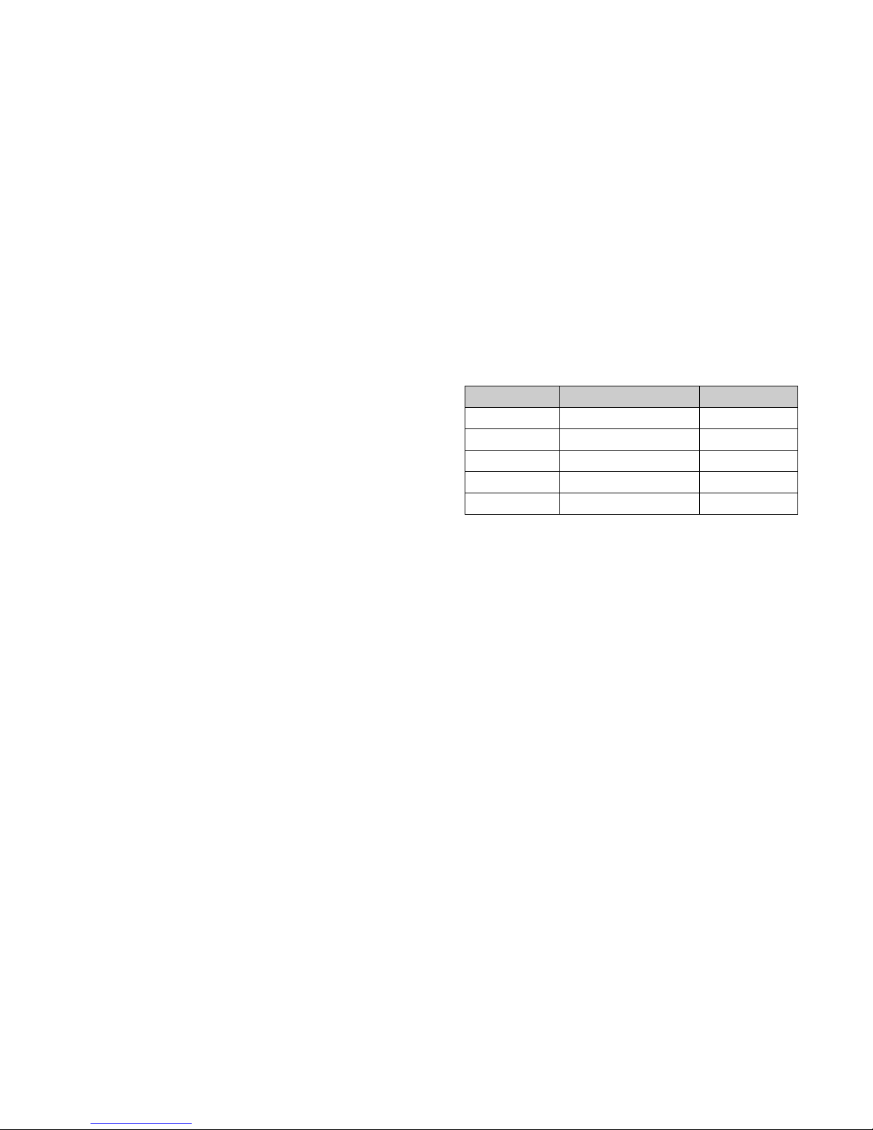
SPECIFICATIONS
MODE
MAX
NORMAL (ON)
STAND-BY
SUSPEND
DPMS OFF
POWER CONSUMPTION
85 W
73 W
less than 15 W
less than 15 W
less than 5 W
LED COLOR
GREEN
GREEN
FLASH
FLASH
FLASH
SERVICE PRECAUTION.......................................... 4
Page 3
SAFETY PRECAUTIONS
- 3 -
SAFETY-RELATED COMPONENT WARNING!
There are special components used in this color monitor
which are important for safety. These parts are marked
on the schematic diagram and the replacement
parts list. It is essential that these critical parts should be
replaced with the manufacturer's specified parts to prevent
X-radiation, shock, fire, or other hazards. Do not modify
the original design without obtaining written permission
from manufacturer or you will void the original parts and
labor guarantee.
CAUTION:
No modification of any circuit should be
attempted.
Service work should be performed only after
you are thoroughly familiar with all of the
following safety checks and servicing
guidelines.
SAFETY CHECK
Care should be taken while servicing this color monitor
because of the high voltage used in the deflection circuits.
These voltages are exposed in such areas as the
associated flyback and yoke circuits.
FIRE & SHOCK HAZARD
An isolation transformer must be inserted between the
color monitor and AC power line before servicing the
chassis.
• In servicing, attention must be paid to the original lead
dress specially in the high voltage circuit. If a short
circuit is found, replace all parts which have been
overheated as a result of the short circuit.
• All the protective devices must be reinstalled per the
original design.
• Soldering must be inspected for the cold solder joints,
frayed leads, damaged insulation, solder splashes, or
the sharp points. Be sure to remove all foreign
materials.
IMPLOSION PROTECTION
All used display tubes are equipped with an integral
implosion protection system, but care should be taken to
avoid damage and scratching during installation. Use only
same type display tubes.
X-RADIATION
The only potential source of X-radiation is the picture tube.
However, when the high voltage circuitry is operating
properly there is no possibility of an X-radiation problem.
The basic precaution which must be exercised is keep the
high voltage at the factory recommended level; the normal
high voltage is about 25.8kV. The following steps describe
how to measure the high voltage and how to prevent Xradiation.
Note : It is important to use an accurate high voltage
meter calibrated periodically.
• To measure the high voltage, use a high impedance
high voltage meter, connect (–) to chassis and (+) to
the CDT anode cap.
• Set the brightness control to maximum point at full
white pattern.
• Measure the high voltage. The high voltage meter
should be indicated at the factory recommended level.
• If the meter indication exceeds the maximum level,
immediate service is required to prevent the possibility
of premature component failure.
• To prevent X-radiation possibility, it is essential to use
the specified picture tube.
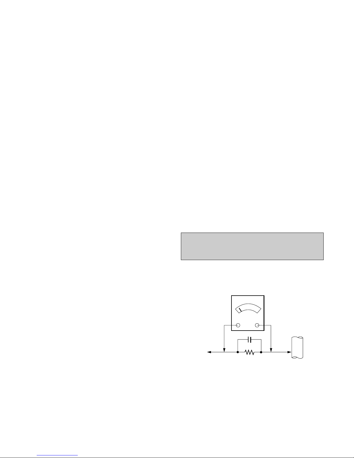
Leakage Current Hot Check Circuit
CAUTION:
Please use only a plastic screwdriver to protect yourself
from shock hazard during service operation.
1.5 Kohm/10W
To Instrument's
exposed
METALLIC PARTS
Good Earth Ground
such as WATER PIPE,
CONDUIT etc.
AC Volt-meter
Page 4

- 4 -
SERVICING PRECAUTIONS
CAUTION: Before servicing receivers covered by this
service manual and its supplements and addenda, read
and follow the SAFETY PRECAUTIONS on page 3 of this
publication.
NOTE: If unforeseen circumstances create conflict
between the following servicing precautions and any of the
safety precautions on page 3 of this publication, always
follow the safety precautions. Remember: Safety First.
General Servicing Precautions
1. Always unplug the receiver AC power cord from the AC
power source before;
a. Removing or reinstalling any component, circuit
board module or any other receiver assembly.
b. Disconnecting or reconnecting any receiver electrical
plug or other electrical connection.
c. Connecting a test substitute in parallel with an
electrolytic capacitor in the receiver.
CAUTION: A wrong part substitution or incorrect
polarity installation of electrolytic capacitors may
result in an explosion hazard.
d. Discharging the picture tube anode.
2. Test high voltage only by measuring it with an
appropriate high voltage meter or other voltage
measuring device (DVM, FETVOM, etc) equipped with
a suitable high voltage probe.
Do not test high voltage by "drawing an arc".
3. Discharge the picture tube anode only by (a) first
connecting one end of an insulated clip lead to the
degaussing or kine aquadag grounding system shield
at the point where the picture tube socket ground lead
is connected, and then (b) touch the other end of the
insulated clip lead to the picture tube anode button,
using an insulating handle to avoid personal contact
with high voltage.
4. Do not spray chemicals on or near this receiver or any
of its assemblies.
5. Unless specified otherwise in this service manual,
clean electrical contacts only by applying the following
mixture to the contacts with a pipe cleaner, cottontipped stick or comparable non-abrasive applicator;
10% (by volume) Acetone and 90% (by volume)
isopropyl alcohol (90%-99% strength)
CAUTION: This is a flammable mixture.
Unless specified otherwise in this service manual,
lubrication of contacts in not required.
6. Do not defeat any plug/socket B+ voltage interlocks
with which receivers covered by this service manual
might be equipped.
7. Do not apply AC power to this instrument and/or any of
its electrical assemblies unless all solid-state device
heat sinks are correctly installed.
8. Always connect the test receiver ground lead to the
receiver chassis ground before connecting the test
receiver positive lead.
Always remove the test receiver ground lead last.
9. Use with this receiver only the test fixtures specified in
this service manual.
CAUTION: Do not connect the test fixture ground strap
to any heat sink in this receiver.
Electrostatically Sensitive (ES) Devices
Some semiconductor (solid-state) devices can be
damaged easily by static electricity. Such components
commonly are called Electrostatically Sensitive (ES)
Devices. Examples of typical ES devices are integrated
circuits and some field-effect transistors and
semiconductor "chip" components. The following
techniques should be used to help reduce the incidence of
component damage caused by static by static electricity.
1. Immediately before handling any semiconductor
component or semiconductor-equipped assembly, drain
off any electrostatic charge on your body by touching a
known earth ground. Alternatively, obtain and wear a
commercially available discharging wrist strap device,
which should be removed to prevent potential shock
reasons prior to applying power to the unit under test.
2. After removing an electrical assembly equipped with
ES devices, place the assembly on a conductive
surface such as aluminum foil, to prevent electrostatic
charge buildup or exposure of the assembly.
3. Use only a grounded-tip soldering iron to solder or
unsolder ES devices.
4. Use only an anti-static type solder removal device.
Some solder removal devices not classified as "antistatic" can generate electrical charges sufficient to
damage ES devices.
5. Do not use freon-propelled chemicals. These can
generate electrical charges sufficient to damage ES
devices.
6. Do not remove a replacement ES device from its
protective package until immediately before you are
ready to install it. (Most replacement ES devices are
packaged with leads electrically shorted together by
conductive foam, aluminum foil or comparable
conductive material).
7. Immediately before removing the protective material
from the leads of a replacement ES device, touch the
protective material to the chassis or circuit assembly
into which the device will be installed.
CAUTION: Be sure no power is applied to the chassis
or circuit, and observe all other safety precautions.
8. Minimize bodily motions when handling unpackaged
replacement ES devices. (Otherwise harmless motion
such as the brushing together of your clothes fabric or
the lifting of your foot from a carpeted floor can
generate static electricity sufficient to damage an ES
device.)
Page 5

- 5 -
General Soldering Guidelines
1. Use a grounded-tip, low-wattage soldering iron and
appropriate tip size and shape that will maintain tip
temperature within the range or 500
F to 600 F.
2. Use an appropriate gauge of RMA resin-core solder
composed of 60 parts tin/40 parts lead.
3. Keep the soldering iron tip clean and well tinned.
4. Thoroughly clean the surfaces to be soldered. Use a
mall wire-bristle (0.5 inch, or 1.25cm) brush with a
metal handle.
Do not use freon-propelled spray-on cleaners.
5. Use the following unsoldering technique
a. Allow the soldering iron tip to reach normal
temperature.
(500
F to 600 F)
b. Heat the component lead until the solder melts.
c. Quickly draw the melted solder with an anti-static,
suction-type solder removal device or with solder
braid.
CAUTION: Work quickly to avoid overheating the
circuitboard printed foil.
6. Use the following soldering technique.
a. Allow the soldering iron tip to reach a normal
temperature (500
F to 600 F)
b. First, hold the soldering iron tip and solder the strand
against the component lead until the solder melts.
c. Quickly move the soldering iron tip to the junction of
the component lead and the printed circuit foil, and
hold it there only until the solder flows onto and
around both the component lead and the foil.
CAUTION: Work quickly to avoid overheating the
circuit board printed foil.
d. Closely inspect the solder area and remove any
excess or splashed solder with a small wire-bristle
brush.
IC Remove/Replacement
Some chassis circuit boards have slotted holes (oblong)
through which the IC leads are inserted and then bent flat
against the circuit foil. When holes are the slotted type,
the following technique should be used to remove and
replace the IC. When working with boards using the
familiar round hole, use the standard technique as
outlined in paragraphs 5 and 6 above.
Removal
1. Desolder and straighten each IC lead in one operation
by gently prying up on the lead with the soldering iron
tip as the solder melts.
2. Draw away the melted solder with an anti-static
suction-type solder removal device (or with solder
braid) before removing the IC.
Replacement
1. Carefully insert the replacement IC in the circuit board.
2. Carefully bend each IC lead against the circuit foil pad
and solder it.
3. Clean the soldered areas with a small wire-bristle
brush. (It is not necessary to reapply acrylic coating to
the areas).
"Small-Signal" Discrete Transistor
Removal/Replacement
1. Remove the defective transistor by clipping its leads as
close as possible to the component body.
2. Bend into a "U" shape the end of each of three leads
remaining on the circuit board.
3. Bend into a "U" shape the replacement transistor leads.
4. Connect the replacement transistor leads to the
corresponding leads extending from the circuit board
and crimp the "U" with long nose pliers to insure metal
to metal contact then solder each connection.
Power Output, Transistor Device
Removal/Replacement
1. Heat and remove all solder from around the transistor
leads.
2. Remove the heat sink mounting screw (if so equipped).
3. Carefully remove the transistor from the heat sink of the
circuit board.
4. Insert new transistor in the circuit board.
5. Solder each transistor lead, and clip off excess lead.
6. Replace heat sink.
Diode Removal/Replacement
1. Remove defective diode by clipping its leads as close
as possible to diode body.
2. Bend the two remaining leads perpendicular y to the
circuit board.
3. Observing diode polarity, wrap each lead of the new
diode around the corresponding lead on the circuit
board.
4. Securely crimp each connection and solder it.
5. Inspect (on the circuit board copper side) the solder
joints of the two "original" leads. If they are not shiny,
reheat them and if necessary, apply additional solder.
Fuse and Conventional Resistor
Removal/Replacement
1. Clip each fuse or resistor lead at top of the circuit board
hollow stake.
2. Securely crimp the leads of replacement component
around notch at stake top.
3. Solder the connections.
CAUTION: Maintain original spacing between the
replaced component and adjacent components and the
circuit board to prevent excessive component
temperatures.
Page 6

- 6 -
Circuit Board Foil Repair
Excessive heat applied to the copper foil of any printed
circuit board will weaken the adhesive that bonds the foil
to the circuit board causing the foil to separate from or
"lift-off" the board. The following guidelines and
procedures should be followed whenever this condition is
encountered.
At IC Connections
To repair a defective copper pattern at IC connections use
the following procedure to install a jumper wire on the
copper pattern side of the circuit board. (Use this
technique only on IC connections).
1. Carefully remove the damaged copper pattern with a
sharp knife. (Remove only as much copper as
absolutely necessary).
2. carefully scratch away the solder resist and acrylic
coating (if used) from the end of the remaining copper
pattern.
3. Bend a small "U" in one end of a small gauge jumper
wire and carefully crimp it around the IC pin. Solder the
IC connection.
4. Route the jumper wire along the path of the out-away
copper pattern and let it overlap the previously scraped
end of the good copper pattern. Solder the overlapped
area and clip off any excess jumper wire.
At Other Connections
Use the following technique to repair the defective copper
pattern at connections other than IC Pins. This technique
involves the installation of a jumper wire on the
component side of the circuit board.
1. Remove the defective copper pattern with a sharp
knife.
Remove at least 1/4 inch of copper, to ensure that a
hazardous condition will not exist if the jumper wire
opens.
2. Trace along the copper pattern from both sides of the
pattern break and locate the nearest component that is
directly connected to the affected copper pattern.
3. Connect insulated 20-gauge jumper wire from the lead
of the nearest component on one side of the pattern
break to the lead of the nearest component on the
other side.
Carefully crimp and solder the connections.
CAUTION: Be sure the insulated jumper wire is
dressed so the it does not touch components or sharp
edges.
Page 7
- 7 -
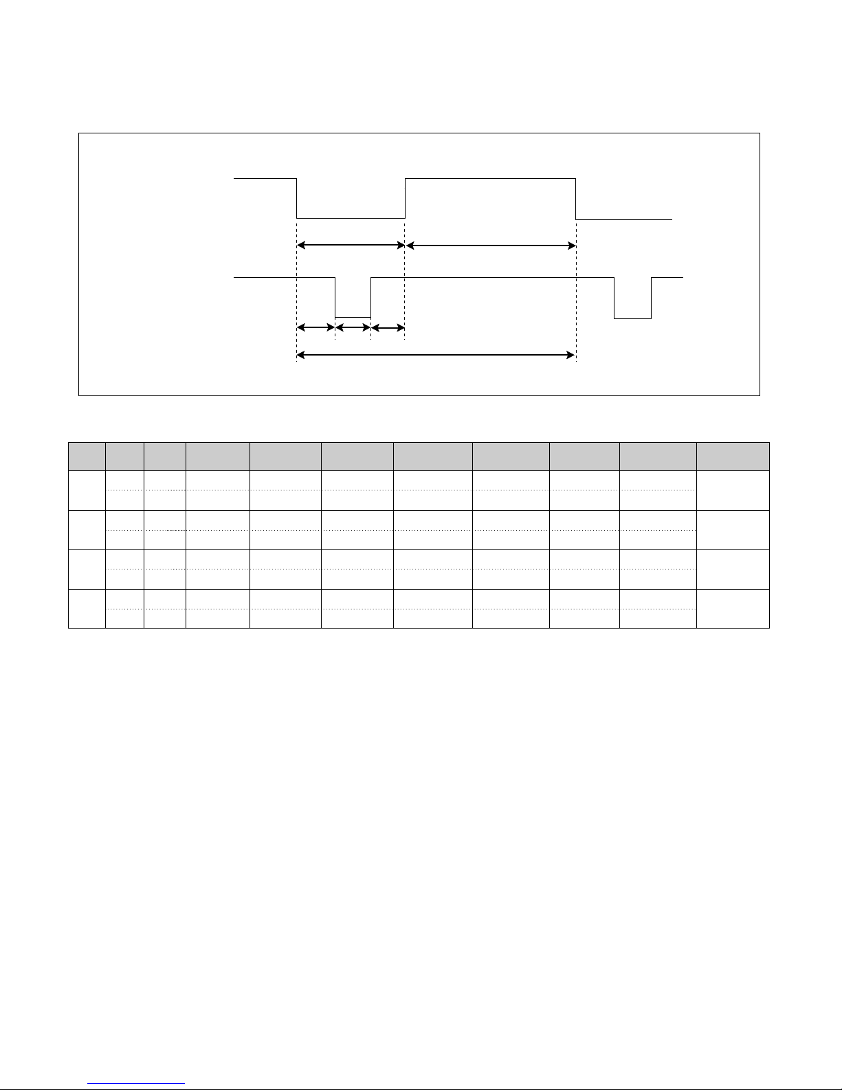
TIMING CHART
VIDEO
SYNC
C
E
D
F
A
B
* No Composite Mode.
H – 37.50 26.67 20.32 6.35 2.03 3.81 0.51
V – 74.99 13.335 12.802 0.533 0.080 0.427 0.026
H + 46.88 21.33 16.16 5.17 1.62 3.23 0.32
V + 75.01 13.331 12.798 0.533 0.064 0.448 0.021
H + 53.68 18.63 14.22 4.41 1.14 2.70 0.57
V + 85.07 11.755 11.178 0.577 0.056 0.503 0.018
H + 68.677 14.561 10.836 3.725 1.016 2.201 0.508
V + 85.00 11.764 11.182 0.582 0.044 0.524 0.014
Mode
H/V
Sort
1
2
3
4
640x480
75Hz
800x600
85Hz
1024x768
85Hz
800x600
75Hz
<< Dot Clock (MHz), Horizontal Frequency (kHz), Vertical Frequency (Hz), Horizontal etc... (µs), Vertical etc... (ms) >>
Sync
Polarity
Frequency
Total Period
(A)
Video Active
Time (B)
Sync Duration
(E)
Blanking Time
(C)
Back Porch
(F)
Front Porch
(D)
Resolution
Page 8
- 8 -
DISASSEMBLY
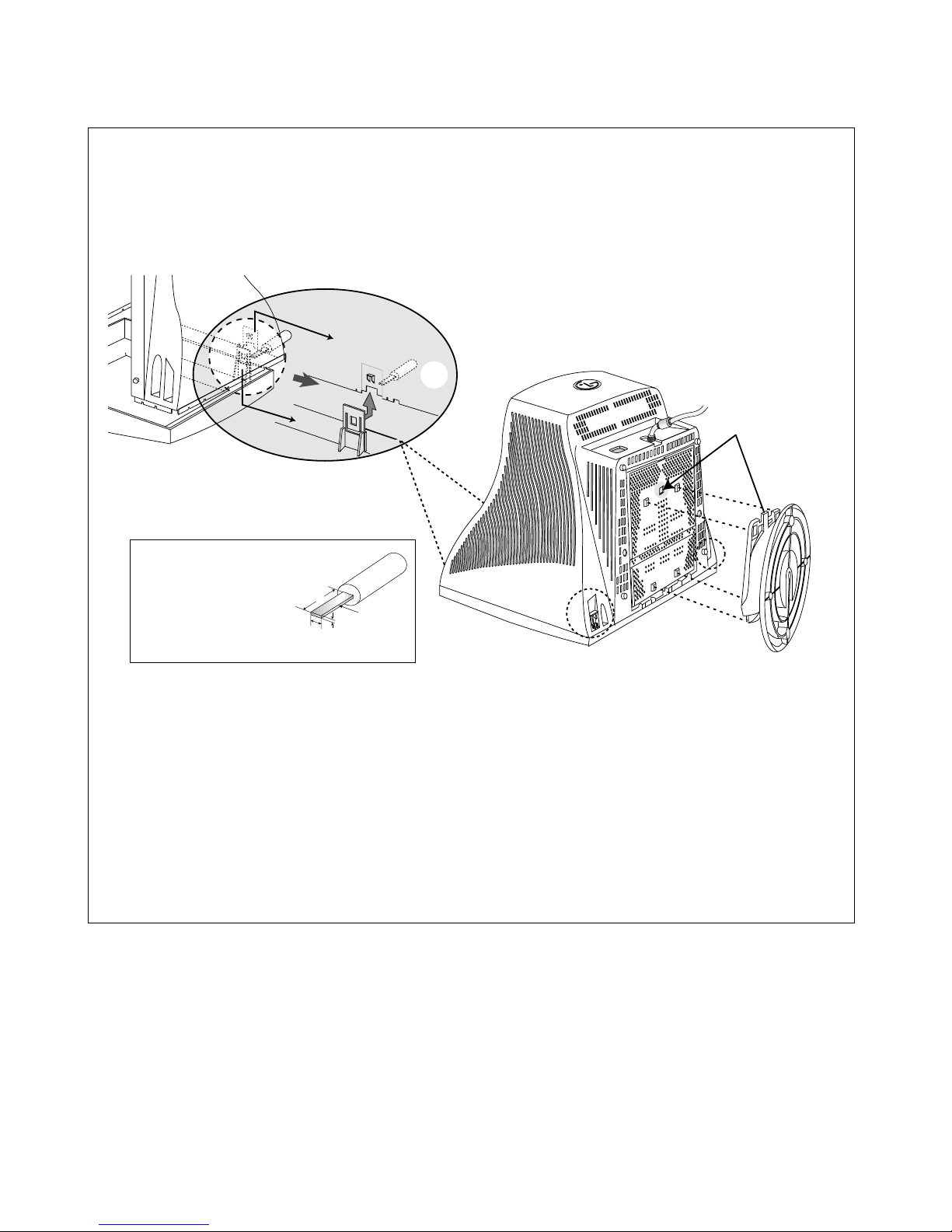
1. TILT/SWIVEL & BACK COVER REMOVAL
1) Set the monitor face downward.
2) Carefully remove the Tilt/Swivel by pulling it upward.
3) Pressing the latch (b), Back cover by pushing it upward.
4) Release the latch (c). (See Tip Spec.)
5) Slide the Back Cover away from the Front Cabinet of the monitor.
Tip Spec.
A(Width) : 5.0~15.0mm
B(Depth) : 0.6~0.9mm
C(Height) : 12.0mm
Back Cover
(c)
Cabinet
(a)
C
Tip
B
A
Page 9
WIRING DIAGRAM
- 9 -
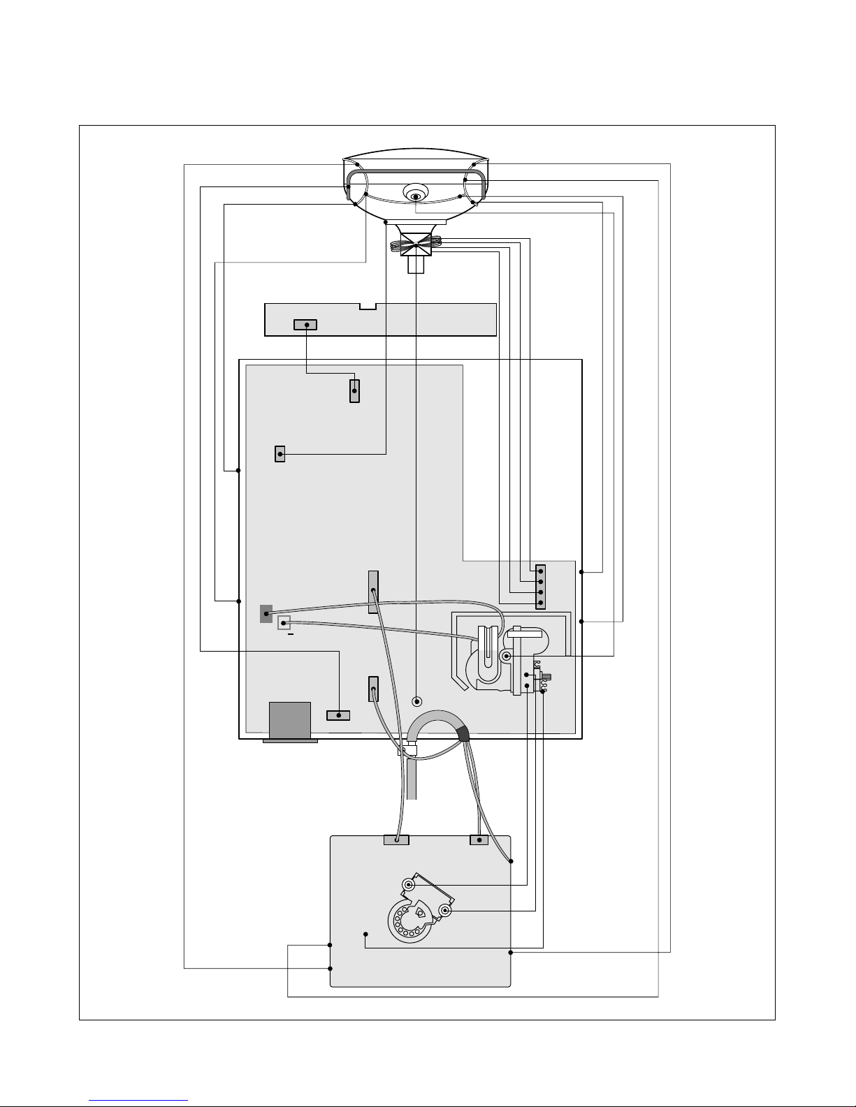
P501
P201
P405
P301
P302
G2
P702
P701
T1
P402
P902
S
+
S
Signal
Cable
AC
Socket
FBT
Page 10
BLOCK DIAGRAM
- 10 -
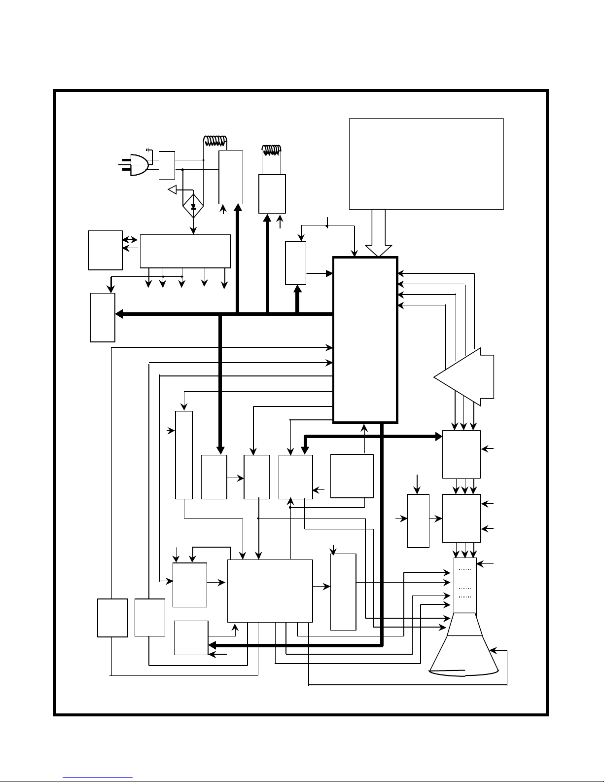
Degaussing
Coil
TILT
100~240V AC
Power Input
(50/60Hz)
Line
Filter
Degaussing
Circuit
Coil
TILT
Control
Circuit
[ OSD Control ]
OSD CONTROL LOCK
TOP/BOTTOM CORNER
VIDEO LEVEL
PAR ALL ELOGR AM
RECALL / RESET
ROTATION (Tilt)
INFORMATION
LANGU AGE
OSD TIME
COLOR
PIN BAL ANC E
H / V POSI TION
DEG AUSSING
TRAPEZOID
H / V SI ZE
SPCC
BRIGHTNESS
CONTRAST
MOIRE
(IC901)
Circuit
E
2
PROM
5V
H-Sync
V-Sync
I
2
C CLOCK(SCL)
(IC302)
(IC303)
I
2
C DATA(SDA)
B
OSD
Main AMP
Signal
Video
R
G
Pre- AMP /
VIDEO
VIDEO
5V
8V 80V
I
2
C
V-Out
13V
MICOM & H/V Sync Processor
SAA4849
( IC 401 )
SCL / SDA
H-Sync/V-Sync
PWM Control Signal
Protection
Circuit
X-R AY
80V
R/G/B
Bias
CUT OFF Circuit
(IC304)
13V
SMPS
Control
Voltage
feedback
5V
DPM
Control
(T901)
SMPS
6.3V
50V
50V
13V
B-Drive
80V
H - Drive
H-Linearity
Correction
( Q706)
H-Out
6.3V
13V
(IC402)
TDA4867J
( IC 601)
5V
Dynamic
FOCUS
Circuit
Regulation
Circuit
Feed Back
D/D
Auto
Beam
LimitDC/DC Converter
B+
( T701 )
FBT
13V
13V
40V
Brightness Control
- 160V
G2
G1
Screen
Static Focus
Dynamic Focus
Heater ( 6.3V )
DY C DT
H.V
Page 11

DESCRIPTION OF BLOCK DIAGRAM
- 11 -
1. SMPS(Switching Mode Power Supply)
When you turn on the power switch, the operating
fprocedure is as follows:
.
6. X-RAY Protection Circuit
When the high Voltage reaches to 29kV in an abnormal case,
the high voltage detector circuit, R818,D721,C739-1 R416,
C409 start operation to shut down high voltage circuit.
7. Horizontal S-correction Circuit.
This circuit corrects the horizontal linearity for each horizontal
sync frequency.
8. Horizontal drive and Output Circuit.
This circuit is a horizontal deflection amplifier for raster scan.
9. ABL Circuit
This circuit limits the beam-current for the reliability of CDT
10. Vertical Output Circuit
This circuit takes the vertical ramp wave from the TDA4867J
(IC601) and perform the vertical deflection by supplying the
saw-tooth wave current to the vertical deflection yoke.
11. Blanking and Brightness Control Circuit.
Blanking circuit eliminates the retrace line by supplying
a negative pulse wave to the G1 of the CDT.
Brightness control circuit is used for control of the screen
brightness by changing the DC level G1.
12. Image Rotation (Tilt) Circuit.
This circuit corrects the tilt of the screen by supplying
the image rotation signal to the tilt coil which is
attached near the deflection yoke of the CDT.
13. OSD (On Screen Display) Circuit.
This circuit displays information of the monitor`s status
on the screen.
14. Video Processor Circuit.
Video processor circuit consists of the video drive output
block. The video drive IC(IC302) receives the video
signal from PC. The gain of each channel is controlled
by MICOM through IIC.
The cut-off circuit compensate different voltage of each
channel between the cathode and the G1 of the CDT.
1) The AC line voltage is rectified by the bridge diode
D900.
2) The control IC(IC901) starts switching and generates
switch pulse in the primary turn of the SMPS
transformer(T901)
3) The switching pulses of the primary turns are induced
to the secondary turns of the transformer by the turn
ratio. This pulses are rectified by each diode(D971,
D961(D962),D951,D942,D941)
4) Each rectified DC voltage(80V, 50V, 13V, 6.3V
and 5V)
2. Over Voltage Protection Circuit
When the input of IC901 Vin (pin 4) is more than 22V, all the
secondary voltages of the SMPS transformer (T901) down
to low value
3. Display Power Management Circuit(DPM)
1) STAND-BY & SUSPEND Mode
When no input of horizontal or vertical sync Q951,
Q941 are turned off and Q952,Q942 are turned off.
Then input power consumption is below 5 watts.
2) OFF Mode
When no input of horizontal and vertical sync Q951,
Q941 are turned off and Q952, Q942 are turned off.
Then input power consumption is below 5 watts.
4. Microprocessor Control & Horizontal and Vertical Sync
Processor Circuit
The operating procedure is as follows ;
1) There is Horizontal & Vertical process function in
Microprocessor.(IC401)
2) Microprocessor (IC401) discriminates the operating mode
from the sync polarity and resolution.
3) After microprocessor reads these adjusted mode data
stored at EEPROM, it controls operating mode data through
IIC
4) Users can control screen condition by the OSD Select,Up,
Down, Left, Right, Exit.
5. D/D Converter Circuit.
To obtain constant high voltage, this circuit supplies
controlled DC voltage for FBT and horizontal deflection
circuit according to the horizontal sync frequency.
Page 12

- 12 -
15. Video Pre-Amp Circuit.
This circuit amplifies the analog video signal from 0~0.7 V
to 0~4 V. It is operated by taking the clamp, R,G,B drive
and contrast signal from the MICOM (IC401)
16. Video Output Amp Circuit.
This circuit amplifies the video signal which comes from the
video pre-amp circuit and amplified it to applied the CDT
cathode
Page 13

1. Preparation for Service Adjustment
GENERAL INFORMATION
All adjustment are thoroughly checked and corrected
when the monitor leaves the factory, but sometimes
several adjustments may be required.
Adjustment should be following procedure and after
warming up for a minimum of 30 minutes.
• Alignment appliances and tools.
- IBM compatible PC.
- Programmable Signal Generator.
(eg. VG-819 made by Astrodesign Co.)
- EPROM or EEPROM with saved each mode data.
- Alignment Adaptor and Software.
- Digital Voltmeter.
- White Balance Meter.
- Luminance Meter.
- High-voltage Meter.
AUTOMATIC AND MANUAL DEGAUSSING
The degaussing coil is mounted around the CDT so that
automatic degaussing when turn on the monitor. But a
monitor is moved or faced in a different direction, become
poor color purity cause of CDT magnetized, then press
DEGAUSSING on the OSD menu.
ADJUSTMENT PROCEDURE & METHOD
- Install the cable for adjustment such as Figure 1and run
the alignment program on the DOS for IBM
compatible PC.
- Set external Brightness and Contrast volume to max
position.
1. Adjustment for B+ Voltage.
1) Display cross hatch pattern at Mode 4.
2) Check D961 cathode voltage within 50V ± 1V .
2. Adjustment for High-Voltage.
1) Display cross hatch pattern at Mode 4.
2) Enter the SVC SUB menu as the following instruction.
3) Adjust H/Voltage to 25.8kV±0.1 kV by adjust 1-P value.
2. Adjustment by Service Hot key
How to enter SVC HOT KEY
1. Press Menu and OSD window will appear.
2. While OSD window is displayed,
is seen on the
left bottom of OSD window.
3. Press + power switch simultaneously and the
screen will immediately refresh.
4. Press Menu and make sure that is changed to
1 2.
5. Follow the menu on the left of OSD window to find 12
and OSD will change as shown in the figure.
6. Select Degauss in the above figure and then press
Select and
to enter the screen of the SUB menu.
(Back Raster for Pattern)
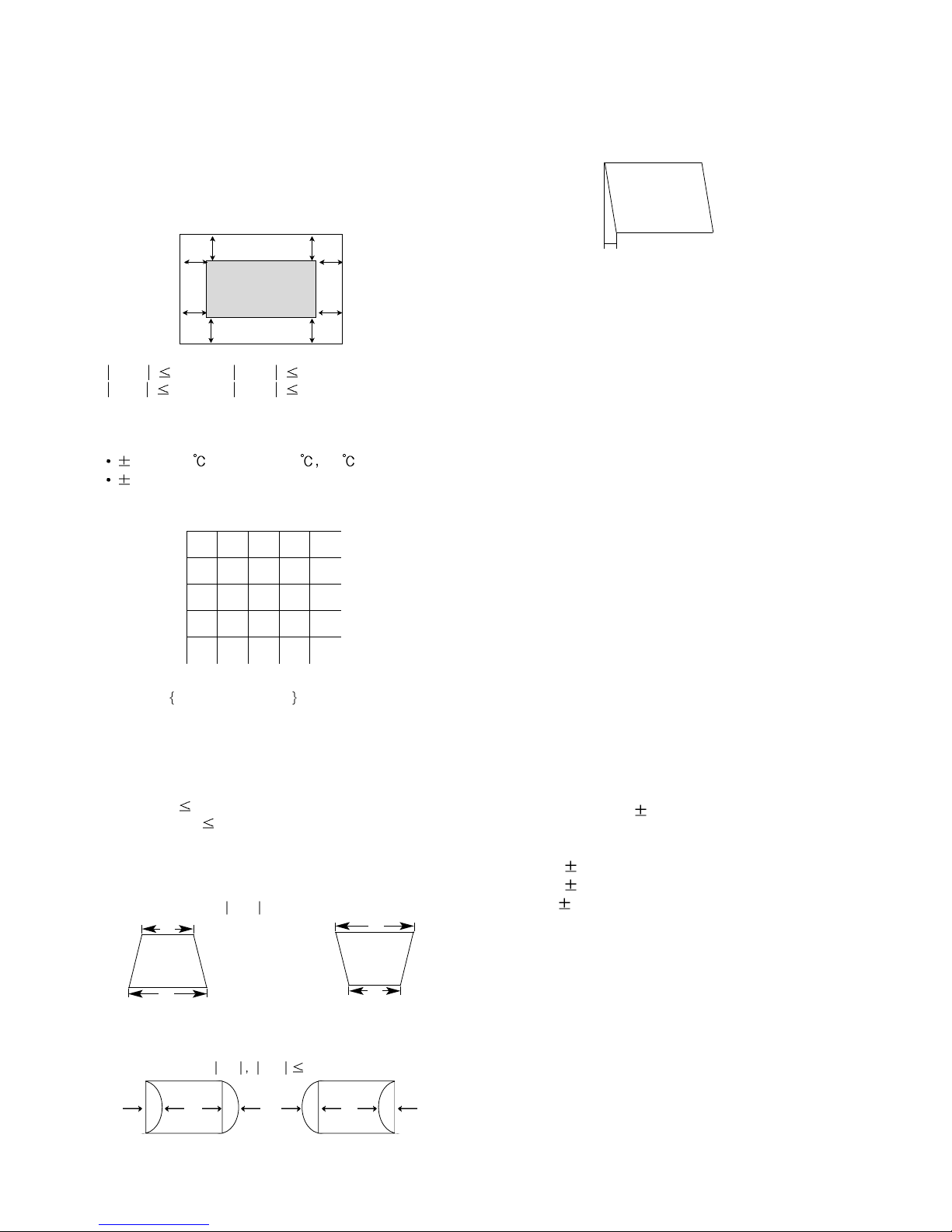
FOS SPEC
1. Size
H : 310
4mm
V : 230
4mm
Scanning frequency : All Mode (Mode 1~4)
Display image : Cross hatch pattern
2. Centering
Scanning frequency : All Mode (Mode 1~4)
Display image : Crosshatch pattern
Horizontal : 10 Row
Vertical : 8 Row
H :
L-R 4mm, V : U-D 4mm
3. Tilt
Scanning frequency : All Mode (Mode 1~4)
Display image : Crosshatch pattern
Horizontal : 10 Row
Vertical : 8 Row
Tilt :
E-F 2.0mm
- 13 -
ADJUSTMENT
U
D
L
R
EF
Page 14
- 14 -
4. Distortion
Scanning frequency : All Mode (Mode 1~4)
Display image : Crosshatch pattern
Horizontal : 10 Row
Vertical : 8 Row
A-B 2.0mm, C-D 2.0mm
E-F 2.0mm, G-H
2.0mm
5. Displa Size drift
4mm : 25 Standard, 10 35
0.5mm : 180V ~ 264V
6. Linearity
Formula :
(Max - Min) / Max
x 100(%)
Criteria : H - 10% Max. (Upper 40kHz)
14% Max. (Less 40kHz)
V - 8% Max.
7. Regulation
Luminance
2mm
Dynamic(lode) 2mm
Scanning frequency : All Mode (Mode 1~4)
8. Trapezoid
9. Pin Balance
10.Parallelogram
11. Adjustment of white balance (Adjustment of
chromaticity diagram)
*(Adjustment of white balance must be made after
entering Hot Key Mode and DEGAUSS.)
CONDITIONS
Signal: 69 kHz / 85 Hz
Display image: Back raster (Color 0,0)
Contrast: Maximum
Brightness: Maximum
Color temperature: 9300K
11-1. Adjustment of cut off (Adjustment of back raster)
11-1(a). Before adjustment, press Menu and Degauss
to remove.
=> Enter hot key mode.
Adjust Brightness and Contrast to Max in OSD
window.
(1)Adjust cut off (back raster) first. Enter DEGAUSS in
the Menu and modify the following data.
Modify RCUT to Min ,
Modify GCUT To Min ,
Adjust to BCUT Data = 127 (7F (h)) ,
Adjust to SBRT Data = 205 ( CD (h)).
(2)Turn FBT screen volume on "CRT COLOR
ANALYZER CA-100" equipment to adjust
Brightness to 0.4
0.05FL.
(3)Adjust RCUT, GCUT, and SBRT to set chromaticity
diagram at :
x: 0.283
0.005
y: 0.298 0.005
Y: 0.40
0.05FL
* If color values would not be matched desirable values,
repeat sequence 1 and 2 after readjusting “GREEN
CUTOFF” control a little different.
U
D
D
U
U-D
< 4mm
L1 R1
2.0mm
L1
R1 L1
R1
Y1
Y2
Y3
Y4
X1 X2 X3 X4
4mm
A B
DC
EG
FH
Page 15
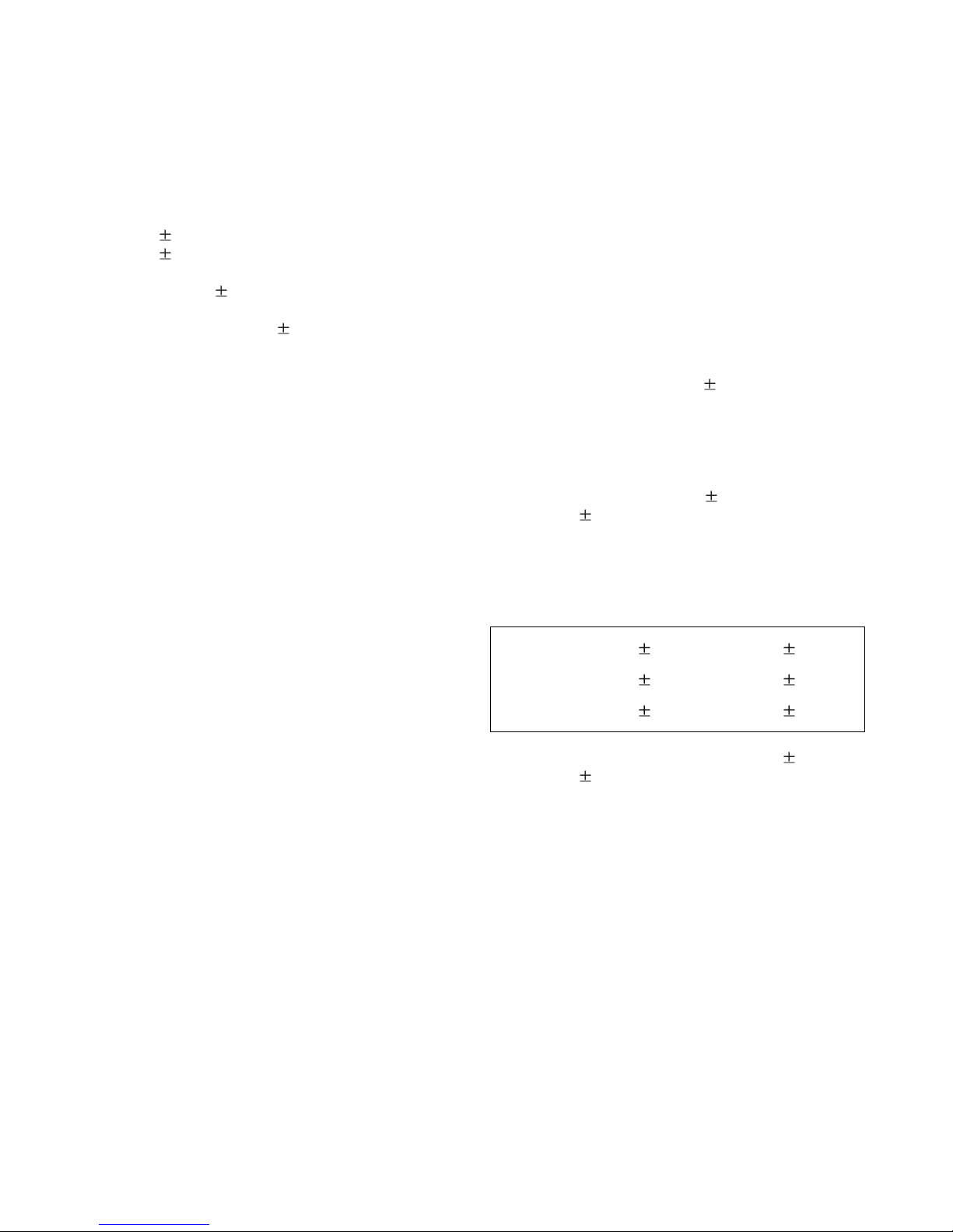
11-2. Adjustment of White Balance
After finishing adjustment of cut off (back raster),
approve "Color(15.0) Full white pattern".
Adjust BDRV Data = 90, SCON=127.
Adjust RDRV and GDRV to set chromaticity diagram at :
x: 0.283 0.005
y: 0.298 0.005
Approve "Window pattern (70x70mm)" to adjust
S-CON to Y : 50 1FL.
Approve "Color (15.0) Full white pattern" again and
adjust ABL Data to Y : 32 1FL
PROCEDURE
For trained and experienced service technicians only.
Use the following procedure to correct minor color
purity problems:
1. Make sure the display is not affected by external
magnetic fields.
2. Very carefully break the glue seal between the 2-pole
purity convergence magnets (PCM), the band and
the spacer.
12. Focus Adjustment
CONDITIONS
Scanning frequency : All Mode (Mode 1~4)
Display image: ÒHÓ character pattern
Brightness: Cut off point
Contrast: Maximum
PROCEDURE
1. Adjust the Focus VR on the FBT to display the
sharpest image possible.
2. Use Locktite to seal the Focus VR in position.
13. Color Purity Adjustment
Color purity is the absence of undesired color.
Conspicuous mislanding (unexpected color in a uniform
field) within the display area shall not be visible at a
distance of 50 cm from the CRT surface.
CONDITIONS
Orientation: Monitor facing east
Scanning Frequency: 1024 x 768@85Hz(69kHz/85Hz)
Display image: White flat field
Luminance: Cut off point at the center of the
display area
Note: Color purity adjustments should only be
attempted by qualified personnel.
3. Make sure the spacing between the PCM assembly
and the CRT stem is 29 mm
1 mm.
4. Display a green pattern over the entire display area.
5. Adjust the purity magnet rings on the PCM assembly
to display a pure green pattern.
(Optimum setting: x = 0.295
0.015,
y = 0.594 0.015)
6. Repeat steps 4 and 5 using a red pattern and then
again, using a blue pattern.
Table 4-6. Color Purity Tolerances
Red: x=0.620 0.015 y=0.334 0.015
Green: x=0.620 0.015 y=0.334 0.015
Blue: x=0.620 0.015 y=0.334 0.015
(For 9300K color adjustment: x = 0.283 0.02,
y = 0.298 0.02)
7. When you have the PCMs properly adjusted,
carefully glue them together to prevent their
movement during shipping.
- 15 -
Page 16

- 16 -
3. Adjustment Using Service software Program
(Adjustment Program)
1. Adjustment for Factory Mode (Preset Mode).
1) Display cross hatch pattern at Mode All.
2) Run alignment program for T710BHL on the IBM
compatible PC.
3) EEPROM → ALL CLEAR → Y(Yes) command.
<Caution> Do not run this procedure unless the
EEPROM is changed. All data in EEPROM (mode
data and color data) will be erased.
4) COMMAND → PRESET START → Y(Yes)
command.
5) DIST. ADJ. → FOS. ADJ command.
6) Adjust H-POSITION as arrow keys to center of the
screen.
7) Adjust H-SIZE as arrow keys to 310 ± 2mm.
8) Adjust V-POSITION as arrow keys to center of the
screen.
9) Adjust V-SIZE as arrow keys to 230 ± 2mm.
10) Adjust TRAPEZOID as arrow keys to be the best
condition.
11) Adjust SIDE PINCUSHON as arrow keys to be the
best condition.
12) Adjust TILT as arrow keys to be the best condition.
13) Display cross hatch pattern at Mode 4.
14) DIST. ADJ. → BALANCE DATA command.
15) Adjust balance of Pin-Balance as arrow keys to be
the best condition.
16) Adjust parallelogram as arrow keys to be the best
condition.
17) Save of the Mode.
18) Save of the System.
19) Display from Mode 4 and repeat above from number
6) to 16).
20) COMMAND → PRESET EXIT → Y (Yes) command.
2. Adjustment for White Balance and Luminance.
1) Set the White Balance Meter.
2) Press the DEGAUSSING on the OSD menu for
demagnetization of the CDT.
3) Display color 0,0 pattern at Mode 4.
4) COMMAND → PRESET START → Y(Yes)
command.
5) Set Bightness and Contrast to max position.
6) COLOR ADJ. → LUMINANCE command of the
alignment program.
7) COLOR ADJ. → BIAS ADJ. command of the
alignment program.
8) Check whether blue color or not at R-BIAS and GBIAS to min position, Sub-Brightness to 205
(CD(h))position, B-Bias to 127(7F(h))position. If it's not
blue color, the monitor must repair.
9) Adjust Screen control on the FBT to 0.4 ± 0.05FL
of the raster luminance.
10) Adjust R-BIAS and G-BIAS command to x=0.283 ±
0.006 and y=0.298 ± 0.006 on the White Balance
Meter with PC arrow keys.
11) Display color 15,0 Full White(70x70mm) at mode 4.
12) DRIVE ADJ command.
13) Set B-DRIVE to 90(5A(h)) at DRIVE of the alignment
program.
14) Adjust R-DRIVE and G-DRIVE command to white
balance x=0.283 ± 0.003 and y=0.298 ± 0.003 on
the White Balance Meter with PC arrow keys.
15) Adjust SUB-CONTRAST command to 50±1FL of the
raster luminance.
15)Display color 15,0 full white patten at Mode 4.
16) COLOR ADJ. → LUMINANCE → ABL command.
17) Adjust ABL to 32 ± 1FL of the luminance.
18) Exit from the program.
Page 17
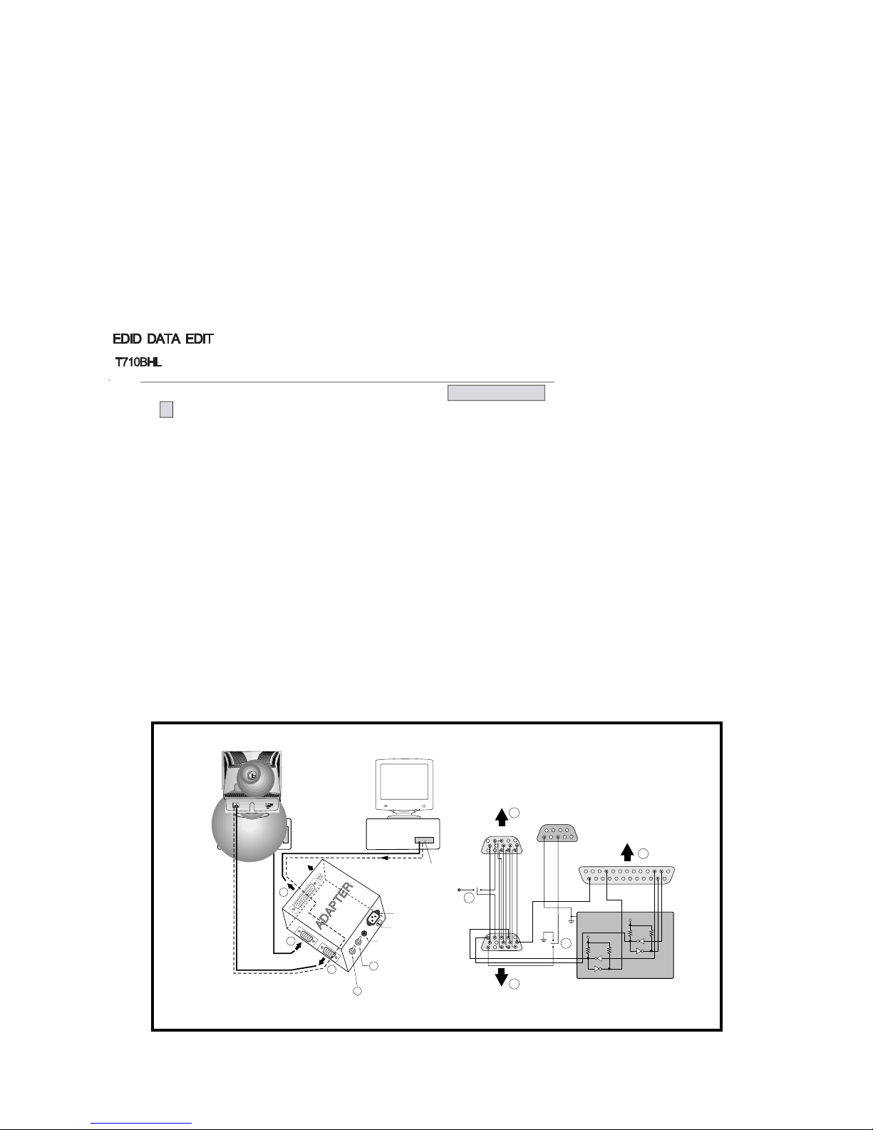
4. EDID Data Edit Using Service software Program
4.1 Read and Modify EDID Data
1) Connector the monitor and adjust device as Figure1
2) Display color 15,0 cross hatch pattern at Mode 4.
3) Use EDIT – MODEL SEL. command to select the right model info file.
4) Use EDIT – EDID INFO command and return to read the EDID Data.
5) Modify the EDID Data if needed and using F10 to save the change and exit.
4.2 Write EDID Data.
1) Display color 15,0 cross hatch pattern at Mode 4.
2) Use EEPROM -- Write EDID command and confirm
“EDID Write OK!!” message of monitor.
3) Exit from the alignment program.
4) Power switch OFF/ON for EDID data save.
- 18 -
000102030405060708090A0B0C0D0E0F
00|00FFFFFFFFFFFF001E6D6643*01000000
10|**010E0103182118B5EAF629A253479925
20|10484CFFFE803159714F455961598180
30|814A01010101EA240060410028303060
40|130036E61000001E000000FD0032A01E
50|470B000A202020202020000000FC0054
60|37313042480A202020202020000000FC
70|000A20202020202020202020202000***
- 18 -
220
IB M
Co mpatible P C
PA R ALL EL P OR T
Powe r inlet (re quired)
Powe r LE D
S T S witch
Powe r S elec t Switch
(110 V/220V )
Co ntrol Line
No
t u
s
e
d
RS 2
3
2
C
PA
RAL
L
EL
V
-
SY N
C
P
O
WE
R
S
T
V
GS
M
ONIT
OR
E
V-S ync On/Off Switch
(S witch mus t be O N.)
F
A
B
C
E
F
A
B
C
15
10
5
5
69
1
1
1
14
13
25
6
5V
5V
5V
4.7K
4.7K
4.7K
74LS 06
74LS 06
OF F O N
OF F
ON
11
VI DE O
S IGN AL
GE N ER A TOR
Figure 1. Cable Connection Figure 1. Cable Connection
T710BL
0 1 2 3 4 5 6 7 8 9 A B C D E F
00 FF FF FF FF FF FF 00 1E 6D #65 #43 *01 *01 *01 *01
**01 ***DE 01 03 18 21 18 B5 EA F6 29 A2 53 47 99 25
10 48 4C FF FE 80 31 59 71 4F 45 59 61 59 81 80
81 4A 01 01 01 01 EA 24 00 60 41 00 28 30 30 60
13 00 36 E6 10 00 00 1E 00 00 00 FD 00 32 A0 1E
47 0B 00 0A 20 20 20 20 20 20 00 00 00 FC 00 54
37 31 30 42 0A 20 20 20 20 20 20 20 00 00 00 FC
00 0A 20 20 20 20 20 20 20 20 20 20 20 20 00 **
Page 18
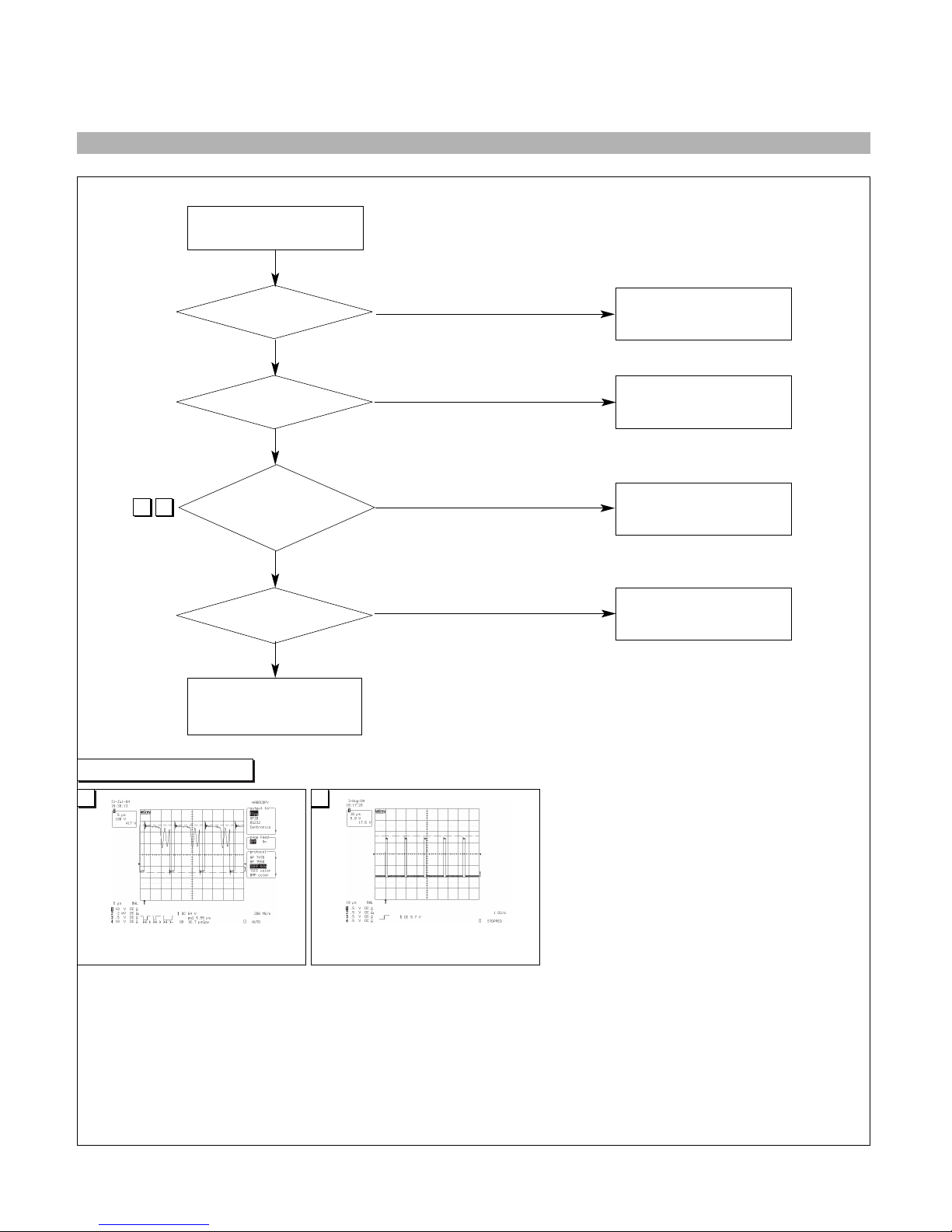
1 2
CHECK
D900 BRIDGE DIODE?
CHECK
C908(+) VOLTAGE
145VDC at 110V input
310VDC at 220V input
IC901, Q901
CHECK
D971, D961, D951, D904
D941, D942, D906 ?
CHECK
FUSE OK?(F901)
- 18 -
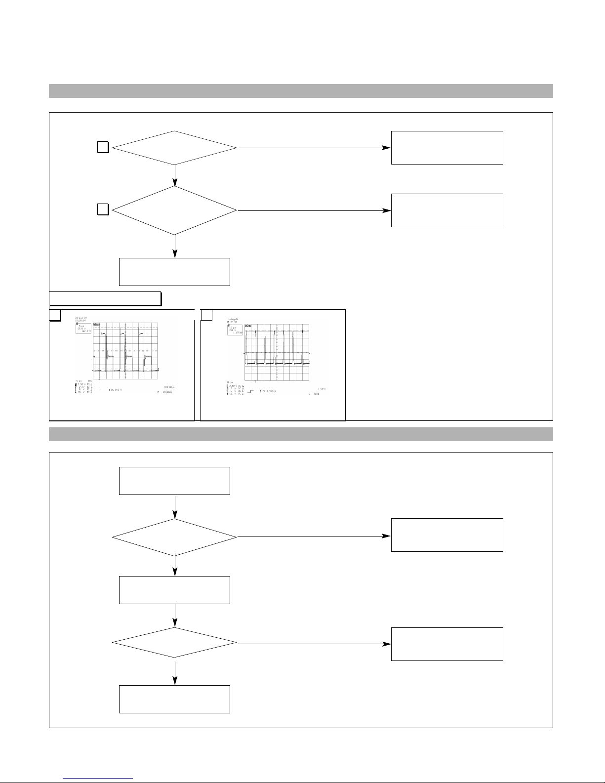
TROUBLESHOOTING GUIDE
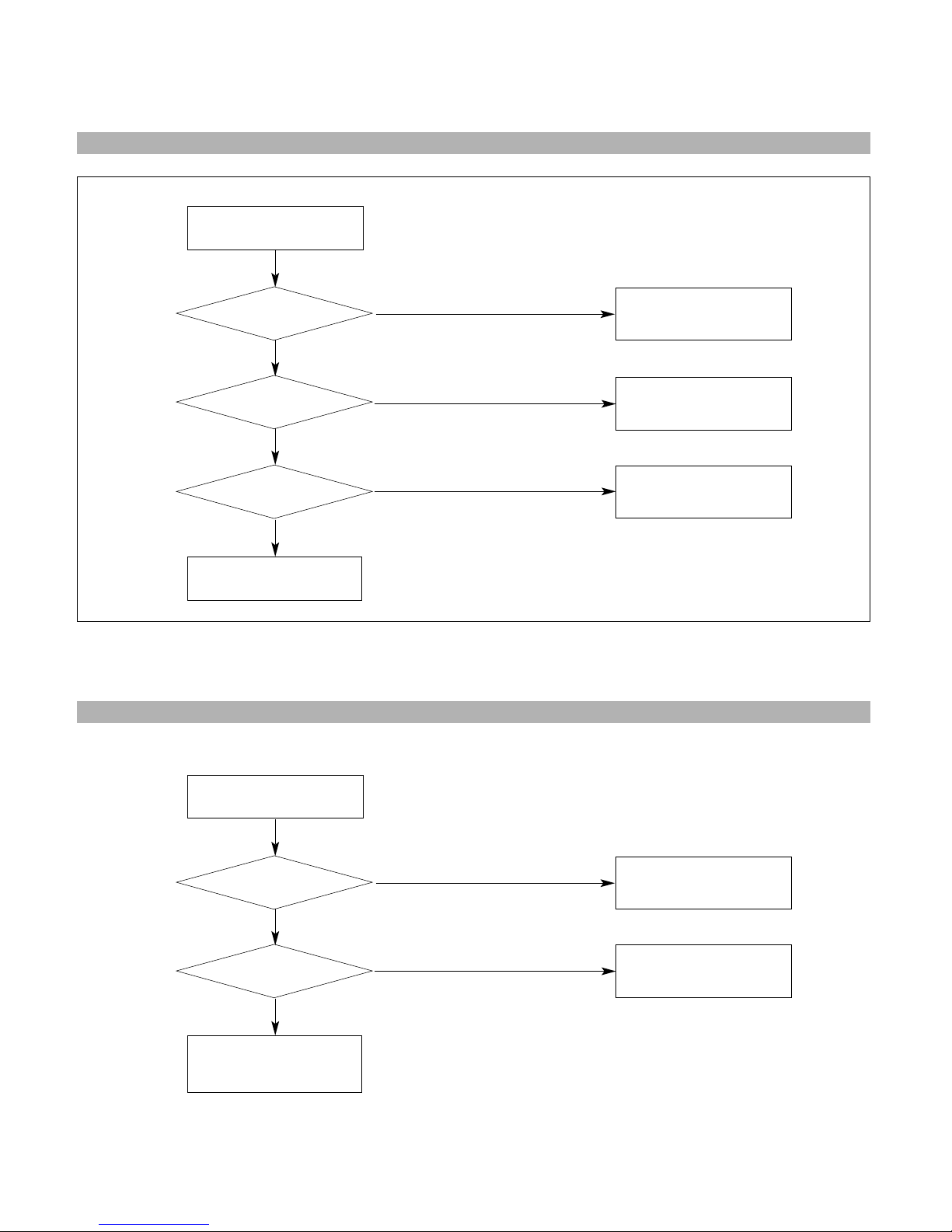
1. NO POWER
NO POWER
(POWER INDICATOR OFF)
NO
NO
NO
NO
TROUBLE IN
Q951, Q952, Q941, Q942,
TROUBLE
IN FUSE (F901)
SMPS Switch (ON, OFF)
Waveforms
TROUBLE IN
BRIDGE DIODE (D900)
TROUBLE IN
IC901, Q901
TROUBLE IN
D971, D961, D951, D904
D941, D942, D906
YES
YES
YES
YES
Q901, Drain IC901, #6
21
Page 19
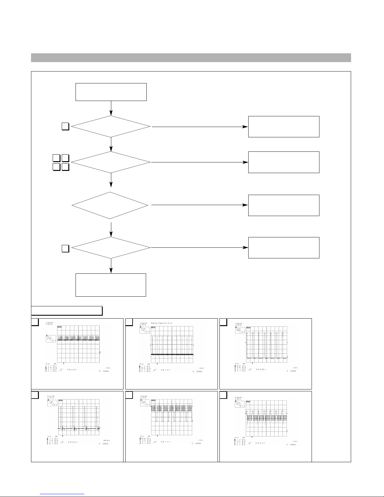
26
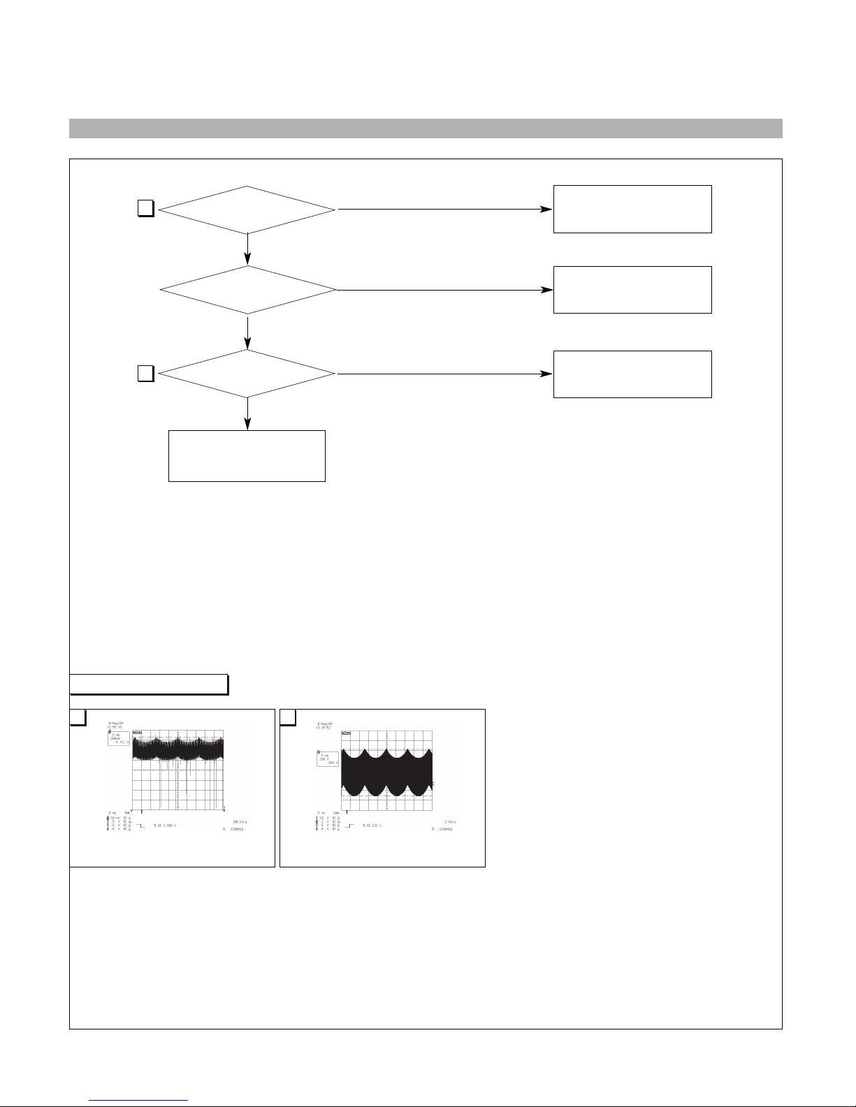
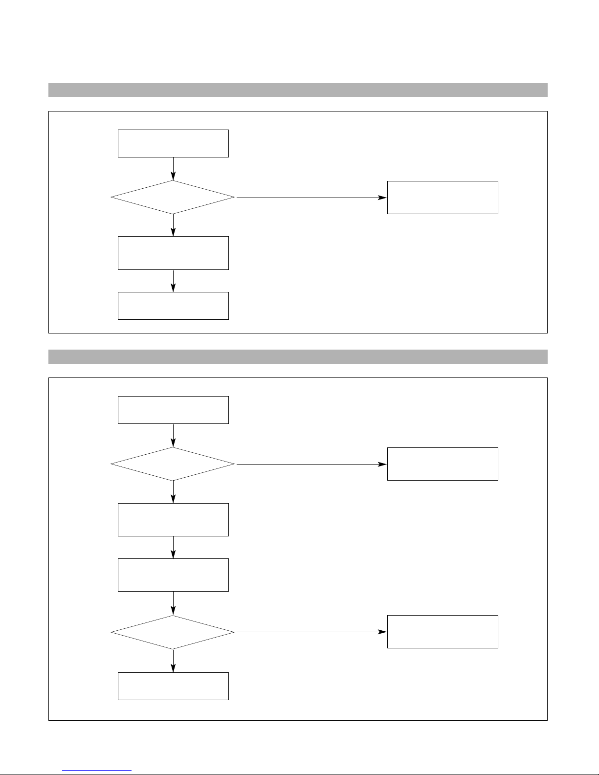
2. NO CHARACTER
NO CHARACTER
NO
NO
NO
NO
TROUBLE IN
CDT SOCKET
TROUBLE IN
P301, SIGNAL CABLE,
PC SIGNAL
TROUBLE IN
IC302, P301
TROUBLE IN
IC303
TROUBLE IN
IC304
YES
YES
YES
YES
- 19 -
CHECK
IC302 PIN 5,6,7
CHECK
IC302 PIN 1, 24, 23, 19, 20, 21
PIN 18 (5V) ?
CHECK
IC303 PIN 1, 2, 3
PIN8 (8V),
PIN 4 (80V) ?
CHECK
R, G, B CATHODE
VOLTAGE?
IC302, #5, 6, 7
IC302, #23 IC302, #19, 20, 21
IC302, #1 IC302, #24
CDT, RK, GK, BK
Waveforms
2827
30
31
26 27 28
29 30 31
29
Page 20
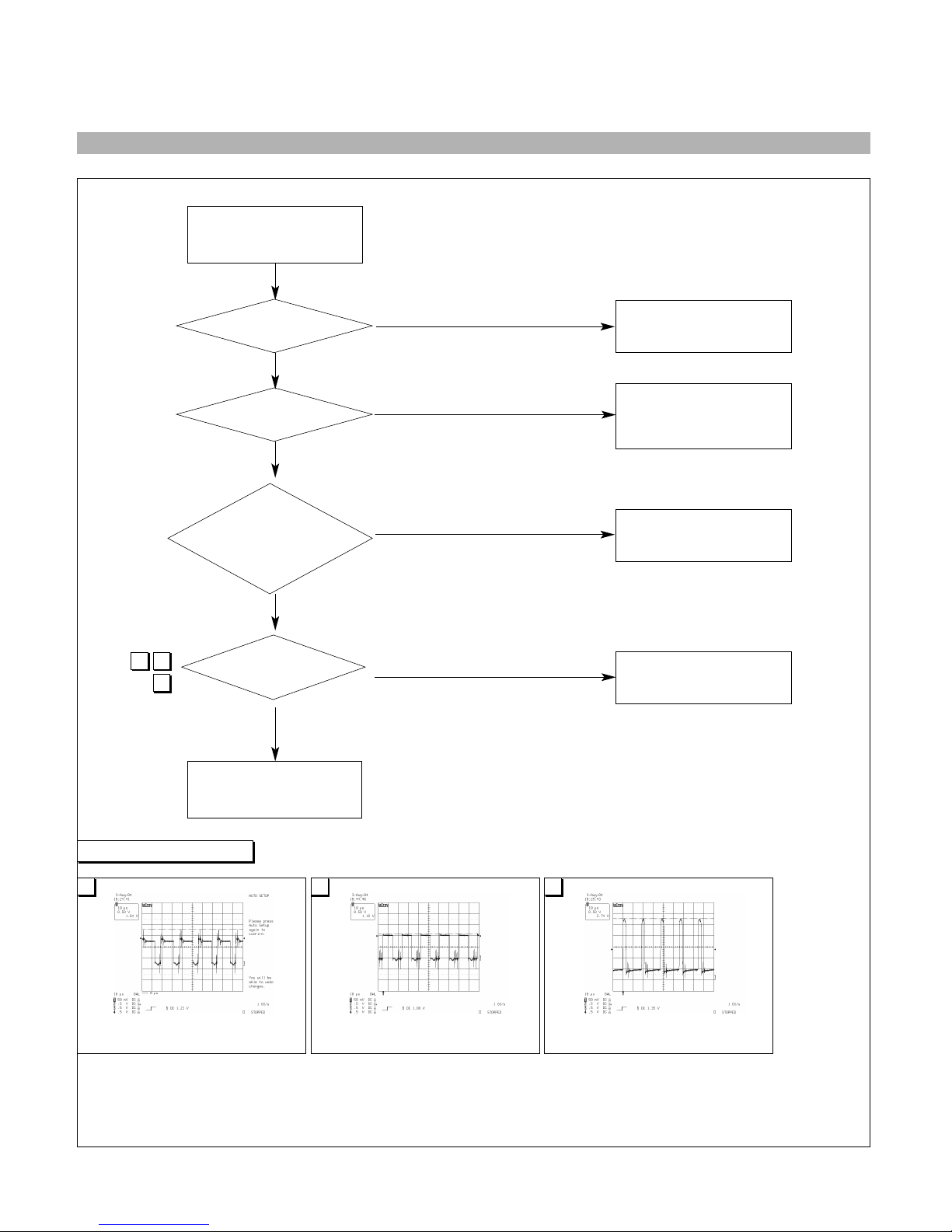
CHECK
SCREEN CONTROL
KNOB OF FBT
CHECK
VOLTAGE AT
D961 CATHODE (50V)
D971 CATHODE (80V)
D951 CATHODE (13V)
D941 CATHODE
(6.3V)?
CHECK
IC401 (MICOM) PIN 16
5V (HIGH), IC401 PIN 18
PIN20, PIN21
CHECK
POWER INDICATOR
GREEN or FLASH ?
- 20 -
3. NO RASTER
FLASH
NO
NO
NO
TROUBLE IN
IC401 (MICOM),
TROUBLE IN
P302 SIGNAL CABLE
ROTATE SCREEN CONTROL
KNOB TO CLOCKWISE
or COUNTER CLOCKWIES
TROUBLE IN PRIMARY
CIRCUIT OF T901
TROUBLE IN
CDT SOCKET, BOARD
GREEN
YES
YES
YES
NO VIDEO
(POWER INDICATOR
GREEN or FLASH)
IC401, #18 IC401, #20 IC401, #21
1475
5 14 7
Waveforms
Page 21
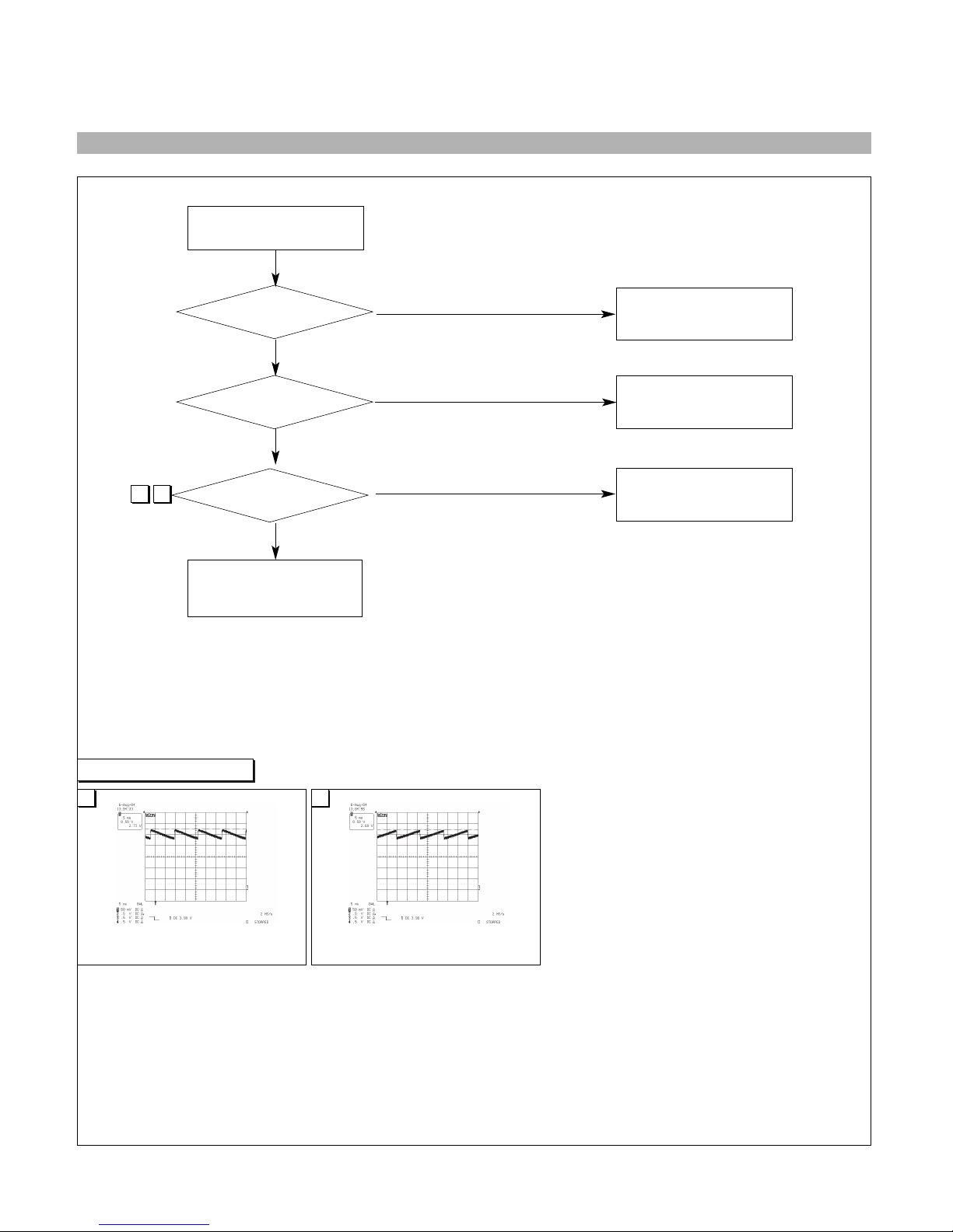
CHECK
IC601 PIN 7 (45V)?
CHECK
IC401 PIN 33, 34
(SAWTOOTH WAVE)?
CHECK
IC601 Pin 3 (13V) ?
- 21 -
4. NO VERTICAL DEFLECTION
NO V-DEFLECTION
(ONE HORIZONTAL LINE)
NO
NO
NO
TROUBLE IN
IC601, V-CIRCUIT
TROUBLE IN
T901 13V Line
Waveforms
TROUBLE IN
T701 40V line
TROUBLE IN
IC401
YES
YES
YES
IC401, #33 IC401, #34
98
8 9
Page 22
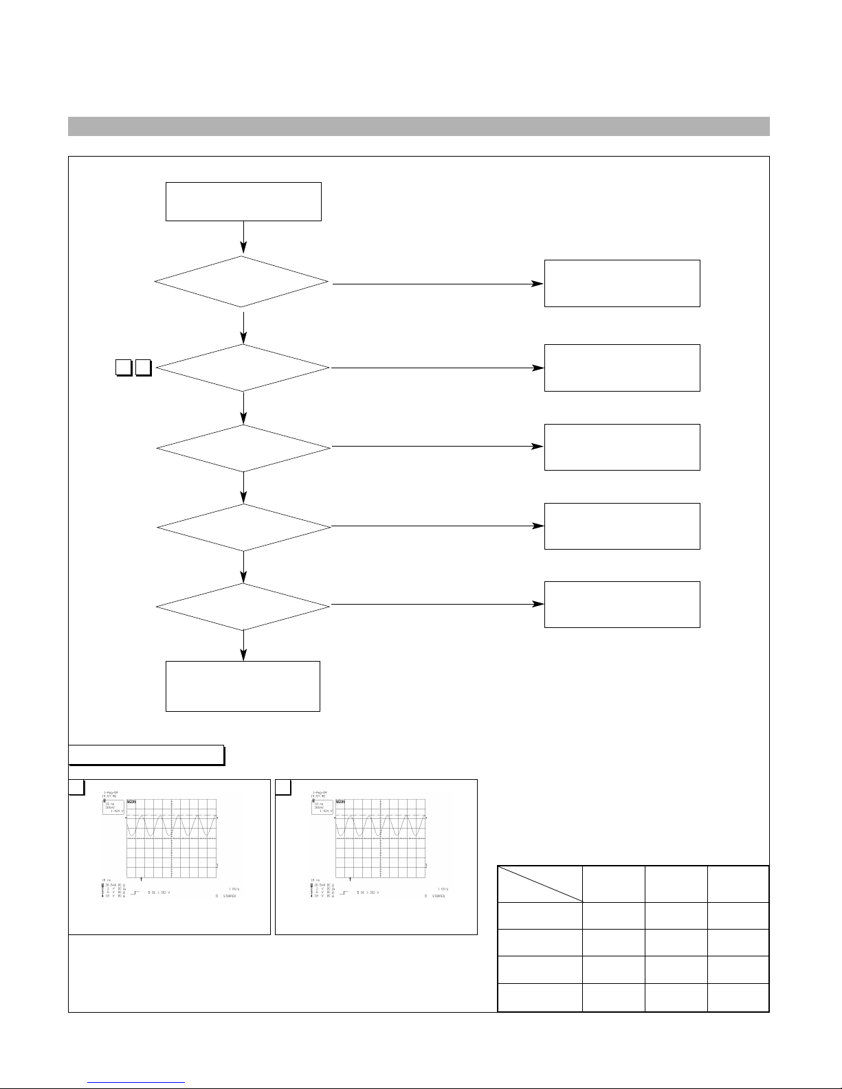
3
CHECK
IC401 PIN 45, 46
WAVEFORM?
CHECK
IC401 PIN 10, 50 ?
CHECK B+ LINE
(50V, 13V, 80V, 5V) ?
CHECK
IC401 (MICOM)
PIN 52, 53 (H/V INPUT)
SIGNAL?
- 22 -
5. TROUBLE IN DPM
4
Stand-by/SUSPEND/
DPMS OFF MODE FAILURE
INPUT H/V SYNC SIGNAL
NO
NO
NO
TROUBLE IN
T901 or PC
CHECK PC,
(PC IS NOT GOING INTO DPM
MODE)
TROUBLE IN
X401, IC401
TROUBLE IN
IC401
TROUBLE IN
IC401
NO
TROUBLE IN
Q941, Q951
NO H/V SYNC SIGNAL
YES
YES
YES
YES
DPMS TABLE
NORMAR ON/ON NORMAL GREEN
STAND-BY OFF/ON OFF(0V) FLASH
SUSPEND ON/OFF OFF(0V) FLASH
OFF OFF/OFF OFF(0V) FLASH
H/V SYNC VIDEO LED
MODE
ITEM
C401, #45 IC401, #46
CHECK
IC401 PIN 16 (5V, HIGH)?
43
Waveforms
Page 23
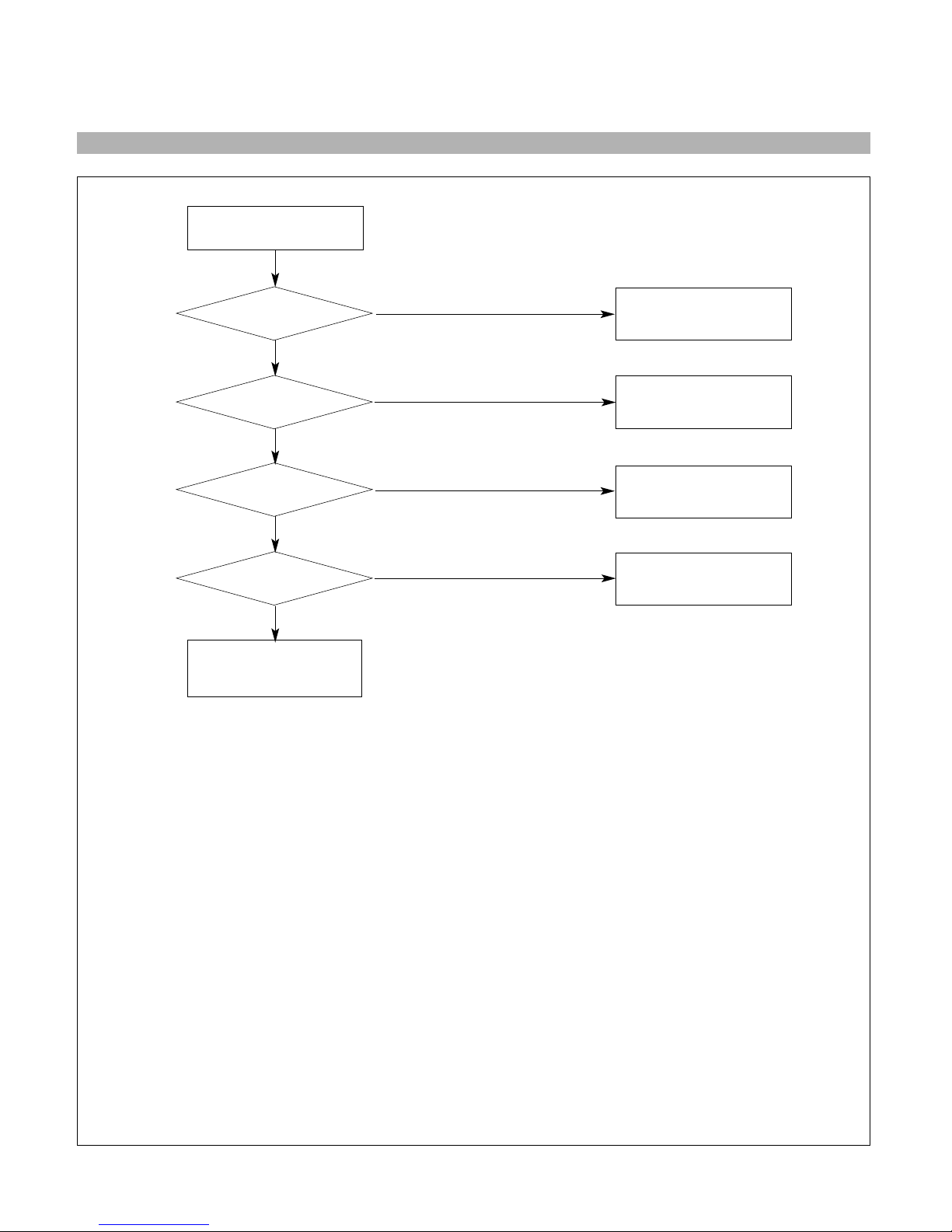
CHECK
Q953 COLLECTOR
VOLTAGE (0.5V)?
CHECK
P902?
CHECK
RL901?
CHECK
IC401 PIN 4 (5V)?
6. NO DEGAUSSING
NO DEGAUSSING
NO
NO
NO
NO
TROUBLE IN
TH901,
DEGAUSSING COIL
TROUBLE IN
IC401 (MICOM)
TROUBLE IN
D953
TROUBLE IN
P902
TROUBLE IN
RL901
YES
YES
YES
YES
- 23 -
Page 24
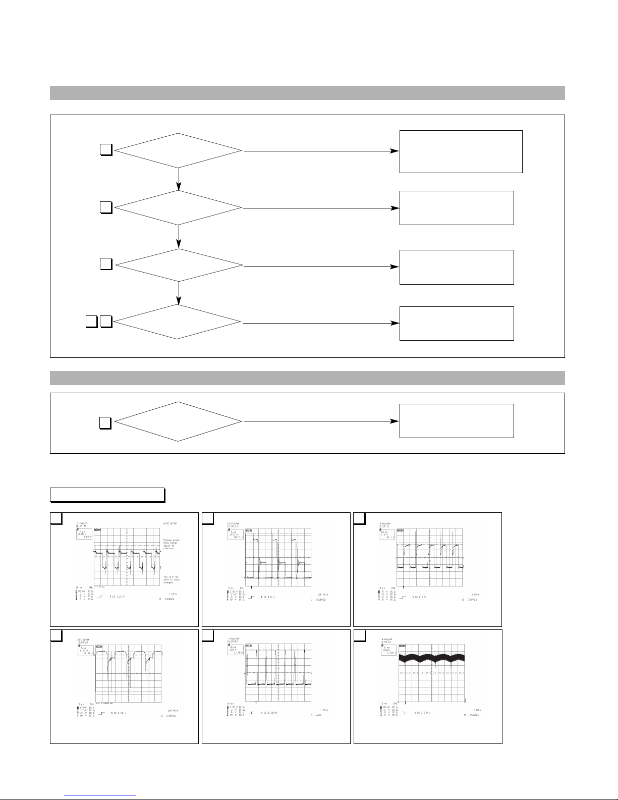
5 18
20 21
19
Q705 drain
waveform is right?
Q706 base, collector
waveforms are right?
Q719 drain
waveform is right?
IC401 Pin 18 waveform is
right?
- 24 -
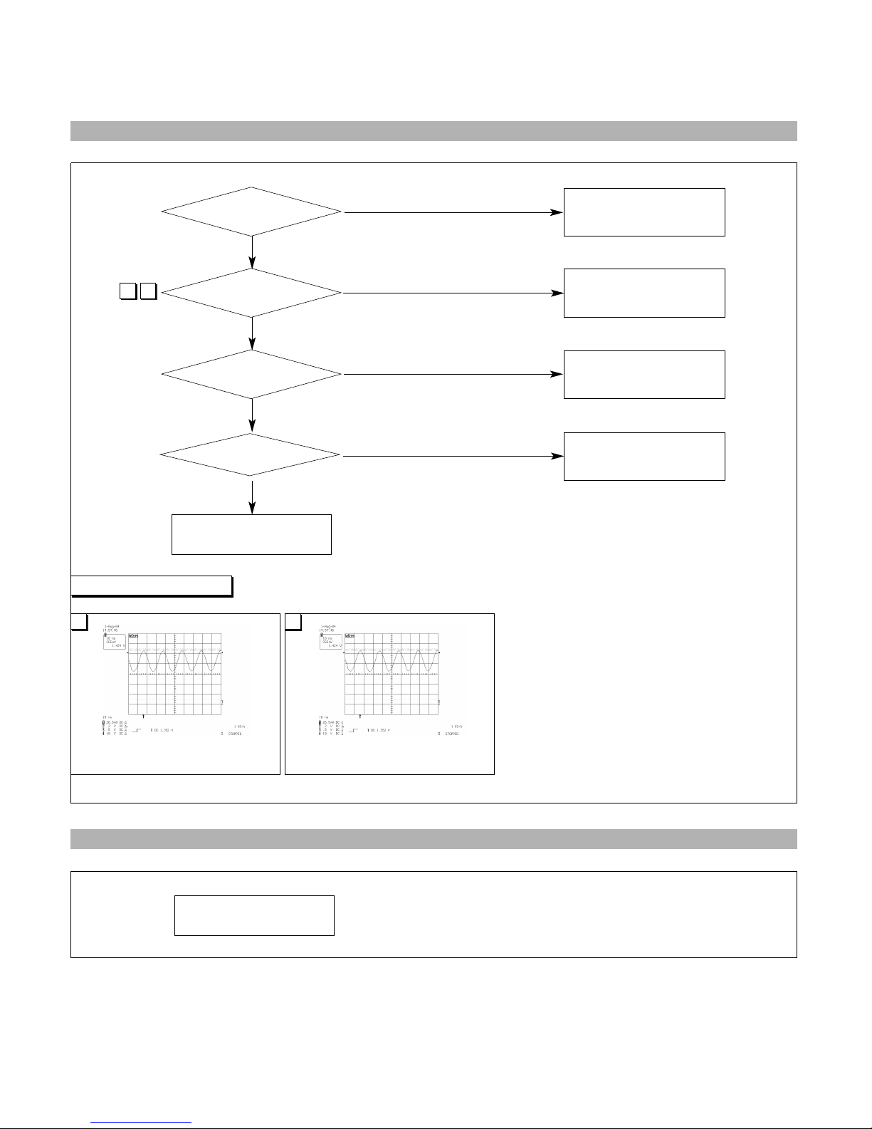
7. H_Deflection Failure
NO
NO
NO
NO
1. Check IC401 Pins 39,40,41
2. Replace IC401.
Check Q720,50V LINE
D710
Check Q704
Check 13V line.
Check and replace T703
and Q706.Check DY connector
connection.
YES
YES
YES
IC401, #18
Q706, Base Q706, Collector
Q719, Drain Q705, Drain
5
18
19
2120
Waveforms
8. Invariable H_Size
NO
Check and replace IC401.
Check if DC voltage of
IC401 PIN 35
wave is Variable.
6
IC401, #35
6
Page 25
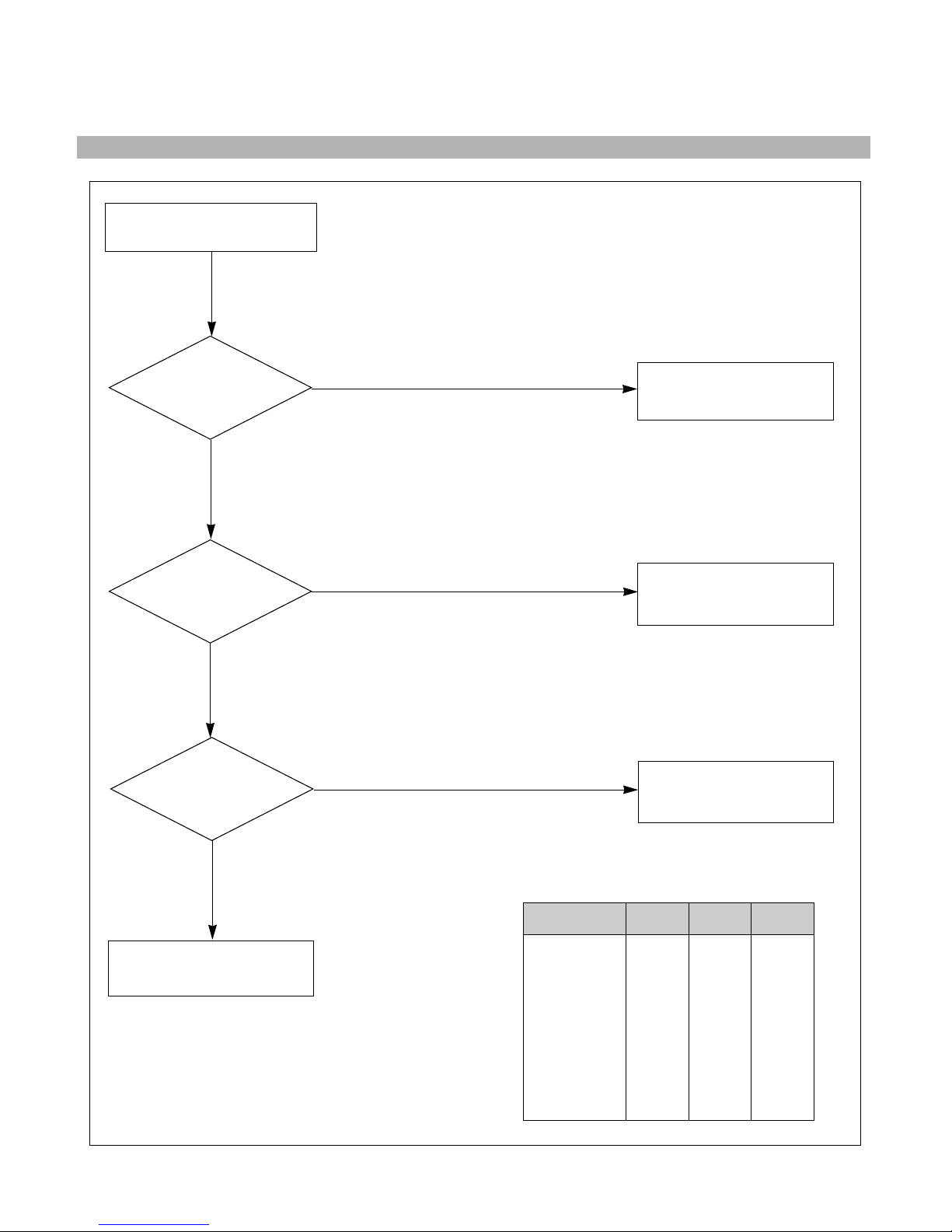
- 25 -
9. TROUBLE IN H-LINEARITY
UNBALANCED OF H-LIN.
CHECK
IC401
PIN 11, 12,13
CHECK
Q711~Q716?
CHECK
L703?
TROUBLE IN
IC401 (MICOM)
TROUBLE IN
Q711 ~ Q716
TROUBLE IN
L703
TROUBLE IN
C722, C723, C726, C729
NO
NO
NO
YES
YES
YES
Cs SIGNAL TABLE
HORIZONTAL
FREQUENCY(fH)
30K ~ 33.9K
34K ~ 38.9K
39K ~ 43.9K
44K ~ 48.9K
49K ~ 51.9K
52K ~ 57.9K
58K ~ 61.9K
62K ~ 65.9K
66K ~ 71K
Cs1
L
L
H
H
H
H
H
H
H
Cs3
L
L
L
L
L
L
L
H
H
Cs2
L
H
L
L
H
H
H
H
H
Page 26
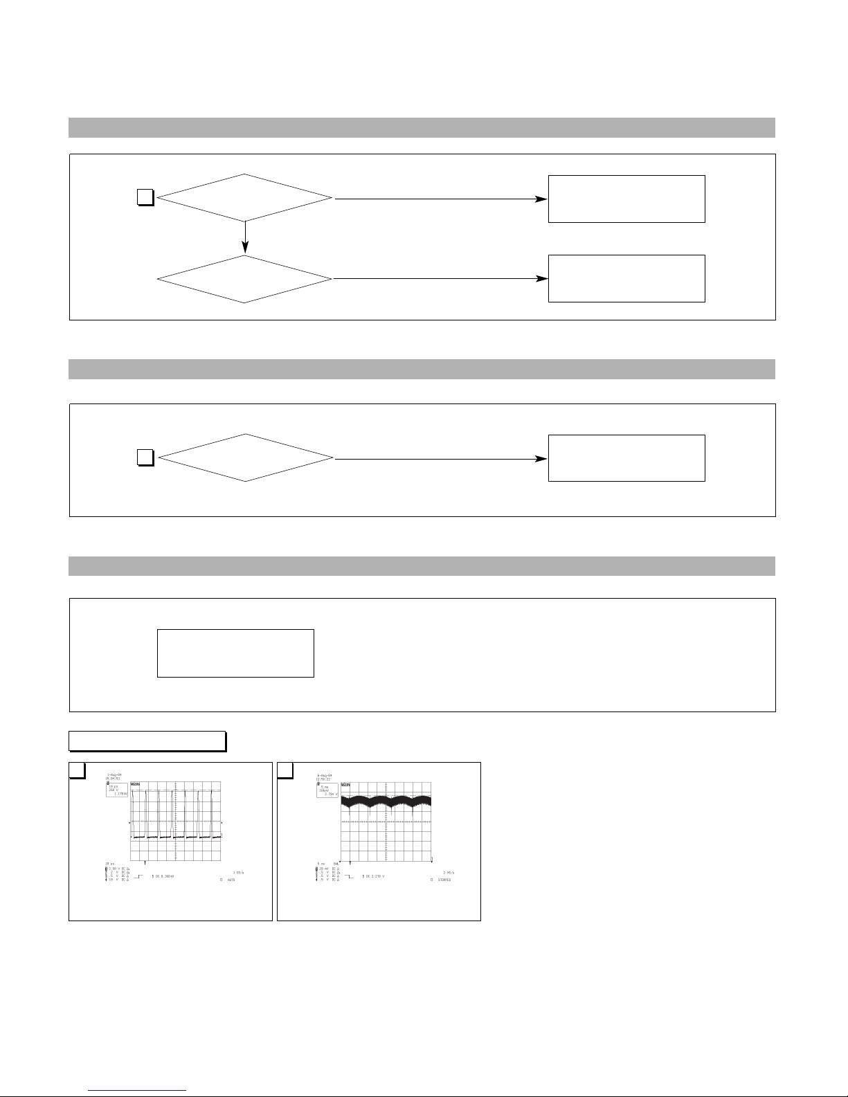
Check if AC
Voltage of IC401 Pin 35
waveform is Variable
T701 pin 2 voltage
is change with H frequency?
The Voltage
waveform Q706 Collector
is right?
- 26 -
10. Abnormal H_Size
NO
NO
Repeat the troubleshooting
Guide of H_deflection failure.
Check D/D converter circuit
Check IC401 B+ control circuit.
YES
11. Side Pin or Trap Failure
NO
12. Para. or Pin Balance Failure
Replace IC401.
Check and replace IC401.
Q706, Collector IC401, #35
21
6
21 6
Waveforms
Page 27
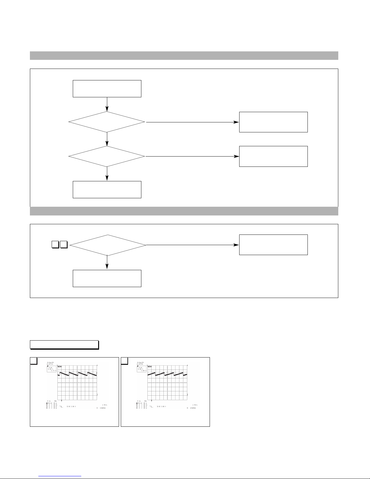
8 9
98
Q501 Emitter output varies
with different DAC values?
IC401 Pin 33, 34
output varies with different
DAC values?
IC401 Pin 26
output duty varies with
different DAC values?
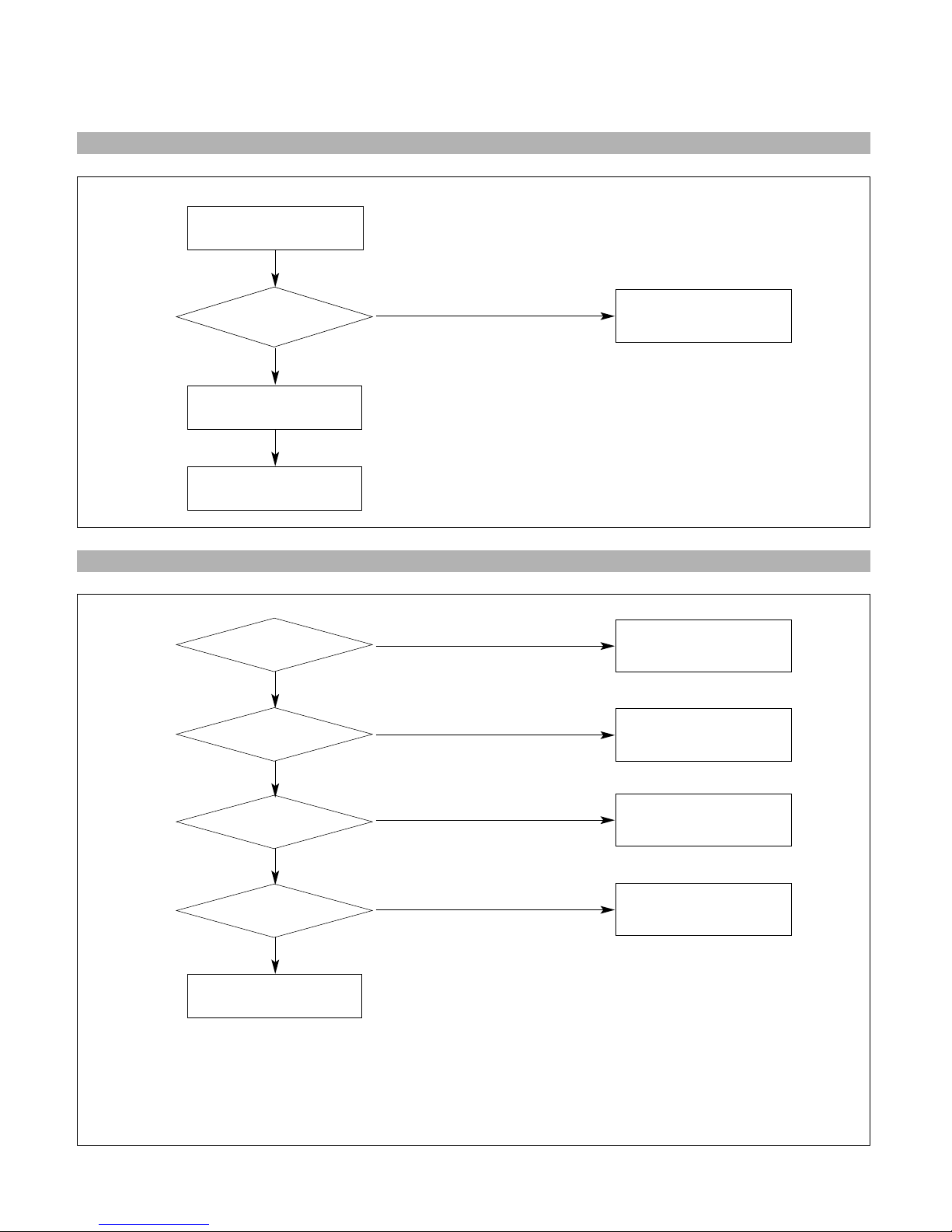
13. Tilt Failure
Check tilt connector
connection
Check and replace CRT.
NO
NO
Check and replace IC401.
Check Q503,Q501,Q502.
YES
YES
14. V Size or Pos. Variation Failure
Check and replace IC401
and IC601.
NO
Check some parts around IC401.
YES
- 27 -
IC401, #33 IC401, #34
Waveforms
Page 28
Q706 collecter waveform
is right?
15. High Voltage Failure
NO
NO
Replace T701
Check Q719,Q720
Check 50V line
Repeat the troubleshooting
Guide of H_deflection failure.
YES
YES
16. ABL Failure
YES
NO
Check and replace CRT
Input full white pattern to monitor.
Check P302, D801,
R801~803, R798.
Check and replace IC302
Check and replace T701
NO
YES
- 28 -
Q719, Drain Q706,Collector
IC302 Pin22
input exists and varies
with different patterns?
T701 Pin 6 Voltage exists?
18
18
Waveforms
21
21
YES
waveform is right?
Q719 drain
Page 29
22 23
Some parts around T701
are right?
IC401 Pin 24
output are right?
Q710 and parts around
are right?
17. Focus Failure
NO
NO
NO
Check the connection between
FBT Pin 12,
CRT Socket PCB.
Check and replace IC401.
Waveforms
Replace failed part.
Replace failed part.
YES
YES
YES
- 29 -
IC401, #24 FBT, #12
22
23
Page 30
3 4
43
IC401 Pin 23 input is
High Active?
All in/output values are
right?
IC401 Pin 45 and 46
inputs are right?
IC401 Pin 16 input is over
4.2V?
18. Micom Failure
19. OSD Failure
NO
NO
NO
NO
Done.
Change IC302
Check Q903,D908,ZD902
Check X401
Check and replace
R451,C408
Replace IC401.
YES
YES
YES
YES
- 30 -
IC401, #45
IC401, #46
Waveforms
Page 31
Proper Video levels are
on P301 Pin 1, 3 and 5.
IC401 Pins 27 and 28
inputs are right at
each function?
20. User Control Failure
Check connector Ass’y.
NO
Done.
Check and replace IC401.
Check and replace function key.
YES
21. Missing Color
NO
Change the CRT.
Check signal generator and
signal cable.
NO
Refer to 2 No Charcter.
NO
Check and replace IC303
and IC304
NO
Check C341, C346 and G2 wire.
Check around FBT circuits also.
YES
YES
YES
YES
- 31 -
Proper AC voltage are
on all cathodes?
Proper DC voltage are
on all cathodes?
G2 voltage is right?
Page 32
Blank pedestal is on
Pin 19, 20 and 21 of IC302
Is V_FLB and DC_bias on
G1 Pin at CRT socket?
G2 voltage is right?
22. Visible Retrace
Check white balance adjustment.
NO
NO
NO
Done.
Check G2 control volume and FBT.
Check IC302
and related components.
Check Q799
and related components.
YES
YES
YES
- 32 -
Degaussing circuit is right?
Purity is right?
23. Purity Failure
Degaussing
YES
NO
Replace CRT and verify purity.
Done.
Refer to 6 NO Degaussing.
NO
YES
Page 33
Improved focus?
Adjust Pole4,Pole6
to improve the misconvergence
24. Misconvergence
Degauss the CDT
Done.
Change CRT and readjust
convergence.
Yes
Done
No
25. Poor Focus
Adjust focus VR.
Check focus leads from
FBT to CRT Socket.
Check the CRT Socket.
YES
Aging monitor and
check for focus change.
NO
Refer to 18 Dynamic
Focus Failure.
NO
Replace the CRT and verify focus.
YES
- 33 -
Dynamic focus circuit is
right?
Page 34
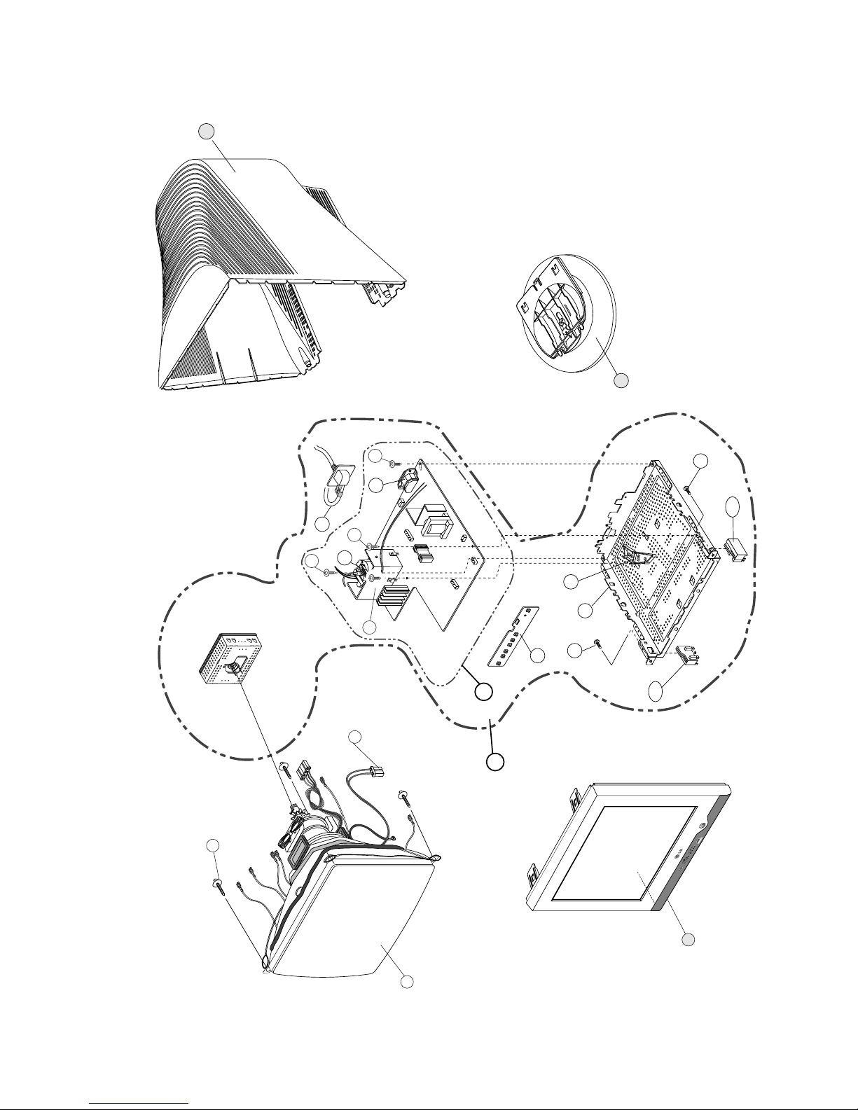
EXPLODED VIEW
- 34 -
10
13
12
13
11-2
11-1
4
3
7
B
A
2
6
6
5
9
8
a
b
c
b
1
M
E
N
U
S
E
LE
C
T
B
ri
g
h
t
v
i
e
w
Page 35

E XP L ODE D V IE W PA R TS L IS T
- 35 -
Des criptio n
C ABINE T AS S E MBLY , T 710B H B R AND C 079 5200H F ,T CO 99,B /VIE W ,E R 04, DI - F or W orld W ide (T 710B H)
C ABINE T AS S E MBLY , T 710S H B R AND C 079 320T (89483) , B /VIE W , L G R E D,DI(S P R IN G C KD) - F or Mexico, P ana ma (T 710S H)
C ABINE T AS S E MBLY , T 710S H B R AND C 079 320T ,89 483,B /VIE W,DI - F or T hailand (T 710S H)
C ABINE T AS S E MBLY , T 710B B R AND C 079 5008HF , B /VIE W, LAB E L C KD E R 04 - F or Is ra el (T 710B H)
C DT(C IR C), M41QE E 903X 01NHUD L G-P HIL IPS 85K HZ 29.1MM F LAT TC O H B - F or N orther n Hemis phe re
B AC K C OV E R AS S E MBLY , T 710B H/PH C046 G N5008H F , 8C 358(E Q5 4) - F or World W ide (T 710B H)
B AC K C OV E R AS S E MBLY , T 710 C 046 320T ,E Q54(8C 358) - F or Mex ic o, P anama , T hailand (T 710S H)
TILT S WIV E L AS S E MBLY , E 710B H T 066 B 60 HIP S
S CR E W AS S E MB LY , T AP TIT E P TY PE D5. 0 L25 .0 MS WR /F ZMY .
F B T ( F LY B AC K T R ANS FO R ME R ) C P2154/F700B K(17'')71K L INE C HANG E
S OC KE T(C IR C), P OWE R , C DT -3C DUO LING AC UNIV E R S AL 3P IN B LAC K
S OC KE T(C IR C), P OWE R , S A-4S H U A J IE AC U NIV ER S AL 3P IN B L AC K
C ABL E ,D-S UB , UL20276-9C (5. 8MM) AT 1560MM G R AY (8596 4) T 710B J DM
P W B( P CB ) A S S E MBLY ,S UB , T 710B K C ONT R OL T OT A L B R AND LG E N T
P W B( P CB ) A S S E MBLY ,S UB , T 710B HJ C ONT R O L T OT AL B R AND C A-131 - F or Is ra el
ME TAL, S HIE LD B OT TO M,C B553, 0.8T ,R E AR H O LE DE LE T E
ME TAL, S HIE LD B OT TO M C -CK D - F o r Is ra el
B R AC KE T , C N771C S UP P O R T ER B OT .(R IG HT )
B R AC KE T , C N771C S UP P O R T ER B OT .(LE FT )
S CR E W, P TP +4*20B P(MS WR /F ZMY )
B R AC KE T , C B77 7H H OLDE R F B T
MAIN T OT A L AS S E MB L Y , T 710B HK B R AND C A-131 L GE NT
P W B( P CB ) A S S E MBLY ,MAIN , T 710B HK K LR DE T B R AND C A-131 LG ENT
S CR E W, D R AW ING , D3. 5 L10.0 MS WR /F ZMY +S W3.5+R W 3.5
S CR E W AS S E MB LY , T AP TIT E P TY PE D3. 0 L10 .0 MS WR /F ZMY S W3+R W10
S CR E W, D R AW ING , P ZP +3*10(MS WR /FZMY )
P a r t N o.
3091T K C 089A
3091T K C 089U
3091T K C 089Y
3091T K C 089W
6318L17014A
3809T K C 050B
3809T K C 050C
3043T K K136A
339-002K
6174T 11005E
6620T K B002D
or 6620T KB 002B
6850T A 9012A
6871T S T 463B
6871T S T 377E
4950T K S 155S
4950T K S 212D
4810T K K150A
4810T K K151A
332-102F
4810T K K204A
3313T 17332B
6871T MT 496B
332-112F
4001T K K004E
332-095B
R ef. N o .
1
2
3
4
5
6
7
8
9
10
11-1
11-2
12
13
A
B
a
b
c
3091T K C 089L
3809T K C 050A
4950T K S 207A
C ABINE T AS S E MBLY , T 710B H B R AND C 079 5200H F ,T CO 99,B /VIE W ,E R 04
B AC K C OV E R AS S E MBLY , T 710B H/PH C046 G N5008H F , 8C 358(E Q5 4)
ME TAL, S HIE LD B OT TO M,C B553, 0.8T
Page 36
- 36 -
REPLACEMENT PARTS LIST
CAUTION: BEFORE REPLACING ANY OF THESE COMPONENTS,
READ CAREFULLY THE SAFETY PRECAUTIONS IN THIS MANUAL.
* NOTE : S SAFETY Mark
AL ALTERNATIVE PARTS
*S *AL LOC NO. PART NO. DESCRIPTION/SPECIFICATON
CAPACITORs
C301 0CQ1021N409 0.001UF D 100V 5% PE TP5
C302 0CE106CF638 Ò10UF SHL,SD 16V M FM5 TP 5Ó
C303 0CC5600K415 56P 50V J NP0 TP
C304 0CC5600K415 56P 50V J NP0 TP
C305 0CE476CF638 Ò47UF SHL,SD 16V M FM5 TP 5Ó
C306 0CZZTFT001M ECQB1H103JF3 MATSUSHITA 50V
10000PF 5% TAPING 103J
C307 0CC5600K415 56P 50V J NP0 TP
C308 0CK1020K515 1000PF 50V K B TR
C309 0CK1040K945 0.1UF 50V Z F TR
C311 0CK1040K945 0.1UF 50V Z F TR
C312 0CK1040K945 0.1UF 50V Z F TR
C313 0CK1040K945 0.1UF 50V Z F TR
C314 0CC4700W405 47PF 500V J SL TP
C315 0CE476EF638 47UF KMG 16V M FM5 TP 5
C316 0CK10202515 1000PF D 2KV 10% TR B(Y5P)
C317 0CK1040K945 0.1UF 50V Z F TR
C318 0CK1040K945 0.1UF 50V Z F TR
C319 0CK1040K945 0.1UF 50V Z F TR
C320 0CK10202515 1000PF D 2KV 10% TR B(Y5P)
C321 0CE225CK638 Ò2.2UF SHL,SD 50V M FM5 TP 5Ó
C323 0CE476CF638 Ò47UF SHL,SD 16V M FM5 TP 5Ó
C324 0CK1040K945 0.1UF 50V Z F TR
C325 181-288B MKT 100V 104JTR PHS26104
C326 0CC2200W415 22PF 500V J NP0 TR
C327 181-288B MKT 100V 104JTR PHS26104
C328 0CE226EN638 22UF KMG 100V M FM5 TP 5
C329 181-288B MKT 100V 104JTR PHS26104
C330 181-288B MKT 100V 104JTR PHS26104
C331 181-288G MKT 100V 334JTR PHS26334
C332 181-288G MKT 100V 334JTR PHS26334
C333 181-288G MKT 100V 334JTR PHS26334
C334 181-288B MKT 100V 104JTR PHS26104
C335 181-288B MKT 100V 104JTR PHS26104
C339 0CK1520W515 1500P 500V K B TS
C340 181-288B MKT 100V 104JTR PHS26104
C341 0CK10202515 1000PF D 2KV 10% TR B(Y5P)
C344 181-288B MKT 100V 104JTR PHS26104
C346 0CK10302940 0.01M 2KV Z F S
C372 0CK1040K945 0.1UF 50V Z F TR
C401 0CK1040K945 0.1UF 50V Z F TR
C404 0CK1040K945 0.1UF 50V Z F TR
C405 0CE107CF638 Ò100UF SHL,SD 16V M FM5 TP 5Ó
C406 0CK10102515 100PF D 2KV 10% B(Y5P) TR
C407 0CQ4721N409 0.0047UF D 100V 5% PE TP5
C408 0CK1040K945 0.1UF 50V Z F TR
C409 0CE106CF638 Ò10UF SHL,SD 16V M FM5 TP 5Ó
C410 0CK1010K515 100PF 50V K B TR
C411 0CK1010K515 100PF 50V K B TR
C412 0CK1020K515 1000PF 50V K B TR
C413 0CK1010K515 100PF 50V K B TR
C414 0CE106CF638 Ò10UF SHL,SD 16V M FM5 TP 5Ó
C415 0CK2220K515 2200P 50V K B TS
C416 0CQ1031N409 0.01U 100V J POLY TP
C417 0CK1040K945 0.1UF 50V Z F TR
C419 0CQ2221N409 2200PF 100V J PE TP
C420 0CQ6831N509 0.068U 100V K POLY TP
C421 0CK1020K515 1000PF 50V K B TR
C422 0CK2220K515 2200P 50V K B TS
C423 0CK2220K515 2200P 50V K B TS
C424 0CE475CK638 Ò4.7UF SHL,SD 50V M FM5 TP 5Ó
C426 0CK4710K515 470PF 50V K B TR
C427 0CK4710K515 470PF 50V K B TR
C501 0CE106CF638 Ò10UF SHL,SD 16V M FM5 TP 5Ó
C601 0CE227EF638 Ò220UF KMG,RD 16V 20% TP 5 FM5Ó
C602 181-288K MKT 100V 683JTR PHS26683
C603 0CE107EK638 100UF KMG 50V M FM5 TP 5
C604 0CZZTFT001V ECQB1H473JM3 473J 50V TP5.0
MATSUSHITA
C605 0CK1020W515 1000P 500V K B TS
C701 0CK1040K945 0.1UF 50V Z F TR
C712 0CK1040K945 0.1UF 50V Z F TR
C713 0CK2210K515 220P 50V K B TS
C714 0CE107CH638 Ò100UF SHL,SD 25V M FM5 TP 5Ó
C715 181-288N MKT 100V 103JTR PHS86103
C719 0CZZTAB001F SHL-BP SYE / SWE 50V 3.3UF 20% BULK
EB770H
C720 0CK10201515 1000P 1KV K B TS
C722 181-303E 224J 30.0*19.5*12.0*20.0 250V J PU FM20
C723 181-305B 124J 19.0*13.5*7.5*10.0 250V J MPP FM10
C724 0CK1040K945 0.1UF 50V Z F TR
C726 181-305F MPP 250V 274J S=10.0
C727 0CK1040K945 0.1UF 50V Z F TR
C729 181-305L 684J 26.0*19.0*12.5*15.0 250V
J MPP FM15
C730 0CK1040K945 0.1UF 50V Z F TR
C731 0CBZTBU004H 5600PF D 2.5KV H M/PP NI FM20
C733 0CBZTBU003H 362J 20.0*12.0*7.0*10.0 800V J BUP FM10
C738 181-302M 822J 19.5*12.0*7.0*10.0 250V J PU FM10
C739-1 0CE106CN638 Ò10UF SHL,SD 100V M FM5 TP 5Ó
C740 0CE227EL630 220UF KMG 63V M FM5 BULK
C741 0CZZTFT002B ECQV1H154JZ3 154J 50V TP5.0
MATSUSHITA
C744 181-305L 684J 26.0*19.0*12.5*15.0 250V
J MPP FM15
C745 0CK5610W515 560P 500V K B TS
C748 0CK1510W515 150PF 500V K B TR
C749 0CE4756Q638 4.7000UF SMS 200V M FM5 TP5
C750 0CK1040K945 0.1UF 50V Z F TR
C756 0CK4700K515 47PF D 50V 10% B(Y5P) TR
C767 0CK10301945 10000PF D 1KV Z F(Y5V) TR
C801 0CK1040K945 0.1UF 50V Z F TR
C901 0CZZTFB001B BULK MPX 474K2YL (X2) BULK 22.5
C902 0CZZTFB001C ÒMPX104K2YL ETR 275V 0.1UF
10%,-10% BULK X2Ó
C903 0CZZTCB003D BULK 7.5 CS E 102M 8.0 250V TDK
C904 0CZZTCB003A BULK 7.5 CS E 222M 10.5 250V TDK
C905 0CZZTCB003A BULK 7.5 CS E 222M 10.5 250V TDK
C906 0CZZTCB003D BULK 7.5 CS E 102M 8.0 250V TDK
C907 0CKZTBU003C SC E 472M 14.0BW7 250V BK7.5
SAMWHA Y2
C908 0CEZTBU002D 180UF 25.4*35 SMH/HC 400V M
VNSN BULK
C909 0CK10301945 10000PF D 1KV Z F(Y5V) TR
C910 0CK22101515 220P 1KV K B TP5
C911 0CE475CK638 Ò4.7UF SHL,SD 50V M FM5 TP 5Ó
*S *AL LOC NO. PART NO. DESCRIPTION/SPECIFICATON
DATE:2004.08.08
DATE:2004.08.08
Page 37
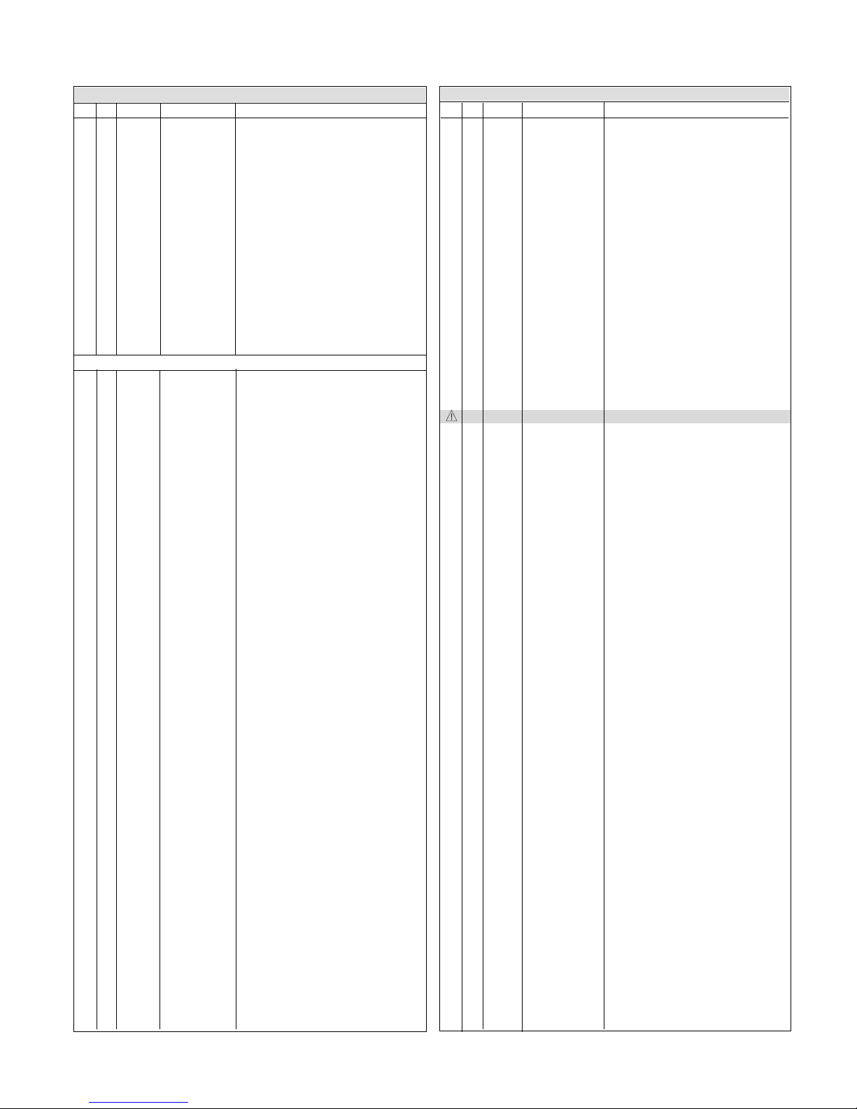
*S *AL LOC NO. PART NO. DESCRIPTION/SPECIFICATON
DATE:2004.08.08
C912 0CK3310K515 330P 50V K B TS
C913 0CE476CK638 Ò47UF SHL,SD 50V M FM5 TP 5Ó
C914 0CZZTFT001P ECQB1H153JM3 153J 50V TP5.0
MATSUSHITA
C915 0CK6810K515 680P 50V K B TS
C917 0CK1020K515 1000PF 50V K B TR
C918 0CK1040K945 0.1UF 50V Z F TR
C921 0CZZTCB003A BULK 7.5 CS E 222M 10.5 250V TDK
C941 0CE108CD618 1000UF SHL 10V M FL TP5
C942 0CE107CF638 Ò100UF SHL,SD 16V M FM5 TP 5Ó
C943 0CK56101515 560P 1KV K B TS
C951 0CE108CF630 1000UF SHL 16V M FM5 BULK
C952 0CE107CF638 Ò100UF SHL,SD 16V M FM5 TP 5Ó
C953 0CE107CF638 Ò100UF SHL,SD 16V M FM5 TP 5Ó
C954 0CE108CD618 1000UF SHL 10V M FL TP5
C971 0CE476EK638 47UF KMG 50V M FM5 TP 5
C998 0CE227EL630 220UF KMG 63V M FM5 BULK
DIODEs
D301 0DSPT00029A 1N4148M PCTRONIX TP DO34 100V 75VA
2000MA 4NSEC 0.025UA
D302 0DSPT00029A 1N4148M PCTRONIX TP DO34 100V 75VA
2000MA 4NSEC 0.025UA
D303 0DSPT00029A 1N4148M PCTRONIX TP DO34 100V 75VA
2000MA 4NSEC 0.025UA
D304 0DSPT00029A 1N4148M PCTRONIX TP DO34 100V 75VA
2000MA 4NSEC 0.025UA
D305 0DSPT00029A 1N4148M PCTRONIX TP DO34 100V 75VA
2000MA 4NSEC 0.025UA
D306 0DSPT00029A 1N4148M PCTRONIX TP DO34 100V 75VA
2000MA 4NSEC 0.025UA
D307 0DSPT00029A 1N4148M PCTRONIX TP DO34 100V 75VA
2000MA 4NSEC 0.025UA
D308 0DSPT00029A 1N4148M PCTRONIX TP DO34 100V 75VA
2000MA 4NSEC 0.025UA
D309 0DSPT00029A 1N4148M PCTRONIX TP DO34 100V 75VA
2000MA 4NSEC 0.025UA
D310 0DSPT00019A PSS244 PCTRONIX TP DO34 280V 625MA
1000MA 50NSSEC 10UA
D311 0DSPT00019A PSS244 PCTRONIX TP DO34 280V 625MA
1000MA 50NSSEC 10UA
D312 0DSPT00019A PSS244 PCTRONIX TP DO34 280V 625MA
1000MA 50NSSEC 10UA
D313 0DSPT00019A PSS244 PCTRONIX TP DO34 280V 625MA
1000MA 50NSSEC 10UA
D314 0DSPT00019A PSS244 PCTRONIX TP DO34 280V 625MA
1000MA 50NSSEC 10UA
D315 0DSPT00019A PSS244 PCTRONIX TP DO34 280V 625MA
1000MA 50NSSEC 10UA
D316 0DRTW00119A 1N4005-1021 TIWAN SEMI TP DO41 600V
1A 30A 2USSEC 5.0UA
D401 0DSPT00029A 1N4148M PCTRONIX TP DO34 100V 75VA
2000MA 4NSEC 0.025UA
D402 0DSPT00029A 1N4148M PCTRONIX TP DO34 100V 75VA
2000MA 4NSEC 0.025UA
D403 0DSPT00029A 1N4148M PCTRONIX TP DO34 100V 75VA
2000MA 4NSEC 0.025UA
D406 0DSPT00019A PSS244 PCTRONIX TP DO34 280V 625MA
1000MA 50NSSEC 10UA
D407 0DSPT00029A 1N4148M PCTRONIX TP DO34 100V 75VA
2000MA 4NSEC 0.025UA
D501 0DSPT00029A 1N4148M PCTRONIX TP DO34 100V 75VA
2000MA 4NSEC 0.025UA
D703 0DRGF00120A MUR460(15MM) GULF BK DO201AD 600V
4A 150A 45NSSEC 10UA
D704 0DRFC00300A FFPF04U150S FAIR CHILD BK TO220F
1500V 4A 40A 150NSSEC 7UA
D705 0DRTW00089A SRT14(1021) TIWAN SEMI TP NON 40V 1A
25A .SEC 0.5MA
D706 0DRFC00300A FFPF04U150S FAIR CHILD BK TO220F
1500V 4A 40A 150NSSEC 7UA
D710 0DR400409AC UF4004 GULF TP DO41 400V 1A 30A
50NSEC 10UA
D712 0DR100009CD RGP10G-1021 TIWAN SEMI TP DO41 400V
1A 30A 150NSEC 5UA
D714 0DSPT00029A 1N4148M PCTRONIX TP DO34 100V 75VA
2000MA 4NSEC 0.025UA
D715 0DSPT00029A 1N4148M PCTRONIX TP DO34 100V 75VA
2000MA 4NSEC 0.025UA
D716 0DRTW00119A 1N4005-1021 TIWAN SEMI TP DO41 600V
1A 30A 2USSEC 5.0UA
D717 0DRTW00119A 1N4005-1021 TIWAN SEMI TP DO41 600V
1A 30A 2USSEC 5.0UA
D718 0DRTW00119A 1N4005-1021 TIWAN SEMI TP DO41 600V
1A 30A 2USSEC 5.0UA
D719 0DR100009DC RGP10J-1021 TIWAN SEMI TP DO41 600V
1A 30A 250NSEC 5UA
D721 0DR100009CD RGP10G-1021 TIWAN SEMI TP DO41 400V
1A 30A 150NSEC 5UA
D723 0DSPT00029A 1N4148M PCTRONIX TP DO34 100V 75VA
2000MA 4NSEC 0.025UA
D768 0DD400709CC UF4007-1021 TIWAN SEMI TP DO204AL
1000V 1A 30A 75NSEC 10UA
D801 0DSPT00029A 1N4148M PCTRONIX TP DO34 100V 75VA
2000MA 4NSEC 0.025UA
D900 0DRTW00121A D2SB60-1121 TIWAN SEMI ST GBL 600V
2A 80A _SEC 10UA
D902 0DRGF00139A GPP20J GULF TP DO15 600V 2.0A 70A
2.0USSEC 5.0UA
D904 0DR100009CD RGP10G-1021 TIWAN SEMI TP DO41 400V
1A 30A 150NSEC 5UA
D905 0DD400709CC UF4007-1021 TIWAN SEMI TP DO204AL
1000V 1A 30A 75NSEC 10UA
D906 0DR100009CD RGP10G-1021 TIWAN SEMI TP DO41 400V
1A 30A 150NSEC 5UA
D908 0DSPT00029A 1N4148M PCTRONIX TP DO34 100V 75VA
2000MA 4NSEC 0.025UA
D910 0DSPT00029A 1N4148M PCTRONIX TP DO34 100V 75VA
2000MA 4NSEC 0.025UA
D911 0DSPT00029A 1N4148M PCTRONIX TP DO34 100V 75VA
2000MA 4NSEC 0.025UA
D941 0DR400409AC UF4004 GULF TP DO41 400V 1A 30A
50NSEC 10UA
D942 0DR400409AC UF4004 GULF TP DO41 400V 1A 30A
50NSEC 10UA
D951 0DRGF00150A UF5404 GULF BK DO201AD 400V 3.0A
150A 50NSSEC 10.0UA
D952 0DSPT00029A 1N4148M PCTRONIX TP DO34 100V 75VA
2000MA 4NSEC 0.025UA
D961 0DRGS00090A 31GF6L-5701 GENERAL
SEMICONDUCTOR BK NON 600V 3A 60A
30NSEC 20UA
D971 0DD400709CC UF4007-1021 TIWAN SEMI TP DO204AL
1000V 1A 30A 75NSEC 10UA
ZD301 0DZPT43009A UZ-4.3BSB PCTRONIX TP DO34 500MW
4.3BV 5MA (52MMTP)PF
ZD402 0DZPT56009A UZ-5.6BSB PCTRONIX TP52 DO34 500MW
5.6BV 5MA PF
ZD403 0DZPT56009A UZ-5.6BSB PCTRONIX TP52 DO34 500MW
5.6BV 5MA PF
ZD404 0DZPT56009A UZ-5.6BSB PCTRONIX TP52 DO34 500MW
- 37-
*S *AL LOC NO. PART NO. DESCRIPTION/SPECIFICATON
DATE:2004.08.08
Page 38
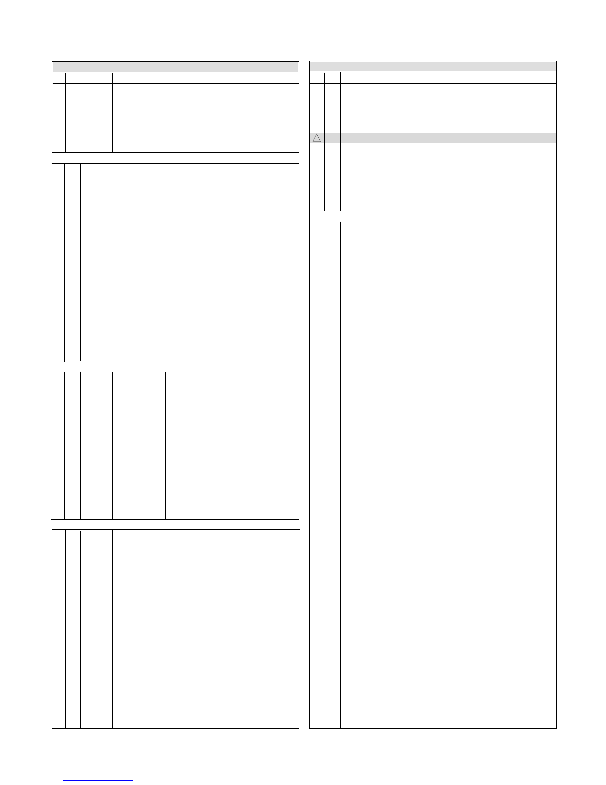
DATE:2004.08.08
DATE:2004.08.08
5.6BV 5MA PF
ZD405 0DZPT56009A UZ-5.6BSB PCTRONIX TP52 DO34 500MW
5.6BV 5MA PF
ZD406 0DZPT56009A UZ-5.6BSB PCTRONIX TP52 DO34 500MW
5.6BV 5MA PF
ZD902 0DZPT51009A UZ-5.1BSB PCTRONIX TP DO34 500MW
5.1BV 5MA PF
COILs&COREs
FB302 6210TCE003L BAS3580T BO SUNG 3580MM AXIAL52MM
FB305 6210TCE003P BRS2550B BO SUNG 2550MM RADIAL
FB306 6210TCE003L BAS3580T BO SUNG 3580MM AXIAL52MM
FB307 6210TCE003B BRS3580B BO SUNG 3580MM RADIAL
FB308 6210TCE003J BAS2550T BO SUNG 2550MM AXIAL52MM
FB309 6210TCE003J BAS2550T BO SUNG 2550MM AXIAL52MM
FB310 6210TCE003A BRD3510B BO SUNG 3510MM RADIAL
FB313 6210TCE003J BAS2550T BO SUNG 2550MM AXIAL52MM
FB701 6210TCE003L BAS3580T BO SUNG 3580MM AXIAL52MM
FB903 6210TCE003P BRS2550B BO SUNG 2550MM RADIAL
FB905 6210TCE003J BAS2550T BO SUNG 2550MM AXIAL52MM
FB906 6210TCE003P BRS2550B BO SUNG 2550MM RADIAL
FB921 6210TCE003A BRD3510B BO SUNG 3510MM RADIAL
FB922 6210TCE003A BRD3510B BO SUNG 3510MM RADIAL
L903 6210TCE003K BAS3550T BO SUNG 3550MM AXIAL52MM
L702 6140TBZ025D Ò- - H-SIZE,DR12*20-C6.0,150UH 700BJÓ
L703 6140TYZ013A ÒLX31 SAMHWA DR14*15-C5.2,
17.5T,5.6UH TÓ
L705 6140TBZ026C DR15*18-C9.8 100UH 0.1*30MM 40.5T D/D
CHOKE
Ics
IC302 0IPRPNS025C ÒLM1246DDC/NA NATIONAL
SEMICONDUCTOR 24,DIP ST ONE CHIP
(VIDEO+OSD)Ó
IC303 0IPRPNS050A LM2470TA NATIONAL SEMICONDUCTOR
9PIN TA09A ST MONOLITHIC TRIPLE
7.0NS CRT DRIVER
IC304 0IPRPNS005A ÒLM2480NA NATIONAL SEMICONDUCTOR
8P,DIP ST 80V TRIPLE BIAS CLAMPÓ
IC401 0IMCRPH033A SAA4849(OTP) PHILIPS 56PIN SDIP -
DEFLECTION AND MICOM
IC402 0IMMRSG044A M24C08-WBN6 STM 8PIN PDIP ST SERIAL
IIC EEPROM
IC601 0IPRPPH018A ÒTDA4867J PHILIPS 9PIN,ST DIP
VERTICAL OUTPUT ICÓ
IC901 0ISS384200A KA3842B (PWM)
TRANSISTORs
Q501 0TR320209AA KTC3202-Y(KTC1959) TP KEC TO92 NPN
Q502 0TR127009AA KTA1270-Y(KTA562TM) TP KEC TO92 PNP
Q503 0TR319809AA KTC3198-Y(KTC1815) TP KEC TO92 NPN
Q703 0TFFC10012A FQPF10N20C FAIRCHILD ST TO220F
200V 9.5A
Q704 0TR390409CA FAIRCHILD 2N3904(TA) TP TO-92
60V 0.2A
Q705 0TR200009AB KTC200-Y TP KEC TO92 NPN
Q706 0TRFC10008A FJAF5804(TU) FAIRCHILD ST TO3PF
1500V 12A
Q710 0TRKE90020A MPSA44 KEC TP TO92 500V 300MA
Q711 0TF630001BB SGS-T(STM) IRF630MFP ST TO220F
200V 5A
Q712 0TF630001BB SGS-T(STM) IRF630MFP ST TO220F
200V 5A
Q713 0TF630001BB SGS-T(STM) IRF630MFP ST TO220F
200V 5A
Q714 0TR319809AA KTC3198-Y(KTC1815) TP KEC TO92 NPN
Q715 0TR319809AA KTC3198-Y(KTC1815) TP KEC TO92 NPN
Q716 0TR319809AA KTC3198-Y(KTC1815) TP KEC TO92 NPN
Q719 0TFFC10012A FQPF10N20C FAIRCHILD ST TO220F
200V 9.5A
Q720 0TR390409CA FAIRCHILD 2N3904(TA) TP TO-92
60V 0.2A
Q799 0TRKE90019A MPSA92 KEC TP TO92 -300V -500MA
Q901 0TF760000AD SSS7N60B FAIRCHILD ST TO220F
650V 7A
Q903 0TR100809AA KSC1008C-Y TP SAMSUNG TO92 NPN
Q941 0TR319809AA KTC3198-Y(KTC1815) TP KEC TO92 NPN
Q942 0TR127309AA KTA1273-Y(KTA966A) TP KEC TO92L PNP
Q951 0TR319809AA KTC3198-Y(KTC1815) TP KEC TO92 NPN
Q952 0TR127309AA KTA1273-Y(KTA966A) TP KEC TO92L PNP
Q953 0TR319809AA KTC3198-Y(KTC1815) TP KEC TO92 NPN
RESISTORs
R201 0RD1001Q609 1K 1/4W(3 5% TA52
R202 0RD0912Q609 91 OHM 1/4 W (3.4) 5% TA52
R203 0RD2200Q609 220 1/4W(3 5% TA52
R204 0RD4300Q609 430 OHM 1/4 W(3.4) 5.00% TA52
R205 0RD1001Q609 1K 1/4W(3 5% TA52
R206 0RD0912Q609 91 OHM 1/4 W (3.4) 5% TA52
R207 0RD4300Q609 430 OHM 1/4 W(3.4) 5.00% TA52
R208 0RD2200Q609 220 1/4W(3 5% TA52
R209 0RD9100Q609 910 1/4W(3 5% TA52
R211 0RD2200Q609 220 1/4W(3 5% TA52
R301 0RD0752Q609 75 1/4W(3 5% TA52
R302 0RD0752Q609 75 1/4W(3 5% TA52
R303 0RD0752Q609 75 1/4W(3 5% TA52
R305 0RN6201F409 6.20K 1/6W 1% TA52
R314 0RD1000Q609 100 1/4W(3 5% TA52
R315 0RD1000Q609 100 1/4W(3 5% TA52
R319 0RD4701Q609 4.70K 1/4W(3 5% TA52
R320 0RD4701Q609 4.70K 1/4W(3 5% TA52
R326 0RD2201Q609 2.20K 1/4W(3 5% TA52
R327 0RD1001Q609 1K 1/4W(3 5% TA52
R328 0RD1001Q609 1K 1/4W(3 5% TA52
R329 0RD1001Q609 1K 1/4W(3 5% TA52
R330 0RD1001Q609 1K 1/4W(3 5% TA52
R331 0RD1600Q609 160 1/4W(3 5% TA52
R332 0RD1600Q609 160 1/4W(3 5% TA52
R333 0RD1300Q609 130 1/4W(3 5% TA52
R334 0RD3303Q609 330K 1/4W(3 5% TA52
R335 0RD3303Q609 330K 1/4W(3 5% TA52
R336 0RD3303Q609 330K 1/4W(3 5% TA52
R337 0RD1000Q609 100 1/4W(3 5% TA52
R338 0RD0102Q609 10 1/4W(3 5% TA52
R340 0RN1002F409 10K 1/6W 1 TA52
R341 0RD0332A609 33 OHM 1/2 W (7.0) 5% TA52
R342 0RD0332A609 33 OHM 1/2 W (7.0) 5% TA52
R343 0RD0332A609 33 OHM 1/2 W (7.0) 5% TA52
R344 0RD0332Q609 33 1/4W(3 5% TA52
R345 0RD0332Q609 33 1/4W(3 5% TA52
R346 0RD0332Q609 33 1/4W(3 5% TA52
R347 0RD0202Q609 20 1/4W(3 5% TA52
R401 0RD2200Q609 220 1/4W(3 5% TA52
R402 0RD1000Q609 100 1/4W(3 5% TA52
R403 0RD1000Q609 100 1/4W(3 5% TA52
R404 0RD1000Q609 100 1/4W(3 5% TA52
R405 0RD2201Q609 2.20K 1/4W(3 5% TA52
R406 0RD2201Q609 2.20K 1/4W(3 5% TA52
R407 0RD4701Q609 4.70K 1/4W(3 5% TA52
R408 0RD1000Q609 100 1/4W(3 5% TA52
R409 0RD1000Q609 100 1/4W(3 5% TA52
R411 0RD1000Q609 100 1/4W(3 5% TA52
R412 0RD1000Q609 100 1/4W(3 5% TA52
R413 0RD1000Q609 100 1/4W(3 5% TA52
*S *AL LOC NO. PART NO. DESCRIPTION/SPECIFICATON
- 38 -
*S *AL LOC NO. PART NO. DESCRIPTION/SPECIFICATON
Page 39
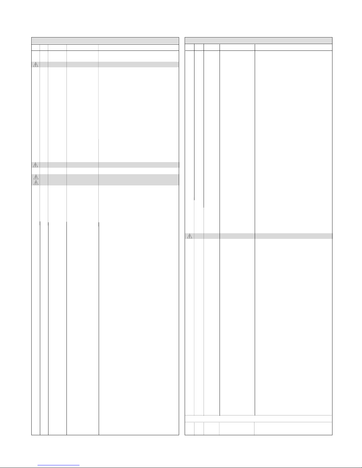
DATE:2004.08.08 DATE:2004.08.08
R414 0RD1602Q609 16K 1/4W(3 5% TA52
R415 0RD1000Q609 100 1/4W(3 5% TA52
R416 0RN1501F409 1.5K 1/6W 1 TA52
R417 0RD1000Q609 100 1/4W(3 5% TA52
R419 0RN4702F409 47K 1/6W 1% TA52
R420 0RD2001Q609 2K 1/4W(3 5% TA52
R421 0RD1501Q609 1.50K 1/4W(3 5% TA52
R422 0RD2001Q609 2K 1/4W(3 5% TA52
R423 0RD1000Q609 100 1/4W(3 5% TA52
R424 0RD1000Q609 100 1/4W(3 5% TA52
R425 0RD1000Q609 100 1/4W(3 5% TA52
R426 0RD1000Q609 100 1/4W(3 5% TA52
R427 0RD1002Q609 10K 1/4W(3 5% TA52
R429 0RD1002Q609 10K 1/4W(3 5% TA52
R430 0RD1000Q609 100 1/4W(3 5% TA52
R431 0RD1802Q609 18K 1/4W(3 5% TA52
R432 0RD2001Q609 2K 1/4W(3 5% TA52
R434 0RD1503Q609 150K 1/4W(3 5% TA52
R436 0RD3601Q609 3.60K 1/4W(3 5% TA52
R437 0RN2702F409 27K 1/6W 1% TA52
R438 0RD1303Q609 130K 1/4W(3 5% TA52
R439 0RN4700F409 470 1/6W 1 TA52
R440 0RN1001F409 1K 1/6W 1% TA52
R441 0RD6802Q609 68K 1/4W(3 5% TA52
R442 0RN3901F409 3.90K 1/6W 1% TA52
R443 0RD2200Q609 220 1/4W(3 5% TA52
R444 0RD4700Q609 470 OHM 1/4 W (3.4) 5% TA52
R445 0RD4700Q609 470 OHM 1/4 W (3.4) 5% TA52
R446 0RD1000Q609 100 1/4W(3 5% TA52
R447 0RD1000Q609 100 1/4W(3 5% TA52
R449 0RN7501F409 7.50K 1/6W 1% TA52
R450 0RD1203Q509 120K OHM 1/4 W (3.4) 2% TA52
R451 0RD1001Q609 1K 1/4W(3 5% TA52
R452 0RD2002Q609 20K 1/4W(3 5% TA52 (T710BHL)
R453 0RD2001Q609 2K 1/4W(3 5% TA52
R454 0RD2001Q609 2K 1/4W(3 5% TA52
R455 0RD1002Q609 10K 1/4W(3 5% TA52
R456 0RD1000Q609 100 1/4W(3 5% TA52
R461 0RD3900Q609 390 1/4W(3 5% TA52
R462 0RD2001Q609 2K 1/4W(3 5% TA52
R463 0RD4701Q609 4.70K 1/4W(3 5% TA52
R464 0RD3001Q609 3K 1/4W(3 5% TA52
R501 0RD0102A609 10 OHM 1/2 W (7.0) 5% TA52
R502 0RD8202Q609 82K 1/4W(3 5% TA52
R503 0RD1502Q609 15K 1/4W(3 5% TA52
R598 0RD2001Q609 2K 1/4W(3 5% TA52
R601 0RD1000Q609 100 1/4W(3 5% TA52
R602 0RD1000Q609 100 1/4W(3 5% TA52
R603 0RN0220H609 0.22 1/2W 5% TA52
R604 0RD0101A609 1 OHM 1/2 W (7.0) 5% TA52
R605 0RD0102A609 10 OHM 1/2 W (7.0) 5% TA52
R606 0RD4700Q609 470 OHM 1/4 W (3.4) 5% TA52
R607 0RN4301F409 4.30K 1/6W 1% TA52
R608 0RD5600A609 560 OHM 1/2 W (7.0) 5% TA52
R701 0RD4700Q609 470 OHM 1/4 W (3.4) 5% TA52
R702 0RD6200Q609 620 1/4W(3 5% TA52
R703 0RD5601Q609 5.60K 1/4W(3 5% TA52
R704 0RD1002Q609 10K 1/4W(3 5% TA52
R705 0RD0102Q609 10 1/4W(3 5% TA52
R706 0RD3302A609 33K OHM 1/2 W (7.0) 5% TA52
R727 0RX0272K665 27 OHM 2 W 5% SF
R728 0RD1001Q609 1K 1/4W(3 5% TA52
R729 0RD1002Q609 10K 1/4W(3 5% TA52
R736 0RX2201J609 2.2KOHM 1 W 5% TA52
R739 0RD2701Q609 2.70K 1/4W(3 5% TA52
R740 0RD0271A609 2.7 OHM 1/2 W (7.0) 5% TA52
R744 0RD1001A609 1K OHM 1/2 W (7.0) 5% TA52
R745 0RD4702Q609 47K 1/4W(3 5% TA52
R746 0RD2201Q609 2.20K 1/4W(3 5% TA52
R747 0RD3001Q609 3K 1/4W(3 5% TA52
R748 0RD4702Q609 47K 1/4W(3 5% TA52
R749 0RD2201Q609 2.20K 1/4W(3 5% TA52
R750 0RD3001Q609 3K 1/4W(3 5% TA52
R751 0RD0222A609 22 OHM 1/2 W (7.0) 5% TA52
R752 0RD2201Q609 2.20K 1/4W(3 5% TA52
R753 0RD3001Q609 3K 1/4W(3 5% TA52
R754 0RD6800A609 680 OHM 1/2 W (7.0) 5% TA52
R756 0RD2202A609 22K OHM 1/2 W (7.0) 5% TA52
R761 0RD3001Q609 3K 1/4W(3 5% TA52
R762 0RD3001Q609 3K 1/4W(3 5% TA52
R763 0RD3001Q609 3K 1/4W(3 5% TA52
R765 0RD3000A609 300 OHM 1/2 W (7.0) 5% TA52
R768 0RD4703A609 470K OHM 1/2 W (7.0) 5% TA52
R771 0RD3001Q609 3K 1/4W(3 5% TA52
R772 0RD1202Q509 12K OHM 1/4 W (3.4) 2% TA52
R773 0RD6202A609 62K OHM 1/2 W (7.0) 5% TA52
R782 0RD3301A609 3.3K OHM 1/2 W(7.0) 5.00% TA52
R793 0RD4702Q609 47K 1/4W(3 5% TA52
R797 0RD1501Q609 1.50K 1/4W(3 5% TA52
R798 0RD2001Q609 2K 1/4W(3 5% TA52
R799 0RD1502Q609 15K 1/4W(3 5% TA52
R801 0RD1502Q609 15K 1/4W(3 5% TA52
R802 0RD1502Q609 15K 1/4W(3 5% TA52
R803 0RD1001Q609 1K 1/4W(3 5% TA52
R809 0RX0101K665 1 OHM 2 W 5% SF
R818 0RN6202F409 62KOHM 1/6 W 1% TA52
R901 0RD4703A609 470K OHM 1/2 W (7.0) 5% TA52
R902 0RD0332Q609 33 1/4W(3 5% TA52
R903 0RN0562F409 56 OHM 1/6 W 1% TA52
R904 0RX3902K665 39K OHM 2 W 5% SF
R906 0RD6200Q609 620 1/4W(3 5% TA52
R907 0RD3902Q609 39K 1/4W(3 5% TA52
R910 0RX4702J609 47K OHM 1 W 5% TA52
R911 0RD0202Q609 20 1/4W(3 5% TA52
R912 0RN1802F409 18K 1/6W 1% TA52
R913 0RN2701F409 2.7K OHM 1/6 W 1.00% TA52
R915 0RD2000Q609 200 1/4W(3 5% TA52
R916 0RD1002Q609 10K 1/4W(3 5% TA52
R918 0RD1001Q609 1K 1/4W(3 5% TA52
R923 0RD1003Q609 100K 1/4W(3 5% TA52
R924 0RN0390H609 0.39 1/2W 5 TA52
R925 0RN0390H609 0.39 1/2W 5 TA52
R926 0RD4301Q609 4.30K 1/4W(3 5% TA52
R927 0RD2002Q609 20K 1/4W(3 5% TA52
R928 0RD1800Q609 180 1/4W(3 5% TA52
R929 0RD0332Q609 33 1/4W(3 5% TA52
R941 0RN0220H609 0.22 1/2W 5% TA52
R944 0RD4700A609 470 OHM 1/2 W (7.0) 5% TA52
R945 0RD4701Q609 4.70K 1/4W(3 5% TA52
R952 0RD1202A609 12K OHM 1/2 W(7.0) 5.00% TA52
R953 0RD1001A609 1K OHM 1/2 W (7.0) 5% TA52
R954 0RD4701Q609 4.70K 1/4W(3 5% TA52
R955 0RD4701Q609 4.70K 1/4W(3 5% TA52
R956 0RD6802A609 68K OHM 1/2 W (7.0) 5% TA52
R957 0RD0472A609 47 OHM 1/2 W (7.0) 5% TA52
R960 0RD6200A609 620 OHM 1/2 W(7.0) 5.00% TA52
OTHERs
RL901 6920TBB007A JZC-42012-2HS HONGMEI 250VAC 5A 12V
2A NO VENTING
- 39 -
*S *AL LOC NO. PART NO. DESCRIPTION/SPECIFICATON
*S *AL LOC NO. PART NO. DESCRIPTION/SPECIFICATON
R452 0RD6201Q609
6.20K 1/4W (3 5% TA52 (T710BL)
Page 40
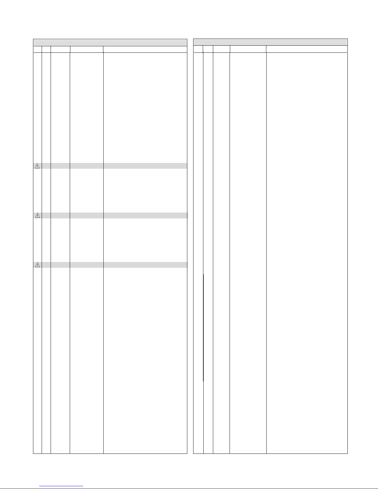
DATE:2004.08.08
DATE:2004.08.08
SG305 6918TRT005A ÒSSG-102-A0,1KV SMART RADIAL
TAPINGÓ
SG701 6918TRT005A ÒSSG-102-A0,1KV SMART RADIAL
TAPINGÓ
SW201 6600R00001A ÒJTP1280F6 JEIL 12V DC 1MA
VERTICAL,7MMÓ
SW202 6600R00001A ÒJTP1280F6 JEIL 12V DC 1MA
VERTICAL,7MMÓ
SW203 6600R00001A ÒJTP1280F6 JEIL 12V DC 1MA
VERTICAL,7MMÓ
SW204 6600R00001A ÒJTP1280F6 JEIL 12V DC 1MA
VERTICAL,7MMÓ
SW205 6600R00001A ÒJTP1280F6 JEIL 12V DC 1MA
VERTICAL,7MMÓ
SW206 6600R00001A ÒJTP1280F6 JEIL 12V DC 1MA
VERTICAL,7MMÓ
SW207 6600R00001A ÒJTP1280F6 JEIL 12V DC 1MA
VERTICAL,7MMÓ
T701 6174T11004F Ò1063A,F700BK(71K) JUNGWOO 17ÓÓÓ
TH901 6322B00002D MZ72-4.5RN290V GAOLI 4.5OHM +30% -
20% 2PIN BOX
TH902 6322A00003C 8 D2 10 SEMITEC 8OHM 15% D(11.5)
X401 6212AA2003E HC-49U SOUTH STAR 48MHZ +/- 20 PPM
22PF BULK
F1 430-858C AFC-520 BAE EUN TA
F2 430-858C AFC-520 BAE EUN TA
F901 0FZZTTH001B ÒTIME LAG HBC 5A/250V,215
005,LITTELFUSEÓ
FB301 6210TCZ001J BAS3550T0(125-022J) BO SUNG
RH3.5*5.0*0.8TMM AXIAL52MM
FB303 6210TCZ001J BAS3550T0(125-022J) BO SUNG
RH3.5*5.0*0.8TMM AXIAL52MM
FB304 6210TCZ001J BAS3550T0(125-022J) BO SUNG
RH3.5*5.0*0.8TMM AXIAL52MM
L901 6200TZZ004A ÒSQE2626 NAMYANG BK L/FILTER
15MH,EB770HÓ
- 40 -
*S *AL LOC NO. PART NO. DESCRIPTION/SPECIFICATON
*S *AL LOC NO. PART NO. DESCRIPTION/SPECIFICATON
Page 41
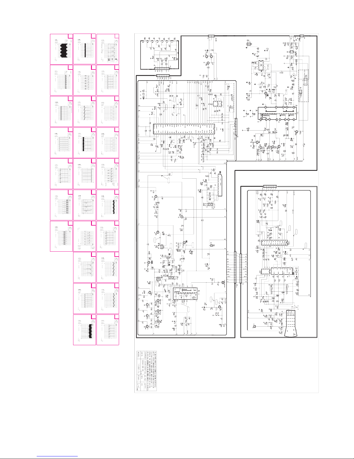
- 42 -
- 43 -
S CHE MAT IC DIA GR A M
NO TIC E
S ince this is a ba sic sche matic diagra m.
The value of compone nts a nd some partial connection a re
suc ject to be changed for improveme nt without notice.
01
01
23
01 01 01
26
01
27
01
28
01
29 3 0 3 1
01 01
14
01
15
01
16
01
17
01
18
01
19
01
20
01
21 22
01
02
01
03
01
04
01
05
01
06
01
07
01
08
01
09
01
10
Q901 , D rain
IC 801, #8 IC60 1, # 6 IC601, #8 Q833 , D rain Q832, Dra in Q801, B ase Q801, Collec tor IC802 , # 3
Q704 , G ate IC 305, #5, 6, 7 IC302, #1 IC 30 2, # 24 IC 302, #23 I C30 2, # 19, 20, 21 CDT , R K , G K , B K
IC 901, #6 IC 401 , #8 I C4 01, #9 IC 801, #6 IC80 1, # 11 IC 801, #13 IC80 1, # 12 IC801, #1 5
WF 29
WF 28
WF 27
WF 26
WF 30
WF 30
WF 7
WF 14
WF 5
WF 22
WF 4
WF 3
WF 10
WF 11
WF 8
WF 9
WF 15
WF 6
WF 19
WF 20
WF 21
WF 18
WF 23
WF 16
WF 17
01
11
IC 801, #14
Page 42
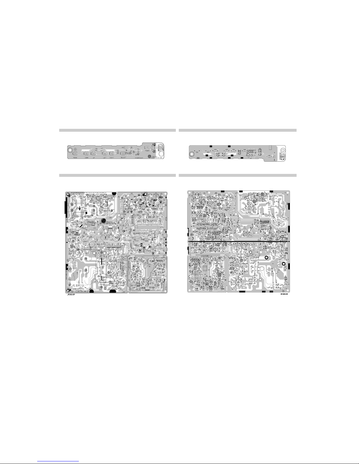
- 44 -
- 45 -
PRINTED CIRCUIT BOARD
3. MAIN BOARD (Component Side)
4. MAIN BOARD (Solder Side)
1. CONTROL BOARD (Component Side)
2. CONTROL BOARD (Solder Side)
Page 43

Jul. 2004
P/NO : 3828TSL105C Printed in China
 Loading...