

Page 1

COLOR MONIT OR
SER VICE MANUAL
Website:http://biz.LGservice.com
E-mail:http://www.LGEservice.com/techsup.html
CAUTION
BEFORE SERVICING THE UNIT,
READ THE SAFETY PRECAUTIONS IN THIS MANUAL.
MENU SELECT
Brightview
MODEL: T710PH
(T710PHJ-AL**E, AL**Q)
CHASSIS NO. : CA-128
( ) **Same model for SVC
*Same looking with new chassis.
Issue Date; 2003. 6.
Page 2
1. PICTURE TUBE
Size : 17 inch (Flat Square Tube)
DefIection Angle : 90°
Neck Diameter : 29.1mm
Diagonal Inch : 16.0”
Dot Pitch : 0.25mm
Face Treatment : Anti-Glare,
Anti-Static&Anti-Reflection
2. SIGNAL
2-1. Horizontal & Vertical Sync
1) Input Voltage Level: Low=0~1.2V, High=2.5~5.5V
2) Sync Polarity : Positive or Negative
3) Seperated Sync Signal
2-2. Video Input Signal
1) Voltage Level : 0 ~ 0.7 Vp-p
a) Color 0, 0 : 0 Vp-p
b) Color 7, 0 : 0.467 Vp-p
c) Color 15, 0 : 0.7 Vp-p
2) Input Impedance : 75 Ω
3) Video Color : R, G, B Analog
4) Signal Format : Refer to the Timing Chart
2-3. Signal Connector
15-pin Attached Connector
2-4. Scanning Frequency
Horizontal : 30 ~ 85kHz
Vertical : 50 ~ 160Hz
3. POWER SUPPLY
3-1. Power Range
AC 100-240V~ 50/60Hz, 2.0A Max.
3-2. Power Consumption
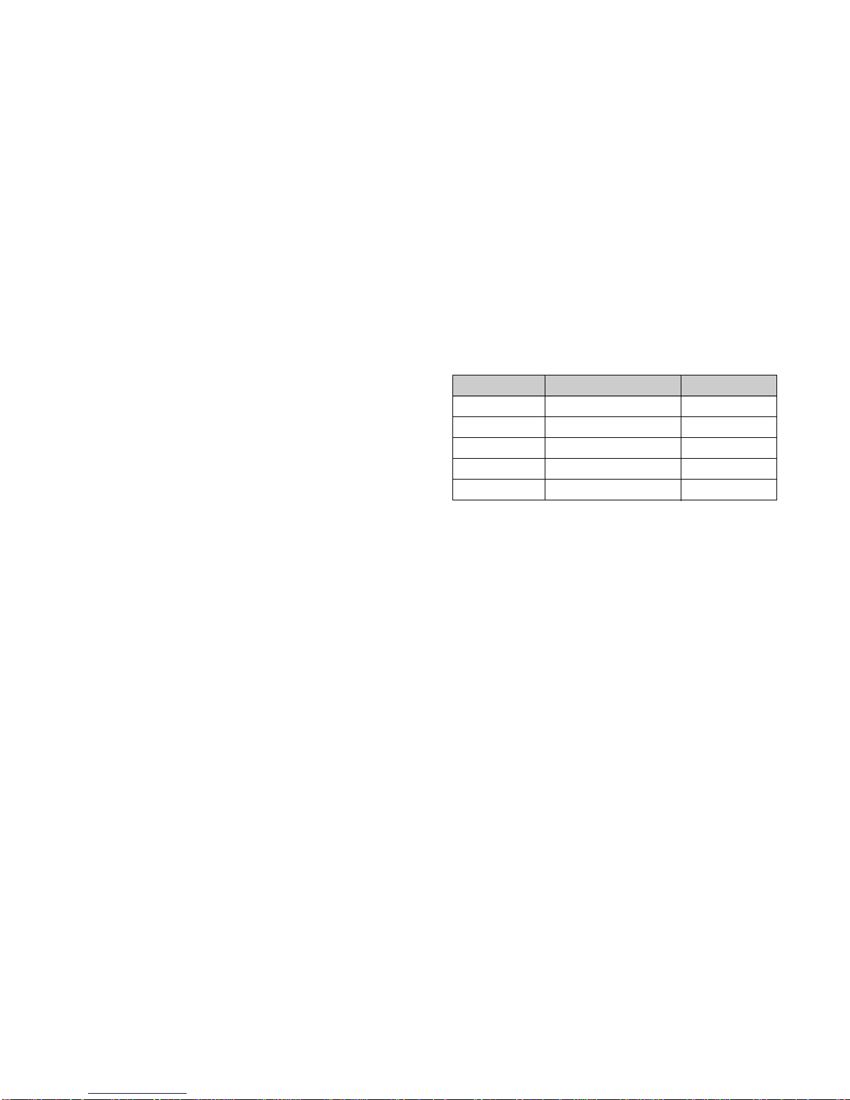
4. DISPLAY AREA
4-1. Active Video Area :
• Max Image Size - 325.1 x 243.8 mm (12.79" x 9.59")
• Preset Image Size - 315 x 230 mm (12.40" x 9.06")
4-2. Display Color : Full Colors
4-3. Display Resolution : 1280 x 1024 / 75Hz(Max)
(Non-Interlace)
4-4. MTBF : 50,000HRS
5. ENVIRONMENT
5-1. Operating Temperature: 0°C ~ 40°C (Ambient)
5-2. Relative Humidity : 10%~ 90%
(Non-condensing)
5-3. Altitude : 5,000m
6. DIMENSIONS (with TILT/SWIVEL)
Width : 400mm (15.75 inch)
Depth : 411mm (16.18 inch)
Height : 401mm (15.79 inch)
7. WEIGHT (with TILT/SWIVEL)
Net Weight : 15.7 kg (34.62 lbs.)
Gross Weight : 18.3 kg (40.35 lbs.)
CONTENTS
- 2 -
SPECIFICATIONS ................................................... 2
SAFETY PRECAUTIONS ........................................ 3
TIMING CHART ....................................................... 4
OPERATING INSTRUCTIONS ................................ 5
WIRING DIAGRAM ................................................. 6
BLOCK DIAGRAM ................................................... 8
ADJUSTMENT ....................................................... 11
TROUBLESHOOTING GUIDE .............................. 13
EXPLODED VIEW...................................................23
REPLACEMENT PARTS LIST ............................... 25
PIN CONFIGURATION........................................... 30
SCHEMATIC DIAGRAM......................................... 32
PRINTED CIRCUIT BOARD................................... 34
SPECIFICATIONS
MODE
MAX
NORMAL (ON)
STAND-BY
SUSPEND
DPMS OFF
POWER CONSUMPTION
90 W
73 W
less than 15 W
less than 15 W
less than 5 W
LED COLOR
GREEN
GREEN
AMBER
AMBER
AMBER
Page 3

SAFETY-RELATED COMPONENT WARNING!
There are special components used in this color monitor
which are important for safety. These parts are marked
on the schematic diagram and the replacement
parts list. It is essential that these critical parts should be
replaced with the manufacturer's specified parts to
prevent X-radiation, shock, fire, or other hazards. Do not
modify the original design without obtaining written
permission from manufacturer or you will void the original
parts and labor guarantee.
CAUTION:
No modification of any circuit should be
attempted.
Service work should be performed only after
you are thoroughly familiar with all of the
following safety checks and servicing
guidelines.
SAFETY CHECK
Care should be taken while servicing this color monitor
because of the high voltage used in the deflection circuits.
These voltages are exposed in such areas as the
associated flyback and yoke circuits.
FIRE & SHOCK HAZARD
An isolation transformer must be inserted between the
color monitor and AC power line before servicing the
chassis.
• In servicing, attention must be paid to the original lead
dress specially in the high voltage circuit. If a short
circuit is found, replace all parts which have been
overheated as a result of the short circuit.
• All the protective devices must be reinstalled per the
original design.
• Soldering must be inspected for the cold solder joints,
frayed leads, damaged insulation, solder splashes, or
the sharp points. Be sure to remove all foreign
materials.
IMPLOSION PROTECTION
All used display tubes are equipped with an integral
implosion protection system, but care should be taken to
avoid damage and scratching during installation. Use only
same type display tubes.
X-RADIATION
The only potential source of X-radiation is the picture tube.
However, when the high voltage circuitry is operating
properly there is no possibility of an X-radiation problem.
The basic precaution which must be exercised is keep the
high voltage at the factory recommended level; the normal
high voltage is about 25.8kV. The following steps describe
how to measure the high voltage and how to prevent Xradiation.
Note : It is important to use an accurate high voltage
meter calibrated periodically.
• To measure the high voltage, use a high impedance
high voltage meter, connect (–) to chassis and (+) to
the CDT anode cap.
• Set the brightness control to maximum point at full
white pattern.
• Measure the high voltage. The high voltage meter
should be indicated at the factory recommended level.
• If the meter indication exceeds the maximum level,
immediate service is required to prevent the possibility
of premature component failure.
• To prevent X-radiation possibility, it is essential to use
the specified picture tube.
CAUTION:
Please use only a plastic screwdriver to protect yourself
from shock hazard during service operation.
SAFETY PRECAUTIONS
- 3 -
Page 4
- 4 -
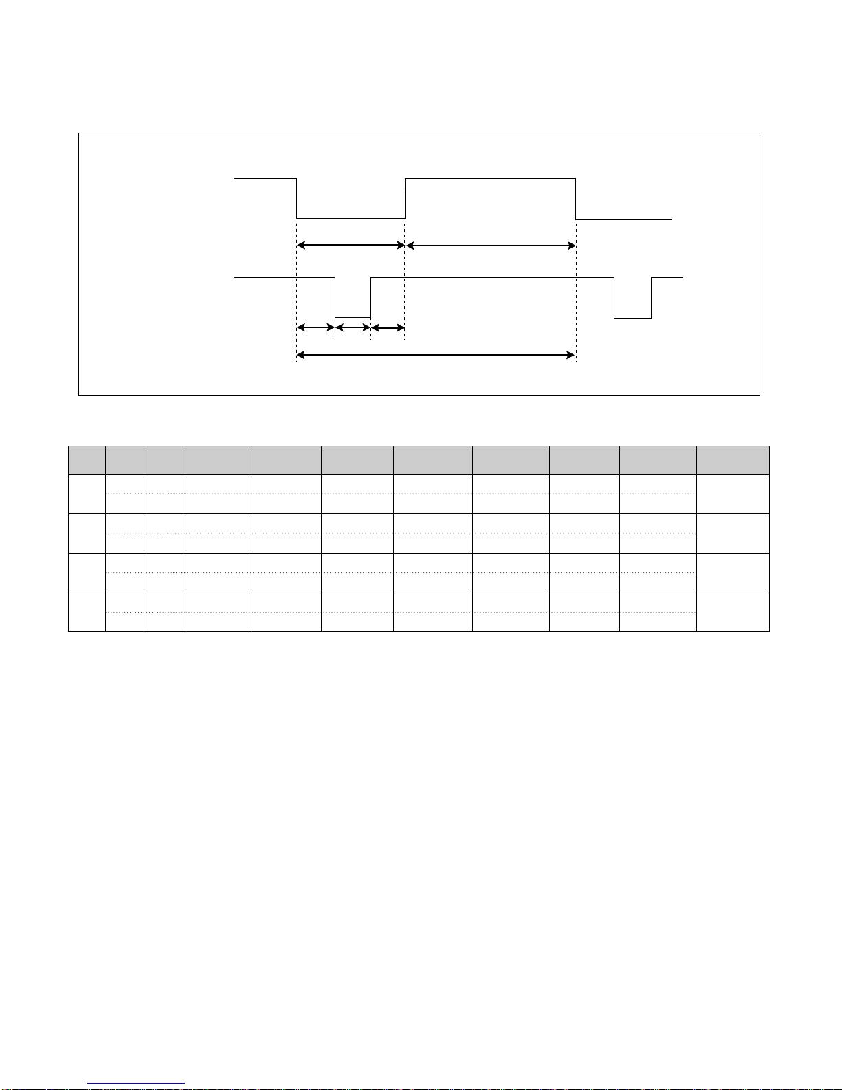
TIMING CHART
VIDEO
SYNC
C
E
D
F
A
B
<< Dot Clock (MHz), Horizontal Frequency (kHz), Vertical Frequency (Hz), Horizontal etc... (µs), Vertical etc... (ms) >>
* No Composite Mode.
H – 37.50 26.67 20.32 6.35 2.03 3.81 0.51
V – 74.99 13.335 12.802 0.533 0.080 0.427 0.026
Mode
H/V
Sort
1
2
3
4
640x480
75Hz
Sync
Polarity
Frequency
Total Period
(A)
Video Active
Time (B)
Sync Duration
(E)
Blanking Time
(C)
Back Porch
(F)
Front Porch
(D)
Resolution
H + 53.68 18.63 14.22 4.41 1.14 2.70 0.57
V + 85.07 11.755 11.178 0.577 0.056 0.503 0.018
H + 68.677 14.561 10.836 3.725 1.016 2.201 0.508
V + 85.00 11.764 11.182 0.582 0.044 0.524 0.014
1280x1024
75Hz
800x600
85Hz
1024x768
85Hz
H + 79.976 12.504 9.481 3.022 1.067 1.837 0.119
V + 75.025 13.329 12.804 0.525 0.038 0.475 0.013
Page 5
- 5 -
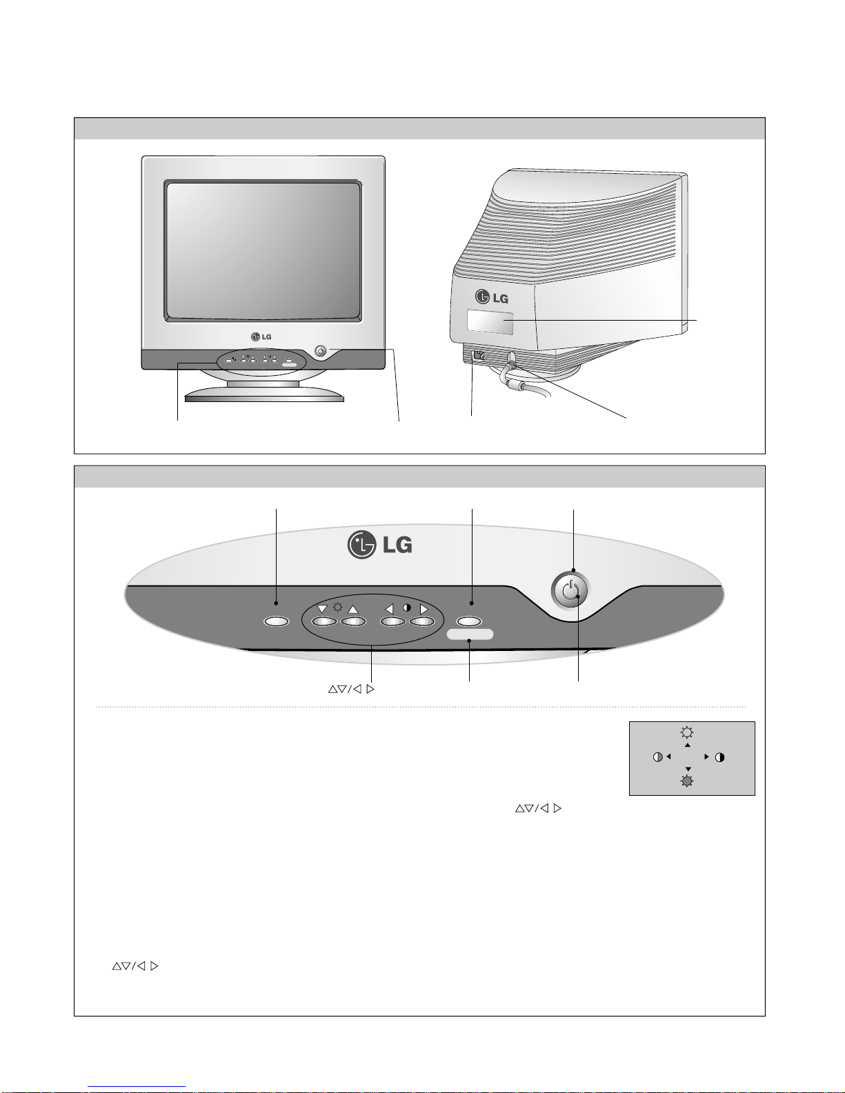
OPERATING INSTRUCTIONS
1. Power ON/OFF Button
Use
this button to turn the monitor ON or OFF.
2. Power Indicator
This indicator lights up green when the monitor operates
normally; in DPMS (Energy Saving) mode, - stand-by,
suspend, or power off mode - its color changes to
orange, and if abnormal or damaging circuit turns out
orange blink.
3. Select Button
Use this button to enter a selection in the on screen
display.
4. Button
Use these buttons to choose or adjust items in the on
screen display.
5. MENU Button
Use this button to enter or exit the on screen display.
6. Brightview Button(To apply the High brightness)
Use this button to select brightview function.
(TEXT/PHOTO/MOVIE/NORMAL)
FRONT VIEW REAR VIEW
AC Power Socket
Signal Connector
ID Label
Front Control Panel
MENU SELECT
Brightview
Power ON/OFF Button
See Front Control Panel
MENU SELECT
Brightview
Buttons
MENU Button
Power Button
Power (DPMS) Indicator
SELECT Button
Brightiew Button
<Shortcut Keys>
• Brightness and Contrast can be
adjusted directly without entering
the On Screen Display (OSD)
system.
Press the buttons to adjust the settings and then
the MENU button to save all changes. The Brightness and
Contrast functions are also available in the On Screen
Display (OSD) menu.
100
100
Page 6
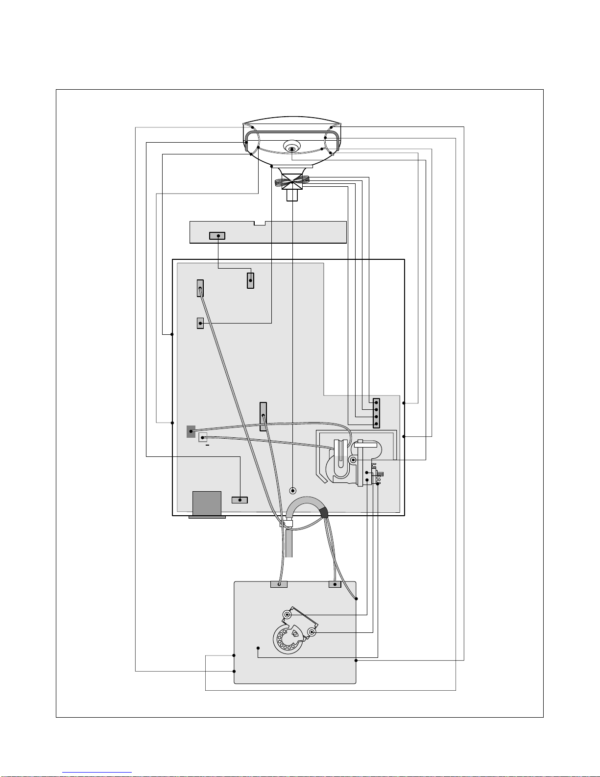
WIRING DIAGRAM
- 6 -
P501
P201
P405
P301
P302
G2
P702
P701
T1
P402
P902
S
+
S
Signal
Cable
AC
Socket
FBT
Page 7
- 7 -
DISASSEMBLY
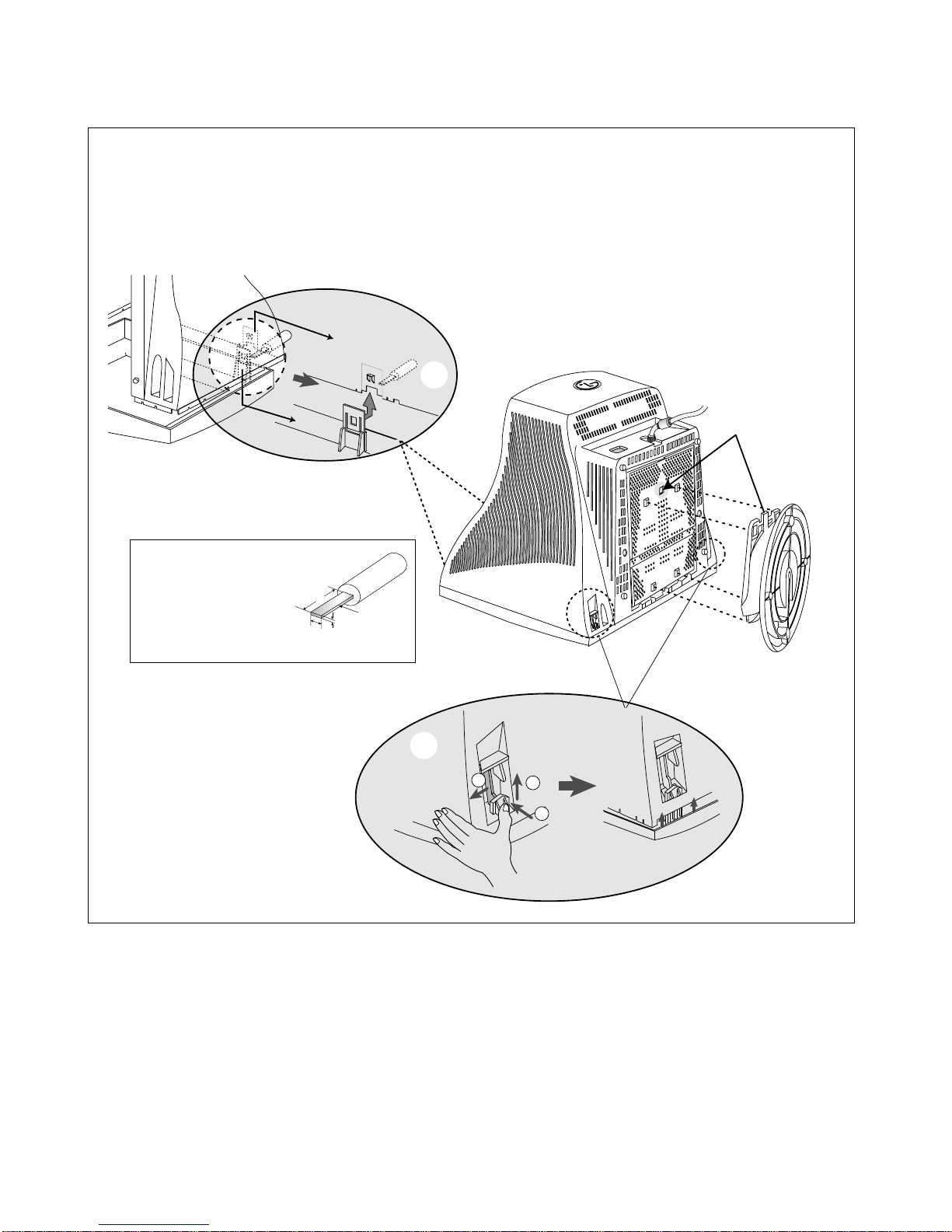
1. TILT/SWIVEL & BACK COVER REMOVAL
1) Set the monitor face downward.
2) Carefully remove the Tilt/Swivel by pulling it upward.
3) Pressing the latch (b), Back cover by pushing it upward.
4) Release the latch (c). (See Tip Spec.)
5) Slide the Back Cover away from the Front Cabinet of the monitor.
Tip Spec.
A(Width) : 5.0~15.0mm
B(Depth) : 0.6~0.9mm
C(Height) : 12.0mm
Back Cover
(c)
Cabinet
(a)
C
Tip
B
A
(b)
1
3
2
Page 8
BLOCK DIAGRAM
- 8 -
Input_power
100~240VAC
(50/60Hz)
Line
Filter
Degaussing
Circuit
[ OSD Control ]
Power
Control
(IC901)
TILT
Control
Circuit
6.3V
15V
E
2
PROM
(IC402)
5V
H-sync Signal
V-sync Signal
I
2
C DATA(SDA)
I
2
C CLOCK(SCL)
VIDEO
OSD+pre_Amp
(IC302)
Signal
cable
RGB
VIDEO
Main_Amp
(IC303)
H/V Sync Processor
( IC701 )
TDA4841
V-out
( IC601)
TDA4867J
H-out
(Q706)
H-Linearity
Correction
Circuit
X-RAY
Protection
Circuit
Dynamic
FOCUS
Circuit
Vertical Blanking,
- 160V
15V
D/D
Feed Back
12V
MICOM
(IC401)
SCL / SDA
H/V sync
PWM control signal
15V
15V
50V
DY CDT
Heater ( 6.3V )
I
2
C
I
2
C
I
2
C
H/V
Sync
Screen
H.V
R/G/B
Bias
R/G/B
Contrast
H-Drive
B-Drive
B+
15V
BRIGHTNESS/CONTRAST
COLOR CURVE
H / V POSITION
H / V SIZE
SPCC
TRAPEZOID
PIN BALANCE
PARALLELOGRAM
TOP CORNER
BOTTOM CORNER
RECALL
DEGAUSSING
MOIRE
LANGUAGE
RESET
OSD TIME
TILT
VIDEO INPUT LEVEL
BRIGHT VIEW
TEXT
PHOTO
MOVIE
MORMAL
DPM Control
Circuit
400V
15V
6.3V
15V 80V
Voltage
feedback
Voltage
feedback
Degaussing
Coil
Dynamic Focus
Static Focus
TILT
Coil
50V
80V
15V
G2
G1
DC/DC Converter
FBT
( T701 )
Regulation
Circuit
SMPS
(T901)
5V 15V
CUT-OFF IC
(IC304)
5V
Auto
Beam
Limit
Page 9

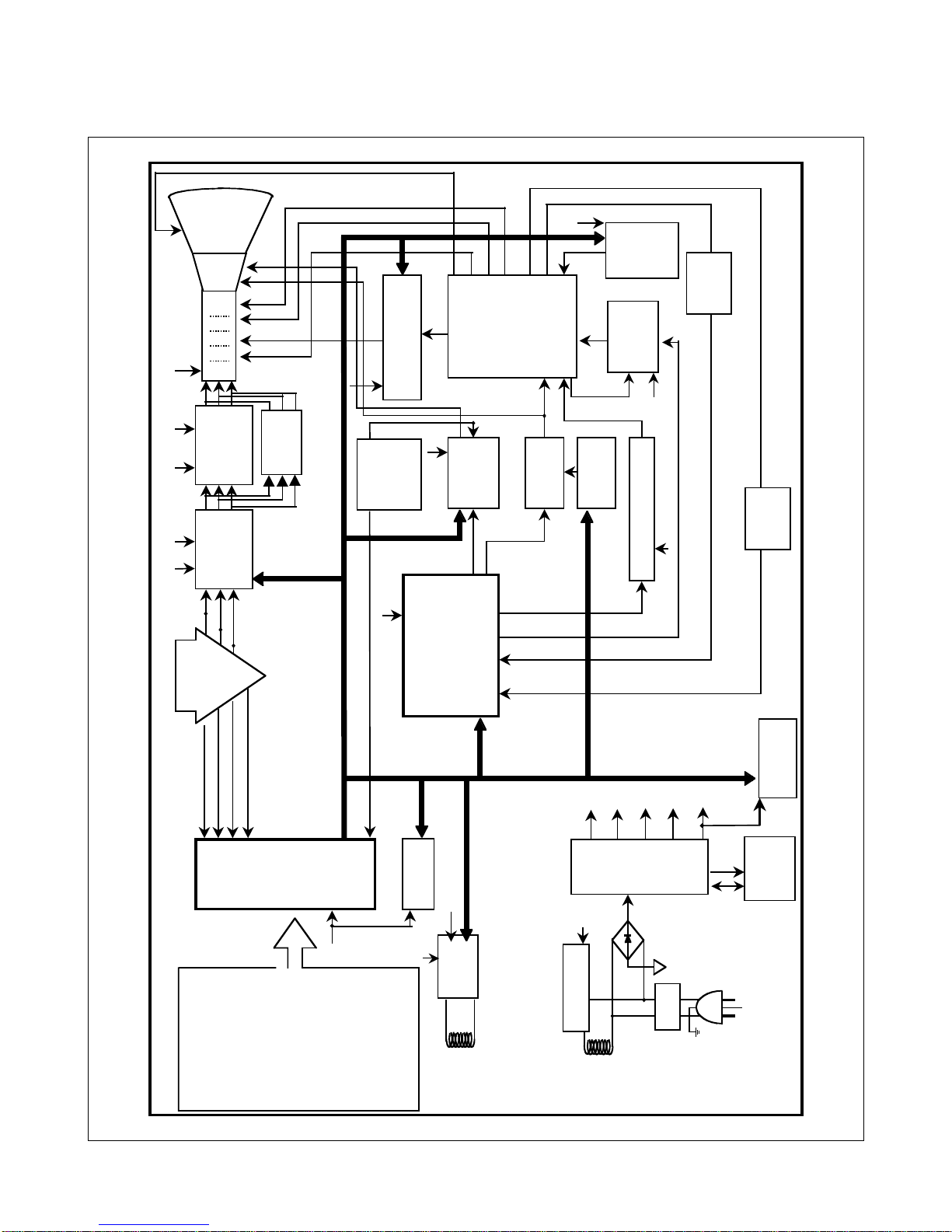
DESCRIPTION OF BLOCK DIAGRAM
- 9 -
1. Line Filter & Associated Circuit.
This is used for suppressing noise of power input line
flowing into the monitor and/or some noise generated in
this monitor flowing out through the power input line.
That is to say, this circuit prevents interference between
the monitor and other electric appliances.
2. Degauss Circuit & Coil.
The degauss circuit consists of the degaussing coil, the
PTC(Positive Temperature Coefficient) thermistor(TH901),
and the relay(RL901). This circuit eliminates abnormal
color of the screen automatically by degaussing the
shadow mask in the CRT during turning on the power
switch. When you need to degauss in using the monitor,
select DEGAUSS on the OSD menu.
3. SMPS(Switching Mode Power Supply).
This circuit is working of 90~264V AC(50/60Hz).
The operation procedure is as follows:
1) AC input voltage is rectified and smoothed by the bridge
diodes (D900) and the capacitor (C908).
2) The rectified voltage(DC) is applied to the primary coil
of the transformer(T901).
3) The control IC(IC901) generates switching pulse to turn
on and off the primary coil of the transformer (T901)
repeatedly.
4) Depending on turn ratio of the transformer, the
secondary voltages appear at the secondary coils of the
transformer(T901).
5) These secondary voltages are rectified by each
diode(D941, D942, D951, D961, D962, D971) and operate
other circuit. (horizontal and vertical deflection, video
amplifier, ...etc.)
4. X-ray Protection.
If the high voltage of the FBT reaches up to 29kV (abnormal
state), IC401(MICOM) pin 35 Sensing from FBT directly.
Then MICOM control IC701 (Deflection controller) to stop
Horizontal drive pulse and stop Horizontal Deflection.
5. Micom(Microprocessor) Circuit.
The operating procedure of Micom(Microprocessor) and
its associated circuit is as follows:
1) H and V sync signal is supplied from the signal cable.
2) The Micom(IC401) distinguishes polarity and
frequency of H and V sync.
3) The Micom sets operating mode and offers the
controlled data. (H-size, H-position, V-size, ... etc.)
4) The controlled data of each mode is stored in itself.
5) User can adjust screen condition by each OSD
function. The data of the adjusted condition is stored
in EEPROM(IC402).
6. Horizontal and Vertical Oscillation.
This circuit generates the horizontal pulse and the vertical
pulse by taking the H and V sync signal.
This circuit consists of the TDA4867J(IC601) and the
associated circuit.
7. D/D(DC to DC) Converter.
This circuit supplies DC voltage to the horizontal deflection
output circuit by increasing DC 50V which is the
secondary voltage of the SMPS in accordance with the
input horizontal sync signal.
8. Side-Pincushion & Trapezoid Correction Cirucit.
This circuit improves the side-pincushion and the
trapezoid distortion of the screen by mixing parabola and
saw-tooth wave to output of the horizontal deflection D/D
converter which is used for the supply voltage(B + ) of the
deflection circuit.
9. Horizontal Deflection Output Circuit.
This circuit makes the horizontal deflection by supplying
the saw-tooth current to the horizontal deflection yoke.
10. High Voltage Output & FBT(Flyback Transformer).
The high voltage output circuit is used for generating pulse
to the primary coil of the FBT(Flyback Transformer)
secondary of the FBT and it is supplied to the anode,
focus, and screen voltage of the CRT.
11. H-Linearity Correction Circuit.
This circuit corrects the horizontal linearity for each
horizontal sync frequency.
12. Vertical Output Circuit.
This circuit takes the vertical ramp wave from the
TDA4841(IC701) and performs the vertical deflection by
supplying the saw-tooth current to the vertical deflection
yoke.
13. Dynamic Focus Output Circuit.
This circuit takes the horizontal and the vertical parabola
waves from the TDA4841(IC701) and amplifies it to
maintain constant focus on center and corners in the
screen.
14. H& V Blanking and Brightness Control.
Blanking circuit eliminates retrace line by supplying
negative pulse to the G1 of the CRT. And Brightness
control uses the R/G/B cut-off DC level by IIC line.
Page 10

- 10 -
15. Image Rotation (Tilt) Circuit.
This circuit corrects the tilt of the screen by supplying the
image rotation signal to the tilt coil which is attached near
the deflection yoke of the CRT.
16. Video Pre-Amp Circuit.
This circuit amplifies the analog video signal from 0-0.7V
to 0-4V. It is operated by taking the clamp, R, G, B drive
and contrast signal from the Micom(IC401).
17. Video Output Amp Circuit.
This circuit amplifies the video signal which comes from
the video pre-amp circuit and amplified it to applied the
CRT cathode.
Page 11

ADJUSTMENT
- 11 -
GENERAL INFORMATION
All adjustment are thoroughly checked and corrected
when the monitor leaves the factory, but sometimes
several adjustments may be required.
Adjustment should be following procedure and after
warming up for a minimum of 30 minutes.
• Alignment appliances and tools.
- IBM compatible PC.
- Programmable Signal Generator.
(eg. VG-819 made by Astrodesign Co.)
- EPROM or EEPROM with saved each mode data.
- Alignment Adaptor and Software.
- Digital Voltmeter.
- White Balance Meter.
- Luminance Meter.
- High-voltage Meter.
AUTOMATIC AND MANUAL DEGAUSSING
The degaussing coil is mounted around the CDT so that
automatic degaussing when turn on the monitor. But a
monitor is moved or faced in a different direction, become
poor color purity cause of CDT magnetized, then
press
DEGAUSS on the OSD menu.
ADJUSTMENT PROCEDURE & METHOD
-Install the cable for adjustment such as Figure 1and run
the alignment program on the DOS for IBM compatible PC.
-Set external Brightness and Contrast volume to max position.
1. Checked for B+ Voltage.
1) Display cross hatch pattern at Mode 4.
2) Check D961 voltage to 50.0V ± 1V with.
2. Adjustment for High-Voltage.
1) Display cross hatch pattern at Mode 4.
2) DIST.ADJ→CTRL PWM → High Voltage Command.
3) Adjust High Voltage to 25.8kV
±
0.1 kVdc.
4) Press Enter Key.
3. Adjustment for Factory Mode (Preset Mode).
1) Display cross hatch pattern at Mode 1.
2) Run alignment program for T710PHJ on the IBM
compatible PC.
3) EEPROM → ALL CLEAR → Y(Yes) command.
<Caution> Do not run this procedure unless the
EEPROM is changed. All data in EEPROM (mode
data and color data) will be erased.
4) Power button of the monitor turn off →turn on.
5) COMMAND→PRESET START→Y(Yes) command.
6) DIST. ADJ. → CTRL PWM → TILT command.
7) Adjust tilt as arrow keys to be the best condition.
8) DIST. ADJ. → BALANCE command.
9) Adjust parallelogram as arrow keys to be the best
condition.
10)
Adjust balance of pin-balance as arrow keys to be
the best condition.
11)
DIST. ADJ. → FOS. ADJ command.
12)
Adjust V-SIZE as arrow keys to 230±2mm.
13)
Adjust V-POSITION as arrow keys to center of the
screen.
14)
Adjust H-SIZE as arrow keys to 310±2mm.
15)
Adjust H-POSITION as arrow keys to center of the
screen.
16)
Adjust S-PCC (Side-Pincushion) as arrow keys to be
the best condition.
17)
Adjust TRAPEZOID as arrow keys to be the best
condition.
18)
Save of the Mode 1~4.
19)
Display from Mode 2 to 4 and repeat above from
number 12) to 19)
20)
PRESET EXIT → Y (Yes) command.
4. Adjustment for White Balance and Luminance.
1) Set the White Balance Meter.
2) Press the DEGAUSS on the OSD menu for
demagnetization of the CDT.
3) COLOR ADJ. → LUMINANCE command of the
alignment program.
4) Set Brightness and Contrast to Max position.
5) Display color 0,0 pattern at Mode 4.
6) COLOR ADJ.→ BIAS ADJ.→ COLOR No. → 1
command of the alignment program.
7) Check whether green color or not at R-BIAS and GBIAS to min position and B-BIAS to 127(7F) position
and Sub-Brightness to 205(CD) position. Adjust G2
(screen) command to 0.2
±
0.05FL of the raster
luminance.
8) Adjust R-BIAS and G-BIAS command to x=0.283
±
0.005 and y=0.298±0.005 on the White Balance
Meter with PC arrow keys.
9)
Adjust SUB-Brightnesscommand to 0.4±0.1FL of the
raster luminance.
10)
Adjust repeat number 8).
11)
push the “ENTER” key.
11-1)
COMMAND → PRESET START → Y(Yes) command.
12)
Display color 15,0 full white pattern at Mode 4.
13)
DRIVE ADJ.→ No 1. command.
Page 12

- 12 -
14)
Set Brightness and Contrast to Max position.
15)
Set SUB-CONTRAST 127(7F) (decimal) position.
16)
Set B-DRIVE to 85(55) at DRIVE of the alignment
program.
17-1)
Adjust R-DRIVE and G-DRIVE command to white
balance x=0.283
±
0.003 and y=0.298±0.003 on the
White Balance Meter with PC arrow keys.
17-2)
Display color 15,0 window pattern (70x70mm) at mode 4.
18)
Adjust SUB-CONTRAST command to 50±2FL .
19)
push the “ENTER” key.
20)
Display color 15,0 full white patten at Mode 4..
21)
COLOR ADJ. → LUMINANCE → ABL command.
22)
Adjust ABL to 32±1FL of the luminance.
23)
push the “ENTER” key, and “COMMAND →
PRESET EXIT → Y(Yes)” command.
24)
Exit from the program.
5. Input EDID Data.
1) Display color 15,0 cross hatch pattern at Mode 4.
2) EEPROM → Write EDID command and confirm
“EDID Write OK!!” message of monitor.
3) Exit from the alignment program.
4) Power switch OFF/ON for EDID data save.
6. Adjustment for Focus.
1) Set the Brightness and Contrast to max position.
2) Display H character in full screen at Mode 4.
3) Adjust two Focus control on the FBT that focus
should be the best condition.
Page 13
- 13 -
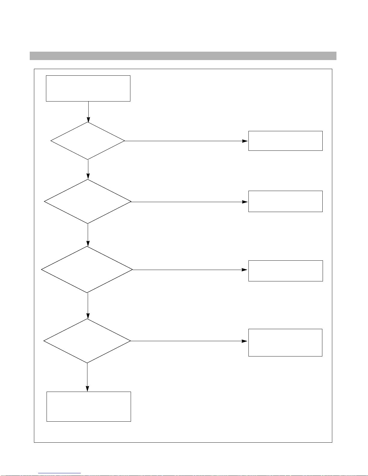
1. NO POWER
NO POWER
(POWER INDICATOR OFF)
TROUBLE IN
D900
TROUBLE IN FUSE
(F901)
TROUBLE IN
IC901
TROUBLE IN
D941, D942, D951,
D961, D962, D971
TROUBLE IN
Q903, Q952,
Q951, Q942, Q941
CHECK
FUSE OK?
CHECK
C908 VOLTAGE?
(AC120V: 160VDC,
AC220V: 304VDC)
NO
YES
YES
YES
YES
NO
NO
NO
CHECK
IC901 PIN 6
WAVEFORM
?
CHECK
D941, D942,
D951, D961, D962, D971
VOLTAGE?
TROUBLESHOOTING GUIDE
Page 14
- 14 -
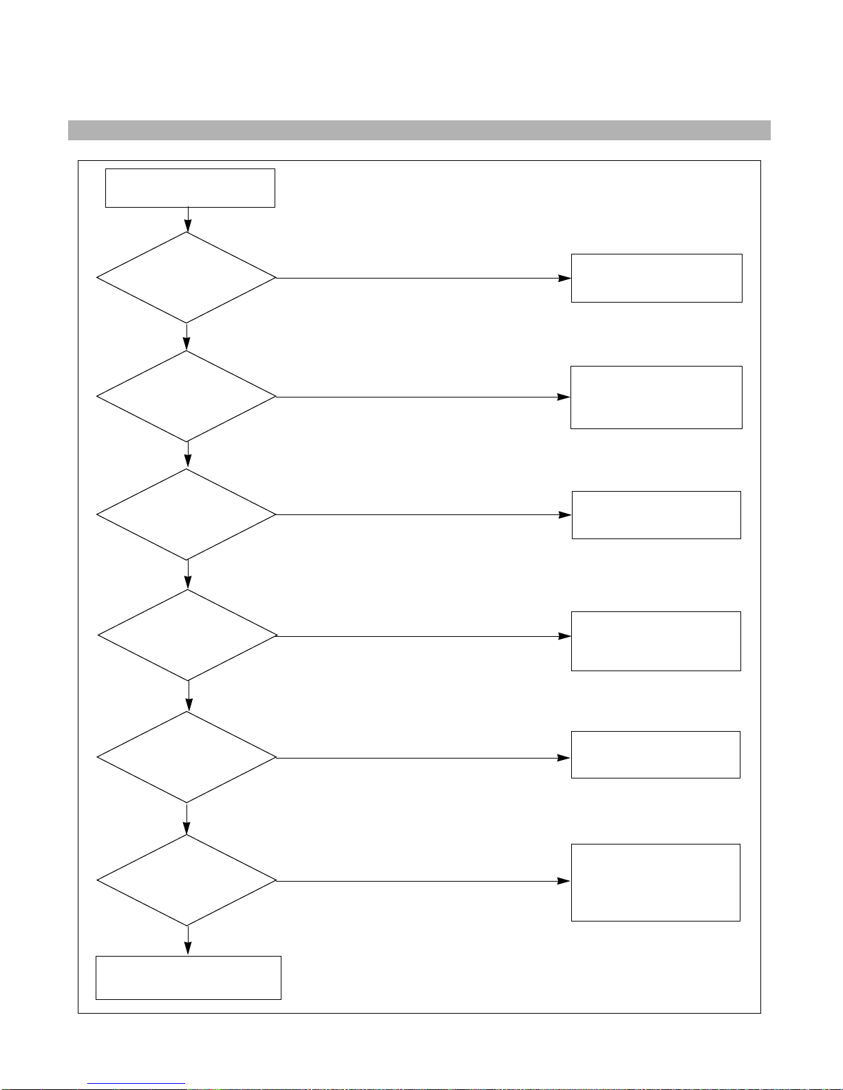
2. NO CHARACTER
NO CHARACTER
CHECK
IC302
PIN 18(5V) ?
CHECK
IC302 PIN 5, 6, 7?
CHECK
IC302 PIN 19, 20, 21 ?
CHECK
IC303
PIN 1, 2, 3 ?
CHECK
IC303 PIN 4 (80V)
PIN 8 (15V) ?
TROUBLE IN
P302 5V LINE
TROUBLE IN
PC SIGNAL,
P301 SIGNAL CABLE
TROUBLE IN
IC302
TROUBLE IN
P303 15V LINE/
80V LINE
TROUBLE IN IC303
NO
YES
NO
NO
YES
YES
YES
YES
NO
NO
CHECK
R, G, B CATHODE
VOLTAGE?
TROUBLE IN
R331~R333,
L311~L313,
D307~D312, IC304
TROUBLE IN
CRT SOCKET
YES
NO
Page 15
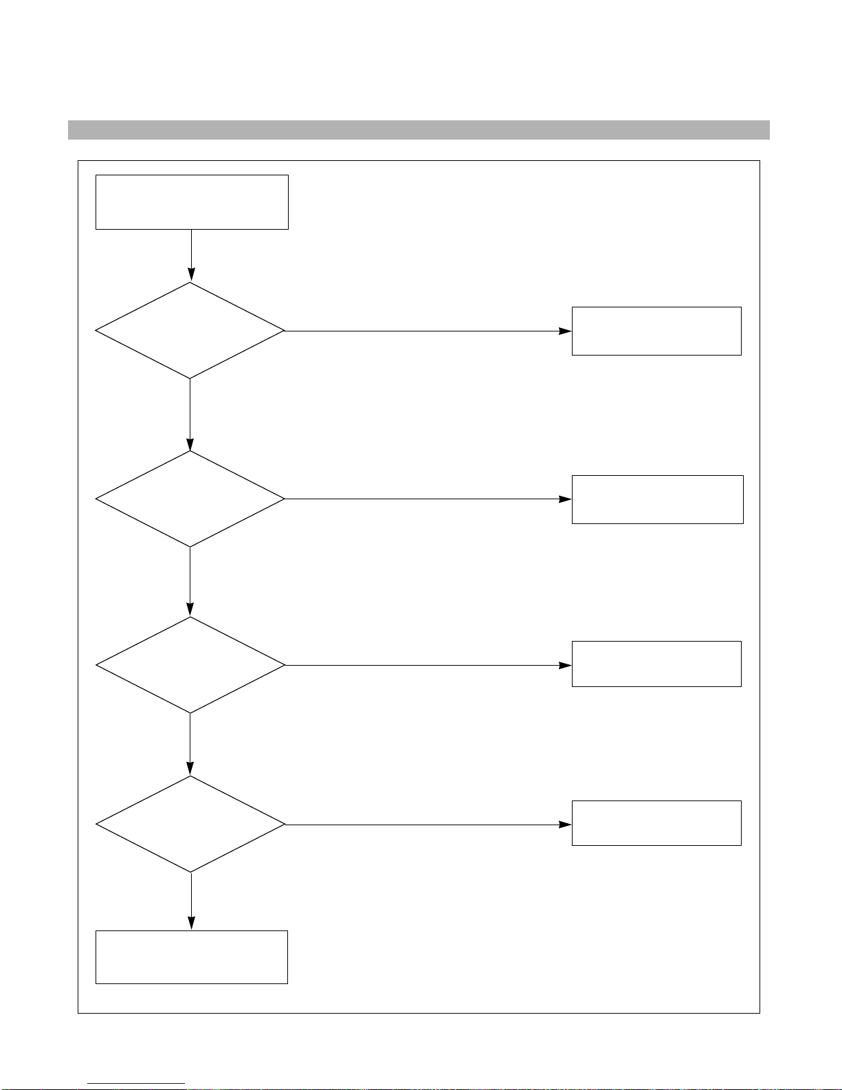
- 15 -
3. NO RASTER
NO VIDEO
(POWER INDICATOR ON)
CHECK
POWER INDICATOR
GREEN or AMBER?
CHECK
D712 ANODE
(-160V)?
CHECK
G1VOLTAGE?
(-55V~-15V)
TROUBLE IN
D712
TROUBLE IN
Q799
DPM MODE
(NO H and/or V SYNC)
AMBER
NO
GREEN
YES
NO
CHECK
CDT HEAT
VOLTAGE? (6.3V)
TROUBLE IN
D941, Q942, Q941
YES
NO
TROUBLE IN
CDT
YES
Page 16
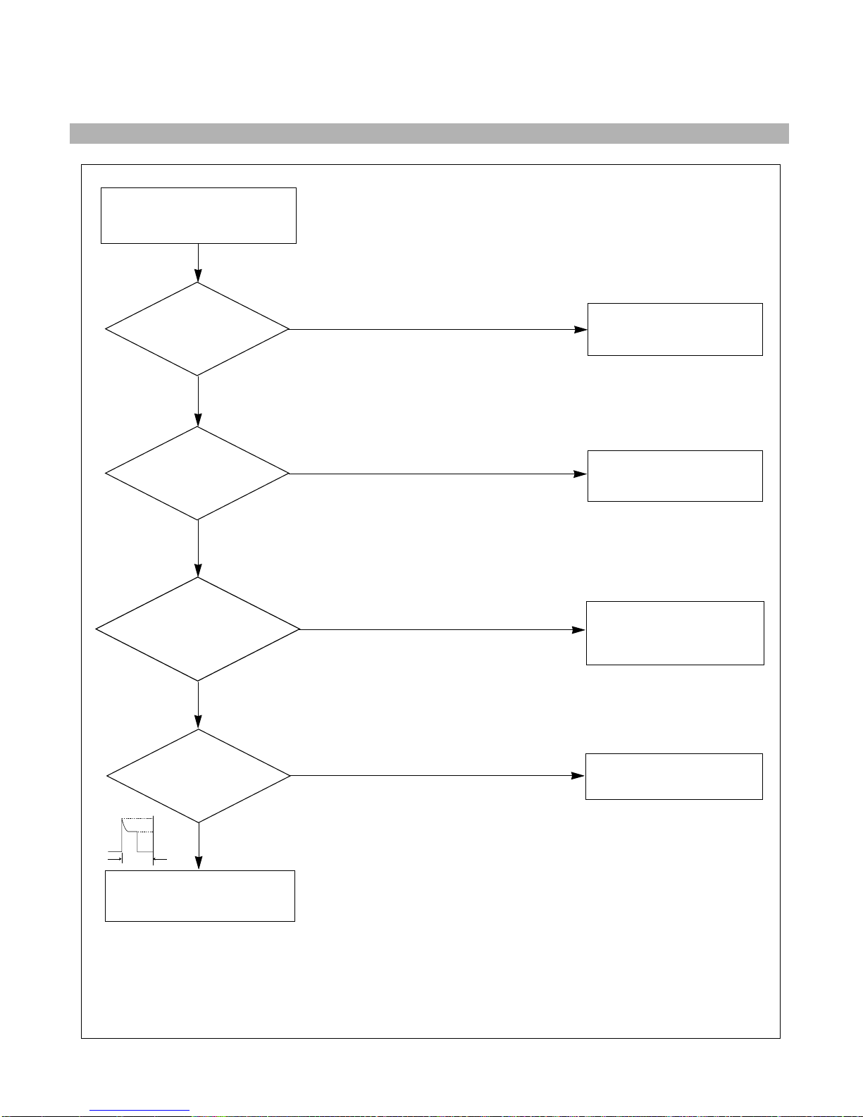
- 16 -
4. NO HORIZONTAL DEFLECTION
NO H-DEFLECTION
(ONE VERTICAL LINE)
CHECK
Q706?
CHECK
B+ VOLTAGE
(50V)?
CHECK
T701(FBT) PIN 2
(31KHZ 60V,
69KHZ 140V) ?
CHECK
Q705 COLLECTOR
WAVEFORM?
TROUBLE IN
Q706
TROUBLE IN
50V LINE
TROUBLE IN
Q719, Q720, D710
TROUBLE IN
Q705
TROUBLE IN
T701, P701
NO
NO
YES
YES
YES
YES
NO
NO
0V
T
Page 17
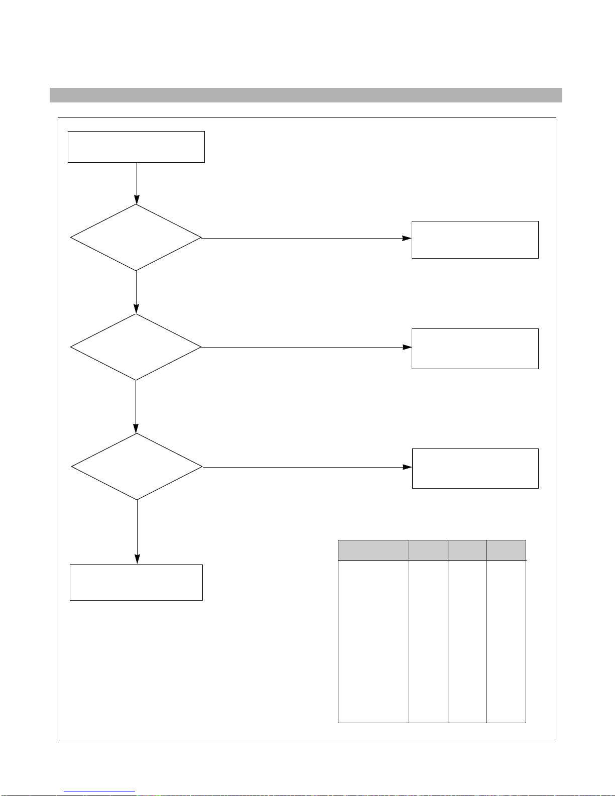
- 17 -
5. TROUBLE IN H-LINEARITY
UNBALANCED OF H-LIN.
CHECK
IC401
PIN 6, 7, 8 ?
CHECK
Q711~Q716?
CHECK
L703?
TROUBLE IN
IC401 (MICOM)
TROUBLE IN
Q711 ~ Q716
TROUBLE IN
L703
TROUBLE IN
C722, C723, C726, C729
NO
NO
NO
YES
YES
YES
Cs SIGNAL TABLE
HORIZONTAL
FREQUENCY(fH)
30K ~ 33.9K
34K ~ 38.9K
39K ~ 43.9K
44K ~ 48.9K
49K ~ 51.9K
52K ~ 57.9K
58K ~ 61.9K
62K ~ 65.9K
66K ~ 71K
74K ~ 77.9K
78.0K ~ 83.9K
84.0K ~ 86.9K
Cs1
L
L
L
L
H
L
L
L
H
H
H
H
Cs3
L
L
H
H
H
H
H
H
H
H
H
H
Cs2
L
H
L
L
L
H
H
H
H
H
H
H
Page 18
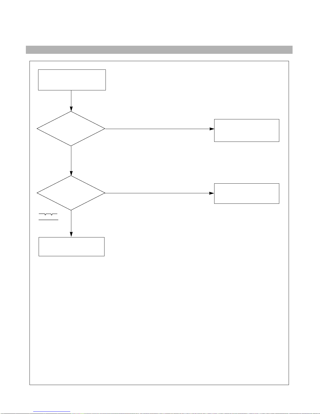
- 18 -
6. NO VERTICAL DEFLECTION
NO V-DEFLECTION
(ONE HORIZONTAL LINE)
CHECK
IC601 PIN 3
(15V+)?
CHECK
IC701 PIN 12, 13?
TROUBLE IN
R603 15V LINE
TROUBLE IN
IC701
TROUBLE IN
IC601, V-CIRCUIT
NO
YES
YES
NO
5V 12Pin
13Pin
Page 19
- 19 -
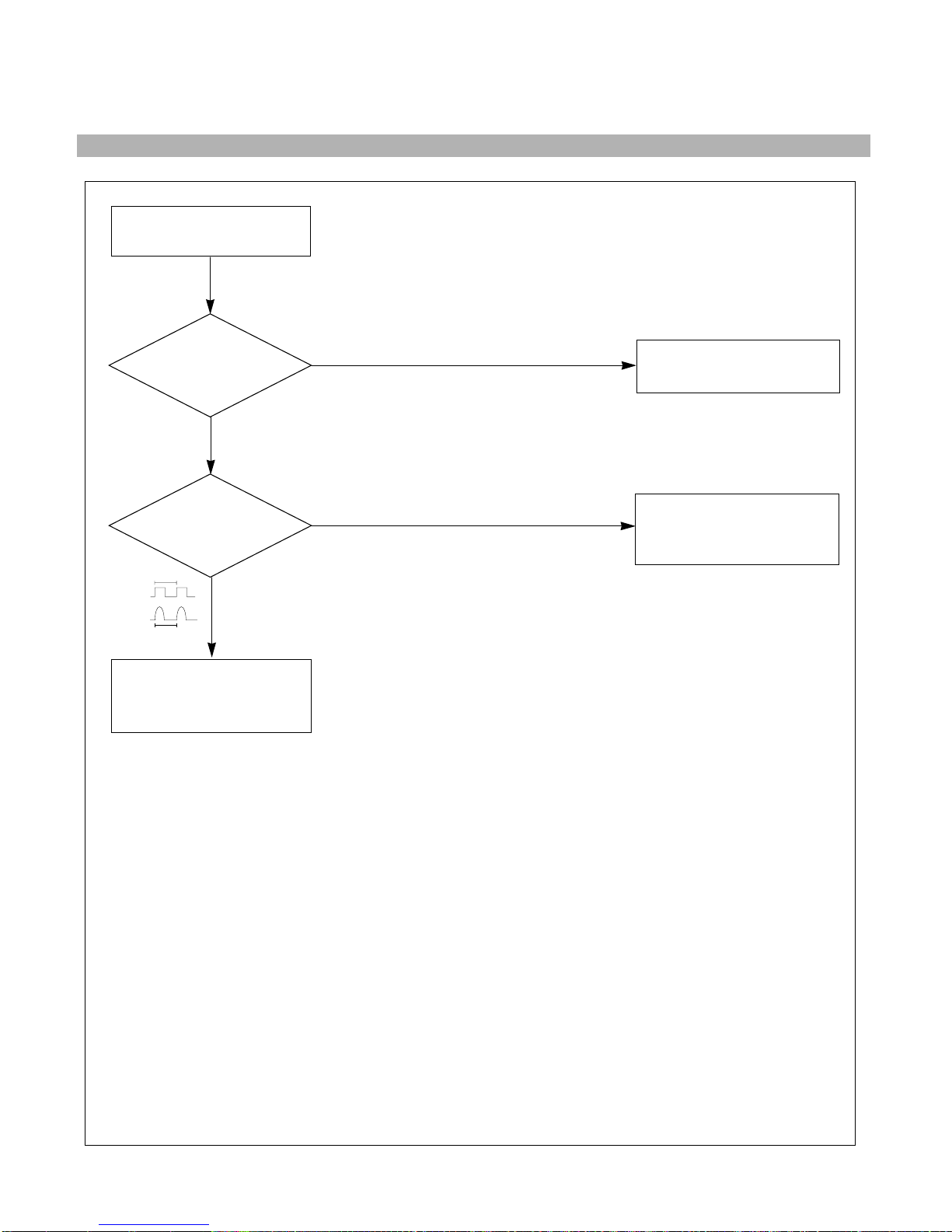
7. TROUBLE IN OSD
TROUBLE IN
OSD PERIPHERAL
CIRCUIT
NO OSD
TROUBLE IN
5V LINE
TROUBLE IN
IC401 PIN 29 (V-FBP),
IC701 PIN 1 LINE (H-FBP)
NO
YES
DC 5V
YES
NO
Pin 24
5V
Pin 1
FV
FH
CHECK
IC302 B
+
(5V)
?
(ENTER BUTTON MUST BE PRESSED.)
CHECK
IC302 PIN 1, 24
WAVEFORM?
Page 20
- 20 -
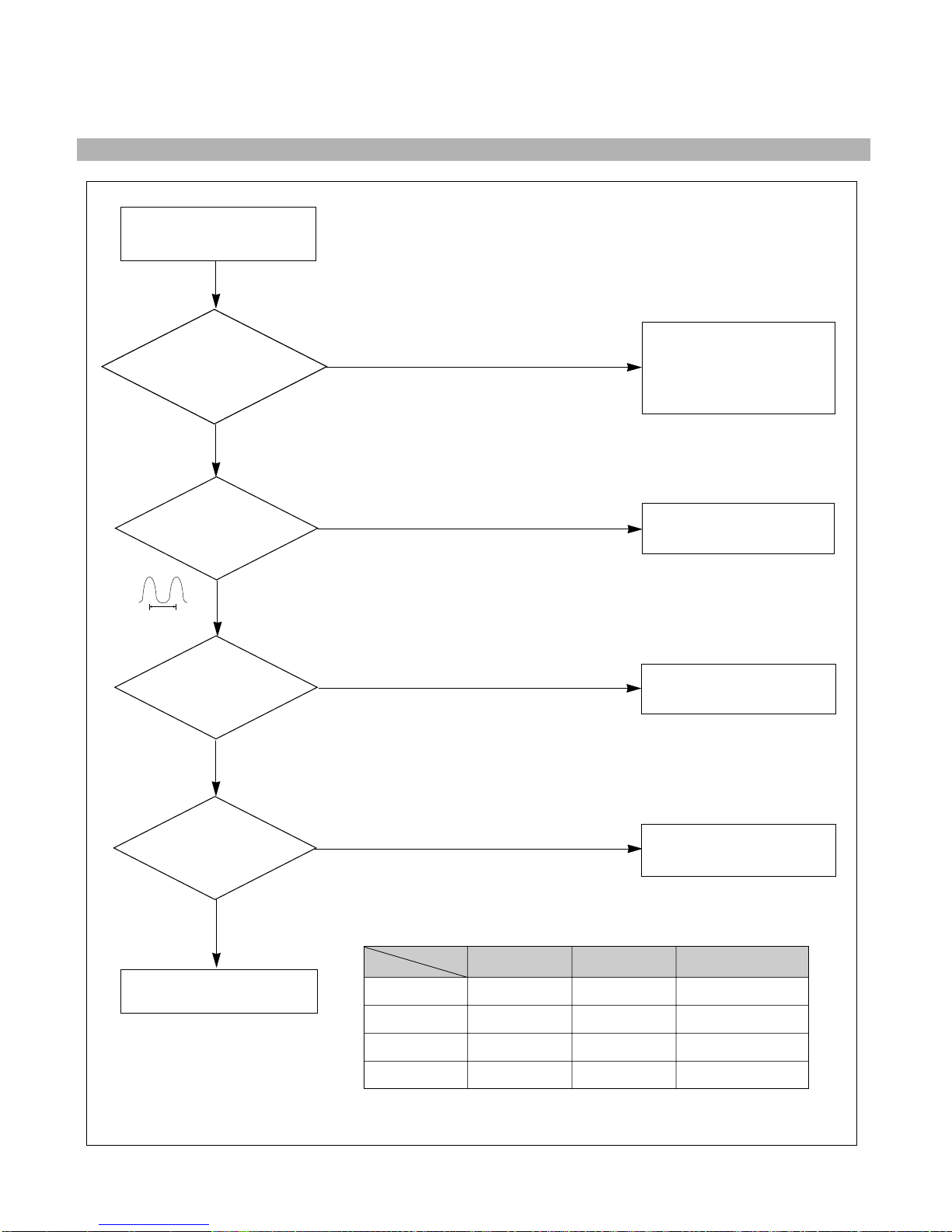
8. TROUBLE IN DPM
CHECK
IC401 (MICOM)
PIN 30, 31 (H/V INPUT)
SIGNAL?
CHECK
IC401 PIN 13
WAVEFORM?
CHECK
IC401 (MICOM)
PIN 2, 3 ?
CHECK
B+LINE
(6.3V,15V+) ?
CHECK PC,
(PC IS NOT GOING INTO
DPM OFF MODE)
TROUBLE IN
X401
TROUBLE IN
IC401 (MICOM)
TROUBLE IN
Q941, Q942, Q951, Q952,
TROUBLE IN PC
OFF MODE FAILURE
INPUT H/V SYNC SIGNAL
H/V SYNC
(NO OFF MODE.)
NO
NO
NO
NO (DPMF: 0V)
DPM TABLE
Mode
Item
NORMAL
STAND-BY
SUSPEND
OFF
DPM
H
L
L
L
LED
GREEN
AMBER
AMBER
AMBER
DPMS
H
H
H
L
YES
YES
SEE DPM TABLE
YES
YES
5V
12MHz
Page 21
- 21 -
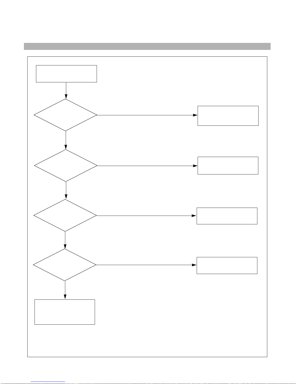
9. NO DEGAUSSING
CHECK
IC401 PIN 5
(0V)?
CHECK
Q953 COLLECTOR
VOLTAGE?
CHECK
P902 ?
CHECK
RL901?
TROUBLE IN
IC401 (MICOM)
TROUBLE IN
Q953
TROUBLE IN
P902
TROUBLE IN
RL901
TROUBLE IN
TH901,
DEGAUSSING COIL
NO DEGAUSSING
DC 15V
NO
NO
NO
NO
YES
YES
YES
YES
(DEGAUSS ON THE OSD MENU MUST BE PRESSED.)
Page 22
- 22 -
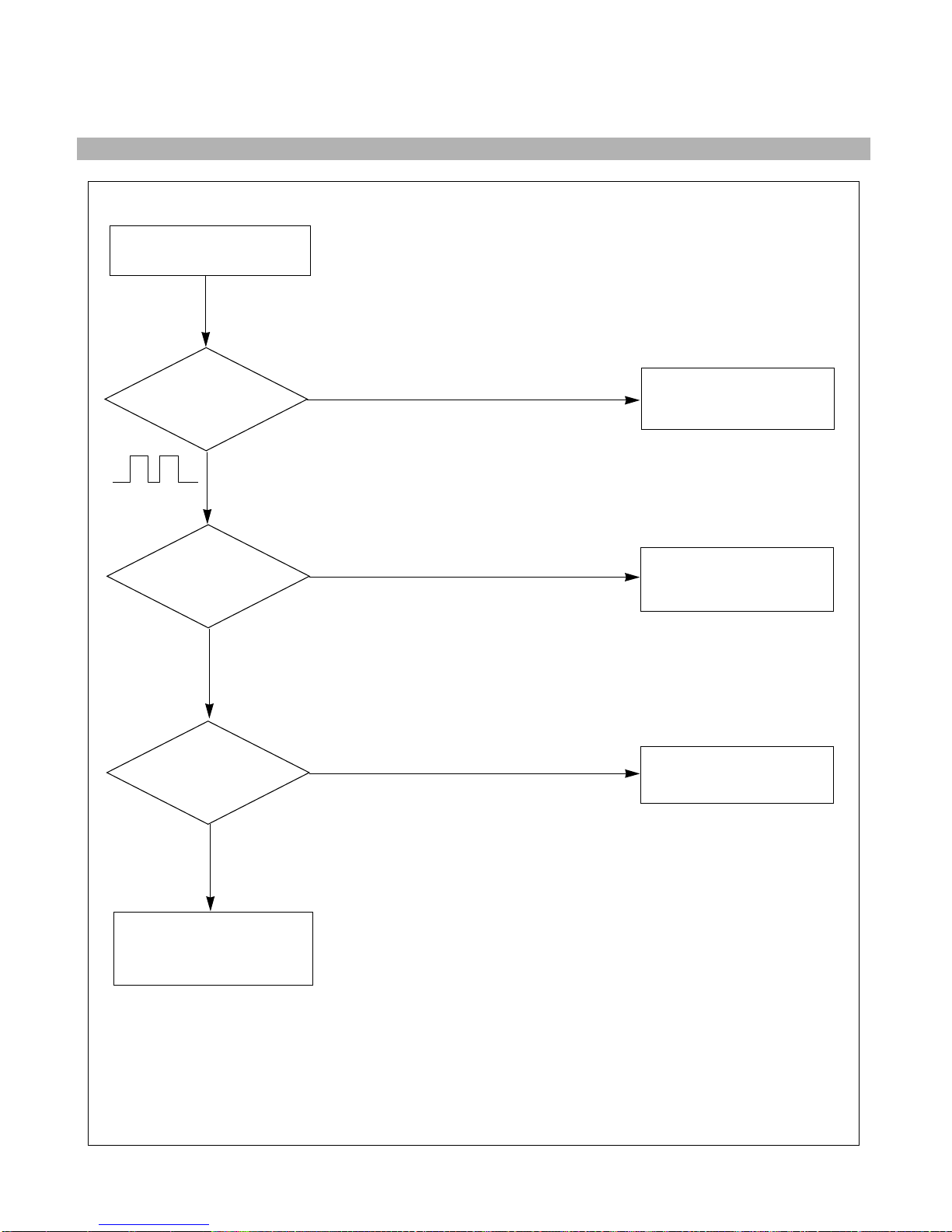
10. NO TILT (NO ROTATION)
NO TILT (NO ROTATION)
TROUBLE IN
IC401 (
MICOM)
TROUBLE IN
15V LINE, 6.3V LINE
TROUBLE IN
Q501~Q503
TROUBLE IN
P501, TILT COIL
NO
YES
YES
YES
CHECK
15V LINE
AND 6.3V LINE ?
CHECK
Q503 EMITTER
VOLTAGE ?
NO
NO
CHECK
IC401 PIN21
WAVE FORM ?
Page 23
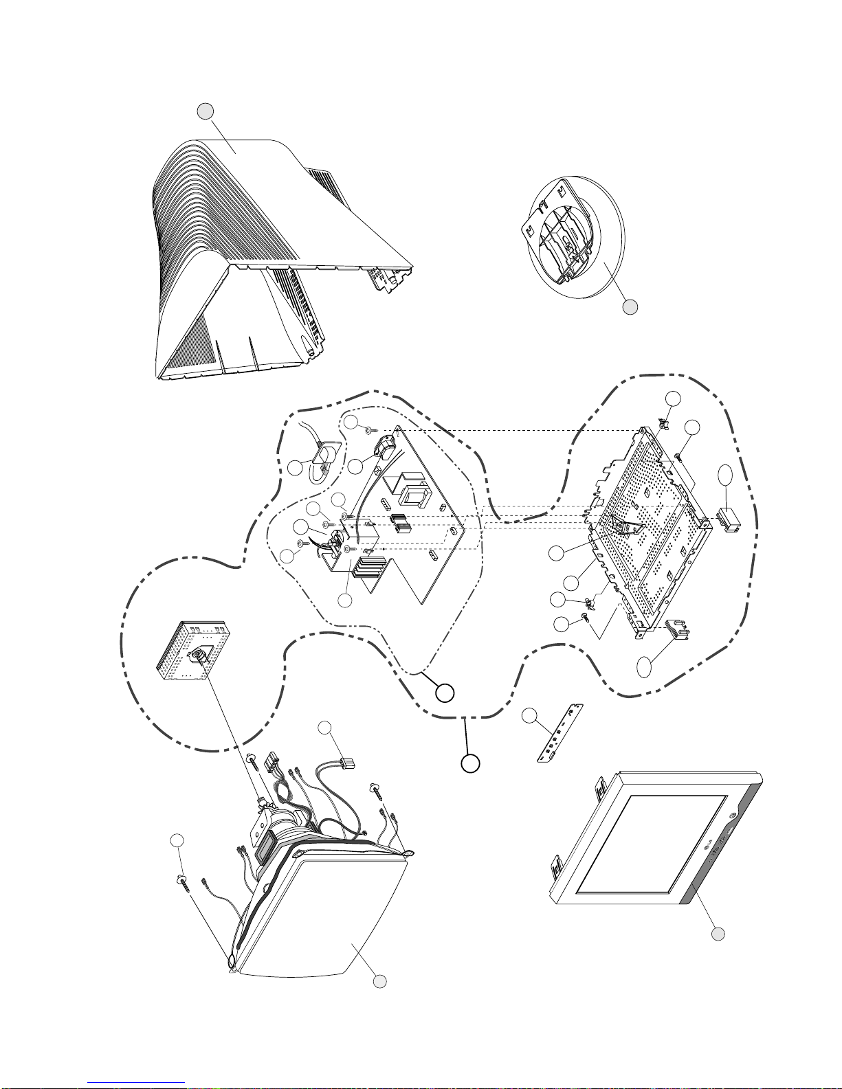
EXPLODED VIEW
- 23 -
11-1
12
12
14
8
7
B
A
15
9
6
5
4
3
a
b
b
d
c
10
13
11-2
14
2
MENU
SELECT
Brightview
1
Page 24
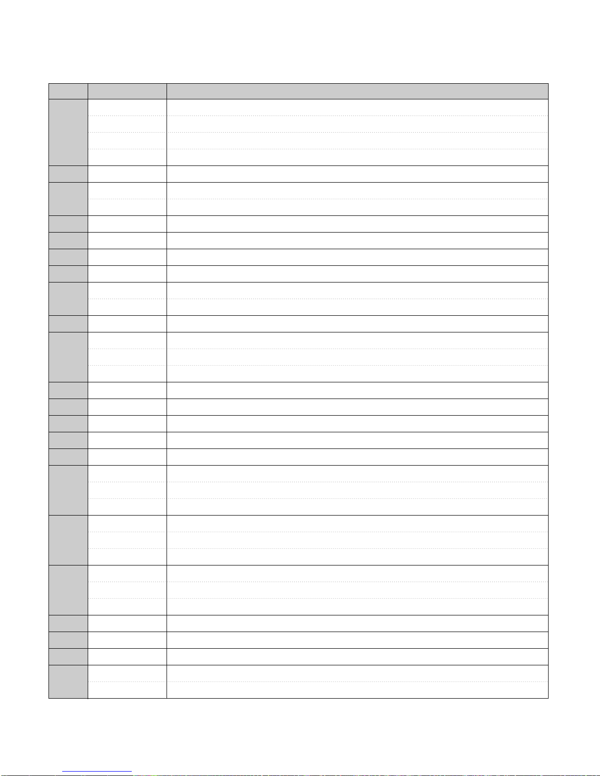
EXPLODED VIEW PARTS LIST
- 24 -
Description
CABINET ASSEMBLY, T710PH BRAND C079 5200HF,TCO99,B/VIEW,ER04,DI,SPRAY - For Europe
CABINET ASSEMBLY, E710PH BRAND C079 SILVER SPRAY - For Russia
C
ABINET ASSEMBLY, T710P BRAND C079 SPRAY,B/VIEW,LABEL CKD,ER04,5008HF - For Iran
CABINET ASSEMBLY, T710PH BRAND C079 TCO03,PC+ABS,ER04,B/VIEW,DI - For TCO03
CDT(CIRC), M41QEE903X 01NHUD LG-PHILIPS 85KHZ 29.1MM FLAT TCO HB
BACK COVER ASSEMBLY, T710BH/PH C046 GN5008HF,8C358(EQ54) - For Europe,
Iran
BACK COVER ASSEMBLY, E710BH 046 EQ54(8C358) - For Russia
TILT SWIVEL ASSEMBLY, E710BH T066 B60 HIPS
SCREW ASSEMBLY, TAPTITE P TYPE D5.0 L25.0 MSWR/FZMY .
COIL,DEGAUSSING, 75D-437 GET 0.4MM,120T,19 OHM,EB770F,WITH EARTH
FBT (FLY BACK TRANSFORMER), FQM17A007, TC710H(85K IBM) SAMSUNG 17”
SOCKET(CIRC), POWER, SA-4S HUA JIE AC UNIVERSAL 3PIN BLACK
SOCKET(CIRC), POWER, BAE EUN AC UNIVERSAL 3PIN BLACK
CABLE,D-SUB, UL20276-9C(5.8MM) AT 1560MM GRAY(85964) EB770H DM
METAL, SHIELD BOTTOM,CB553,0.8T,REAR HOLE DELETE
METAL, SHIELD BOTTOM,CB553H - For Russia
METAL SHIELD BOTTOM C-CKD - For Iran
BRACKET, CN771C SUPPORTER BOT.(RIGHT)
BRACKET, CN771C SUPPORTER BOT.(LEFT)
SCREW, PTP+4*20BP(MSWR/FZMY)
BRACKET, CB777H HOLDER FBT
HOLDER, PCB FIX , PC+ABS
PWB(PCB) ASSEMBLY,SUB, T710PHJ LGEDI CONTROL TOTAL BRAND CA-119
PWB(PCB) ASSEMBLY,SUB, T710BH CONTROL TOTAL BRAND CA-119 - For Russia
PWB(PCB) ASSEMBLY,SUB, T710PHJ CONTROL TOTAL IOMG CA-128 - For Iran
MAIN TOTAL ASSEMBLY, T710BHJ BRAND CA-128 LGEDI
MAIN TOTAL ASSEMBLY, T710PHJ BRAND CA-128 - For Russia
MAIN TOTAL ASSEMBLY, T710PHJ IOMG CA-128 - For Iran
PWB(PCB) ASSEMBLY,MAIN, T710PHJ KLEUED BRAND CA-128 LGEDI TOTAL
PWB(PCB) ASSEMBLY,MAIN, T710PHJ KLRDET BRAND CA-128 TOTAL - For Russia
PWB(PCB) ASSEMBLY,MAIN, T710PHJ KLIOEI IOMG CA-128 TOTAL - For Iran
SCREW,DRAWING, D3.5 L10.0 MSWR/FZMY +SW3.5+RW3.5
SCREW ASSEMBLY, TAPTITE P TYPE D3.0 L10.0 MSWR/FZMY SW3+RW10
SCREW,DRAWING, PZP+3*10(MSWR/FZMY)
SCREW, PVP+3*20(MSWR/FZMY)
SCREW, PVP+3*16(MSWR/FZMY) - For Russia
Part No.
3091TKC089V
3091TKC089B
3091TKC089M
3091TKC106F
6318L17014A
3809TKC050B
3809TKC050A
3043TKK108A
339-002K
6140TC3004B
6174T13010H
6620TKB002B
or 6620TKB002A
6850TA9009A
4950TKS155S
4950TKS207A
4950TKS212D
4810TKK150A
4810TKK151A
332-102F
4810TKK204A
4930TKK031C
6871TST370C
6871TST370A
6871TST370E
3313T17303C
3313T17303B
3313T17303E
6871TMT422C
6871TMT422B
6871TMT422E
332-112F
4001TKK004E
332-095B
332-113J
332-113H
Ref. No.
1
2
3
4
5
6
7
8
9
10
11-1
11-2
12
13
14
15
A
B
a
b
c
d
Page 25
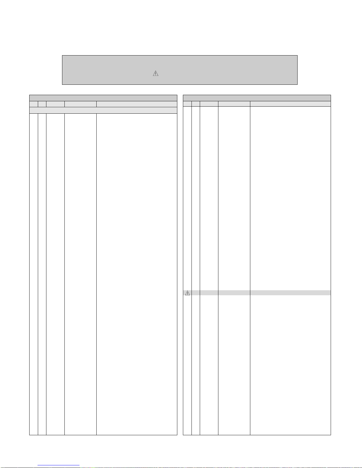
- 25 -
DATE: 2003. 06. 16.
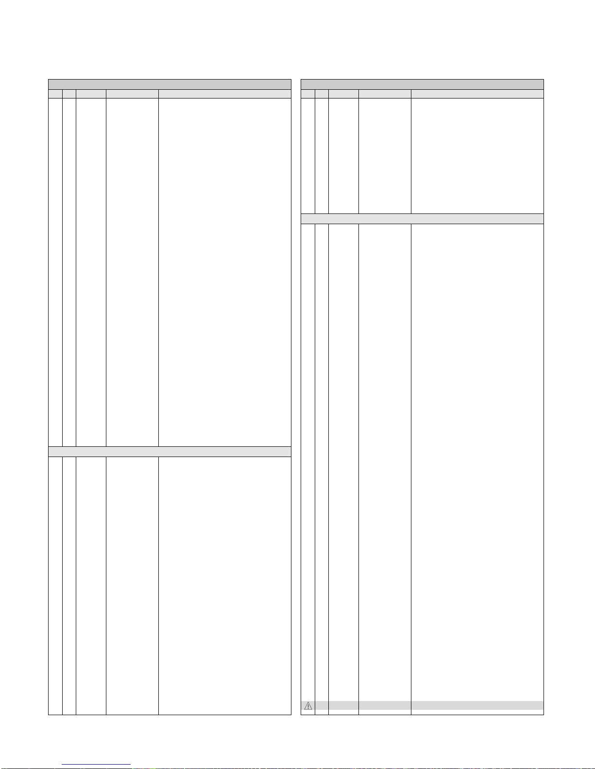
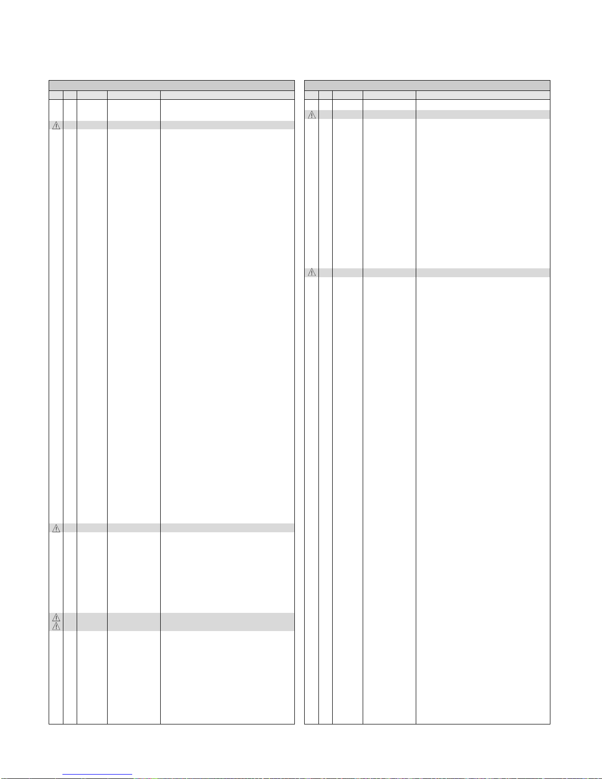
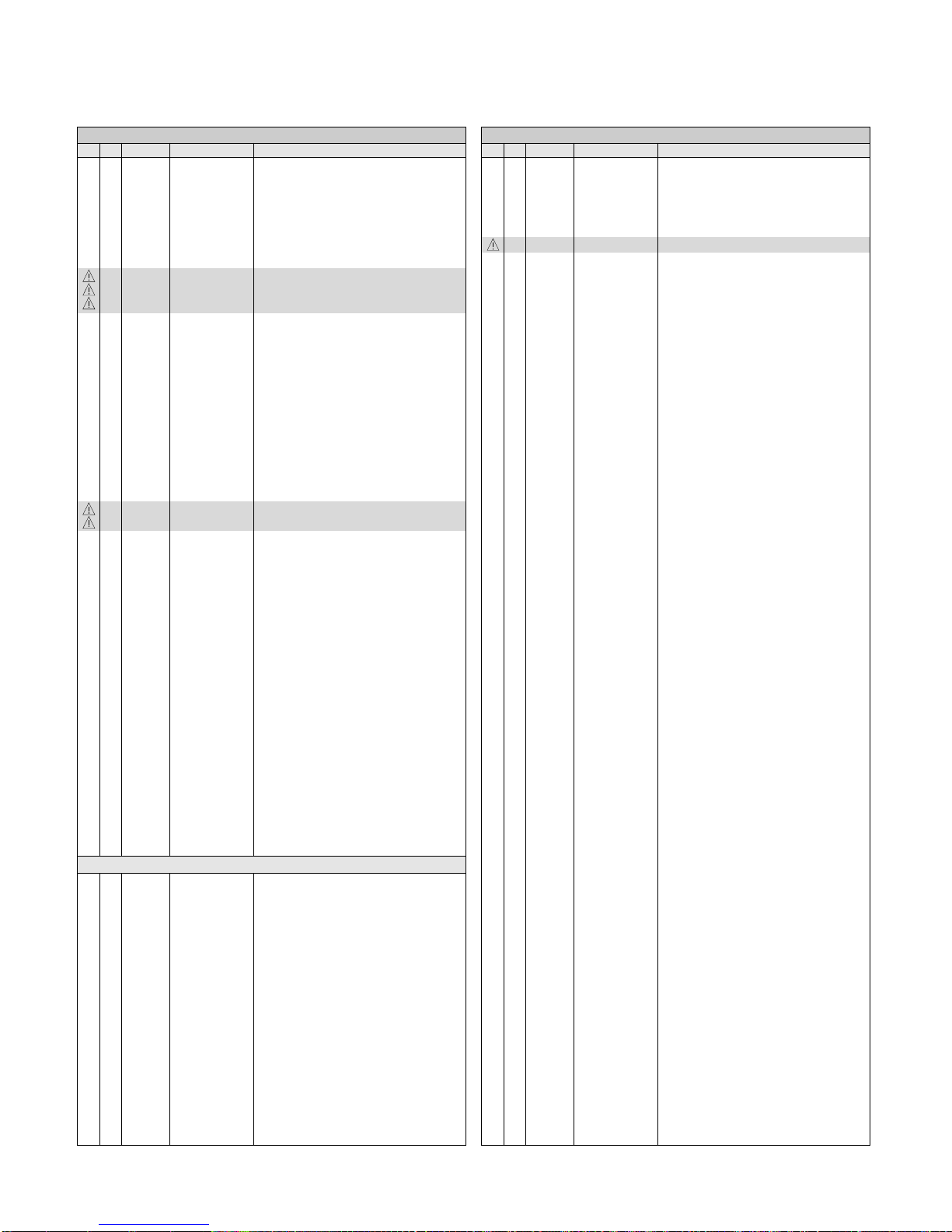
*S *AL LOC. NO. PART NO. DESCRIPTION / SPECIFICATION
C201 0CN1040K949 0.1M 50V Z F TA52
C301 0CQ1021N419 1000P 100V J POLY NI TP
C302 0CE106CF638 10UF SHL,SD 16V M FM5 TP 5
C303 0CN1020K519 1000P 50V K B TA52
C304 181-288B MKT 100V 104JTR PHS26104
C305 0CC2200W415 22PF 500V J NP0 TR
C306 0CZZTFT001W ECQB1H563JM3 563J 50V TP5.0
C307 0CK10301945 10000PF D 1KV Z F(Y5V) TR
C308 0CE107CF638 100UF SHL,SD 16V M FM5 TP 5
C309 0CK1040K945 0.1UF 50V Z F TR
C310 181-288B MKT 100V 104JTR PHS26104
C311 0CK4720K515 4700P 50V K B TS
C312 0CK4720K515 4700P 50V K B TS
C313 0CK4720K515 4700P 50V K B TS
C314 0CC4700W405 47PF 500V J SL TP
C315 0CE227CF638 220UF SHL,SD 16V M FM5 TP 5
C317 0CK1040K945 0.1UF 50V Z F TR
C318 0CK1040K945 0.1UF 50V Z F TR
C319 0CK1040K945 0.1UF 50V Z F TR
C321 0CE475CK638 4.7UF SHL,SD 50V M FM5 TP 5
C323 0CE476CF638 47UF SHL,SD 16V M FM5 TP 5
C324 0CK1040K945 0.1UF 50V Z F TR
C325 181-288B MKT 100V 104JTR PHS26104
C328 0CE476CN618 47UF SHL 100V M FL TP5
C330 181-288B MKT 100V 104JTR PHS26104
C331 181-288G MKT 100V 334JTR PHS26334
C332 181-288G MKT 100V 334JTR PHS26334
C333 181-288G MKT 100V 334JTR PHS26334
C334 181-288B MKT 100V 104JTR PHS26104
C335 181-288B MKT 100V 104JTR PHS26104
C339 0CK4710W515 470P 500V K B TS
C340 181-288B MKT 100V 104JTR PHS26104
C341 0CK10301945 10000PF D 1KV Z F(Y5V) TR
C344 181-288C MKT 100V 224JTR PHS 26224
C346 0CK10301945 10000PF D 1KV Z F(Y5V) TR
C372 0CK1040K945 0.1UF 50V Z F TR
C401 0CK1040K945 0.1UF 50V Z F TR
C402 0CE476CF638 47UF SHL,SD 16V M FM5 TP 5
C403 0CK1040K945 0.1UF 50V Z F TR
C406 0CK1010K515 100PF 50V K B TR
C407 0CK1010K515 100PF 50V K B TR
C408 0CK1040K945 0.1UF 50V Z F TR
C409 0CK1010K515 100PF 50V K B TR
C410 0CK1010K515 100PF 50V K B TR
C411 0CK1040K945 0.1UF 50V Z F TR
C412 0CK1040K945 0.1UF 50V Z F TR
C501 0CE106CF638 10UF SHL,SD 16V M FM5 TP 5
C599 0CE225CK638 2.2UF SHL,SD 50V M FM5 TP 5
C601 0CE477CH618 470UF SHL 25V M FL TP5
C602 181-288B MKT 100V 104JTR PHS26104
C603 0CE476EK638 47UF KMG 50V M FM5 TP 5
C604 0CZZTFT001Q ECQB1H183JM3 MATSUSHITA 50V
C605 0CK1020W515 1000P 500V K B TS
DATE: 2003. 06. 16.
*S *AL LOC. NO. PART NO. DESCRIPTION / SPECIFICATION
C701 0CQ3321N419 3300P 100V J POLY NI TP
C702 0CZZTFT001M ECQB1H103JF3 MATSUSHITA 50V
C703 0CZZTFT001Z ECQB1H104JM3 104J 50V TP5.0
C704 0CQ8221N519 0.0082U 100V K POLY NI TP
C706 0CZZTFT001Z ECQB1H104JM3 104J 50V TP5.0
C707 0CZZTFT002B ECQV1H154JZ3 154J 50V TP5.0
C708 0CE227CH638 220UF SHL,SD 25V M FM5 TP 5
C709 181-288P MKT 100V 153JTR PHS86153
C710 0CN1040K949 0.1M 50V Z F TA52
C711 0CQ5621N419 5600P 100V J POLY NI TP
C713 0CK2210K515 220P 50V K B TS
C714 0CE107CH638 100UF SHL,SD 25V M FM5 TP 5
C715 181-288N MKT 100V 103JTR PHS86103
C716 0CK2710K515 270P 50V K B TS
C717 0CZZTFT001R ECQB1H223JM3 223J 50V TP5.0
C718 181-288D MKT 100V 473JTR PHS26473
C719 0CZZTAB001F SHL-BP SYE / SWE 50V 3.3UF 2
C722 181-305Y MPP 250 204J S=10.0
C723 181-305K 564J 26.0*18.0*11.0*15.0 250
C724 0CK1040K945 0.1UF 50V Z F TR
C725 0CK6810W515 680P 500V K B TS
C726 181-305X 304J 19.0*18.5*10.5*10.0 250
C727 0CN1040K949 0.1M 50V Z F TA52
C728 0CQ5621N419 5600P 100V J POLY NI TP
C729 181-305Y MPP 250 204J S=10.0
C730 0CE105CK638 1UF SHL,SD 50V 20% FM5 TP 5
C731 181-309G 252J 23.0*16.0*10.0*15.0 1.6
C732 181-288N MKT 100V 103JTR PHS86103
C733 0CBZTBU003G 332J 20.0*11.5*7.0*10.0 800V
C734 0CE2266F618 22M SMS 16V M FM5 TP(5)
C736 181-309F 222J 23.0*15.5*9.5*15.0 1.6K
C737 0CK10102515 100PF D 2KV 10% B(Y5P) TR
C738 181-477Y 683JF 20.0*16.5*9.5*7.5 250V
C739 0CE106EK638 10UF KMG 50V M FM5 TP 5
C740 0CE337CL618 330UF SHL 63V M FL TP5
C741 0CZZTFT002B ECQV1H154JZ3 154J 50V TP5.0
C742 0CE105CN638 1UF SHL,SD 100V M FM5 TP 5
C743 0CZZTFT001R ECQB1H223JM3 223J 50V TP5.0
C744 0CZZTAB005B SMSHR SYE / SWE 200V 47UF 20
C745 0CK5610W515 560P 500V K B TS
C747 0CZZTFT002B ECQV1H154JZ3 154J 50V TP5.0
C748 0CK1510W515 150PF 500V K B TR
C749 0CE106CQ618 10UF SHL 200V M FL TP5
C750 0CK1040K945 0.1UF 50V Z F TR
C751 181-288J MKT 100V 563JTR PHS26563
C752 0CQ4721N419 0.0047U 100V J POLY NI TP5
C754 0CC4700W405 47PF 500V J SL TP
C767 0CK10301945 10000PF D 1KV Z F(Y5V) TR
C771 0CK10301945 10000PF D 1KV Z F(Y5V) TR
C774 181-288B MKT 100V 104JTR PHS26104
C781 0CK1030K945 0.01UF 50V Z F TR
C801 0CK1040K945 0.1UF 50V Z F TR
C805 0CE106CK638 10UF SHL,SD 50V M FM5 TP 5
C810 0CE106CK638 10UF SHL,SD 50V M FM5 TP 5
REPLACEMENT PARTS LIST
CAUTION: BEFORE REPLACING ANY OF THESE COMPONENTS,
READ CAREFULLY THE SAFETY PRECAUTIONS IN THIS MANUAL.
* NOTE : S SAFETY Mark
AL ALTERNATIVE PARTS
CAPACITORS
Page 26
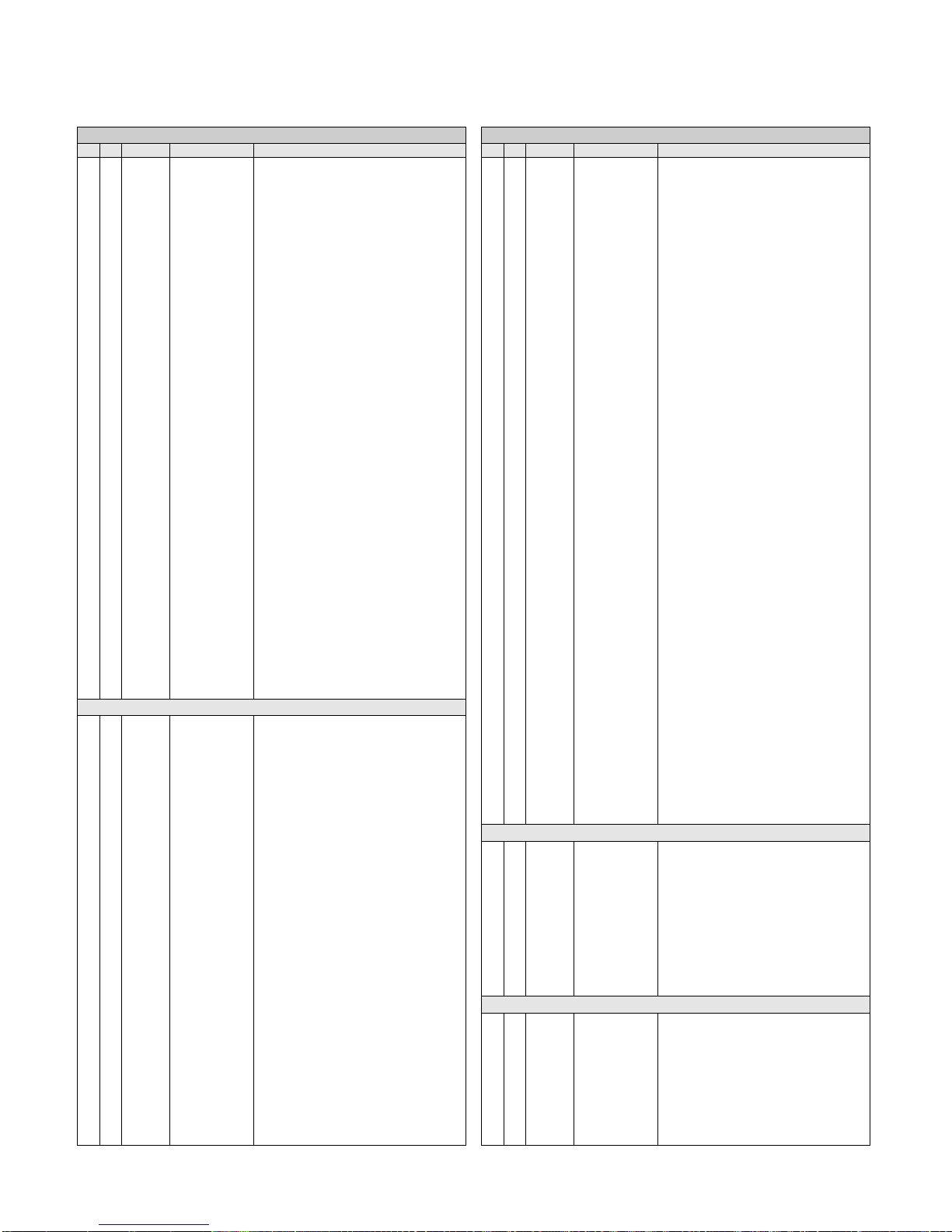
- 26 -
DATE: 2003. 06. 16.
*S *AL LOC. NO. PART NO. DESCRIPTION / SPECIFICATION
C821 0CK1040K945 0.1UF 50V Z F TR
C822 0CN1040K949 0.1M 50V Z F TA52
C830 0CK10102515 100PF D 2KV 10% B(Y5P) TR
C901 0CZZTFB001B BULK MPX 474K2YL (X2) BULK
C902 0CZZTFB001B BULK MPX 474K2YL (X2) BULK
C904 0CKZTBU003A
SC E 222M 10.0BW7 250V BK7.5 - For Europe
C904 0CZZTCB002A
DCF222M43Y5UQ7DK7D HONGMING - For Iran
C905 0CKZTBU003A
SC E 222M 10.0BW7 250V BK7.5
- For Europe
C905 0CZZTCB002A
DCF222M43Y5UQ7DK7D HONGMING - For Iran
C907 0CKZTBU003C
SC E 472M 14.0BW7 250V BK7.5
- For Europe
C907 0CZZTCB002C
DCF472M59Y5UQ7DK7D HONGMING - For Iran
C908 181-124R 220UF SMG(25.4*40) 400V M VN
C909 0CK10301510 0.01M 1KV K B S
C910 0CK33101515 330P 1KV K B TS
C911 0CE475CK638 4.7UF SHL,SD 50V M FM5 TP 5
C913 0CE476CK638 47UF SHL,SD 50V M FM5 TP 5
C914 0CZZTFT001P ECQB1H153JM3 153J 50V TP5.0
C915 0CK6810K515 680P 50V K B TS
C917 0CK1020K515 1000PF 50V K B TR
C918 0CN1040K949 0.1M 50V Z F TA52
C941 0CE108CD618 1000UF SHL 10V M FL TP5
C942 0CE107CF638 100UF SHL,SD 16V M FM5 TP 5
C943 0CK56101515 560P 1KV K B TS
C944 0CKZTBU003C
SC E 472M 14.0BW7 250V BK7.5
- For Europe
C944 0CZZTCB002C
DCF472M59Y5UQ7DK7D HONGMING - For Iran
C946 0CK1010W515 100P 500V K B TS
C951 0CE108CH630 1000UF SHL 25V M FM5 BULK
C952 0CE227CH638 220UF SHL,SD 25V M FM5 TP 5
C953 0CE107CF638 100UF SHL,SD 16V M FM5 TP 5
C954 0CE108CF630 1000UF SHL 16V M FM5 BULK
C971 0CE476CN618 47UF SHL 100V M FL TP5
C972 0CK1010W515 100P 500V K B TS
C999 0CE337EL630 330UF KMG 63V 20% BULK FM5
D201 0DL305029BA LTL-305DJ-0C2 TP LITEON GREE
D301 0DS141489AB 1N4148 TP GRANDE DO-34 500MW
D302 0DS141489AB 1N4148 TP GRANDE DO-34 500MW
D303 0DS141489AB 1N4148 TP GRANDE DO-34 500MW
D304 0DS141489AB 1N4148 TP GRANDE DO-34 500MW
D305 0DS141489AB 1N4148 TP GRANDE DO-34 500MW
D306 0DS141489AB 1N4148 TP GRANDE DO-34 500MW
D307 0DS124409AA 1SS244 TP ROHM KOREA
D308 0DS124409AA 1SS244 TP ROHM KOREA
D309 0DS124409AA 1SS244 TP ROHM KOREA
D310 0DS124409AA 1SS244 TP ROHM KOREA
D311 0DS124409AA 1SS244 TP ROHM KOREA
D312 0DS124409AA 1SS244 TP ROHM KOREA
D313 0DS124409AA 1SS244 TP ROHM KOREA
D314 0DS124409AA 1SS244 TP ROHM KOREA
D315 0DS124409AA 1SS244 TP ROHM KOREA
D402 0DS141489AB 1N4148 TP GRANDE DO-34 500MW
D404 971-0016 TIN HDC 0.60H
D512 0DS141489AB 1N4148 TP GRANDE DO-34 500MW
D702 0DS141489AB 1N4148 TP GRANDE DO-34 500MW
D704 0DR150051AA DMV1500M/F5 ST SGS-THOMSON T
D705 0DRGF00069A SB140 GULF TP DO41 40V 1A 40
D706 0DR150001AA DTV1500MFP ST SGS-THOMSON TO
D709 971-0016 TIN HDC 0.60H
D710 0DR400409AC UF4004 GULF TP DO41 400V 1A
D711 0DS141489AB 1N4148 TP GRANDE DO-34 500MW
DATE: 2003. 06. 16.
*S *AL LOC. NO. PART NO. DESCRIPTION / SPECIFICATION
D712 0DR100009CA RGP10G TP GULF SEMICONDUCTOR
D714 0DS141489AB 1N4148 TP GRANDE DO-34 500MW
D715 0DS141489AB 1N4148 TP GRANDE DO-34 500MW
D716 0DR140059AD 1N4005 GULF TP DO41 600V 1A
D717 0DR140059AD 1N4005 GULF TP DO41 600V 1A
D718 0DR140059AD 1N4005 GULF TP DO41 600V 1A
D719 0DR100009DA RGP10J TP GULF SEMICONDUCTOR
D720 0DS141489AB 1N4148 TP GRANDE DO-34 500MW
D721 0DS141489AB 1N4148 TP GRANDE DO-34 500MW
D722 0DS141489AB 1N4148 TP GRANDE DO-34 500MW
D723 0DS141489AB 1N4148 TP GRANDE DO-34 500MW
D724 0DR140059AD 1N4005 GULF TP DO41 600V 1A
D730 0DS141489AB 1N4148 TP GRANDE DO-34 500MW
D731 0DS141489AB 1N4148 TP GRANDE DO-34 500MW
D768 0DR100009DA RGP10J TP GULF SEMICONDUCTOR
D801 0DS141489AB 1N4148 TP GRANDE DO-34 500MW
D802 0DS141489AB 1N4148 TP GRANDE DO-34 500MW
D821 0DS141489AB 1N4148 TP GRANDE DO-34 500MW
D900 0DRTW00071A TS4B05G-1021 TIWAN SEMI ST N
D902 0DR153979AA 1N5397GP TP G.I DO201AD 600V
D904 0DR100009CA RGP10G TP GULF SEMICONDUCTOR
D905 0DD400709CB UF4007 TP G.I DO204AL 1000V
D906 0DR100009CA RGP10G TP GULF SEMICONDUCTOR
D908 0DS141489AB 1N4148 TP GRANDE DO-34 500MW
D910 0DS141489AB 1N4148 TP GRANDE DO-34 500MW
D911 0DS141489AB 1N4148 TP GRANDE DO-34 500MW
D941 0DR100009LD
UG1D GULF TP DO41 200V 1A 40
- For Europe
D941 0DR100009LA UG1D TP G.I DO204AL 200V 1A - For Iran
D942 0DRGS00089A SB1H100 GENERAL SEMICONDUCTO
D951 0DR540400AA UF5404L BK G.I DO201AD 400V
D952 0DS141489AB 1N4148 TP GRANDE DO-34 500MW
D961 0DRTW00060A SF38GL-1121 TIWAN SEMI BK DO
D962 0DRTW00060A SF38GL-1121 TIWAN SEMI BK DO
D971 0DR100009DA RGP10J TP GULF SEMICONDUCTOR
ZD402 0DZ560009AG GDZJ5.6B TP GRANDE DO-34 500
ZD403 0DZ560009AG GDZJ5.6B TP GRANDE DO-34 500
ZD404 0DZ560009AG GDZJ5.6B TP GRANDE DO-34 500
ZD405 0DZ560009AG GDZJ5.6B TP GRANDE DO-34 500
ZD407 0DZ560009AG GDZJ5.6B TP GRANDE DO-34 500
ZD701 0DZ120009BF GDZJ12B TP GRANDE DO34 0.5W
ZD902 0DZ510009BE GDZ5.1B TP GRANDE DO34 500MW
IC302 0IPRPNS025A LM1246DDA/NA NATIONAL SEMICO
IC303 0IPRPNS026A LM2445TA NATIONAL SEMICONDUC
IC304 0IPRPNS005A LM2480NA NATIONAL SEMICONDUC
IC401 0IZZTSZ266A SS 42PIN ST OTP 6KEY T710PJ
IC402 0ISG240860A M24C08-BN6 8DIP BK 8K SERIAL
IC601 0IPRPPH018A TDA4867J PHILIPS 9PIN,ST DIP
IC701 0IPRPPH005A TDA4841PS PHILIPS 32P,SDIP S
IC901 0ISS384200A KA3842B (PWM)
FB201 6210TCE003J BAS2550T BO SUNG 2550MM AXIA
FB301 6210TCE003J BAS2550T BO SUNG 2550MM AXIA
FB302 6210TCE003J BAS2550T BO SUNG 2550MM AXIA
FB303 6210TCE003J BAS2550T BO SUNG 2550MM AXIA
FB304 6210TCE003J BAS2550T BO SUNG 2550MM AXIA
FB305 6210TCE003P BRS2550B BO SUNG 2550MM RADI
FB306 6210TCZ001J BAS3550T0(125-022J) BO SUNG
DIODEs
ICs
COILs & COREs
Page 27
DATE: 2003. 06. 16.
*S *AL LOC. NO. PART NO. DESCRIPTION / SPECIFICATION
FB307 6210TCZ001J BAS3550T0(125-022J) BO SUNG
FB308 6210TCZ001J BAS3550T0(125-022J) BO SUNG
FB309 6210TCE003J BAS2550T BO SUNG 2550MM AXIA
FB310 6210TCE003A BRD3510B BO SUNG 3510MM RADI
FB311 6210TCE003J BAS2550T BO SUNG 2550MM AXIA
FB312 6210TCE003J BAS2550T BO SUNG 2550MM AXIA
FB313 6210TCE003P BRS2550B BO SUNG 2550MM RADI
FB401 6210TCE003J BAS2550T BO SUNG 2550MM AXIA
FB402 6210TCE003L BAS3580T BO SUNG 3580MM AXIA
FB403 6210TCE003J BAS2550T BO SUNG 2550MM AXIA
FB501 6210TCE003J BAS2550T BO SUNG 2550MM AXIA
FB502 6210TCE003J BAS2550T BO SUNG 2550MM AXIA
FB701 6210TCE003L BAS3580T BO SUNG 3580MM AXIA
FB702 6210TCE003H BAS3510T BO SUNG 3510MM AXIA
FB703 6210TCE003B BRS3580B BO SUNG 3580MM RADI
FB704 6210TCE003H BAS3510T BO SUNG 3510MM AXIA
FB705 6210TCE003L BAS3580T BO SUNG 3580MM AXIA
FB706 6210TCE003H BAS3510T BO SUNG 3510MM AXIA
FB902 6210TCE003J BAS2550T BO SUNG 2550MM AXIA
FB904 6210TCE003K BAS3550T BO SUNG 3550MM AXIA
FB921 6210TCE003A BRD3510B BO SUNG 3510MM RADI
FB922 6210TCE003L BAS3580T BO SUNG 3580MM AXIA
FB951 6210TCE003J BAS2550T BO SUNG 2550MM AXIA
FB952 6210TCE003G BRS3550B BO SUNG 3550MM RADI
L302 971-0016 TIN HDC 0.60H
L303 971-0016 TIN HDC 0.60H
L311 0LA0680K119 0.68UH K 2.3*3.4 TP
L312 0LA0680K119 0.68UH K 2.3*3.4 TP
L313 0LA0680K119 0.68UH K 2.3*3.4 TP
L702 6140TBZ025A DR14*20 120UH 0.12*25MM 47.5
L703 6140TYZ011G - GET DR14*25,4.0UH,EB770H
L705 6140TBZ026C DR15*18-C9.8 100UH 0.1*30MM
L901 6200TZZ004A SQE2626 NAMYANG BK L/FILTER
L903 6200J00003A RH3.5*5.0 BOSUNG TP
Q501 0TR320209AA KTC3202-Y(KTC1959) TP KEC TO
Q502 0TR127009AA KTA1270-Y(KTA562TM) TP KEC T
Q503 0TR319809AA KTC3198-Y(KTC1815) TP KEC TO
Q705 0TR200009AB KTC200-Y TP KEC TO92 NPN
Q706 0TRFC10007A FJAF6815 FAIRCHILD ST TO3PF
Q707 0TR127009AA KTA1270-Y(KTA562TM) TP KEC T
Q708 0TR127009AA KTA1270-Y(KTA562TM) TP KEC T
Q709 0TR141300AB KTD1413 BK KEC TO220I S NPN
Q710 0TRKE90020A MPSA44 KEC TP TO92 500V 300M
Q711 0TF630000DA IRF630A BK SAMSUNG 200V 9A T
Q712 4921TKK391Q - T003A T710PHJ LGEDI
- For Europe
Q712 4921TKK391K - T003A IRF630A TC170H - For Iran
Q713 4921TKK391Q - T003A T710PHJ LGEDI
Q714 0TR319809AA KTC3198-Y(KTC1815) TP KEC TO
Q715 0TR319809AA KTC3198-Y(KTC1815) TP KEC TO
Q716 0TR319809AA KTC3198-Y(KTC1815) TP KEC TO
Q717 0TR100809AA KSC1008C-Y TP SAMSUNG TO92
Q719 0TF630000CA IRFS630A BK SAMSUNG 200V 6.5
Q720 0TR390409CA FAIRCHILD 2N3904(TA) TP TO-9
Q722 0TR319809AA KTC3198-Y(KTC1815) TP KEC TO
Q723 0TR127009AA KTA1270-Y(KTA562TM) TP KEC T
Q731 0TR928009AB KSA928A-Y TP SAMSUNG TO92L P
Q732 0TR319809AA KTC3198-Y(KTC1815) TP KEC TO
Q799 0TRKE90019A MPSA92 KEC TP TO92 -300V -50
DATE: 2003. 06. 16.
*S *AL LOC. NO. PART NO. DESCRIPTION / SPECIFICATION
Q821 0TRKE10007A
KTD882-Y KEC ST TO126 40V 3A
- For Europe
Q821 0TRFC10003A FAIRCHILD KSD882Y-S ST TO126 - For Iran
Q901 0TFFN10003C INFINEON SPA07N60C3(E8153) S
Q903 0TRKE10007A
KTD882-Y KEC ST TO126 40V 3A
- For Europe
Q903 0TRFC10003A FAIRCHILD KSD882Y-S ST TO126 - For Iran
Q941 0TR319809AA KTC3198-Y(KTC1815) TP KEC TO
Q942 0TR928009AB KSA928A-Y TP SAMSUNG TO92L P
Q951 0TR319809AA KTC3198-Y(KTC1815) TP KEC TO
Q952 0TR928009AB KSA928A-Y TP SAMSUNG TO92L P
Q953 0TR319809AA KTC3198-Y(KTC1815) TP KEC TO
R201 0RD1001Q609 1K 1/4W(3 5% TA52
R202 0RD0912Q609 91 OHM 1/4 W (3.4) 5% TA52
R203 0RD2200Q609 220 1/4W(3 5% TA52
R204 0RD4300Q609 430 OHM 1/4 W(3.4) 5.00% TA5
R205 0RD1001Q609 1K 1/4W(3 5% TA52
R206 0RD0912Q609 91 OHM 1/4 W (3.4) 5% TA52
R207 0RD4300Q609 430 OHM 1/4 W(3.4) 5.00% TA5
R208 0RD2200Q609 220 1/4W(3 5% TA52
R209 0RD9100Q609 910 1/4W(3 5% TA52
R210 0RD2200Q609 220 1/4W(3 5% TA52
R211 0RD2200Q609 220 1/4W(3 5% TA52
R301 0RD0752Q609 75 1/4W(3 5% TA52
R302 0RD0752Q609 75 1/4W(3 5% TA52
R303 0RD0752Q609 75 1/4W(3 5% TA52
R305 0RN4701F409 4.70K 1/6W 1% TA52
R314 0RD1000Q609 100 1/4W(3 5% TA52
R315 0RD1000Q609 100 1/4W(3 5% TA52
R319 0RD4701Q609 4.70K 1/4W(3 5% TA52
R320 0RD4701Q609 4.70K 1/4W(3 5% TA52
R326 0RD2201Q609 2.20K 1/4W(3 5% TA52
R327 0RD1001Q609 1K 1/4W(3 5% TA52
R328 0RD1001Q609 1K 1/4W(3 5% TA52
R329 0RD1001Q609 1K 1/4W(3 5% TA52
R330 971-0016 TIN HDC 0.60H
R331 0RD1500Q609 150 1/4W(3 5% TA52
R332 0RD1500Q609 150 1/4W(3 5% TA52
R333 0RD1300Q609 130 1/4W(3 5% TA52
R334 0RD3303Q609 330K 1/4W(3 5% TA52
R335 0RD3303Q609 330K 1/4W(3 5% TA52
R336 0RD3303Q609 330K 1/4W(3 5% TA52
R337 0RD3000Q609 300 1/4W(3 5% TA52
R340 0RN1002F409 10K 1/6W 1 TA52
R341 0RD0332A609 33 OHM 1/2 W (7.0) 5% TA52
R342 0RD0332A609 33 OHM 1/2 W (7.0) 5% TA52
R343 0RD0332A609 33 OHM 1/2 W (7.0) 5% TA52
R344 0RD0332Q609 33 1/4W(3 5% TA52
R345 0RD0332Q609 33 1/4W(3 5% TA52
R346 0RD0332Q609 33 1/4W(3 5% TA52
R347 0RD1200Q609 120 1/4W(3 5% TA52
R401 0RD1000Q609 100 1/4W(3 5% TA52
R402 0RD5600Q609 560 1/4W(3 5% TA52
R403 0RD1002Q609 10K 1/4W(3 5% TA52
R404 0RD1001Q609 1K 1/4W(3 5% TA52
R405 0RD2001Q609 2K 1/4W(3 5% TA52
R406 0RD2001Q609 2K 1/4W(3 5% TA52
R407 0RD1300Q609 130 1/4W(3 5% TA52
R408 0RD1300Q609 130 1/4W(3 5% TA52
R409 0RD1000Q609 100 1/4W(3 5% TA52
R411 0RD3901Q609 3.90K 1/4W(3 5% TA52
- 27 -
RESISTORs
TRANSISTORs
Page 28
- 28 -
DATE: 2003. 06. 16.
*S *AL LOC. NO. PART NO. DESCRIPTION / SPECIFICATION
R412 0RD1004Q609 1M OHM 1/4 W (3.4) 5% TA52
R415 0RD1001Q609 1K 1/4W(3 5% TA52
R416 0RD4701Q609 4.70K 1/4W(3 5% TA52
R417 0RD1000Q609 100 1/4W(3 5% TA52
R418 0RD1002Q609 10K 1/4W(3 5% TA52
R419 0RD1004Q609 1M OHM 1/4 W (3.4) 5% TA52
R420 0RD2001Q609 2K 1/4W(3 5% TA52
R424 0RD2200Q609 220 1/4W(3 5% TA52
R425 0RD4701Q609 4.70K 1/4W(3 5% TA52
R426 0RD4701Q609 4.70K 1/4W(3 5% TA52
R429 0RD1000Q609 100 1/4W(3 5% TA52
R430 0RD1000Q609 100 1/4W(3 5% TA52
R431 0RD1000Q609 100 1/4W(3 5% TA52
R432 0RD1000Q609 100 1/4W(3 5% TA52
R433 0RD1000Q609 100 1/4W(3 5% TA52
R434 0RD1000Q609 100 1/4W(3 5% TA52
R438 0RD1001Q609 1K 1/4W(3 5% TA52
R439 0RD1001Q609 1K 1/4W(3 5% TA52
R445 0RD2201Q609 2.20K 1/4W(3 5% TA52
R446 0RD1002Q609 10K 1/4W(3 5% TA52
R447 0RD1001Q609 1K 1/4W(3 5% TA52
R448 0RD1801Q609 1.80K 1/4W(3 5% TA52
R501 0RD0102A609 10 OHM 1/2 W (7.0) 5% TA52
R508 0RD4702Q609 47K 1/4W(3 5% TA52
R515 0RD1502Q609 15K 1/4W(3 5% TA52
R597 0RD3902Q609 39K 1/4W(3 5% TA52
R598 0RD5601Q609 5.60K 1/4W(3 5% TA52
R599 0RD0202A609 20 OHM 1/2 W (7.0) 5% TA52
R601 0RD1001Q609 1K 1/4W(3 5% TA52
R602 0RD1001Q609 1K 1/4W(3 5% TA52
R603 0RN0390H609 0.39 1/2W 5 TA52
R604 0RD0101A609 1 OHM 1/2 W (7.0) 5% TA52
R605 0RD0912A609 91 OHM 1/2 W (7.0) 5% TA52
R606 0RD1000A609 100 OHM 1/2 W (7.0) 5% TA52
R607 0RN4301F409 4.30K 1/6W 1% TA52
R608 0RD3300A609 330 OHM 1/2 W (7.0) 5% TA52
R610 0RD1101Q609 1.1K OHM 1/4 W (3.4) 5% TA52
R613 0RD1801Q609 1.80K 1/4W(3 5% TA52
R700 971-0016 TIN HDC 0.60H
R701 0RN3301F409 3.30K 1/6W 1% TA52
R702 0RN7500F409 750 1/6W 1% TA52
R703 0RD1001Q609 1K 1/4W(3 5% TA52
R704 0RD3601Q509 3.6K OHM 1/4 W(3.4) 2% TA52
R705 0RD4701Q609 4.70K 1/4W(3 5% TA52
R706 0RN2701F409 2.7K OHM 1/6 W 1.00% TA52
R709 0RD2202Q609 22K 1/4W(3 5% TA52
R710 0RD1000Q609 100 1/4W(3 5% TA52
R711 0RD1000Q609 100 1/4W(3 5% TA52
R712 0RD1501Q609 1.50K 1/4W(3 5% TA52
R713 0RD1000Q609 100 1/4W(3 5% TA52
R714 0RD5601Q609 5.60K 1/4W(3 5% TA52
R714-1 0RN3001F409 3K 1/6W 1% TA52
R714-2 0RN1201F409 1.20K 1/6W 1% TA52
R715 0RD7502Q609 75K 1/4W(3 5% TA52
R717 0RD1002Q609 10K 1/4W(3 5% TA52
R718 0RD1602Q609 16K 1/4W(3 5% TA52
R719 971-0016 TIN HDC 0.60H
R720 0RC1205Q609 12M OHM 1/4 W(3.4) 5% TA52
R721 0RD1001Q609 1K 1/4W(3 5% TA52
R722 0RD4301Q609 4.30K 1/4W(3 5% TA52
R723 0RD1001Q609 1K 1/4W(3 5% TA52
R724 0RD1001Q609 1K 1/4W(3 5% TA52
DATE: 2003. 06. 16.
*S *AL LOC. NO. PART NO. DESCRIPTION / SPECIFICATION
R725 0RN1501F409 1.5K 1/6W 1 TA52
R726 0RD5102A609 51K OHM 1/2 W (7.0) 5% TA52
R727 0RX0562K665 56 OHM 2 W 5.00% SF
R728 0RD1001Q609 1K 1/4W(3 5% TA52
R729 0RD1002Q609 10K 1/4W(3 5% TA52
R731 0RD1002Q609 10K 1/4W(3 5% TA52
R732 0RD6802Q509 68K OHM 1/4 W (3.4) 2% TA52
R733 0RD1002Q609 10K 1/4W(3 5% TA52
R735 0RD1001Q609 1K 1/4W(3 5% TA52
R736 0RX2201J609 2.2KOHM 1 W 5% TA52
R737 0RN0560H609 0.56 1/2W 5 TA52
R738 0RN0560H609 0.56 1/2W 5 TA52
R739 0RD6800Q609 680 1/4W(3 5% TA52
R740 0RD0271A609 2.7 OHM 1/2 W (7.0) 5% TA52
R741 0RD1000Q609 100 1/4W(3 5% TA52
R742 0RD2702Q509 27K OHM 1/4 W(3.4) 2% TA52
R743 0RD2702Q509 27K OHM 1/4 W(3.4) 2% TA52
R744 0RX2200K607 220 OHM 2 W 5% TA62
R745 0RD4702Q609 47K 1/4W(3 5% TA52
R746 0RD2201Q609 2.20K 1/4W(3 5% TA52
R747 0RD3001Q609 3K 1/4W(3 5% TA52
R748 0RD4702Q609 47K 1/4W(3 5% TA52
R749 0RD2201Q609 2.20K 1/4W(3 5% TA52
R750 0RD3001Q609 3K 1/4W(3 5% TA52
R751 0RD0222A609 22 OHM 1/2 W (7.0) 5% TA52
R752 0RD2201Q609 2.20K 1/4W(3 5% TA52
R753 0RD3001Q609 3K 1/4W(3 5% TA52
R754 0RX4300K607 430 OHM 2 W 5% TA62
R755 0RD0471Q609 4.70 1/4W(3 5% TA52
R756 0RD2202A609 22K OHM 1/2 W (7.0) 5% TA52
R757 971-0016 TIN HDC 0.60H
R758 0RN1303F409 130K 1/6W 1% TA52
R759 0RD9101Q509 9100 OHM 1/4 W(3.4) 2% TA52
R760 0RD5103Q609 510K 1/4W(3 5% TA52
R761 0RD3001Q609 3K 1/4W(3 5% TA52
R762 0RD3001Q609 3K 1/4W(3 5% TA52
R763 0RD3001Q609 3K 1/4W(3 5% TA52
R764 971-0016 TIN HDC 0.60H
R765 0RD1800A609 180 OHM 1/2 W (7.0) 5% TA52
R766 0RD2201A609 2.2K OHM 1/2 W (7.0) 5% TA52
R767 971-0016 TIN HDC 0.60H
R768 0RD9103A609 910K OHM 1/2 W (7.0) 5% TA52
R769 0RN3901F409 3.90K 1/6W 1% TA52
R771 0RD1101A609 1.1K OHM 1/2 W (7.0) 5% TA52
R772 0RD2402A609 24K OHM 1/2 W (7.0) 5% TA52
R773 0RD1003A609 100K OHM 1/2 W (7.0) 5% TA52
R778 0RD2001Q609 2K 1/4W(3 5% TA52
R779 0RD3001Q509 3000 OHM 1/4 W(3.4) 2% TA52
R781 0RD5601Q609 5.60K 1/4W(3 5% TA52
R782 0RD3301A609 3.3K OHM 1/2 W(7.0) 5.00% TA
R783 971-0016 TIN HDC 0.60H
R784 0RD1000Q609 100 1/4W(3 5% TA52
R786 0RD2002Q609 20K 1/4W(3 5% TA52
R787 0RD0472A609 47 OHM 1/2 W (7.0) 5% TA52
R790 0RD1502Q609 15K 1/4W(3 5% TA52
R793 0RD4702Q609 47K 1/4W(3 5% TA52
R797 0RD1501Q609 1.50K 1/4W(3 5% TA52
R798 0RD2001Q609 2K 1/4W(3 5% TA52
R799 0RD1502Q609 15K 1/4W(3 5% TA52
R801 0RD1802Q609 18K 1/4W(3 5% TA52
R802 0RD1502Q609 15K 1/4W(3 5% TA52
R803 0RD2001Q609 2K 1/4W(3 5% TA52
Page 29
DATE: 2003. 06. 16.
*S *AL LOC. NO. PART NO. DESCRIPTION / SPECIFICATION
R805 0RD2001Q609 2K 1/4W(3 5% TA52
R806 0RD4702Q609 47K 1/4W(3 5% TA52
R808 0RN7502F409 75000 OHM 1/6 W 1% TA52
R809 0RX0151L665 1.5 OHM 3 W 5% SF
R813 0RD6802A609 68K OHM 1/2 W (7.0) 5% TA52
R814 0RD2002Q609 20K 1/4W(3 5% TA52
R816 0RN3301F409 3.30K 1/6W 1% TA52
R818 0RN6202F409 62KOHM 1/6 W 1% TA52
R819 0RN8202F409 82K 1/6W 1% TA52
R821 0RD3001Q609 3K 1/4W(3 5% TA52
R822 0RX0152J609 15 OHM 1 W 5% TA52
R823 0RX0432K665 43OHM 2 W 5% SF
R831 0RD1002Q609 10K 1/4W(3 5% TA52
R901 0RD4703A609 470K OHM 1/2 W (7.0) 5% TA52
R902 0RD0332Q609 33 1/4W(3 5% TA52
R904 0RX3902K665 39K OHM 2 W 5% SF
R906 0RD6200Q609 620 1/4W(3 5% TA52
R908 0RN0220H609 0.22 1/2W 5% TA52
R909 0RN0220H609 0.22 1/2W 5% TA52
R910 0RX4702J609 47K OHM 1 W 5% TA52
R911 0RD0362Q609 36 OHM 1/4 W(3.4) 5.00% TA52
R912 0RD1802Q609 18K 1/4W(3 5% TA52
R913 0RD2201Q609 2.20K 1/4W(3 5% TA52
R915 0RD1200Q609 120 1/4W(3 5% TA52
R916 0RD1002Q609 10K 1/4W(3 5% TA52
R918 0RD1001Q609 1K 1/4W(3 5% TA52
R923 0RD1003Q609 100K 1/4W(3 5% TA52
R925 0RB0150K607 0.15 OHM 2 W 5% TA62
R926 0RD5101Q609 5.10K 1/4W(3 5% TA52
R927 0RD2002Q609 20K 1/4W(3 5% TA52
R928 0RD1800Q609 180 1/4W(3 5% TA52
R929 0RD0332Q609 33 1/4W(3 5% TA52
R941 0RN0220H609 0.22 1/2W 5% TA52
R944 0RD4700A609 470 OHM 1/2 W (7.0) 5% TA52
R945-1 0RD4701Q609 4.70K 1/4W(3 5% TA52
R951 0RN0101H609 1.0 1/2W 5 TA52
R952 0RD1202A609 12K OHM 1/2 W(7.0) 5.00% TA5
R953 0RD1001A609 1K OHM 1/2 W (7.0) 5% TA52
R954 0RD4701Q609 4.70K 1/4W(3 5% TA52
R955 0RD4701Q609 4.70K 1/4W(3 5% TA52
R956 0RD6802A609 68K OHM 1/2 W (7.0) 5% TA52
R957 0RD0472A609 47 OHM 1/2 W (7.0) 5% TA52
R960 0RD6200A609 620 OHM 1/2 W(7.0) 5.00% TA5
F1 430-858C AFC-520 BAE EUN TA
F2 430-858C AFC-520 BAE EUN TA
F901 0FZZTTH004B TIME LAG HBC TSC 5A/250V,WAL
RL901 6920TBB006A DY3M-DC12V DONGYANG 250VAC 5
SC301 6620TBD004A GZS10-2-101 DUOLING(SANLING)
SC901 6620TKB002B SA-4S HUA JIE AC UNIVERSAL 3
SG301 6918TAT005E MTAS-201M GIGA AXIAL TAPING
SG302 6918TAT005E MTAS-201M GIGA AXIAL TAPING
SG303 6918TAT005E MTAS-201M GIGA AXIAL TAPING
SG304 6918TAT005E MTAS-201M GIGA AXIAL TAPING
SG305 6918TRT005A SSG-102-A0,1KV SMART RADIAL
SG701 6918TRT005A SSG-102-A0,1KV SMART RADIAL
SW201 140-058D SKHV10911A LGEC NON 12 20 HO
SW202 140-058D SKHV10911A LGEC NON 12 20 HO
SW203 140-058D SKHV10911A LGEC NON 12 20 HO
SW204 140-058D SKHV10911A LGEC NON 12 20 HO
DATE: 2003. 06. 16.
*S *AL LOC. NO. PART NO. DESCRIPTION / SPECIFICATION
SW205 140-058D SKHV10911A LGEC NON 12 20 HO
SW206 140-058D SKHV10911A LGEC NON 12 20 HO
SW207 140-058D SKHV10911A LGEC NON 12 20 HO
T1 6631T11005D 1 W-T 480MM UL 1015 AWG 22 C
T701 6174T13010H FQM17A007, TC710H(85K IBM) S
T702 6170TCZ013A EI2218 26UH D/FOCUS,FB775G
T703 6170TCZ001D EI2218 4.0MH H-DRIVE,EB770G
T901 6170TMZ146A EER4045 160UH V-16PIN EI782H
TH901 6322B00002B
MZ72-9RM290V GAOLI 9OHM 20%
- For Europe
TH901 163-053D J502P62C090Q290 JAHWA +/-20 - For Iran
TH902 6322TA080BA SCK-084 THINKING 8 OHM 15% 2
VR901 180-035G EVN-DJAA03B13 (MEC),1KB
X401 6202TTB003B
HC-49/U HARMONY RADIAL 12MHZ
- For Europe
X401 6212AA2004A HC-49U TXC 12.0MHZ +/- 30 PP - For Iran
- 29 -
OTHERs
Page 30
PIN CONFIGURATION
- 30 -
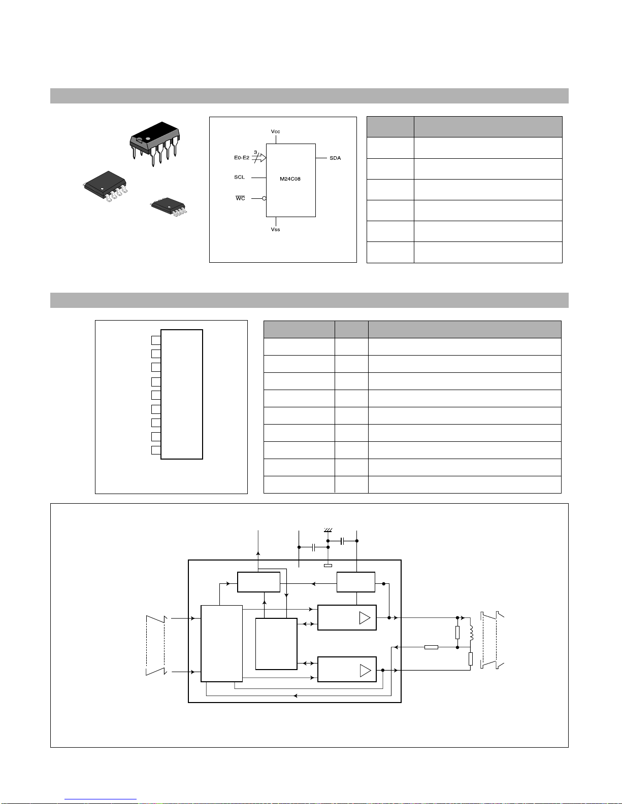
M24C08 Serial I2C BUS EEPROM
SYMBOL
E0-E2
SDA
SCL
WC
Vcc
Vss
DESCRIPTION
Chip Enable Input
Serial Data Address Input/Output
Serial Clock
Write Control
Supply Voltage
Ground
1
PSDIP8 (BN)
0.25mm Frame
8
1
1
SO8 (MN)
150mil Width
TSSOP8 (DW)
169mil Width
8
8
Logic Dirgram
TDA4867J PHILIPS 32P, SDIP
AMPLIFIER A
FLYBACK
GENERATOR
GUARD
CIRCUIT
INPUT STAGE
from e.g TDA485X
or SAA4856
INP
INN
IPROTECTION
AMPLIFIER B
4
9
6
8
1
2
357
OUTA
GUARO output/
power save mode
GND
FEEDB
OUTB
vertical
deflection
coil
R
p
V
p
V
FB
R
m
R
ref
I
defl
Block Diagram
SYMBOL
INP
INN
V
P
OUTB
GND
OUTA
V
FB
GUARD
FEEDB
DESCRIPTION
non-inverted input
inverted input
supply voltage
output B
ground
output A
flyback supply voltage
guard output
feedback inprt
PIN
1
2
3
4
5
6
7
8
9
INP
INN
V
P
OUTB
GND
OUTA
V
FB
GUARD
FEEDB
1
2
3
4
5
6
7
8
9
TDA4867J
Pin Configuration
Page 31
- 31 -
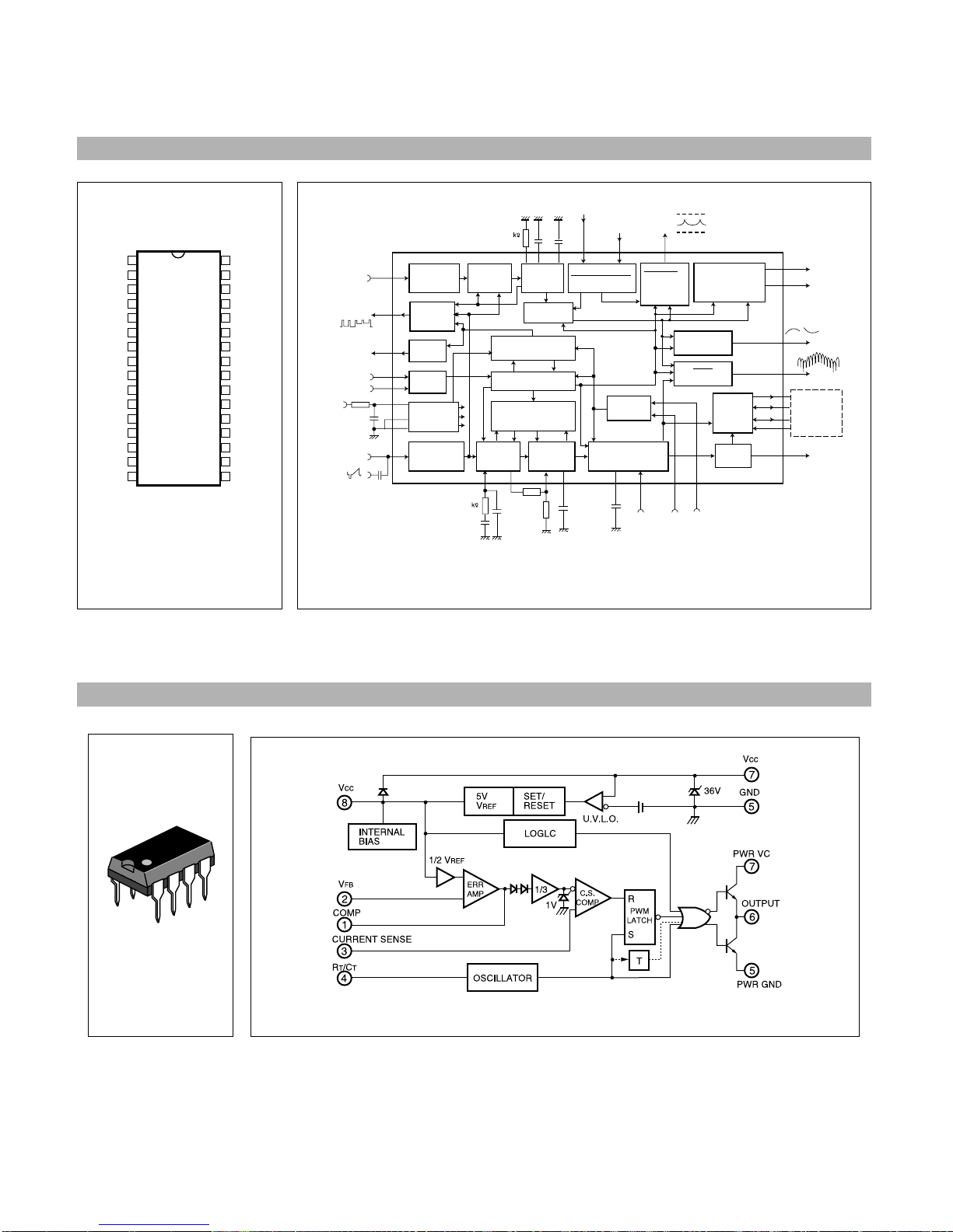
TDA4841PS PHLIPS 32P
1
2
3
4
5
6
7
8
9
10
11
12
13
14
15
16
32
31
30
29
28
27
26
25
24
23
22
21
20
19
18
17
FOCUS
HSMOD
HPLL2
HCAP
HREF
HBUF
HPLL1
SGND
VCAP
VREF
VAGC
VSMOD
ASCOR
SDA
SCL
HUNLOCK
HFLB
XRAY
BOP
BSENS
BIN
BDRV
PGND
HDRV
XSEL
Vcc
EWDRV
VOUT2
VOUT1
VSYNC
HSYBC
CLBL
TDA4841PS
Pin Configuration
V-sync
(TTL level)
(TTL level)
(video)
15
25
10
18
19
2
17
16
14
7
H/C-SYNC INPUT
AND POLARITY
CORRECTION
(1) See calculation of f range.
(2) See Figs 22 and 23.
SUPPLY
AND
REFERENCE
HUNLOCK
OUTPUT
VIDEO
CLAMPING
AND V-BLANK
V-SYNC INPUT
AND POLARITY
CORRECTION
V-SYNC
INTEGRATOR
VERTICAL
OSCILLATOR
AND AGC
EHT COMPENSATION
H-SIZE AND V-SIZE
EW-OUTPUT
V-OUTPUT
V-LINEARITY
V-LINEARITY BALANCE
H-PINCUSHION
H-CORNER
H-TRAPEZIUM
H-SIZE
OUTPUT
ASYMMETRIC
EW-CORRECTION
FOCUS
HORIZONTAL
AND VERTICAL
B+
CONTROL
B+ CONTROL
APPLICATION
H-OUTPUT
STAGE
X-RAY
PROTECTION
PLL2, PARALLELOGRAM,
PIN UNBALANCE AND
SOFT START
V-POSITION
V-SIZE, VOVSCN
TDA4841PS
I C-BUS
RECEIVER
2
I C-BUS REGISTERS
HUNLOCK
SDA
SCL
9.2 to 16V
H/C-sync
V+
clamping
blanking
PROTECTION
AND SOFT START
COINCIDENCE DETECTOR
FREQUENCY DETECTOR
PLL1 AND
H-POSITION
HORIZONTAL
OSCILLATOR
12
13
Vout2
Vout1
20 or
32
8
9
XSELX-RAYHFLB
213029
12
2%
1%
nF
10 nF
8.2
3.3
nF
100
nF
282726
(1)
R
HBUF
R
HREF
6
4
3
5
(2)
HDRV
23 24 22 21
VSMOD HSMOD
31 11
7V
1.2V
22
1%
5%
100 150
nF
nF
EHT compensaton
EHT compensation
via vertical size
via horizontal size
EWDRV
H
Block Diagram
KA3842B Current-Mode PWM Controller
1
8
BLOCK DIAGRAM
Page 32
- 32 -
- 33 -
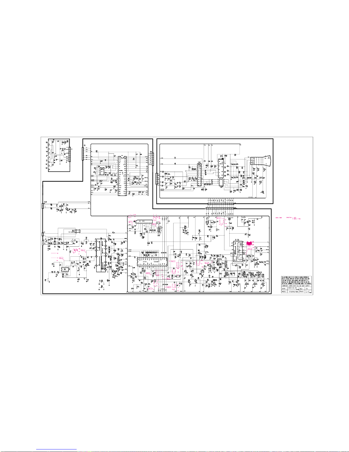
SCHEMATIC DIAGRAM
NOTICE
Since this is a basic schematic diagram.
The value of components and some partial connection are
sucject to be changed for improvement without notice.
Page 33
- 34 -
- 35-
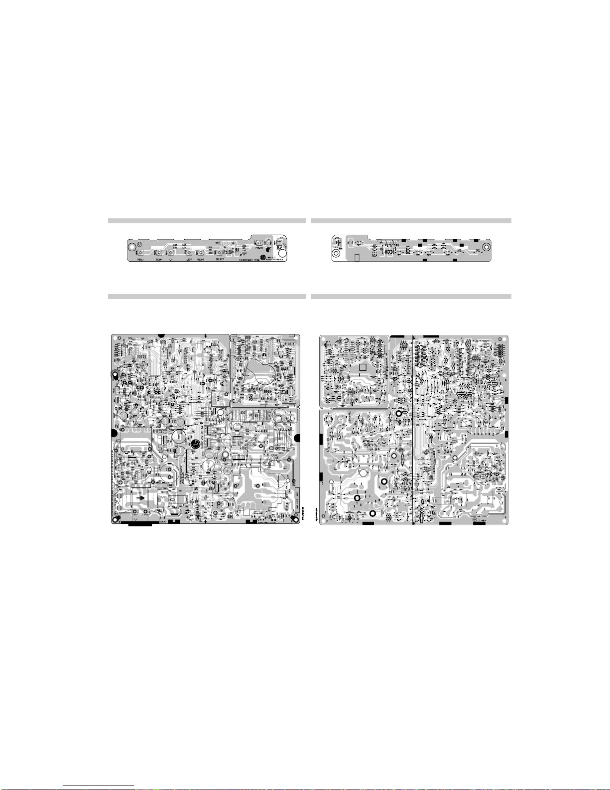
PRINTED CIRCUIT BOARD
1. CONTROL BOARD (Component Side)
2. CONTROL BOARD (Solder Side)
3. MAIN BOARD (Component Side)
4. MAIN BOARD (Solder Side)
Page 34

Jun. 2003
P/NO : 3828TSL091W Printed in Korea
 Loading...