

LG Flatron M3200C, Flatron M4200C-SAC, Flatron M4200C-BAC, Flatron M4200C-BAPC, Flatron M4200C-BATC Service Manual
...
COLOR MONIT OR
SER VICE MANUAL
Website:http://biz.LGservice.com
E-mail:http://www.LGEservice.com/techsup.html
CAUTION
BEFORE SERVICING THE UNIT,
READ THE SAFETY PRECAUTIONS IN THIS MANUAL.
CHASSIS NO. : CL-70
MODEL: M3200C (M3200C-SAFC.AL**LF)
M3200C (M3200C-BAFC.AL**LF)
M3200C (M3200C-BAC.AL**LF)
( ) **Same model for Service
1. LCD CHARACTERISTICS
Type : TFT Color LCD Module
Active Display Area : 31.51 inches(800.4mm) diagonal
Pixel Pitch : 170.25 (H) x 510.75 (V) x RGB
Color Depth : 8bits, 16,777,216 colors
Electrical Interface : LVDS
Size : 760(H) x 450(D) x 48(D)
Surface Treatment : Anti-Glare, Hard Coating(3H)
Operating Mode : Normally Black
Backlight Unit : 20EEFL (20lamps)
2. OPTICAL CHARACTERISTICS
2-1. Viewing Angle by Contrast Ratio ≥ 10
Left : -85° min., -88°(Typ) Right : +85° min., +88°(Typ)
Top : +85° min., +88°(Typ) Bottom : -85° min., -88°(Typ)
2-2. Luminance : 400(min), 500(Typ)
2-3. Contrast Ratio : 400(min), 600(Typ)
3. SIGNAL (Refer to the Timing Chart)
3-1. PC & Video Input
1)Signal Input : S-video,RCA, Component
2)Input Form : D-SUB Analog, DVI, V1(CVBS)
V2(SVHS), DVD(YCbCr),
HDTV(YPbPr), TV-NTSC(Opion)
3)Resolution(max) : Analog -1600 x 1200@60Hz
Digital -1280 x 1024@60Hz
3-2. Sync Input
Horizontal : 30 ~ 83kHz(Digital: 30~72kHz)
Vertical : 56 ~ 85Hz
Input Form : Separate, TTL,
Positive/Negative Digital
4. SPECIAL FUNCTION
4-1. Audio
1)Output Rating : 10W + 10W(Rated Output ± 10%)
2)Freq. Character : 100Hz~10KHz Range(-3dB)
3)T. H. D : Within 10%
4)Input Sensitivity : 0.700Vrms
4-2. Speaker
1)TYPE : Detachable
2)Impedance : 8Ϊ
3)Input : Max : 15W, Normal : 10W
4-2. AV
1)Video Level : Input : 0.7 ± 0.15Vp-p
2)Sync Level : Input : 0.286 ± 0.075Vp-p
3)Color Burst : Input : 0.214 ± 0.072Vp-p
4)Audio Level : NTSC Input : 0.40 ± 0.1Vrms
PAL Input : 0.5 ± 0.1Vrms
PC Input : 0.7 ± 0.1Vrms
5)Video Cross Talk : 43dB
5. POWER SUPPLY
5-1. Power Adaptor
Input : AC 100~240V, 50/60Hz , 2.8A
5-2. Power Consumption
6. ENVIRONMENT
6-1. Operating Temperature: 10°C~35°C
6-2. Operating Humidity : 10%~80%
6-3. MTBF : 50,000 HRS with 90%
Confidence level
Lamp Life : 50,000 Hours(Min.)
7. DIMENSIONS (with Speaker/Stand)
Width : 803 mm (31.61'')
Depth : 99.9 mm (3.93'')
Height : 493 mm (19.41'')
8. WEIGHT (with Speaker/Stand)
Net. Weight : 16 kg (35.28 lbs)
Gross Weight : 20.9 kg (46.08 lbs)
CONTENTS
SPECIFICATIONS
- 2 -
SPECIFICATIONS ................................................... 2
PRECAUTIONS ....................................................... 3
TIMING CHART ....................................................... 7
BLOCK DIAGRAM ................................................... 9
DESCRIPTION OF BLOCK DIAGRAM...................10
ADJUSTMENT ....................................................... 11
SERVICE OSD ...................................................... 13
TROUBLESHOOTING GUIDE .............................. 14
WIRING DIAGRAM ............................................... 20
EXPLODED VIEW...................................................21
REPLACEMENT PARTS LIST ...............................23
SCHEMATIC DIAGRAM......................................... 34
MODE
POWER ON (NORMAL)
STAND-BY
SUSPEND
DPM OFF
POWER OFF
H/V SYNC
ON/ON
OFF/ON
ON/OFF
OFF/OFF
-
POWER CONSUMPTION
less than 160 W
less than 4 W
less than 4 W
less than 4 W
less than 2 W
LED COLOR
GREEN
AMBER
AMBER
AMBER
OFF
VIDEO
ACTIVE
OFF
OFF
OFF
-
- 3 -
WARNING FOR THE SAFETY-RELATED COMPONENT.
• There are some special components used in LCD
monitor that are important for safety. These parts are
marked on the schematic diagram and the
replacement parts list. It is essential that these critical
parts should be replaced with the manufacturer’s
specified parts to prevent electric shock, fire or other
hazard.
• Do not modify original design without obtaining written
permission from manufacturer or you will void the
original parts and labor guarantee.
TAKE CARE DURING HANDLING THE LCD MODULE
WITH BACKLIGHT UNIT.
• Must mount the module using mounting holes arranged
in four corners.
• Do not press on the panel, edge of the frame strongly
or electric shock as this will result in damage to the
screen.
• Do not scratch or press on the panel with any sharp
objects, such as pencil or pen as this may result in
damage to the panel.
• Protect the module from the ESD as it may damage the
electronic circuit (C-MOS).
• Make certain that treatment person’s body are
grounded through wrist band.
• Do not leave the module in high temperature and in
areas of high humidity for a long time.
• The module not be exposed to the direct sunlight.
• Avoid contact with water as it may a short circuit within
the module.
• If the surface of panel become dirty, please wipe it off
with a softmaterial. (Cleaning with a dirty or rough cloth
may damage the panel.)
WARNING
BE CAREFUL ELECTRIC SHOCK !
• If you want to replace with the new backlight (CCFL) or
inverter circuit, must disconnect the AC adapter
because high voltage appears at inverter circuit about
650Vrms.
• Handle with care wires or connectors of the inverter
circuit. If the wires are pressed cause short and may
burn or take fire.
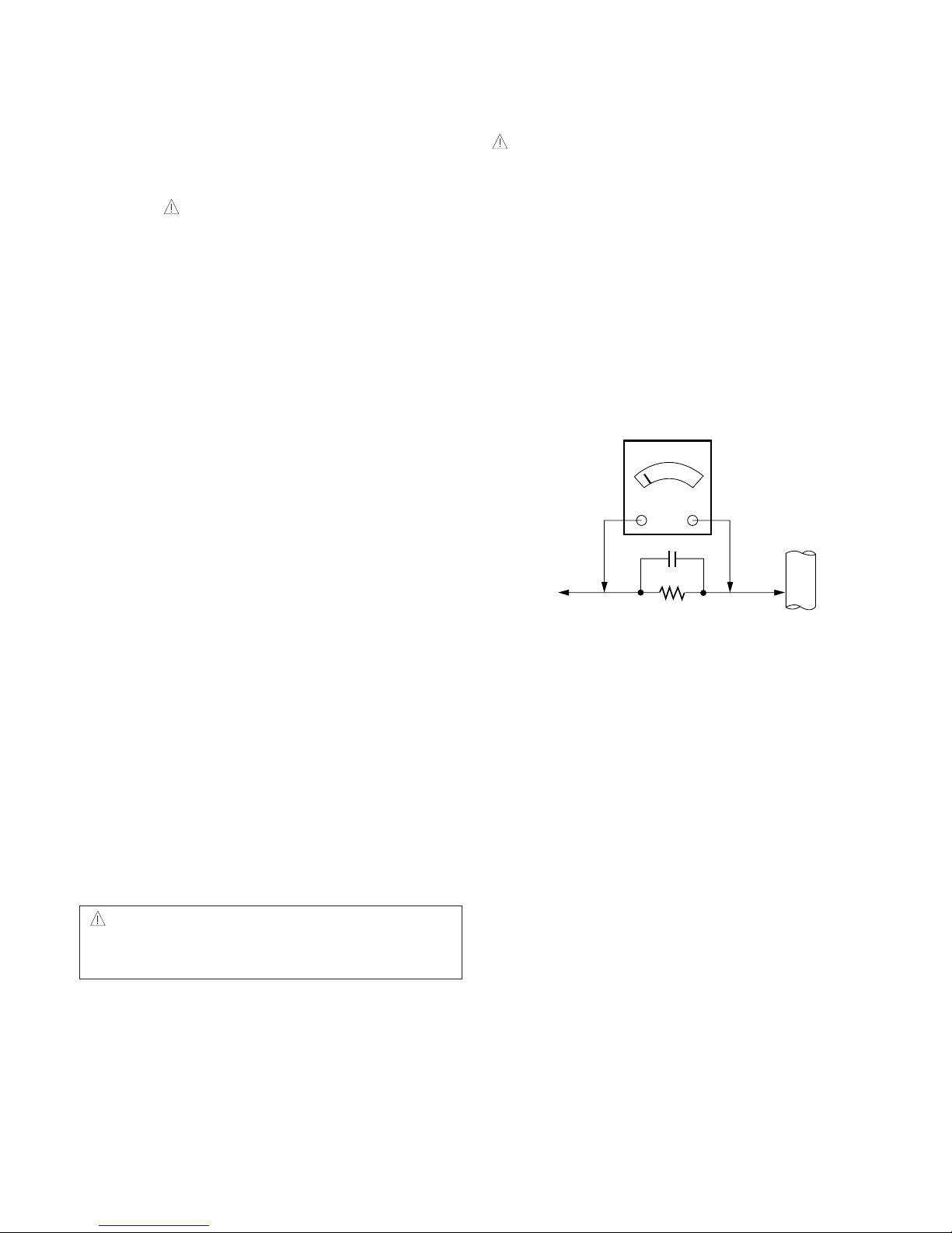
Leakage Current Hot Check Circuit
PRECAUTION
CAUTION
Please use only a plastic screwdriver to protect yourself
from shock hazard during service operation.
1.5 Kohm/10W
To Instrument's
exposed
METALLIC PARTS
Good Earth Ground
such as WATER PIPE,
CONDUIT etc.
AC Volt-meter

- 4 -
SERVICING PRECAUTIONS
CAUTION: Before servicing receivers covered by this
service manual and its supplements and addenda, read
and follow the SAFETY PRECAUTIONS on page 3 of this
publication.
NOTE: If unforeseen circumstances create conflict
between the following servicing precautions and any of the
safety precautions on page 3 of this publication, always
follow the safety precautions. Remember: Safety First.
General Servicing Precautions
1. Always unplug the receiver AC power cord from the AC
power source before;
a. Removing or reinstalling any component, circuit
board module or any other receiver assembly.
b. Disconnecting or reconnecting any receiver electrical
plug or other electrical connection.
c. Connecting a test substitute in parallel with an
electrolytic capacitor in the receiver.
CAUTION: A wrong part substitution or incorrect
polarity installation of electrolytic capacitors may
result in an explosion hazard.
d. Discharging the picture tube anode.
2. Test high voltage only by measuring it with an
appropriate high voltage meter or other voltage
measuring device (DVM, FETVOM, etc) equipped with
a suitable high voltage probe.
Do not test high voltage by "drawing an arc".
3. Discharge the picture tube anode only by (a) first
connecting one end of an insulated clip lead to the
degaussing or kine aquadag grounding system shield
at the point where the picture tube socket ground lead
is connected, and then (b) touch the other end of the
insulated clip lead to the picture tube anode button,
using an insulating handle to avoid personal contact
with high voltage.
4. Do not spray chemicals on or near this receiver or any
of its assemblies.
5. Unless specified otherwise in this service manual,
clean electrical contacts only by applying the following
mixture to the contacts with a pipe cleaner, cottontipped stick or comparable non-abrasive applicator;
10% (by volume) Acetone and 90% (by volume)
isopropyl alcohol (90%-99% strength)
CAUTION: This is a flammable mixture.
Unless specified otherwise in this service manual,
lubrication of contacts in not required.
6. Do not defeat any plug/socket B+ voltage interlocks
with which receivers covered by this service manual
might be equipped.
7. Do not apply AC power to this instrument and/or any of
its electrical assemblies unless all solid-state device
heat sinks are correctly installed.
8. Always connect the test receiver ground lead to the
receiver chassis ground before connecting the test
receiver positive lead.
Always remove the test receiver ground lead last.
9. Use with this receiver only the test fixtures specified in
this service manual.
CAUTION: Do not connect the test fixture ground strap
to any heat sink in this receiver.
Electrostatically Sensitive (ES) Devices
Some semiconductor (solid-state) devices can be
damaged easily by static electricity. Such components
commonly are called Electrostatically Sensitive (ES)
Devices. Examples of typical ES devices are integrated
circuits and some field-effect transistors and
semiconductor "chip" components. The following
techniques should be used to help reduce the incidence of
component damage caused by static by static electricity.
1. Immediately before handling any semiconductor
component or semiconductor-equipped assembly, drain
off any electrostatic charge on your body by touching a
known earth ground. Alternatively, obtain and wear a
commercially available discharging wrist strap device,
which should be removed to prevent potential shock
reasons prior to applying power to the unit under test.
2. After removing an electrical assembly equipped with
ES devices, place the assembly on a conductive
surface such as aluminum foil, to prevent electrostatic
charge buildup or exposure of the assembly.
3. Use only a grounded-tip soldering iron to solder or
unsolder ES devices.
4. Use only an anti-static type solder removal device.
Some solder removal devices not classified as "antistatic" can generate electrical charges sufficient to
damage ES devices.
5. Do not use freon-propelled chemicals. These can
generate electrical charges sufficient to damage ES
devices.
6. Do not remove a replacement ES device from its
protective package until immediately before you are
ready to install it. (Most replacement ES devices are
packaged with leads electrically shorted together by
conductive foam, aluminum foil or comparable
conductive material).
7. Immediately before removing the protective material
from the leads of a replacement ES device, touch the
protective material to the chassis or circuit assembly
into which the device will be installed.
CAUTION: Be sure no power is applied to the chassis
or circuit, and observe all other safety precautions.
8. Minimize bodily motions when handling unpackaged
replacement ES devices. (Otherwise harmless motion
such as the brushing together of your clothes fabric or
the lifting of your foot from a carpeted floor can
generate static electricity sufficient to damage an ES
device.)

- 5 -
General Soldering Guidelines
1. Use a grounded-tip, low-wattage soldering iron and
appropriate tip size and shape that will maintain tip
temperature within the range or 500。F to 600。F.
2. Use an appropriate gauge of RMA resin-core solder
composed of 60 parts tin/40 parts lead.
3. Keep the soldering iron tip clean and well tinned.
4. Thoroughly clean the surfaces to be soldered. Use a
mall wire-bristle (0.5 inch, or 1.25cm) brush with a
metal handle.
Do not use freon-propelled spray-on cleaners.
5. Use the following unsoldering technique
a. Allow the soldering iron tip to reach normal
temperature.
(500。F to 600。F)
b. Heat the component lead until the solder melts.
c. Quickly draw the melted solder with an anti-static,
suction-type solder removal device or with solder
braid.
CAUTION: Work quickly to avoid overheating the
circuitboard printed foil.
6. Use the following soldering technique.
a. Allow the soldering iron tip to reach a normal
temperature (500。F to 600。F)
b. First, hold the soldering iron tip and solder the strand
against the component lead until the solder melts.
c. Quickly move the soldering iron tip to the junction of
the component lead and the printed circuit foil, and
hold it there only until the solder flows onto and
around both the component lead and the foil.
CAUTION: Work quickly to avoid overheating the
circuit board printed foil.
d. Closely inspect the solder area and remove any
excess or splashed solder with a small wire-bristle
brush.
IC Remove/Replacement
Some chassis circuit boards have slotted holes (oblong)
through which the IC leads are inserted and then bent flat
against the circuit foil. When holes are the slotted type,
the following technique should be used to remove and
replace the IC. When working with boards using the
familiar round hole, use the standard technique as
outlined in paragraphs 5 and 6 above.
Removal
1. Desolder and straighten each IC lead in one operation
by gently prying up on the lead with the soldering iron
tip as the solder melts.
2. Draw away the melted solder with an anti-static
suction-type solder removal device (or with solder
braid) before removing the IC.
Replacement
1. Carefully insert the replacement IC in the circuit board.
2. Carefully bend each IC lead against the circuit foil pad
and solder it.
3. Clean the soldered areas with a small wire-bristle
brush. (It is not necessary to reapply acrylic coating to
the areas).
"Small-Signal" Discrete Transistor
Removal/Replacement
1. Remove the defective transistor by clipping its leads as
close as possible to the component body.
2. Bend into a "U" shape the end of each of three leads
remaining on the circuit board.
3. Bend into a "U" shape the replacement transistor leads.
4. Connect the replacement transistor leads to the
corresponding leads extending from the circuit board
and crimp the "U" with long nose pliers to insure metal
to metal contact then solder each connection.
Power Output, Transistor Device
Removal/Replacement
1. Heat and remove all solder from around the transistor
leads.
2. Remove the heat sink mounting screw (if so equipped).
3. Carefully remove the transistor from the heat sink of the
circuit board.
4. Insert new transistor in the circuit board.
5. Solder each transistor lead, and clip off excess lead.
6. Replace heat sink.
Diode Removal/Replacement
1. Remove defective diode by clipping its leads as close
as possible to diode body.
2. Bend the two remaining leads perpendicular y to the
circuit board.
3. Observing diode polarity, wrap each lead of the new
diode around the corresponding lead on the circuit
board.
4. Securely crimp each connection and solder it.
5. Inspect (on the circuit board copper side) the solder
joints of the two "original" leads. If they are not shiny,
reheat them and if necessary, apply additional solder.
Fuse and Conventional Resistor
Removal/Replacement
1. Clip each fuse or resistor lead at top of the circuit board
hollow stake.
2. Securely crimp the leads of replacement component
around notch at stake top.
3. Solder the connections.
CAUTION: Maintain original spacing between the
replaced component and adjacent components and the
circuit board to prevent excessive component
temperatures.

- 6 -
Circuit Board Foil Repair
Excessive heat applied to the copper foil of any printed
circuit board will weaken the adhesive that bonds the foil
to the circuit board causing the foil to separate from or
"lift-off" the board. The following guidelines and
procedures should be followed whenever this condition is
encountered.
At IC Connections
To repair a defective copper pattern at IC connections use
the following procedure to install a jumper wire on the
copper pattern side of the circuit board. (Use this
technique only on IC connections).
1. Carefully remove the damaged copper pattern with a
sharp knife. (Remove only as much copper as
absolutely necessary).
2. carefully scratch away the solder resist and acrylic
coating (if used) from the end of the remaining copper
pattern.
3. Bend a small "U" in one end of a small gauge jumper
wire and carefully crimp it around the IC pin. Solder the
IC connection.
4. Route the jumper wire along the path of the out-away
copper pattern and let it overlap the previously scraped
end of the good copper pattern. Solder the overlapped
area and clip off any excess jumper wire.
At Other Connections
Use the following technique to repair the defective copper
pattern at connections other than IC Pins. This technique
involves the installation of a jumper wire on the
component side of the circuit board.
1. Remove the defective copper pattern with a sharp
knife.
Remove at least 1/4 inch of copper, to ensure that a
hazardous condition will not exist if the jumper wire
opens.
2. Trace along the copper pattern from both sides of the
pattern break and locate the nearest component that is
directly connected to the affected copper pattern.
3. Connect insulated 20-gauge jumper wire from the lead
of the nearest component on one side of the pattern
break to the lead of the nearest component on the
other side.
Carefully crimp and solder the connections.
CAUTION: Be sure the insulated jumper wire is
dressed so the it does not touch components or sharp
edges.
TIMING CHART
- 7 -
VIDEO
SYNC
B
D
C
F
E
A
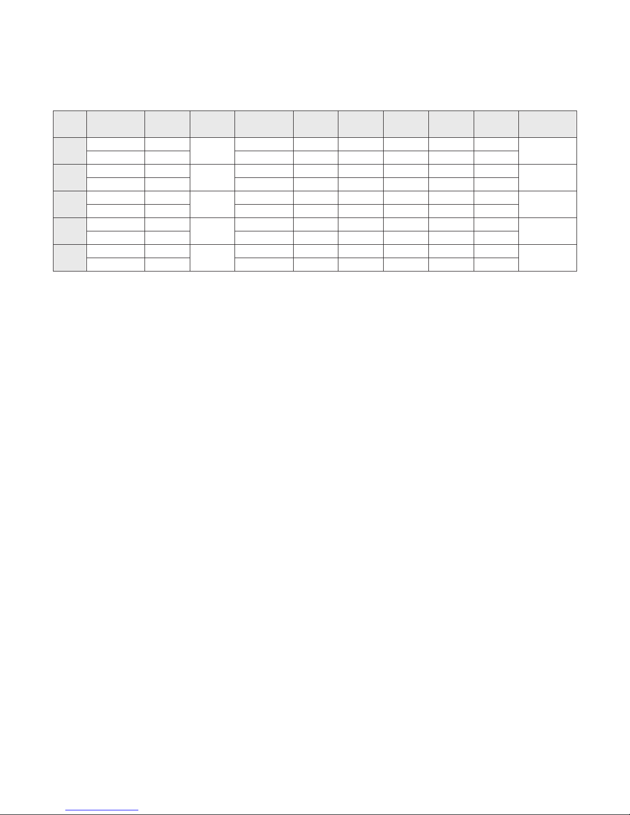
<< Dot Clock (MHz), Horizontal Frequency (kHz), Vertical Frequency (Hz), Horizontal etc... (µs), Vertical etc... (ms) >>
1) PC Mode
※1~17 : D-SUB, DVI-D: 1~15
MODE
H / V
Sync
Polarity
Frequency
Total
Period
( E )
Video
Active
Time ( A )
Front
Porch
( C )
Sync
Duration
( D )
Back
Porch
( F )
Resolution
Dot
Clock
1 H(Pixels) + 25.175 31.469 800 640 16 96 48 640 x 350
V(Lines) - 70.8 449 350 37 2 60
2 H(Pixels) - 28.321 31.468 900 720 18 108 54 720 X 400
V(Lines) + 70.8 449 400 12 2 35
3 H(Pixels) - 25.175 31.469 800 640 16 96 48 640 x 480
V(Lines) - 59.94 525 480 10 2 33
4 H(Pixels) - 31.5 37.5 840 640 16 64 120 640 x 480
V(Lines) - 75 500 480 1 3 16
5 H(Pixels) - 36.0 43.269 832 640 56 56 80 640 x 480
V(Lines) - 85.0 509 480 1 3 25
6 H(Pixels) + 40.0 37.879 1056 800 40 128 88 800 x 600
V(Lines) + 60.317 628 600 1 4 23
7 H(Pixels) + 49.5 46.875 1056 800 16 80 160 800 x 600
V(Lines) + 75.0 625 600 1 3 21
8 H(Pixels) + 56.25 53.674 1048 800 32 64 152 800 x 600
V(Lines) + 85.061 631 600 1 3 27
9 H(Pixels) +/- 57.283 49.725 1152 832 32 64 224 832 x 624
V(Lines) +/- 74.55 667 624 1 3 39
10 H(Pixels) - 65.0 48.363 1344 1024 24 136 160 1024 x 768
V(Lines) - 60.0 806 768 3 6 29
11 H(Pixels) - 78.75 60.123 1312 1024 16 96 176 1024 x 768
V(Lines) - 75.029 800 768 1 3 28
12 H(Pixels) + 94.5 68.68 1376 1024 48 96 208 1024 x 768
V(Lines) + 85.00 808 768 1 3 36
13 H(Pixels) + 74.5 44.772 1664 1280 64 128 192 1280 x 720
V(Lines) + 59.855 748 720 3 5 20
14 H(Pixels) + 84.75 47.72 1776 1360 72 136 208 1360 x 768
V(Lines) + 59.799 798 768 3 5 22
15 H(Pixels) + 108.0 63.981 1688 1280 48 112 248 1280 x 1024
V(Lines) + 60.02 1066 1024 1 3 38
16 H(Pixels) + 135.00 79.98 1688 1280 16 144 248 1280 x 1024
V(Lines) + 75.02 1066 1024 1 3 38
17 H(Pixels) + 162.00 75.00 2160 1600 90 30 88 1600 x 1200
V(Lines) + 60 1250 1200 1 3 46
- 8 -
2) Component Video Mode(Y/Pb/Pr)
MODE
H / V
Sync
Polarity
Frequency
Total
Period
( E )
Video
Active
Time ( A )
Front
Porch
( C )
Sync
Duration
( D )
Back
Porch
( F )
Resolution
Dot
Clock
1 H(Pixels) - 25.175 31.469 800 640 16 96 48 SDTV
V(Lines) - 59.94 525 480 10 2 33 480
2 H(Pixels) - 27.027 31.5 858 720 16 62 60 HDTV
V(Lines) - 60 525 480 10 2 33 720P (HDCP)
3 H(Pixels) - 74.176 44.955 1650 1280 70 40 260 HDTV
V(Lines) - 59.94 750 720 5 5 60 720P (HDCP)
4 H(Pixels) - 74.250 33.750 2200 1920 44 44 192 HDTV
V(Lines) - 60.053 562 540 2 5 15 1080I (HDCP)
5 H(Pixels) - 74.176 33.716 2200 1920 44 44 192 HDTV
V(Lines) - 59.994 562 540 2 5 15 1080I (HDCP)
- 9 -
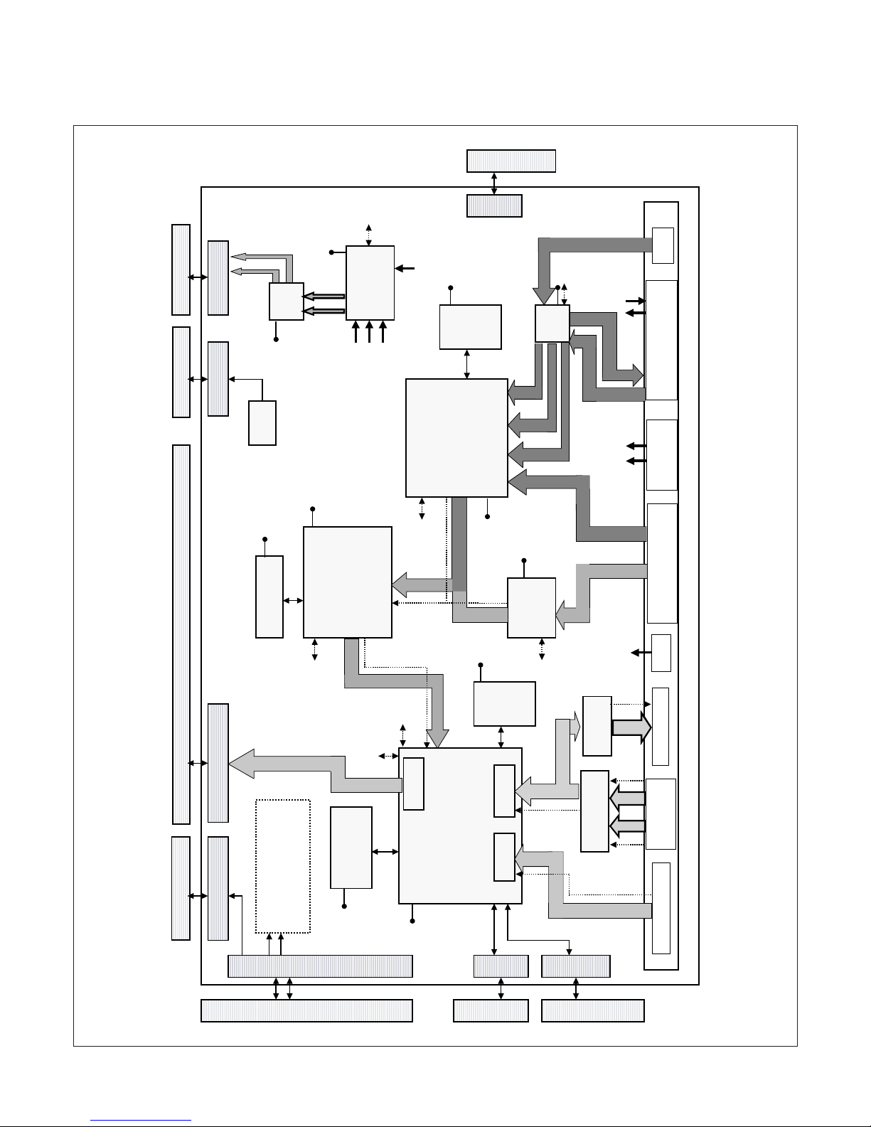
DVI
RGB1
RGB2
RGB Out
PC
Sound
Component1 In
Component2 In
Component1(2)
Sound
CVBS In
CVBS Out
S-VIDEO
LCD Module
Inverter Assy
Power Assy
RS232 In/Out
Video Signal P rocessor
(U402)
ADC
TMDS
LVD S
128Mb DDR
FRC Memory
(U401)
8Mb
Flash
Memory
(U403)
r
(480
i ~ 1080i)
(480i/576i)
Comp1
Comp2
S/W
(U201)
(CXA2040AQ)
Y/C
ADC
(U303)
(MST9883C)
4:2:2 (16bit)
Video Decoder
(U801)
(UPD64012)
SDRAM
(U802)
(K4S161622)
De-interlace
(U901)
(MDIN150L)
(K4S643232)
SDRAM (U902)
(M29W800DT)
Audio
Decoder
(U501)
(MSP3420G)
Amp
(U502)
(TPA3004)
(gm1501H-CF-LF)
(HY5DU283222AQ)
Signal Selector
(U121)
RGB
(SOG)
RGB
(SOG)
Low
Distortion
Amp
RGB
(SOG)
TMDS
LVD S
12P Wafer 30P Wafer
Regulator
Power FET Block
4:2:2 (16
bit)
HD-YPbP
CVBS OUT
Y OUT
C OUT
CVBS OUT
CVBS IN
4:2:2
(16bit)
YCbCr
Control Assy
15P W afer
10P W afer 9P Wafer
1.5V/1.8V/2.5V/3.3V/5V/
12V/18V
24V
12P W afer
FAN Assy (42 ”)
Temp
Sensor
(LM35DT)
(U523)
Speaker Assy
4P Wafer
5P Wafer
Logo LED Assy
Left Right
RightLeft
PC Audio
Component
Audio
CVBS
Audio
DTV Audio (Comp1)
DVD Audio (Comp2)
PC Audio
CVBS Audio
SCL
SDA
H/V
SCL
SDA
H/V
SCL
SDA
H/V
SCL
SDA
H/V
SCL
SDA
SCL2/SDA2
SCL/SDA
SCL/SDA
H/V/CLK
H/V/CLK
4:2:2
(16bit)
SCL2/SDA2
SCL/SDA
SCL2/SDA2
SCL/SDA
5V/8V
18V
1.8V
2.5V
3.3V
2.5V
3.3V
1.5V/3.3V
3.3V
2.5V/3.3V
3.3V
(BA7657F)
9V
3.3V
(AD8009)
BLOCK DIAGRAM(uPD64011+gm1501H)

- 10 -
DESCRIPTION OF BLOCK DIAGRAM
1. INPUT SELECTION CIRCUIT
1) D-SUB RGB INPUT SELECT : This section is
composed of Signal selector IC(BA7657F_U121)
and peripheral devices.
The BA7657F(U121) IC select RGB1 signal or
RGB2 signal and the signal is sent to gm1501H
(U402).
2) VIDEO INPUT SELECT : This section is composed
of Video switching IC (CXA2040AQ_U201) and
peripheral devices.
Video switching IC(CXA2040AQ_U201) select
CVBS video or S-video and the signal is sent to
Video decoder (UPD64012)
3) DVI signal input is directly fed to SCALER,
DTV(Component1) signal input is given to Scaler
IC(U402) via MST9883C(U303) DVD(Component2)
signal input is given to Scaler IC via Video Decoder
IC(UPD64012_U801).
2. DDC COTROLLER
This section is composed gm1501H(U402),EEPROM
IC (U404, U115, U120) and peripheral devices.
gm1501H(U402) is controlling peripheral devices
through IIC Line.
Major functions of this block are :
(1) Controlling of u-COM and Flash memory through
DDC-SCLA, DDC-SDAA of D-sub connector.
(2) Storage of EDID DATA in the EEPROM(U115,
U120).
3. ANALOG DIGITAL CONVERTER
This section is composed of MST9883C(U303) and
peripheral devices.
gm1501H(U402) is controlling MST9883C through IIC
Line.
This IC is converting DTV(YPbPr) signal in to 16 bit
Interlace signal and the signal is sent to De-interlace
IC(MDIN150L_U901)
This output signal have CONTRAST, BRIHTNESS,
SHARPNESS, COLOR, TINT information.
3. VIDEO DECODER
This section is composed of UPD64012(U801) and
peripheral devices.
gm1501H(U402) is controlling UPD64012 through
IIC Line.
This IC is controlling CVBS input signal ,S-VIDEO(Y/C)
input signal and DVD(YCbCr) input signal and
converting input signals in to 16 bit interlace signal and
the signal is sent to De-interlace IC(U901).
This output signal have CONTRAST, BRIHTNESS,
SHARPNESS, COLOR, TINT information.
4. DE-INTERLACER
This section is composed of MDIN150L(U901) and
peripheral devices.
gm1501H(U402) is controlling MDIN150L through IIC
Line.
This IC is converting 16bit interlace input signal in to
16bit De-interlace signal and the signal is sent to
Video Signal Processor IC(gm1501H_U402).Ä
5. AUDIO DECODER
This section is composed of MSP3420G(U501) and
peripheral devices.
gm1501H(U402) is controlling MSP3420G through IIC
Line.
This IC is processing audio signal output of A/V Jack,
PC Audio Jack.
This IC's output signal is sent to Audio Amplifier
IC(TPA3004_U502).
6. AUDIO AMPLIFIER
This section is composed of TPA3004(U502) OR
TPA3001(U507) and peripheral devices.
Audio Amplifier's function is amplification of sound
signal received from Audio Decoder.
Input Audio signal is amplified according to the DC
Volume control curve.
7.
VIDEO SIGNAL PROCESSOR (FORMAT CONVERTER)
This section is composed of gm1501H(U402) and
peripheral devices.
gm1501H(SCALER_U402) have in built u-COM in IC.
(1) This IC include A/D Converter, Pre-Amp, PLL
Circuit.
(2) This IC include TMDS Receiver and LVDS
Transmitter.
TMDS Receiver is decoding input DVI Signal and
LVDS Transmitter is encoding the output Signal .
also, gm1501H have Format Converter (Scaling)
function.
This IC convert Various sized Digital signal to LCD
Module's resolution (WXGA).
8. DC/DC COVERTER
DC/DC Converters change Power output voltage (DC
5V, 12V, 24V) to 1.5V, 2.5V, 3.3V, 5V, 8V, 9V.
(To be used by different IC on the main board.)
9. TEMPERATURE SENSING AND FAN CONTROL
This section is composed of LM35DT(U523),
KIA358F(U524) and peripheral devices.
The temperature at surface of LM35DT(U523) is
sensed and converted to HEX code by KIA358(U524).
gm1501H(U402) receives sensing HEX values from
KIA358F(U524)and control FAN(42INCH ONLY).
10. POWER SUPPLY BLOCK
Power supply receives AC voltage (100-240 V, 50/60
Hz,) and converts to System voltage that are 5V, 12V,
18V and 24V DC voltage.
These voltages supports main board, inverter board
and module;s T-con board.
This Circuit contains PFC(Power Factor Correction)
circuit.
The Minimum Power efficiency is about 75%.
- 11 -
ADJUSTMENT
All adjustment are thoroughly checked and corrected
when the monitor leaves the factory, but sometimes
several minor adjustment may be required.
Adjustment should be following procedure and after
warming up for a minimum of 30 minutes.
• Alignment appliances and tools.
- IBM compatible PC
- Programmable Signal Generator.
(eg. VG-819 made by Astrodesign Co.)
- Oscilloscope.
- White Balance Meter. (CA-110)
1. DDC Data Write Procedure-Analog
1) Use this procedure only when there is some
problem on Analog EDID data.
2) Run alignment program for M3200C on the IBM
compatible PC.
3) Select EEPROM → Analog EDID write command
and Enter.
4) This will write the Analog EDID data to EEPROM.
2. DDC Data Write Procedure-Digital
1) Use this procedure only when there is some
problem on Digital EDID data.
2) Run alignment program for M3200C on the IBM
compatible PC.
3) Select EEPROM → Digital EDID write command
and Enter.
4) This will write the Digital EDID data to EEPROM.
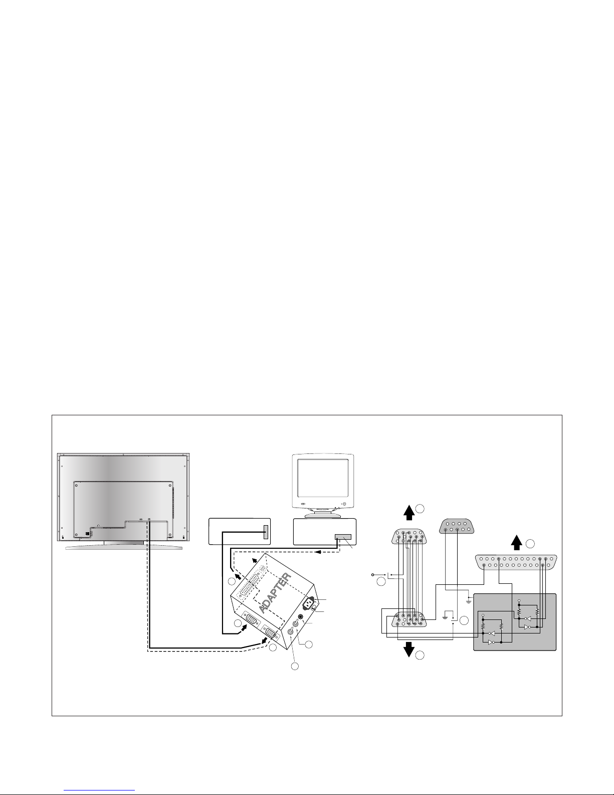
RS-232C
EXT.
220
IBM
Compatible PC
Parallel Port
Power inlet (required)
Power LED
ST Switch
Power Select Switch
(110V/220V)
Control Line
Not used
RS232C
PARALLEL
V-SYNC
POWER
ST
VGS
MONITOR
E
V-Sync On/Off Switch
(Switch must be ON.)
F
A
B
C
5V
E
F
A
B
C
15
10
5
5
69
1
1
1
14
13
25
6
5V
5V
4.7K
4.7K
4.7K
74LS06
74LS06
OFF ON
OFF
ON
11
Figure 1. Cable Connection
- 12 -
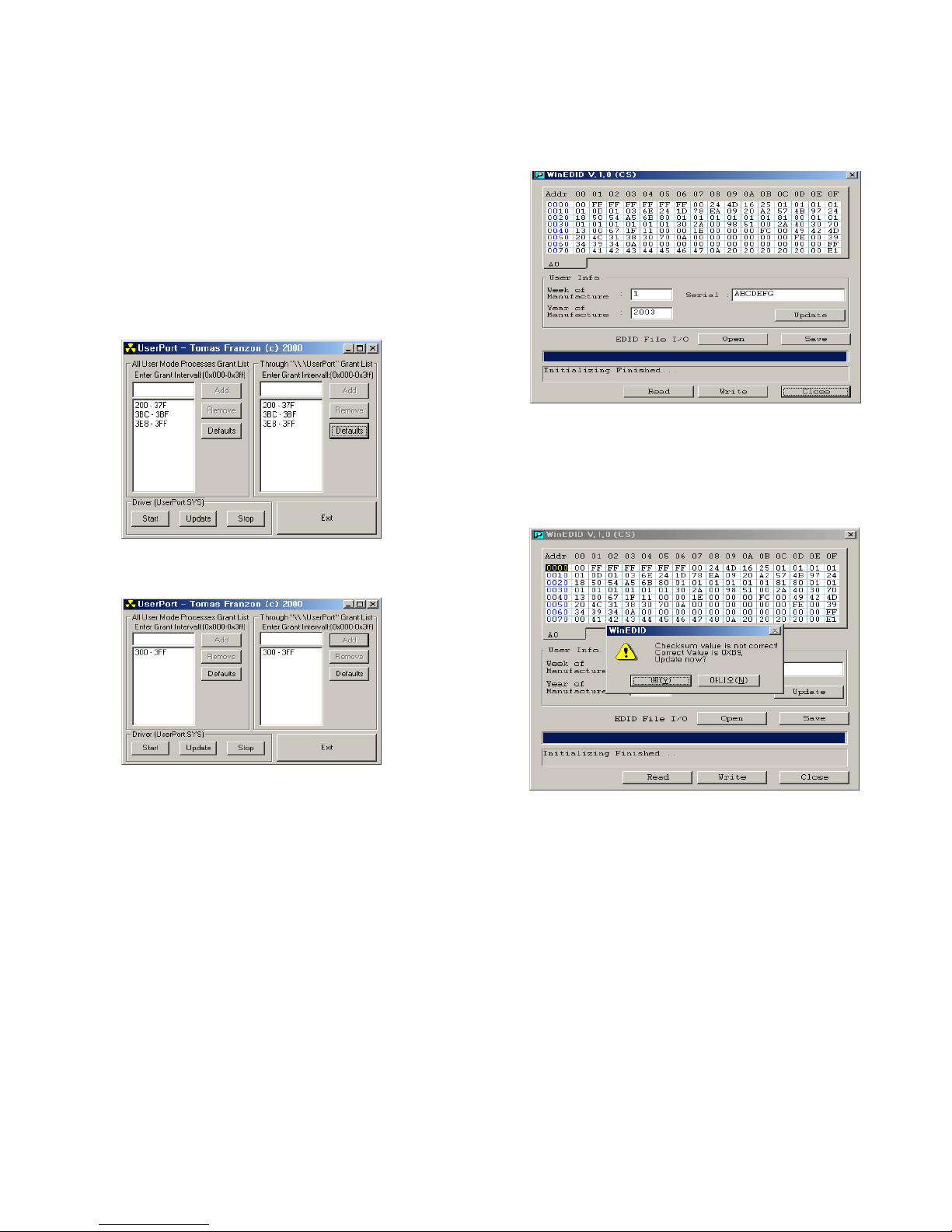
Windows EDID V1.0 User Manual
Operating System: MS Windows 98, 2000, XP
Port Setup: Windows 98 => Don’t need setup
Windows 2000, XP => Need to Port Setup.
This program is available to LCD Monitor only.
1. Port Setup
a) Copy “UserPort.sys” file to
“c:\WINNT\system32\drivers” folder
b) Run Userport.exe
c) Remove all default number
d) Add 300-3FF
e) Click Start button.
f) Click Exit button.
2. EDID Read & Write
1) Run WinEDID.exe
2) Edit Week of Manufacture, Year of Manufacture,
Serial Number
a) Input User Info Data
b) Click “Update” button
c) Click “ Write” button
- 13 -
SERVICE OSD
SEREVICE MENU
Model :
Elapsed Time 17H
V1.0M3200C
NVram Inatial OFF
RS232 Speed 115.2K
WB Adjust 0
Aging Mode OFF
Model Select M3200C
TV <-> AV AV
Contry Option USA
SEREVICE MENU
Model :
Resolution Auto
Elapsed Time 17H
AI OFF
Hotel Mode SET
SVC Display SET
Video H Position 50
Video V Position 50
Normal
RS232 Select
LG Hotel Mode Set Up
Channel Change YES
Channel Menu Display YES
Input Mode Change YES
100
30
Volume Limit
Fixed V olume YES
OSD Display YES
Remocon Operation YES
Local Key Operation YES
On Monitor Operation
Volume On
1
Channel On
YES
Auto Off Operation YES
■ Engaging the `in-start' key of the remote control lets you
into the Service Menu
■ Description of operation
- Elapsed time : Time used for back light
- Nvram Initial : EEPROM reset
- RS232 Speed : Baud Speed
- WB Adjust : Adjusts the white balance
- Aging Mode : Sets the aging mode
- Model Select : Sets the model name
- TV <-> AV : Sets the TV or AV only Model
- Country Option : Chooses a country
■ Caution
- To use the functions of the existing Special Menu, use Power Off/On.
■ Description of operation
- Resolution : Adjusts the picture resolution
- AI : Function built in panel
- Hotel Mode : Function for a Hotel system manager
- SVC Display : Adjusts the service screen quality
- Video H Position : Adjusts Video H position
- Video V Position : Adjusts Video V position
- RS232 Select : Adjusts RS232 comunication type.
■ The OSD is displayed when Audio Key is pressed on Nvram
Initial in Service Menu.
■ Purpose
- Function :
The setting can be adjusted when the unit is being used in a hotel.
■ Description of operation
- Channel Change :
Enables (Yes)/Disables (No) channel change in the TV source mode.
- Input Source Change : Enables (Yes)/Disables (No) input source change.
- Volume Limit : Sets the maximum volume within the range of 0 ~ 100 when
volume control is allowed.
- Fixed Volume : Sets Yes (Fixed)/No (Variable) about whether the sound
volume will be fixed to the current value or not.
- OSD Display : Sets whether the OSD will be displayed (Yes) or not (No).
- Remote Control Operation : Activates (Yes)/Deactivates (No) remote
control operation.
- Local Key Operation : Activates (Yes)/Deactivates (No) local key operation.
- On Monitor Operation : Sets Yes (Operation)/No (No operation) about
whether the channel and the volume level that will be displayed when the
power is turned on.
- Channel : Sets Yes (Operation)/No (No operation) about whether the preset
channel will be selected or the one memorized last will be selected when the
power is turned on. On (Activated) or Off (Deactivated) can be selected.
- Channel Menu Display: Enables (Yes)/Disables (No) entry into the Channel
menu on the main OSD.
- Auto Off Operation : Sets whether the automatic turn-off function will be
activated or not with On (Activated) or Off (Deactivated) option, which turns
off the TV if no key input is made for 2 hours, using Auto Off operation and
On Time on the Time menu.
- 14 -
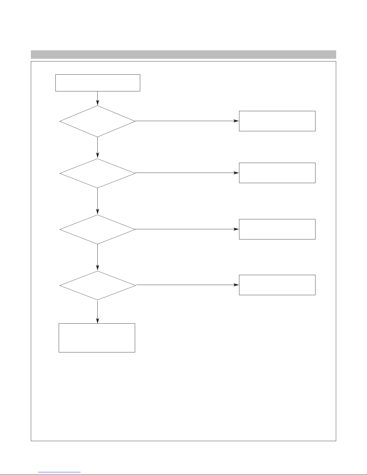
TROUBLESHOOTING GUIDE
1. NO POWER
NO POWER
(POWER INDICATOR OFF)
CHECK POWER BOARD
CHECK J601 VOLTAGE
(18V, 12V, 5V)?
NO
CHECK POWER BOARD
CHECK
J603 VOLTAGE
(12V, 24V) ?
NO
1. KEY PART IC CHECK
(U401, U402,U403)
2. CHECK KEY CONTROL
BOARD
YES
YES
YES
YES
CHECK X401
CHECK
X401
(14.318MHz) ?
NO
CHECK MICOM(U402)
SUB POWER PORT
CHECK J601
(SUB POWER) ?
NO
 Loading...