

LG FLATRON M228WA Series, M228WA-BZH.AQLP, M198WA-BZH.AQLP, M208WA-BZH.AQLP Service Manual
COLOR MONITOR
SERVICE MANUAL
Website:http://biz.LGservice.com
E-mail:http://www.LGEservice.com/techsup.html
CAUTION
BEFORE SERVICING THE UNIT,
READ THE SAFETY PRECAUTIONS IN THIS MANUAL.
CHASSIS NO. : LP69G
MODEL: M228WA (M228WA-BZH.A**QLP)
*( ) **Same model for Service
- 2 -
CONTENTS
SPECIFICATIONS ................................................... 2
PRECAUTIONS ....................................................... 8
DISASSEMBLY .......................................................12
BLOCK DIAGRAM ................................................. 14
DESCRIPTION OF BLOCK DIAGRAM...................15
ADJUSTMENT ...................................................... 17
TROUBLESHOOTING GUIDE .............................. 24
EXPLODED VIEW...................................................30
REPLACEMENT PARTS LIST ...............................32
SCHEMATIC DIAGRAM..........................................40
1. Application range
This specification is applied to 22" Wide Monitor TV used
LP69G chassis.
2. Requirement for Test
Each part is tested as below without special appointment.
(1) Power Voltage : Standard input voltage (100~240V@,
50/60Hz)
*Standard Voltage of each products is marked by models.
(2) Specification and performance of each parts are followed
each drawing and specification by part number in
accordance with BOM.
(3) The receiver must be operated for about 20 minutes prior
to the adjustment.
3. Test method
3.1 Performance : LGE test method followed
3.2 Demanded other specification
Safety : CE, IEC Specification
EMC : CE, IEC
SPECIFICATION
NOTE : Specifications and others are subject to change without notice for improvement
.
4-1. General Specification
4.1.1 TV
4. General Specification(TV)
No Item Specification Remark
1 Video input applicable system PAL-D/K, B/G, I, SECAM L, NTSC, NTSC 4.43
2 Receivable Broadcasting System PAL/SECAM BG (BZH/BTH)
PAL/SECAM DK EU/Non-EU
PAL I (PAL Market)
SECAM L/L’
3 RF Input Channel VHF : E2 ~ E12
UHF : E21 ~ E69 PAL
CATV : S1 ~ S20
HYPER : S21~ S41
L/L’ : B, C, D FRANCE
4 Input Voltage 100-240V~, 50Hz/60Hz
5 Market EU
6 Tuning System FVS 100 program PAL, 200 PR.(Option)
FS NTSC
7 Operating Environment Temp : 10°C~ 35°C
Humidity : 20% ~ 80%
8 Storage Environment Temp : -10°C ~ 60°C non condensing
Humidity : 5%~90% non condensing
9 Display LCD Module
- 3 -
No. Item Min Typ. Max Unit Remark
1. Type TFT Color LCD Module
2. Active Display area 473.76 (H) x 296.1 (V) mm
3. Outline dimension 493.7 (H) x 320.1 (V) x16.5 (D) mm Typ
4. Pixel pitch 0.282mm (H) x 0.282mm (V) x RGB mm
5. Color arrangement RGB vertical stripe
6. Color Depth 16.7M color
7. Electrical Interface LVDS
8. Surface Treatment Hard coating(3H) & Anti-glare(Haze 25)
9. Operating Mode Normally White
10. Back light Unit 4 CCFL (4 lamps)
11. R/T R.T : 2ms + R.T : 3ms Typ.
No. Item Specification Remark
1 Supported Sync. Type Separate Sync., Digital
2 Operating Frequency Analog Horizontal 28 ~ 83kHz
Vertical 56 ~ 75 Hz
Digital Horizontal 28 ~ 83kHz
Vertical 56 ~ 75 Hz
3 Resolution Analog Max. 1680 x 1050 @ 60Hz
Recommend 1680 x 1050 @ 60Hz
Digital Max. 1680 x 1050 @ 60Hz
Recommend 1680 x 1050 @ 60Hz
4 Input Voltage Voltage :100 - 240 Vac, 50 or 60Hz
5 Inrush Current Cold Start : 50 A Hot : 120 A
6 Operating Condition Sync (H/V) Video LED Wattage
Power S/W On
On mode
On/On Active Blue 60W Max.
On/On Active Blue 50W Typ.
Sleep mode
Off/On
Off Amber 1W
On/Off
Power S/W Off Off mode - Off Off 1W
7 MTBF 50,000 HRS with 90% Confidence level Lamp Life : 50,000 Hours(min)
8 Using Altitude 5,000 m (for Reliability) 3,000m(for FOS)
9 Operating Environment Temp : 10°C ~ 35°C
Humidity : 20% ~ 80%
10 Storage Environment Temp : -10°C ~ 60°C non condensing
Humidity : 5% ~ 90% non condensing
4.1.2 RGB/DVI
4-2. Module Specification(CMO M220Z1-L01, P/N:EAJ33527501_ZBD, EAJ33527502_Non-ZBD)
- 4 -
4-3. Optical characteristic specifications
4.3.1 Optical Characteristic
No. Item Specification Remark
Min Typ Max
1 Viewing Angle R/L 75/75 85/85
<CR≥10> U/D 70/70 80/80
2 Luminance Luminance RGB-PC 250 300 PSM:Dynamic, CSM: 6500K
(cd/m2) AV1/AV2/TV
190 230 PSM:Dynamic, CSM:Cool
Component
White Luminance Uniformity
1.3 1.5
3 Contrast Ratio CR RGB-PC/
At DFC Mode
AV1/AV2/TV/ 450 700
Typ. 3000:1, Min. 2400:1
Component
4 CIE Color Coordinates WHITE Wx 0.313
Wy 0.329 In RGB-PC input
RED Rx 0.644
Ry 0.333 PSM : Dynamic
GREEN Gx 0.286 CSM : 6500K
Gy 0.605 White
BLUE Bx 0.152 (100 IRE)
By 0.076
WHITE Wx 0.285
Wy 0.293 In AV1/AV2/Component/TV input
RED Rx 0.640
Ry 0.334 PSM : Dynamic
GREEN Gx 0.286 CSM : Cool
Gy 0.599 White
BLUE Bx 0.154 (85 IRE)
By 0.077
Typ.
+0.03
Typ.
+0.015
Typ.
-0.03
Typ.
-0.015
- 5 -
5. Component Video Input (Y, PB, PR)
No Resolution H-freq(kHz) V-freq.(kHz) Pixel clock(MHz) Proposed
1. 720*480 15.73 59.94 13.500 480i
2. 720*480 15.75 60.00 13.514 480i
3. 720*576 15.625 50.00 13.500 576i
4. 720*480 31.47 59.94 27.000 480p
5. 720*480 31.50 60.00 27.027 480p
6. 720*576 31.25 50.00 27.000 576p
7. 1280*720 44.96 59.94 74.176 720p
8. 1280*720 45.00 60.00 74.250 720p
9. 1280*720 37.50 50.00 74.25 720p
10. 1920*1080 33.72 59.94 74.176 1080i
11. 1920*1080 33.75 60.00 74.250 1080i
12 1920*1080 28.125 50.00 74.250 1080i
4-4. Model Specification
No Item Specification Remark
1. Market EU
2. Broadcasting system PAL BG/I/DK, SECAM-L/L’,
SECAM BG/DK
3 RF Input Channel VHF : E2 ~ E12
UHF : E21 ~ E69 PAL
CATV : S1 ~ S20
HYPER : S21~ S41
L/L’ : B, C, D FRANCE
4. SCART Input (1EA) PAL, SECAM
5. CVBS Input (1EA) PAL, SECAM, NTSC 4 System(Rear) :PAL50, SECAM,
NTSC, PAL60
6. S-Video Input (1EA) PAL, SECAM, NTSC 4 System(Rear) : PAL50, SECAM,
NTSC, PAL60
7. Component Input (1EA) Y/ Pb/Pr 480i/480p/576i/576p/720p/1080i
8. RGB Input (1EA) RGB-PC Max 1680 * 1050@60Hz
RGB-DTV 480p, 576p, 720p, 1080i
9. DVI Input (1EA) DVI-PC Max 1680 * 1050@60Hz
DVI-DTV 480p, 576p, 720p, 1080i
10. Audio Input (3 EA) CVBS, PC Audio, Component L/R Input
- 6 -
6. RGB Input (PC)
No Resolution H-freq(kHz) V-freq.(Hz) Pixel clock(MHz)
1 720*400 31.468 70.08 28.321
2 640*480 31.469 59.94 25.175
3 640*480 37.5 75 31.5
4 800*600 37.879 60.317 40.0
5 800*600 46.875 75.0 49.5
6 1024*768 48.363 60.0 65.0
7 1024*768 60.123 75.029 78.75
8 1152*864 67.500 75.000 108.0
9 1280*1024 63.981 60.02 108.0
10 1280*1024 79.976 75.035 135.0
11 1680*1050 64.674 59.883 119.0
12 1680*1050 65.290 59.954 146.25
No Resolution H-freq(kHz) V-freq.(kHz) Pixel clock(MHz) Proposed
1. 720*480 31.47 59.94 27.000 480p
2. 720*480 31.50 60.00 27.027 480p
3. 720*576 31.25 50.00 27.000 576p
4. 1280*720 37.5 50.00 74.250 720p
5. 1280*720 44.96 59.94 74.176 720p
6. 1280*720 45.00 60.00 74.250 720p
7. 1920*1080 33.72 59.94 74.176 1080i
8 1920*1080 33.75 60.00 74.250 1080i
9 1920*1080 28.125 50.00 74.250 1080i
7. RGB input ( DTV )
8. DVI input (PC)
No Resolution H-freq(kHz) V-freq.(Hz) Pixel clock(MHz)
1 720*400 31.468 70.08 28.321
2 640*480 31.469 59.94 25.175
3 640*480 37.5 75 31.5
4 800*600 37.879 60.317 40.0
5 800*600 46.875 75.0 49.5
6 1024*768 48.363 60.0 65.0
7 1024*768 60.123 75.029 78.75
8 1152*864 67.500 75.000 108.0
9 1280*1024 63.981 60.02 108.0
10 1280*1024 79.976 75.035 135.0
11 1680*1050 64.674 59.883 119.0
12 1680*1050 65.290 59.954 146.25
- 7 -
9. DVI input (DTV)
No Resolution H-freq(kHz) V-freq.(kHz) Pixel clock(MHz) Proposed
1. 720*480 31.47 59.94 27.000 480p
2. 720*480 31.50 60.00 27.027 480p
3. 720*576 31.25 50.00 27.000 576p
4. 1280*720 37.5 50.00 74.250 720p
5. 1280*720 44.96 59.94 74.176 720p
6. 1280*720 45.00 60.00 74.250 720p
7. 1920*1080 33.72 59.94 74.176 1080i
8. 1920*1080 33.75 60.00 74.250 1080i
9. 1920*1080 28.125 50.00 74.250 1080i
- 8 -
WARNING FOR THE SAFETY-RELATED COMPONENT.
• There are some special components used in LCD
monitor that are important for safety. These parts are
marked on the schematic diagram and the
replacement parts list. It is essential that these critical
parts should be replaced with the manufacturer’s
specified parts to prevent electric shock, fire or other
hazard.
• Do not modify original design without obtaining written
permission from manufacturer or you will void the
original parts and labor guarantee.
TAKE CARE DURING HANDLING THE LCD MODULE
WITH BACKLIGHT UNIT.
• Must mount the module using mounting holes arranged
in four corners.
• Do not press on the panel, edge of the frame strongly
or electric shock as this will result in damage to the
screen.
• Do not scratch or press on the panel with any sharp
objects, such as pencil or pen as this may result in
damage to the panel.
• Protect the module from the ESD as it may damage the
electronic circuit (C-MOS).
• Make certain that treatment person’s body are
grounded through wrist band.
• Do not leave the module in high temperature and in
areas of high humidity for a long time.
• The module not be exposed to the direct sunlight.
• Avoid contact with water as it may a short circuit within
the module.
• If the surface of panel become dirty, please wipe it off
with a softmaterial. (Cleaning with a dirty or rough cloth
may damage the panel.)
WARNING
BE CAREFUL ELECTRIC SHOCK !
• If you want to replace with the new backlight (CCFL) or
inverter circuit, must disconnect the AC adapter
because high voltage appears at inverter circuit about
650Vrms.
• Handle with care wires or connectors of the inverter
circuit. If the wires are pressed cause short and may
burn or take fire.
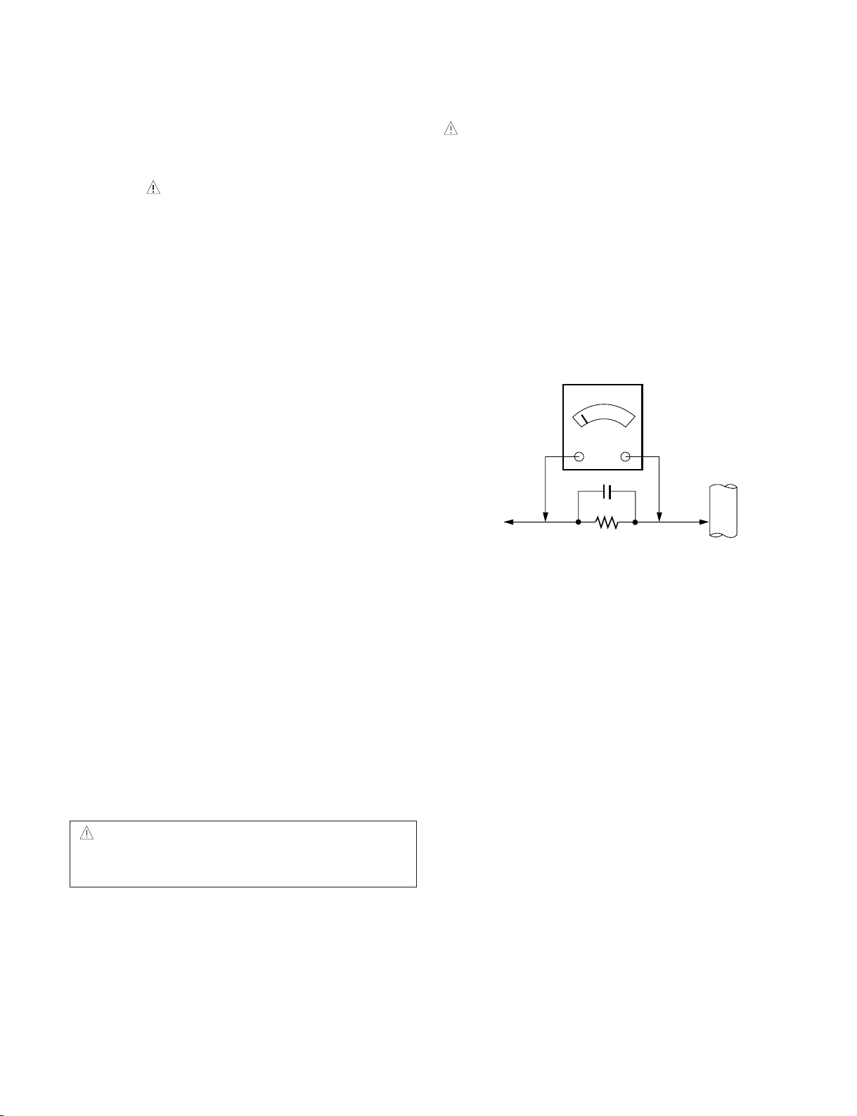
Leakage Current Hot Check Circuit
PRECAUTION
CAUTION
Please use only a plastic screwdriver to protect yourself
from shock hazard during service operation.
1.5 Kohm/10W
To Instrument's
exposed
METALLIC PARTS
Good Earth Ground
such as WATER PIPE,
CONDUIT etc.
AC Volt-meter

- 9 -
SERVICING PRECAUTIONS
CAUTION: Before servicing receivers covered by this
service manual and its supplements and addenda, read
and follow the SAFETY PRECAUTIONS on page 3 of this
publication.
NOTE: If unforeseen circumstances create conflict
between the following servicing precautions and any of the
safety precautions on page 3 of this publication, always
follow the safety precautions. Remember: Safety First.
General Servicing Precautions
1. Always unplug the receiver AC power cord from the AC
power source before;
a. Removing or reinstalling any component, circuit
board module or any other receiver assembly.
b. Disconnecting or reconnecting any receiver electrical
plug or other electrical connection.
c. Connecting a test substitute in parallel with an
electrolytic capacitor in the receiver.
CAUTION: A wrong part substitution or incorrect
polarity installation of electrolytic capacitors may
result in an explosion hazard.
d. Discharging the picture tube anode.
2. Test high voltage only by measuring it with an
appropriate high voltage meter or other voltage
measuring device (DVM, FETVOM, etc) equipped with
a suitable high voltage probe.
Do not test high voltage by "drawing an arc".
3. Discharge the picture tube anode only by (a) first
connecting one end of an insulated clip lead to the
degaussing or kine aquadag grounding system shield
at the point where the picture tube socket ground lead
is connected, and then (b) touch the other end of the
insulated clip lead to the picture tube anode button,
using an insulating handle to avoid personal contact
with high voltage.
4. Do not spray chemicals on or near this receiver or any
of its assemblies.
5. Unless specified otherwise in this service manual,
clean electrical contacts only by applying the following
mixture to the contacts with a pipe cleaner, cottontipped stick or comparable non-abrasive applicator;
10% (by volume) Acetone and 90% (by volume)
isopropyl alcohol (90%-99% strength)
CAUTION: This is a flammable mixture.
Unless specified otherwise in this service manual,
lubrication of contacts in not required.
6. Do not defeat any plug/socket B+ voltage interlocks
with which receivers covered by this service manual
might be equipped.
7. Do not apply AC power to this instrument and/or any of
its electrical assemblies unless all solid-state device
heat sinks are correctly installed.
8. Always connect the test receiver ground lead to the
receiver chassis ground before connecting the test
receiver positive lead.
Always remove the test receiver ground lead last.
9. Use with this receiver only the test fixtures specified in
this service manual.
CAUTION: Do not connect the test fixture ground strap
to any heat sink in this receiver.
Electrostatically Sensitive (ES) Devices
Some semiconductor (solid-state) devices can be
damaged easily by static electricity. Such components
commonly are called Electrostatically Sensitive (ES)
Devices. Examples of typical ES devices are integrated
circuits and some field-effect transistors and
semiconductor "chip" components. The following
techniques should be used to help reduce the incidence of
component damage caused by static by static electricity.
1. Immediately before handling any semiconductor
component or semiconductor-equipped assembly, drain
off any electrostatic charge on your body by touching a
known earth ground. Alternatively, obtain and wear a
commercially available discharging wrist strap device,
which should be removed to prevent potential shock
reasons prior to applying power to the unit under test.
2. After removing an electrical assembly equipped with
ES devices, place the assembly on a conductive
surface such as aluminum foil, to prevent electrostatic
charge buildup or exposure of the assembly.
3. Use only a grounded-tip soldering iron to solder or
unsolder ES devices.
4. Use only an anti-static type solder removal device.
Some solder removal devices not classified as "antistatic" can generate electrical charges sufficient to
damage ES devices.
5. Do not use freon-propelled chemicals. These can
generate electrical charges sufficient to damage ES
devices.
6. Do not remove a replacement ES device from its
protective package until immediately before you are
ready to install it. (Most replacement ES devices are
packaged with leads electrically shorted together by
conductive foam, aluminum foil or comparable
conductive material).
7. Immediately before removing the protective material
from the leads of a replacement ES device, touch the
protective material to the chassis or circuit assembly
into which the device will be installed.
CAUTION: Be sure no power is applied to the chassis
or circuit, and observe all other safety precautions.
8. Minimize bodily motions when handling unpackaged
replacement ES devices. (Otherwise harmless motion
such as the brushing together of your clothes fabric or
the lifting of your foot from a carpeted floor can
generate static electricity sufficient to damage an ES
device.)

- 10 -
General Soldering Guidelines
1. Use a grounded-tip, low-wattage soldering iron and
appropriate tip size and shape that will maintain tip
temperature within the range or 500
F to 600 F.
2. Use an appropriate gauge of RMA resin-core solder
composed of 60 parts tin/40 parts lead.
3. Keep the soldering iron tip clean and well tinned.
4. Thoroughly clean the surfaces to be soldered. Use a
mall wire-bristle (0.5 inch, or 1.25cm) brush with a
metal handle.
Do not use freon-propelled spray-on cleaners.
5. Use the following unsoldering technique
a. Allow the soldering iron tip to reach normal
temperature.
(500
F to 600 F)
b. Heat the component lead until the solder melts.
c. Quickly draw the melted solder with an anti-static,
suction-type solder removal device or with solder
braid.
CAUTION: Work quickly to avoid overheating the
circuitboard printed foil.
6. Use the following soldering technique.
a. Allow the soldering iron tip to reach a normal
temperature (500
F to 600 F)
b. First, hold the soldering iron tip and solder the strand
against the component lead until the solder melts.
c. Quickly move the soldering iron tip to the junction of
the component lead and the printed circuit foil, and
hold it there only until the solder flows onto and
around both the component lead and the foil.
CAUTION: Work quickly to avoid overheating the
circuit board printed foil.
d. Closely inspect the solder area and remove any
excess or splashed solder with a small wire-bristle
brush.
IC Remove/Replacement
Some chassis circuit boards have slotted holes (oblong)
through which the IC leads are inserted and then bent flat
against the circuit foil. When holes are the slotted type,
the following technique should be used to remove and
replace the IC. When working with boards using the
familiar round hole, use the standard technique as
outlined in paragraphs 5 and 6 above.
Removal
1. Desolder and straighten each IC lead in one operation
by gently prying up on the lead with the soldering iron
tip as the solder melts.
2. Draw away the melted solder with an anti-static
suction-type solder removal device (or with solder
braid) before removing the IC.
Replacement
1. Carefully insert the replacement IC in the circuit board.
2. Carefully bend each IC lead against the circuit foil pad
and solder it.
3. Clean the soldered areas with a small wire-bristle
brush. (It is not necessary to reapply acrylic coating to
the areas).
"Small-Signal" Discrete Transistor
Removal/Replacement
1. Remove the defective transistor by clipping its leads as
close as possible to the component body.
2. Bend into a "U" shape the end of each of three leads
remaining on the circuit board.
3. Bend into a "U" shape the replacement transistor leads.
4. Connect the replacement transistor leads to the
corresponding leads extending from the circuit board
and crimp the "U" with long nose pliers to insure metal
to metal contact then solder each connection.
Power Output, Transistor Device
Removal/Replacement
1. Heat and remove all solder from around the transistor
leads.
2. Remove the heat sink mounting screw (if so equipped).
3. Carefully remove the transistor from the heat sink of the
circuit board.
4. Insert new transistor in the circuit board.
5. Solder each transistor lead, and clip off excess lead.
6. Replace heat sink.
Diode Removal/Replacement
1. Remove defective diode by clipping its leads as close
as possible to diode body.
2. Bend the two remaining leads perpendicular y to the
circuit board.
3. Observing diode polarity, wrap each lead of the new
diode around the corresponding lead on the circuit
board.
4. Securely crimp each connection and solder it.
5. Inspect (on the circuit board copper side) the solder
joints of the two "original" leads. If they are not shiny,
reheat them and if necessary, apply additional solder.
Fuse and Conventional Resistor
Removal/Replacement
1. Clip each fuse or resistor lead at top of the circuit board
hollow stake.
2. Securely crimp the leads of replacement component
around notch at stake top.
3. Solder the connections.
CAUTION: Maintain original spacing between the
replaced component and adjacent components and the
circuit board to prevent excessive component
temperatures.

- 11 -
Circuit Board Foil Repair
Excessive heat applied to the copper foil of any printed
circuit board will weaken the adhesive that bonds the foil
to the circuit board causing the foil to separate from or
"lift-off" the board. The following guidelines and
procedures should be followed whenever this condition is
encountered.
At IC Connections
To repair a defective copper pattern at IC connections use
the following procedure to install a jumper wire on the
copper pattern side of the circuit board. (Use this
technique only on IC connections).
1. Carefully remove the damaged copper pattern with a
sharp knife. (Remove only as much copper as
absolutely necessary).
2. carefully scratch away the solder resist and acrylic
coating (if used) from the end of the remaining copper
pattern.
3. Bend a small "U" in one end of a small gauge jumper
wire and carefully crimp it around the IC pin. Solder the
IC connection.
4. Route the jumper wire along the path of the out-away
copper pattern and let it overlap the previously scraped
end of the good copper pattern. Solder the overlapped
area and clip off any excess jumper wire.
At Other Connections
Use the following technique to repair the defective copper
pattern at connections other than IC Pins. This technique
involves the installation of a jumper wire on the
component side of the circuit board.
1. Remove the defective copper pattern with a sharp
knife.
Remove at least 1/4 inch of copper, to ensure that a
hazardous condition will not exist if the jumper wire
opens.
2. Trace along the copper pattern from both sides of the
pattern break and locate the nearest component that is
directly connected to the affected copper pattern.
3. Connect insulated 20-gauge jumper wire from the lead
of the nearest component on one side of the pattern
break to the lead of the nearest component on the
other side.
Carefully crimp and solder the connections.
CAUTION: Be sure the insulated jumper wire is
dressed so the it does not touch components or sharp
edges.
DISASSEMBLY
- 12 -
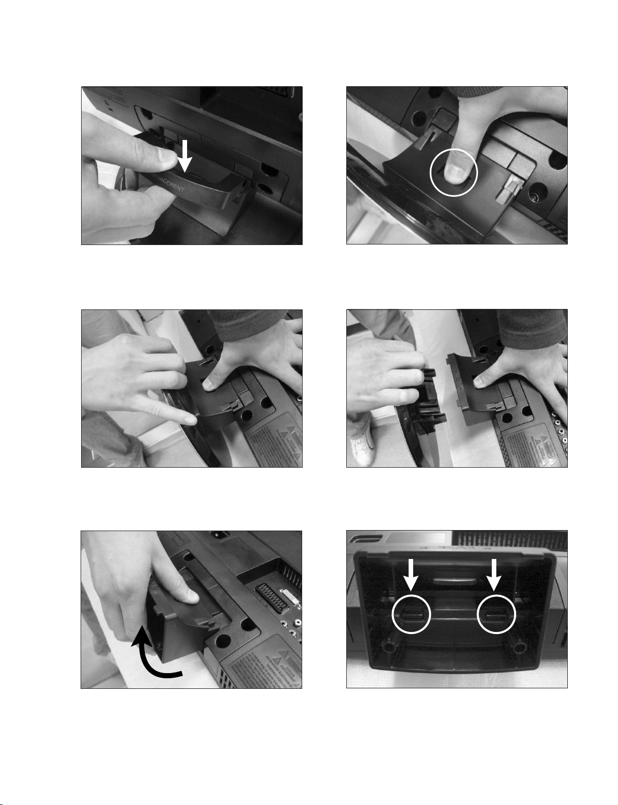
1. Push down slightly to disassembly it.
2. After push the cable management like above fig.(Downward),
Disassembly the Cable management with pulling it upward.
3. Disassembly Cable Holder.
Disassembly Stand base.
Remove base body Like a picture.
Push 2 letches Like a picture.
Push the button.
Hold the stand base.
# 1
# 4
# 2
# 5
# 3
# 6
- 13 -
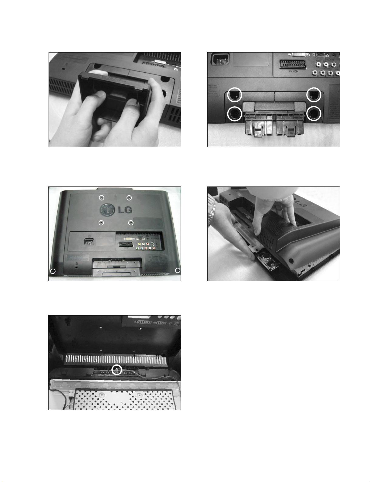
# 7
# 9
# 8
# 10
Pull base body to separate from set during pressing 2 letches.
Remove the screws.
# 11
Pull the connector.
Disassembly back cover.
1. Remove the screws.
2. Disassembly Hinge Cover.

- 14 -
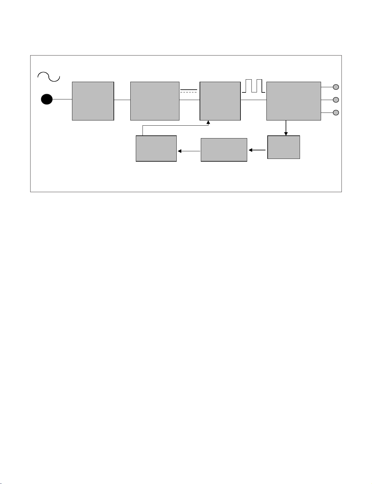
BLOCK DIAGRAM
Data
16Mb
(FSD 0 ..31)
(FSA 0 ..11)
LCD
Module
SDRAM
(HY57V161610FTP)
LVDS Signal
(CMO)
4Mb
Flash
Serial
Data
(OCMD 0 ..7)
(OCMA 0 ..19)
Memory
(MX25L4005A)
EEPROM
System(64k)
SP (L)
L
SP (R)
Amp
Audio
R
(YDA138)
EAGLE EYE
POWER IR
INPUT MENU OK VOL PR
EEPROM
TMDS Signal
DVI-D
Scaler+Video
Y/Pb/Pr
EEPROM
Analog Signal (R/G/B/H/V)
COMP
D-SUB
Decorder
(LGE9789AD-LF)
(DAC)
CS4351
R/G/B/CVBS/Audio
SCART
CVBS/Audio
Y/C
CVBS
SIF
CVBS
Tuner
TAFT-W003D
L/R
L/R
CVBS Audio
COMP Audio
L/R
PC Audio

- 15 -
DESCRIPTION OF BLOCK DIAGRAM
1. Power Supply Block (LIPS)
This Block Generates DC Voltage (5V,15V) to Main Control system from AC Power (100-240 V, 50/60 Hz, 1.0A)
2. DC/DC Converter block
DC/DC Converter convert the input 5V,15V to proper 1.8V,2.5V,3.3V,5V,10.5V for Main control system.
For shooting heat trouble, we use the DC/DC converting IC
3. Scaler + Video/Audio decorder (Scaler IC, LGE9789AD-LF)
It is composed of LGE9789AD-LF.
It includes AD Converter, LVDS/TMDS Transmitter, Micom, and Audio processor.
1) Video Signal - CVBS/S-Video/Component/RGB/DVI(TMDS)
This Block Selects input Video signals (like CVBS, Y/C, SCART RGB) and output RGB signal.
On decoding, We can control signal like Contrast, Brightness, Sharpness, Color, tint signals including Adaptive
Comb Filter.
2) Audio Signal
This block analyzes audio input signal through A/V Jack and PC audio and Tuner IF.
The analyzed signals transmitted to audio amplifier (YDA138)
On decoding, We can control signal like Bass, treble.
4. Flash Memory(MX25L4005A)
This is composed of MX25L4005A.
This store the source data of micom.
5. Tuner
Micom controls this IC through IIC line.
Tuner makes CVBS and transmits IF signal to LGE9789AD-LF.
6. Audio Amplifier (YDA138)
This block is composed of YDA138 and peripheral device.
The function of the audio amplifier is that to amplify audio L / R signal transmitted from audio decoder.
The audio signal is amplified according to pre-defined DC volume control curve.
Also, headphone amplifier is included at this IC.
- 16 -
LIPS Board Block Diagram
Operation description_LIPS
1. EMI components.
This part contains of EMI components to comply with global marketing EMI standards like FCC,VCCI CISPR, the
circuit included a line-filter, across line capacitor and of course the primary protection fuse.
2. Input rectifier and filter.
This part function is for transfer the input AC voltage to a DC voltage through a bridge rectifier and a bulk capacitor.
3. Energy Transfer.
This part function is for transfer the primary energy to secondary through a power transformer.
4. Output rectifier and filter.
This part function is to make a pulse width modulation control and to provide the driver signal to power switch, to
adjust the duty cycle during different AC input and output loading condition to achieve the dcoutput stabilized, and also
the over power protection is also monitor by this part.
5. Photo-Coupler isolation.
This part function is to feed back the DC output changing status through a photo transistor to primary controller to
achieve the stabilized DC output voltage.
6. Signal collection.
This part function is to collect the any change from the DC output and feed back to the primary through photo
transistor.
50 ~ 60Hz
100KHz
OUTPUT RECTIFIER
AND FILTER
LINE
EMI
COMPONENTS
INPUT RECTIFIER
AND FILTER
HVDC
ENERGY
TRANSFER
100 ~ 240V
PWM
CONTROL
CIRCUIT
PHOTO
-COUPLER
ISOLATION
SIGNAL
COLLENT-
ION
PRIMARY SECONDARY
15V
5V
GND
 Loading...