

Page 1

MP3 CD
MICRO SYSTEM
SERVICE MANUAL
SERVICE MANUAL MODEL: FFH-M217X, FE-M217E
CAUTION
BEFORE SERVICING THE UNIT, READ THE “SUMMARY” IN THIS MANUAL.
MODEL: FFH-M217X, FE-M217E
Page 2

- 1-1 -
[CONTENTS]
❍ SECTION 1. GENERAL
• SERVICING PRECAUTIONS
.....................................................................................................
1-2
• ESD PRECAUTIONS
.................................................................................................................
1-4
• SPECIFICATION
........................................................................................................................
1-5
❍ SECTION 2. ELECTRICAL SECTION
• ADJUSTMENTS
.........................................................................................................................
2-1
• TROUBLESHOOTING ............................................................................................................... 2-2
• WAVEFORMS OF MAJOR CHECK POINT............................................................................. 2-18
• INTERNAL BLOCK DIAGRAM OF ICs .................................................................................... 2-20
• BLOCK DIAGRAM
....................................................................................................................
2-25
• SCHEMATIC DIAGRAMS
........................................................................................................
2-27
• WIREING DIAGRAM ................................................................................................................ 2-29
• PRINTED CIRCUIT DIAGRAMS .............................................................................................. 2-33
❍ SECTION 3. EXPLODED VIEWS
• CABINET AND MAIN FRAME SECTION
..................................................................................
3-1
• TAPE DECK MECHANISM: SINGLE AUTO REVERSE DECK
.................................................
3-3
• OPTION PICK-UP CARRIAGE
...................................................................................................
3-5
❍ SECTION 4. SPEAKER PART
• SPEAKER PART
........................................................................................................................
4-1
❍ SECTION 5. REPLACEMENT PARTS LIST
• REPLACEMENT PARTS LIST
....................................................................................................
5-1
Page 3
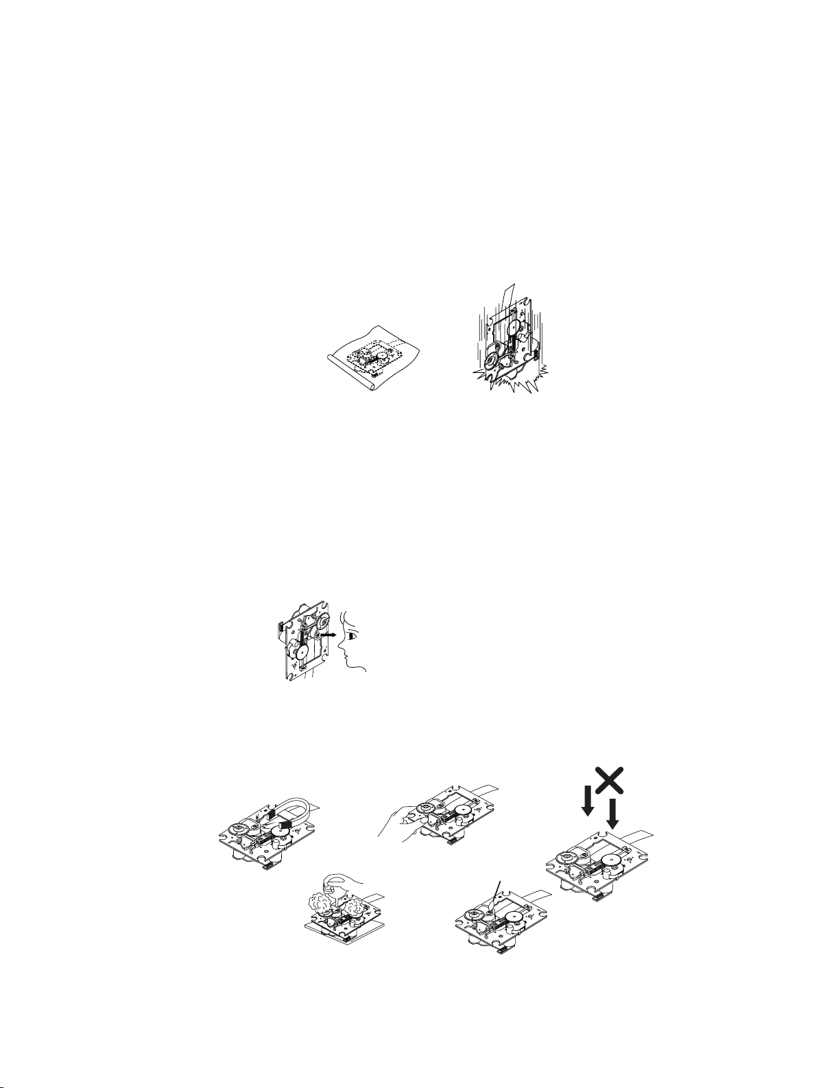
❏ SERVICING PRECAUTIONS
NOTES REGARDING HANDLING OF THE PICK-UP
1. Notes for transport and storage
1) The pick-up should always be left in its conductive bag until immediately prior to use.
2) The pick-up should never be subjected to external pressure or impact.
2. Repair notes
1) The pick-up incorporates a strong magnet, and so should never be brought close to magnetic materials.
2) The pick-up should always be handled correctly and carefully, taking care to avoid external pressure and
impact. If it is subjected to strong pressure or impact, the result may be an operational malfunction and/or
damage to the printed-circuit board.
3) Each and every pick-up is already individually adjusted to a high degree of precision, and for that reason
the adjustment point and installation screws should absolutely never be touched.
4) Laser beams may damage the eyes!
Absolutely never permit laser beams to enter the eyes!
Also NEVER switch ON the power to the laser output part (lens, etc.) of the pick-up if it is damaged.
5) Cleaning the lens surface
If there is dust on the lens surface, the dust should be cleaned away by using an air bush (such as used
for camera lens). The lens is held by a delicate spring. When cleaning the lens surface, therefore, a
cotton swab should be used, taking care not to distort this.
6) Never attempt to disassemble the pick-up.
Spring by excess pressure. If the lens is extremely dirty, apply isopropyl alcohol to the cotton swab. (Do
not use any other liquid cleaners, because they will damage the lens.) Take care not to use too much of
this alcohol on the swab, and do not allow the alcohol to get inside the pick-up.
-1-2-
Storage in conductive bag
Drop impact
NEVER look directly at the laser beam, and don’t let
contact fingers or other exposed skin.
Magnet
Howtoholdthepick-up
Pressure
Pressure
Cotton swab
Conductive Sheet
SECTION 1. GENERAL
Page 4
NOTES REGARDING COMPACT DISC PLAYER REPAIRS
1. Preparations
1) Compact disc players incorporate a great many ICs as well as the pick-up (laser diode). These
components are sensitive to, and easily affected by, static electricity. If such static electricity is high
voltage, components can be damaged, and for that reason components should be handled with care.
2) The pick-up is composed of many optical components and other high-precision components. Care must
be taken, therefore, to avoid repair or storage where the temperature of humidity is high, where strong
magnetism is present, or where there is excessive dust.
2. Notes for repair
1) Before replacing a component part, first disconnect the power supply lead wire from the unit
2) All equipment, measuring instruments and tools must be grounded.
3) The workbench should be covered with a conductive sheet and grounded.
When removing the laser pick-up from its conductive bag, do not place the pick-up on the bag. (This is
because there is the possibility of damage by static electricity.)
4) To prevent AC leakage, the metal part of the soldering iron should be grounded.
5) Workers should be grounded by an armband (1MΩ)
6) Care should be taken not to permit the laser pick-up to come in contact with clothing, in order to prevent
static electricity changes in the clothing to escape from the armband.
7) The laser beam from the pick-up should NEVER be directly facing the eyes or bare skin.
CLEARING MALFUNCTION
You can reset your unit to initial status if malfunction occur(button malfunction, display, etc.).
Using a pointed good conductor(such as driver), simply short the RESET jump wire on the inside of the
volume knob for more than 3 seconds.
If you reset your unit, you must reenter all its settings(stations, clock, timer)
NOTE: 1. To operate the RESET jump wire, pull the volume rotary knob and release it.
2. If you wish to operate the RESET jump wire, it is necessary to unplug the power cord.
- 1-3 -
Armband
Conductive
Sheet
Resistor
(1 Mohm)
Resistor
(1 Mohm)
VOLUME KNOB
UP
DOWN
VOLUME
RESET jump wire
RESET
Page 5
❐ ESD PRECAUTIONS
Electrostatically Sensitive Devices (ESD)
Some semiconductor (solid state) devices can be damaged easily by static electricity. Such components
commonly are called Electrostatically Sensitive Devices (ESD). Examples of typical ESD devices are integrated
circuits and some field-effect transistors and semiconductor chip components. The following techniques should
be used to help reduce the incidence of component damage caused by static electricity.
1. Immediately before handling any semiconductor component or semiconductor-equipped assembly, drain off
any electrostatic charge on your body by touching a known earth ground. Alternatively, obtain and wear a
commercially available discharging wrist strap device, which should be removed for potential shock reasons
prior to applying power to the unit under test.
2. After removing an electrical assembly equipped with ESD devices, place the assembly on a conductive
surface such as aluminum foil, to prevent electrostatic charge buildup or exposure of the assembly.
3. Use only a grounded-tip soldering iron to solder or unsolder ESD devices.
4. Use only an anti-static solder removal device. Some solder removal devices not classified as "anti-static" can
generate electrical charges sufficient to damage ESD devices.
5. Do not use freon-propelled chemicals. These can generate electrical charges sufficient to damage ESD
devices.
6. Do not remove a replacement ESD device from its protective package until immediately before you are ready
to install it. (Most replacement ESD devices are packaged with leads electrically shorted together by
conductive foam, aluminum foil or comparable conductive materials).
7. Immediately before removing the protective material from the leads of a replacement ESD device, touch the
protective material to the chassis or circuit assembly into which the device will by installed.
CAUTION : BE SURE NO POWER IS APPLIED TO THE CHASSIS OR CIRCUIT, AND OBSERVE ALL OTHER
SAFETY PRECAUTIONS.
8. Minimize bodily motions when handing unpackaged replacement ESD devices. (Otherwise harmless motion
such as the brushing together of your clothes fabric or the lifting of your foot from a carpeted floor can
generate static electricity sufficient to damage an ESD device).
[CAUTION. GRAPHIC SYMBOLS]
-1-4-
THE LIGHTNING FLASH WITH APROWHEAD SYMBOL. WITHIN AN EQUILATERAL
TRIANGLE, IS INTENDED TO ALERT THE SERVICE PERSONNEL TO THE PRESENCE
OF UNINSULATED “DANGEROUS VOLTAGE” THAT MAY BE OF SUFFICIENT
MAGNITUDE TO CONSTITUTE A RISK OF ELECTRIC SHOCK.
THE EXCLAMATION POINT WITHIN AN EQUILATERAL TRIANGLE IS INTENDED TO
ALERT THE SERVICE PERSONNEL TO THE PRESENCE OF IMPORTANT SAFETY
INFORMATION IN SERVICE LITERATURE.
Page 6
❏ SPECIFICATIONS
- 1-5 -
General Power supply Refer to the back panel of the unit
Power consumption 50W
Mass 4.2kg
Extemal dimensions(W X H X D)
161 X 249 X 275mm
CD Frequency Response 40 -18000Hz
Signal-to-noise ratio 70dB
Dynamic range 70dB
Tuning Range 87.5 -108.0MHz or 65 ~ 74MHz, 87.5 ~108.0 MHz
Intermediate Frequency 10.7 MHz
FM Signal-to-noise ratio 60/55 dB
Frequency Response 60 -10000Hz
Tuning Range 522-1620kHz or 520-1720kHz
AM Intermediate Frequency 450kHz
Signal-to-noise ratio 35 dB
Frequency Response 100 -1800 Hz
AMP Output Power 20W + 20W
T.H.D 0.2%
Frequency Response 40-25000Hz
Signal-to-noise ratio 80dB
TAPE Tape Speed 3000 ± 3% (MTT-111, NORMAL-SPEED)
Wow Flutter 0.25% (MTT-111,JIS-WTD)
F.F/REW Time 120sec(C-60)
Frequency Response 250-8000Hz
Signal-to-noise ratio 43dB(P/B)/43dB(R/P)
Channel Separation 50dB(P/B)/45dB(R/P)
Erase Ratio 55dB (MTT-5511)
Speaker Type 2 Way 2 Speaker
Impedance 6Ω
Frequency Response 85-20000Hz
Sound Pressure Level 88dB/W(1m)
Rated Input Power 20W
Max.Input Power 40W
Net Dimension(W
X H X D) 153 X 240 X 220mm
Net Weight(1EA) 2.24kg
NOTE : Specification are subject to change without notice in the course of product improvement.
TUNER
Page 7

-1-6-
Page 8
- 2-1 -
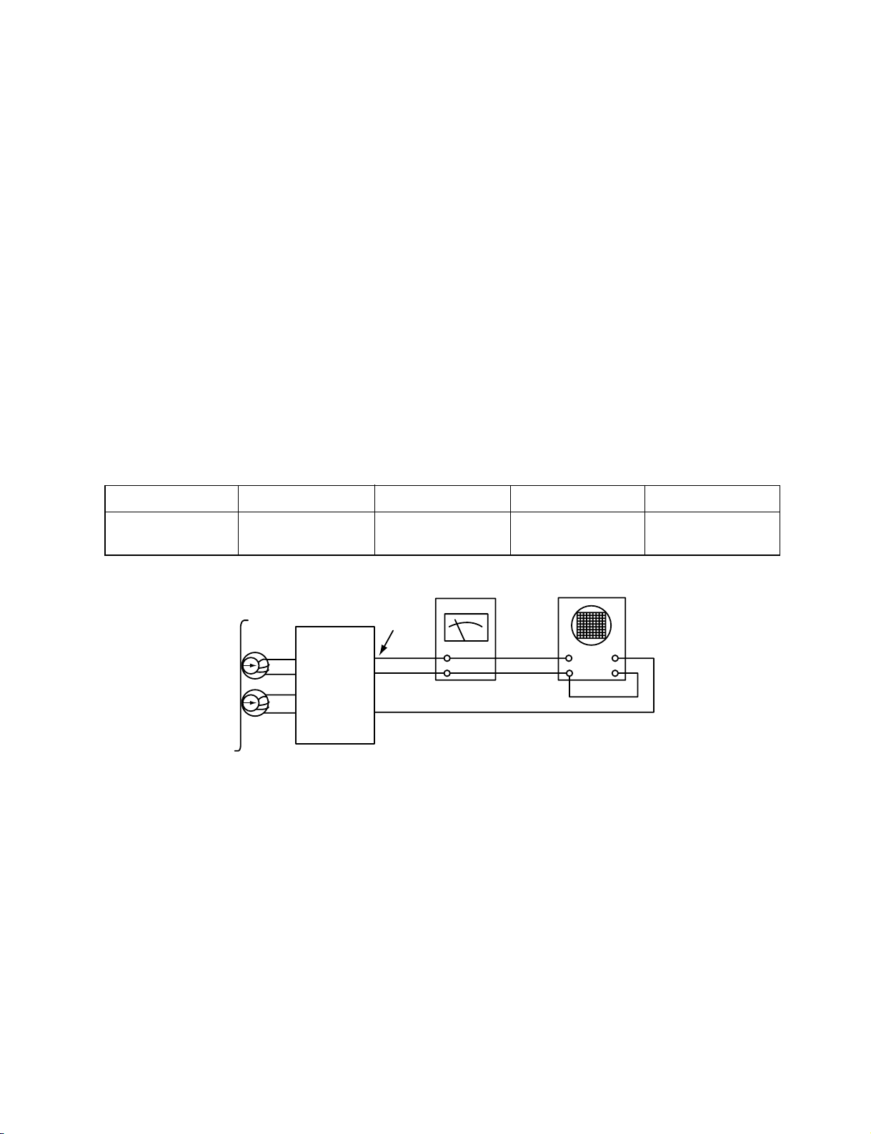
TAPE DECK ADJUSTMENT
1. AZIMUTH ADJUSTMENT
Figure 1. Azimuth Adjustment Connection Diagram
CH1 CH2
Speaker Out
Playback Mode
Head
Test Tape
MTT-114
L ch
R ch
GND
Dual-trace
synchroscope
Electronic
Voltmeter
L out
R out
Unit
❏ ADJUSTMENTS
This set has been aligned at the factory and normally will not require further adjustment. As a result, it is not
recommended that any attempt is made to modificate any circuit. If any parts are replaced or if anyone tampers
with the adjustment, realignment may be necessary.
IMPORTANT
1. Check Power-source voltage.
2. Set the function switch to band being aligned.
3. Turn volume control to minimum unless otherwise noted.
4. Connect low side of signal source and output indicator to chassis ground unless otherwise specified.
5. Keep the signal input as low as possible to avoid AGC and AC action.
Deck Mode Test Tape Test Point Adjustment Adjust for
Palyback MTT-114 Speaker Out
DECK Screw
Maximum
Azimuth Screw
SECTION 2. ELECTRICAL SECTION
Page 9
-2-2-
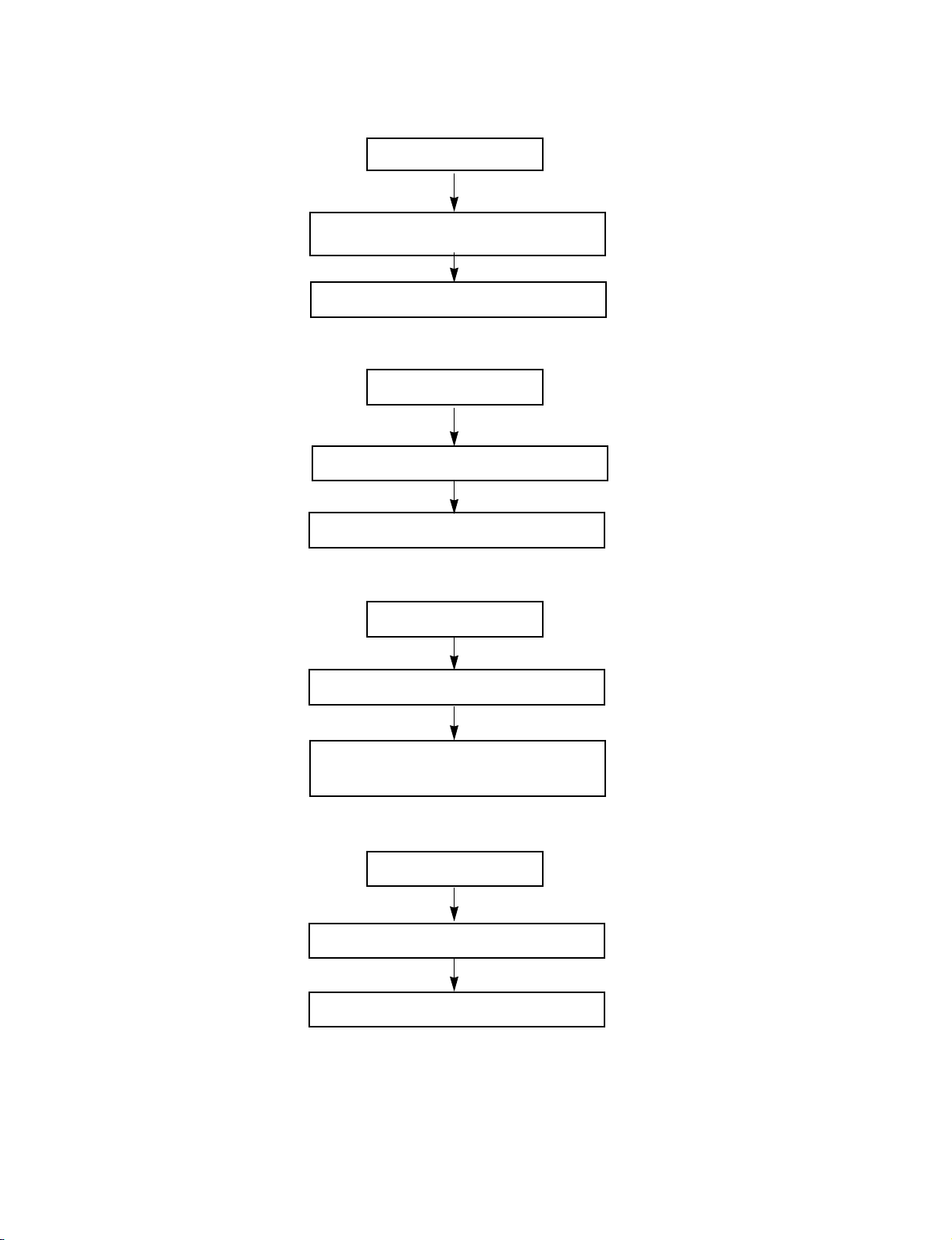
❏ TROUBLESHOOTING
• AUDIO PART
VKK PART
Does DC - 33V appear at
PN301 pin .
Check the pattern of FRONT
PCB ASS’Y
Check the DC -35V of C928(-)
Check the DC -33V of
ZD 902(-)
Check the DC -33V of
Q901 “E”
Check the PATTERN
Replace the D936
Replace the ZD902
Replace the Q901
YES
YES
YES
YES
NO
NO
NO
NO
P-SENS PART
Does +5V appear at ZD901?
Check the pattern of
IC301 pin .
Check the waveform
of D937 (+).
Replace ZD901.
Replace the D937
YES
YES
NO
NO
26
19
Page 10
- 2-3 -
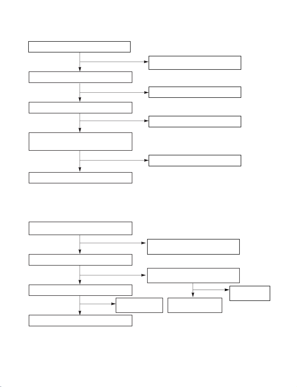
POWER CIRCUIT
Check the Fuse
Check the DC output
of C921(+)
Check the DC 12V
Output of IC901
Check the DC 6.2V
output of IC902
Check the DC 12V
Output of IC903
Check the 5.6V of Q604 “C”
(CD FUNCTION)
END
Replace the Fuse
CHECK THE AC VOLTAGE
OF CN901
pin
1, 4
Replace the IC903
Replace the D921, D922,
D923, D924
Replace the IC902
Check DC VOLTAGE OF
D930(+)
Check the “High” of
IC903 pin4
Check the “High” of Q605“B”
Replace the Q604
Replace the IC902
Replace the Transformer
Replace the D930
Check the "High" of
PN601 pin5
Check the “High” of
IC601 pin12
YES
YES
YES
YES
YES
YES
YES
YES
YES
YES
NO
NO
NO
NO
NO
NO
NO
NO
NO
NO
Page 11
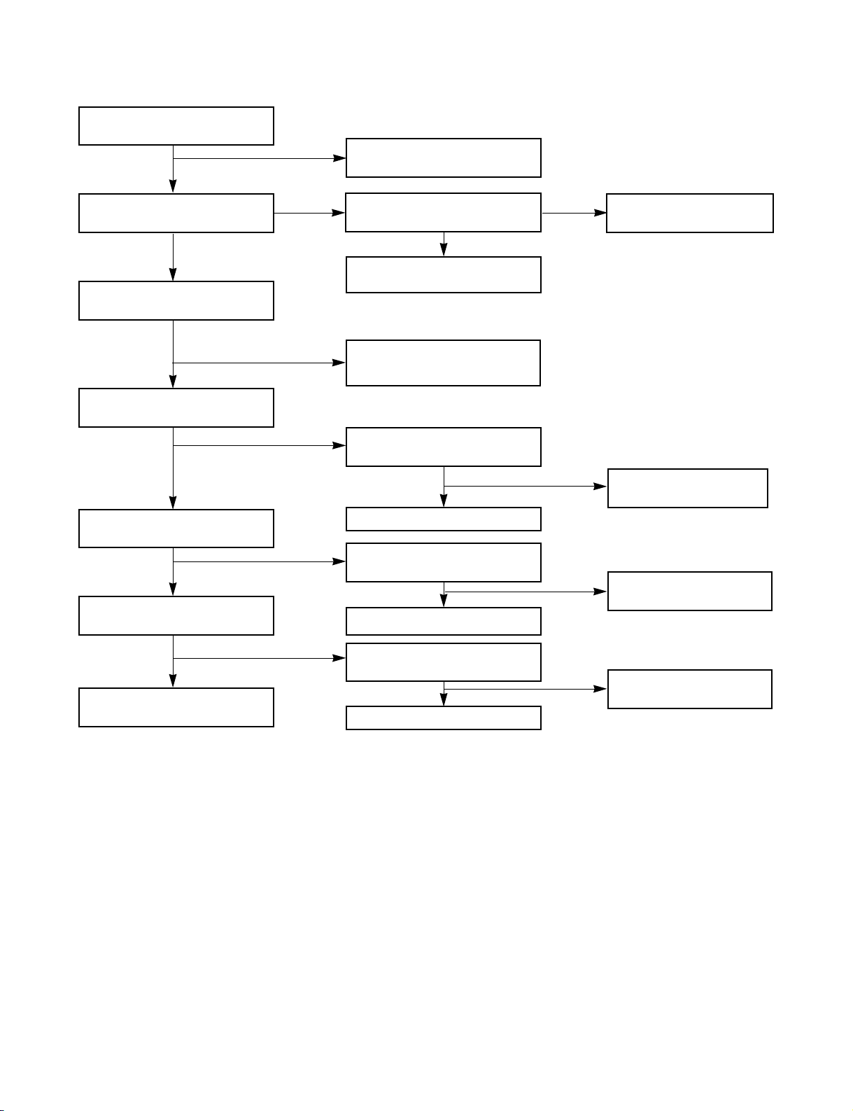
-2-4-
AUDIO ABNORMAL
Check the signal output of
IC701 pin2, 4
Check the signal input of IC701
pin7, 11
Check the DC +9V of IC601
pin1
Check the “High” of Q702 “B”
Check the “High” of
IC701 pin5
Check the power of IC701
Check the connecting to
SPEAKER
YES
YES
YES
NO
NO
NO
MUTING CIRCUIT (MUTE)
Dose “High” appear at
Q701, Q751“B”
check the “Low” of Q701,
Q751, “C”
MUTE
Check the “High” of PN601 pin4
Check the “High” of
the IC301 pin12
Replace the Q703
Replace the TR
Refer to IC 301
Troubleshooting
YES
YES
YES
NO
NO
NO
Page 12
- 2-5 -
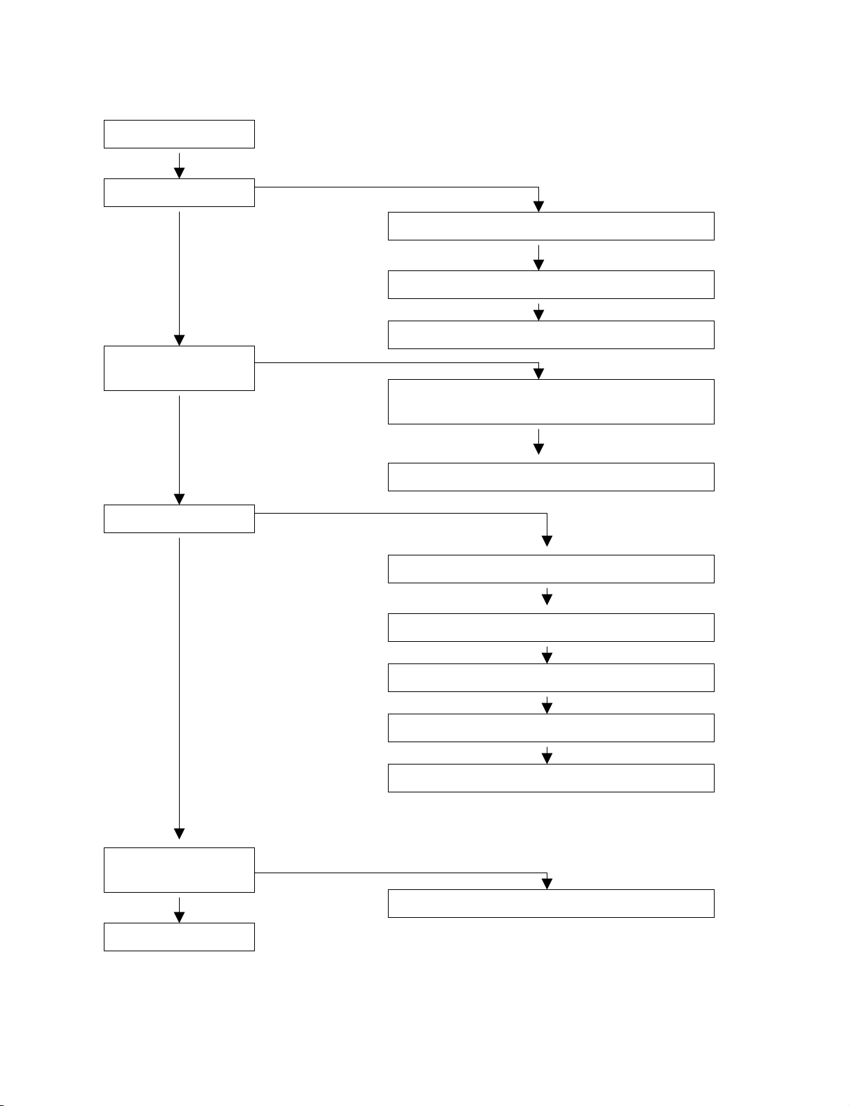
FUNCTION MODE AUDIO ABNORMAL
TAPE
Check the signal input
of IC601 pin6, 23
Refer to “IC201 Troubleshooting”
AUX
Chekc the signal input of IC601,
pin
5, 24
Check the signal input of JK601
Check the signal input of IC601
pin
3, 26
Check the signal input of PN603 pin6, 8
Check the signal input of IC601 pin4, 25
Refer to “TUNER PACK Troubleshooting”
CD
TUNER
Page 13
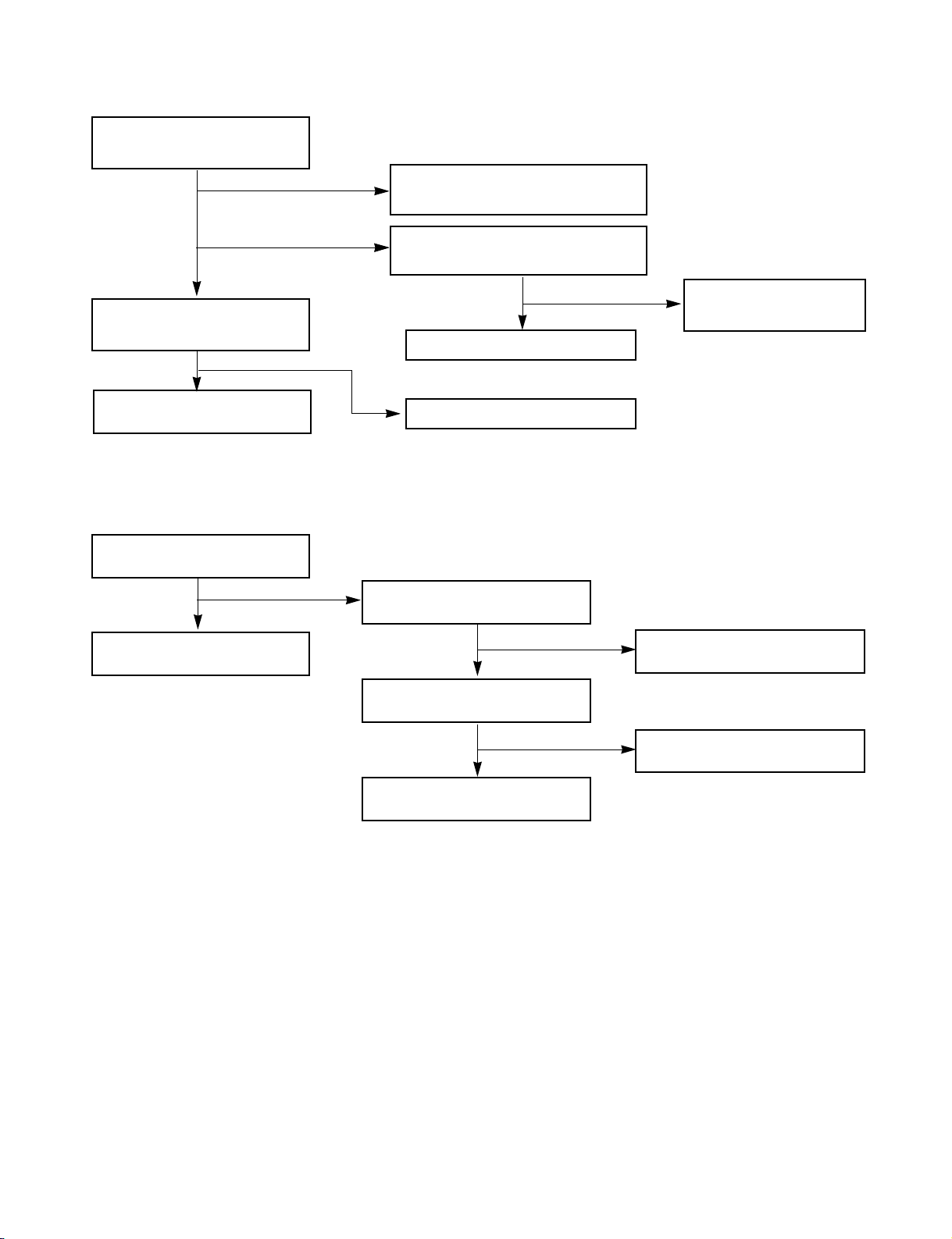
-2-6-
Refer to “IC301
Troubleshooting”
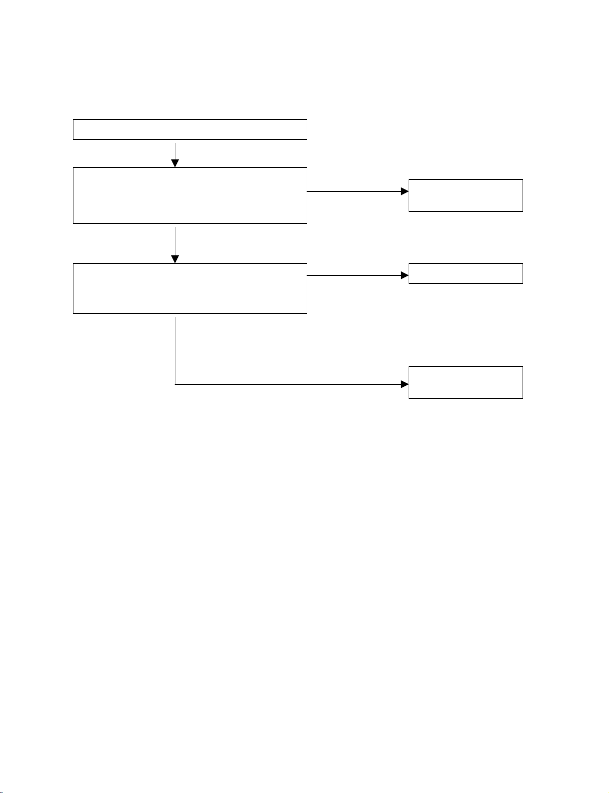
IC301 TROUBLESHOOTING
IC601 TROUBLESHOOTING
Check the power supplying IC301
pin
31,32,51,88?
Refer to “Power Circuit Troubleshooting”
Check the P-SENS
Replace the X301
Check the RESET circuit
Refer to “Power Circuit Troubleshooting”
Check the Data of IC301 pin14, 15
(CD ➞ TAPE FUNCTION)
Replace the
IC601
Check the pattern
Check the P-SENS “High” of IC301 pin6
Check the oscillation of X301
When power supplying to IC301 pin92.
(Low ➞ High)
Replace the IC301
Check the power supplying
to IC601 pin1
Check the CLK Data of IC601 pin14, 15
Check the IC601 FUNCTION SELECTOR
END
YES
YES
YES
YES
YES
YES
YES
NO
NO
NO
NO
NO
NO
NO
Page 14

- 2-7 -
TUNER PACK TROUBLESHOOTING
Check the PLL- of CE, DI, DO, CLK
Is the normal ?
END
CE: Chip Enable
DI: Data Input(from u-com)
DO: Data Output(to u-com)
CLK: Tuner mode clock
Replace the TUNER PACK
YES
NO
TUNER PACK POWER TROUBLESHOOTING
Check the +9V of TU601 pin2
Check the +DC C670
Check the pattern
Refer to “Power circuit
Troubleshooting”
Check the GND of TU601 pin4, 10
END
YES
YES
YES
NO
NO
PLAY
Check the VCC supplying to IC201 pin4
Refer to “Power Circuit
Troubleshooting”
Check the Deck Mecha
Replace the Deck
Mecha.
Replace the IC201
Check the signal output of IC201 pin3, 6
Check the “LOW” of Q201, Q251, “B”
YES
YES
YES
NO
NO
NO
Page 15

-2-8-
REC (Q252, Q202 ON / R273, R223 HIGH)
Check signal supplied to IC203 pin2, 8 ?
Check the output of IC203 pin3, 7
Check the “voltage” of L201 pin5
Refer to “power circuit Troubleshooting”
Check the power
supplying to C227(+)
Check the oscillation
of Q204, “E”
Check the signal of
R212, R262
Check the Pattern
Check the Vcc power of IC203 Pin6
Check the oscillation of L201 pin 1, 3
Replace the DECK
Check the “Low” of Q202,
Q252 “B”
Replace the Q202, Q252
Check the “Low” of
PN601 pin14
Refer to
“Power Circuit
Troubleshooting”
Check the 0.6V of
Q205 “B”
Replace the L201
YES
YES
YES
YES
YES
YES
YES
YES
NO
NO
NO
NO
NO
NO
NO
NO
Page 16
- 2-9 -
•CDPART
TURN ON CD
OPEN CLOSE CHECK
CONNECTOR CHECK ( PN508,PN507)
CHECK POWER SUPPLY CIRCUIT( PN508)
CHECK MICOM INTERFACE CIRCUIT( PN507)
CHECK MICOM INTERFACE CIRCUIT( PN507)
CONNECTOR CHECK(PN501,PN503)
CHECK PICKUP MOVEMENT
CHECK BA5810FP (IC503)
CHECK MN6627933CG (IC501)
CHECK AN22004 (IC502)
CONNECTOR CHECK (PN508)
CONNECTOR CHECK
( PN508,PN507,PN503,PN501)
“ READING ”
DISPLAY CHECK
READING OK CHECK
IF PLAY, AUDIO
OUTPUT CHECK
OK
Page 17
-2-10-
OPEN CLOSE NG
CONNECTOR LOCKING CHECK ( PN508,PN507)
DEFECTIVE MAIN
POEWR SUPPLY
DEFECTIVE MICOM
DEFECTIVE
MECHANISM
CHECK POWER SUPPLY CIRCUIT( PN508 ,PN507)
PN 508 PIN 8 = 6.2V, PIN 7 = 5V
PN507 PIN 1 = 5V
CHECK VOLTAGE CHANGE OF AD 5V, CLOSE ,
AND BTLMUTE VOLTAGE(= 5V)
(PN507 PIN 1:5V, 2:CLOSE, 3:BTLMUTE)
Page 18

- 2-11 -
“ READING ” DISPLAY CHECK (= ONLY “CD “DISPLAY)
CONNECTOR LOCKING CHECK
(PN508,PN507,PN503,PN501 )
DEFECTIVE CONNECTOR OR
MAIN POWER SUPPLAY
DEFECTIVE IC505
DEFECTIVE MICOM OR
CONNECTOR
DEFECTIVE MICOM OR
CONNECTOR
DEFECTIVE IC801
CHECK VOLTAGE THE PIN 2 OF IC505
IC505 PIN2 : 3.3V
CHECK MICOM INTERFACE
CIRCUIT( PN507 )
PN507 PIN 6,8,9,10 SIGNAL CHECK
(6: STAT, 8: MDATA, 9:MCLK, 10:MLD)
CHECK THE WAVE FORM #1
CHECK RESET SIGNAL OF PN507
PN507 PIN7 : 5V
CHECK POWER SUPPLY
PORT( PN508 ,PN507)
PN508 PIN 8 = 6.2V, PIN 7 = 5V
PN507 PIN 1 = 5V
Page 19

-2-12-
READING OK CHECK (= “NO DISC” DISPLAY)
A
B
C
D
E
CONNECTOR LOCKING
CHECK(PN501,PN503)
DOES SLED MOVE ?
CHECK PN503 PIN 3,4( SL+,SL-)
CHECK PN501 PIN 13,16
( FA-, FA+)
CHECK PN503 PIN 10( LD )
CHECK PN503 PIN
5,6( SP+,SP-)
CHECK PN501 PIN 14,15
(TA-, TA+)
DEFECTIVE PICKUP OR
IC503 OR IC501 OR IC502
DEFECTIVE PICKUP OR
IC503
DEFECTIVE PICKUP OR
IC502
DEFECTIVE PICKUP OR
IC503 OR IC501
DEFECTIVE PICKUP OR
IC503 OR IC501 OR IC502
DOES LASER LIGHT ?
DOES SPINDLE ROTATE ?
IS READING OK ?
DOES LENSE MOVE ?
(= UP & DOWN)
Page 20

- 2-13 -
READING OK CHECK #A (= “NO DISC” DISPLAY)
A
DOES SL+ WAVEFORM APPEAR
AT
( IC503 PIN14 AND PN503 PIN3)
WAVEFORM #2
SLED MOTOR WAVE
CHECK PN503 CONNECTOR LINE
DOES SLIN WAVEFORM
APPEAR AT
( IC503 PIN 5)
WAVEFORM #2
SLED DRIVE WAVE
DEFECTIVE IC501
DEFECTIVE IC503
DEFECTIVE PN503
CONNECTOR
DEFECTIVE PICKUP
SLED MOTOR
Page 21

-2-14-
READING OK CHECK #B (= “NO DISC” DISPLAY)
B
DOES FA+ WAVEFORM APPEAR
AT
( IC503 PIN15 AND PN501 PIN16)
WAVEFORM #3
FOCUS COIL DRIVE WAVE
DOES FAIN- WAVEFORM
APPEAR AT
( IC503 PIN 26)
WAVEFORM #3
FOCUS DRIVE WAVE
DEFECTIVE IC501
CHECK PN501 CONNECTOR LINE
DEFECTIVE IC503
DEFECTIVE PN501
CONNECTOR
DEFECTIVE PICKUP
FOCUS ACTUATOR
Page 22

- 2-15 -
READING OK CHECK #C (= “NO DISC” DISPLAY)
C
IS ?V APPLIED TO PIN10 OF
PN501
LASER SUPPLY VOLTAGE CHECK
IS 3.3 V APPLIED TO
PIN3 OF IC502
RF IC SUPPLY VOLTAGE
CHECK
IS 2.0 V PIN2 OF IC502
LASER CONTROL
VOLTAGE CHECK
DEFECTIVE IC505
DEFECTIVE IC502
CHECK PN501 CONNECTOR LINE
DEFECTIVE Q501 OR
D502
DEFECTIVE PN501
CONNECTOR
DEFECTIVE PICKUP
LASER PART
Page 23

-2-16-
READING OK CHECK #D (= “NO DISC” DISPLAY)
D
DOES SP+ WAVEFORM APPEAR
AT
( IC503 PIN12 AND PN503 PIN6)
WAVEFORM #4
SPINDLE MOTOR DRIVE WAVE
DOES SPIN WAVEFORM
APPEAR AT
( IC503 PIN 6)
WAVEFORM #4
SPINDLE DRIVE WAVE
CHECK PN802 CONNECTOR LINE
DEFECTIVE IC503
DEFECTIVE PN503
CONNECTOR
DEFECTIVE PICKUP
SPINDLE MOTOR
DEFECTIVE IC501
Page 24

- 2-17 -
READING OK CHECK #E (= “NO DISC” DISPLAY)
E
DOES TA+ WAVEFORM APPEAR
AT
( IC503 PIN17 AND PN503 PIN15)
WAVEFORM #5
TRACKING COIL DRIVE WAVE
DOES TAIN- WAVEFORM
APPEAR AT
( IC503 PIN 23)
WAVEFORM #5
TRACKING DRIVE WAVE
DOES FE, TE SIGNAL APPEAR?
(IC502 PORT FE:23, TE:21)
WAVEFORM #6
DOES ARF SIGNAL APPEAR?
(IC502 PORT 8)
WAVEFORM #6
DEFECTIVE IC501
DEFECTIVE IC503
CHECK PN503 CONNECTOR LINE
DEFECTIVE PN503
CONNECTOR
DEFECTIVE PICKUP OR
IC502
DEFECTIVE PICKUP OR
IC502
DEFECTIVE IC501
Page 25

-2-18-
❏ WAVEFORMS OF MAKOR CHECK POINT
PN507:MDATA
PN507:MCLK
PN507:MLD
PN507:STAT
TP561
IC503:FA+
TP561
IC503:FA+
IC503:SLIN
IC503:SL+
#1.MICOM INTERFACE WAVEFORM
(PN507 pin6,8,9,10)during normal play
#3.FOCUS DRIVE AND MOTOR WAVEFORM
(TP561,IC503 pin15)
• When focus search failed or there is no disc on tray
#2.SLED DRIVE AND MOTOR WAVEFORM
(IC503 pin5,14)when focus search
• There is disc on tray and focus search success
Page 26

- 2-19 -
#4.SPINDLE DRIVE AND MOTOR WAVEFORM
(IC503 pin6,12) when TOC reading
#6.RF,TRACKING AND FOCUS ERROR WAVEFORM
(IC802 pin8,21,23)during normal play
#5.TRACK DRIVE AND MOTOR WAVEFORM
(TP560,IC503 pin23)during normal play
TP 560
IC503:SPIN
IC503:SP+
IC503:TA+
IC502:ARF
IC502:TE
IC502:FE
Page 27

-2-20-
❏ INTERNAL BLOCK DIAGRAM OF ICs
■ KIA6225P/S (IC201)
• BIPOLAR LINEAR INTEGRATED CIRCUIT
Page 28

- 2-21 -
• INTERNAL CIRCUIT CONFIGURATION
■ BA3126N (IC202)
2-CHANNEL HEAD SWITCH FOR RADIO CASSETTE RECOREDERS
■ BA3308 (IC203)
DUAL PREAMPLIFIER WITH ALC
Page 29

-2-22-
■ MN6627933CG (IC501)
• INTERNAL BLOCK DIAGRAM
■ BU2090F (IC501)
• -12 -BIT, SERIAL IN, PARALLEL OUT DRIVER
Control circuit
12-bit shift register
Latch
VSS
2
1
3
4
5
6
7
8
DATA
CLOCK
Q0
Q1
Q2
Q3
Q4
16
15
14
13
12
11
10
9
VDD
Q11
Q10
Q9
Q8
Q7
Q6
Q5
Output buffer
(open drain)
Page 30

- 2-23 -
■ AM5810 (IC503)
• PIN CONFIGURATION
8 9 10 11 12 13 141 2 3 4 5 6 7
21 20 19 18 17 16 1528 27 26 25 24 23 22
LOADING PRE
FWD REV
POWER
SAVE
PREVCC
(PRE,LOADING)
POWVCC12
(CH1,CH2)
LEVEL
SHIFT
LEVEL
SHIFT
LEVEL
SHIFT
LEVEL
SHIFT
POWVCC34
(CH3,CH4)
CH1~CH4
MUTE
16K
16K
10K
10K
10K
10K
10K
10K
10K
10K
16K
16K
7.5K
7.5K
7.5K
7.5K
+- +
+
+
-
-
+
-
-
+
+
-
-
+
-
+
-
x 3
FWD
REV
LDCONT
PS
IN 1
IN 2
PREVCC
POWVCC 12
VOL (-)
VO L (+)
VO 2 (-)
VO2 (+)
VO1 (-)
VO1 (+)
BIAS
OPIN 4 (+)
OPIN 4 (-)
OPOUT 4
OPIN3 (+)
OPIN3 (-)
OPOUT3
MUTE
POWVCC34
GND
VO3 (-)
VO3 (+)
VO4 (-)
VO4 (+)
AM5810
1
2
3
4
5
6
7
8
9
10
11
12
13
14
28
27
26
25
24
23
22
21
20
19
18
17
16
15
Page 31

-2-24-
■ TDA7265 (IC701)
25 +25W STEREO AMPLIFIER WITH MUTE & ST-BY
• DESCRIPTION
The TDA7265 is class AB dual Audio power am-plifier assembled in the Multiwatt package, spe-cially
designed for high quality sound application as Hi-Fi music centers and stereo TV sets.
• PIN CONNECTION (Top view)
Page 32

2-25 2-26
❏ BLOCK DIAGRAM
Page 33
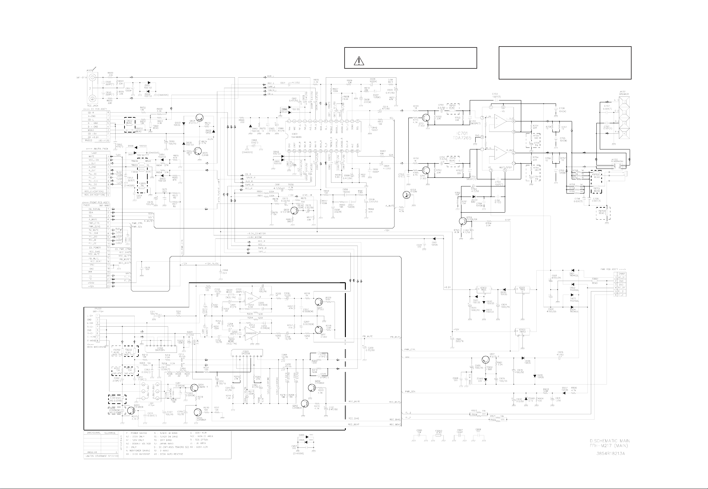
❏ SCHEMATIC DIAGRAMS
• MAIN SCHEMATIC DIAGRAM
2-27 2-28
NOTE:
1. Shaded(
■) parts are critical for safety.Replace
only with specified part number.
2. Voltages are DC-measured with a digital
voltmefer during Play mode.
NOTE: Warning
Parts that are shaded are critical With
respecttoriskoffireorelectricalshock.
Page 34

2-29 2-30
• FRONT SCHEMATIC DIAGRAM
NOTE:
1. Shaded(■) parts are critical for safety.Replace
only with specified part number.
2. Voltages are DC-measured with a digital
voltmefer during Play mode.
NOTE: Warning
Parts that are shaded are critical With
respect to risk of fire or electrical shock.
Page 35

2-31 2-32
❏ WIRING DIAGRAM
Page 36

2-33 2-34
❏ PRINTED CIRCUIT DIAGRAMS
•MAINP.C.BOARD
Page 37

2-35 2-36
• FRONT/POWER P.C. BOARD (COMPONENT SIDE)
Page 38

2-37 2-38
• CDP P.C. BOARD (SOLDER SIDE)
Page 39

2-39 2-40
• CDP P.C. BOARD (COMPONENT SIDE)
Page 40

3-1 3-2
SECTION 3. EXPLODED VIEWS
❏ CABINET AND MAIN FRAME SECTION
301
290
454
454
283
351
264
305
451
302
304
A47
303
454
458
259
A41
A00
458
A26
265
306
250
260
454
284
285
308
286
458
278
279
454
A43
452
310
309
A46
452
262
266
353
258
263
287
NOTE) Refer to “SECTION 5 REPLACEMENT
PARTS LIST” in order to look for the
part number of each part.
Page 41

• TAPE DECK MECHANISM: SINGLE AUTO REVERSE DECK
400
011
503
401
401
009
010
501
502
507
508
013
406
409
410
036
032
038
034
035
039
029
040
031
028
027
026
014
015
403
504
024
025
023
405
A01
402
022
016
017
018
019
020
021
505
007
008
003
004
005
002
404
400
400
506
037
006
3-3 3-4
LOCA. NO PART NO. DESCRIPTION SPECIFICATION
A00 6720AF0002E DECK,AUDIO CRM4212 TOKYO PIGEON L-SINGLE
A01 6768R-UP03A DECK MECHANISM PARTS 50-093-4941 PIGEON PWB ASSY UN
002 6768R-BP03A DECK MECHANISM PARTS 02-083-4252 PIGEON BELT/FELT C
003 6768R-PP03A DECK MECHANISM PARTS 33-160-4309 PIGEON PRESS CASSE
006 6768R-QP03A DECK MECHANISM PARTS 50-093-4891 PIGEON MOTOR(ASSY)
007 6768R-GP03B DECK MECHANISM PARTS 50-222-4578 PIGEON GEAR IDLER
008 6768R-SP01F DECK MECHANISM PARTS 01-082-4598 PIGEON SPRING CWL4
009 6768R-MP01C DECK MECHANISM PARTS 50-219-4014 PIGEON MOLD CWL44
011 6768R-SP01A DECK MECHANISM PARTS 01-081-4601 PIGEON SPRING CWL4
013 6768R-SP03A DECK MECHANISM PARTS 01-082-4686 PIGEON SPRING CRM4
015 6768R-AP01A DECK MECHANISM PARTS 50-268-3016 PIGEON ARM CWL44
016 6768R-GP01H DECK MECHANISM PARTS 50-093-4503 PIGEON GEAR CRL442
017 6768R-AP01C DECK MECHANISM PARTS 50-239-4072 PIGEON ARM CWL44
018 6768R-GP01J DECK MECHANISM PARTS 50-222-4428 PIGEON GEAR CRL442
019 6768R-SP01P DECK MECHANISM PARTS 01-081-4678 PIGEON SPRING CRL4
020 6768R-BP01C DECK MECHANISM PARTS 02-083-4188 PIGEON BELT/FELT C
021 6768R-LP01C DECK MECHANISM PARTS 50-223-4429 PIGEON PULLEY/FLYW
022 6768R-VP03A DECK MECHANISM PARTS 50-093-4748 PIGEON SOLENOID AS
023 6768R-GP03A DECK MECHANISM PARTS 50-093-4810 PIGEON GEAR ASSY C
025 6768R-JP03B DECK MECHANISM PARTS 50-093-31009 PIGEON PULLEY/FLY
026 6768R-SP01D DECK MECHANISM PARTS 01-080-4609 PIGEON SPRING CWL4
027 6768R-DP01A DECK MECHANISM PARTS 50-259-3342 PIGEON LEVER CWL44
028 6768R-RP01A DECK MECHANISM PARTS 22-027-41054 PIGEON ROLLER CWL
029 6768R-MP01A DECK MECHANISM PARTS 50-219-4033 PIGEON MOLD CWL44
031 6768R-SP04A DECK MECHANISM PARTS 01-082-4731 PIGEON SPRING
032 6768R-EP04A DECK MECHANISM PARTS 50-093-41007 PIGEON HEAD ASSY
035 6768R-PP04A DECK MECHANISM PARTS 50-119-4915 PIGEON PRESS
036 6768R-SP04B DECK MECHANISM PARTS 01-081-4730 PIGEON SPRING
037 6768R-JP03A DECK MECHANISM PARTS 50-093-4674 PIGEON PULLEY/FLYW
038 6768R-MP01D DECK MECHANISM PARTS 50-219-4034 PIGEON MOLD CWL44
039 6768R-MP02A DECK MECHANISM PARTS 50-219-3900 PIGEON MOLD
040 6768R-SP01M DECK MECHANISM PARTS 01-080-4607 PIGEON SPRING CWL4
401 6768R-CP01B DECK MECHANISM PARTS GSE20A2005 PIGEON SCREW CWL44
402 6768R-CP01A DECK MECHANISM PARTS GSE10A2003 PIGEON SCREW CWL44
403 6768R-CP01D DECK MECHANISM PARTS GSL10A1704 PIGEON SCREW CWL44
406 6768R-CP01G DECK MECHANISM PARTS GSE20A2004 PIGEON SCREW CWL44
409 6768R-CP02A DECK MECHANISM PARTS GSD10A2016 PIGEON SCREW
501 6768R-WP03A DECK MECHANISM PARTS GWN19S035040 PIGEON WASHER CRM
502 6768R-WP03B DECK MECHANISM PARTS 03-000-4532 PIGEON WASHER CRM4
504 6768R-WP01D DECK MECHANISM PARTS GWP21X045020 PIGEON WASHER CWL
505 6768R-WP01E DECK MECHANISM PARTS GWP12X030040S PIGEON WASHER CW
506 6768R-WP01H DECK MECHANISM PARTS GWP23X040020 PIGEON WASHER CWL
507 6768R-WP01F DECK MECHANISM PARTS GWN21X040040 PIGEON WASHER CWL
Page 42

- 4-1 -
SECTION 4. SPEAKER SECTION
❏ MODEL: FE-M217E
850
851
852
854
853
856
857
855
Page 43

-4-2-
 Loading...