

LG FB162-A0U, FBS162V Service Manual
MODEL : FB162-A0U , FBS162V
SERVICE MANUAL
MODEL : FB162-A0U , FBS162V
CAUTION
BEFORE SERVICING THE UNIT, READ THE “SERVICING PRECAUTIONS”
IN THIS MANUAL.
MINI HOME THEATER
SERVICE MANUAL
Website http://biz.lgservice.com
Internal Use Only
SEPTEMBER, 2007
P/NO : AFN35036931
[CONTENTS]
SECTION 1 SUMMARY
• SERVICING PRECAUTIONS ................................................................................................... 1-2
• ESD PRECAUTIONS ............................................................................................................... 1-3
• SPECIFICATIONS ......................................................................................................................1-5
SECTION 2 EXPLODED VIEWS
1. CABINET AND MAIN FRAME SECTION ................................................................................ 2-1
2. DECK MECHANISM SECTION (DP-10A) ............................................................................... 2-3
3. SPEAKER SECTION .............................................................................................................. 2-5
4. PACKING ACCESSORY SECTION......................................................................................... 2-6
SECTION 3 INTERNAL BLOCK DIAGRAM OF IC’s ...............................................3-1
SECTION 4 ELECTRICAL TROUBLESHOOTING GUIDE OF ADUIO PART .........4-1
SECTION 5 ELECTRICAL TROUBLESHOOTING GUIDE OF DVD PART .............5-1
SECTION 6 BLOCK DIAGRAM ................................................................................6-1
SECTION 7 CIRCUIT DIAGRAM & VOLTAGE CHART ...........................................7-1
SECTION 8 PRINTED CIRCUIT DIAGRAMS ...........................................................8-1
SECTION 9 REPLACEMENT PARTS LIST ..............................................................9-1
Copyright © 2007 LG Electronics. Inc. All right reserved.
Only for training and service purposes
LGE Internal Use Only
1-2
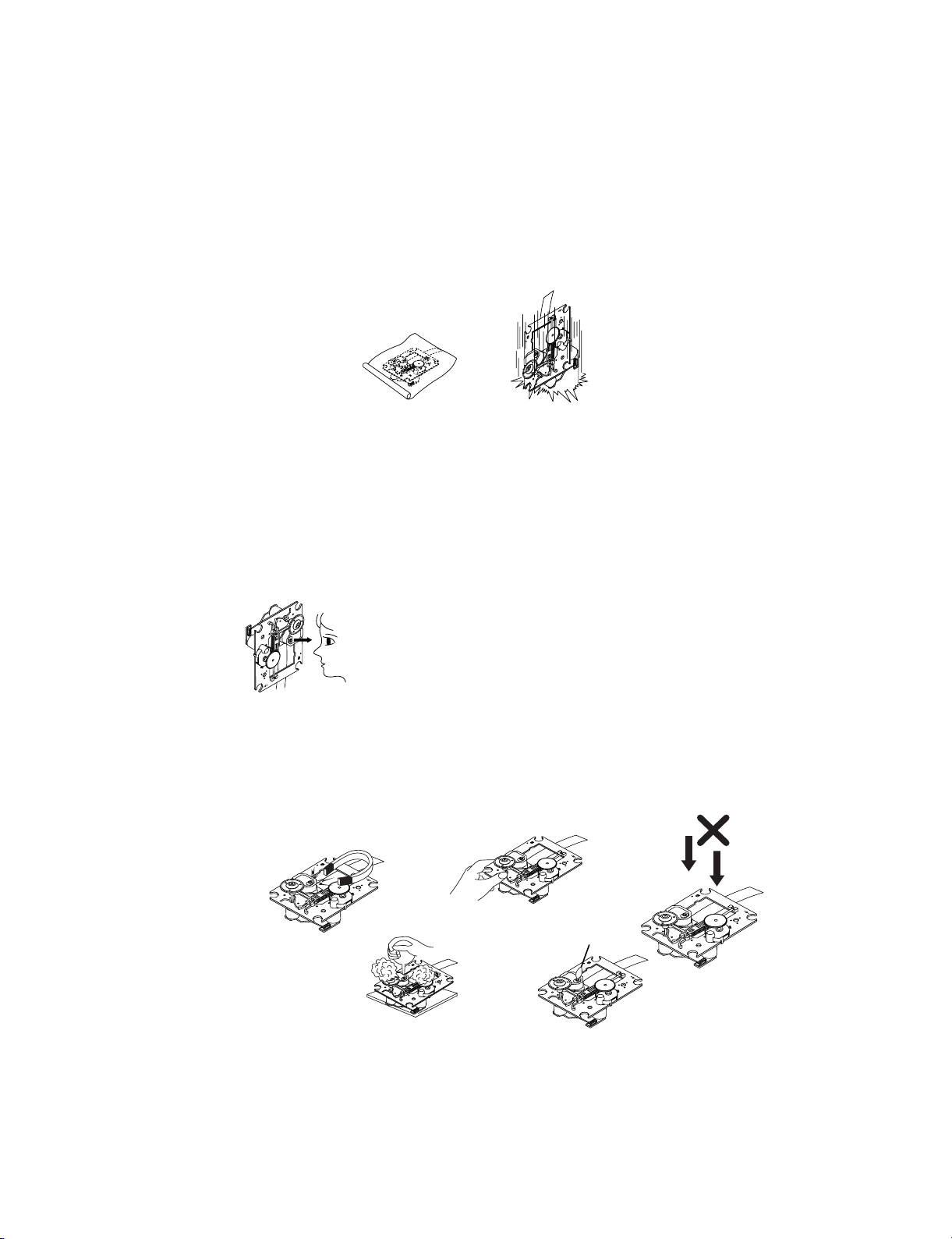
NOTES REGARDING HANDLING OF THE PICK-UP
1. Notes for transport and storage
1) The pick-up should always be left in its conductive bag until immediately prior to use.
2) The pick-up should never be subjected to external pressure or impact.
2. Repair notes
1) The pick-up incorporates a strong magnet, and so should never be brought close to magnetic materials.
2) The pick-up should always be handled correctly and carefully, taking care to avoid external pressure and
impact. If it is subjected to strong pressure or impact, the result may be an operational malfunction and/or
damage to the printed-circuit board.
3) Each and every pick-up is already individually adjusted to a high degree of precision, and for that reason
the adjustment point and installation screws should absolutely never be touched.
4) Laser beams may damage the eyes!
Absolutely never permit laser beams to enter the eyes!
Also NEVER switch ON the power to the laser output part (lens, etc.) of the pick-up if it is damaged.
5) Cleaning the lens surface
If there is dust on the lens surface, the dust should be cleaned away by using an air bush (such as used
for camera lens). The lens is held by a delicate spring. When cleaning the lens surface, therefore, a cotton swab should be used, taking care not to distort this.
6) Never attempt to disassemble the pick-up.
Spring by excess pressure. If the lens is extremely dirty, apply isopropyl alcohol to the cotton swab.
(Do not use any other liquid cleaners, because they will damage the lens.) Take care not to use too much
of this alcohol on the swab, and do not allow the alcohol to get inside the pick-up.
Storage in conductive bag
Drop impact
NEVER look directly at the laser beam, and don’t let
contact fingers or other exposed skin.
Magnet
How to hold the pick-up
Conductive Sheet
Cotton swab
Pressure
Pressure
SECTION 1 SUMMARY
SERVICING PRECAUTIONS
Copyright © 2007 LG Electronics. Inc. All right reserved.
Only for training and service purposes
LGE Internal Use Only
1-3
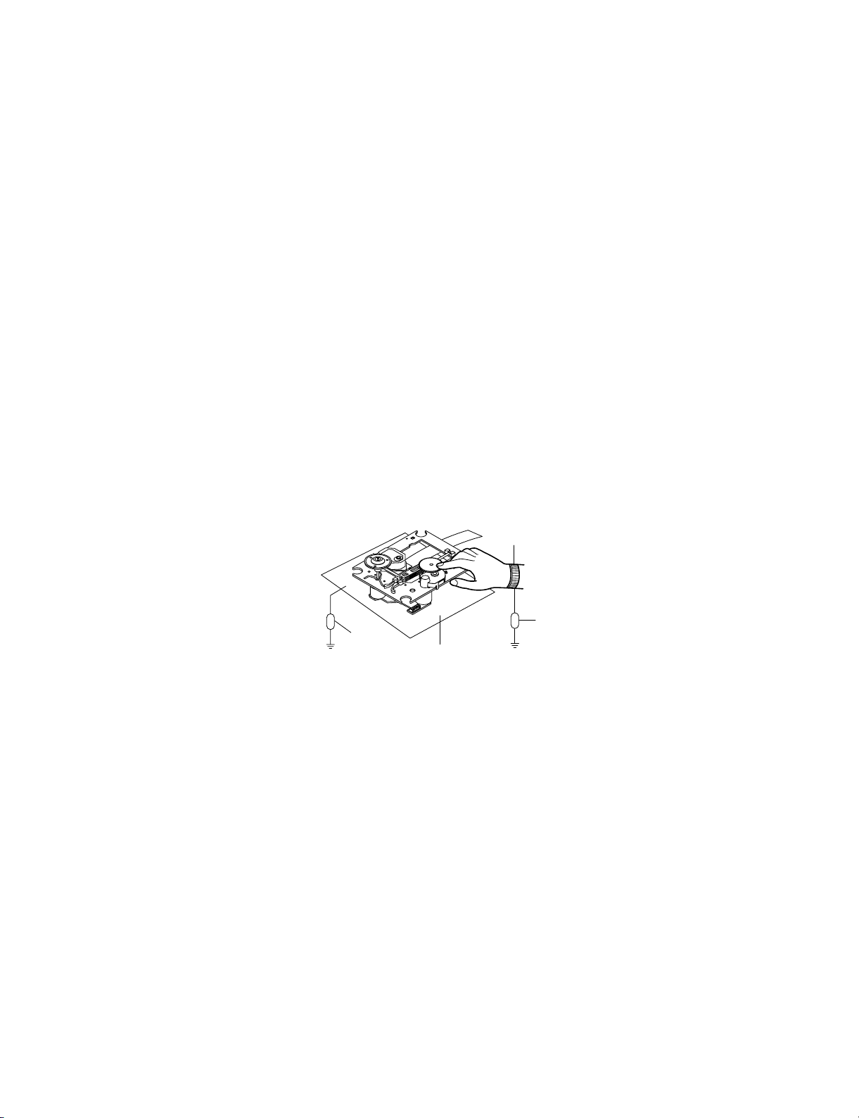
NOTES REGARDING COMPACT DISC PLAYER REPAIRS
1. Preparations
1) Compact disc players incorporate a great many ICs as well as the pick-up (laser diode). These components
are sensitive to, and easily affected by, static electricity. If such static electricity is high voltage, components
can be damaged, and for that reason components should be handled with care.
2) The pick-up is composed of many optical components and other high-precision components. Care must be
taken, therefore, to avoid repair or storage where the temperature of humidity is high, where strong magnetism is present, or where there is excessive dust.
2. Notes for repair
1) Before replacing a component part, first disconnect the power supply lead wire from the unit
2) All equipment, measuring instruments and tools must be grounded.
3) The workbench should be covered with a conductive sheet and grounded.
When removing the laser pick-up from its conductive bag, do not place the pick-up on the bag. (This is
because there is the possibility of damage by static electricity.)
4) To prevent AC leakage, the metal part of the soldering iron should be grounded.
5) Workers should be grounded by an armband (1M Ω)
6) Care should be taken not to permit the laser pick-up to come in contact with clothing, in order to prevent
static electricity changes in the clothing to escape from the armband.
7) The laser beam from the pick-up should NEVER be directly facing the eyes or bare skin.
Resistor
(1 Mohm)
Conductive
Sheet
Resistor
(1 Mohm)
Armband
Copyright © 2007 LG Electronics. Inc. All right reserved.
Only for training and service purposes
LGE Internal Use Only
1-4
ESD PRECAUTIONS
Electrostatically Sensitive Devices (ESD)
Some semiconductor (solid state) devices can be damaged easily by static electricity. Such components
commonly are called Electrostatically Sensitive Devices (ESD). Examples of typical ESD devices are integrated
circuits and some field-effect transistors and semiconductor chip components. The following techniques should
be used to help reduce the incidence of component damage caused by static electricity.
1. Immediately before handling any semiconductor component or semiconductor-equipped assembly, drain off
any electrostatic charge on your body by touching a known earth ground. Alternatively, obtain and wear a
commercially available discharging wrist strap device, which should be removed for potential shock reasons
prior to applying power to the unit under test.
2. After removing an electrical assembly equipped with ESD devices, place the assembly on a conductive surface
such as aluminum foil, to prevent electrostatic charge buildup or exposure of the assembly.
3. Use only a grounded-tip soldering iron to solder or unsolder ESD devices.
4. Use only an anti-static solder removal device. Some solder removal devices not classified as "anti-static" can
generate electrical charges sufficient to damage ESD devices.
5. Do not use freon-propelled chemicals. These can generate electrical charges sufficient to damage ESD
devices.
6. Do not remove a replacement ESD device from its protective package until immediately before you are
ready to install it. (Most replacement ESD devices are packaged with leads electrically shorted together by
conductive foam, aluminum foil or comparable conductive materials).
7. Immediately before removing the protective material from the leads of a replacement ESD device, touch the
protective material to the chassis or circuit assembly into which the device will by installed.
CAUTION : BE SURE NO POWER IS APPLIED TO THE CHASSIS OR CIRCUIT, AND OBSERVE ALL OTHER
SAFETY PRECAUTIONS.
8. Minimize bodily motions when handing unpackaged replacement ESD devices. (Otherwise harmless motion
such as the brushing together of your clothes fabric or the lifting of your foot from a carpeted floor can generate static electricity sufficient to damage an ESD device).
CAUTION. GRAPHIC SYMBOLS
THE LIGHTNING FLASH WITH APROWHEAD SYMBOL. WITHIN AN EQUILATERAL TRIANGLE, IS
INTENDED TO ALERT THE SERVICE PERSONNEL TO THE PRESENCE OF UNINSULATED
“DANGEROUS VOLTAGE” THAT MAY BE OF SUFFICIENT MAGNITUDE TO CONSTITUTE A RISK OF
ELECTRIC SHOCK.
THE EXCLAMATION POINT WITHIN AN EQUILATERAL TRIANGLE IS INTENDED TO ALERT THE
SERVICE PERSONNEL TO THE PRESENCE OF IMPORTANT SAFETY INFORMATION IN SERVICE
LITERATURE.
Copyright © 2007 LG Electronics. Inc. All right reserved.
Only for training and service purposes
LGE Internal Use Only

1-5
GENERAL
Power supply Refer to main label
Power consumption Refer to main label
Net Weight 3.31 kg
External dimensions (W x H x D) 170 x 253 x 265 mm
Operating conditions Temperature: 5°C to 35°C, Operation status: Horizontal
Operating humidity 5% to 85%
CD/DVD
Laser Semiconductor laser, wavelength 650 nm
Signal system NTSC 525/60, PAL 652/50
Frequency response (audio) 40 Hz to 2 kHz
Signal-to-noise ratio (audio) More than 75 dB (1 kHz, NOP -3 dB, 20 kHz LPF/A-Filter)
Dynamic range (audio) More than 75 dB
Harmonic distortion (audio) 0.5 % (1 kHz, at 1W position) (20 kHz LPF)
VIDEO
Video output 1.0 V (p-p), 75 Ω, negative sync./ RCA jack x 1
COMPONENT VIDEO OUT (Y) 1.0 V (p-p), 75 ohms, negative sync, RCA jack x 1
(Pb)/(Pr) 0.7 V (p-p), 75 ohms, RCA jack x 1
Tuner
FM
Tuning Range 87.5 - 108.0 MHz or 65.0 - 74.0 MHz, 87.5 - 108.0 MHz
Intermediate Frequency 10.7 MHz
Signal-to Noise Ratio 60/55 dB (Mono)
Frequency Response 50 - 10,000 Hz
AM [ MW ]
Tuning Range 522 - 1,620 kHz or 520 - 1,720 kHz
Intermediate Frequency 450 kHz
AMPLIFIER
Stereo mode 80 W + 80 W
Output Power 80 W + 80 W
T.H.D 0.5 %
Frequency Response 40 - 20000 Hz
Signal-to-noise ratio 75 dB
SPEAKERS
Type 3 Way 3 Speaker
Impedance 4 Ω
Frequency Response 70 - 20,000 Hz
Sound Pressure Level 83 dB/W (1m)
Rated Input Power 80 W
Max. Input Power 160 W
Net Dimensions (W x H x D) 128 x 295 x 240 mm
Net Weight 4.1kg
SPECIFICATIONS
Copyright © 2007 LG Electronics. Inc. All right reserved.
Only for training and service purposes
LGE Internal Use Only
Copyright © 2007 LG Electronics. Inc. All right reserved.
Only for training and service purposes
LGE Internal Use Only
2-1 2-2
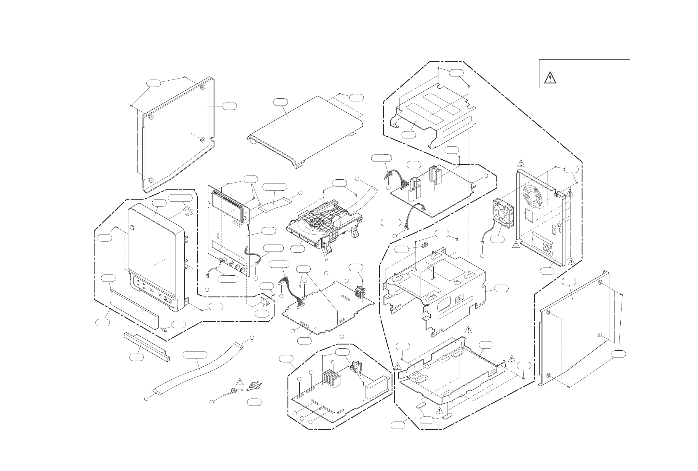
SECTION 2 EXPLODED VIEWS
1. CABINET AND MAIN FRAME SECTION
Copyright © 2007 LG Electronics. Inc. All right reserved.
Only for training and service purposes
LGE Internal Use Only
463
252
463
250
CABLE1
262
261
NOTES) THE EXCLAMATION POINT WITHIN AN
463
463
EQUILATERAL TRIANGLE IS INTENDED
TO ALERT THE SERVICE PERSONNEL
TO THE PRESENCE OF IMPORTANT
SAFETY INFORMATION IN SERVICE
LITERATURE.
264
468
P9701
463
CABLE3
A47
463
G
F
J
L
463
P9702
A50
K
CN303
P5701
CN302
A
C
463
A26
463
A
I
E
463
F
276
463
267
M
259
263
265
A43
257
B
253
CABLE2
463
L
H
300
275
A46
B
A52
J
I
H
K
G
E
463
463
M
273
463
63
4
274
A44
2-3 2-4
2. DECK MECHANISM SECTION (DP-10A)
Copyright © 2007 LG Electronics. Inc. All right reserved.
Only for training and service purposes
LGE Internal Use Only
A26
012
019
013
017
439
014
435
015
018
015B
015A
016
012
440
030
001
002
003
432
A01
A02
020
012A
010
026
A03
036
025
439
024
431
435
012A
021
430
2-5
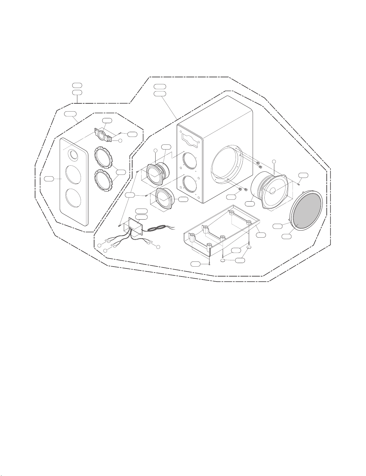
3. SPEAKER SECTION(FBS162V)
Copyright © 2007 LG Electronics. Inc. All right reserved.
Only for training and service purposes
LGE Internal Use Only
A80
A80A
:LEFT SPK ASS'Y
A81
:RIGHT SPK ASS'Y
851
853
B
A80L
A80R
A
:LEFT CABINET ASS'Y
:RIGHT CABINET ASS'Y
855
C
850
852
854
857L
857R
A
C
B
856
854
858
859
861
863
854
864
860
862
2-6
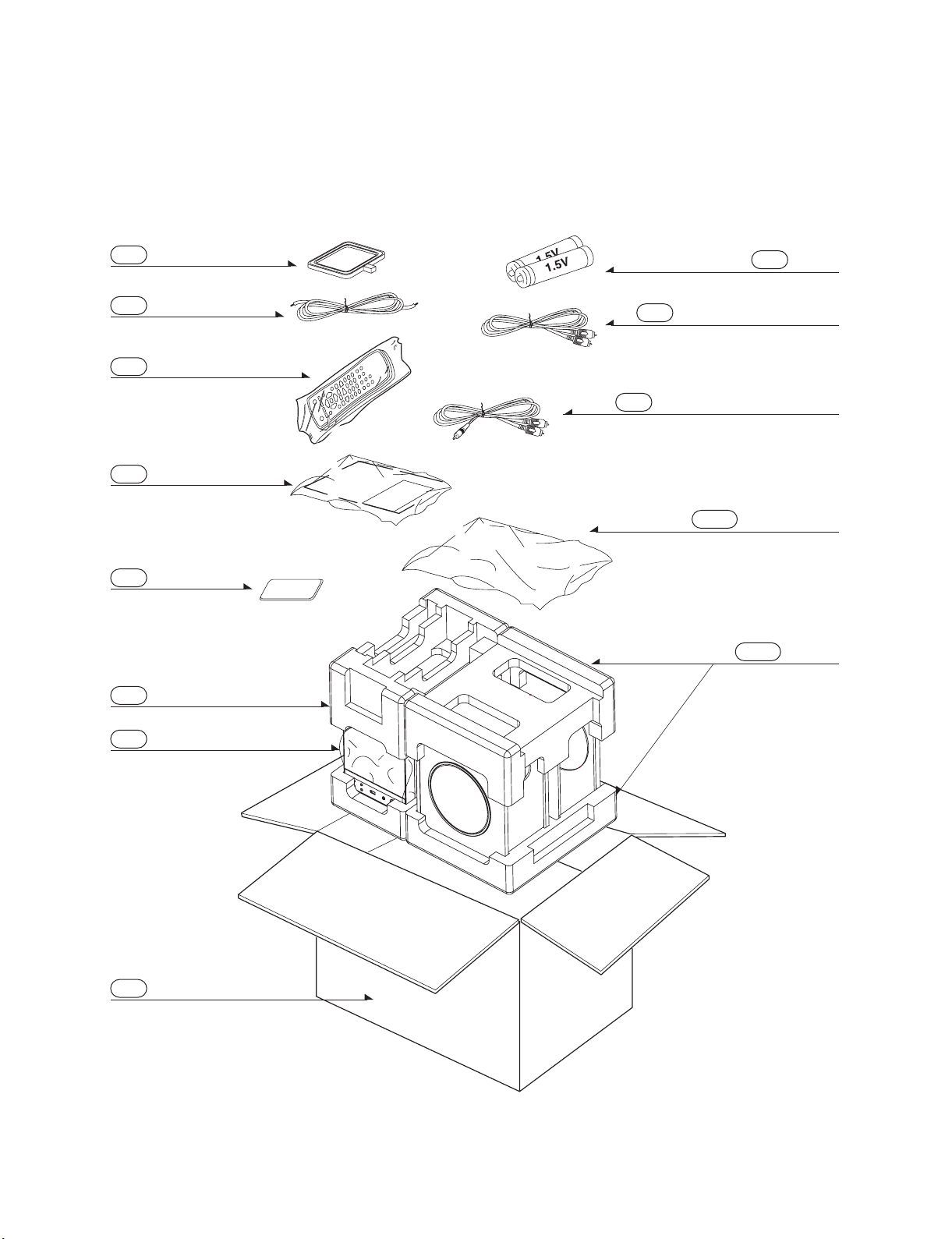
4. PACKING ACCESSORY SECTION
Copyright © 2007 LG Electronics. Inc. All right reserved.
Only for training and service purposes
LGE Internal Use Only
Antenna Loop
824
808
Battery
Antenna825
Remote control900
Instruction Ass'y801
Clear Sheet805
Packing803
Bag804
Plug Ass'y, 1Way(BLACK)
811
Plug Ass'y, 1Way(Red-White)813
804A
Accessory Bag
803A
Packing
Box802
3-1
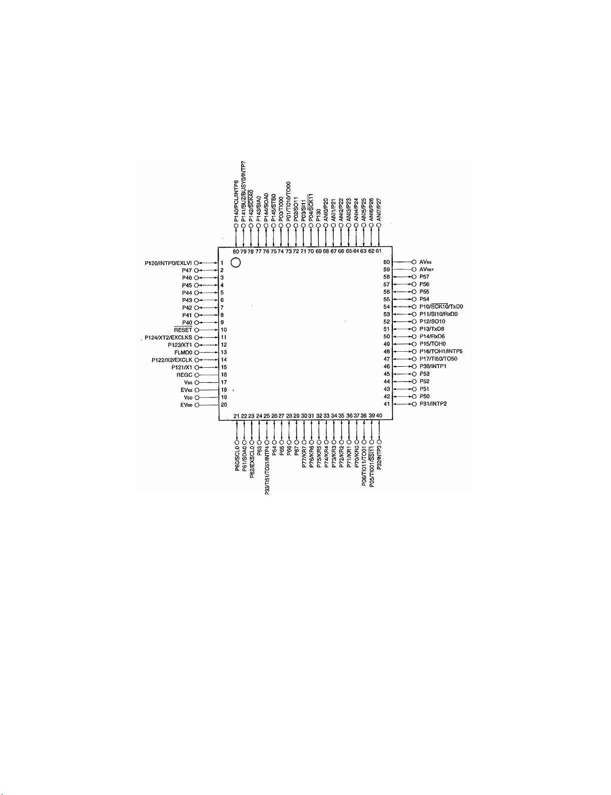
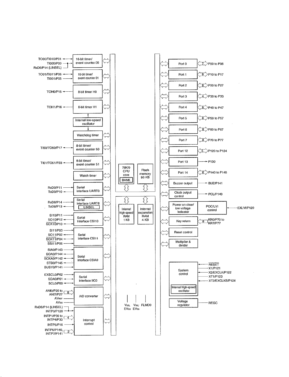
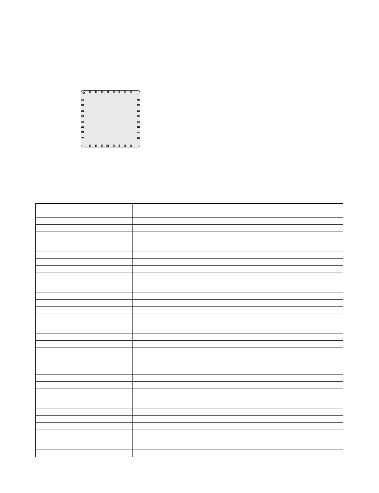
SECTION 3 INTERNAL BLOCK DIAGRAM OF IC’S
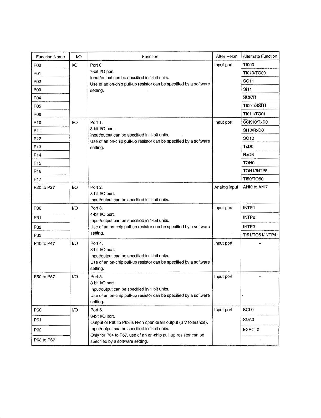
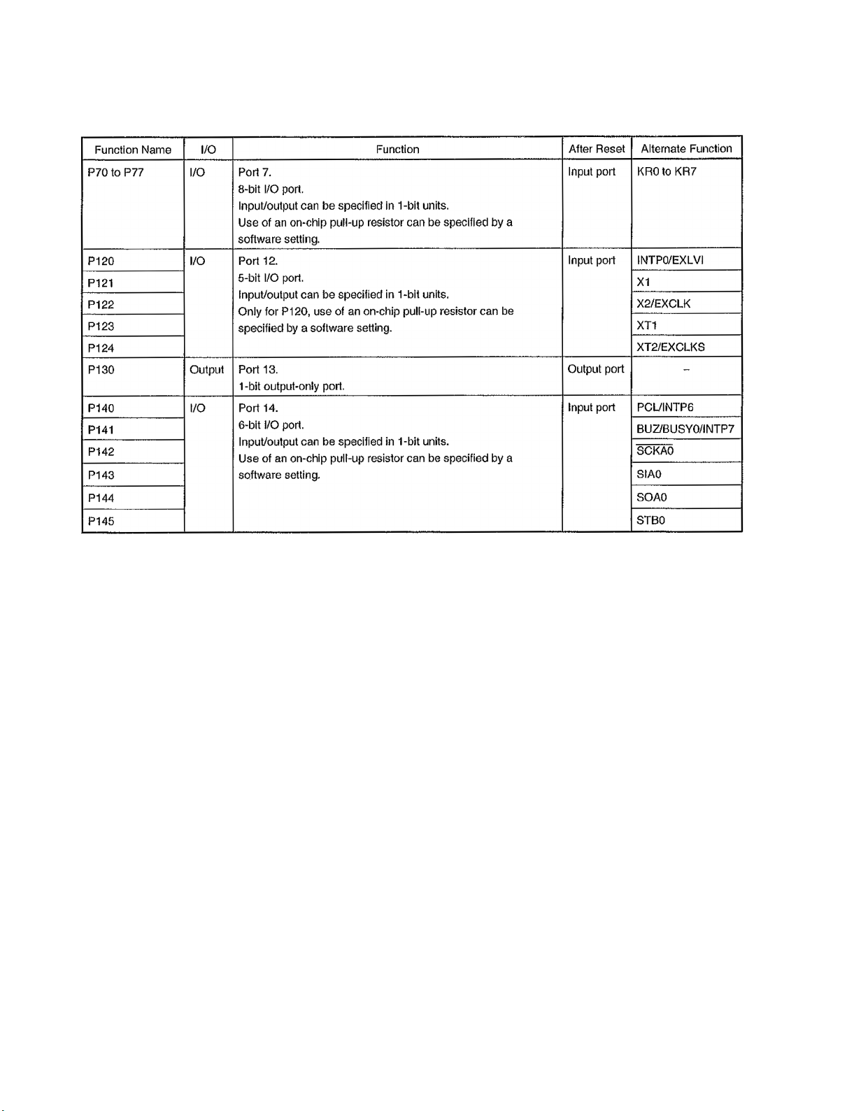
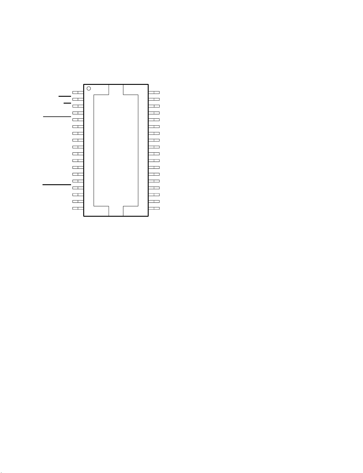
1. µPD78F0546R(R)
• PIN CONFIGURATION(TOP VIEW)
Copyright © 2007 LG Electronics. Inc. All right reserved.
Only for training and service purposes
LGE Internal Use Only
3-2
• BLOCK DIAGRAM
Copyright © 2007 LG Electronics. Inc. All right reserved.
Only for training and service purposes
LGE Internal Use Only
3-3
• PIN FUNCTION
Copyright © 2007 LG Electronics. Inc. All right reserved.
Only for training and service purposes
LGE Internal Use Only
3-4
Copyright © 2007 LG Electronics. Inc. All right reserved.
Only for training and service purposes
LGE Internal Use Only
3-5
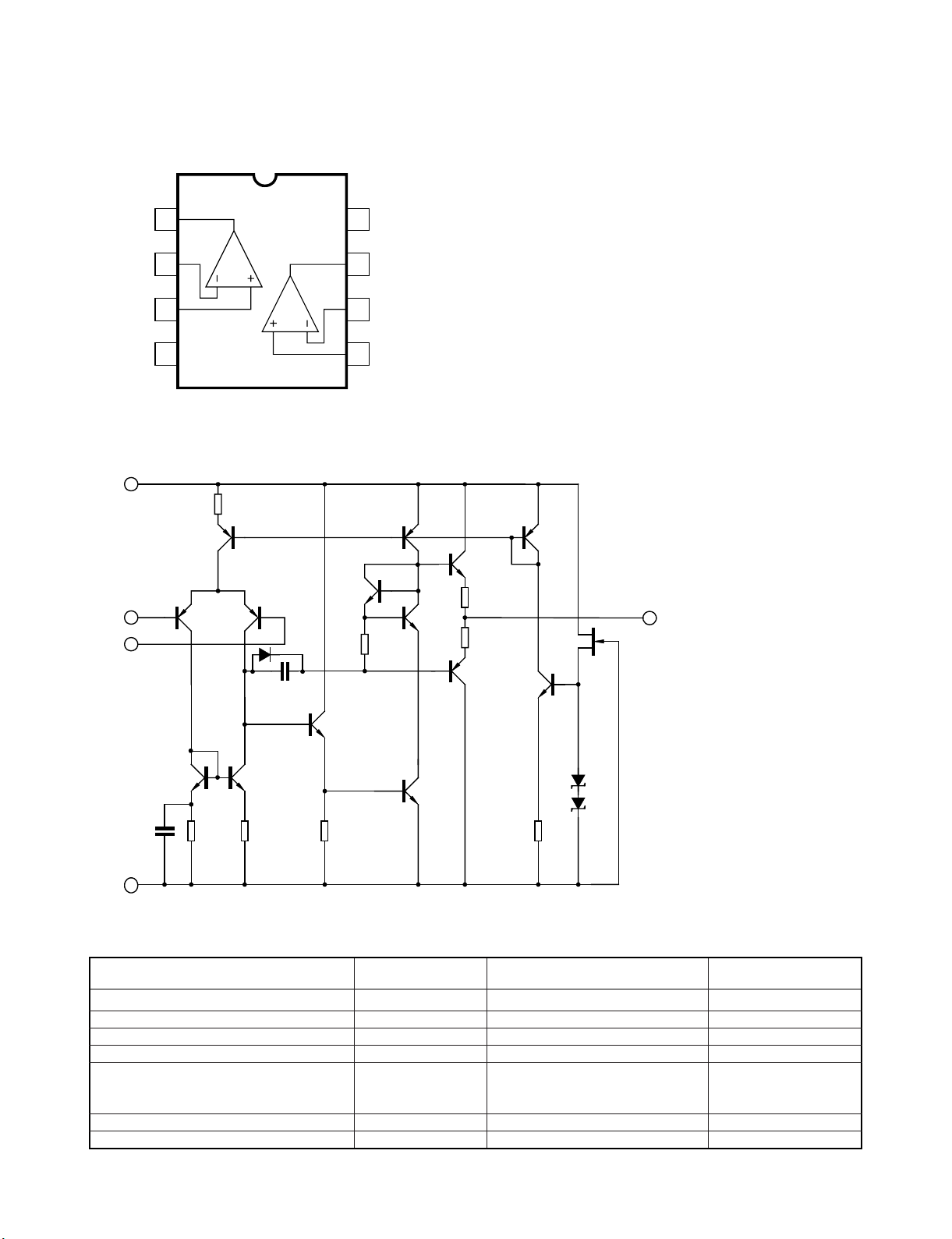
2. MC4580
• PIN CONFIGURATION
• TEST CIRCUIT
• ABSOLUTE MAXIMUM RATINGS (TA=25°C)
SYMBOL RATINGS UNITPARAMETER
Supply Voltage V+/V- ±18 V
Input Voltage V
IC ±5 V
Differential Input Voltage V
ID ±30 V
Output Current I
o ±50 mA
Power Dissipation P
D 300 (SOP-8) mW
800 (DIP-8)
250(TSSOP-8)
Operating Temperature Range Topr -40 to+85 °C
Storage Temperature Range Tstg -40 to +125 °C
Copyright © 2007 LG Electronics. Inc. All right reserved.
Only for training and service purposes
LGE Internal Use Only
1
IN1(-)
Vcc-
2
3
4
Vcc+
IN(-)
IN(+)
Vcc+OUT1
8
OUT2
7
6
IN2(-)IN1(+)
5
IN2(+)
OUTP
UT
Vcc-
3-6
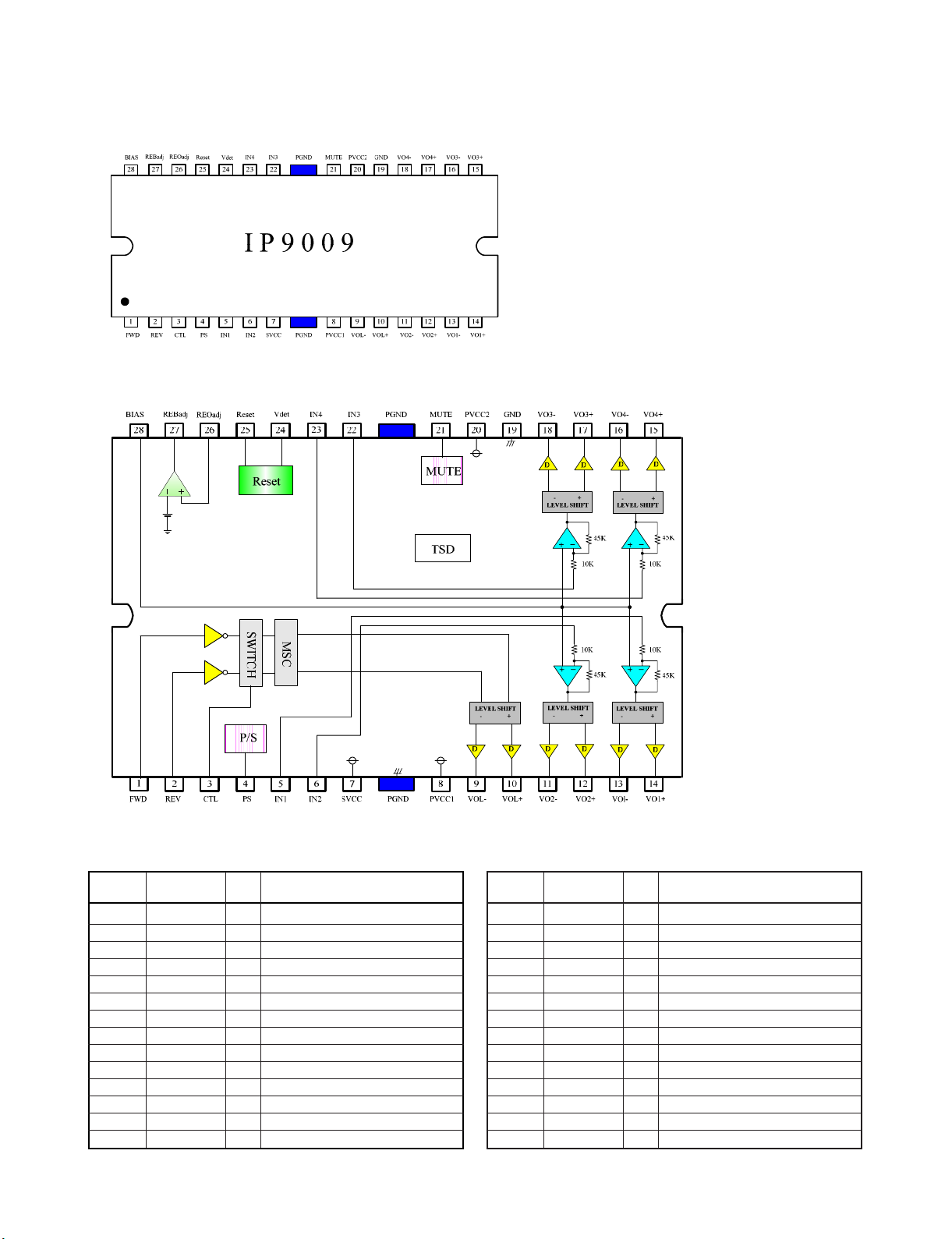
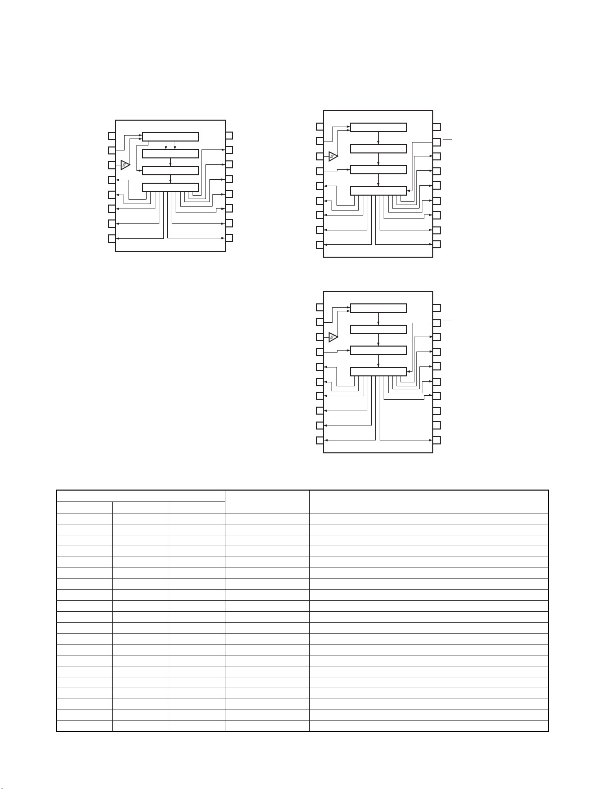
3. IP9009
• PIN CONFIGURATION
• BLOCK DIAGRAM
• PIN DESCRIPTION
No SYMBOL I/O SYMBOL
1 FWD I Loading motor forward input
2 REV I Loading motor reverse input
3 CTL I Loading motor speed control
4 PS I Power save
5 IN1 I CH1 input
6 IN2 I CH2 input
7 SVCC - Signal power supply
8 PVCC1 - Power supply 1
9 VOL- O Loading driver output(-)
10 VOL+ O Loading driver output(+)
11 VO2- O CH2 driver output(-)
12 VO2+ O CH2 driver output(+)
13 VO1- O CH1 driver output(-)
14 VO1+ O CH1 driver output(+)
No SYMBOL I/O SYMBOL
15 VO4+ O CH4 driver output(+)
16 VO4- O CH4 driver output(-)
17 VO3+ O CH3 driver output(+)
18 VO3- O CH3 driver output(-)
19 GND - Ground
20 PVCC2 - Power supply 2
21 MUTE I Mute
22 IN3 I CH3 input
23 IN4 I CH4 input
24 Vdet I Reset controller input
25 Reset O Reset controller output
26 REOadj O Adjustable regulator feedback
27 REBadj O Adjustable regulator control
28 BIAS I Bias
Copyright © 2007 LG Electronics. Inc. All right reserved.
Only for training and service purposes
LGE Internal Use Only
3-7
4. CY8C21434
• PIN CONFIGURATION
• PIN DESCRIPTION
SYMBOL DescriptionPin No.
Type
Digital Analog
1 IO I, M P0[1] Analog column mux input, integrating input.
2 IO M P2[7]
3 IO M P2[5]
4 IO M P2[3]
5 IO M P2[1]
6 IO M P3[3] In CY8C21434 part.
6 Power SMP Switch Mode Pump (SMP) connection to required external
components in CY8C21634 part.
7 IO M P3[1] In CY8C21434 part.
7 Power Vss Ground connection in CY8C21634 part.
8 IO M P1[7] I2C Serial Clock (SCL).
9 IO M P1[5] I2C Serial Data (SDA).
10 IO M P1[3]
11 IO M P1[1] I2C Serial Clock (SCL), ISSP-SCLK*.
12 Power Vss Ground connection.
13 IO M P1[0] I2C Serial Data (SDA), ISSP-SDATA*.
14 IO M P1[2]
15 IO M P1[4] Optional External Clock Input (EXTCLK).
16 IO M P1[6]
17 Input XRES Active high external reset with internal pull down.
18 IO M P3[0]
19 IO M P3[2]
20 IO M P2[0]
21 IO M P2[2]
22 IO M P2[4]
23 IO M P2[6]
24 IO I, M P0[0] Analog column mux input.
25 IO I, M P0[2] Analog column mux input.
26 IO I, M P0[4] Analog column mux input.
27 IO I, M P0[6] Analog column mux input.
28 Power Vdd Supply voltage.
29 IO I, M P0[7] Analog column mux input.
30 IO I, M P0[5] Analog column mux input.
31 IO I, M P0[3] Analog column mux input, integrating input.
32 Power Vss Ground connection.
Copyright © 2007 LG Electronics. Inc. All right reserved.
Only for training and service purposes
LGE Internal Use Only
Vss
P0[3], A, I, M
A, I, M, P0[1]
M, P2[7 ]
M, P2[5 ]
M, P2[3 ]
M, P2[1 ]
M, P3[3 ]
M, P3[1 ]
M, I2 C S CL , P1 [ 7 ]
32313029282726
1
2
3
4
5
(Top View )
6
7
8
9
10111213141516
M, P1[3]
P0[5], A, I, M
QFN
Vss
P0[7], A, I, M
Vdd
P0[6], A, I, M
P0[4], A, I, M
P0[2], A, I, M
25
P0[0 ], A , I, M
24
P2[6 ], M
23
22
P2[4 ], M
P2[2 ], M
21
P2[0 ], M
20
P3[2 ], M
19
P3[0 ], M
18
XRES
17
M, P1[2]
M, P1[6]
M, I2C SCL, P1[1]
M, I2C SDA, P1[5]
M, EXTCLK, P1[4]
M, I2C SDA, P1[0]
3-8
5. BU2090
• PIN CONFIGURATION
• PIN DESCRIPTION
PIN NAME FUNCTION
TYPE
BU2092/F
BU2090/F/FS
BU2092/FV
1 1 1 DATA GN D
2 2 2 CLOCK Serial data input
3 3 3 LCK Data shift clock input
— 4 4 Q0 Data latch clock input
4 5 5 Q1 Parallel data output
5 6 6 Q2 Parallel data output
6 7 7 Q3 Parallel data output
7 8 8 Q4 Parallel data output
8 9 9 Q5 Parallel data output
9 10 10 Q6 Parallel data output
10 11 11 N.C. Parallel data output
— — 12 N.C. Not connected
— — 13 Q7 Not connected
11 12 14 Q8 Parallel data output
12 13 15 Q9 Parallel data output
13 14 16 Q10 Parallel data output
14 15 17 Q11 Parallel data output
15 16 18 OE Parallel data output
— 17 19 VSS Output Enable
16 18 20 VDD Power supply
Copyright © 2007 LG Electronics. Inc. All right reserved.
Only for training and service purposes
LGE Internal Use Only
BU2090 / F / FS BU2092 / F
16
VSS
DATA
CLOCK
Q0
Q1
Q2
Q3
Q4
1
2
3
4
5
6
7
8
Control circuit
12-bit shift register
Latch
Output buffer
(open drain)
VDD
15
Q11
14
Q10
13
Q9
12
Q8
11
Q7
10
Q6
9
Q5
BU2092FV
VSS
DATA
CLOCK
LCK
Q0
Q1
Q2
Q3
Q4
VSS
DATA
CLOCK
LCK
Q0
Q1
Q2
Q3
Q4
Q5
1
2
3
4
5
6
7
8
9
1
2
3
4
5
6
7
8
9
10
Control circuit
12-bit shift register
1
12-bit storage register
Output buffer
(open drain)
Control circuit
12-bit shift register
12-bit storage register
Output buffer (open drain)
18
V
DD
17
OE
16
Q11
15
Q10
14
Q9
13
Q8
12
Q7
11
Q6
10
Q5
20
V
DD
19
OE
18
Q11
17
Q10
16
Q9
15
Q8
14
Q7
13
N.C.
12
N.C.
11
Q6
3-9
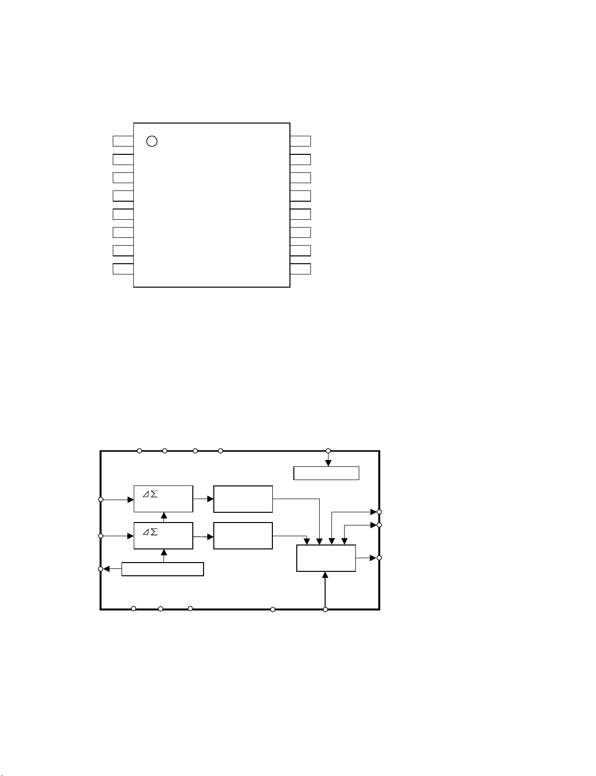
6. AK5358
• PIN CONFIGURATION
• BLOCK DIAGRAM
Copyright © 2007 LG Electronics. Inc. All right reserved.
Only for training and service purposes
LGE Internal Use Only
AINR
AINL
CKS1
VCOM
AGND
VA
VD
DGND
1
2
3
4
5
6
7
8
Top View
16
15
14
13
12
11
10
9
CKS0
CKS2
DIF
PDN
SCLK
MCLK
LRCK
SDTO
AINL
AINR
VCOM
AGNDVA
Modulator
Modulator
Vo
ltage Reference
CKS1
CKS2
CKS0
DGNDVD
Decimation
Decimation
Filter
Filter
PDN
MCLK
Clock Divider
Serial I/O
Interface
DIF
LRCK
SCLK
SDTO
3-10
• PIN DESCRIPTION
No PIN NAME I/O SYMBOL
1 AINR I Rch Analog Input Pin
2 AINL I Lch Analog Input Pin
3 CKS1 I Mode Select 1 Pin
4 VCOM O Common Voltage Output Pin, VA/2
Bias voltage of ADC input.
5 AGND - Analog Ground Pin
6 VA - Analog Power Supply Pin, 4.5 ~ 5.5V
7 VD - Digital Power Supply Pin, 2.7 ~ 3.6V
8 DGND - Digital Ground Pin
9 SDTO O Audio Serial Data Output Pin
“L” Output at Power-down mode.
10 LRCK I/O Output Channel Clock Pin
“L” Output in Master Mode at Power-down mode.
11 MCLK I Master Clock Input Pin
12 SCLK I/O Audio Serial Data Clock Pin
“L” Output in Master Mode at Power-down mode.
13 PDN I Power Down Mode & Reset Pin
“H”: Power up, “L”: Power down & Reset
The AK5358 must be reset once upon power-up.
14 DIF I Audio Interface Format Pin
“H”: 24bit I2S Compatible, “L”: 24bit MSB justified
15 CKS2 I Mode Select 2 Pin
16 CKS0 I Mode Select 0 Pin
Copyright © 2007 LG Electronics. Inc. All right reserved.
Only for training and service purposes
LGE Internal Use Only
3-11
7. HT1000
• PIN CONFIGURATION
Copyright © 2007 LG Electronics. Inc. All right reserved.
Only for training and service purposes
LGE Internal Use Only
DKD PACKAGE
(T
OP VIEW)
GVDD_B
OTW
SD
PWM_A
RESET_AB
PWM_B
OC_ADJ
GND
AGND
VREG
M3
M2
M1
PWM_C
RESET_CD
PWM_D
VDD
GVDD_C
1
2
3
4
5
6
7
8
9
10
11
12
13
14
15
16
17
18
36
35
34
33
32
31
30
29
28
27
26
25
24
23
22
21
20
19
GVDD_A
BST_A
PVDD_A
OUT_A
GND_A
GND_B
OUT_B
PVDD_B
BST_B
BST_C
PVDD_C
OUT_C
GND_C
GND_D
OUT_D
PVDD_D
BST_D
GVDD_D
 Loading...