

Page 1

DLP PROJECTION TV
SERVICE MANUAL
CAUTION
BEFORE SERVICING THE CHASSIS,
READ THE SAFETY PRECAUTIONS IN THIS MANUAL.
CHASSIS : NB-04AA
MODEL : DU-52SZ61D
CANADA : http//biz.lgservice.com
USA : http//www.lgservice.com
: http//lgservice.com/techsup.html
Page 2
- 2 -
SAFETY PRECAUTIONS
Many electrical and mechanical parts in this chassis have special safety-related characteristics. These parts are identified by in
the Schematic Diagram and Replacement Parts List.
It is essential that these special safety parts should be replaced with the same components as recommended in this manual to
prevent X-RADIATION, Shock, Fire, or other Hazards.
Do not modify the original design without permission of manufacturer.
General Guidance
An lsolation Transformer should always be used during
the servicing of a receiver whose chassis is not isolated from
the AC power line. Use a transformer of adequate power rating
as this protects the technician from accidents resulting in
personal injury from electrical shocks.
It will also protect the receiver and it's components from being
damaged by accidental shorts of the circuitary that may be
inadvertently introduced during the service operation.
If any fuse (or Fusible Resistor) in this monitor is blown, replace
it with the specified.
When replacing a high wattage resistor (Oxide Metal Film
Resistor, over 1W), keep the resistor 10mm away from PCB.
Keep wires away from high voltage or high temperature parts.
Due to high vacuum and large surface area of picture tube,
extreme care should be used in handling the Picture Tube.
Do not lift the Picture tube by it's Neck.
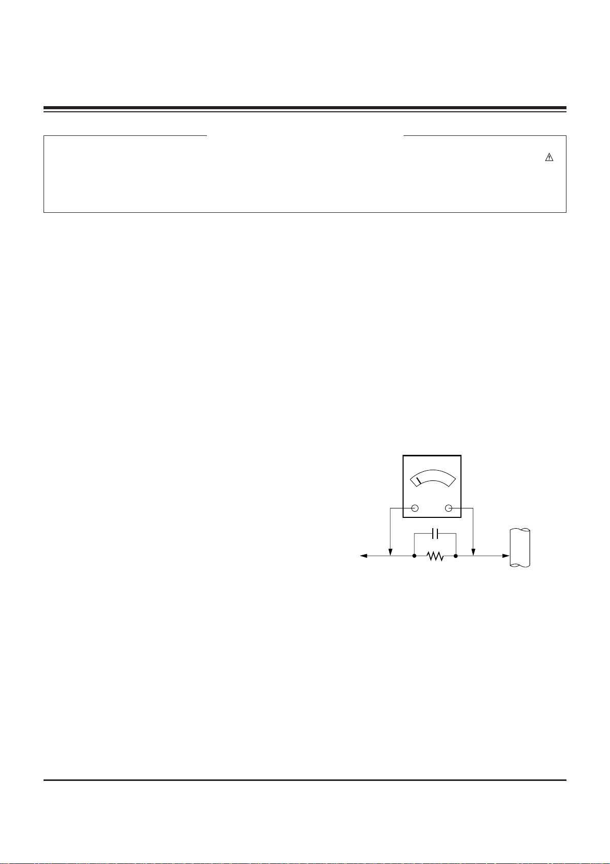
Leakage Current Cold Check(Antenna Cold Check)
With the instrument AC plug removed from AC source,
connect an electrical jumper across the two AC plug prongs.
Place the AC switch in the on positioin, connect one lead of
ohm-meter to the AC plug prongs tied together and touch other
ohm-meter lead in turn to each exposed metallic parts such as
antenna terminals, phone jacks, etc.
If the exposed metallic part has a return path to the chassis, the
measured resistance should be between 1MΩ and 5.2MΩ.
When the exposed metal has no return path to the chassis the
reading must be infinite.
An other abnormality exists that must be corrected before the
receiver is returned to the customer.
Leakage Current Hot Check (See below Figure)
Plug the AC cord directly into the AC outlet.
Do not use a line Isolation Transformer during this check.
Connect 1.5K/10watt resistor in parallel with a 0.15uF capacitor
between a known good earth ground (Water Pipe, Conduit, etc.)
and the exposed metallic parts.
Measure the AC voltage across the resistor using AC
voltmeter with 1000 ohms/volt or more sensitivity.
Reverse plug the AC cord into the AC outlet and repeat AC
voltage measurements for each esposed metallic part. Any
voltage measured must not exceed 0.75 volt RMS which is
corresponds to 0.5mA.
In case any measurement is out of the limits sepcified, there is
possibility of shock hazard and the set must be checked and
repaired before it is returned to the customer.
Leakage Current Hot Check circuit
CANADA: LG Electronics Canada, Inc. 550 Matheson
Boulevard East Mississauga, Ontario L4Z 4G3
USA : LG Customer Interactive Center
P.O.Box 240007, 201 James Record Road Huntsville,
AL 35824
Digital TV Hotline 1-800-243-0000
1.5 Kohm/10W
To Instrument's
exposed
METALLIC PARTS
Good Earth Ground
such as WATER PIPE,
CONDUIT etc.
AC Volt-meter
IMPORTANT SAFETY NOTICE
0.15uF
Page 3

- 3 -
SPECIFICATIONS.................................................................4
DESCRIPTION OF CONTROLS...........................................5
ADJUSTMENT INSTRUCTION.............................................8
PRINTED CIRCUIT BOARDS.............................................21
BLOCK DIAGRAM...............................................................31
EXPLODED VIEW...............................................................32
EXPLODED VIEW PARTS LIST.........................................33
REPLACEMENT PARTS LIST............................................34
SCHEMATIC DIAGRAM..........................................................
TABLE OF CONTENTS
Page 4

- 4 -
• The specifications shown above may be changed without prior notice for quality improvement.
MODELS
AC120V, 60Hz
NTSC-M, ATSC
VHF 2 ~ 13, UHF 14 ~ 69, CATV 1 ~ 135, CADTV 1 ~ 135. DTV 2 ~ 69
75 Ω
Power requirement
Television System
Program Coverage
External Antenna Impedance
DU-52SZ51D / DU-52SZ61D
SPECIFICATIONS
Page 5
- 5 -
Controls
Controls
POWER TV GUIDE VOL CH
ENTER
POWER Button
VOLUME (
FF,GG
) Buttons
Remote Control Sensor
CHANNEL (EE, DD) Buttons
Operation Indicator
Lamp Indicator
Temperature Indicator
ENTER Button
TV GUIDE Button
Off Power Cord is not connected.
Red Power Cord is connected, TV is in standby mode.
Green TV turns on.
Red (flashing) Power Cord is connected, TV is in booting sequence.
Orange (flashing) Preparing operation in standby mode.
Orange Projection lamp is reaching the end of its life and needs to
be replaced with a new lamp. Contact your service center.
Red (flashing) There is a problem with the lamp or around it. Contact an
authorized service center.
Green (flashing) The lamp cover is not closed.
Orange The projection TV is overheating. Check the blocked vents
of the Projection TV and the accumulated dust in the dust
filter.
Red The projection TV shut down due to overheating.
Red (flashing) The projection TV shut down, check the cooling fan.
Contact your service center.
Operation Indicator
Lamp Indicator
Temperature Indicator
- Lamp indicator, operation indicator, and temperature indicator located below the front panel controls, reveal the
operating status of the DLP projection TV.
Function Status Indicators
Function Status Indicators
DESCRIPTION OF CONTROLS
Page 6
- 6 -
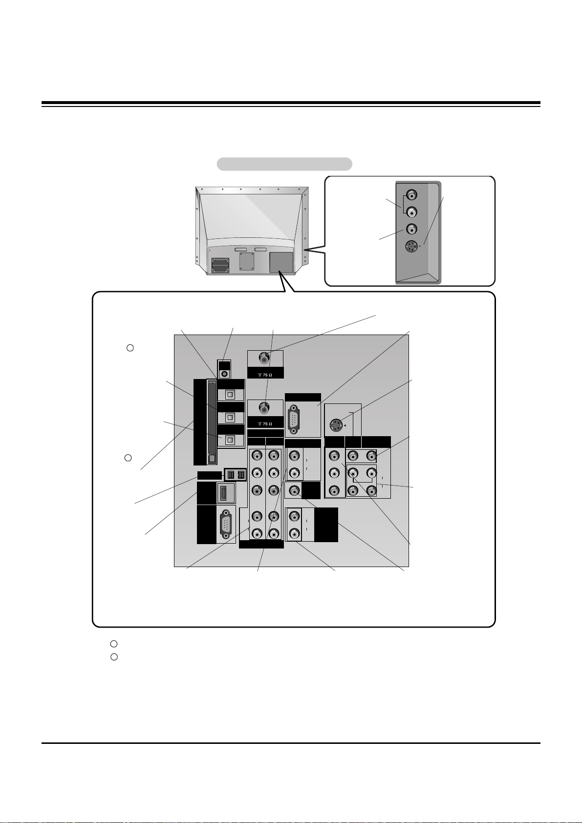
Connection Options
Connection Options
PC/DTV
(XGA
/480p
/720p
/1080i)
S-VIDEO
PR
PB
Y
MONO
CABLE
RGB INPUT
COMPONENT
INPUT2 INPUT1
DTV/DVD INPUT
RGB/DVI INPUT
(L)
(R)
AUDIO
(L)
(R)
AUDIO
VIDEO
(L)
(R)
AUDIO
(L)
(R)
AUDIO
AUDIO
CENTER
MODE IN
MONITOR
OUTPUT
VIDEO
INPUT2
VIDEO
INPUT1
DIGITAL AUDIO
OPTICAL INPUT1
(COMPONENT2)
DIGITAL AUDIO
OPTICAL INPUT2
(DVI)
IEEE1394
DIGITAL AUDIO
OPTICAL OUTPUT
ANTENNA
S-VIDEO
FRONT A/V
VIDEO
AUDIO
(R)
(L)/
MONO
Cable
CARD
HDMI/
DVI(VIDEO)
UPGRADE
PORT
VARIABLE
AUDIO OUT
G-LINK
Back Connection Panel
Back Connection Panel
ANTENNA Inputs
Connect antenna signals to the
TV directly .
DIGITALAUDIO OPTICAL
OUTPUT
Used to connect either an external amplifier, or add a subwoofer to your surround sound
system if it has a digital
audio optical input.
(Refer to )
MONITOR OUTPUT
Connect a second TV or
Monitor.
S-VIDEO In
A connection available
with some high-end
equipment that provides
even better picture quality for Video 2.
RGB/DVI INPUT
Connect the monitor
output connector from
a PC to the appropriate input port.
RGB Input
Connect the TV output
connector from a PC/DTV
to the appropriate input
port.
AUDIO CENTER MODE IN
Connect to external Dolby
Digital Center “preamp
output.”
VARIABLE AUDIO OUT
Used to connect either
an external amplifier, or
add a sub-woofer to your
surround sound system.
COMPONENT INPUT 1-2
Connect a component
video/audio device to these
jacks. Refer to your DVD
manual for further information.
VIDEO 1 or 2
Connects the video signals from various types
of equipment.
Left/Right AUDIO
Used for stereo sound
from various types of
equipment.
HDMI/DVI(VIDEO)
Connect a
HDMI/DVI(Video) signal
to this jack.
IEEE1394
Connect DVHS or
MicroMV to IEEE1394
Connector.
CableCARD
Used for CableCARD
received Cable Service
Provider.
CABLE Inputs
Connect cable signals to the
TV, either directly or through
your cable box.
LEFT/RIGHT AUDIO
Used for stereo
sound from various
types of equipment.
VIDEO
Connects the
video signals from
any piece of
equipment.
S-VIDEO
A connection
available on
some very
high-end equipment that provides better picture quality
than video
input.
G-LINK
Connect an
IR controller
to this jack.
DIGITALAUDIO OPTICAL INPUT1(COMPONENT2)
Connect digital audio
from the equipment
whose video is connected to COMPONENT 2.
DIGITALAUDIO OPTICAL INPUT2(DVI)
Connect digital audio
from the equipment
whose video is connected to
HDMI/DVI(VIDEO).
(Refer to )
Note: In standby mode, these port will not work.
If the video is connected through HDMI-TO-HDMI cable, you don’t need to connect digital audio. This port
is used only when the video connected through DVI-TO-HDMI cable.
1
2
1
2
DESCRIPTION OF CONTROLS
Page 7

- 7 -
LIGHT
TV/VIDEO
MODE
COMP/RGB/HDMI
MUTE
SURF
VOL CH
PGUP
PGDN
INFO
SAP
RATIO
CC
MENU
TV GUIDE
TIMER
EXIT
PLAY
PAUSE STOP
RECORD
PIP PIPCH- PIPCH+ PIPINPUT
ENTER
SIGNAL SWAP
REW FF
POWER
1394
FLASHBK
VIDEO
SOUND
ADJUST
FREEZE
DAY +
DAY -
SKIP
Remote Control Key Functions
Remote Control Key Functions
- When using the remote control, aim it at the remote control sensor on the TV.
VCR/DVD BUTTONS
Control some video cassette recorders or
DVD player ("RECORD" button is not available for DVD player.)
Selects the frequency setting in the recording: Once, Regulary, Weekly, Off.
RATIO
Changes the aspect ratio.
MODE
Selects the remote operating mode: TV,
VCR, DVD, CABLE, HDSTB or AUDIO.
Select other operating modes, for the
remote to operate external devices.
POWER
Turns your TV or any other programmed
equipment on or off, depending on mode.
1394
SURF
Use to scroll the Surf channel.
CC
Select a closed caption:
Off, CC1~4, Text1~4.
FLASHBK
Tunes to the last channel viewed.
CHANNEL UP/DOWN
Selects available channels found with EZ
scan.
PAGE UP/PAGE DOWN
Moves from one full set of screen information to the next one.
EXIT
Clears all on-screen displays and returns to
TV viewing from any menu.
TIMER
Lets you select the amount of time before
your TV turns itself off automatically.
PIP
Switches between PIP, POP (Picture-out-ofPicture) and Twin picture modes.
Switches the video window locking or
unlocking in the Listing Grid.
PIPCH-/PIPCH+
Changes to next higher/lower PIP channel.
PIP INPUT
Selects the input source for the sub picture.
SWAP
Exchanges the main/sub images in
PIP/Twin picture mode.
DAY+/DAY-
Moves forward or backward in 24 hour
increments in the Listings Grid.
LIGHT
Illuminates the remote control buttons.
TV/VIDEO
Selects: Antenna,Cable,Video1,2, Front
Video, Component 1-2, RGB-DTV (or RGB-
PC), HDMI/DVI input sources.
COMP/RGB/HDMI
Selects: Component 1-2, RGB-DTV (or RGB-
PC), HDMI/DVI input sources.
NUMBER buttons
DASH
Used to enter a program number for multiple
program channels such as 2-1,2-2,etc.
MUTE
Switches the sound on or off.
THUMBSTICK (Up/Down/Left/Right/ENTER)
Allows you to navigate the on-screen menus
and adjust the system settings to your pref-
erence.
VOLUME UP/DOWN
Increases/decreases the sound level.
SAP
Selects MTS sound: Mono, Stereo, and SAP
in Analog mode. Change the audio language
in DTV mode.
MENU
Brings up the main menu to the screen.
Enter or exit the panel menu in the Guide
Screen.
INFO
When you watch the TV, displays information
on top of the screen. Not available in
Component 1-2, RGB and HDMI/DVI mode.
TV GUIDE
Brings up the TV Guide On Screen system to
the screen.
VIDEO
Adjusts the factory preset picture
according to the viewing
environment.
ADJUST
Adjusts screen position, size, and
phase in PC mode.
SOUND
Selects the sound appropriate
for the program's character.
SIGNAL
Displays the digital signal strength.
FREEZE
Freezes the currently-viewed picture. Main pic-
ture is frozen in PIP/Twin picture mode.
DESCRIPTION OF CONTROLS
Page 8
- 8 -
ADJUSTMENT INSTRUCTIONS
1. Application Object
These instructions apply to the DLP Projection (Chassis: NB04AA).
2. Notes
(1) Because this is not a hot chassis,it is not necessary to use
an isolation transformer. However, the use of an insolation
transformer will help protect test equipment.
(2) The adjustments must be performed in the correct
sequence.
(3) The adjustments must be performed in the condition of
25±5°C of temperature and 65±10% of relative humidity if
there is no other specific designation.
(4) The input voltage of the receiver must remain AC 110V,
60Hz.
(5) Unless stated otherwise, the set must be operated for at
least 5 minutes prior to adjustments.
The heat-run should be performed with a 100% white
pattern,but reception of a moving picture may also be
possible in unavoidable cases.
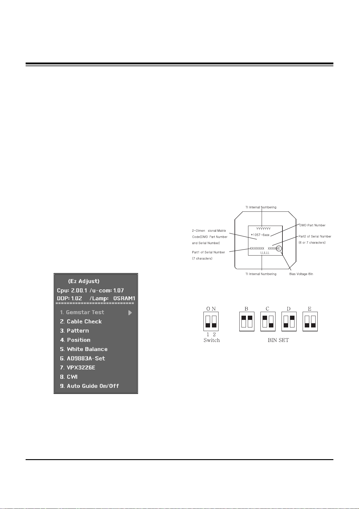
3. Composition of Adjustment Mode
(1) Adjustment modes are entered by pressing the ADJ key
on the Service Remote Control, after adjustments press
the ADJ key to exit.
(2) Initial Adjustment mode Menu is shown below. <Fig. 1>
(3) As shown <Fig. 1>, using the CH+ (
D), CH- (E) keys to
select an item, press the ENTER or VOLUME+ (
G) keys to
enter the appropriate item and begin adjustment.
(4) Change the value of adjustment with using the volume +(
G ),
volume -(
F) keys. To change adjustment item, use the
CH+ (
D), CH- (E) keys in EZ ADJ Mode.
(5) Press the ADJ key to exit, after adjustments.
(6) Preparation for Adjustment
1) Connect the power to TV Set and set “Power on”.
2) Allow set to Heat-Run for at least 5 minitues before
adjusting.
4. Driver Board Bin Setting
See Bias Voltage Bin on the DMD as shown <Fig. 2> and
adjust the switches on the lower Driver Board as shown <Fig.
3>.
<Fig. 2> DMD Marking Locations
<Fig. 1> Adjustment Mode OSD
<Fig. 3> Driver Board Bin Setting
Page 9
- 9 -
ADJUSTMENT INSTRUCTIONS
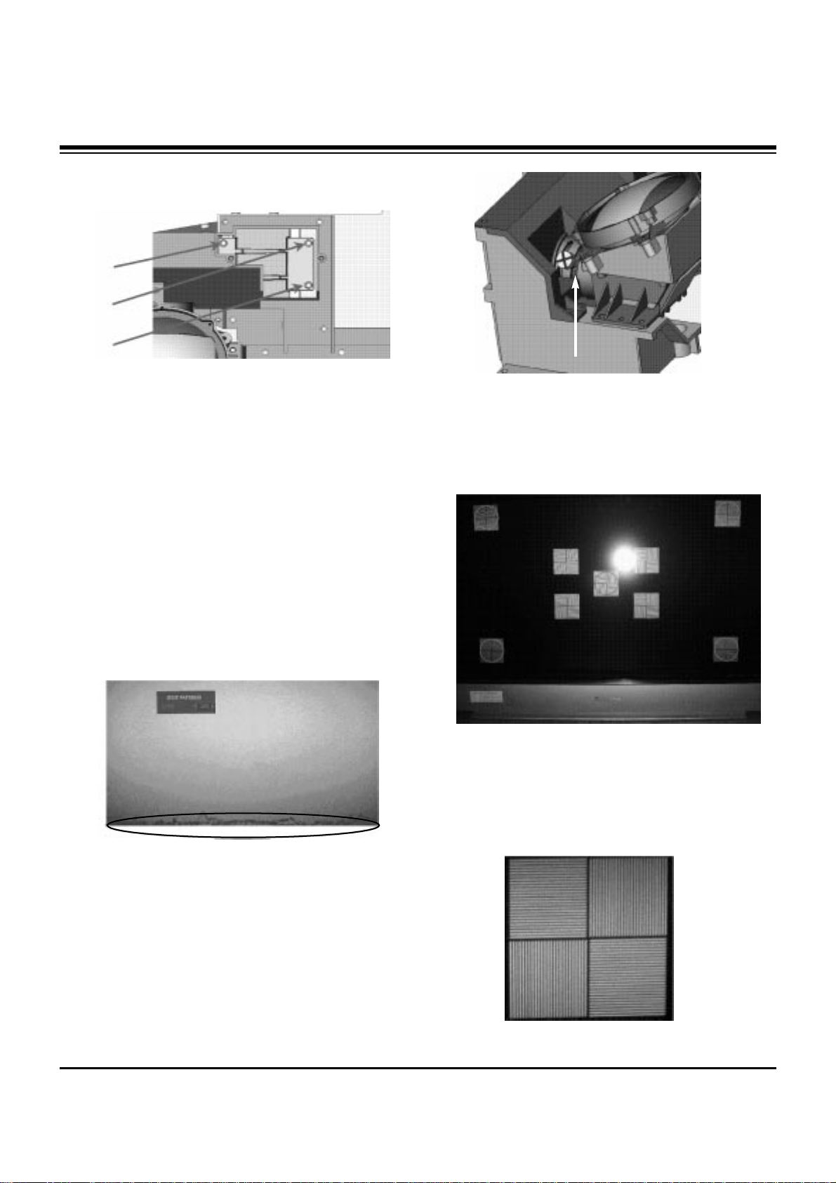
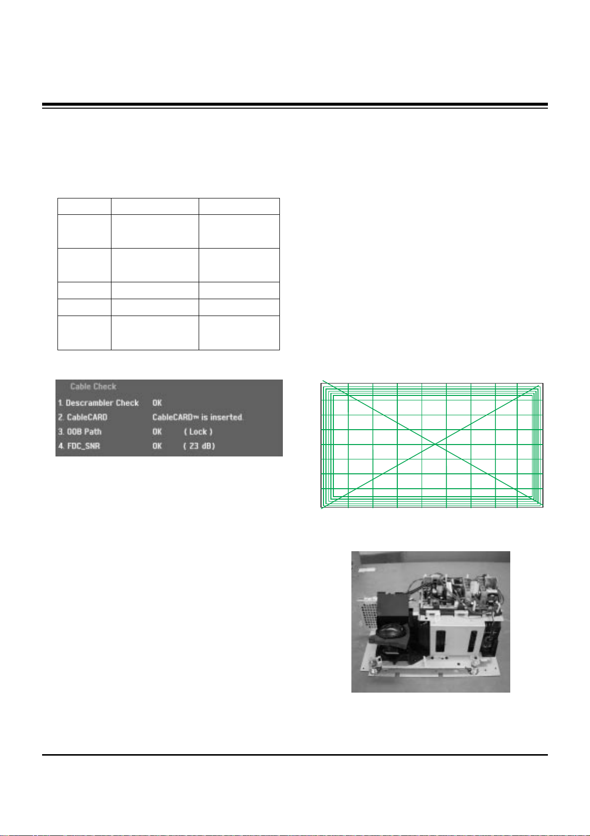
5. Adjusting the Optical Engine
(1) After placing the optical engine on the JIG, adjust
illuminator by adjuting the A, B, and C as shown <Fig. 4>.
1) Screen change when adjusting screw A
Tighten the screw: Upper/right illuminator are out of joint
Loosen the screw: Lower/left illuminator are out of joint
2) Screen change when adjusting screw B
Tighten the screw: Lower illuminator is out of joint
Loosen the screw: Upper illuminator is out of joint
3) Screen change when adjusting screw C
Tighten the screw: Upper/left illuminator are out of joint
Loosen the screw: Lower/right illuminator are out of joint
Check the spot (phenomenon such as Light tunnel exit) on the
edge of the white screen as shown <Fig. 5>.
(2) After adjusting the illuminator, adjust the focus by using the
focus adjustment screw of projection lens. After adjusting,
fasten the screw tighty and secure with sealer.
[ Note: The focus check point is not the screen center but the
upper/lower screen.
1) <Fig. 7> shows the pattern for focus adjustment
2) Adjust the 4 green ellipse so that all are in equal focus.
3) If you can’t check the DMD cell border at red center
position after adjustment, regard as NG.
4) <Fig. 8> shows the magnified pattern for checking the
focus adjustment
<Fig. 5>
<Fig. 6>
<Fig. 7>
<Fig. 8>
A
B
C
<Fig. 4>
Page 10
- 10 -
ADJUSTMENT INSTRUCTIONS
6. Caution for DMD
(Digital Micro-mirror Device)
6-1. Caution for DMD ESD
(1) Use a grounding strap to prevent ESD (Electrostatic
Dischage) damage when handing the DMD.
(2) Connect the grounding strap to a ground point on the
workbench.
(3) Keep the DMD in an ESD Safe container when not being
used or in transit.
(4) Wearing gloves will help prevent ESD damage and help
preserve the physical condition of the DMD.
(5) All work should be performed in a static free environment.
(6) Use caution and remove any dust particles on the DMD
front glass or back pins/pads.
6-2. Caution for DMD Cleaning
(1) Use caution to prevent scratches to the DMD glass.
(2) When DMD glass stains with dust, polish the front and
back DMD glass with soft cloth. Then, rotate the DMD 180
degrees and polish again.
(3) Do not use pressure when cleaning the DMD. The static
electricity and pollution can damage the DMD.
7. EDID(HDMI) Data Input
7-1. Required Test Equipment
(1) Jig for adjusting PC, DDC (PC serial to D-sub connection
device)
(2) S/W for writing DDC(EDID data write & read)
(3) D-sub terminal
(4) Jig for connecting EDID(HDMI) Cable
7-2. Adjustment Preparation and Setting of
Device
(1) Setup as in <Fig. 9> and turn on the PC & JIG.
(2) Operate the S/W for writing DDC(EDID data write & read)
(operated in DOS mode.)
8. CPLD Download Work
8-1. Required Test Equipments &
Preparation for Adjustment
(1) Connect the PC and memory JIG as shown in <Fig. 10>.
(2) Turn on JIG MAIN POWER SW.
(3) Turn on the PC and moniter, operate the device
programming software.
8-2. Adjustment Sequence
(1) Once the program is running, [OPTION MODE
SELECTION] is displayed in the window.
Check the “Load configuration File(.cdf, .pdr)” in this
window and click the finish button
(2) When the screen displays the open window, select the
suitable file(*.cdf) according to model.
(3) IC figure is change to green by clicking it.
(Refer to <Fig. 11>)
<Fig. 9> Device Setting Diagram of Input EDID Data
<Fig. 10 > How to connect the MEMORY JIG and PC
<Fig. 11>
Page 11
- 11 -
ADJUSTMENT INSTRUCTIONS
(4) Select program options.
(5) Check the [Erase before programming] and [Verify] menu
as shown <Fig. 12> and press the OK button.
(6) At this time, the download starts. The download will finish
in about 10 seconds.
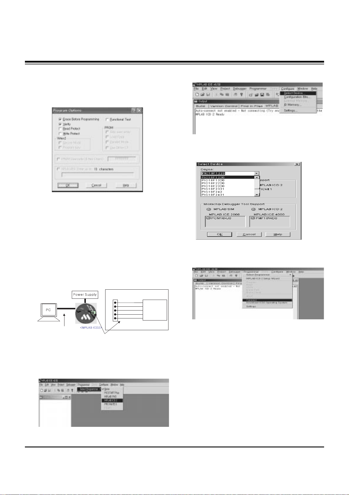
9. Gemstar VBI Micom Download
9-1. Preparation for Adjustment
(1) As shown below, connect the MPLAB ICD2 equipment, PC
and Digital Connector.
(2) Turn on the MPLAB ICD2 POWER Supply.
(3) After turning on the PC and MONITOR, select the ‘MPLAB
IDE’ from the screen.
9-2. Adjustment Sequence
(1) Once the program is executed, select the MPLAB ICD2
from "Programmer -> Select Programmer".
(2) Select "Configure -> Select Device".
(3) When the "Select Device" window appears, select the
PIC18F1220 from "Device" and press OK.
(4) Select "Programmer -> Connect".
When connected with the Micom, the display message on
the Output window appears as below.
<Fig . 12>
+13V
CN1201
IC1204
VIB Micom
+5V
GND
Data
Clock
<Digital Board>
Connect the MPLAB ICD2 and connector of Digital Board
Connect the RS-232 or USB Cable
Connecting to MPLAB ICD 2
...Connected
Setting Vdd source to MPLAB ICD 2
Target Device PIC18F1220 found, revision = 0x4
...Reading ICD Product ID
Running ICD Self Test
...Passed
MPLAB ICD 2 Ready
Page 12

- 12 -
ADJUSTMENT INSTRUCTIONS
(5) Select "File -> Import", select the Work HEX file and open.
(6) Select "Programmer -> Program".
(7) Download begins and about 3 seconds later, the
"Programming succeeded" message is displayed on the
Output window and the Download process is ended.
Note: Step (6) is more convenient when using the short-cut icon.
10. Gemstar IR Micom Download
10-1. Preparation for Adjustment
(1) As shown below, connect the MPLAB ICD2 equipment, PC
and Digital Connector.
(2) Turn on the MPLAB ICD2 POWER Supply.
(3) After turning on the PC and MONITOR, select ‘MPLAB
IDE’ from the screen.
10-2. Adjustment Sequence
(1) When the program is executed, select MPLAB ICD2 from
"Programmer -> Select Programmer"
(2) Select "Configure -> Select Device".
(3) When the "Select Device" window appears, select
PIC18F242 from "Device" and press OK.
(4) Select "Programmer -> Connect".
+13V
CN1203
IC1205
IR Micom
+5V
GND
Data
Clock
<Digital Board>
Connect the MPLAB ICD2 and connector of Digital Board
Connect the RS-232 or USB Cable
Page 13
- 13 -
ADJUSTMENT INSTRUCTIONS
When connected with the Micom, the display message on
the Output window appears as below.
(5) Select "File -> Import", select the Work HEX file and open.
(6) Select "Programmer -> Program".
(7) Download begins and about 3 seconds later, the
"Programming succeeded" message is displayed on the
Output window and the Download process is ended.
Note: Step (6) is more convenient when using the short-cut icon.
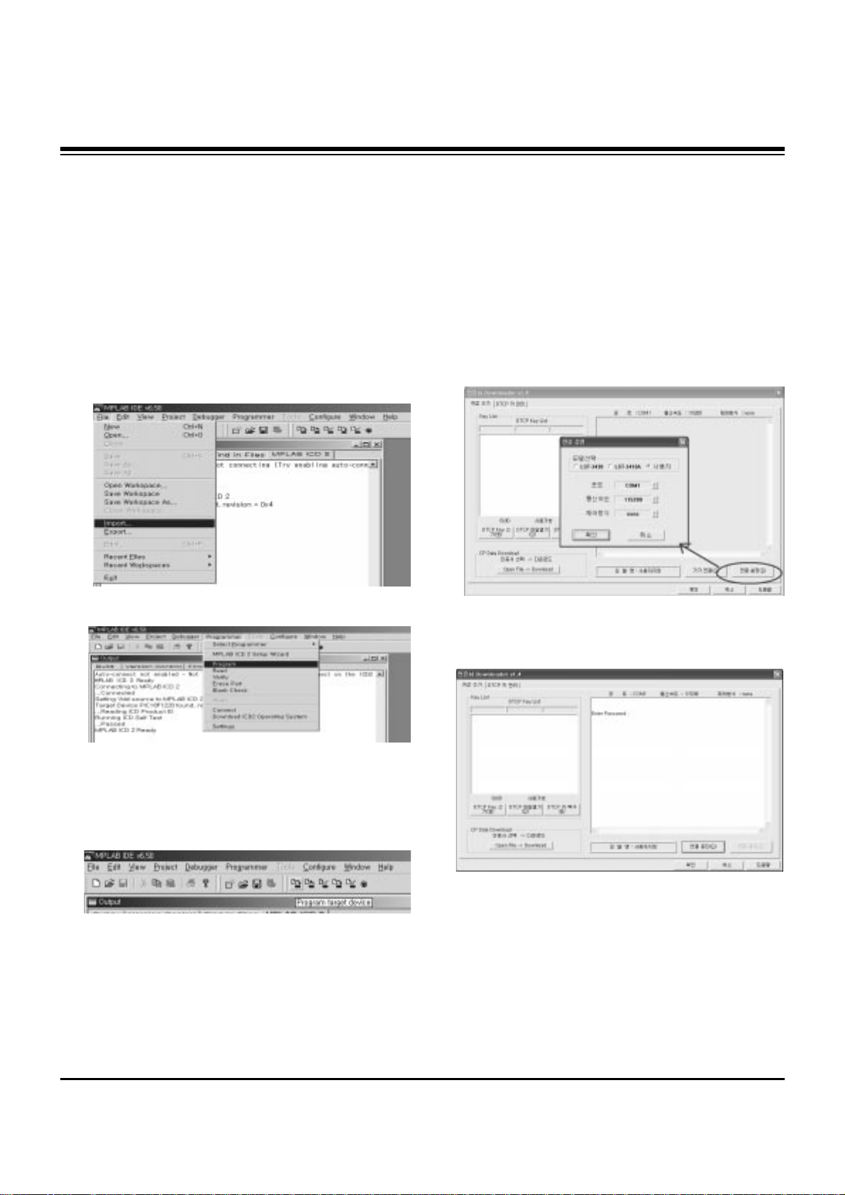
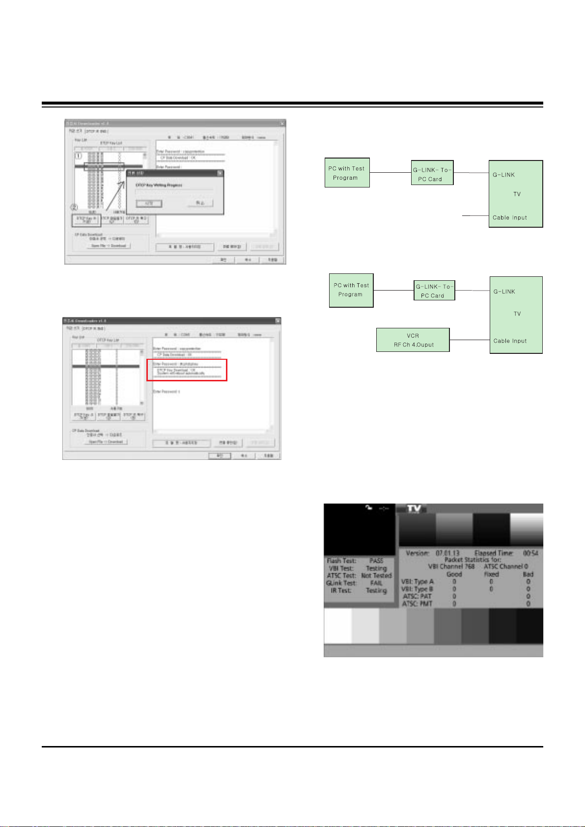
11. POD Certificate Download &
IEEE1394(DTCP) Download
11-1. Preparation for Adjustment
(1) Connect the MEMORY JIG and PC.
(2) Turn on the JIG MAIN POWER SWITCH.
(3) After turning on the PC and MONITOR, execute the
‘Certificate Downloader v1.4’ from the screen.
11-2. Adjustment Sequence
(1) After opening the ‘Certificate Downloader v1.4’, enter
Connection set and set the as same below.
The port settings are determined by each PC's setup.
(2) Select ‘Connection’ and SET connected to RS-232C.
(3) After clicking "Enter", confirm that "Enter Password:"
appears.
(4) Click the "OpenFile - Download" button from CP Data
Download, ‘select the Private Key’ appears and click
ENTER.
Connecting to MPLAB ICD 2
...Connected
Setting Vdd source to MPLAB ICD 2
Target Device PIC18F242 found, revision = 0x7
...Reading ICD Product ID
Running ICD Self Test
...Passed
MPLAB ICD 2 Ready
Page 14

- 14 -
ADJUSTMENT INSTRUCTIONS
(5) After clicking ENTER, the ‘opens Private key' window
appears and select the Private key applied to the SET.
The Private Key file name is on the Label of the Digital
Board.
(6) When the Dialog window appears, click OK and the
write work will begin.
(7) When completed, click ‘CP Data Download: OK’
[ When ‘CP Data Download: OK’ does not appear, certificate
has not Download correctly.
SET is rebooted and certificate Download work must be
repeated.
(8) Now, you may begin IEEE1394 (DTCP) Download work.
Select the “DTCP.dat” file by pressing the ‘DTCP File
Open’ button.
(9) After opening the ‘DTCP.dat’ file, confirm the key list in the
DTCP Key List window.
(10) Select the desired item of DTCP key List.
When pressing ‘DTCP key writing’ button, the Progress
window will appear.
Page 15
- 15 -
ADJUSTMENT INSTRUCTIONS
(11) When completed, “DTCP key Download: OK" will display
in the Terminal window and the SET will reboot
automatically.
[ When process (11) malfunctions, it is not Download.
DTCP Download process start again from (8).
12. Gemstar Operation Confirmation
12-1. Required Test Equipment
(1) PC with Factory Test Program
(2) G-LINK-To-PC Card (Serial GLINK(CN1202))
(3) VBI Inserter (Norpak TES3) - Guide Data Discharge
Equipment
[ If the VBI Inserter(TES3) is not available, a VCR may be
used.
12-2. Preparation for Adjustments
(1) When using VBI Inserter(TES3): Signal uses Cable input
and set as below.
(2) When not using VBI Inserter(TES3): VCR uses Cable input
and set as below.
[ Factory Test S/W must be set to "GLinkTo PC Card" ON.
12-3. Adjustment Confirmation Work
(1) Turn on the TV and run Factory Test Program of PC.
[ Program only needs to run once, regardless of set quantity.
(2) Enter the EZ adjust menu by pressing Adjust on the
Service Remote Control (S R/C).
(3) Go to number 1 Gemstar and press Enter.
(4) TV set screen will appear as shown.
(5) Confrim that VBI Test, Glink Test and IR Test PASS from
the screen.
Input Signal
Page 16
- 16 -
ADJUSTMENT INSTRUCTIONS
13. Cable Operation Confirmation
(1) Confirm that the Cable Card is inserted in the slot.
(2) Enter the EZ adjust menu by pressing Adjust on the
Service Remote Control (S R/C).
(3) Go to number 2 Cable Check and press the Right key (
G) .
(4) Confirm items below..
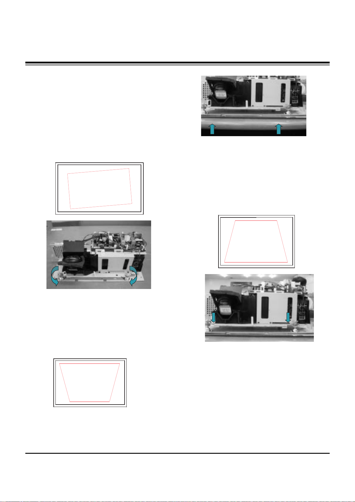
14. Tilt & Keystone Adjustment
14-1. Required Test Equipment
(1) Hardware: Six angle wrenches, Spanner, and Screwdriver
(2) PC to output XGA signal
(3) Service Remote Control
14-2. Preparation for Adjustment
(1) Engine Fix Knob will be able to adjust, Lower Back Cover
does not close.
(2) After Set turn on, select the adjustment pattern come out
from screen using EYE Key on the Service Remote Control .
14-3. Adjustment
(1) After Engine to be completely affixed in the adjustment
Knob pillar from TV front, sees camera sheds light TV
Screen and Keystone & Tilt confirm from back side.
(2) Keystone adjust moving to upper, lower with Top, Bottom
adjustment BOLT and Tilt adjust moving to left, right with
Engine Base.
(3) Both sides Adjustment Knob and Top Mirror adjust to be
Tilt and Keystone is Max and Min difference 4mm.
(4) After adjustment completed, Engine fixes with Top fixation
BOLT.
Name
Descrambler
Check
CableCARD
OOB Path
FDC_SNR
Video Signal
Normal
OK
CableCARD
TM
is inserted.
OK(Lock)
OK(20dB above)
Normal Screen
Defective
Not OK
CableCARD
TM
is removed.
Not OK(Unlock)
Not OK(20dB under)
Black Screen
(No Picture)
<Tilt & Keystone Adjustment Pattern>
<DLP Engine>
Page 17
- 17 -
ADJUSTMENT INSTRUCTIONS
14-4. It followed in Screen Condition,
Projector Lens Direction
(1) When the upper portion of the screen is larger than the
bottom: Adjust Projection lens upward
(2) When the upper portion of the screen is smaller than the
bottom: Adjust Projection lens downward
14-5. It followed in Screen Form,
Adjustment Method
(1) When the screen is rotated: Rotate the Engine to adjust
1) Badness Type: Tilt Badness
2) Adjustment Method:
Engine Base rotate with the left/right and fix the
horizontality horizontal line of Cross Pattern
(2) In case of the upper screen size is large bottom screen
size than: upward projector
1) Badness Type: Keystone Badness
2) Adjustment Method:
The Engine Base front part raises at upper direction and
projection lens to be downward projector.
Bottom screen size a lot, fix the top/bottom screen size to
be same as.
(3) In case of
the upper screen size is
smaller
bottom screen
size than:
downward projector
1) Badness Type: Keystone Badness
2) Adjustment Method:
The Engine Base front part down at bottom direction
and projection lens to be upward projector.
Top screen size a lot, fix the top/bottom screen size to
be same as.
Page 18

- 18 -
ADJUSTMENT INSTRUCTIONS
15. Screen Position Adjustment
15-1. Required Test Equipment
Service Remote Control
15-2. Horizontal Position Adjustment
(1) Press ADJ key on the remote control to enter the
adjustment mode.
(2) Select POSITION in the adjustment menu.
(3) The adjustment pattern below appears.
(4) Select the H_position with CHANNEL key.
(5) Change data with using the VOLUME keys on the remote
control in order adjust left/right screen semmetry.
(6) If symptom is out of adjustable range: N.G.
(7) After adjustment is completed, recieve NTSC-M Digital
Pattern and check the adjusment level.
15-3. Vertical Position Adjustment
(1) Select V_position with CHANNEL key. (V: 15)
(2) Change data with using the VOLUME keys on the remote
control in order to adjust up/downscreen semmetry.
(3) If symptom is out of adjustable range: N.G.
16. Component AD9883A Offset/
Gain Adjustment
16-1. Required Test Equipment
Service Remote Control, 801GF/802F Pattern Generator
16-2. Preparation for Adjustment
(1) Connect power and turn TV set on.
(2) Perform Heat-Run for at least 5 minutes.
(3) Select Component Input.
(4) Receive the 720P/60Hz, HozTVBar Pattern of 801GF/802F.
16-3. Offset/ Gain Adjustment
(1) Press ADJ key on the Remote Control to enter the
adjustment mode after more than 10 seconds of receiving
the signal.
(2) Adjustment is automatic by pressing the VOLUME+ (
G)
key in AD9883A-SET item of adjustment menu.
“Gain/Offset Adjust” will apeear on the OSD for a short
time during adjustment.
(3) After adjustment, “End of AD9883 Adjust” appears and
press the ADJ key to exit.
<Pattern for Screen Adjustment>
Adjustment
Adjustment
<720P/60Hz HozTVBar Pattern>
Page 19

- 19 -
ADJUSTMENT INSTRUCTIONS
17. White Balance Adjustment
17-1. Required Test Equipment
CA110 or CA210
17-2. White base value (Medium)
x = 0.283¡ 0.01, y = 0.297¡ 0.01
17-3. Adjustment
(1) Install the equipment(CA110 or CA210) be 20cm away
from screen center.
(2) Select White balance by pressing ADJ Mode Key on
Remote control.
(3) Warm(6500
cK) : x = 0.313, y = 0.329
1) R Gain 107 fixation
2) Adjust white balance changing G, B gain.
3) Offset fixation R/G/B --> -20, -20, -20
(4) Medium(9300cK) : x = 0.283, y = 0.297
1) R Gain 107 fixation
2) Adjust white balance changing G, B gain.
3) Offset fixation R/G/B --> -20, -20, -20
(5) Cool(12000cK) : x = 0.275, y = 0.277
1) R Gain 107 fixation
2) Adjust white balance changing G, B gain.
3) Offset fixation R/G/B --> -20, -20, -20
* Reference : Gamma table -> 1
Brightness -> 200Level
Spoke Func. -> 0
R/G/B offset -> Fix to -20 without MODE
18. CWI Adjustment
18-1. Required Test Equipments
Service Remote Control
18-2. Preparation for Adjustment
(1) Connect power and turn the TV set on.
(2) Using the remote control, enter from ADJUST to CWI.
(Base value: 160)
18-3. Adjustment
(1) Using the Volume key, adjust CWI to the left/right.
(2) As adjustment, check the appearance noise in the TEST
Pattern.
Setting the value reduced 3~4 step at a GREEN noise
disappearing spot.
(3) Using CH UP/DOWN key of the Remote Control, enter the
RED PATTERN.
(4) Check the RED Pattern to uniform. After checking unless
abnormality do OK.
[ As temperature is different sensitivity, change angle of the
color wheel. At this time, the adjustment is done because color
may be changed.
(color wheel index)
CWI
160
<TEST Pattern: Lamp Gray Pattern>
(color wheel index)
CWI
162
starting point of noise
(appearance GREEN)
(color wheel index)
CWI
160
<TEST Pattern: RED Pattern>
Page 20

- 20 -
ADJUSTMENT INSTRUCTIONS
19. Main/Sub Contrast Adjustment
Adjust which it sees last prosecuting attorney time the screen
contrast difference.
Basically the letter does with the fact that the character and
distinction become.
19-1. Preparation for Adjustment
(1) Receive signal(RF 06Ch.) on the Main/Sub screen in twin
picture mode.
(2) Set Picture control to “CLEAR”.
19-2. Adjustment
(1) Main Screen Adjustment
1) Select the VPX3226 by pressing “ADJ” key on the
Service Remote Control.
2) Select Contrast(m) in adjustment menu using CH +/keys and adjust using VOL +/- keys. (Initial data: 32)
(2) Sub Screen Adjustment
1) Select the VPX3226 by pressing “ADJ” key on the
Service Remote Control.
2) Select Contrast(s) of adjustment item using CH +/-keys
and adjust using VOL +/- keys. (Initial data: 32)
19-3. Overseas Factory Production
Contrast Adjustment Method
Adjust which it sees last prosecuting attorney time the screen
contrast difference.
(1) Do the same method as above method.
(2) Make the as same below pattern in VHF 6CH using RF
MODULATOR and PATTERN GENERATOR.
(3) Adjust to become dividing 15 and 16 Gray of Main/Sub
screen .
(4) Adjust to be identical Main/Sub contrast of MAX 16Gray.
(5) Make the adjustment pattern as below.
<16Gray Scale/H Pattern>
Page 21

- 21 -
PRINTED CIRCUIT BOARD
MAIN(TOP)
Page 22

- 22 -
PRINTED CIRCUIT BOARD
MAIN(BOTTOM)
Page 23

- 23 -
PRINTED CIRCUIT BOARD
TUNER(TOP)
Page 24

- 24 -
PRINTED CIRCUIT BOARD
TUNER(BOTTOM)
Page 25

- 25 -
PRINTED CIRCUIT BOARD
DIGITAL(TOP)
Page 26

- 26 -
PRINTED CIRCUIT BOARD
DIGITAL(BOTTOM)
Page 27

- 27 -
PRINTED CIRCUIT BOARD
DRIVER(TOP)
DRIVER(BOTTOM)
Page 28

- 28 -
PRINTED CIRCUIT BOARD
SMPS
LINE FILTER
Page 29

- 29 -
PRINTED CIRCUIT BOARD
CONTROL(TOP)
CONTROL(BOTTOM)
PRE-AMP SIDE A/V
CASE DET
INTERFACE
COLOR WHEEL
Page 30

- 30 -
PRINTED CIRCUIT BOARD
LED(TOP)
LED(BOTTOM)
COMPONENT(TOP)
COMPONENT(BOTTOM)
Page 31

- 31 -
BLOCK DIAGRAM
Page 32

- 32 -
EXPLODED VIEW
410
680
681
401
403
402
404
700
630
420
640
641
602
622
623
174
502
530
590
601
600
570
572
571
612
620
610
611
621
720
411
310
308
309
305
660
121
300
650
301
120
302
430
434
431
433
432
670
520
540
501
550
624
560
503
400
Page 33

- 33 -
EXPLODED VIEW PARTS LIST
120 6400WESC01A SPEAKER,WOOFER C080P23K1450 ESTEC WOOFER 8OHM 15/25W 84DB 80 NON
121 6400DESA01A SPEAKER,TWEETER D016D01K1450 8HMOHM 15/25W 85DB 50 NON
174 6410VUH004A POWER CORD,UL/CSA3000MM 3P 3000MM HUG BLACK 500MH 7A
300 3091V00552C CABINET ASSEMBLY,DU-52SZ61D STEREO NB04AA FULL
301 5020V00870B BUTTON,CONTROL DN-52SZ60D ABS, HF-380 7KEY .
302 4811V00049C BRACKET ASSEMBLY,SPEAKER DU-52SZ61D NB04AA GRILLE,LG BRAND
305 3351V00007A SCREEN ASSEMBLY,RN-52SZ30H 1178*670*3.6 LCD TYPE
308 4980V00890B SUPPORTER,SCREEN SECC(EGI) SIDE(CUSHION),RN-52SZ50H
309 4980V00889B SUPPORTER,SCREEN EGI BOTTOM(CUSHION),RN-52SZ50H
310 4980V00888B SUPPORTER,SCREEN SECC(EGI) TOP
400 3809V00361F BACK COVER ASSEMBLY,RU-52SZ61D NON ZENITH
401 3550V00269D COVER,LAMP RU-44SZ51D PC-ABS FAN 7S00115A
402 3550V00322D COVER,LAMP RU-52SZ51D HIPS 40AF SIDE
403 3110V00307B CASE,LAMP DUCT DLP 52SZ60H PC-ABS .
404 4980V00885E SUPPORTER,BACK COVER SECC(EGI) FRONT,RN-52SZ50H
410 3809V00362F BACK COVER ASSEMBLY,RU-52SZ51D NON ZENITH
411 3550V00321C COVER,LAMP RU-52SZ51D HIPS 40AF ZENITH
420 3550V00365C COVER ASSY,RU-52SZ51D ABS, AF-303S DUST
430 5018V00067D MIRROR,REFLECTION SSC(SAMSUNG CORNING) 0000 1172(H1)*590(H2)*604(V1)*3T .
431 4810V01112A BRACKET,SUPPORTER TN-56SZ70LR NB037A NON MIRROR SIDE, LEFT
432 4980V00883C SUPPORTER,MIRROR AL TOP
433 4980V00884C SUPPORTER,MIRROR AL BOTTOM
434 4810V01113A BRACKET,SUPPORTER TN-56SZ70LR NB037A NON MIRROR SIDE, RIGHT
501 3210V00165B FRAME,ABS, AF-303S RN-48SZ40H MAIN CHASSIS
502 3210V00191A FRAME,CHASSIS HIPS 40AF DN-44SZ60D SMPS
503 4811V00135A BRACKET ASSEMBLY,REAR AV DU-52SZ62D NB04AA .
520 6871VMMR77A PCB ASSEMBLY,MAIN NB-04AA DU-44/52SZ60D
530 6871VPMA54A PCB ASSEMBLY,POWER SMPS NB-04AA DLP M/I
540 6871VSMS02A PCB ASSEMBLY,SUB TUNER NB03KB CABLE READY
550 6871VSMS01C PCB ASSEMBLY,SUB DIGITAL NB04AA DU-52SZ62D
560 6871VSMU24F PCB ASSEMBLY,SUB NB04AA DU-52SZ61D COMP M/I ASSY
570 6871VSMB50F PCB ASSEMBLY,SUB NB04AA DRIVER(DU-52SZ61D)
571 4814V00434B SHIELD ASSY,DN-44SZ60D NB03KB SUS ,SHIELD CASE DRIVE BOTTOM
572 4814V00394B SHIELD,COVER DN-44SZ60D NB03KB AL DRIVER FRONT DLP720P SHIELD CASE
590 6871VSMV52B PCB ASSEMBLY,SUB L/F NB037B TU-62SZ72D LINE-FILTER M/I
600 3141VSN906A CHASSIS ASSEMBLY,SUB NB03KB DU-44/52SZ60D
601 4980V00886B SUPPORTER,SMPS SECC(EGI) DLP
602 4980V00816C SUPPORTER,OPTICAL EGI DN-44SZ50D ENGINE BASE
610 6912B22007A LAMP,HIGH PRESSURE MECURY UHP 120W 1.0 PH E23 PHILIPS 120V 1A 25KV
611 4814V00396B SHIELD,COVER DN-44SZ60D NB03KB SECC(EGI) COVER,LAMP.DLP720P-ENGINE
612 4930V00301A HOLDER,PC+GF30% LAMP
620 5900V12001B FAN,DC G1225S12B2 DONGYANG 120*120*25 12V 1000RPM 9-14V L1000MM
621 4810V00813A BRACKET,FIXER RN-44SZ50H NB03JA ABS, AF-303S FAN HOLDER
622 5900V06006A FAN,DC F6025S12B2 DONGYANG 60*60*25 12V 2000RPM 9-14V L650MM
623 4980V00813B SUPPORTER,FAN SPCC(CR) ,DN-44SZ60H
624 5900V06006B FAN,DC F6025S12B2 DONGYANG 60*60*25 12V 2000RPM 9-14V L350MM
630 6871VSN221J PCB ASSEMBLY,SUB NB04AA PRE-AMP, DU-52SZ61D
640 6316000007A BALLAST,EUC-120P/H11 PHILIPS 20KV
641 4810V00659A BRACKET,BALLAST RE-44SZ20 NON ABS NON
650 6871VSMV96B PCB ASSEMBLY,SUB NB03KB TACT S/W
660 6871VSMV95D PCB ASSEMBLY,SUB LED MB03CC M/I ASSY FOR CHINA
670 6871VSME03K PCB ASSEMBLY,SUB NB04AA CASE S/W, DU-52SZ61D
680 6871VSN220D PCB ASSEMBLY,SUB NB037A TN-56SZ70LR SIDE AV M/I
681 3500V00061M BOARD ASSY,RU-44SZ51D NB03JC FRONT A/V
700 6871VSMY69A PCB ASSEMBLY,SUB INTER MB03CC M/I ASSY FOR CHINA
720 6871VSMW40E PCB ASSEMBLY,SUB SENSOR MB03CC HD2 7SEGMENT SENSOR B/D
No. Part No.
Description
Page 34

- 34 -
REPLACEMENT PARTS LIST
LOCA. NO PART NO DESCRIPTION
IC403
IC403
IC404
IC405
IC405
IC406
IC406
IC407
IC408
IC409
IC409
IC410
IC413
IC414
IC415
IC5
IC500
IC500
IC501
IC502
IC502
IC600
IC601
IC601
IC601
IC602
IC603
IC700
IC701
IC701
IC702
IC702
IC703
IC704
IC705
IC800
IC800
IC801
IC801
IC802
IC803
IC804
IC805
IC806
IC807
IC808
IC810
IC811
0IMMRSS041D
0ISH302122A
0ISH052100C
0ISH323422A
0ICTMLG013A
0ISH323422A
0INA562300A
0ISJ156612A
0ISS780500F
0IKE781200P
0IKE780500P
0ISH052100C
0IKE780900M
0IMCRFA009A
0ISH052100C
0IFA754207A
0IMCRFA013A
0IPRPTI001A
0ITO741570C
0ICB841500B
0IZZVF0020B
0ILNRMN005A
0IMCRMN012A
0IMCRNS006A
0ILNRMN005A
0IFA754207A
0ISS455880A
0IMCRTI011A
0IMCRXL004A
0IMMRAL015C
0IMCRTI019A
0IMCRFA003A
0ILNRID002A
0ILNRID002A
0IMCRAL006A
0IMCRSJ001A
0IMMRSS053B
0ICTMLG014B
0IMCRTI014A
0IMCRSG007A
0IMCRSG008A
0IMCRSG008A
0IMCRMX001A
0IMCRSG008A
0IMCRMX001A
0IMCRSG008A
0IMCRSJ001A
0IMCRON002A
K4S641632H-TL75 54P
PQ30RV21 TO-220
PQ05RD21 4SIP
PQ3RF23 4P(TO-220) 3.3V
LGDT1901A 24P
PQ3RF23 4P(TO-220) 3.3V
CLC5623IMX 14P
SC15661T-2.5TR 3P TO-220-3L
KA7805
KIA7812API TO220 ST 3P 12V
KIA78L05BP(AT) 3P 5V,150MA
PQ05RD21 4SIP
KIA7809API TO220 ST 3P 9V
KA78M08RTM 2P
PQ05RD21 4SIP
KA75420ZTA 3P,TO-92 TP 4.2V
74LCX244MTC 20P
TFP401PZP 100 DIGITAL RECEIVER
TC74LCX157FT 16P
CS8415A-CZR 28P 96KHZ DIGITAL AUDIO
X1272-0346 251P HD2
VPX3226E 44 VIDEO PIXEL DECODER
MSP4450G QA B8 80P MULTI SOUND
LM4765T 15P AUDIO POWER AMP
VPX3226E 44 VIDEO PIXEL DECODER
KA75420ZTA 3P,TO-92 TP 4.2V
KA4558D 8SOP OP AMP
2503227-001(DDP1010) 529P
XC95288XL-10TQ144C 144P
AT49BV8192A-90TI 48P
TFP410 64P
KA2903 8SOP
IDTQS4A210Q IDT 16P
IDTQS4A210Q IDT 16P
AT24C16AN-10SI-2.7 8P
SC1565IST-1.8 3P SOT223
K4R271669F-TCS8 54P
LGDT3302S 100P
CDCR83 24P
74VIT125CTR 5P S0T323-5L
74LX1G14CTR 5P SOT323-5L
74LX1G14CTR 5P SOT323-5L
MAX708SCSA 8P
74LX1G14CTR 5P SOT323-5L
MAX708SCSA 8P
74LX1G14CTR 5P SOT323-5L
SC1565IST-1.8 3P SOT223
MC33262P 8P
LOCA. NO PART NO DESCRIPTION
IC1
IC1
IC1
IC100
IC1000
IC1000
IC1001
IC1002
IC1004
IC1008
IC101
IC102
IC103
IC1101
IC1102
IC1105
IC1200
IC1200
IC1202
IC1202
IC1203
IC1204
IC1205
IC1301
IC151
IC152
IC152
IC1602
IC2
IC200
IC201
IC202
IC203
IC204
IC206
IC207
IC208
IC208
IC300
IC301
IC4
IC400
IC401
IC401
IC402
IC402
0IZZVC0119A
0IMCRSH003A
0IPRPTO002A
0IKE702900G
0IMCRTI025A
0IMI623200B
0IPRPFA006A
0IPRPFA007A
0IMMRNE002A
0IMI623200B
0ITK118100B
0ISTLPH026A
0IMCRBM003A
0ICTMLG017A
0IMCRLT002A
0IMCRFA013A
0IMCRSO008A
0IMCRMT003A
0IMO744053B
0IMO744053B
0IPMGNS026A
0IMCRMP006A
0IMCRMP007A
0ICTMLG018A
0IMCRTI035A
0IMCRFA004A
0ISS455880A
0ISH052100C
0IFA754207A
0IMCRAL021A
0IMMRHY015B
0IMMRHY015B
0IMMRAM006B
0IMMRAM006B
0IMCRSG010A
0IMCRPH026A
0ISO206900A
0IMO744053B
0IMCRSJ001A
0ICTMLG009A
0IMCRAL006A
0IMMRSS041D
0ISH122100B
0IMMRSS041D
0ISH302122A
0IMMRSS041D
M37272E8A(OTP) DIP 42P
GP2S40 4P
TC7S14F(T5L,T) 5P
KIA7029AF SOT-89 TP 2.9V
TSB43CA42GGW 176P
M62320FP 16P
RC1117S33T SOT-223 R/TP 3.3VOLT
RC1117S25T SOT-223 R/TP 2.5VOLT
UPD64083GF3BA 100
M62320FP 16P
TK11840L 8P SOT23L DC-DC CONVERTER
74LVC14APW 14PIN
IBM25PPC405CR-3BC200C
LGDT3502B 208P/PBGA
LCT1470CS8 8P
74LCX244MTC 20P
CXA2151Q 48P
MM1108XFFE 8P
MC74HC4053DW 16SOP 3*2CH.MUX
MC74HC4053DW 16SOP 3*2CH.MUX
LM311MX 8P
PIC18F1220T-I/SO 28P
PIC18F242T-I/SO 18P
LGDP4410 176P
TL592B-8DR 8P VIDEO AMPLIFIER
KA2904DTF 8SOP R/TP OP-AMP
KA4558D 8SOP OP AMP
PQ05RD21 4SIP
KA75420ZTA 3P,TO-92 TP 4.2V
AT24C512W-10SI-2.7 8P
HY57V281620HCT-H 54P
HY57V281620HCT-H 54P
AM29DL640H90EI 48P
AM29DL640H90EI 48P
ST3232CDR 16 R/TP RS232
PCA9516PW 16P
CXA2069Q QFP64 I2C BUS AV S/W
MC74HC4053DW 16SOP 3*2CH.MUX
SC1565IST-1.8 3P SOT223
LGDT1102 HD2 SBGA-432PIN
AT24C16AN-10SI-2.7 8P
K4S641632H-TL75 54P
PQ12RD21 4SIP
K4S641632H-TL75 54P
PQ30RV21 TO-220
K4S641632H-TL75 54P
IC
RUN DATE : 2004.8.30
For Capacitor & Resistors, the
charactors at 2nd and 3rd digit
in the P/No. means as follows;
CC, CX, CK, CN : Ceramic
CQ : Polyestor
CE : Electrolytic
RD : Carbon Film
RS : Metal Oxide Film
RN : Metal Film
RF : Fusible
Page 35

- 35 -
LOCA. NO PART NO DESCRIPTION
IC820
IC831
IC832
IC841
IC845
IC900
IC900
IC901
IC901
IC905
IC906
IC907
IC908
IC909
IC910
IC903
IC904
IC905
Q1000
Q1001
Q1001
Q1002
Q1002
Q1003
Q1003
Q1004
Q1004
Q1005
Q1005
Q1006
Q1007
Q1008
Q1009
Q101
Q1010
Q1011
Q1012
Q1013
Q1014
Q1015
Q1016
Q1017
Q102
Q107
Q109
Q1200
Q1200
Q1201
Q1202
0ISK666813A
0ISK615311B
0ISH817300B
0ISH817300B
0IMCRKE003B
0IMCRAD002A
0IMCRTI012B
0IMCRTI013A
0IMCRS5005A
0IMMRAL014B
0IMCRSG007A
0IMCRSG008A
0IMCRSG008A
0IMCRSG008B
0IMCRSG007A
0TFFC80015A
0TFFC80015A
0TFFC80015A
0TR387500AA
0TR387500AA
0TR387500AA
0TR387500AA
0TR387500AA
0TR387500AA
0TR387500AA
0TR150400BA
0TR387500AA
0TR150400BA
0TR387500AA
0TR387500AA
0TR150400BA
0TR150400BA
0TR387500AA
0TR387500AA
0TR150400BA
0TR150400BA
0TR150400BA
0TR150400BA
0TR387500AA
0TR150400BA
0TR387500AA
0TR150400BA
0TRKE80038A
0TR387500AA
0TR387500AA
0TR387500AA
0TRKE80046A
0TR387500AA
0TR387500AA
STR-F6668B(LF1352) 5PIN
STR-G6153T(LF1101) 5PIN
PC817XF3 4D PHOTO COUPLER
PC817XF3 4D PHOTO COUPLER
KIA78R12API 4P TO-220IS
AD9883AKST-110 80P DIGITAL BOARD
2503253-0003(DAD1000-3) 80P
SNSH6742CFA0PA(P32J6742PAG) 64P
SIL9993CTG100 100P
AT24C02N-10SI-2.7 8P
74VIT125CTR 5P S0T323-5L
74LX1G14CTR 5P SOT323-5L
74LX1G14CTR 5P SOT323-5L
74LX1G07CTR 5P SOT323-5L
74VIT125CTR 5P S0T323-5L
FDS6930A 8P O-8 30V 5.5A
FDS6930A 8P SO-8 30V 5.5A
FDS6930A 8P SO-8 30V 5.5A
CHIP 2SC3875S(ALY) KEC
CHIP 2SC3875S(ALY) KEC
CHIP 2SC3875S(ALY) KEC
CHIP 2SC3875S(ALY) KEC
CHIP 2SC3875S(ALY) KEC
CHIP 2SC3875S(ALY) KEC
CHIP 2SC3875S(ALY) KEC
CHIP 2SA1504S(ASY) KEC
CHIP 2SC3875S(ALY) KEC
CHIP 2SA1504S(ASY) KEC
CHIP 2SC3875S(ALY) KEC
CHIP 2SC3875S(ALY) KEC
CHIP 2SA1504S(ASY) KEC
CHIP 2SA1504S(ASY) KEC
CHIP 2SC3875S(ALY) KEC
CHIP 2SC3875S(ALY) KEC
CHIP 2SA1504S(ASY) KEC
CHIP 2SA1504S(ASY) KEC
CHIP 2SA1504S(ASY) KEC
CHIP 2SA1504S(ASY) KEC
CHIP 2SC3875S(ALY) KEC
CHIP 2SA1504S(ASY) KEC
CHIP 2SC3875S(ALY) KEC
CHIP 2SA1504S(ASY) KEC
KTC3552T-RTK SOT-23F 50V 3A
CHIP 2SC3875S(ALY) KEC
CHIP 2SC3875S(ALY) KEC
CHIP 2SC3875S(ALY) KEC
2N3904S SOT23 60V 200MA
CHIP 2SC3875S(ALY) KEC
CHIP 2SC3875S(ALY) KEC
LOCA. NO PART NO DESCRIPTION
Q1202
Q1203
Q1203
Q1204
Q1205
Q1206
Q1206
Q1207
Q1208
Q1209
Q1210
Q1213
Q1214
Q1215
Q1216
Q1217
Q1218
Q1219
Q2
Q201
Q202
Q203
Q204
Q205
Q206
Q207
Q208
Q209
Q210
Q211
Q3
Q403
Q5
Q6
Q601
Q601
Q602
Q602
Q602
Q603
Q604
Q605
Q605
Q605
Q614
Q615
Q616
Q617
Q618
Q801
Q802
0TR387500AA
0TR387500AA
0TR150400BA
0TR387500AA
0TR387500AA
0TR387500AA
0TR390609DC
0TR387500AA
0TR387500AA
0TR150400BA
0TR102009AG
0TR387500AA
0TR387500AA
0TR150400BA
0TR150400BA
0TR387500AA
0TR387500AA
0TR387500AA
0TR150400BA
0TR387500AA
0TR387500AA
0TR387500AA
0TR387500AA
0TR387500AA
0TR387500AA
0TR387500AA
0TR387500AA
0TR387500AA
0TR387500AA
0TR387500AA
0TR387500AA
0TR150400BA
0TR387500AA
0TRKE80038A
0TR387500AA
0TR387500AA
0TR387500AA
0TR387500AA
0TR387500AA
0TR322709AA
0TR322709AA
0TR387500AA
0TR150400BA
0TR150400BA
0TR102008AA
0TR387500AA
0TR387500AA
0TR387500AA
0TR387500AA
0TR387500AA
0TR387500AA
CHIP 2SC3875S(ALY) KEC
CHIP 2SC3875S(ALY) KEC
CHIP 2SA1504S(ASY) KEC
CHIP 2SC3875S(ALY) KEC
CHIP 2SC3875S(ALY) KEC
CHIP 2SC3875S(ALY) KEC
2N3906S-RTK SOT23
CHIP 2SC3875S(ALY) KEC
CHIP 2SC3875S(ALY) KEC
CHIP 2SA1504S(ASY) KEC
CHIP KRC102S SOT-23
CHIP 2SC3875S(ALY) KEC
CHIP 2SC3875S(ALY) KEC
CHIP 2SA1504S(ASY) KEC
CHIP 2SA1504S(ASY) KEC
CHIP 2SC3875S(ALY) KEC
CHIP 2SC3875S(ALY) KEC
CHIP 2SC3875S(ALY) KEC
CHIP 2SA1504S(ASY) KEC
CHIP 2SC3875S(ALY) KEC
CHIP 2SC3875S(ALY) KEC
CHIP 2SC3875S(ALY) KEC
CHIP 2SC3875S(ALY) KEC
CHIP 2SC3875S(ALY) KEC
CHIP 2SC3875S(ALY) KEC
CHIP 2SC3875S(ALY) KEC
CHIP 2SC3875S(ALY) KEC
CHIP 2SC3875S(ALY) KEC
CHIP 2SC3875S(ALY) KEC
CHIP 2SC3875S(ALY) KEC
CHIP 2SC3875S(ALY) KEC
CHIP 2SA1504S(ASY) KEC
CHIP 2SC3875S(ALY) KEC
KTC3552T-RTK SOT-23F 50V 3A
CHIP 2SC3875S(ALY) KEC
CHIP 2SC3875S(ALY) KEC
CHIP 2SC3875S(ALY) KEC
CHIP 2SC3875S(ALY) KEC
CHIP 2SC3875S(ALY) KEC
KTC3227-Y,TP(KTC1627A),KEC
KTC3227-Y,TP(KTC1627A),KEC
CHIP 2SC3875S(ALY) KEC
CHIP 2SA1504S(ASY) KEC
CHIP 2SA1504S(ASY) KEC
KRA102S SOT23
CHIP 2SC3875S(ALY) KEC
CHIP 2SC3875S(ALY) KEC
CHIP 2SC3875S(ALY) KEC
CHIP 2SC3875S(ALY) KEC
CHIP 2SC3875S(ALY) KEC
CHIP 2SC3875S(ALY) KEC
REPLACEMENT PARTS LIST
TRANSISTOR
Page 36

- 36 -
LOCA. NO PART NO DESCRIPTION
Q810
Q841
Q842
Q851
Q900
Q901
Q902
Q903
Q904
D1
D101
D1201
D1202
D1203
D1204
D1205
D2
D200
D201
D3
D403
D404
D430
D431
D432
D433
D434
D435
D436
D437
D438
D439
D5
D6
D601
D603
D605
D606
D607
D801
D810
D811
D820
D821
D822
D832
D833
D834
D841
0TF283700AA
0TR945009AA
0TR322709AA
0TR945009AA
0TR387500AA
0TR387500AA
0TR387500AA
0TR830009BA
0TR830009BA
0DD184009AA
0DD184009AA
0DRSE00038A
0DRSE00038A
0DRSE00038A
0DD184009AA
0DD184009AA
0DD184009AA
0DRSE00038A
0DRSE00038A
0DD226239AA
0DS113379BA
0DD184009AA
0DS113379BA
0DS113379BA
0DS113379BA
0DS113379BA
0DS113379BA
0DS113379BA
0DS113379BA
0DS113379BA
0DS113379BA
0DS113379BA
0DD184009AA
0DD184009AA
0DD184009AA
0DD184009AA
0DD184009AA
0DD184009AA
0DD184009AA
0DD606000AA
0DD100009AM
0DR260001AA
0DD100009AM
0DD100009AM
0DD100009AM
0DR010009AA
0DD100009AM
0DD260000BB
0DD100009AP
2SK2837 500V 20A TO3P
KSC945C-Y TO92 50V 150MA
KTC3227-Y,TP(KTC1627A)
KSC945C-Y TO92 50V 150MA
CHIP 2SC3875S(ALY) KEC
CHIP 2SC3875S(ALY) KEC
CHIP 2SC3875S(ALY) KEC
BSS83
BSS83
KDS184S CHIP 85V 300MA
KDS184S CHIP 85V 300MA
SDC15 SOT23 12.8V
SDC15 SOT23 12.8V
SDC15 SOT23 12.8V
KDS184S CHIP 85V 300MA
KDS184S CHIP 85V 300MA
KDS184S CHIP 85V 300MA
SDC15 SOT23 12.8V
SDC15 SOT23 12.8V
CHIP KDS226 SOT-23
1SS133 T-72 DO34 90V
KDS184S CHIP 85V 300MA
1SS133 T-72 DO34 90V
1SS133 T-72 DO34 90V
1SS133 T-72 DO34 90V
1SS133 T-72 DO34 90V
1SS133 T-72 DO34 90V
1SS133 T-72 DO34 90V
1SS133 T-72 DO34 90V
1SS133 T-72 DO34 90V
1SS133 T-72 DO34 90V
1SS133 T-72 DO34 90V
KDS184S CHIP 85V 300MA
KDS184S CHIP 85V 300MA
KDS184S CHIP 85V 300MA
KDS184S CHIP 85V 300MA
KDS184S CHIP 85V 300MA
KDS184S CHIP 85V 300MA
KDS184S CHIP 85V 300MA
RBV606 600V 6A
EU1ZV(1)
FMG-26S TO220 600V 6A
EU1ZV(1) TP SANKEN
EU1ZV(1) TP SANKEN
EU1ZV(1) TP SANKEN
EG01C 1000V 0.5A 10A
EU1ZV(1) TP SANKEN
BRIDGE D2SBA60(STK)
EG1ZV(1)
LOCA. NO PART NO DESCRIPTION
D845
D881
D881
D881
D881
D891
D901
D901
D902
D903
D904
D905
D906
D907
D908
D909
IC1001
IC1002
IC1002
ZD01
ZD1
ZD10
ZD2
ZD201
ZD202
ZD203
ZD204
ZD3
ZD4
ZD5
ZD6
ZD601
ZD602
ZD602
ZD603
ZD841
ZD851
ZD9
C1
C1000
C1001
C1002
C1003
C1004
C1005
C1006
C1007
C1008
C1009
0DD414809ED
0DD120000BB
0DRSA00170A
0DD420000BB
0DD220000AC
0DD220000AC
0DRON00088A
0DD184009AA
0DRON00088A
0DRON00088A
0DRON00088A
0DRON00088A
0DSON00028A
0DRON00098A
0DZGS00108A
0DRGS00328A
0DRSE00018A
3720V00232A
0DRSE00018A
0DR050008AA
0DZ620009BB
0DZ620009BB
0DZ620009BB
0DZ560009CF
0DZ560009CF
0DZ560009CF
0DZ560009CF
0DZ620009BB
0DZ620009BB
0DZ620009BB
0DZ620009BB
0DD414809ED
0DD414809ED
0DR050008AA
0DR050008AA
0DZ620009BB
0DZ620009BB
0DZ620009BB
0CE476DF618
0CK104CF56A
0CK104CF56A
0CK104CF56A
0CK104CF56A
0CC180CKH1A
0CC180CKH1A
0CK104CF56A
0CK104CF56A
0CK104CF56A
0CK104CF56A
1N4148 TP GRANDE
FML-G12S
FML-G14S TO220 400V
D4L20U
FML-G22S TO220 200V
FML-G22S TO220 200V
BAT54SWT1 60V 3A 4A .SEC .A
KDS184S CHIP 85V 300MA
BAT54SWT1 60V 3A 4A .SEC .A
BAT54SWT1 60V 3A 4A .SEC .A
BAT54SWT1 60V 3A 4A .SEC .A
BAT54SWT1 60V 3A 4A .SEC .A
BAV99RWT1 SC-75 70V 215MA
MBRD320RL SC-75 30V 150MA
ZENERS,SMZJ3793B
SS26 DO-214AC 60V 2A
SRV05-4.TC SOT23-6L 5V
LED ASSEMBLY
SRV05-4.TC SOT23-6L 5V
SD05.TC SOD323 5V
ZENERS,MTZJ6.2B
ZENERS,MTZJ6.2B
ZENERS,MTZJ6.2B
ZENERS,MTZJ5.6B
ZENERS,MTZJ5.6B
ZENERS,MTZJ5.6B
ZENERS,MTZJ5.6B
ZENERS,MTZJ6.2B
ZENERS,MTZJ6.2B
ZENERS,MTZJ6.2B
ZENERS,MTZJ6.2B
1N4148 TP GRANDE
1N4148 TP GRANDE
SD05.TC SOD323 5V 5A 15A
SD05.TC SOD323 5V 5A 15A
ZENERS,MTZJ6.2B
ZENERS,MTZJ6.2B
ZENERS,MTZJ6.2B
47UF STD 16V M
0.1UF 1608 16V 10%
0.1UF 1608 16V 10%
0.1UF 1608 16V 10%
0.1UF 1608 16V 10%
18PF 1608 50V 5%
18PF 1608 50V 5%
0.1UF 1608 16V 10%
0.1UF 1608 16V 10%
0.1UF 1608 16V 10%
0.1UF 1608 16V 10%
REPLACEMENT PARTS LIST
CAPACITOR
DIODE
Page 37

- 37 -
LOCA. NO PART NO DESCRIPTION
C1010
C1011
C1011
C1012
C1013
C1013
C1014
C1015
C1016
C1017
C1018
C1019
C1019
C102
C1020
C1021
C1022
C1023
C1023
C1024
C1027
C1028
C1029
C103
C1030
C1035
C1036
C1039
C104
C1042
C1049
C105
C1055
C106
C1060
C108
C108
C108
C109
C109
C11
C110
C110
C111
C111
C111
C1112
C1113
C1115
C1117
C1119
0CK104CF56A
0CE476VF6DC
0CK104CF56A
0CK104CF56A
0CE476VF6DC
0CK104CF56A
0CK104CF56A
0CK105DF64A
0CK104CF56A
0CK104CF56A
0CK104CF56A
0CE105VK6DC
0CK104CF56A
0CK104CF56A
0CE476VF6DC
0CK104CF56A
0CK104CF56A
0CE227SC6DC
0CK104CF56A
0CK104CF56A
0CK271CK46A
0CK271CK46A
0CK105DF64A
0CK104CF56A
0CK105DF64A
0CE106VF6DC
0CE106VF6DC
0CE227SC6DC
0CK683CKG6A
0CE106VF6DC
0CE106VF6DC
0CE476VF6DC
0CE106VF6DC
0CE476VK6DC
0CE476SF6DC
0CE106VF6DC
0CE476DD618
0CS335EFKDC
0CE476DD618
0CK104CF56A
0CE226VF6DC
0CE476VK6DC
0CE476DK618
0CE476VF6DC
0CE476DD618
0CK104CF56A
0CK104CF56A
0CK104CF56A
0CK104CF56A
0CK104CF56A
0CK104CF56A
0.1UF 1608 16V 10%
47UF MV 16V 20%
0.1UF 1608 16V 10%
0.1UF 1608 16V 10%
47UF MV 16V 20%
0.1UF 1608 16V 10%
0.1UF 1608 16V 10%
1UF 2012 16V 20%
0.1UF 1608 16V 10%
0.1UF 1608 16V 10%
0.1UF 1608 16V 10%
1UF MV 50V 20%
0.1UF 1608 16V 10%
0.1UF 1608 16V 10%
47UF MV 16V 20%
0.1UF 1608 16V 10%
0.1UF 1608 16V 10%
220UF MVG 6.3V M
0.1UF 1608 16V 10%
0.1UF 1608 16V 10%
270PF 1608 50V 5%
270PF 1608 50V 5%
1UF 2012 16V 20%
0.1UF 1608 16V 10%
1UF 2012 16V 20%
10UF MV 16V 20%
10UF MV 16V 20%
220UF MVG 6.3V M
0.068UF 1608 50V 10%,-10%
10UF MV 16V 20%
10UF MV 16V 20%
47UF MV 16V 20%
10UF MV 16V 20%
47UF MV 50V 20%
47UF MVG 16V M
10UF MV 16V 20%
47UF STD 10V 20%
3.3UF 3216 16V 20%,-20%
47UF STD 10V 20%
0.1UF 1608 16V 10%
22UF MV 16V 20%
47UF MV 50V 20%
47UF STD 50V M
47UF MV 16V 20%
47UF STD 10V 20%
0.1UF 1608 16V 10%
0.1UF 1608 16V 10%
0.1UF 1608 16V 10%
0.1UF 1608 16V 10%
0.1UF 1608 16V 10%
0.1UF 1608 16V 10%
LOCA. NO PART NO DESCRIPTION
C112
C1120
C1121
C1122
C1123
C1124
C1125
C1126
C1127
C1128
C113
C1137
C1138
C114
C1140
C1141
C1142
C1144
C1149
C115
C1150
C116
C1161
C1163
C1164
C1165
C1167
C1168
C1169
C117
C1170
C1171
C1172
C1173
C118
C119
C120
C1201
C1202
C1202
C1203
C1204
C1204
C1205
C1206
C1207
C1208
C1208
C1209
C121
C121
0CK104CF56A
0CK104CF56A
0CC200CK41A
0CK104CF56A
0CK104CF56A
0CK104CF56A
0CC200CK41A
0CK104CF56A
0CK104CF56A
0CK104CF56A
0CK103CK56A
0CS336IDKDC
0CK104CF56A
0CK104CF56A
0CK104CF56A
0CK104CF56A
0CK104CF56A
0CK104CF56A
0CK104CF56A
0CK104CF56A
0CK104CF56A
0CK104CF56A
0CK104CF56A
0CK104CF56A
0CK104CF56A
0CK104CF56A
0CK102CK56A
0CK102CK56A
0CK104CF56A
0CK104CF56A
0CK104CF56A
0CC100CK11A
0CC100CK11A
0CC470CK41A
0CK104CF56A
0CK104CF56A
0CK104CF56A
0CE106VF6DC
0CE106VF6DC
0CK392CK56A
0CK104CF56A
0CE106VF6DC
0CC561CK41A
0CE106VF6DC
0CE106VF6DC
0CE106VF6DC
0CE106VF6DC
0CC561CK41A
0CE106VF6DC
0CE476DD618
0CK104CF56A
0.1UF 1608 16V 10%
0.1UF 1608 16V 10%
20PF 1608 50V 5%
0.1UF 1608 16V 10%
0.1UF 1608 16V 10%
0.1UF 1608 16V 10%
20PF 1608 50V 5%
0.1UF 1608 16V 10%
0.1UF 1608 16V 10%
0.1UF 1608 16V 10%
0.01UF 1608 50V 10%
33UF 6032 10V 20%,-20%
0.1UF 1608 16V 10%
0.1UF 1608 16V 10%
0.1UF 1608 16V 10%
0.1UF 1608 16V 10%
0.1UF 1608 16V 10%
0.1UF 1608 16V 10%
0.1UF 1608 16V 10%
0.1UF 1608 16V 10%
0.1UF 1608 16V 10%
0.1UF 1608 16V 10%
0.1UF 1608 16V 10%
0.1UF 1608 16V 10%
0.1UF 1608 16V 10%
0.1UF 1608 16V 10%
1000PF 1608 50V 0.1
1000PF 1608 50V 0.1
0.1UF 1608 16V 10%
0.1UF 1608 16V 10%
0.1UF 1608 16V 10%
10PF 1608 50V 0.5 PF
10PF 1608 50V 0.5 PF
47PF 1608 50V 5%
0.1UF 1608 16V 10%
0.1UF 1608 16V 10%
0.1UF 1608 16V 10%
10UF MV 16V 20%
10UF MV 16V 20%
3900PF 1608 50V 10%
0.1UF 1608 16V 10%
10UF MV 16V 20%
560PF 1608 50V 5%
10UF MV 16V 20%
10UF MV 16V 20%
10UF MV 16V 20%
10UF MV 16V 20%
560PF 1608 50V 5%
10UF MV 16V 20%
47UF STD 10V 20%
0.1UF 1608 16V 10%
REPLACEMENT PARTS LIST
Page 38

- 38 -
LOCA. NO PART NO DESCRIPTION
C1215
C1216
C1217
C1218
C1221
C1222
C1224
C123
C1231
C1234
C1236
C1237
C124
C1241
C1243
C1244
C1245
C1246
C1247
C1248
C1249
C1250
C1250
C1251
C1251
C1252
C1253
C1254
C1256
C126
C127
C128
C128
C129
C130
C130
C1302
C1304
C1306
C1307
C1308
C1309
C131
C131
C1311
C1312
C1313
C1314
C1315
C1316
C1317
0CC471CK41A
0CE106VF6DC
0CE106VF6DC
0CE106VF6DC
0CK271CK46A
0CK104CF56A
0CK104CF56A
0CK104CF56A
0CK104CF56A
0CE476VF6DC
0CK102CK56A
0CE105VK6DC
0CK104CF56A
0CK104CF56A
0CC101CK41A
0CC101CK41A
0CC101CK41A
0CK104CF56A
0CC101CK41A
0CC180CKH1A
0CC180CKH1A
0CE105VK6DC
0CC200CK41A
0CE105VK6DC
0CC200CK41A
0CC200CK41A
0CC200CK41A
0CC200CK41A
0CK104CF56A
0CK104CF56A
0CK104CF56A
0CE476VK6DC
0CK104CF56A
0CK104CF56A
181-064P
0CK104CF56A
0CK104CF56A
0CK104CF56A
0CK104CF56A
0CK104CF56A
0CK104CF56A
0CK104CF56A
0CE476VK6DC
0CS336IDKDC
0CK104CF56A
0CK104CF56A
0CK104CF56A
0CK104CF56A
0CK104CF56A
0CK104CF56A
0CK104CF56A
470PF 1608 50V 5%
10UF MV 16V 20%
10UF MV 16V 20%
10UF MV 16V 20%
270PF 1608 50V 5%
0.1UF 1608 16V 10%
0.1UF 1608 16V 10%
0.1UF 1608 16V 10%
0.1UF 1608 16V 10%
47UF MV 16V 20%
1000PF 1608 50V 0.1
1UF MV 50V 20%
0.1UF 1608 16V 10%
0.1UF 1608 16V 10%
100PF 1608 50V 5%
100PF 1608 50V 5%
100PF 1608 50V 5%
0.1UF 1608 16V 10%
100PF 1608 50V 5%
18PF 1608 50V 5%
18PF 1608 50V 5%
1UF MV 50V 20%
20PF 1608 50V 5%
1UF MV 50V 20%
20PF 1608 50V 5%
20PF 1608 50V 5%
20PF 1608 50V 5%
20PF 1608 50V 5%
0.1UF 1608 16V 10%
0.1UF 1608 16V 10%
0.1UF 1608 16V 10%
47UF MV 50V 20%
0.1UF 1608 16V 10%
0.1UF 1608 16V 10%
10UF 0 16V K CA TP 5
0.1UF 1608 16V 10%
0.1UF 1608 16V 10%
0.1UF 1608 16V 10%
0.1UF 1608 16V 10%
0.1UF 1608 16V 10%
0.1UF 1608 16V 10%
0.1UF 1608 16V 10%
47UF MV 50V 20%
33UF 6032 10V 20%,-20%
0.1UF 1608 16V 10%
0.1UF 1608 16V 10%
0.1UF 1608 16V 10%
0.1UF 1608 16V 10%
0.1UF 1608 16V 10%
0.1UF 1608 16V 10%
0.1UF 1608 16V 10%
LOCA. NO PART NO DESCRIPTION
C1318
C1319
C1320
C1321
C1322
C1323
C1324
C133
C137
C140
C142
C143
C15
C158
C16
C160
C1620
C1621
C2
C20
C200
C201
C202
C202
C203
C203
C204
C204
C205
C205
C206
C207
C208
C208
C209
C209
C210
C210
C211
C212
C212
C213
C214
C215
C216
C216
C217
C217
C218
C218
C219
0CK104CF56A
0CK104CF56A
0CK104CF56A
0CK104CF56A
0CK104CF56A
0CK104CF56A
0CK104CF56A
0CE476VH6DC
0CK104CF56A
0CE475WJ6DC
0CE475WJ6DC
0CE475WJ6DC
0CE105VK6DC
0CE226VF6DC
0CE476VF6DC
0CE226VF6DC
0CE107VF6DC
0CE107VF6DC
0CN1030F679
0CE105VK6DC
0CK104CF56A
0CK104CF56A
0CK105DF64A
0CK104CF56A
0CK105DF64A
0CK104CF56A
0CE105VK6DC
0CK104CF56A
0CE105VK6DC
0CK104CF56A
0CK104CF56A
0CK104CF56A
0CK105DF64A
0CK104CF56A
0CE105VK6DC
0CK104CF56A
0CK105DF64A
0CK104CF56A
0CK104CF56A
0CE105VK6DC
0CK104CF56A
0CK104CF56A
0CK104CF56A
0CK105DF64A
0CE105VK6DC
0CK104CF56A
0CK105DF64A
0CK104CF56A
0CE105VK6DC
0CK104CF56A
0CK104CF56A
0.1UF 1608 16V 10%
0.1UF 1608 16V 10%
0.1UF 1608 16V 10%
0.1UF 1608 16V 10%
0.1UF 1608 16V 10%
0.1UF 1608 16V 10%
0.1UF 1608 16V 10%
47UF MV 25V 20%
0.1UF 1608 16V 10%
4.7UF MVK 35V 20%
4.7UF MVK 35V 20%
4.7UF MVK 35V 20%
1UF MV 50V 20%
22UF MV 16V 20%
47UF MV 16V 20%
22UF MV 16V 20%
100UF MV 16V 20%
100UF MV 16V 20%
10000P 16V M Y
1UF MV 50V 20%
0.1UF 1608 16V 10%
0.1UF 1608 16V 10%
1UF 2012 16V 20%
0.1UF 1608 16V 10%
1UF 2012 16V 20%
0.1UF 1608 16V 10%
1UF MV 50V 20%
0.1UF 1608 16V 10%
1UF MV 50V 20%
0.1UF 1608 16V 10%
0.1UF 1608 16V 10%
0.1UF 1608 16V 10%
1UF 2012 16V 20%
0.1UF 1608 16V 10%
1UF MV 50V 20%
0.1UF 1608 16V 10%
1UF 2012 16V 20%
0.1UF 1608 16V 10%
0.1UF 1608 16V 10%
1UF MV 50V 20%
0.1UF 1608 16V 10%
0.1UF 1608 16V 10%
0.1UF 1608 16V 10%
1UF 2012 16V 20%
1UF MV 50V 20%
0.1UF 1608 16V 10%
1UF 2012 16V 20%
0.1UF 1608 16V 10%
1UF MV 50V 20%
0.1UF 1608 16V 10%
0.1UF 1608 16V 10%
REPLACEMENT PARTS LIST
Page 39

- 39 -
LOCA. NO PART NO DESCRIPTION
C222
C223
C225
C226
C227
C227
C229
C230
C231
C231
C236
C247
C260
C261
C262
C29
C3
C300
C301
C302
C303
C304
C305
C306
C307
C308
C309
C310
C311
C312
C313
C314
C315
C316
C317
C318
C319
C320
C321
C322
C323
C324
C325
C326
C327
C328
C329
C330
C331
C332
C333
0CE105VK6DC
0CE105VK6DC
0CK104CF56A
0CC331CK41A
0CE226VF6DC
0CC331CK41A
0CK104CF56A
0CK104CF56A
0CE107SF6DC
0CK104CF56A
0CK105DF64A
0CE227VF6DC
0CE475WJ6DC
0CE475WJ6DC
0CE227VF6DC
0CE105VK6DC
0CE476VF6DC
0CS336IDKDC
0CK104CF56A
0CK104CF56A
0CS336IDKDC
0CK104CF56A
0CK104CF56A
0CK104CF56A
0CK104CF56A
0CK104CF56A
0CK104CF56A
0CK104CF56A
0CK104CF56A
0CK104CF56A
0CK104CF56A
0CK104CF56A
0CK104CF56A
0CK104CF56A
0CK104CF56A
0CK104CF56A
0CK104CF56A
0CK104CF56A
0CK104CF56A
0CK104CF56A
0CK104CF56A
0CK104CF56A
0CK104CF56A
0CK104CF56A
0CK104CF56A
0CK104CF56A
0CK104CF56A
0CK104CF56A
0CK104CF56A
0CK104CF56A
0CK104CF56A
1UF MV 50V 20%
1UF MV 50V 20%
0.1UF 1608 16V 10%
330PF 1608 50V 5%
22UF MV 16V 20%
330PF 1608 50V 5%
0.1UF 1608 16V 10%
0.1UF 1608 16V 10%
100UF MVG 16V M
0.1UF 1608 16V 10%
1UF 2012 16V 20%
220UF MV 16V 20%
4.7UF MVK 35V 20%
4.7UF MVK 35V 20%
220UF MV 16V 20%
1UF MV 50V 20%
47UF MV 16V 20%
33UF 6032 10V 20%,-20%
0.1UF 1608 16V 10%
0.1UF 1608 16V 10%
33UF 6032 10V 20%,-20%
0.1UF 1608 16V 10%
0.1UF 1608 16V 10%
0.1UF 1608 16V 10%
0.1UF 1608 16V 10%
0.1UF 1608 16V 10%
0.1UF 1608 16V 10%
0.1UF 1608 16V 10%
0.1UF 1608 16V 10%
0.1UF 1608 16V 10%
0.1UF 1608 16V 10%
0.1UF 1608 16V 10%
0.1UF 1608 16V 10%
0.1UF 1608 16V 10%
0.1UF 1608 16V 10%
0.1UF 1608 16V 10%
0.1UF 1608 16V 10%
0.1UF 1608 16V 10%
0.1UF 1608 16V 10%
0.1UF 1608 16V 10%
0.1UF 1608 16V 10%
0.1UF 1608 16V 10%
0.1UF 1608 16V 10%
0.1UF 1608 16V 10%
0.1UF 1608 16V 10%
0.1UF 1608 16V 10%
0.1UF 1608 16V 10%
0.1UF 1608 16V 10%
0.1UF 1608 16V 10%
0.1UF 1608 16V 10%
0.1UF 1608 16V 10%
LOCA. NO PART NO DESCRIPTION
C334
C335
C336
C337
C338
C339
C340
C341
C342
C343
C344
C345
C346
C347
C348
C349
C350
C351
C352
C353
C354
C355
C356
C357
C358
C359
C360
C361
C362
C363
C364
C365
C366
C367
C368
C369
C370
C371
C372
C373
C374
C375
C376
C377
C378
C379
C380
C381
C382
C383
C400
0CK104CF56A
0CK104CF56A
0CK104CF56A
0CK104CF56A
0CK104CF56A
0CK104CF56A
0CK104CF56A
0CK104CF56A
0CK104CF56A
0CK104CF56A
0CK104CF56A
0CK104CF56A
0CK104CF56A
0CK104CF56A
0CK104CF56A
0CK104CF56A
0CK104CF56A
0CK104CF56A
0CK104CF56A
0CK104CF56A
0CK104CF56A
0CK104CF56A
0CK104CF56A
0CK104CF56A
0CK104CF56A
0CK103CK56A
0CK103CK56A
0CK103CK56A
0CK103CK56A
0CK104CF56A
0CK104CF56A
0CK104CF56A
0CK104CF56A
0CK104CF56A
0CK104CF56A
0CK104CF56A
0CK104CF56A
0CK104CF56A
0CK104CF56A
0CK104CF56A
0CK104CF56A
0CK104CF56A
0CK104CF56A
0CK104CF56A
0CK104CF56A
0CK104CF56A
0CK104CF56A
0CK104CF56A
0CK104CF56A
0CK104CF56A
0CK104CF56A
0.1UF 1608 16V 10%
0.1UF 1608 16V 10%
0.1UF 1608 16V 10%
0.1UF 1608 16V 10%
0.1UF 1608 16V 10%
0.1UF 1608 16V 10%
0.1UF 1608 16V 10%
0.1UF 1608 16V 10%
0.1UF 1608 16V 10%
0.1UF 1608 16V 10%
0.1UF 1608 16V 10%
0.1UF 1608 16V 10%
0.1UF 1608 16V 10%
0.1UF 1608 16V 10%
0.1UF 1608 16V 10%
0.1UF 1608 16V 10%
0.1UF 1608 16V 10%
0.1UF 1608 16V 10%
0.1UF 1608 16V 10%
0.1UF 1608 16V 10%
0.1UF 1608 16V 10%
0.1UF 1608 16V 10%
0.1UF 1608 16V 10%
0.1UF 1608 16V 10%
0.1UF 1608 16V 10%
0.01UF 1608 50V 10%
0.01UF 1608 50V 10%
0.01UF 1608 50V 10%
0.01UF 1608 50V 10%
0.1UF 1608 16V 10%
0.1UF 1608 16V 10%
0.1UF 1608 16V 10%
0.1UF 1608 16V 10%
0.1UF 1608 16V 10%
0.1UF 1608 16V 10%
0.1UF 1608 16V 10%
0.1UF 1608 16V 10%
0.1UF 1608 16V 10%
0.1UF 1608 16V 10%
0.1UF 1608 16V 10%
0.1UF 1608 16V 10%
0.1UF 1608 16V 10%
0.1UF 1608 16V 10%
0.1UF 1608 16V 10%
0.1UF 1608 16V 10%
0.1UF 1608 16V 10%
0.1UF 1608 16V 10%
0.1UF 1608 16V 10%
0.1UF 1608 16V 10%
0.1UF 1608 16V 10%
0.1UF 1608 16V 10%
REPLACEMENT PARTS LIST
Page 40

- 40 -
LOCA. NO PART NO DESCRIPTION
C401
C402
C403
C404
C405
C406
C406
C407
C407
C408
C408
C409
C409
C410
C410
C411
C411
C412
C412
C413
C414
C415
C416
C417
C418
C419
C420
C421
C422
C423
C424
C425
C425
C426
C426
C427
C427
C428
C430
C431
C432
C433
C434
C435
C435
C436
C437
C437
C438
C440
C443
0CK104CF56A
0CK104CF56A
0CK104CF56A
0CK104CF56A
0CK104CF56A
0CE227VF6DC
0CK104CF56A
0CE107VH6DC
0CK104CF56A
0CE107SF6DC
0CK104CF56A
0CE107SF6DC
0CK104CF56A
0CE107SF6DC
0CK104CF56A
0CE107SF6DC
0CK104CF56A
0CE476VF6DC
0CK104CF56A
0CK104CF56A
0CK104CF56A
0CK104CF56A
0CK104CF56A
0CK104CF56A
0CK104CF56A
0CK104CF56A
0CK104CF56A
0CK104CF56A
0CK104CF56A
0CK104CF56A
0CK104CF56A
0CE227DD618
0CK104CF56A
0CE227DD618
0CK104CF56A
0CE227DD618
0CK104CF56A
0CE227DD618
0CK104CF56A
0CE107DH618
0CE107DD618
0CE107DD618
0CE227DD618
0CE227DD618
0CK104CF56A
0CK104CF56A
0CE227DD618
0CK104CF56A
0CE107DH618
0CK104CF56A
0CC560CK41A
0.1UF 1608 16V 10%
0.1UF 1608 16V 10%
0.1UF 1608 16V 10%
0.1UF 1608 16V 10%
0.1UF 1608 16V 10%
220UF MV 16V 20%
0.1UF 1608 16V 10%
100UF MV 25V 20%
0.1UF 1608 16V 10%
100UF MVG 16V M
0.1UF 1608 16V 10%
100UF MVG 16V M
0.1UF 1608 16V 10%
100UF MVG 16V M
0.1UF 1608 16V 10%
100UF MVG 16V M
0.1UF 1608 16V 10%
47UF MV 16V 20%
0.1UF 1608 16V 10%
0.1UF 1608 16V 10%
0.1UF 1608 16V 10%
0.1UF 1608 16V 10%
0.1UF 1608 16V 10%
0.1UF 1608 16V 10%
0.1UF 1608 16V 10%
0.1UF 1608 16V 10%
0.1UF 1608 16V 10%
0.1UF 1608 16V 10%
0.1UF 1608 16V 10%
0.1UF 1608 16V 10%
0.1UF 1608 16V 10%
220UF STD 10V M
0.1UF 1608 16V 10%
220UF STD 10V M
0.1UF 1608 16V 10%
220UF STD 10V M
0.1UF 1608 16V 10%
220UF STD 10V M
0.1UF 1608 16V 10%
100UF STD 25V M
100UF STD 10V M
100UF STD 10V M
220UF STD 10V M
220UF STD 10V M
0.1UF 1608 16V 10%
0.1UF 1608 16V 10%
220UF STD 10V M
0.1UF 1608 16V 10%
100UF STD 25V M
0.1UF 1608 16V 10%
56PF 1608 50V 5%
LOCA. NO PART NO DESCRIPTION
C445
C447
C450
C451
C451
C453
C453
C456
C462
C464
C466
C480
C482
C484
C50
C500
C501
C503
C504
C505
C506
C507
C508
C509
C514
C515
C516
C517
C519
C520
C521
C522
C523
C524
C525
C528
C53
C530
C531
C533
C534
C535
C536
C601
C602
C603
C604
C605
C606
C608
C609
0CC560CK41A
0CC560CK41A
0CC560CK41A
0CE107DD618
0CC560CK41A
0CE107DD618
0CC560CK41A
0CE107VH6DC
0CE227DF618
0CE227BF618
0CE107BF618
0CE227DH618
0CE107DF618
0CE108DD618
0CE227SC6DC
0CK104CF56A
0CK472CK56A
0CK104CF56A
0CK104CF56A
0CK104CF56A
0CK104CF56A
0CK104CF56A
0CK104CF56A
0CK104CF56A
0CK104CF56A
0CK104CF56A
0CK104CF56A
0CK104CF56A
0CK104CF56A
0CK104CF56A
0CK104CF56A
0CK104CF56A
0CK104CF56A
0CK104CF56A
0CK104CF56A
0CK104CF56A
0CE106VF6DC
0CK104CF56A
0CK104CF56A
0CK104CF56A
0CK104CF56A
0CK104CF56A
0CK104CF56A
0CQ5621N509
0CQ5621N509
0CE106DK618
0CE106DK618
0CK102CK56A
0CE107SF6DC
0CK102CK56A
0CK104CF56A
56PF 1608 50V 5%
56PF 1608 50V 5%
56PF 1608 50V 5%
100UF STD 10V M
56PF 1608 50V 5%
100UF STD 10V M
56PF 1608 50V 5%
100UF MV 25V 20%
220UF STD 16V M
220UF KME 16V M
100UF KME 16V M
220UF STD 25V M
100UF STD 16V M
1000UF STD 10V M
220UF MVG 6.3V M
0.1UF 1608 16V 10%
4700PF 1608 50V 10%
0.1UF 1608 16V 10%
0.1UF 1608 16V 10%
0.1UF 1608 16V 10%
0.1UF 1608 16V 10%
0.1UF 1608 16V 10%
0.1UF 1608 16V 10%
0.1UF 1608 16V 10%
0.1UF 1608 16V 10%
0.1UF 1608 16V 10%
0.1UF 1608 16V 10%
0.1UF 1608 16V 10%
0.1UF 1608 16V 10%
0.1UF 1608 16V 10%
0.1UF 1608 16V 10%
0.1UF 1608 16V 10%
0.1UF 1608 16V 10%
0.1UF 1608 16V 10%
0.1UF 1608 16V 10%
0.1UF 1608 16V 10%
10UF MV 16V 20%
0.1UF 1608 16V 10%
0.1UF 1608 16V 10%
0.1UF 1608 16V 10%
0.1UF 1608 16V 10%
0.1UF 1608 16V 10%
0.1UF 1608 16V 10%
0.0056UF D 100V 10%
0.0056UF D 100V 10%
10UF STD 50V M
10UF STD 50V M
1000PF 1608 50V 0.1
100UF MVG 16V M
1000PF 1608 50V 0.1
0.1UF 1608 16V 10%
REPLACEMENT PARTS LIST
Page 41

- 41 -
LOCA. NO PART NO DESCRIPTION
C610
C611
C611
C611
C612
C612
C612
C613
C614
C614
C615
C615
C616
C616
C616
C616
C617
C617
C618
C618
C619
C619
C619
C620
C620
C621
C621
C621
C622
C622
C623
C623
C624
C624
C625
C625
C626
C626
C627
C627
C627
C628
C628
C628
C628
C629
C629
C630
C630
C631
C631
0CK104CF56A
0CK104CF56A
0CE226DK618
0CK4R7CKFDA
0CK104CF56A
0CE107DJ618
0CK104CF56A
0CK104CF56A
0CK104CF56A
0CK4R7CKFDA
0CK104CF56A
0CK4R7CKFDA
0CE107SF6DC
0CE475DK618
0CK4R7CKFDA
0CK104CF56A
0CK104CF56A
181-442Z
0CK104CF56A
0CK104CF56A
0CE335VK6DC
0CK104CF56A
0CK104CF56A
0CK104CF56A
0CK104CF56A
0CK104CF56A
0CE106VF6DC
0CK104CF56A
0CK104CF56A
0CE106VF6DC
0CK104CF56A
0CE108DF618
0CK104CF56A
0CE106DF618
0CK104CF56A
0CK473CH56A
0CK104CF56A
0CK473CH56A
0CK104CF56A
0CE228DK650
0CK104CF56A
0CK104CF56A
0CE106VF6DC
181-442Z
0CK104CF56A
0CK104CF56A
0CE475DK618
0CK104CF56A
0CE106VF6DC
0CK104CF56A
0CE107SF6DC
0.1UF 1608 16V 10%
0.1UF 1608 16V 10%
22UF STD 50V M
4.7PF 1608 50V 5%,-5%
0.1UF 1608 16V 10%
100UF STD 35V M
0.1UF 1608 16V 10%
0.1UF 1608 16V 10%
0.1UF 1608 16V 10%
4.7PF 1608 50V 5%,-5%
0.1UF 1608 16V 10%
4.7PF 1608 50V 5%,-5%
100UF MVG 16V M
4.7UF STD 50V 20%
4.7PF 1608 50V 5%,-5%
0.1UF 1608 16V 10%
0.1UF 1608 16V 10%
PE,ECQ-B1H104KF3(TR)
0.1UF 1608 16V 10%
0.1UF 1608 16V 10%
3.3UF MV 50V 20%
0.1UF 1608 16V 10%
0.1UF 1608 16V 10%
0.1UF 1608 16V 10%
0.1UF 1608 16V 10%
0.1UF 1608 16V 10%
10UF MV 16V 20%
0.1UF 1608 16V 10%
0.1UF 1608 16V 10%
10UF MV 16V 20%
0.1UF 1608 16V 10%
1000UF STD 16V M
0.1UF 1608 16V 10%
10UF STD 16V M
0.1UF 1608 16V 10%
0.047UF 1608 25V 10%
0.1UF 1608 16V 10%
0.047UF 1608 25V 10%
0.1UF 1608 16V 10%
2200UF STD 50V M
0.1UF 1608 16V 10%
0.1UF 1608 16V 10%
10UF MV 16V 20%
PE,ECQ-B1H104KF3(TR)
0.1UF 1608 16V 10%
0.1UF 1608 16V 10%
4.7UF STD 50V 20%
0.1UF 1608 16V 10%
10UF MV 16V 20%
0.1UF 1608 16V 10%
100UF MVG 16V M
LOCA. NO PART NO DESCRIPTION
C631
C632
C632
C632
C633
C634
C634
C635
C636
C637
C638
C639
C640
C641
C642
C643
C643
C643
C644
C644
C645
C645
C646
C646
C647
C647
C648
C648
C648
C649
C649
C650
C651
C652
C653
C654
C655
C664
C668
C669
C700
C701
C702
C702
C703
C704
C704
C705
C706
C706
C707
0CK104CF56A
0CK104CF56A
181-442Z
0CK104CF56A
0CK104CF56A
0CK104CF56A
181-442Z
0CK104CF56A
0CK104CF56A
0CK104CF56A
0CK104CF56A
0CK104CF56A
0CK104CF56A
0CK104CF56A
0CK104CF56A
0CK104CF56A
0CE476VF6DC
0CE107DJ618
0CK104CF56A
181-442Z
0CK104CF56A
181-442Z
0CK104CF56A
0CE228EJ61A
0CK104CF56A
0CE228EJ61A
0CK104CF56A
0CE226DK618
0CE335VK6DC
0CE475DK618
0CK104CF56A
0CC270CK41A
0CC270CK41A
0CC270CK41A
0CC270CK41A
0CK104CF56A
0CK104CF56A
0CE335VK6DC
0CE105VK6DC
0CE105VK6DC
0CK104CF56A
0CK104CF56A
0CK104CF56A
0CK104CF56A
0CK104CF56A
0CK104CF56A
0CK104CF56A
0CK104CF56A
0CK104CF56A
0CK104CF56A
0CK104CF56A
0.1UF 1608 16V 10%
0.1UF 1608 16V 10%
PE,ECQ-B1H104KF3(TR)
0.1UF 1608 16V 10%
0.1UF 1608 16V 10%
0.1UF 1608 16V 10%
PE,ECQ-B1H104KF3(TR)
0.1UF 1608 16V 10%
0.1UF 1608 16V 10%
0.1UF 1608 16V 10%
0.1UF 1608 16V 10%
0.1UF 1608 16V 10%
0.1UF 1608 16V 10%
0.1UF 1608 16V 10%
0.1UF 1608 16V 10%
0.1UF 1608 16V 10%
47UF MV 16V 20%
100UF STD 35V M
0.1UF 1608 16V 10%
PE,ECQ-B1H104KF3(TR)
0.1UF 1608 16V 10%
PE,ECQ-B1H104KF3(TR)
0.1UF 1608 16V 10%
2200UF KMG 35V M
0.1UF 1608 16V 10%
2200UF KMG 35V M
0.1UF 1608 16V 10%
22UF STD 50V M
3.3UF MV 50V 20%
4.7UF STD 50V 20%
0.1UF 1608 16V 10%
27PF 1608 50V 5%
27PF 1608 50V 5%
27PF 1608 50V 5%
27PF 1608 50V 5%
0.1UF 1608 16V 10%
0.1UF 1608 16V 10%
3.3UF MV 50V 20%
1UF MV 50V 20%
1UF MV 50V 20%
0.1UF 1608 16V 10%
0.1UF 1608 16V 10%
0.1UF 1608 16V 10%
0.1UF 1608 16V 10%
0.1UF 1608 16V 10%
0.1UF 1608 16V 10%
0.1UF 1608 16V 10%
0.1UF 1608 16V 10%
0.1UF 1608 16V 10%
0.1UF 1608 16V 10%
0.1UF 1608 16V 10%
REPLACEMENT PARTS LIST
Page 42

- 42 -
LOCA. NO PART NO DESCRIPTION
C707
C708
C709
C710
C710
C711
C711
C712
C713
C713
C714
C716
C717
C717
C718
C719
C720
C720
C721
C722
C722
C723
C724
C724
C725
C725
C726
C726
C727
C727
C728
C729
C729
C730
C730
C731
C731
C732
C732
C733
C733
C734
C734
C735
C736
C737
C738
C739
C740
C741
C742
0CK104CF56A
0CK104CF56A
0CK104CF56A
0CK104CF56A
0CK104CF56A
0CK104CF56A
0CK104CF56A
0CK104CF56A
0CK104CF56A
0CK104CF56A
0CK104CF56A
0CK104CF56A
0CK104CF56A
0CK104CF56A
0CK104CF56A
0CK104CF56A
0CK104CF56A
0CK104CF56A
0CK104CF56A
0CK104CF56A
0CK104CF56A
0CK104CF56A
0CC470CK41A
0CK104CF56A
0CK104CF56A
0CC100CK11A
0CK104CF56A
0CK104CF56A
0CK104CF56A
0CK104CF56A
0CK104CF56A
0CK102CK56A
0CK104CF56A
0CK104CF56A
0CK102CK56A
0CK104CF56A
0CK102CK56A
0CK104CF56A
0CK102CK56A
0CK104CF56A
0CK102CK56A
0CK104CF56A
0CK102CK56A
0CK104CF56A
0CK104CF56A
0CK104CF56A
0CK104CF56A
0CK104CF56A
0CK104CF56A
0CK104CF56A
0CK104CF56A
0.1UF 1608 16V 10%
0.1UF 1608 16V 10%
0.1UF 1608 16V 10%
0.1UF 1608 16V 10%
0.1UF 1608 16V 10%
0.1UF 1608 16V 10%
0.1UF 1608 16V 10%
0.1UF 1608 16V 10%
0.1UF 1608 16V 10%
0.1UF 1608 16V 10%
0.1UF 1608 16V 10%
0.1UF 1608 16V 10%
0.1UF 1608 16V 10%
0.1UF 1608 16V 10%
0.1UF 1608 16V 10%
0.1UF 1608 16V 10%
0.1UF 1608 16V 10%
0.1UF 1608 16V 10%
0.1UF 1608 16V 10%
0.1UF 1608 16V 10%
0.1UF 1608 16V 10%
0.1UF 1608 16V 10%
47PF 1608 50V 5%
0.1UF 1608 16V 10%
0.1UF 1608 16V 10%
10PF 1608 50V 0.5 PF
0.1UF 1608 16V 10%
0.1UF 1608 16V 10%
0.1UF 1608 16V 10%
0.1UF 1608 16V 10%
0.1UF 1608 16V 10%
1000PF 1608 50V 0.1
0.1UF 1608 16V 10%
0.1UF 1608 16V 10%
1000PF 1608 50V 0.1
0.1UF 1608 16V 10%
1000PF 1608 50V 0.1
0.1UF 1608 16V 10%
1000PF 1608 50V 0.1
0.1UF 1608 16V 10%
1000PF 1608 50V 0.1
0.1UF 1608 16V 10%
1000PF 1608 50V 0.1
0.1UF 1608 16V 10%
0.1UF 1608 16V 10%
0.1UF 1608 16V 10%
0.1UF 1608 16V 10%
0.1UF 1608 16V 10%
0.1UF 1608 16V 10%
0.1UF 1608 16V 10%
0.1UF 1608 16V 10%
LOCA. NO PART NO DESCRIPTION
C743
C744
C745
C746
C747
C748
C749
C750
C751
C752
C753
C754
C755
C756
C757
C758
C759
C760
C761
C762
C763
C764
C765
C766
C767
C768
C769
C770
C771
C772
C773
C774
C775
C776
C777
C778
C779
C780
C781
C782
C783
C800
C800
C801
C801
C802
C802
C802
C802
C803
C804
0CK104CF56A
0CK104CF56A
0CK104CF56A
0CK104CF56A
0CK104CF56A
0CK104CF56A
0CK104CF56A
0CK104CF56A
0CK104CF56A
0CK104CF56A
0CK104CF56A
0CK104CF56A
0CK104CF56A
0CK104CF56A
0CK104CF56A
0CK104CF56A
0CK104CF56A
0CK104CF56A
0CK104CF56A
0CK104CF56A
0CK104CF56A
0CK104CF56A
0CK104CF56A
0CK104CF56A
0CK104CF56A
0CK104CF56A
0CK104CF56A
0CK104CF56A
0CK104CF56A
0CK104CF56A
0CK104CF56A
0CK104CF56A
0CK104CF56A
0CK104CF56A
0CK104CF56A
0CK104CF56A
0CK104CF56A
0CK104CF56A
0CC270CK41A
0CC270CK41A
0CK104CF56A
0CK104CF56A
0CK104CF56A
0CQZVBK002B
0CK104CF56A
0CQZVBK002C
0CQZVBK002B
0CK104CF56A
0CK104CF56A
0CK104CF56A
0CK104CF56A
0.1UF 1608 16V 10%
0.1UF 1608 16V 10%
0.1UF 1608 16V 10%
0.1UF 1608 16V 10%
0.1UF 1608 16V 10%
0.1UF 1608 16V 10%
0.1UF 1608 16V 10%
0.1UF 1608 16V 10%
0.1UF 1608 16V 10%
0.1UF 1608 16V 10%
0.1UF 1608 16V 10%
0.1UF 1608 16V 10%
0.1UF 1608 16V 10%
0.1UF 1608 16V 10%
0.1UF 1608 16V 10%
0.1UF 1608 16V 10%
0.1UF 1608 16V 10%
0.1UF 1608 16V 10%
0.1UF 1608 16V 10%
0.1UF 1608 16V 10%
0.1UF 1608 16V 10%
0.1UF 1608 16V 10%
0.1UF 1608 16V 10%
0.1UF 1608 16V 10%
0.1UF 1608 16V 10%
0.1UF 1608 16V 10%
0.1UF 1608 16V 10%
0.1UF 1608 16V 10%
0.1UF 1608 16V 10%
0.1UF 1608 16V 10%
0.1UF 1608 16V 10%
0.1UF 1608 16V 10%
0.1UF 1608 16V 10%
0.1UF 1608 16V 10%
0.1UF 1608 16V 10%
0.1UF 1608 16V 10%
0.1UF 1608 16V 10%
0.1UF 1608 16V 10%
27PF 1608 50V 5%
27PF 1608 50V 5%
0.1UF 1608 16V 10%
0.1UF 1608 16V 10%
0.1UF 1608 16V 10%
A.C 275V 0.15UF K (S=22.5)
0.1UF 1608 16V 10%
A.C 275V 0.22UF K (S=22.5)
A.C 275V 0.15UF K (S=22.5)
0.1UF 1608 16V 10%
0.1UF 1608 16V 10%
0.1UF 1608 16V 10%
0.1UF 1608 16V 10%
REPLACEMENT PARTS LIST
Page 43

- 43 -
LOCA. NO PART NO DESCRIPTION
C804
C805
C805
C806
C806
C806
C807
C807
C807
C808
C808
C809
C809
C809
C810
C811
C811
C812
C812
C813
C813
C814
C814
C814
C815
C815
C816
C816
C817
C817
C818
C818
C818
C819
C819
C820
C820
C820
C821
C821
C821
C822
C822
C822
C823
C823
C823
C824
C824
C824
C825
0CF1050W470
0CK10202510
0CK104CF56A
0CK104CF56A
0CK10202510
0CK104CF56A
0CK104CF56A
0CK1020K515
0CK104CF56A
0CC680CK41A
0CQ1021N519
0CC680CK41A
181-007J
0CK104CF56A
0CK104CF56A
0CK104CF56A
0CK104CF56A
0CK104CF56A
0CK104CF56A
0CC680CK41A
0CK104CF56A
0CE107BK618
0CC680CK41A
0CK104CF56A
0CK104CF56A
0CK104CF56A
0CC100CK11A
0CK104CF56A
0CK104CF56A
0CK104CF56A
181-091R
0CK104CF56A
0CK104CF56A
0CC680CK41A
0CK104CF56A
0CK104CF56A
181-001K
0CK104CF56A
0CK104CF56A
0CK104CF56A
181-014Y
0CK1020K515
0CK104CF56A
0CK104CF56A
0CK1020K515
0CK104CF56A
0CK104CF56A
0CE107BK618
0CK104CF56A
0CK104CF56A
0CK104CF56A
1UF 0 500V 5%
1000P 2KV K B S
0.1UF 1608 16V 10%
0.1UF 1608 16V 10%
1000P 2KV K B S
0.1UF 1608 16V 10%
0.1UF 1608 16V 10%
1000P 50V K B TS
0.1UF 1608 16V 10%
68PF 1608 50V 5%
0.001U 100V K POLY NI TP
68PF 1608 50V 5%
MPE ECQ-V1H564JL3(TR), 50V 0.56UF J
0.1UF 1608 16V 10%
0.1UF 1608 16V 10%
0.1UF 1608 16V 10%
0.1UF 1608 16V 10%
0.1UF 1608 16V 10%
0.1UF 1608 16V 10%
68PF 1608 50V 5%
0.1UF 1608 16V 10%
100UF KME 50V M
68PF 1608 50V 5%
0.1UF 1608 16V 10%
0.1UF 1608 16V 10%
0.1UF 1608 16V 10%
10PF 1608 50V 0.5 PF
0.1UF 1608 16V 10%
0.1UF 1608 16V 10%
0.1UF 1608 16V 10%
R 1000PF 1KV 10%,-10%
0.1UF 1608 16V 10%
0.1UF 1608 16V 10%
68PF 1608 50V 5%
0.1UF 1608 16V 10%
0.1UF 1608 16V 10%
CE 450V 220UF M LUG(105)
0.1UF 1608 16V 10%
0.1UF 1608 16V 10%
0.1UF 1608 16V 10%
MPP 1.6KV 0.0015UF J
1000P 50V K B TS
0.1UF 1608 16V 10%
0.1UF 1608 16V 10%
1000P 50V K B TS
0.1UF 1608 16V 10%
0.1UF 1608 16V 10%
100UF KME 50V M
0.1UF 1608 16V 10%
0.1UF 1608 16V 10%
0.1UF 1608 16V 10%
LOCA. NO PART NO DESCRIPTION
C825
C825
C826
C826
C827
C828
C829
C830
C831
C831
C832
C832
C833
C833
C833
C834
C834
C835
C835
C835
C836
C836
C836
C837
C837
C838
C839
C840
C841
C841
C842
C842
C843
C843
C844
C844
C845
C845
C846
C846
C847
C848
C850
C851
C852
C853
C853
C855
C856
C858
C859
0CE107BK618
0CC100CK11A
0CK104CF56A
0CK104CF56A
0CK104CF56A
0CC471CK41A
181-120L
0CK104CF56A
0CK104CF56A
181-035U
0CK104CF56A
0CK104CF56A
0CE107BH618
0CK104CF56A
0CK104CF56A
0CK104CF56A
0CK104CF56A
0CK104CF56A
181-010K
0CK104CF56A
0CK104CF56A
0CE476EU61A
0CK104CF56A
0CK1040K945
0CK104CF56A
0CK104CF56A
0CK104CF56A
0CK104CF56A
0CE108BF618
0CK104CF56A
0CK104CF56A
0CK104CF56A
0CK1040K945
0CK104CF56A
0CK104CF56A
0CK104CF56A
0CE107BF618
0CK104CF56A
0CK104CF56A
0CK104CF56A
0CK104CF56A
0CK104CF56A
0CK104CF56A
0CC680CK41A
0CC680CK41A
0CE108BF618
0CC180CKH1A
0CE228BH61A
0CK1040K945
0CE108DD618
181-091Q
100UF KME 50V M
10PF 1608 50V 0.5 PF
0.1UF 1608 16V 10%
0.1UF 1608 16V 10%
0.1UF 1608 16V 10%
470PF 1608 50V 5%
3300PF 4KV M
0.1UF 1608 16V 10%
0.1UF 1608 16V 10%
DE1B3KX471KA5B 470PF 250V 10%
0.1UF 1608 16V 10%
0.1UF 1608 16V 10%
100UF KME 25V M
0.1UF 1608 16V 10%
0.1UF 1608 16V 10%
0.1UF 1608 16V 10%
0.1UF 1608 16V 10%
0.1UF 1608 16V 10%
PP 0.01UF 630V 5%
0.1UF 1608 16V 10%
0.1UF 1608 16V 10%
47UF KMG 400V M
0.1UF 1608 16V 10%
0.1UF 50V Z F TR
0.1UF 1608 16V 10%
0.1UF 1608 16V 10%
0.1UF 1608 16V 10%
0.1UF 1608 16V 10%
1000UF KME 16V M
0.1UF 1608 16V 10%
0.1UF 1608 16V 10%
0.1UF 1608 16V 10%
0.1UF 50V Z F TR
0.1UF 1608 16V 10%
0.1UF 1608 16V 10%
0.1UF 1608 16V 10%
100UF KME 16V M
0.1UF 1608 16V 10%
0.1UF 1608 16V 10%
0.1UF 1608 16V 10%
0.1UF 1608 16V 10%
0.1UF 1608 16V 10%
0.1UF 1608 16V 10%
68PF 1608 50V 5%
68PF 1608 50V 5%
1000UF KME 16V M
18PF 1608 50V 5%
2200UF KME 25V M
0.1UF 50V Z F TR
1000UF STD 10V M
R 470PF 1KV 10%,-10%
REPLACEMENT PARTS LIST
Page 44

- 44 -
LOCA. NO PART NO DESCRIPTION
C862
C865
C873
C876
C881
C883
C884
C886
C891
C893
C893
C894
C901
C901
C902
C904
C905
C906
C907
C908
C908
C909
C909
C910
C910
C911
C912
C913
C913
C914
C915
C916
C917
C918
C919
C919
C920
C920
C921
C921
C922
C922
C923
C924
C924
C925
C926
C926
C927
C928
C929
0CE228BH61A
181-091Q
0CE108BK61A
0CE227DK618
0CE227BH618
0CE227BH618
181-091Q
181-091Q
0CE338EF618
0CE108DD618
0CE108BF618
181-091Q
0CK104CF56A
0CK104CF56A
0CK104CF56A
0CK104CF56A
0CK104CF56A
0CK104CF56A
0CC221CK41A
0CK224CFG6A
0CK104CF56A
0CK224CFG6A
0CK104CF56A
0CK224CFG6A
0CK104CF56A
0CK104CF56A
0CS226GJ6DC
0CK104CF56A
0CK104CF56A
0CK104CF56A
0CK104CF56A
0CK104CF56A
0CK104CF56A
0CK104CF56A
0CK104CF56A
0CK104CF56A
0CK104CF56A
0CK104CF56A
0CK104CF56A
0CK104CF56A
0CK104CF56A
0CK104CF56A
0CK104CF56A
0CK104CF56A
0CK104CF56A
0CK104CF56A
0CK104CF56A
0CK104CF56A
0CK104CF56A
0CK823CFF6A
0CK104CF56A
2200UF KME 25V M
R 470PF 1KV 10%,-10%
1000UF KME 50V M
220UF STD 50V M
220UF KME 25V M
220UF KME 25V M
R 470PF 1KV 10%,-10%
R 470PF 1KV 10%,-10%
3300UF KMG,RD 16V 20%
1000UF STD 10V M
1000UF KME 16V M
R 470PF 1KV 10%,-10%
0.1UF 1608 16V 10%
0.1UF 1608 16V 10%
0.1UF 1608 16V 10%
0.1UF 1608 16V 10%
0.1UF 1608 16V 10%
0.1UF 1608 16V 10%
220PF 1608 50V 5%
0.22UF 1608 16V 10%,-10%
0.1UF 1608 16V 10%
0.22UF 1608 16V 10%,-10%
0.1UF 1608 16V 10%
0.22UF 1608 16V 10%,-10%
0.1UF 1608 16V 10%
0.1UF 1608 16V 10%
22UF 7343 35V 20%
0.1UF 1608 16V 10%
0.1UF 1608 16V 10%
0.1UF 1608 16V 10%
0.1UF 1608 16V 10%
0.1UF 1608 16V 10%
0.1UF 1608 16V 10%
0.1UF 1608 16V 10%
0.1UF 1608 16V 10%
0.1UF 1608 16V 10%
0.1UF 1608 16V 10%
0.1UF 1608 16V 10%
0.1UF 1608 16V 10%
0.1UF 1608 16V 10%
0.1UF 1608 16V 10%
0.1UF 1608 16V 10%
0.1UF 1608 16V 10%
0.1UF 1608 16V 10%
0.1UF 1608 16V 10%
0.1UF 1608 16V 10%
0.1UF 1608 16V 10%
0.1UF 1608 16V 10%
0.1UF 1608 16V 10%
0.082UF 1608 16V 5%,-5%
0.1UF 1608 16V 10%
LOCA. NO PART NO DESCRIPTION
C929
C930
C930
C931
C931
C932
C932
C933
C933
C934
C934
C935
C936
C936
C937
C937
C938
C938
C939
C939
C940
C940
C941
C941
C942
C942
C943
C944
C944
C945
C945
C946
C946
C947
C947
C948
C949
C949
C950
C951
C952
C953
C954
C955
C956
C957
C959
C961
C962
C963
C964
0CK104CF56A
0CC471CK41A
0CK104CF56A
0CK104CF56A
0CK271CK46A
0CK822CK46A
0CK272CK46A
0CK104CF56A
0CK104CF56A
0CK104CF56A
0CK104CF56A
0CK104CF56A
0CC101CK41A
0CK104CF56A
0CK104CF56A
0CK121CK46A
0CK103CK56A
0CK104CF56A
0CK104CF56A
0CK104CF56A
0CK103CK56A
0CC470CK41A
0CK104CF56A
0CK104CF56A
0CK104CF56A
0CK104CF56A
0CK104CF56A
0CK473CH56A
0CK104CF56A
0CK104CF56A
0CK104CF56A
0CK104CF56A
0CK104CF56A
0CK104CF56A
0CK104CF56A
0CK104CF56A
0CK104CF56A
0CK104CF56A
0CK104CF56A
0CK104CF56A
0CK104CF56A
0CK104CF56A
0CK104CF56A
0CK104CF56A
0CK104CF56A
0CK104CF56A
0CK104CF56A
0CK104CF56A
0CK104CF56A
0CK104CF56A
0CK104CF56A
0.1UF 1608 16V 10%
470PF 1608 50V 5%
0.1UF 1608 16V 10%
0.1UF 1608 16V 10%
270PF 1608 50V 5%
8.2NF 1608 50V 5%
2700PF 1608 50V 5%
0.1UF 1608 16V 10%
0.1UF 1608 16V 10%
0.1UF 1608 16V 10%
0.1UF 1608 16V 10%
0.1UF 1608 16V 10%
100PF 1608 50V 5%
0.1UF 1608 16V 10%
0.1UF 1608 16V 10%
120PF 1608 50V 5%
0.01UF 1608 50V 10%
0.1UF 1608 16V 10%
0.1UF 1608 16V 10%
0.1UF 1608 16V 10%
0.01UF 1608 50V 10%
47PF 1608 50V 5%
0.1UF 1608 16V 10%
0.1UF 1608 16V 10%
0.1UF 1608 16V 10%
0.1UF 1608 16V 10%
0.1UF 1608 16V 10%
0.047UF 1608 25V 10%
0.1UF 1608 16V 10%
0.1UF 1608 16V 10%
0.1UF 1608 16V 10%
0.1UF 1608 16V 10%
0.1UF 1608 16V 10%
0.1UF 1608 16V 10%
0.1UF 1608 16V 10%
0.1UF 1608 16V 10%
0.1UF 1608 16V 10%
0.1UF 1608 16V 10%
0.1UF 1608 16V 10%
0.1UF 1608 16V 10%
0.1UF 1608 16V 10%
0.1UF 1608 16V 10%
0.1UF 1608 16V 10%
0.1UF 1608 16V 10%
0.1UF 1608 16V 10%
0.1UF 1608 16V 10%
0.1UF 1608 16V 10%
0.1UF 1608 16V 10%
0.1UF 1608 16V 10%
0.1UF 1608 16V 10%
0.1UF 1608 16V 10%
REPLACEMENT PARTS LIST
Page 45

- 45 -
LOCA. NO PART NO DESCRIPTION
C965
C966
C968
C970
C971
C974
C977
C978
CN1000
CN1102
CN700
J200
JA1200
P10
P101A
P102A
P103A
P201A
P202A
P603
CH1000
CH1001
L1
L1011
L851
L861
L861
L871
L871
L891
L891
L903
L904
T801
T810
T830
CN1202
CN900
J500
J501
J502
J800
J801
JA1201
JA1202
0CK104CF56A
0CK104CF56A
0CK104CF56A
0CK104CF56A
0CK104CF56A
0CK104CF56A
0CK104CF56A
0CK104CF56A
6630SD01708
6630CE00168
6630GZ00724
6630VGA004B
6630VGA001C
387-A04G
6932V25004A
6932V25004A
6932V25004A
6932V25004A
6932V25004A
6630BX05007
6140VB0021A
6140VB0021A
0LA0102K119
0LA0561K119
150-C04A
150-C04A
150-C02F
150-C04A
150-C02F
150-C04A
150-C02F
6140VR0007A
6140VR0007A
6170VMCA03G
6170VMCA37B
6170VS0001B
6612F00055B
6612B00015A
6612BBBHN4A
6612BBBHN4B
6612BBBHN4B
6612VMH003A
6612VMH003A
6613V00013G
6612VJH006C
0.1UF 1608 16V 10%
0.1UF 1608 16V 10%
0.1UF 1608 16V 10%
0.1UF 1608 16V 10%
0.1UF 1608 16V 10%
0.1UF 1608 16V 10%
0.1UF 1608 16V 10%
0.1UF 1608 16V 10%
CONNECTOR,USB 8P 0.8MM
CONNECTOR,CARD BUS 68P 1.0MM
CONNECTOR,D-SUB 24P 1.91MM
CONNECTOR,D-SUB 9P 2.77MM
CONNECTOR,D-SUB 15PIN 2.29MM
CONNECTOR ASSEMBLY,4P 2.5MM
CONNECTOR,HOUSING 36512-0098
CONNECTOR,HOUSING 36512-0098
CONNECTOR,HOUSING 36512-0098
CONNECTOR,HOUSING 36512-0098
CONNECTOR,HOUSING 36512-0098
CONNECTOR,DRAWING 5PIN 1.25MM
COIL,CHOKE 944CM-0004=P3
COIL,CHOKE 944CM-0004=P3
INDUCTOR,10UH K
INDUCTOR,5.6UH K
COIL,CHOKE 15UH
COIL,CHOKE 15UH
COIL,CHOKE 82UH
COIL,CHOKE 15UH
COIL,CHOKE 82UH
COIL,CHOKE 15UH
COIL,CHOKE 82UH
COIL,DT1608C-223 22UF+-20% 0.5A
COIL,DT1608C-223 22UF+-20% 0.5A
TRANSFORMER,SMPS[COIL] EER4942 1200UH
TRANSFORMER,SMPS[COIL] PQ3535 310UH
TRANSFORMER,STAND-BY EE1927 2200UH
JACK,PHONE UEJ-CV-031
JACK,DIN DC1R019NDA
JACK,DIN TOTX179
JACK,DIN TORX179
JACK,DIN TORX179
JACK,SCART 48PIN
JACK,SCART 48PIN
JACK ASSEMBLY,PMJ021G 9P
JACK,RCAPJ6061E 6P
LOCA. NO PART NO DESCRIPTION
JA201
JA202
JA204
P101B
P102B
P103B
P501
AR1000
AR1001
AR112
AR113
AR706
AR708
AR900
AR901
AR902
AR903
AR904
AR905
R1
R121
R1253
R2
R3
R4
R5
R556
R557
R558
R559
R56
R560
R561
R632
R634
R666
R667
R668
R673
R680
R800
R803
R803
R805
R806
R806
R807
R807
R808
6613V00010B
6613V00013B
380-404A
6612VMH003A
6612VMH003A
6612VMH003A
6612BBBHN7A
0RRZVTA001D
0RRZVTA001D
0RRZVTA001C
0RRZVTA001C
0RRZVTA001C
0RRZVTA001C
0RRZVTA001D
0RRZVTA001D
0RRZVTA001D
0RRZVTA001D
0RRZVTA001D
0RRZVTA001D
0RD0752F609
0RS0202K607
0RN1002F409
0RD4703F609
0RD4703F609
0RD0752F609
0RD0752F609
0RRZVTA001D
0RRZVTA001D
0RRZVTA001D
0RRZVTA001D
0RD0472F609
0RRZVTA001D
0RRZVTA001D
0RF0471H609
0RF0471H609
180-777H
0RD1001H609
180-777H
0RD1001H609
0RD0561H609
0RKZVTA001B
0RN3903G409
0RN3903F409
0RN3303G409
0RN3903G409
0RN3903F409
0RN3903G409
0RN3903F409
0RD8201H609
JACK ASSY,PMJ016B 3P
JACK ASSY,PMJ021B 9P
JACK,DIN PHSJ-9504
JACK,SCART 48PIN
JACK,SCART 48PIN
JACK,SCART 48PIN
JACK,DIN 74320-3004
22 OHM 1 / 16 W 1608 5%
22 OHM 1 / 16 W 1608 5%
4.7K OHM 1 / 16 W 1608 5%
4.7K OHM 1 / 16 W 1608 5%
4.7K OHM 1 / 16 W 1608 5%
4.7K OHM 1 / 16 W 1608 5%
22 OHM 1 / 16 W 1608 5%
22 OHM 1 / 16 W 1608 5%
22 OHM 1 / 16 W 1608 5%
22 OHM 1 / 16 W 1608 5%
22 OHM 1 / 16 W 1608 5%
22 OHM 1 / 16 W 1608 5%
75 OHM 1/6 W 5.00%
20 OHM 2 W 5.00%
10K OHM 1/6 W 1.00%
470K OHM 1/6 W 5.00%
470K OHM 1/6 W 5.00%
75 OHM 1/6 W 5.00%
75 OHM 1/6 W 5.00%
22 OHM 1 / 16 W 1608 5%
22 OHM 1 / 16 W 1608 5%
22 OHM 1 / 16 W 1608 5%
22 OHM 1 / 16 W 1608 5%
47 OHM 1/6 W 5%
22 OHM 1 / 16 W 1608 5%
22 OHM 1 / 16 W 1608 5%
4.7 OHM 1/2 W 5.00%
4.7 OHM 1/2 W 5.00%
RWR 7W 910 J VERT
1K OHM 1/2 W 5.00%
RWR 7W 910 J VERT
1K OHM 1/2 W 5.00%
5.6 OHM 1/2 W 5.00%
4.7M OHM 1/2 W 5%
390K OHM 1/4 W 1%
390K 1/6W 1%
330K OHM 1/4 W 1.00%
390K OHM 1/4 W 1%
390K 1/6W 1%
390K OHM 1/4 W 1%
390K 1/6W 1%
8.2K OHM 1/2 W 5.00%
REPLACEMENT PARTS LIST
CONNECTOR
RESISTOR
COIL & TRANSFORMER
JACK
Page 46

- 46 -
LOCA. NO PART NO DESCRIPTION
R808
R809
R810
R811
R812
R813
R814
R815
R816
R817
R818
R819
R820
R821
R822
R823
R824
R825
R826
R827
R828
R829
R830
R831
R832
R833
R834
R835
R840
R841
R842
R843
R844
R845
R846
R851
R851
R852
R853
R853
R854
R855
R871
SW01
SW01
SW02
SW03
SW04
SW05
0RS1202K607
0RD0471F609
0RD0331H609
180-A01B
0RN3903F409
0RN3903F409
0RN3903F409
0RD1203F609
0RD2202F609
0RD1202F609
0RD2200F609
0RN1002F409
0RD1001F609
180-A01H
0RD1001F609
0RD2701F609
0RS0472K607
0RD4701F609
0RS2202K607
0RS1202K607
0RD3603F609
0RKZVTA001B
0RKZVTA001B
0RS1203K607
0RD0302A609
0RS0161K607
0RS1203K607
0RF0221H609
0RD1601F609
0RD1501F609
0RD3001F609
0RN1801F409
0RD3601F609
0RD3901F609
0RD3902F609
0RN1801F409
0RN2701F409
0RN2201F409
0RN1801F409
0RN2701F409
0RN3901F409
0RD1601F609
0RD1002H609
140-275E
140-313B
140-313B
140-313B
140-313B
140-313B
12K OHM 2 W 5.00%
4.7 OHM 1/6 W 5%
3.3 OHM 1/2 W 5.00%
RW ROUND G 2W 0.11 K TA31(63)
390K 1/6W 1%
390K 1/6W 1%
390K 1/6W 1%
120K OHM 1/6 W 5.00%
22K OHM 1/6 W 5%
12K OHM 1/6 W 5%
220 OHM 1/6 W 5.00%
10K OHM 1/6 W 1.00%
1K OHM 1/6 W 5%
2 W RW ROUND G 0.27 J
1K OHM 1/6 W 5%
2.7K OHM 1/6 W 5%
47 OHM 2 W 5.00%
4.7K OHM 1/6 W 5%
22K OHM 2 W 5.00%
12K OHM 2 W 5.00%
360K 1/6W 5
4.7M OHM 1/2 W 5%
4.7M OHM 1/2 W 5%
120K OHM 2 W 5.00%
30 OHM 1/2 W(7.0) 5.00%
1.6 OHM 2 W 5.00%
120K OHM 2 W 5.00%
2.2 OHM 1/2 W 5.00%
1.6K OHM 1/6 W 5.00%
1.5K OHM 1/6 W 5%
3K OHM 1/6 W 5.00%
1.8K OHM 1/6 W 1.00%
3.6K OHM 1/6 W 5.00%
3.9K OHM 1/6 W 5%
39K OHM 1/6 W 5.00%
1.8K OHM 1/6 W 1.00%
2.7K OHM 1/6 W 1.00%
2.2K OHM 1/6 W 1.00%
1.8K OHM 1/6 W 1.00%
2.7K OHM 1/6 W 1.00%
3.9K OHM 1/6 W 1.00%
1.6K OHM 1/6 W 5.00%
10K OHM 1/2 W 5.00%
SWITCH,PUSH SPBS222EP011
SWITCH,TACT 2LEAD 160G(TA)
SWITCH,TACT 2LEAD 160G(TA)
SWITCH,TACT 2LEAD 160G(TA)
SWITCH,TACT 2LEAD 160G(TA)
SWITCH,TACT 2LEAD 160G(TA)
LOCA. NO PART NO DESCRIPTION
SW06
SW07
SW701
FB819
FB823
FB861
FB871
FB872
FB881
FB891
FL1200
FL1201
FL1202
FL600
FL601
FL602
FL800
FL801
FL802
FL803
FL804
FL805
FL806
FL807
FL808
FL809
FL810
FL811
FL812
FL813
FL814
FL815
FL816
FL817
FL818
FL819
FL820
FL822
FL823
FL824
FL825
FL826
FL827
FL829
FL900
FL901
FL902
L1005
L1006
140-313B
140-313B
6600DU2093V
125-022K
125-022K
125-022K
125-022K
125-022K
125-022K
125-022K
6200QJ3001A
6200QJ3001A
6200QJ3001A
6200C000010
6200C000010
6200C000010
6200QJ3001A
6200QJ3001A
6200QJ3001A
6200QJ3001A
6200QJ3001A
6200QJ3001A
6200QJ3001A
6200QJ3001A
6200QJ3001A
6200QJ3001A
6200QJ3001A
6200QJ3001A
6200QJ3001A
6200QJ3001A
6200QJ3001A
6200QJ3001A
6200QJ3001A
6200QJ3001A
6200QJ3001A
6200QJ3001A
6200VJT006A
6200QJ3001A
6200QJ3001A
6200QJ3001A
6200QJ3001A
6200VJT006A
6200VJT006A
6200VJT006A
6200VKR002A
6200VKR002A
6200VKR002A
6210TCE001G
6210TCE001G
SWITCH,TACT 2LEAD 160G(TA)
SWITCH,TACT 2LEAD 160G(TA)
SWITCH,DIP 1-1437590-3 50VDC
FILTER,EMC 62MM 1UH
FILTER,EMC 62MM 1UH
FILTER,EMC 62MM 1UH
FILTER,EMC 62MM 1UH
FILTER,EMC 62MM 1UH
FILTER,EMC 62MM 1UH
FILTER,EMC 62MM 1UH
FILTER,EMC BMS400 25V 200MA
FILTER,EMC BMS400 25V 200MA
FILTER,EMC BMS400 25V 200MA
FILTER,B.P. H354LAI-K5202
FILTER,B.P. H354LAI-K5202
FILTER,B.P. H354LAI-K5202
FILTER,EMC BMS400 25V 200MA
FILTER,EMC BMS400 25V 200MA
FILTER,EMC BMS400 25V 200MA
FILTER,EMC BMS400 25V 200MA
FILTER,EMC BMS400 25V 200MA
FILTER,EMC BMS400 25V 200MA
FILTER,EMC BMS400 25V 200MA
FILTER,EMC BMS400 25V 200MA
FILTER,EMC BMS400 25V 200MA
FILTER,EMC BMS400 25V 200MA
FILTER,EMC BMS400 25V 200MA
FILTER,EMC BMS400 25V 200MA
FILTER,EMC BMS400 25V 200MA
FILTER,EMC BMS400 25V 200MA
FILTER,EMC BMS400 25V 200MA
FILTER,EMC BMS400 25V 200MA
FILTER,EMC BMS400 25V 200MA
FILTER,EMC BMS400 25V 200MA
FILTER,EMC BMS400 25V 200MA
FILTER,EMC BMS400 25V 200MA
FILTER,EMC STC222D 50VOLT 4A 2200PF
FILTER,EMC BMS400 25V 200MA
FILTER,EMC BMS400 25V 200MA
FILTER,EMC BMS400 25V 200MA
FILTER,EMC BMS400 25V 200MA
FILTER,EMC STC222D 50VOLT 4A 2200PF
FILTER,EMC STC222D 50VOLT 4A 2200PF
FILTER,EMC STC222D 50VOLT 4A 2200PF
FILTER,B.P. LPF 2EA TA355LSK-K5216 38MHZ
FILTER,B.P. LPF 2EA TA355LSK-K5216 38MHZ
FILTER,B.P. LPF 2EA TA355LSK-K5216 38MHZ
FILTER,EMC HH-1M3216-501
FILTER,EMC HH-1M3216-501
REPLACEMENT PARTS LIST
SWITCH
FILTER & CRYSTAL
Page 47

- 47 -
LOCA. NO PART NO DESCRIPTION
L1007
L101
L1013
L104
L1107
L1108
L1109
L1110
L1111
L1112
L1113
L1114
L1115
L1116
L1122
L1200
L1201
L1300
L1301
L1302
L300
L301
L404
L504
L505
L601
L700
L702
L704
L705
L800
L800
L801
L802
L804
L900
L901
L901
L902
L902
L906
L907
L907
L908
L908
L909
L910
T1001
T1002
T1004
T1013
6210TCE001G
0LCML00002A
6210TCE001G
0LCML00002A
0LCML00002A
0LCML00003B
0LCML00003B
0LCML00003B
0LCML00003B
0LCML00003B
0LCML00003B
0LCML00003B
0LCML00003B
0LCML00003B
0LCML00002A
0LCML00003B
0LCML00003B
0LCML00003B
0LCML00003B
0LCML00002A
0LCML00003B
0LCML00003B
0LCML00003B
0LCML00003B
0LCML00003B
0LCML00002B
0LCML00004A
0LCML00004A
0LCML00002B
0LCML00003B
0LCML00002A
0LCML00004A
6200JB8012T
6200JB8012T
150-F06T
0LCML00003B
0LCML00003B
0LCML00002A
0LCML00002A
0LCML00004A
0LCML00003B
0LCML00002A
0LCML00003A
0LCML00003B
0LCML00002A
0LCML00003B
0LCML00003B
6200C000009
6200C000009
6200C000010
6200C000010
FILTER,EMC HH-1M3216-501
FILTER,EMC MLB-321611-0120A-N1
FILTER,EMC HH-1M3216-501
FILTER,EMC MLB-321611-0120A-N1
FILTER,EMC MLB-321611-0120A-N1
FILTER,EMC MLB-201209-0120P-N2 5A
FILTER,EMC MLB-201209-0120P-N2 5A
FILTER,EMC MLB-201209-0120P-N2 5A
FILTER,EMC MLB-201209-0120P-N2 5A
FILTER,EMC MLB-201209-0120P-N2 5A
FILTER,EMC MLB-201209-0120P-N2 5A
FILTER,EMC MLB-201209-0120P-N2 5A
FILTER,EMC MLB-201209-0120P-N2 5A
FILTER,EMC MLB-201209-0120P-N2 5A
FILTER,EMC MLB-321611-0120A-N1
FILTER,EMC MLB-201209-0120P-N2 5A
FILTER,EMC MLB-201209-0120P-N2 5A
FILTER,EMC MLB-201209-0120P-N2 5A
FILTER,EMC MLB-201209-0120P-N2 5A
FILTER,EMC MLB-321611-0120A-N1
FILTER,EMC MLB-201209-0120P-N2 5A
FILTER,EMC MLB-201209-0120P-N2 5A
FILTER,EMC MLB-201209-0120P-N2 5A
FILTER,EMC MLB-201209-0120P-N2 5A
FILTER,EMC MLB-201209-0120P-N2 5A
FILTER,EMC MLB-321611-0050P-N1 6A
FILTER,EMC MLB-160808-0068L-N2 1A
FILTER,EMC MLB-160808-0068L-N2 1A
FILTER,EMC MLB-321611-0050P-N1 6A
FILTER,EMC MLB-201209-0120P-N2 5A
FILTER,EMC MLB-321611-0120A-N1
FILTER,EMC MLB-160808-0068L-N2 1A
FILTER,EMC SQE2828 17.2MH 60TURNS
FILTER,EMC SQE2828 17.2MH 60TURNS
FILTER,EMC SQE3535 20MH PHY TURN
FILTER,EMC MLB-201209-0120P-N2 5A
FILTER,EMC MLB-201209-0120P-N2 5A
FILTER,EMC MLB-321611-0120A-N1
FILTER,EMC MLB-321611-0120A-N1
FILTER,EMC MLB-160808-0068L-N2 1A
FILTER,EMC MLB-201209-0120P-N2 5A
FILTER,EMC MLB-321611-0120A-N1
FILTER,EMC MLB-201209-0600L-N2 0.5A
FILTER,EMC MLB-201209-0120P-N2 5A
FILTER,EMC MLB-321611-0120A-N1
FILTER,EMC MLB-201209-0120P-N2 5A
FILTER,EMC MLB-201209-0120P-N2 5A
FILTER,B.P. H354LAI-K5225
FILTER,B.P. H354LAI-K5225
FILTER,B.P. H354LAI-K5202
FILTER,B.P. H354LAI-K5202
LOCA. NO PART NO DESCRIPTION
T400
T401
T402
T403
T501
T502
T504
T509
T511
T512
T513
T514
T515
T601
T602
T603
T604
X1
X1001
X1001
X1100
X1200
X1201
X1202
X151
X600
X601
X601
F401
F800
IC704
NTC801
PA1
RL831
TU102
TU103
TU104
VA800
VA901
VA902
VA903
VA904
VA905
VA906
VA907
VA908
X1000
X101
X400
6200VJT006A
6200VJT006A
6200VJT006A
6200VJT006A
6200QJ3001A
6200QJ3001A
6200QJ3001A
6200QJ3001A
6200QJ3001A
6200VJT006A
6200VJT006A
6200VJT006A
6200VJT006A
6200QJ3001A
6200QJ3001A
6200QJ3001A
6200QJ3001A
156-A01P
6212AB2806A
156-A02Z
6212AC2001D
156-A01E
6212AB2015E
6212AB2015A
6200QL3002E
6202VDT002E
6202VDT002E
156-A02R
0FS4001B84B
0FS5001B51D
6204B47985C
163-048D
6726VH0001A
141-018E
6700NF0010C
6700NC0001A
6700NFNS04E
164-003K
6102W5V016A
6102W5V016A
6102W5V016A
6102W5V016A
6102W5V016A
6102W5V016A
6102W5V016A
6102W5V016A
6204B47985M
6204B47985L
6204B60001B
FILTER,EMC STC222D 50VOLT 4A 2200PF
FILTER,EMC STC222D 50VOLT 4A 2200PF
FILTER,EMC STC222D 50VOLT 4A 2200PF
FILTER,EMC STC222D 50VOLT 4A 2200PF
FILTER,EMC BMS400 25V 200MA
FILTER,EMC BMS400 25V 200MA
FILTER,EMC BMS400 25V 200MA
FILTER,EMC BMS400 25V 200MA
FILTER,EMC BMS400 25V 200MA
FILTER,EMC STC222D 50VOLT 4A 2200PF
FILTER,EMC STC222D 50VOLT 4A 2200PF
FILTER,EMC STC222D 50VOLT 4A 2200PF
FILTER,EMC STC222D 50VOLT 4A 2200PF
FILTER,EMC BMS400 25V 200MA
FILTER,EMC BMS400 25V 200MA
FILTER,EMC BMS400 25V 200MA
FILTER,EMC BMS400 25V 200MA
RESONATOR,CRYSTAL HC49U 8.000MHZ
RESONATOR,CRYSTAL SX-1 24.576MHZ
RESONATOR,CRYSTAL HC49/U 20.000MHZ
RESONATOR,CRYSTAL HC-49/SM 14MHZ
RESONATOR,CRYSTAL HC49U 4.000MHZ
RESONATOR,CRYSTAL HC-49/SM 10.0MHZ
RESONATOR,CRYSTAL HC-49/SM4H 4MHZ
FILTER,SAW X9650M 44MHZ 5PIN
RESONATOR,CRYSTAL SX-1SMD 20250000HZ
RESONATOR,CRYSTAL SX-1SMD 20250000HZ
RESONATOR,CRYSTAL HC49U 18.432MHZ
FUSE,SLOW BLOW 0FS 4000MA 250V
FUSE,SLOW BLOW 5000MA 250V
OSCILLATOR,SCO-103 100MHZ
THERMISTOR,NTC KL15L2R5 +/- 15% 125V
REMOTE CONTROLLER RECEIVER,38KHZ
RELAY,DG12D1-0(M)-2 NON 12V
TUNER,TAFM-H551P
TUNER,TAEU-H015P
TUNER,TDVL-H701P
VARISTOR,SVC621D-14A 620V 0%
VARISTOR,AVRL161A1R1NT
VARISTOR,AVRL161A1R1NT
VARISTOR,AVRL161A1R1NT
VARISTOR,AVRL161A1R1NT
VARISTOR,AVRL161A1R1NT
VARISTOR,AVRL161A1R1NT
VARISTOR,AVRL161A1R1NT
VARISTOR,AVRL161A1R1NT
OSCILLATOR,SCO-103 13.5MHZ
OSCILLATOR,SCO-103 33.33HZ
OSCILLATOR,27MHZ +/- 100 PPM 3.3V
REPLACEMENT PARTS LIST
MISCELLANEOUS
Page 48

- 48 -
LOCA. NO PART NO DESCRIPTION
X800
A1
A2
A3
6204B47985K
3828VA0515C
6710V00116P
6851V00023B
OSCILLATOR,BMS-873R 25MHZ
MANUAL,OWNERS NB04AA
REMOTE CONTROLLER,NB04AA PIP
CABLE ASSEMBLY,3000MM 2PICE
LOCA. NO PART NO DESCRIPTION
REPLACEMENT PARTS LIST
ACCESSORIES
Page 49

Aug., 2004
Printed in KoreaP/NO : 3828VD0148N
CANADA: LG Electronics Canada, Inc. 550 Matheson
Boulevard East Mississauga, Ontario L4Z 4G3
USA : LG Electronics Alabama, Inc.
P.O.Box 240007, 201 James Record Road Bldg 3
Huntsville, AL 35824
Page 50

Page 51

Page 52

Page 53

Page 54

Page 55

 Loading...