

Page 1

PLASMA TV
SERVICE MANUAL
CAUTION
BEFORE SERVICING THE CHASSIS,
READ THE SAFETY PRECAUTIONS IN THIS MANUAL.
CHASSIS : AF-046A
MODEL : DT-60PY10
website:http://biz.LGservice.com
e-mail:http://www.LGEservice.com/techsup.html
Page 2

- 2 -
CONTENTS
SAFETY PRECAUTIONS ...................................................................................3
DESCRIPTION OF CONTROLS ........................................................................ 4
SPECIFICATIONS ............................................................................................ 13
ADJUSTMENT INSTRUCTIONS ......................................................................14
TROUBLE SHOOTING GUIDE..........................................................................17
BLOCK DIAGRAM.............................................................................................31
EXPLODED VIEW..............................................................................................32
EXPLODED VIEW PARTS LIST ........................................................................33
REPLACEMENT PARTS LIST...........................................................................34
SCHEMATIC DIAGRAM ........................................................................................
PRINTED CIRCUIT BOARD ..................................................................................
Page 3
- 3 -
SAFETY PRECAUTIONS
Many electrical and mechanical parts in this chassis have special safety-related characteristics. These parts are identified by in
the Schematic Diagram and Replacement Parts List.
It is essential that these special safety parts should be replaced with the same components as recommended in this manual to
prevent X-RADIATION, Shock, Fire, or other Hazards.
Do not modify the original design without permission of manufacturer.
General Guidance
An isolation Transformer should always be used during
the servicing of a receiver whose chassis is not isolated from
the AC power line. Use a transformer of adequate power rating
as this protects the technician from accidents resulting in
personal injury from electrical shocks.
It will also protect the receiver and it's components from being
damaged by accidental shorts of the circuitry that may be
inadvertently introduced during the service operation.
If any fuse (or Fusible Resistor) in this monitor is blown, replace
it with the specified.
When replacing a high wattage resistor (Oxide Metal Film
Resistor, over 1W), keep the resistor 10mm away from PCB.
Keep wires away from high voltage or high temperature parts.
Due to high vacuum and large surface area of picture tube,
extreme care should be used in handling the Picture Tube.
Do not lift the Picture tube by it's Neck.
Leakage Current Cold Check(Antenna Cold Check)
With the instrument AC plug removed from AC source,
connect an electrical jumper across the two AC plug prongs.
Place the AC switch in the on position, connect one lead of
ohm-meter to the AC plug prongs tied together and touch other
ohm-meter lead in turn to each exposed metallic parts such as
antenna terminals, phone jacks, etc.
If the exposed metallic part has a return path to the chassis, the
measured resistance should be between 1MΩ and 5.2MΩ.
When the exposed metal has no return path to the chassis the
reading must be infinite.
An other abnormality exists that must be corrected before the
receiver is returned to the customer.
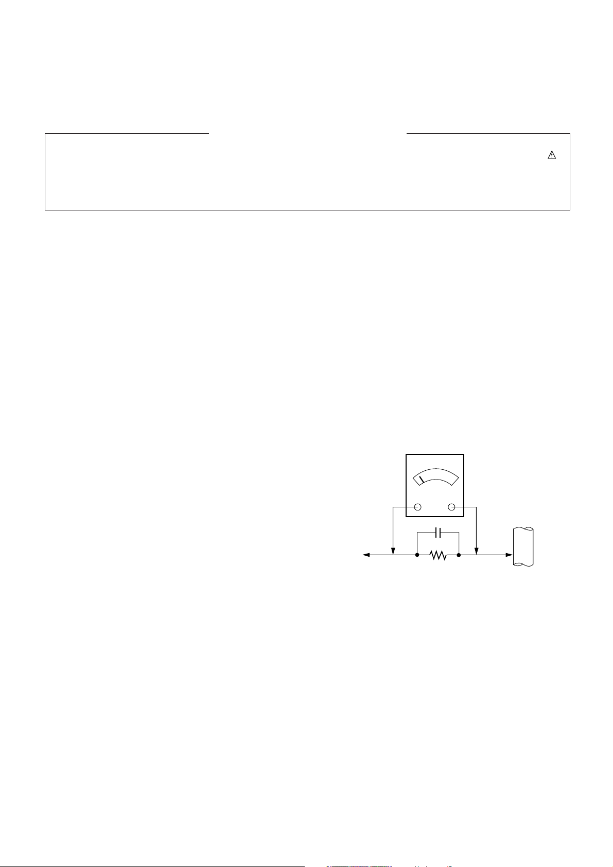
Leakage Current Hot Check (See below Figure)
Plug the AC cord directly into the AC outlet.
Do not use a line Isolation Transformer during this check.
Connect 1.5K/10watt resistor in parallel with a 0.15uF capacitor
between a known good earth ground (Water Pipe, Conduit, etc.)
and the exposed metallic parts.
Measure the AC voltage across the resistor using AC
voltmeter with 1000 ohms/volt or more sensitivity.
Reverse plug the AC cord into the AC outlet and repeat AC
voltage measurements for each exposed metallic part. Any
voltage measured must not exceed 0.75 volt RMS which is
corresponds to 0.5mA.
In case any measurement is out of the limits specified, there is
possibility of shock hazard and the set must be checked and
repaired before it is returned to the customer.
Leakage Current Hot Check circuit
1.5 Kohm/10W
To Instrument's
exposed
METALLIC PARTS
Good Earth Ground
such as WATER PIPE,
CONDUIT etc.
AC Volt-meter
IMPORTANT SAFETY NOTICE
0.15uF
Page 4
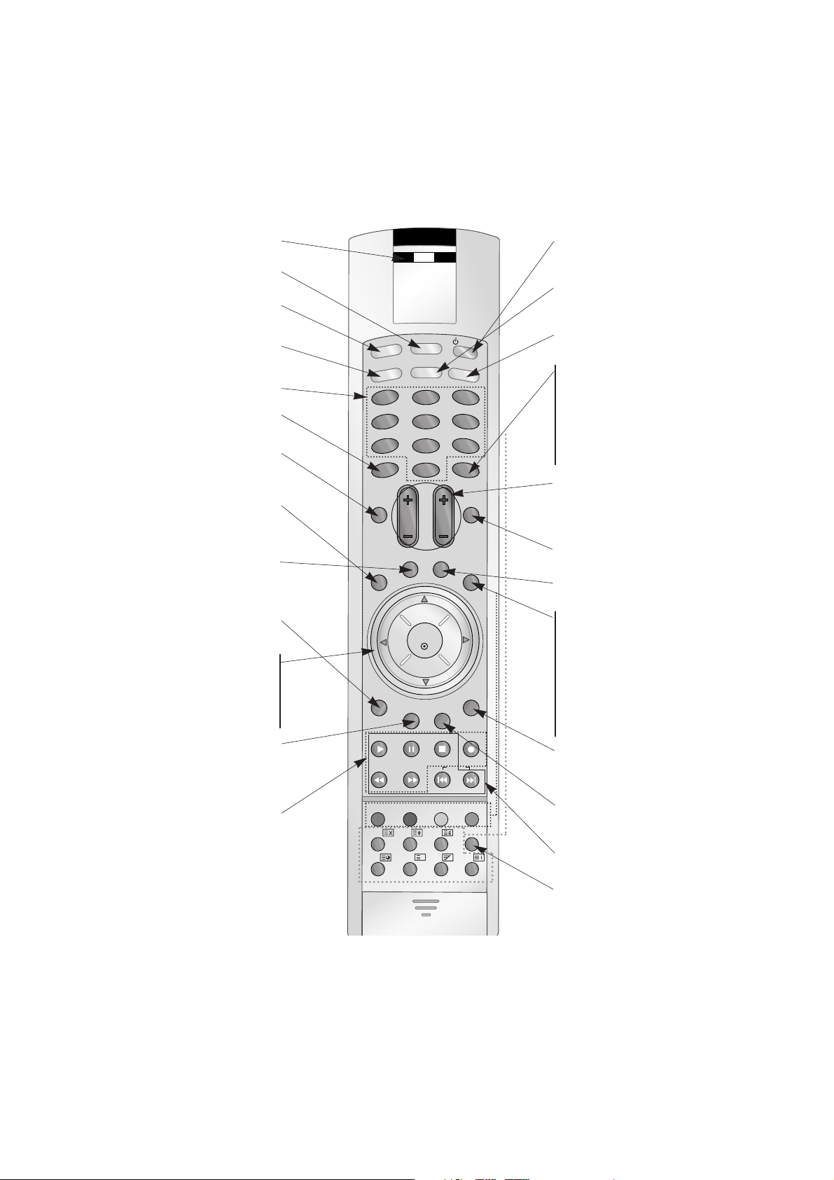
- When using the remote control aim it at the remote control sensor of the set.
- There's maybe a defect in consecutive operation of remote control in specified brightness according to this set feature.
123
456
789
0
DVD
HDSTB
AUDIO
MODE
POW
ER
A
R
C
D
/A
T
V
TV/AV
MULTIMEDIA
FAVOURITE
TEXT
MUTE
SLEEP
GUIDE
MENU
PIP PR-
TIME
PLAY
REW FF SKIP
PAUSE STOP
RECORD
MIX
INDEX
REVEAL
PIP INPUT
I/II
UPDATE
SIZE
STILL
PIP PR+
SWAP
EXIT
PSM SSM
OK
INFO
PIP
PR
VOL
CABLE
VCR
?
TV
LIST
displays the selected device.
D/A TV
selects analogue or digital mode.
MODE
selects another device.
NUMBER buttons
INFO
displays information on top of the
screen during watching the TV.
(In Digital mode only)
OK
accepts your selection or displays
the current mode.
DD/ EE
or FF/
GG
adjusts menu settings.
selects menu item.
POWER
switches the set on from standby or
off to standby.
MULTIMEDIA
selects Component 1/2, RGB-DTV,
RGB-PC, DVI-DTV or DVI-PC modes.
switches the set on from standby.
ARC (Aspect Ratio Control)
changes the picture format.
TEXT
These buttons are used for teletext.
For further details, see the ‘Teletext’
section.
switches the subtitle on or off in Digital
mode.
Note : In teletext mode, the PIP PR +/-,
SWAP and PIP INPUT buttons are used
for teletext function.
VOL +/- (Volume Up/Down)
increases/decreases sound level.
PR +/- (Programme Up/Down)
selects a programme.
switches the set on from standby.
FAVOURITE
selects a favourite programme.
LIST
displays the programme table.
PIP
switches the sub picture on or off.
PIP PR +/-
selects a programme for the sub picture.
SWAP
alternates between main and sub
picture.
PIP INPUT
selects the input mode for the sub
picture.
EXIT
clears all on-screen displays and
returns to TV viewing from any
menu.
SSM (Sound Status Memory)
recalls your preferred sound setting.
DVD BUTTONS
controls a LG DVD player.
I/II
selects the sound output or the audio
mode.
TV/AV
selects the remote operating mode.
switches the set on from standby.
SLEEP
sets the sleep timer.
MUTE
switches the sound on or off.
GUIDE
shows a programme schedule.
(In Digital mode only)
VCR BUTTONS
controls a LG video cassette
recorder.
PSM (Picture Status Memory)
recalls your preferred picture setting.
MENU
selects a menu.
- 4 -
DESCRIPTION OF CONTROLS
Page 5

- 5 -
<Front Panel Controls>
TV/AVON/OFF MENU VOL PR
Main Power Button
Remote Control Sensor
TV/AV Button
selects the TV, AV, Component,
RGB or DVI modes. If OSD is dis-
played, selects menu item.
switches the set on from standby.
MENU
displays on screen menus one by one.
exits the current menu.
memorizes menu changes.
DD/ EE
(Programme Up/Down)
selects a programme or a menu item.
switches the set on from standby.
FF/ GG
(Volume Up/Down)
adjusts the volume.
adjusts menu settings.
Power Standby Indicator
Illuminates red in standby
mode, Illuminates green
when the set is turned on
Page 6
- 6 -
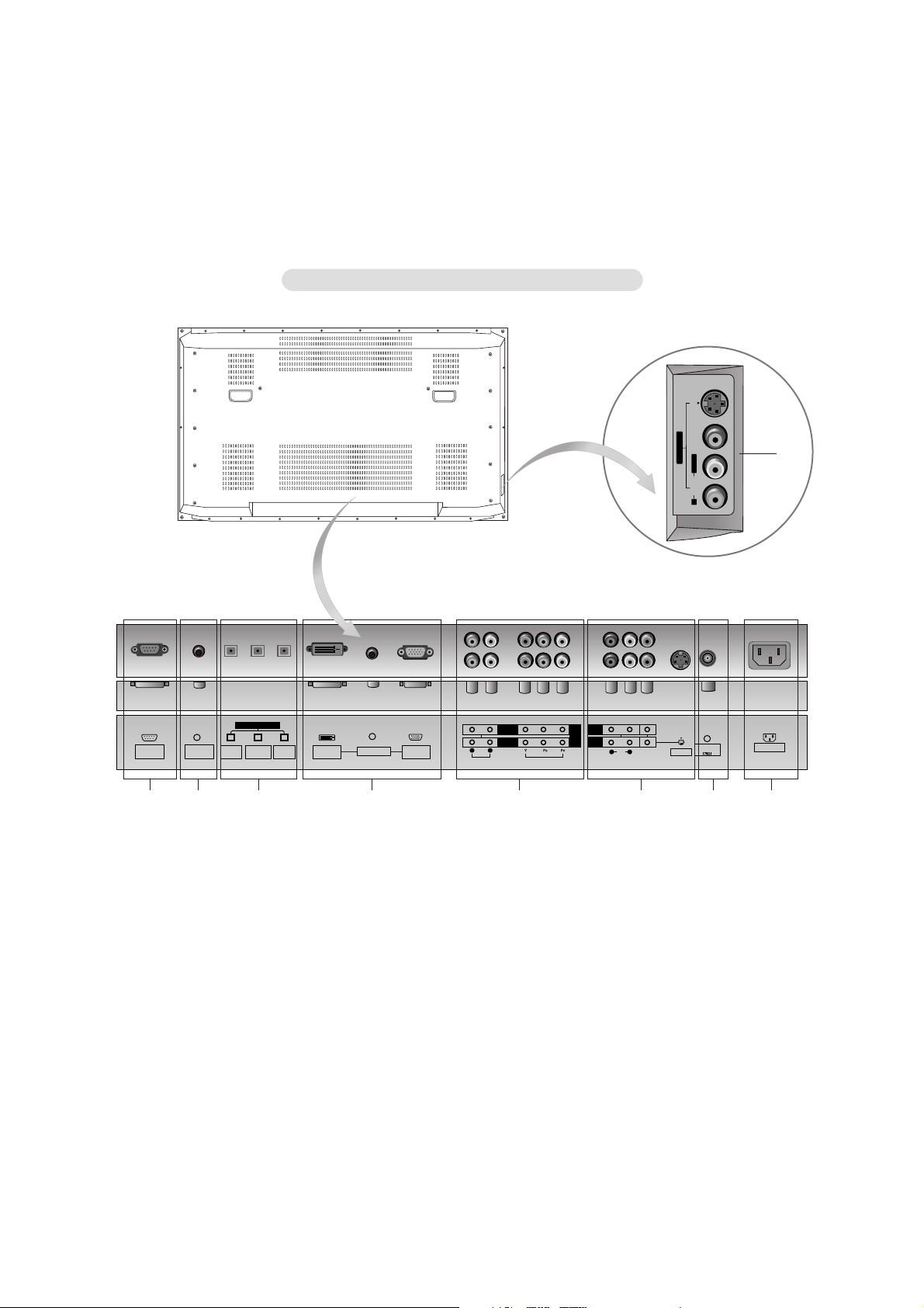
<Back Panel>
1. UPGRADE PORT
This port is used to upgrade the software version and debug
without changing the hardware.
Be careful not to use this port. Just contact your dealer or service centre.
2. CONTROL LOCK / REMOTE CONTROL
3. DVI INPUT/COMPONENT 1 INPUT/OUTPUT (DIGITAL
AUDIO (OPTICAL))
Connect digital audio from various types of equipment.
Note: In standby mode, these ports will not work.
4. DVI INPUT / AUDIO INPUT / RGB INPUT (PC/DTV)
Connect the monitor output socket of the PERSONAL COMPUTER to this socket.
Note: If you want to use RGB/DVI audio, we strongly recommend that you use the cable that has a core, or the EMI Filter
core along with separate cable.
5. COMPONENT INPUT
Connect DVD video outputs to Y, PB, PR of COMPONENT
INPUT and audio outputs to Audio sockets of AUDIO INPUT.
6. AUDIO/VIDEO IN SOCKETS (A/V INPUT 1)
Connect the audio/video out sockets of external equipment to
these sockets.
S-VIDEO/AUDIO IN SOCKETS
Connect the S-VIDEO out socket of the VCR to the S-VIDEO
socket.
Connect the audio out sockets of the VCR to the audio sockets as in A/V INPUT 1.
AUDIO/VIDEO OUT SOCKETS (MONITOR OUTPUT)
7. ANTENNA INPUT
8. POWER CORD SOCKET
This Monitor operates on an AC power. The voltage is indicated on the Specifications page. Never attempt to operate
the Monitor on DC power.
9. AUDIO/VIDEO IN SOCKETS (A/V INPUT 2)
S-VIDEO/AUDIO IN SOCKETS
9
S-VIDEOVIDEOAUDIO
A/V INPUT 2
R
L/MONO
4 5 6 7 81 2 3
- Shown is a simplified representation of the set.
- Here shown may be somewhat different from your set.
- This manual explains the features available on the DT-50PY10 series.
DIGITAL AUDIO (OPTICAL)
PORT
REMOTE
CONTROL
INPUT
DVI
COMPONENT 1
INPUT
OUTPUT
DVI INPUT
(PC/DTV)
UPGRADE
AUDIO INPUT
MONITOR
RGB INPUT
(PC/DTV)
COMPONENT 2
COMPONENT 1
R L
AUDIO INPUT VIDEO INPUT
INPUT
DVD
OUTPUT
.
DTV
A/V
INPUT 1
R L
AUDIO
VIDEO
S-VIDEO
Antenna
ANALOG/DTV
AC INPUT
Page 7
- 7 -
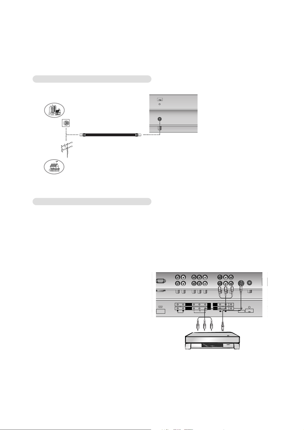
- Be careful for the bronze wire not to be bended in connecting to antenna input port.
Antenna Connection
Watching VCR
- When connecting the Monitor to external equipment, match the colours of connecting ports (Video - yellow, Audio (L) - white,
Audio (R) -red).
- Connect the VIDEO OUTPUT socket (yellow) to the VIDEO INPUT on the set.
- If you have a mono VCR, connect the audio cable from the VCR to the AUDIO (L/MONO) input on the set.
- If you connect an S-VIDEO VCR to the S-VIDEO input, the picture quality is improved; compared to connecting a regular VCR
to the Video input.
- Use the orbiter function to Avoid having a fixed image remain on the screen for a long period of time. Typically a frozen still picture from a VCR. (Refer to p. 28)
If a 4:3 picture format is used; the fixed image may remain visible on the screen.
- To avoid picture noise (interference), leave an adequate distance between the VCR and the set.
Watching TV programmes
- Turn the set on and select the programme you
want.
Watching VCR
1. Use the TV/AV button on the remote control to
select VIDEO 1 or VIDEO 2.
- If both S-VIDEO and VIDEO sockets have been
connected to the S-VHS VCR simultaneously, only
the S-VIDEO can be received.
2. Insert a video tape into the VCR and press the
PLAY button on the VCR.
(See VCR owner’s manual)
RGB INPUT
(PC/DTV)
S-VIDEO
MONITOR
OUTPUT
A/V
INPUT 1
Antenna
ANALOG/DTV
AUDIO INPUT VIDEO INPUT
AUDIO
VIDEO
COMPONENT 2
DVD
DTV
INPUT
.
COMPONENT 1
R L
R L
AC
< Back panel of the set >
< VCR >
YPB PR LR
L
(MONO)
R
COMPONENT
S-VIDEO VIDEO AUDIO
AUDIO
AV4
Antenna
REMOTE
CONTROL
RS-232C INPUT DVI INPUT
(CONTROL/SERVICE)
AUDIO INPUT RGB INPUT
Apartments
(connecting to wall antenna socket)
Private house
(connecting to wall outdoor antenna)
outdoor antenna
wall antenna socket
VHF antenna
UHF antenna
RF coaxial wire (75 ohms)
< Back panel of the set >
Page 8
- 8 -
Watching Cable TV
- After subscribing for a local cable TV station and installing a converter you can watch cable TV.
- For further information of cable TV, contact the local cable TV station.
To watch cable TV
1. Use the TV/AV button on the remote control to
select VIDEO 1 or VIDEO 2.
2. Tune to cable service provided channels using
the cable box.
RGB INPUT
(PC/DTV)
S-VIDEO
MONITOR
OUTPUT
A/V
INPUT 1
Antenna
ANALOG/DTV
AUDIO INPUT VIDEO INPUT
AUDIO
VIDEO
COMPONENT 2
DVD
DTV
INPUT
.
COMPONENT 1
R L
R L
AC I
< Back panel of the set >
< Cable box >
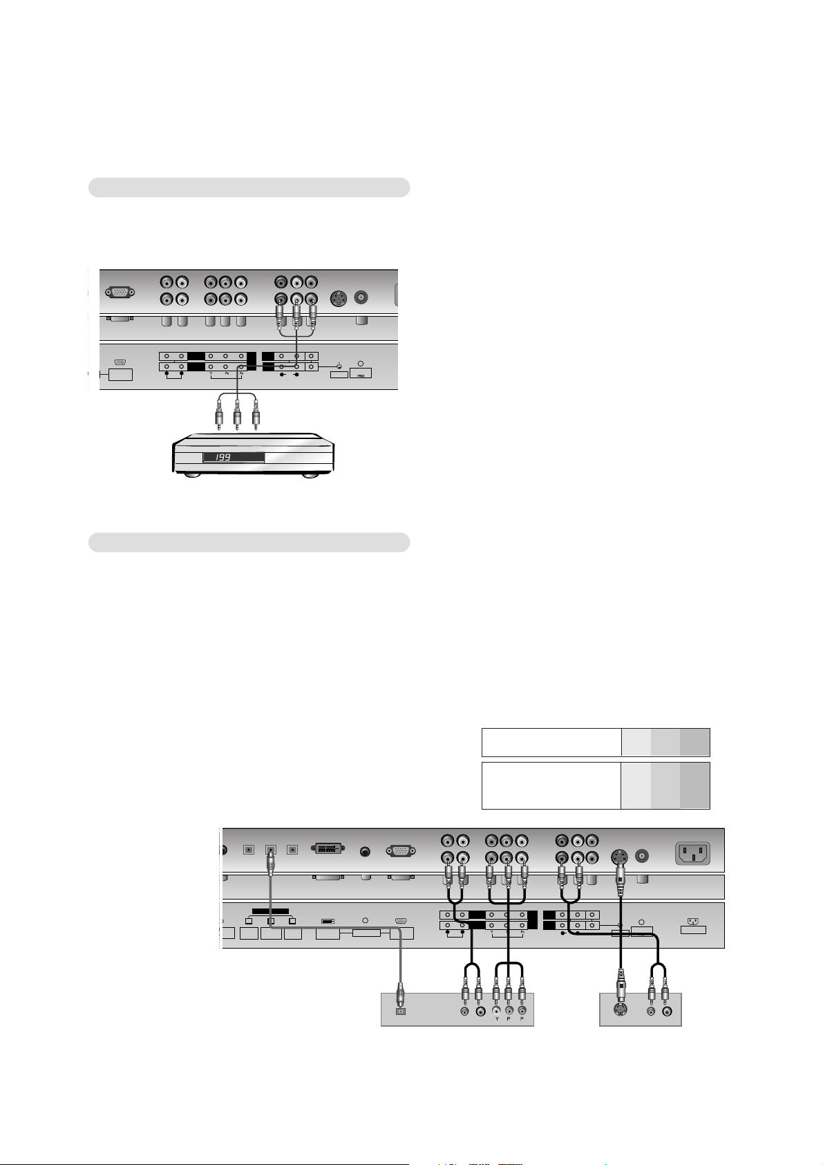
Watching DVD
How to use
1. Turn on the DVD player, insert a DVD.
2. Use the TV/AV or MULTIMEDIA button on the remote control to select
Component 1 or Component 2.
(If connected to S-VIDEO, select the VIDEO 1 or VIDEO 2 external input
source.)
3. Refer to the DVD player's manual for operating instructions.
How to connect
1. Connect the DVD video outputs (Y, PB, PR) to the COMPONENT (Y, PB, PR) INPUT jacks on the set and connect the DVD
audio outputs to the AUDIO INPUT jacks on the set, as shown in the figure.
2. If your DVD only has an S-Video output jack, connect this to the S-VIDEO input on the set and connect the DVD audio outputs
to the AUDIO INPUT jacks on the set, as shown in the figure.
Note:
a. If your DVD player does not have component video output, use S-Video.
b. Digital Audio will not work for Component 2 input source. Digital Audio operation has priority if Digital Audio and AUDIO L/R
are connected at the same time.
• Component Input ports
You can get better picture quality if you connect
DVD player with component input ports as below.
Component ports of the
set
Y
P
B
PR
Video output ports
of DVD player
Y
Y
Y
Y
Pb
B-Y
Cb
PB
Pr
R-Y
Cr
P
R
< Back panel of the set >
< DVD player >
or
or
DIGITAL AUDIO (OPTICAL)
TROL
OTE
DVI
COMPONENT 1
INPUT
INPUT
OUTPUT
DVI INPUT
(PC/DTV)
AUDIO INPUT
RGB INPUT
(PC/DTV)
COMPONENT 2
COMPONENT 1
R L
AUDIO INPUT VIDEO INPUT
DVD
.
DTV
INPUT
MONITOR
OUTPUT
A/V
INPUT 1
R L
AUDIO
VIDEO
Antenna
ANALOG/DTV
S-VIDEO
AC INPUT
DIGITAL AUDIO
OPTICAL
(R) AUDIO (L)
B
R
S-VIDEO
(R) AUDIO (L)
Page 9
- 9 -
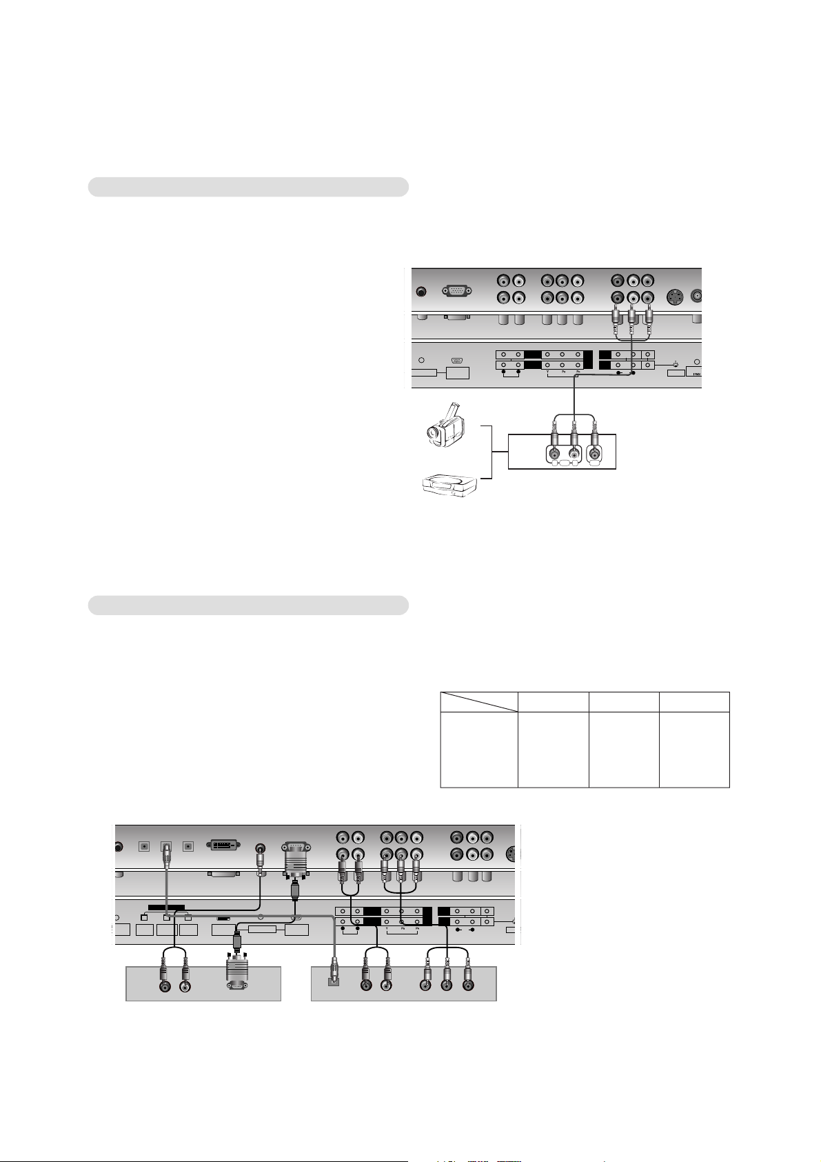
Watching external AV source
- When connecting the set to an external source, match the colours of AUDIO/VIDEO input jacks on the set with the output jacks
on the audio/video equipment: Video = yellow, Audio (Left) = white, Audio (Right) = red.
How to use
1. Use the TV/AV button on the remote control to
select VIDEO 1 or VIDEO 2.
2. Operate the corresponding external equipment.
See external equipment operating guide.
RGB INPUT
(PC/DTV)
S-VIDEO
MONITOR
OUTPUT
A/V
INPUT 1
Antenna
ANALOG/DTV
AUDIO INPUT VIDEO INPUT
AUDIO
VIDEO
AUDIO INPUT
COMPONENT 2
DVD
DTV
INPUT
.
COMPONENT 1
R L
R L
RL
AUDIO VIDEO
< Back panel of the set >
Camcorder
Video game set
Watching DTV
How to connect
1. Use the monitor’s COMPONENT (Y, PB, PR) INPUT, RGB or DVI
jack for video connections, depending on your set-top box connector. Then, make the corresponding audio connections.
How to use
1. Turn on the digital set-top box. (Refer to the owner’s manual for
the digital set-top box.)
2. Use TV/AV or MULTIMEDIA on the remote control to select
Component 1, Component 2, RGB-DTV or DVI-DTV.
- This set can receive Digital Over-the-air/Cable signals without an external digital set-top box. However, if you do
receive Digital signals from a digital set-top box or other digital external device, refer to the figure as shown below.
(R) AUDIO (L) YP
BR
P
DIGITAL AUDIO
OPTICAL
DVI
INPUT
COMPONENT 1
INPUT
OUTPUT
DVI INPUT
(PC/DTV)
RGB INPUT
(PC/DTV)
S-VIDEO
MONITOR
OUTPUT
A/V
INPUT 1
AUDIO INPUT VIDEO INPUT
AUDIO
VIDEO
AUDIO INPUT
DIGITAL AUDIO (OPTICAL)
COMPONENT 2
DVD
DTV
INPUT
.
COMPONENT 1
R L
R L
(R) AUDIO (L)
DTV OUTPUT
R
R
R
R
R
< Back panel of the set >
< Digital Set-top Box >
• DTV Input signal
480i / 576i
480p / 576p
720p (50/60Hz)
1080i (50/60Hz)
Mode
Terminal
Component
o
o
o
o
RGB
x
o
o
o
DVI
x
o
o
o
or
or
Page 10
- 10 -
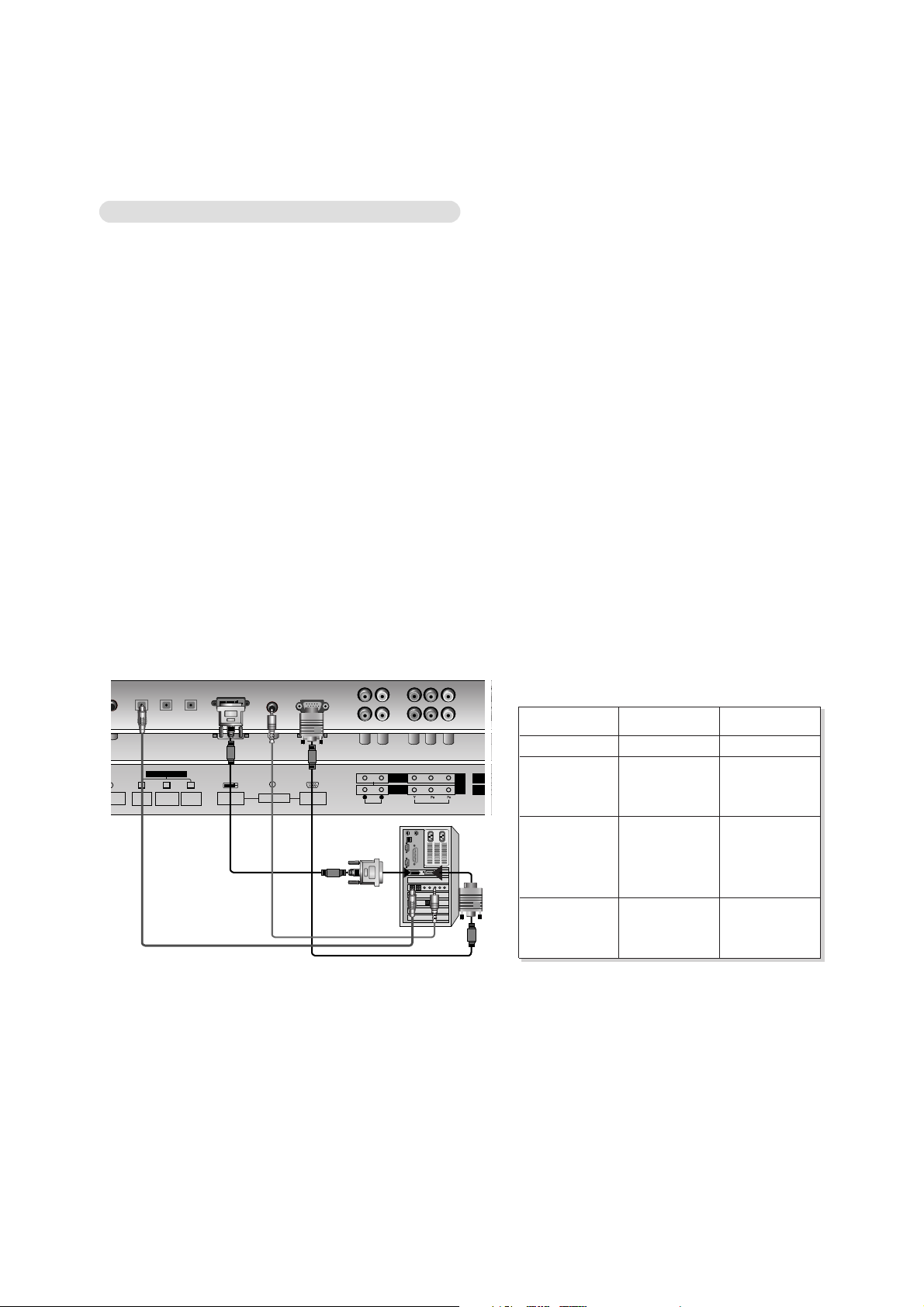
Connecting PC
How to connect
1. To get the best picture quality, adjust the PC graphics card to 1024x768, 60Hz.
2. Use the set’s RGB INPUT or DVI (Digital Visual Interface) INPUT port for video connections, depending on your PC connector.
If the graphic card on the PC does not output RGB and DVI simultaneously, connect only one of either RGB INPUT or DVI
INPUT to display the PC on the set.
3. Then, make the corresponding audio connections. If using a sound card, adjust the PC sound as required.
How to use
1. Turn on the PC and apply power to the set.
2. Press the MENU button and then
DD / EE
button to select the SPECIAL menu.
3. Press the GGbutton and then
DD / EE
button to select Main input.
4. Press the GGbutton and then
DD / EE
button to select RGB-PC, RGB-DTV, DVI-PC or DVI-DTV.
PC screen appears on the set.
The set can be operated as the PC monitor.
5. Check the image on your set. There may be noise associated with the resolution, vertical pattern, contrast or brightness in PC
mode. If noise is present, change the PC mode to another resolution, change the refresh rate to another rate or adjust the brightness and contrast on the menu until the picture is clear. If the refresh rate of the PC graphic card can not be changed, change
the PC graphic card or consult the manufacturer of the PC graphic card.
Note:
a. Depending on the graphics card, DOS mode may not work if you use a DVI-D cable.
b. Avoid keeping a fixed image on the TV's screen for a long period of time. The fixed image may become permanently imprinted
on the screen.
c. The synchronization input form for Horizontal and Vertical frequencies is separate.
MOTE
DVI
INPUT
COMPONENT 1
INPUT
OUTPUT
DVI INPUT
(PC/DTV)
RGB INPUT
(PC/DTV)
MONITOR
OUTPUT
A/V
INPUT 1
AUDIO INPUT VIDEO INPUT
AUDIO INPUT
DIGITAL AUDIO (OPTICAL)
COMPONENT 2
DVD
DTV
INPUT
.
COMPONENT 1
R L
< Back panel of the set >
RGB PC / DVI PC mode
Displayable Monitor Specification
Resolution
640x350
640x480
800x600
Horizontal
Frequency(KHz)
Vertical
Frequency(Hz)
1024x768
70.09
59.94
72.80
75.00
56.25
60.31
72.18
75.00
60.00
70.06
75.02
31.468
31.469
37.861
37.500
35.156
37.879
48.077
46.875
48.363
56.476
60.023
or
Page 11
- 11 -
1. Press the OK button and then
DD / EE
button to select the desired picture item.
2. Press the GGbutton and then
FF / GG
or
DD / EE
button to make appropriate adjust-
ments.
Position
This function is to adjust picture to left/right and up/down as you prefer.
Phase & Clock (RGB-PC mode only)
This function allows you to remove any horizontal noise and clear or sharpen the
image of characters.
To correct the screen size, adjust Clock.
• The adjustment range of Phase is 0 ~ 31.
• The adjustment range of Clock is 0 ~ 32.
Note : Some signal from some graphics boards may not function properly. If the results are unsatisfactory, adjust your monitor’s position, size and phase manually.
Reset
This function allows you to return to the good picture reproduction programmed at the factory and cannot be changed.
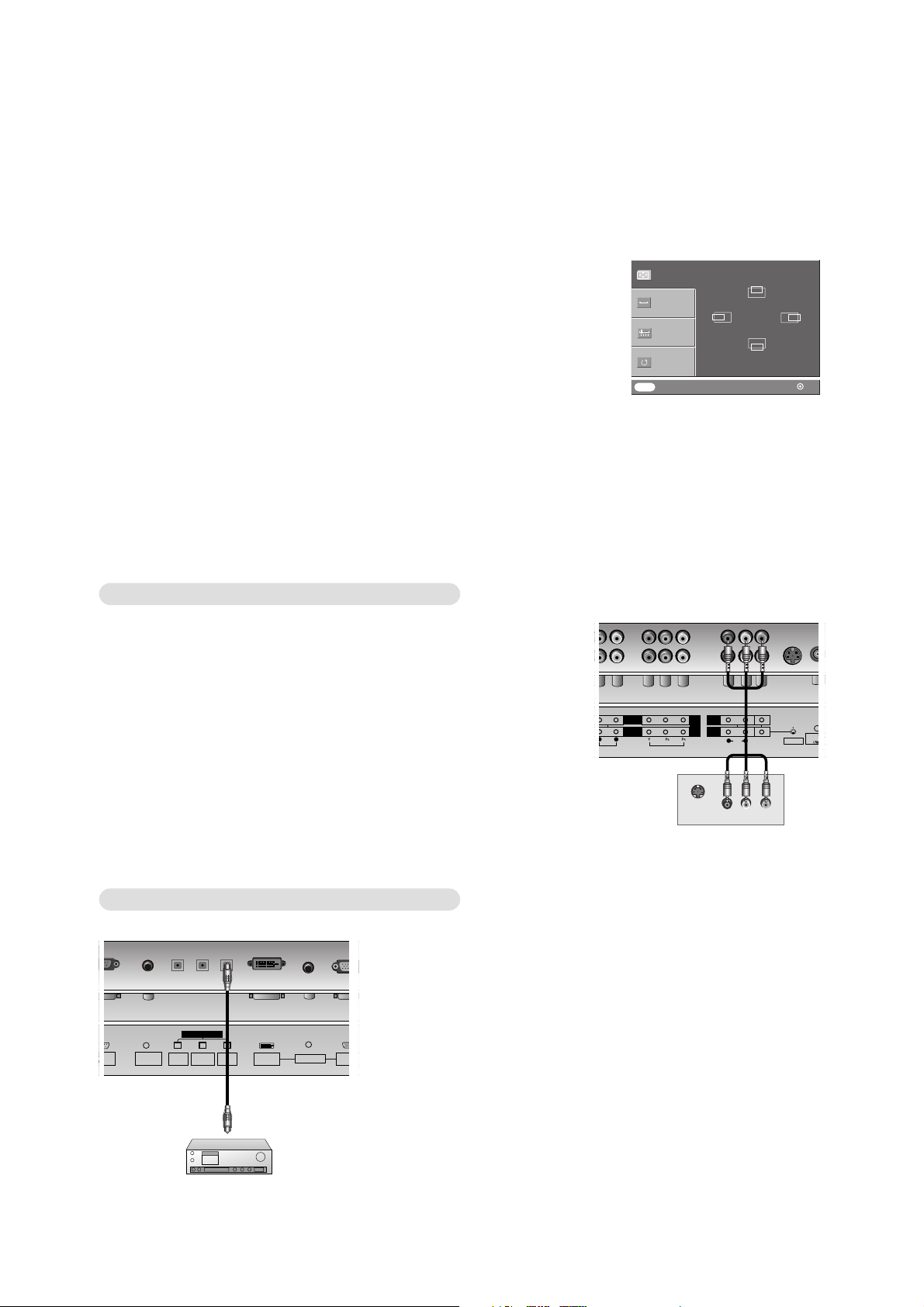
Screen Adjustments
- This function works in the following mode:
Component 1, Component 2, RGB-PC, RGB-DTV or DVI-DTV
Close Move OK
POSITION
GG
CLOCK
PHASE
RESET
DD
FF GG
EE
DD
EE
MENU
- Send the set’s audio to external audio equipment (stereo system) via the
Digital Audio Output (Optical) port.
Caution: Do not look into the optical output port. Looking at the laser
beam may damage your vision.
Digital Audio Output
How to connect
1. Connect one end of an optical cable to the TV Digital Audio (Optical)
Output port.
2. Connect the other end of the optical cable to the digital audio (optical)
input on the audio equipment.
3. Set the “ TV Speaker option - Off” in the AUDIO menu. Refer to page
23.
See the external audio equipment instruction manual for operation.
REMOTE
CONTROL
DVI
INPUT
COMPONENT 1
INPUT
OUTPUT
DVI INPUT
(PC/DTV)
RGB INPU
(PC/DTV)
AUDIO INPUT
DIGITAL AUDIO (OPTICAL)
< Back panel of the set >
- The set has a special signal output capability which allows you to hook up a second TV or monitor.
Connect the second TV or monitor to the set’s MONITOR OUTPUT. See the
Operating Manual of the second TV or monitor for further details regarding that
device’s input settings.
Note: DTV, Component, RGB-PC/RGB-DTV, DVI-PC/DVI-DTV input sources cannot
be used for Monitor out.
Monitor Out Setup
S-VIDEO
MONITOR
OUTPUT
A/V
INPUT 1
Antenna
ANALOG/DT
AUDIO INPUT VIDEO INPUT
AUDIO
VIDEO
COMPONENT 2
DVD
DTV
INPUT
.
COMPONENT 1
R L
R L
S-VIDEO
IN
(R) AUDIO (L) VIDEO
< Back panel of the set >
Page 12
- 12 -
A
S
m
a
r
k
LG TV
Owner’s Manual
1.5V
1.5V
Alkaline batteries
Power Cord
123
456
789
0
DVD
STB
AUDIO
MODE
P
O
W
E
R
M
U
T
E
T
V
/
A
V
M
U
L
T
IM
E
D
IA
ARC
SSM
Q.VIEW
PSM
FAVOURITE
MENU
PIP PR-
REVEAL
LIST
PLAY
REW FF SKIP
PAUSE STOP
RECORD
SPLIT ZOOM
SLEEP
I/II
WIN.SIZE
WIN.POSITION
PIP INPUT
PIP PR+ SWAP
OK
PIP/DW
EXIT
PR
VOL
CABLE
VCR
?
TV
TEXT/
Remote Control handset
- Optional extras can be changed or modified for quality improvement without any notification new optional extras can be
added.
- Contract your dealer for buying these items.
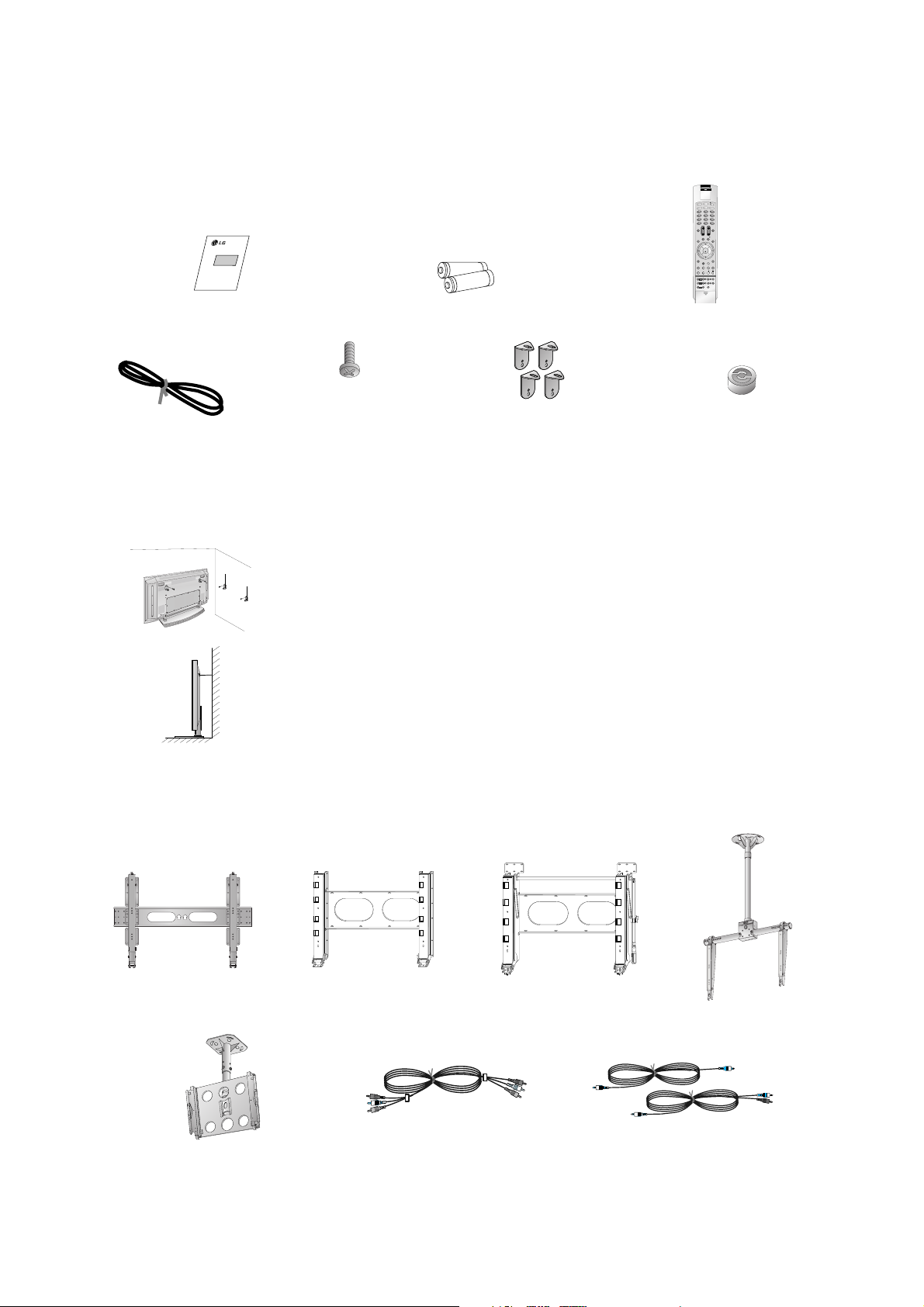
Optional Extras
Accessories
Accessories
Video cables
Audio cables
6-RING SPACER
(Only DT-60PY10 series)
2-TV bracket bolts
(or DT-50PY10 series: 4-TV
bracket bolts)
(Only DT-60PY10 series : 6-Wall
mounting bracket bolts)
Ceiling mounting bracket
Wall mounting bracket
(Only DT-60PY10 series)
Tilt wall mounting bracket
(Only DT-60PY10 series)
Tilt wall mounting bracket
404250 40 42 50
Ceiling mounting bracket
4
0
4
2
5
0
42
40
2-TV brackets
2-Wall brackets (option)
- Secure the TV assembly by joinning it to a wall by using the TV/Wall brackets.
Joinning the TV assembly to the wall to protect the set tumbling
• After the set must be mounted on s desk top, install the TV brackets on the TV as shown.
Insert the 2 bolts and tighten securely, in the holes on the bracket.
(Only DT-50PY10 series: After removing the existing bolts, insert the 4 bolts and tighten securely, in the holes on the bracket.)
Install the wall brackets on the wall with 4 bolts, (not supplied with the product), as shown.
Match the height of the TV brackets and the wall brackets.
Check to be sure the brackets are tightened securely.
• Secure the TV assembly to the wall with strong strings or wound wire cables, (not supplied
with the product), as shown.
Page 13

Maker : SONY(42 inch)
SONY/Sanken(50 inch)
LG(60 inch)
RGB Closed Type
Maker : LG Chemical
- 13 -
SPECIFICATIONS
NOTE : Specifications and others are subject to change without notice for improvement
.
PAL-B/G, DTV : DVB-T
VHF : 00~12
UHF : 28~69
CATV : 02~44
PAL : 38.90MHz
DVB-T : 36.167MHz
240V~, 50Hz
PDP42X2xxxx
PDP50X2xxxx
PDP60X5xxxx
16:9
45% Total light transmittance(E-Mesh)
0 40 deg
85 %
-20 60 deg
85 %
1
2
3
4
5
6
7
8
9
10
11
Broadcasting system
Available Channel
Tuner IF
Input Voltage
PDP Module
Aspect ratio
Screen Filter
Operating Temperature
Operating Humidity
Storage Temperature
Storage Humidity
V General Specification
Specification
MIN Typ Max Unit
No Item Remark
V Application Range
This spec is applied to the 42”, 50”, 60”PDP TV used AF-046A
Chassis.
V Specification
Each part is tested as below without special appointment.
1) Temperature : 25±5°C (77±9°F)
2) Relative Humidity: 65±10%
3) Power Voltage: Standard Input voltage (100-240V~, 50/60Hz)
* Standard Voltage of each product is marked by models.
4) Specification and performance of each parts are followed
each drawing and specification by part number in accordance
with BOM.
5)
The receiver must be operated for about 20 minutes prior to the
adjustment
.
V Test and Inspection Method
1) Performance : LGE TV test method followed.
2) Demanded other specification
Safety: CB specification
EMC : CISPR 13 specification
Remark
Safety : IEC60065, EN60065
EMC : CISPR13 Class B
Model Name
DT-42PY10X
DT-50PY10
DT-60PY10
Market
Australia
Page 14
- 14 -
1. Application Object
These instructions are applied to all of the PDP TV, AF-046A.
2. Notes
(1) Because this is not a hot chassis, it is not necessary to use
an isolation transformer. However, the use of isolation
transformer will help protect test equipment.
(2) Adjustments must be done in the correct order.
(3) The adjustments must be performed in the circumstance of
25±5°C of temperature and 65±10% of relative humidity if
there is no specific designation.
(4) The input voltage of the receiver be must kept 220V, 60Hz
when adjusting.
(5) The receiver must be operational for about 15 minutes
prior to the adjustments.
O After receiving 100% white pattern, the receiver must be
operate prior to adjustment.(Or white condition in HEATRUN mode)
O Enter into HEAT-RUN MODE
- Press the POWER ON KEY on R/C for adjustment.
OSD display and screen display 100% full WHITE
PATTERN.
[ Set is activated HEAT-RUN without signal generator in
this mode.
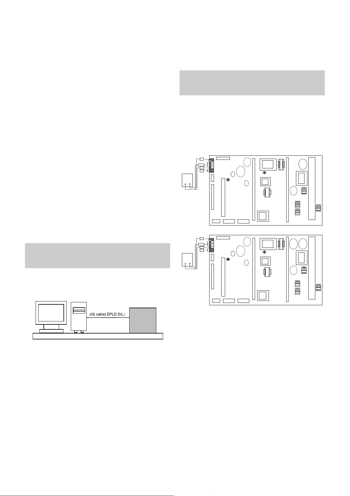
3. EPLD Download
(1) Test Equipment: PC, Jig for download
(2) Connect the power of VSC B/D.
(3) Execute download program of PC.
(4) After executing the hot key on the Programmer, click icon
(5) End after confirming.
4. POWER PCB Assy Voltage
Adjustment
(Va, Vs Voltage Adjustment)
4-1. Test Equipment : D.M.M 1EA
4-2. Connection Diagram for Measuring
Refer to Fig 1.
(1) Va Adjustment
1) After receiving 100% Full White Pattern, Heat-Run(over
10min).
2) Connect + terminal of D.M.M to Va pin of P805 and
connect – terminal to GND pin of P805.
3) Adjust RV601 voltage to match that of the label on the
Top/Right of the panel. (Deviation : ±0.5V)
(2) Vs Adjustment
1) Connect + terminal of D.M.M to Vs pin of P805 and
connect – terminal to GND pin of P805.
2) Adjust RV401 voltage to match that of the label on the
Top/Right of the panel. (Deviation : ±0.5V)
If you turn on a still screen more than 20 minutes (Especially
Digital pattern(13 CH), Cross Hatch Pattern), an afterimage
may occur in the black level part of the screen.
ADJUSTMENT INSTRUCTIONS
PC
VSC
B/D
<Fig 1> Connection Diagram of EPLD Download
Each PCB Assy must be checked by Check JIG Set before
assembly. (Especially, be careful Power PCB Assy which can
cause Damage to the PDP Module.)
Va ADJ
RV601
P806
P805
P807
Va
GND
NC
VS
DMM
+-
P804
P801
P802
Vs ADJ
V401
P803
Va ADJ
RV601
P806
P805
P807
Va
GND
NC
VS
DMM
+-
P804
P801
P802
Vs ADJ
V401
P803
<3501V00182B>
<3501V00188A>
<Fig. 2-1> Connection Diagram of Power Adjustment for
Measuring (Power Board)
Page 15
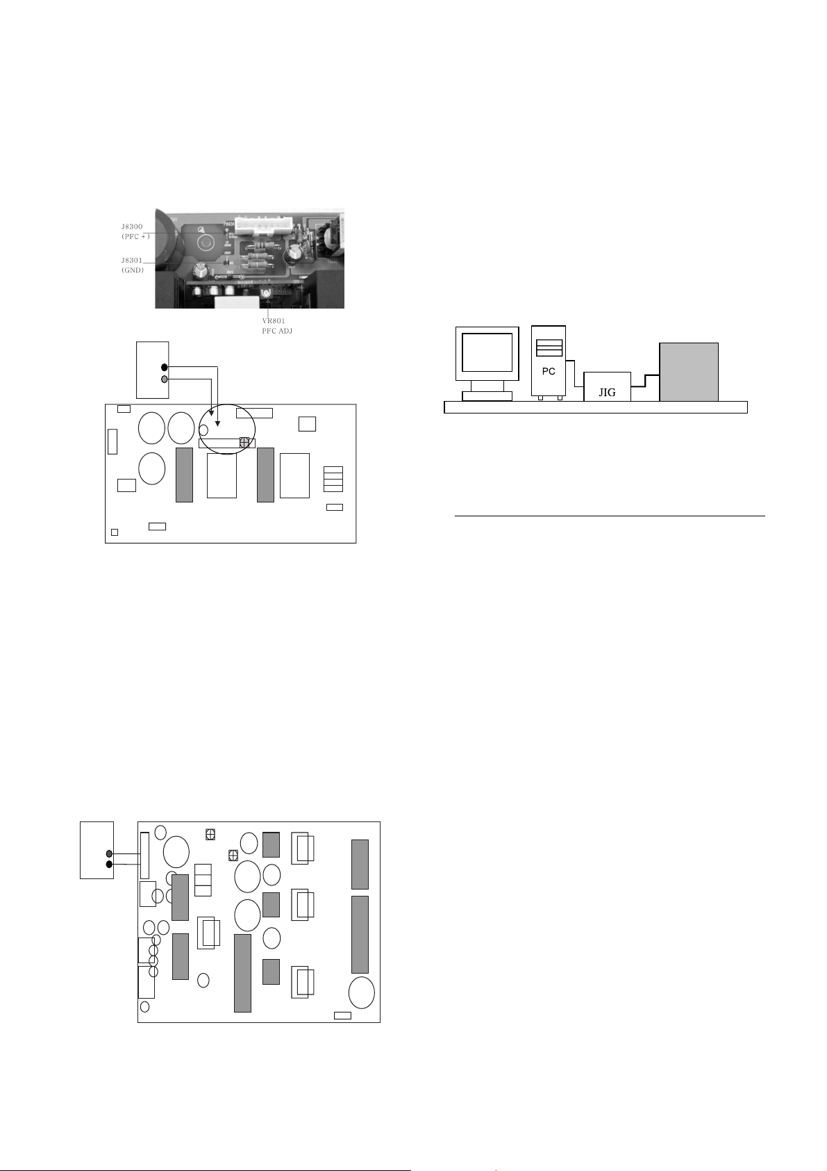
4-3. 60” Model Voltage Adjustment
1) Select 100% Full White Pattern and then Heat-Run.
2) Connect + terminal of D.M.M to RFC + terminal of J8300
and connect – terminal to GND pin of J8301.
3) Adjust V8401 voltage to match 380V(±1V)
(1) Va Adjustment
1) After receiving 100% Full White Pattern, Heat-Run(over
10min).
2) Connect + terminal of D.M.M to Va pin of P8011 and
connect – terminal to GND pin of P8011.
3) Adjust VR401 voltage to match that of the label on the
Top/Right of the panel. (Deviation : ±0.5V)
(2) Vs Adjustment
1) Connect + terminal of D.M.M to Vs pin of P8011 and
connect – terminal to GND pin of P8011.
2) Adjust VR8501 voltage to match that of the label on the
Top/Right of the panel. (Deviation : ±0.5V)
5. EDID(The Extended Display
Identification Data)/DDC
(Display Data Channel) download
This is the function that enables “Plug and Play".
5-1. Required Test Equipment
1) PC, Jig for adjusting DDC (PC serial to D-sub.
Connection equipment)
2) D-Sub to DVI Connector
5-2. Composition of Device
5-3. EDID DATA
- Download only EDID for DVI.
6. AD9883A-Set Adjustment
6-1. Synopsis
AD9883A-Set adjustment to set the black level and the Gain
of optimum with an automatic movement from the analog =>
digital converter.
6-2. Test Equipment
Service R/C, 801GF(802B, 802F, 802R) or MSPG3240A
Pattern Generator
(720P 60Hz 100% Color Bar Pattern output will be possible
and the output level will accurately have to be revised with
0.7±0.1Vp-p)
- 15 -
D
M
M
+
-
P801 1
VR8501
Vs AD J
VR8401
Va ADJ
<Fig. 2-2> Connection Diagram of Power Adjustment for
Measuring (60 “ Model PFC Board)
<Fig. 2-3> (P/N : 6871VPMA78A) Connection Diagram of
Power Adjustment for Measuring (Power Board)
DMM
VR80 1
PFC ADJ
P803A
PDP
SET
00 |
10 |
20 |
30 |
40 |
50 |
60 |
70 |
80 |
90 |
A0 |
B0 |
C0 |
D0 |
E0 |
F0 |
00
00
23
0F
01
13
3E
47
00
02
C4
96
58
00
00
00
00
01
FF
0E
4B
01
00
08
20
00
01
8E
00
2C
00
00
00
00
02
FF
01
52
01
4C
00
54
00
04
21
C4
25
00
00
00
00
03
FF
03
2F
01
6C
00
56
00
00
00
8E
00
00
00
00
00
04
FF
80
CE
01
42
00
0A
00
01
00
21
C4
00
00
00
00
05
FF
6E
00
01
00
00
20
00
1D
1E
00
8E
00
00
00
00
06
FF
3E
31
C3
00
00
20
00
00
8C
00
21
00
00
00
00
07
00
78
CA
1E
18
00
20
00
72
0A
18
00
00
00
00
00
08
1E
0A
01
00
00
00
20
00
51
D0
01
00
00
00
00
00
09
6D
31
01
20
00
00
20
00
D0
8A
1D
9E
00
00
00
00
0A
01
30
01
41
00
00
20
00
1E
20
80
00
00
00
00
00
0B
01
A5
01
00
FD
00
20
00
20
E0
18
00
00
00
00
00
0C
01
58
01
20
00
00
00
00
6E
2D
71
00
00
00
00
00
0D
01
3B
01
30
37
FC
00
00
28
10
1C
00
00
00
00
00
0E
01
B8
01
10
4E
00
00
01
55
10
16
00
00
00
00
00
0F
01
26
01
60
1E
4C
01
17
00
3E
20
00
00
00
00
BF
Page 16

- 16 -
6-3. Adjustment
(1) Input the color Bar Pattern of the 720P 60Hz Mode in the
Component INPUT and the select the Input Mode as
Component2.
(2) After receiving signal for at least 1 second, press the ADJ
Key on the Service R/C to enter the ‘Ez - Adjust’ and select
the ‘1. AD9883A-Set’.
Pressing the Vol + Key to adjust with automatic movement.
(3) When the adjustment is over, 'Adjustment completed
(Press OK)' is displayed. If the adjustment has errors,
'AD9883A-Failed! Try Again' is displayed.
(4) Readjust after confirming the case Pattern or adjustment
condition where the adjustment errors.
(5) After adjustment is complete, exit the adjustment mode by
pressing the ADJ KEY.
7. Adjustment of White Balance
7-1. Required Equipment
(1) Color analyzer (CA-100 or similar product)
(2) Automatic adjustor (with automatic adjustment hour
necessity and the RS-232C communication being possible)
(3) AV Pattern Generator
7-2. Connection Diagram of Equipment
for Measuring (Automatic Adjustment)
[[
. RS-232C Command
(Automatic Adjustment)
7-3. Adjustment of White Balance(manual)
O
Operate the Zero-calibration of the CA-100, then attach
sensor to PDP module surface when you adjust.
O
Manual adjustment is also possible by the following sequence.
(1) Enter ‘3.White-Pattern’ by pressing ADJ KEY on the
Service Remote Control.
(2) Select "Test Pattern White" using Vol +/- Key and HEAT
RUN at least 15 minutes by pressing the ENTER Key.
(3) Receive the AV 50Hz, Full size, 216 Gray window pattern
signal from AV Pattern Generator.
Input mode : DT-42PY10X : AV2
DT-50PY10 : AV1
DT-60PY10 : AV1
(4) Select the Screen Adjustment as ‘Dynamic’.
(5) After attaching sensor to center of screen, select ‘2. White-
Balance’ of ‘Ez - Adjust’ by pressing the ADJ KEY on the
Service R/C. Then enter adjustment mode by pressing the
Right KEY (
G
) .
(6) Adjust the High Light using R Gain/B Gain.
(7) Adjust using Volume +/- KEY.(G Gain: 127)
DT-42PY10X : R Offset : 50/ B Offset : 48/ B Offset: 50
DT-50PY10 : R Offset : 52/ B Offset : 45/ B Offset: 60
DT-60PY10 : R Offset : 55/ B Offset : 50/ B Offset: 55
X; 0.290±0.003
Y; 0.290±0.003
Color temperature: 9,000°K±500°K
(7) After adjustment is complete, move to Ez - Adjust screen
by pressing the ENTER(Y) KEY. Then exit the adjustment
mode by press ADJ KEY.
216 FULL WHITE
CVBS Part
PDP MONITOR
COLOR
ANALYZER
TYPE; CA-100
MSPG-2100 or
MSTG-5200
<Fig. 4> Connection Diagram of Automatic Adjustment
<Fig. 3> Adjustment Pattern : 720P 60Hz Color Bar Pattern
R Gain
G Gain
B Gain
R Cut
G Cut
B Cut
00
00
00
00
00
00
ff
ff
ff
7f
7f
7f
ja 00 XX
jb 00 XX
jc 00 XX
lj 00 XX
lk 00 XX
ll 00 XX
7f
7f(Fix.)
7f
3f(Fix.)
3f
3f
RS-232C Command
[CMD ID DATA]
MIN
CENTER
(DEFAULT)
MAX
Page 17

- 17 -
TROUBLE SHOOTING GUIDE
1. Power Board
1-1. The whole flowchart which it follows in voltage output state
Start check
Manufacture enterprise
meaning of a passage
1. Check the Power Off
condition.
Doesn't the
screen whole come
out?
It is identical
with Power Off
condition?
Yes
Yes
No
No
No
No
No
2. Check the Interface
signal condition.
Is the Interface
signal operated?
Yes
3. Check the St-by 5V
signal circuit.
Doesn't the
low pressure output
come out?
Doesn't the
St-by 5V signal
come out?
Yes
Yes
No
4. Check the 5V Monitor
signal circuit.
Doesn't the
5V Monitor signal
come out?
Yes
7. Check the VSC Vs-ON
signal
Doesn't the
high tension output
come out?
Doesn't the
VSC signal Vs-ON
come out?
Yes
Yes
High tension
output voltage Drop
it occurs?
When
remove the
Y B/D Module
Input Connector, output
voltage Drop
it occurs?
When remove
the Y, Z B/D Module
Input Connector, Power
Board high tension output
voltage Drop
it occurs?
Yes No No
9. Check the Power
Board Output high
tension circuit
Yes
10. Check the Z B/D
Module Coutput circuit
Yes
When
remove the
Z B/D Module
Input Connector, output
voltage Drop
it occurs?
11. Check the Y B/D
Module Coutput circuit
Yes
No
8. Check the Vs, Va
voltage output circuit.
Doesn't the
Vs, Va voltage output
come out?
Yes
No
No
5. Check the VSC RL-ON
signal.
Doesn't the
VSC signal RL-ON
come out?
Yes
6. Check the VSC low
pressure output
Doesn't the
VSC low pressure
output come out?
Yes
Page 18

- 18 -
1-2. DT-42PY10X Sony Power Board Structure
1 2 3
T502: Vs Trans
T702: Va Trans
T101: St-by Trans
T103: Low Voltage Trans
Page 19

- 19 -
1-3. DT-50PY10 Sony Power Board Structure
1 2 3
T502 : Vs Trans
T702 : Va Trans
T101 : St-by Trans
T103 : Low Voltage Trans
Page 20

- 20 -
1-3. DT-50PY10 Sanken Power Board Structure
1 2 3
T221 : Vs Trans
T271 : Va Trans
T121 : St-by Trans
T201 : Low Voltage Trans
Page 21

- 21 -
1-4. DT-60PY10 Power Board Structure
1 2 3
AC-IN
Page 22

- 22 -
1 2 3
PFC
Page 23

- 23 -
1 2 3
DC-DC
Page 24

- 24 -
2. No Power
(1) Symptom
Ø Does’t minute discharge at module.
Ø Non does not come in into the front LED.
(2) Check follow
Is plug in power cord? Plug in power cord.
Yes
No
Is connected the Line Filter and
Power Switch Cable?
Connect the Cable.
Yes
No
Is connected the Power Switch and
Power Board Cable?
Connect the Cable.
Yes
No
Is normal the Fuse(F101) on Power
Board?
Replace the Fuse.
Yes
No
Is connected the Power Board and
7P of VSC Board Cable?
Connect the Cable.
Yes
No
Is connected the Power Switch and
Power Board Cable?
After remove the cable connection
to Power Board(except the CN101
connection cable), authorizes the
AC voltage marking on manual.
When ST-BY 5V does not operate,
replace the Power Board.
Connect the Cable.
Yes
No
Page 25

- 25 -
3. Protect Mode
(1) Symptom
Ø After once shining, it does not discharge minutely
from module
Ø The Rely falls(The sound is audible “click”)
Ø It is converted with the color where the front LED
is red from green.
(2) Check follow
Is normal the Power
Board?
Replace Power
Board.
Is output the normality Low/High
voltage except Stand-by 5V?
Yes
No
No
Is normal the each
connector?
Replace
connector.
Replace
Y-Board.
After connecting well each connector,
the normality it operates?
Yes
No
No
Is normal the
Ctrl Board?
Replace
X-Board.
Is normal the output voltage after
remove P101~P106 connector of
Ctrl-B/D?
Yes
No
Yes
Is normal the
Y- Board?
Is normal the output
voltage after remove
(P3, P4) connector
of Y-B/D?
Is normal the Fuse(FS2) on Y-B/D?
(in case of open is replace)
Yes
No
Yes Yes
Replace
Z-Board.
Is normal the
Z- Board?
Is normal the output voltage after
remove P12 connector of Z-B/D?
Yes
No
Is normal the
X- Board?
Is normal the output voltage after
remove P1, 2, 3, 4, 5 connector of
X-B/D?
After remove P1, P2, P3, P4 output voltage
normality: Replace Right X-B/D
After remove P6, P7 output voltage
normality: Replace Left X-B/D
Yes
No
Yes
Is normal the
VSC Board?
Is normal the output voltage after
remove P1000, P1200?
After crisis COF of each board, check the normality operates.
If in case the normality operates, correspondence COF Fail is
replace the module.
1) Is normal the output Voltage after remove P1 -> Replace X Left-Bottom B/D
2) Is normal the output Voltage after remove P5-> Replace X Left-TOP B/D
3) Is normal the output Voltage after remove P100-> Replace X Center-TOP B/D
4) Is normal the output Voltage after remove P2-> Replace X Center-Bottom B/D
5) Is normal the output Voltage after remove P4-> Replace X Right-TOP B/D
6) Is normal the output Voltage after remove P3 -> Replace X Right-Bottom B/D
After remove P1000 normal operation:
Replace Analog Board
After remove P1200 normal operation:
Replace Digital Board
Yes
No
Is normal the
COF of X, Y, Z?
No
Yes
Yes
Page 26

- 26 -
4. No Raster
(1) Symptom
Ø Does’t minute discharge at module.
Ø It maintains the condition where the front LED is green.
(2) Check follow
Is normal the Power
Board?
Replace Power
Board.
Is output the normality Low/High
voltage except Stand-by 5V?
Yes
No
No
Is normal the each
connector?
Replace
connector.
Replace
Y-Board.
After connecting well each connector,
the normality it operates?
Yes
No
No
Is normal the
Ctrl Board?
Replace
X-Board.
Is normal the output voltage after
remove P101~106 connector of Ctrl-
B/D?
Yes
No
Yes
Is normal the
Y- Board?
Is normal the output
voltage after remove
(P3, P4) connector
of Y-B/D?
Is normal the Fuse(FS2) on Y-B/D?
(in case of open is replace)
Yes
No
Yes Yes
Replace
Z-Board.
Is normal the
Z- Board?
Is normal the output voltage after
remove P1 connector of Z-B/D?
Yes
No
Is normal the
X- Board?
Is normal the output voltage after
remove P1, 2, 3, 4, 5 connector of X-
B/D?
After remove P1, P2, P3, P4 output voltage
normality: Replace Right X-B/D
After remove P6, P7 output voltage
normality: Replace Left X-B/D
Yes
No
Yes
Is normal the
VSC Board?
Is normal the output voltage after
remove P1000, P1200?
After crisis COF of each board, check the normality operates.
If in case normality operates, correspondence COF Fail is
replace the module.
After remove P1000 normal operation:
Replace Analog Board
After remove P1200 normal operation:
Replace Digital Board
Yes
No
Is normal the
COF of X, Y, Z?
No
Yes
Yes
1) Is normal the output Voltage after remove P1 -> Replace X Left-Bottom B/D
2) Is normal the output Voltage after remove P5-> Replace X Left-TOP B/D
3) Is normal the output Voltage after remove P100-> Replace X Center-TOP B/D
4) Is normal the output Voltage after remove P2-> Replace X Center-Bottom B/D
5) Is normal the output Voltage after remove P4-> Replace X Right-TOP B/D
6) Is normal the output Voltage after remove P3 -> Replace X Right-Bottom B/D
Page 27

- 27 -
5. In case of occur strange screen into specific mode
5-1. In case of does’t display the OSD
(1) Symptom
Ø LED is green
Ø The minute discharge continuously becomes
accomplished from module
(2) Check follow
Is normal the LVDS
cable?
Is normal the VSC
Digital Board?
Is connected the LVDS
cable correctly?
Connect the cable correctly.
Yes
No
No
Yes
Operates the Thine
IC(IC1401)?
Replace Thine
IC(IC1401).
No
Is normal the Ctrl
Board of Module?
Replace Ctrl B/D.
No
No
Operates the
IEP(IC1301)?
Replace the
IEP(IC1301).
Yes
No
Operates the
Scaler(IC701)?
Replace the
Scaler(IC700).
Yes
Replace the cable.
Yes
Replace the VSC
Digital B/D
Yes
No
Page 28

5-2. In case of does’t display the screen into specific mode
(1) Symptom
Ø The screen does not become the display from specific input mode
(2) Check follow
Ø Check the all input mode should become normality display
.
Ø Check the Video(Main)/Data(Sub), Video(Main)/Video(Sub) should become
normality display from the PIP mode or DW mode. (Re-Check it Swap)
(3) In case of becomes unusual display from RF mode
(4) in case of becomes unusual display from RF, AV mode
- 28 -
Is normal the Tuner?
Is normal the
CXA2069Q(IC301)?
Is connected the Tuner
Cable correctly?
Connect the Cable correctly
Yes
No
No
Yes
Is normal the VPC3230
or VPX3226?
Replace the Tuner
No
Is normal the Input voltage, IIC
Communication and CVBS output?
Yes
Is normal the Input voltage, IIC
Communication and HV sync?
No
Replace the IC
No
Is normal the Input voltage, IIC
Communication and HV sync?
No
Replace the IC
No
Is normal the
CXA2069Q?
Yes
Is normal the VPC3230
or VPX3226?
Is normal the Input voltage, IIC
Communication and HV sync?
No
Replace the IC
No
Is normal the Input voltage, IIC
Communication and HV sync?
No
Replace the IC
No
Page 29

- 29 -
(5) in case of becomes unusual display from Component, RGB-DTV/PC mode
(6) in case of becomes unusual display from DVI-DTV mode
(7) in case of becomes unusual display from DTV-PC mode
Is normal the
CXA2181Q(IC401)?
Yes
Is normal the
AD9883(IC501)?
Is normal the Input voltage, IIC
Communication and HV sync?
No
Replace the IC
No
Is normal the Input voltage, IIC
Communication and HV sync?
No
Replace the IC
No
Yes
Is normal the Scaler?
Is normal the Input voltage, IIC
Communication and HV sync?
No
Replace the IC
No
Is normal the
Sil169(IC601)?
Yes
Is normal the Input voltage, IIC
Communication and HV sync?
No
Replace the IC
No
Is normal the Scaler?
Is normal the Input voltage, IIC
Communication and HV sync?
No
Replace the IC
No
Is correct the EDID?
Yes
Is the latest version the Graphic
card driver of the PC?
Input the correct EDID in the
EEPROM(IC102)
No
Update the Graphic card driver
with the latest version
No
Yes
Is normal the Scaler?
Is normal the Input voltage, IIC
Communication and HV sync?
No
Replace IC
No
Page 30

- 30 -
6. In case of no sound
(1) Symptom
Ø LED is green
Ø Screen display but sound is not output
(2) Check follow
Is normal the SPK
cable?
Is connected the SPK
cable correctly?
Connect the Cable correctly
No
No
Replace the IC501
Replace the IC
No
Replace the IC502
No
Replace the IC503NoReplace the IC701
No
Replace the SPK
Yes
Yes
Is normal the
RF(Digital) sound?
Is normal the
MSP4410K(IC501)?
No
No
Is normal the
NSP6241(IC502)?
Yes
Is normal the
TAS5122(IC503)?
Is normal the
Scaler(IC503)?
Replace VSC
Digital B/D
Yes
Yes
Yes
Yes
Is normal the
RF(Analog)/ AV/
Component L-R sound?
Is normal the
CS5330A(IC1205),
MC33078(IC1206),
Scaler(IC701)?
Yes
Is connected the Flat
cable correctly
Connect the Cable
correctly.
No
Yes
No
Replace the IC
No
Is normal the SPDIF
sound?
Is normal the
74LCX157(IC1203),
CS8415A(IC1202),
74LCS244(IC1201)
Scaler(IC701)?
No
Page 31

- 31 -
BLOCK DIAGRAMBLOCK DIAGRAM
Page 32

- 32 -
EXPLODED VIEW
551
550
305
300
302
311
301
301
314
314
308
310
313
312
309
307
303
101
102
304
306
570
540
501
660
560
541
211
210
203
204
205
200
580
206
209
212
400
401
121
120
600
640
610
630
620
650
208
202
201
520
430
530
561
Page 33

- 33 -
101 5900V08004A FAN,DC F8025L12B2-RG DONG YANG 80MM 12V 120MA 2300RPM 79G L 300MM
102 4980V00A48B SUPPORTER, FAN EGI PRESS DU-60PY10
120 6401VD0017A SPEAKER ASSEMBLY, DU-60PY10 WOOFER TWEETER L
121 6401VD0016A SPEAKER ASSEMBLY, DU-60PY10 WOOFER TWEETER R
200 6348Q-B038F PDP, 60” 16:9 1365*768 PDP60X50554.AKLGG
201 6871QDH035C PWB(PCB) ASSEMBLY,DISPLAY YDRV UPPER B/D ASSY
202 6871QDH036C PWB(PCB) ASSEMBLY,DISPLAY YDRV LOWER B/D ASSY
203 6871QLH046A PWB(PCB) ASSEMBLY,DISPLAY X LEFT BTM B/D ASSY
204 6871QXH029A PWB(PCB) ASSEMBLY,DISPLAY X CENTER BTM B/D ASSY
205 6871QRH053A PWB(PCB) ASSEMBLY,DISPLAY X RIGHT BTM B/D ASSY
206 6871QYH035B PWB(PCB) ASSEMBLY,DISPLAY Y SUS B/D ASSY
208 6871QCH055B PWB(PCB) ASSEMBLY,DISPLAY CTRL B/D ASSY(4-layer)
209 6871QZH040B PWB(PCB) ASSEMBLY,DISPLAY Z SUS B/D ASSY
210 6871QLH045A PWB(PCB) ASSEMBLY,DISPLAY X LEFT TOP B/D ASSY
211 6871QXH028A PWB(PCB) ASSEMBLY,DISPLAY X CENTER TOP B/D ASSY
212 6871QRH052A PWB(PCB) ASSEMBLY,DISPLAY X RIGHT TOP B/D ASSY
300 3091V00664A CABINET ASSEMBLY, DN-60PY10 CABINET ASSY(MOLD)
301 4972V00114B FIXER, FRAME EGI DU-60PY10 LEFT PRESS
302 4980V00A94B SUPPORTER, FILTER AL PRESS
303 4980V00A97B SUPPORTER, FILTER AL PRESS
304 4980V00A95B SUPPORTER FILTER AL PRESS
305 5230V00022C FILTER(MECH), DU-60PY10 LG-CHEMICAL FLATRON PLASMA DELETE LG FOR AMREICA
306 4980V00A96B SUPPORTER, FILTER AL PRESS
307 4811V00112A BRACKET ASSEMBLY, SPEAKER DU-60PY10 SPK GRILL ASSY R
308 4811V00113A BRACKET ASSEMBLY, SPEAKER DU-60PY10 SPK GRILLE ASSY L
309 3210V00255A FRAME, FRONT SIDE AL DU-60PY10 RIGHT WITH SPK
310 3210V00256A FRAME, FRONT SIDE AL DU-60PY10 LEFT WITH SPK
311 3210V00253A FRAME, FRONT UPPER AL DU-60PY10 .
312 3790V00745L WINDOW, DECO DT-60PY10 ACRYL RIGHT
313 3790V00745M WINDOW, DECO DT-60PY10 ACRYL LEFT
314 4972V00113B FIXER, FRAME EGI DU-60PY10 RIGHT PRESS
315 3210V00254C FRAME, BOTTOM AL RZ-60PY10 NON
400 3809V00460H BACK COVER ASSEMBLY, DT-60PY10 411-960A
401 3301V00025D PLATE ASSEMBLY, ASSY COVER VSC TUNER RU-42PX10 PRESS
430 3501V00173A BOARD ASSEMBLY, ASSY AP-60DY10 WITH OUT
501 3301V00026G PLATE ASSEMBLY, ASSY 3300V00338_339 DT-60PY10
520 6871VMMT40C PWB(PCB) ASSEMBLY,MAIN AF-046A AUS DT-60PY10 DIGITAL MANUAL
530 6871VSMS12C PWB(PCB) ASSEMBLY,SUB TUNER AF046A AUS SUB DT-60PY10 ANALOG MANUAL
540 6871VSME94A PWB(PCB) ASSEMBLY,SUB PSW AF044A POWER SWITCH
541 5020V00436B BUTTON, MU-60PZ10B ABS
550 6871VSMJ97A PWB(PCB) ASSEMBLY,SUB A/V AF046A DT-50PY10 SIDE A/V MANUAL
551 4811V00114A BRACKET ASSEMBLY, SIDE AV DU-60PY10 SIDE A/V ASSY
560 6871VSMG25A PWB(PCB) ASSEMBLY,SUB CONT RF043B RZ-60PY10 LOCAL_KEY
561 5020V00916A BUTTON, CONTROL DU-60PY10 ABS, HF-380 6KEY
570 6871VSMF12D PWB(PCB) ASSEMBLY,SUB LED AF046A DN-60PY10 INDEX
580 6871VPMA79A PWB(PCB) ASSEMBLY,POWER SMPS AF-044P POWER
600 6871VPM080A PWB(PCB) ASSEMBLY,POWER SMPS AF-044P PFC
610 6871VSMV70A PWB(PCB) ASSEMBLY,SUB POWER RF03LA CONTROL
620 6871VSMV69A PWB(PCB) ASSEMBLY,SUB POWER RF03LA VS M/I
630 6871VSMV68A PWB(PCB) ASSEMBLY,SUB POWER RF03LA VA M/I
640 6871VSME93B PWB(PCB) ASSEMBLY,SUB POWER AF044A PFC CONTROL PACK
650 6871VPM100A PWB(PCB) ASSEMBLY,POWER SMPS RF-043A AC/IN BOARD
660 6871VSMF99A PWB(PCB) ASSEMBLY,SUB POWER AF044P MULTI CONTROL
EXPLODED VIEW PARTS LIST
No. Part No. Descriptions
Page 34

XC95288XL-10TQG144C XILINX 144P
LGDT1901A LG IC 24P SSOP
CY2309SC-1HT CYPRESS SOIC 16P
M62320FP,I/O EXPANDER 16P SOP
M62320FP,I/O EXPANDER 16P SOP
AT24C02N-10SI-2.7 ATMEL 8P SOIC
SN74HCT08D 16P R/TP QUADRUPLE
KA7805R FAIRCHILD 2P D-PAK
PA9516APW PHILIPS 16P TSSOP
ST3232CDR SGS-THOMSON SOP16
KIA7029AF SOT-89 TP 2.9V VOLTAGE
74HC14D 14SOP TP SHITTER TRIGGER
74LCX244MTC FAIRCHILD 20P TSSOP
CS8415A-CZR 28P TSSOP R/TP 96KHZ
TC74LCX157FT 16P,TSSOP TP QUAD 2CH
TC74LCX157FT 16P,TSSOP TP QUAD 2CH
CS5331A-KSR 8SOIC TP ADC
MC33078D 8/SOIC TP LINEAR +-18V OP AMP
LGDP4410 LG IC 176P TQFP
THC63LVD103 64P TQFP
DS1621V 8P SOIC ST THERMOSTAT
KIA78R09F KEC 5PIN DPAK R/TP 1A,9V
KIA78R09F KEC 5PIN DPAK R/TP 1A,9V
KIA78R05F KEC 5PIN DPAK R/TP 1A,5V
BA033FP-E2 ROHM 3P-SOP,TO252-3
SC1565IST-1.8 SEMTECH 3P SOT223 TP
KA7809R, FAIRCHILD 2P D-PAK
MIC39100 MICREL 3P SOT223
BA033FP-E2 ROHM 3P-SOP,TO252-3
VPC3230D C5 80P QFP
VPX3226E MICRONAS 44 QFP
CXA2069Q QFP64 BK I2C BUS AV S/W
SDA6001 QH B12 MICRONAS 128P MQFP
CXA2181Q SONY 48P QFP
HY57V641620HGT-H HYNIX 54P TSOPII
MX29LV160BTTC-70 MACRONIX 48PIN
AT24C16AN-10SI-2.7 ATMEL 8P SOIC
KIA7027AF 3, SOT-89 TP RESET IC 2.7V
AD9883AKST-110 ANALOG DEVICE 80P
MSP4410K MICRONAS 80P/PQFP
NSP-6241B NEOFIDELITY 64P TQFP
TAS5122DCAR 56P/TSSOP R/TP 30W
SIL169CT100 SILICON IMAGE 100P LQFP
TK11840L 8P SOT23L R/TP DC-DC
KIA78R05F KEC 5PIN DPAK R/TP 1A,5V
KA7809R, FAIRCHILD 2P D-PAK
MIC39100 MICREL 3P SOT223
KIA78R05F KEC 5PIN DPAK R/TP 1A,5V
SC1565IST-1.8 SEMTECH 3P SOT223 TP
LGDT1102 HD2 LG IC SBGA-432PIN
K4S641632H-TL75 54P TSOP
REPLACEMENT PARTS LIST
LOCA. NO PART NO DESCRIPTION
IC703
IC704
IC705
IC801
IC801
IC802
IC803
IC8102
IC8103
IC8104
IC8131
IC8201
IC8202
IC8204
IC8205
IC8206
IC8301
IC8304
IC8602
IC8603
IC8604
IC8631
IC8801
IC8803
IC8804
IC8805
IC8806
IC8807
IC8851
IC8900
IC901
IC902
IC903
IC904
IC905
IC906
PC8201
PC8202
PC8204
PC8401
PC8402
PC8403
PC8501
PC8502
PC8503
PC8504
PC8801
Q101
Q101
Q102
Q102
0IMMRSS041D
0IMMRSS041D
0IMMRSS041D
0IMI372726A
0IPMGFE003A
0IKE704200J
0IMCRAL006A
0IIR121130A
0IRH103392A
0ISH121100D
0IUN386300B
0IPMGFA049A
0IPMGFA049A
0IKE781800A
0IKE781200P
0ITI431000D
0IKE781800A
0ITI431000D
0IIR121130A
0IRH103392A
0ISH121100D
0IUN386300B
0IPMGSK022A
0ITI431000D
0ISK805011A
0ISK812011A
0ISK812011A
0IFA754207A
0IMCRFA028A
0ISH817300B
0IMCRSS016A
0IMMRAL016D
0IMMRAL016D
0IMMRSS041D
0IMMRSS041D
0IAL242561B
0ILI817000G
0ILI817000G
0ILI817000G
0ILI817000G
0ILI817000G
0ILI817000G
0ILI817000G
0ISH851000A
0ILI817000G
0ILI817000G
0ILI817000G
0TR387500AA
0TR387500AA
0TR150400BA
0TR387500AA
K4S641632H-TL75 54P TSOP
K4S641632H-TL75 54P TSOP
K4S641632H-TL75 54P TSOP
COPY M37272EFSP6(OTP) 42SDIP
FA5502M-TE1 FUJI ELECTRIC 16P SOP
KIA7042AF SOT-89 TP 4.2V VOLTAGE
AT24C16AN-10SI-2.7 ATMEL 8P SOIC
1R2113S 16SOP R/TP H/BRIDGE DRIVER
BA10339FV-E2 SSOP-B14PIN R/TP
PQ12DZ1U 5 SMD R/TP REGULATOR
UC3863DW 20PLCC R/TP PFZO CONTROLLER
KA5M0380RYDTU FAIRCHILD 4PIN ST PWM IC
KA5M0380RYDTU FAIRCHILD 4PIN ST PWM IC
KIA7818API TO220IS ST 18V REGULATOR
KIA7812API TO220 ST 3P 12V REGULATOR
TL431ILP LP003 VAR.ZENER
KIA7818API TO220IS ST 18V REGULATOR
TL431ILP LP003 VAR.ZENER
1R2113S 16SOP R/TP H/BRIDGE DRIVER
BA10339FV-E2 SSOP-B14PIN R/TP
PQ12DZ1U 5 SMD R/TP REGULATOR
UC3863DW 20PLCC R/TP PFZO CONTROLLER
STR-F6468(LF1352) TO220 5P
TL431ILP LP003 VAR.ZENER
SI-8050S(LF1113) 5PIN BK 5V
SI-8120S(LF1113) 5PIN BK 12V
SI-8120S(LF1113) 5PIN BK 12V
KA75420ZTA(KA7542ZTA) 3P,TO-92
KA7500CDTF FAIRCHILD 16P/SOP
PC817XF3 4D PHOTO COUPLER
S3C44BOX01-EDRO LQFP-160 TRAY CPU
AT49BV160-70TI ATMEL 48P TSOP
AT49BV160-70TI ATMEL 48P TSOP
K4S641632H-TL75 54P TSOP
K4S641632H-TL75 54P TSOP
AT24C256W-10SI-2.7V 8P SOIC ST D752
LTV817M-VB 4P,DIP BK PHOTO COUPLER
LTV817M-VB 4P,DIP BK PHOTO COUPLER
LTV817M-VB 4P,DIP BK PHOTO COUPLER
LTV817M-VB 4P,DIP BK PHOTO COUPLER
LTV817M-VB 4P,DIP BK PHOTO COUPLER
LTV817M-VB 4P,DIP BK PHOTO COUPLER
LTV817M-VB 4P,DIP BK PHOTO COUPLER
PC851XJ0000F(PB-FREE) SHARP DIP 4P
LTV817M-VB 4P,DIP BK PHOTO COUPLER
LTV817M-VB 4P,DIP BK PHOTO COUPLER
LTV817M-VB 4P,DIP BK PHOTO COUPLER
CHIP 2SC3875S(ALY) KEC
CHIP 2SC3875S(ALY) KEC
CHIP 2SA1504S(ASY) KEC
CHIP 2SC3875S(ALY) KEC
LOCA. NO PART NO DESCRIPTION
IC1001
IC1003
IC1004
IC101
IC102
IC102
IC103
IC105
IC1101
IC1102
IC1103
IC1104
IC1201
IC1202
IC1203
IC1204
IC1205
IC1206
IC1301
IC1401
IC1501
IC1502
IC1503
IC1601
IC1602
IC1603
IC1604
IC1605
IC1608
IC201
IC301
IC301
IC401
IC401
IC402
IC403
IC404
IC405
IC501
IC501
IC502
IC503
IC601
IC601
IC602
IC603
IC604
IC605
IC606
IC701
IC702
0IMCRXL004A
0ICTMLG013A
0IMCRCY002A
0IMI623200B
0IMI623200B
0IMMRAL014B
0IMCRTI003A
0IMCRFA015A
0IMCRPH026B
0IMCRSG010A
0IKE702900G
0IPH741400E
0IMCRFA013A
0ICB841500B
0ITO741570C
0ITO741570C
0ICB533100A
0IMO330780B
0ICTMLG018A
0IMCRTH002A
0IDS162100B
0IPMGKE032A
0IPMGKE032A
0IPMGKE030A
0IMCRRH001A
0IMCRSJ001A
0IMCRFA010A
0IPRPML001A
0IMCRRH001A
0IIT323000E
0ILNRMN005A
0ISO206900A
0IMCRMN023A
0IMCRSO025A
0IMMRHY001F
0IMMRMR010C
0IMCRAL006A
0IKE702700D
0IMCRAD002A
0IMCRMN028B
0IMCRNL001A
0IMCRTI028C
0IMCRS5003A
0ITK118100B
0IPMGKE030A
0IMCRFA010A
0IPRPML001A
0IPMGKE030A
0IMCRSJ001A
0ICTMLG009A
0IMMRSS041D
IC
TRANSISTOR
- 34 -
Page 35

- 35 -
LOCA. NO PART NO DESCRIPTION
Q102
Q103
Q103
Q103
Q104
Q104
Q105
Q105
Q106
Q106
Q107
Q107
Q108
Q109
Q110
Q111
Q112
Q113
Q114
Q201
Q201
Q202
Q202
Q203
Q203
Q204
Q204
Q205
Q205
Q206
Q301
Q301
Q302
Q302
Q303
Q304
Q305
Q306
Q401
Q401
Q402
Q402
Q403
Q404
Q405
Q406
Q501
Q501
Q502
Q503
Q504
Q505
0TR387500AA
0TR387500AA
0TR387500AA
0TR387500AA
0TR387500AA
0TR387500AA
0TR150400BA
0TR387500AA
0TR150400BA
0TR387500AA
0TR387500AA
0TR387500AA
0TR387500AA
0TR387500AA
0TR387500AA
0TR387500AA
0TR387500AA
0TR387500AA
0TR387500AA
0TR387500AA
0TR387500AA
0TR387500AA
0TR387500AA
0TR387500AA
0TR387500AA
0TR387500AA
0TR387500AA
0TR387500AA
0TR387500AA
0TR387500AA
0TR387500AA
0TR387500AA
0TR387500AA
0TR387500AA
0TR387500AA
0TR387500AA
0TR387500AA
0TR387500AA
0TR150400BA
0TR387500AA
0TR387500AA
0TR387500AA
0TR387500AA
0TR387500AA
0TR387500AA
0TR387500AA
0TR102009AG
0TR387500AA
0TR150400BA
0TR150400BA
0TR150400BA
0TR150400BA
CHIP 2SC3875S(ALY) KEC
CHIP 2SC3875S(ALY) KEC
CHIP 2SC3875S(ALY) KEC
CHIP 2SC3875S(ALY) KEC
CHIP 2SC3875S(ALY) KEC
CHIP 2SC3875S(ALY) KEC
CHIP 2SA1504S(ASY) KEC
CHIP 2SC3875S(ALY) KEC
CHIP 2SA1504S(ASY) KEC
CHIP 2SC3875S(ALY) KEC
CHIP 2SC3875S(ALY) KEC
CHIP 2SC3875S(ALY) KEC
CHIP 2SC3875S(ALY) KEC
CHIP 2SC3875S(ALY) KEC
CHIP 2SC3875S(ALY) KEC
CHIP 2SC3875S(ALY) KEC
CHIP 2SC3875S(ALY) KEC
CHIP 2SC3875S(ALY) KEC
CHIP 2SC3875S(ALY) KEC
CHIP 2SC3875S(ALY) KEC
CHIP 2SC3875S(ALY) KEC
CHIP 2SC3875S(ALY) KEC
CHIP 2SC3875S(ALY) KEC
CHIP 2SC3875S(ALY) KEC
CHIP 2SC3875S(ALY) KEC
CHIP 2SC3875S(ALY) KEC
CHIP 2SC3875S(ALY) KEC
CHIP 2SC3875S(ALY) KEC
CHIP 2SC3875S(ALY) KEC
CHIP 2SC3875S(ALY) KEC
CHIP 2SC3875S(ALY) KEC
CHIP 2SC3875S(ALY) KEC
CHIP 2SC3875S(ALY) KEC
CHIP 2SC3875S(ALY) KEC
CHIP 2SC3875S(ALY) KEC
CHIP 2SC3875S(ALY) KEC
CHIP 2SC3875S(ALY) KEC
CHIP 2SC3875S(ALY) KEC
CHIP 2SA1504S(ASY) KEC
CHIP 2SC3875S(ALY) KEC
CHIP 2SC3875S(ALY) KEC
CHIP 2SC3875S(ALY) KEC
CHIP 2SC3875S(ALY) KEC
CHIP 2SC3875S(ALY) KEC
CHIP 2SC3875S(ALY) KEC
CHIP 2SC3875S(ALY) KEC
CHIP KRC102S KEC TP SOT-23 NA NA
CHIP 2SC3875S(ALY) KEC
CHIP 2SA1504S(ASY) KEC
CHIP 2SA1504S(ASY) KEC
CHIP 2SA1504S(ASY) KEC
CHIP 2SA1504S(ASY) KEC
LOCA. NO PART NO DESCRIPTION
Q506
Q507
Q508
Q601
Q601
Q602
Q701
Q802
Q804
Q8101
Q8102
Q8104
Q8105
Q8105
Q8106
Q8107
Q8108
Q8108
Q8201
Q8203
Q8204
Q8205
Q8206
Q8207
Q8208
Q8209
Q8212
Q8215
Q8304
Q8305
Q8401
Q8402
Q8403
Q8501
Q8502
Q8503
Q8504
Q8505
Q8601
Q8602
Q8604
Q8605
Q8606
Q8607
Q8608
Q8801
Q8802
Q8803
Q8804
Q8805
Q8851
Q8852
0TR387500AA
0TR387500AA
0TR102008AA
0TR830009BA
0TRKE80038A
0TR830009BA
0TR387500AA
0TR176608AA
0TR118008AA
0TR150400BA
0TR150400BA
0TR150400BA
0TR150400BA
0TR387500AA
0TR102009AG
0TR150400BA
0TR150400BA
0TR387500AA
0TR319809AA
0TR102009AB
0TR319809AA
0TR102009AB
0TR319809AA
0TR322709AA
0TR322709AA
0TR319809AA
0TR319809AA
0TR322709AA
0TFFJ10002A
0TFFJ10002A
0TFFN10006A
0TFFN10006A
0TR322709AA
0TF283700AA
0TF283700AA
0TF283700AA
0TF283700AA
0TR320709AA
0TR150400BA
0TR150400BA
0TR150400BA
0TR387500AA
0TR102009AG
0TR150400BA
0TR387500AA
0TFTH00002A
0TR319809AA
0TR319809AA
0TR319809AA
0TR319809AA
0TR387500AA
0TR176608AA
CHIP 2SC3875S(ALY) KEC
CHIP 2SC3875S(ALY) KEC
KRA102S R/TP KEC SOT23 CHIP TR
BSS83 TP PHILIPSN-CHANNEL S/W TR
KTC3552T-RTK R/TP SOT-23F 50V 3A
BSS83 TP PHILIPSN-CHANNEL S/W TR
CHIP 2SC3875S(ALY) KEC
2SD1766Q R/TP SMD FD-60X3R
2SB1188Q R/TP SMD FD-60X3R
CHIP 2SA1504S(ASY) KEC
CHIP 2SA1504S(ASY) KEC
CHIP 2SA1504S(ASY) KEC
CHIP 2SA1504S(ASY) KEC
CHIP 2SC3875S(ALY) KEC
CHIP KRC102S KEC TP SOT-23 NA NA
CHIP 2SA1504S(ASY) KEC
CHIP 2SA1504S(ASY) KEC
CHIP 2SC3875S(ALY) KEC
KTC3198(KTC1815) KEC TP TO92 50V 150MA
KRC102M(KRC1202) KEC TP NA NA NA
KTC3198(KTC1815) KEC TP TO92 50V 150MA
KRC102M(KRC1202) KEC TP NA NA NA
KTC3198(KTC1815) KEC TP TO92 50V 150MA
KTC3227-Y,TP(KTC1627A),KEC
KTC3227-Y,TP(KTC1627A),KEC
KTC3198(KTC1815) KEC TP TO92 50V 150MA
KTC3198(KTC1815) KEC TP TO92 50V 150MA
KTC3227-Y,TP(KTC1627A),KEC
2SK3680-01 FUJI ST USC 500V 52A
2SK3680-01 FUJI ST USC 500V 52A
SPW20N60C3 ST TO-247 650V 20.7A
SPW20N60C3 ST TO-247 650V 20.7A
KTC3227-Y,TP(KTC1627A),KEC
2SK2837 BK TOSHIBA 500V 20A TO3P
2SK2837 BK TOSHIBA 500V 20A TO3P
2SK2837 BK TOSHIBA 500V 20A TO3P
2SK2837 BK TOSHIBA 500V 20A TO3P
KTC3207,TP(KTC2482),KEC
CHIP 2SA1504S(ASY) KEC
CHIP 2SA1504S(ASY) KEC
CHIP 2SA1504S(ASY) KEC
CHIP 2SC3875S(ALY) KEC
CHIP KRC102S KEC TP SOT-23 NA NA
CHIP 2SA1504S(ASY) KEC
CHIP 2SC3875S(ALY) KEC
2SJ334 TOSHIBA BK TO220 60V 30A
KTC3198(KTC1815) KEC TP TO92 50V 150MA
KTC3198(KTC1815) KEC TP TO92 50V 150MA
KTC3198(KTC1815) KEC TP TO92 50V 150MA
KTC3198(KTC1815) KEC TP TO92 50V 150MA
CHIP 2SC3875S(ALY) KEC
2SD1766Q R/TP SMD FD-60X3R
Page 36

- 36 -
LOCA. NO PART NO DESCRIPTION
Q8853
Q8900
Q8901
Q8902
Q8903
Q8904
Q8905
Q8906
Q8907
Q8908
Q8909
Q901
D101
D102
D103
D104
D1101
D1501
D403
D404
D601
D602
D603
D604
D605
D606
D805
D8101
D8102
D8104
D8105
D8201
D8202
D8203
D8204
D8206
D8207
D8208
D8209
D8212
D8213
D8214
D8218
D8221
D8301
D8302
D8303
D8304
D8305
D8306
0TR118008AA
0TR387500AA
0TR387500AA
0TR387500AA
0TR387500AA
0TR387500AA
0TR102009AG
0TR102009AG
0TR387500AA
0TR150400BA
0TR102009AG
0TR102008AA
0DD226239AA
0DD226239AA
0DD226239AA
0DD184009AA
0DD184009AA
0DD100009AC
0DD226239AA
0DD226239AA
0DD226239AA
0DD184009AA
0DD226239AA
0DD226239AA
0DD226239AA
0DD226239AA
0DD120000BB
0DZ620009BB
0DR011009AA
0DD184009AA
0DD184009AA
0DD100009AP
0DZ620009BB
0DD260000BB
0DD110009DB
0DRFJ00061A
0DD100009AM
0DR010009AA
0DD100009AM
0DD100009AP
0DD100009AP
0DD100009AM
0DD414809ED
0DZ620009BB
0DD414809ED
0DD414809ED
0DRSD00050B
0DRSD00050B
0DR310000BA
0DD410009AA
2SB1188Q R/TP SMD FD-60X3R
CHIP 2SC3875S(ALY) KEC
CHIP 2SC3875S(ALY) KEC
CHIP 2SC3875S(ALY) KEC
CHIP 2SC3875S(ALY) KEC
CHIP 2SC3875S(ALY) KEC
CHIP KRC102S KEC TP SOT-23 NA NA
CHIP KRC102S KEC TP SOT-23 NA NA
CHIP 2SC3875S(ALY) KEC
CHIP 2SA1504S(ASY) KEC
CHIP KRC102S KEC TP SOT-23 NA NA
KRA102S R/TP KEC SOT23 CHIP TR
CHIP KDS226 SOT-23
CHIP KDS226 SOT-23
CHIP KDS226 SOT-23
KDS184S CHIP 85V 300MA KEC TP
KDS184S CHIP 85V 300MA KEC TP
RU1V(1) TP SANKEN
CHIP KDS226 SOT-23
CHIP KDS226 SOT-23
CHIP KDS226 SOT-23
KDS184S CHIP 85V 300MA KEC TP
CHIP KDS226 SOT-23
CHIP KDS226 SOT-23
CHIP KDS226 SOT-23
CHIP KDS226 SOT-23
FML-G12S
MTZJ6.2B TP DO34 0.5W 6.2V 5UA
EG01AV1 TP - 600V 0.5A 10A 100NSEC 0.5MA
KDS184S CHIP 85V 300MA KEC TP
KDS184S CHIP 85V 300MA KEC TP
EG1ZV(1) TP TP SANKEN
MTZJ6.2B TP DO34 0.5W 6.2V 5UA
BRIDGE D2SBA60(STK) SHINDENKEN
RM11CV(1) TP TP SANKEN
YG805C06R ST D-PAK 60V 20A 80A .SEC 15MA
EU1ZV(1) TP SANKEN
EG01C TP - 1000V 0.5A 10A 100NSEC 50UA
EU1ZV(1) TP SANKEN
EG1ZV(1) TP TP SANKEN
EG1ZV(1) TP TP SANKEN
EU1ZV(1) TP SANKEN
1N4148 TP GRANDE
MTZJ6.2B TP DO34 0.5W 6.2V 5UA
1N4148 TP GRANDE
1N4148 TP GRANDE
D25XB60-4000 BK D-PAK 600V 25A 350A
D25XB60-4000 BK D-PAK 600V 25A 350A
RM3A LF-U1 BK - 600V 2.5A 150A - 10UA
SCHOTTKY,BAT 41 TP
LOCA. NO PART NO DESCRIPTION
D8307
D8310
D8311
D8312
D8313
D8401
D8402
D8403
D8404
D8405
D8406
D8407
D8408
D8409
D8411
D8412
D8414
D8418
D8419
D8501
D8502
D8503
D8504
D8505
D8506
D8507
D8508
D8509
D8510
D8511
D8512
D8515
D8601
D8602
D8604
D8605
D8801
D8802
D8803
D8804
D8811
D8812
D8813
D8814
D8815
D8816
D8817
D8818
D8819
D8819
D8820
D8821
0DD410009AA
0DRSD00220A
0DRSD00220A
0DR010009AA
0DZ150009AD
0DD100009AP
0DD414809ED
0DD414809ED
0DR240000BA
0DZ330009BA
0DZ330009BA
0DD100009AP
0DZ120009AF
0DZ680009BB
0DZ360009BC
0DZ680009BB
0DR220000CA
0DD414809ED
0DZ120009AF
0DD100009AP
0DZ610009AA
0DZ610009AA
0DD100009AP
0DRSA00160A
0DD100009AP
0DD100009AP
0DZ120009AF
0DRSA00160A
0DZ680009BB
0DZ610009AA
0DZ180009AG
0DD414809ED
0DZ620009BB
0DR011009AA
0DD184009AA
0DD184009AA
0DD100009AM
0DD100009AM
0DD414809ED
0DD100009DK
0DD120000BB
0DD120000BB
0DR360000BA
0DRFJ00061A
0DRFJ00070A
0DRFJ00070A
0DRFJ00070A
0DD100009AM
0DZ110009AD
0DZ120009AF
0DZ750009AG
0DZ750009AG
SCHOTTKY,BAT 41 TP
SF20L60U BK TO220 600V 20A 180A
SF20L60U BK TO220 600V 20A 180A
EG01C TP - 1000V 0.5A 10A 100NSEC 50UA
MTZJ15B TP DO34 500MW 15V 5MA -PF
EG1ZV(1) TP TP SANKEN
1N4148 TP GRANDE
1N4148 TP GRANDE
FML-24S BK TO220 400V 10A 70A 40NSEC
ZENER HZT33 TAPING
ZENER HZT33 TAPING
EG1ZV(1) TP TP SANKEN
MTZJ12B TP DO34 - 12V 5UA
MTZJ6.8B TP DO34 0.5W 6.8V 5UA
MTZJ3.6B TP DO34 0.5W 3.6V 5UA
MTZJ6.8B TP DO34 0.5W 6.8V 5UA
FMM-22S BK TO220 200V 10A 100A
1N4148 TP GRANDE
MTZJ12B TP DO34 - 12V 5UA
EG1ZV(1) TP TP SANKEN
P6KE100A TP G.I - 1W 100V 1UA
P6KE100A TP G.I - 1W 100V 1UA
EG1ZV(1) TP TP SANKEN
FML-34S BK FM80 400V 20A 100A 50NSEC
EG1ZV(1) TP TP SANKEN
EG1ZV(1) TP TP SANKEN
MTZJ12B TP DO34 - 12V 5UA
FML-34S BK FM80 400V 20A 100A 50NSEC
MTZJ6.8B TP DO34 0.5W 6.8V 5UA
P6KE100A TP G.I - 1W 100V 1UA
MTZJ18B TP DO34 - 18V 5UA 1N4148 TP GRANDE
MTZJ6.2B TP DO34 0.5W 6.2V 5UA
EG01AV1 TP - 600V 0.5A 10A 100NSEC 0.5MA
KDS184S CHIP 85V 300MA KEC TP
KDS184S CHIP 85V 300MA KEC TP
EU1ZV(1) TP SANKEN
EU1ZV(1) TP SANKEN
1N4148 TP GRANDE
RU1P V(1) TP 1000V 0.4A 10A 0.1US 5UA
FML-G12S
FML-G12S
FMB-36M BK - 0.62V 100NSEC 10MA
YG805C06R 60V 20A 80A .SEC 15MA
YG811S04R 40V 5A 120A NONSEC 5.0MA
YG811S04R 40V 5A 120A NONSEC 5.0MA
YG811S04R 40V 5A 120A NONSEC 5.0MA
EU1ZV(1) TP SANKEN
MTZJ11B TP DO34 - 11V 5UA
MTZJ12B TP DO34 - 12V 5UA
MTZJ7.5B TP DO34 0.5W 7.5V 5UA
MTZJ7.5B TP DO34 0.5W 7.5V 5UA
DIODE
Page 37

- 37 -
LOCA. NO PART NO DESCRIPTION
D8851
D8852
D8853
D8900
D8901
D8903
D8904
D8907
ZD101
ZD102
ZD103
ZD104
ZD105
ZD106
ZD1101
ZD1102
ZD301
ZD302
ZD501
ZD8201
ZD8902
ZD8906
ZD8908
C104
C104
C104
C105
C106
C1102
C1104
C1108
C1110
C123
C124
C125
C1267
C1268
C1269
C1270
C1271
C1272
C1273
C1274
C1275
C1276
C1277
C1278
C1279
C1280
C1281
0DD226239AA
0DD181009AB
0DD184009AA
0DD184009AA
0DD184009AA
0DD226239AA
0DD226239AA
0DD226239AA
0DR050008AA
0DR050008AA
0DR050008AA
0DR050008AA
0DR050008AA
0DR050008AA
0DR050008AA
0DR050008AA
0DR050008AA
0DR050008AA
0DZ820009AH
0DZ150009AD
0DZRM00178A
0DZ560009CF
0DZRM00178A
0CE475SK6DC
0CE476DF618
0CE476SF6DC
0CE476DF618
0CE476SF6DC
0CE476SF6DC
0CE476SF6DC
0CE476SF6DC
0CE476SF6DC
0CE476SF6DC
0CE476SF6DC
0CE476SF6DC
0CE477SF6DC
0CE477SF6DC
0CE477SF6DC
0CE477SF6DC
0CE107SF6DC
0CE107SF6DC
0CE107SF6DC
0CE477SF6DC
0CE477SF6DC
0CE477SF6DC
0CE476SF6DC
0CE477SF6DC
0CE226SF6DC
0CE476SF6DC
0CE476SF6DC
CHIP KDS226 SOT-23
KDS181 TP KEC - 85V - 300MA
KDS184S CHIP 85V 300MA KEC TP
KDS184S CHIP 85V 300MA KEC TP
KDS184S CHIP 85V 300MA KEC TP
CHIP KDS226 SOT-23
CHIP KDS226 SOT-23
CHIP KDS226 SOT-23
SD05.TC R/TP SEMTECH SOD323 5V 5A 15A
SD05.TC R/TP SEMTECH SOD323 5V 5A 15A
SD05.TC R/TP SEMTECH SOD323 5V 5A 15A
SD05.TC R/TP SEMTECH SOD323 5V 5A 15A
SD05.TC R/TP SEMTECH SOD323 5V 5A 15A
SD05.TC R/TP SEMTECH SOD323 5V 5A 15A
SD05.TC R/TP SEMTECH SOD323 5V 5A 15A
SD05.TC R/TP SEMTECH SOD323 5V 5A 15A
SD05.TC R/TP SEMTECH SOD323 5V 5A 15A
SD05.TC R/TP SEMTECH SOD323 5V 5A 15A
MTZJ8.2B TP DO34 - 8.2V 5UA
MTZJ15B TP DO34 500MW 15V 5MA -PF
UDZS TE-17 5.1B SMD 0.2W 5.1V 5MA -PF
MTZJ5.6B TP DO34 0.5W 5.6V 5UA
UDZS TE-17 5.1B SMD 0.2W 5.1V 5MA -PF
4.7UF MVG 50V 20% SMD R/TP
47UF STD 16V M FL TP5
47UF MVG 16V M SMD R/TP
47UF STD 16V M FL TP5
47UF MVG 16V M SMD R/TP
47UF MVG 16V M SMD R/TP
47UF MVG 16V M SMD R/TP
47UF MVG 16V M SMD R/TP
47UF MVG 16V M SMD R/TP
47UF MVG 16V M SMD R/TP
47UF MVG 16V M SMD R/TP
47UF MVG 16V M SMD R/TP
470UF MVG 16V 20% R/TP(SMD) SMD
470UF MVG 16V 20% R/TP(SMD) SMD
470UF MVG 16V 20% R/TP(SMD) SMD
470UF MVG 16V 20% R/TP(SMD) SMD
100UF MVG 16V M SMD R/TP
100UF MVG 16V M SMD R/TP
100UF MVG 16V M SMD R/TP
470UF MVG 16V 20% R/TP(SMD) SMD
470UF MVG 16V 20% R/TP(SMD) SMD
470UF MVG 16V 20% R/TP(SMD) SMD
47UF MVG 16V M SMD R/TP
470UF MVG 16V 20% R/TP(SMD) SMD
22UF MVG 16V 20% SMD R/TP
47UF MVG 16V M SMD R/TP
47UF MVG 16V M SMD R/TP
LOCA. NO PART NO DESCRIPTION
C1282
C1283
C1284
C1285
C1286
C1287
C1288
C1289
C1290
C1291
C1292
C1293
C1294
C1295
C1296
C1297
C1298
C1299
C1300
C1301
C1302
C1303
C1304
C1305
C1306
C1307
C1309
C1311
C1314
C1315
C1317
C1319
C1320
C1340
C1343
C201
C201
C202
C203
C204
C205
C206
C207
C208
C209
C209
C210
C211
C212
C213
C214
C226
0CE476SF6DC
0CE226SF6DC
0CE476SF6DC
0CE226SF6DC
0CE476SF6DC
0CE476SF6DC
0CE226SF6DC
0CE476SF6DC
0CE476SF6DC
0CE226SF6DC
0CE226SF6DC
0CE476SF6DC
0CE476SF6DC
0CE476SF6DC
0CE476SF6DC
0CE476SF6DC
0CE226SF6DC
0CE476SF6DC
0CE476SF6DC
0CE476SF6DC
0CE476SF6DC
0CE476SF6DC
0CE107SF6DC
0CE476SF6DC
0CE476SF6DC
0CE477SF6DC
0CE107SF6DC
0CE107SF6DC
0CE107SF6DC
0CE105SK6DC
0CE227VF6DC
0CE476SF6DC
0CE476SF6DC
0CE107SF6DC
0CE107SF6DC
0CE106SF6DC
0CE476SF6DC
0CE106SF6DC
0CE106SF6DC
0CE106SF6DC
0CE106SF6DC
0CE226SF6DC
0CE476SF6DC
0CE476SF6DC
0CE106SF6DC
0CE106SF6DC
0CE106SF6DC
0CE106SF6DC
0CE106SF6DC
0CE106SF6DC
0CE106SF6DC
0CE477SF6DC
47UF MVG 16V M SMD R/TP
22UF MVG 16V 20% SMD R/TP
47UF MVG 16V M SMD R/TP
22UF MVG 16V 20% SMD R/TP
47UF MVG 16V M SMD R/TP
47UF MVG 16V M SMD R/TP
22UF MVG 16V 20% SMD R/TP
47UF MVG 16V M SMD R/TP
47UF MVG 16V M SMD R/TP
22UF MVG 16V 20% SMD R/TP
22UF MVG 16V 20% SMD R/TP
47UF MVG 16V M SMD R/TP
47UF MVG 16V M SMD R/TP
47UF MVG 16V M SMD R/TP
47UF MVG 16V M SMD R/TP
47UF MVG 16V M SMD R/TP
22UF MVG 16V 20% SMD R/TP
47UF MVG 16V M SMD R/TP
47UF MVG 16V M SMD R/TP
47UF MVG 16V M SMD R/TP
47UF MVG 16V M SMD R/TP
47UF MVG 16V M SMD R/TP
100UF MVG 16V M SMD R/TP
47UF MVG 16V M SMD R/TP
47UF MVG 16V M SMD R/TP
470UF MVG 16V 20% R/TP(SMD) SMD
100UF MVG 16V M SMD R/TP
100UF MVG 16V M SMD R/TP
100UF MVG 16V M SMD R/TP
1UF MVG 50V M SMD R/TP
220UF MV 16V 20% R/TP(SMD) SMD
47UF MVG 16V M SMD R/TP
47UF MVG 16V M SMD R/TP
100UF MVG 16V M SMD R/TP
100UF MVG 16V M SMD R/TP
10UF MVG 16V 20% R/TP(SMD) SMD
47UF MVG 16V M SMD R/TP
10UF MVG 16V 20% R/TP(SMD) SMD
10UF MVG 16V 20% R/TP(SMD) SMD
10UF MVG 16V 20% R/TP(SMD) SMD
10UF MVG 16V 20% R/TP(SMD) SMD
22UF MVG 16V 20% SMD R/TP
47UF MVG 16V M SMD R/TP
47UF MVG 16V M SMD R/TP
10UF MVG 16V 20% R/TP(SMD) SMD
10UF MVG 16V 20% R/TP(SMD) SMD
10UF MVG 16V 20% R/TP(SMD) SMD
10UF MVG 16V 20% R/TP(SMD) SMD
10UF MVG 16V 20% R/TP(SMD) SMD
10UF MVG 16V 20% R/TP(SMD) SMD
10UF MVG 16V 20% R/TP(SMD) SMD
470UF MVG 16V 20% R/TP(SMD) SMD
For Capacitor & Resistors,
the charactors at 2nd and 3rd
digit in the P/No. means as
follows;
CC, CX, CK, CN : Ceramic
CQ : Polyestor
CE : Electrolytic
RD : Carbon Film
RS : Metal Oxide Film
RN : Metal Film
RF : Fusible
CAPACITOR
Page 38

- 38 -
LOCA. NO PART NO DESCRIPTION
C251
C251
C252
C307
C308
C309
C309
C318
C319
C325
C327
C328
C329
C330
C331
C356
C368
C370
C377
C384
C388
C401
C402
C410
C414
C415
C416
C417
C418
C426
C429
C431
C432
C433
C436
C438
C443
C507
C509
C511
C520
C531
C533
C544
C550
C551
C555
C556
C560
C563
C566
C567
0CE106SF6DC
0CE476SF6DC
0CE106SF6DC
0CE226SF6DC
0CE227VF6DC
0CE476SF6DC
0CK105DF64A
0CK225DFK4A
0CK225DFK4A
0CK225DFK4A
0CK225DFK4A
0CE226SF6DC
0CE226SF6DC
0CE226SF6DC
0CE226SF6DC
0CE226SF6DC
0CE106SF6DC
0CK823DK56A
0CE106SF6DC
0CE106SF6DC
0CE226SF6DC
0CE106SF6DC
0CE106SF6DC
0CE106SF6DC
0CE106SF6DC
0CE106SF6DC
0CE106SF6DC
0CE106SF6DC
0CE106SF6DC
0CE106SF6DC
0CE106SF6DC
0CE106SF6DC
0CE105SK6DC
0CE106SF6DC
0CE106SF6DC
0CE476SF6DC
0CE106SF6DC
0CE476SF6DC
0CE335SK6DC
0CE226SF6DC
0CE335SK6DC
0CE226SF6DC
0CE106SF6DC
0CE106SF6DC
0CE106SF6DC
0CE106SF6DC
0CE335SK6DC
0CK105DF64A
0CK105DF64A
0CE107SF6DC
0CE106SF6DC
0CE106SF6DC
10UF MVG 16V 20% R/TP(SMD) SMD
47UF MVG 16V M SMD R/TP
10UF MVG 16V 20% R/TP(SMD) SMD
22UF MVG 16V 20% SMD R/TP
220UF MV 16V 20% R/TP(SMD) SMD
47UF MVG 16V M SMD R/TP
1UF 2012 16V 20% R/TP F(Y5V)
2.2UF 2012 16V 20%,-20% F(Y5V) R/TP
2.2UF 2012 16V 20%,-20% F(Y5V) R/TP
2.2UF 2012 16V 20%,-20% F(Y5V) R/TP
2.2UF 2012 16V 20%,-20% F(Y5V) R/TP
22UF MVG 16V 20% SMD R/TP
22UF MVG 16V 20% SMD R/TP
22UF MVG 16V 20% SMD R/TP
22UF MVG 16V 20% SMD R/TP
22UF MVG 16V 20% SMD R/TP
10UF MVG 16V 20% R/TP(SMD) SMD
82000PF 2012 50V 10% R/TP X7R
10UF MVG 16V 20% R/TP(SMD) SMD
10UF MVG 16V 20% R/TP(SMD) SMD
22UF MVG 16V 20% SMD R/TP
10UF MVG 16V 20% R/TP(SMD) SMD
10UF MVG 16V 20% R/TP(SMD) SMD
10UF MVG 16V 20% R/TP(SMD) SMD
10UF MVG 16V 20% R/TP(SMD) SMD
10UF MVG 16V 20% R/TP(SMD) SMD
10UF MVG 16V 20% R/TP(SMD) SMD
10UF MVG 16V 20% R/TP(SMD) SMD
10UF MVG 16V 20% R/TP(SMD) SMD
10UF MVG 16V 20% R/TP(SMD) SMD
10UF MVG 16V 20% R/TP(SMD) SMD
10UF MVG 16V 20% R/TP(SMD) SMD
1UF MVG 50V M SMD R/TP
10UF MVG 16V 20% R/TP(SMD) SMD
10UF MVG 16V 20% R/TP(SMD) SMD
47UF MVG 16V M SMD R/TP
10UF MVG 16V 20% R/TP(SMD) SMD
47UF MVG 16V M SMD R/TP
3.3UF MVG 50V 20% SMD R/TP
22UF MVG 16V 20% SMD R/TP
3.3UF MVG 50V 20% SMD R/TP
22UF MVG 16V 20% SMD R/TP
10UF MVG 16V 20% R/TP(SMD) SMD
10UF MVG 16V 20% R/TP(SMD) SMD
10UF MVG 16V 20% R/TP(SMD) SMD
10UF MVG 16V 20% R/TP(SMD) SMD
3.3UF MVG 50V 20% SMD R/TP
1UF 2012 16V 20% R/TP F(Y5V)
1UF 2012 16V 20% R/TP F(Y5V)
100UF MVG 16V M SMD R/TP
10UF MVG 16V 20% R/TP(SMD) SMD
10UF MVG 16V 20% R/TP(SMD) SMD
LOCA. NO PART NO DESCRIPTION
C576
C577
C583
C597
C602
C603
C604
C607
C609
C610
C611
C612
C613
C614
C615
C616
C616
C617
C621
C623
C624
C633
C636
C637
C638
C646
C647
C648
C652
C653
C654
C655
C660
C661
C662
C675
C679
C680
C681
C682
C683
C684
C686
C690
C728
C729
C801
C807
C808
C809
C8101
C8102
0CE475SK6DC
0CE475SK6DC
0CE108DJ618
0CE108DJ618
0CE107SF6DC
0CE107SF6DC
0CE477SF6DC
0CE105SK6DC
0CE477SF6DC
0CE227VF6DC
0CE477SF6DC
0CE477DJ618
0CE227VF6DC
0CE477DJ618
0CE477SF6DC
0CE105SK6DC
0CE477SF6DC
0CE477SF6DC
0CE107SF6DC
0CE107SF6DC
0CE477SF6DC
0CE107SF6DC
0CE107SF6DC
0CE107SF6DC
0CE107SF6DC
0CE107SF6DC
0CE107SF6DC
0CE107SF6DC
0CE477SF6DC
0CE476SF6DC
0CE107SF6DC
0CE107SF6DC
0CE107SF6DC
0CE476SF6DC
0CE227VF6DC
0CE107SF6DC
0CE107SF6DC
0CE107SF6DC
0CE475SK6DC
0CE107SF6DC
0CE107SF6DC
0CE107SF6DC
0CE475SK6DC
0CE107SF6DC
0CE106SF6DC
0CE106SF6DC
0CE106WH6DC
0CK105DF64A
0CK225DFK4A
0CK104DK56A
0CE106WH6DC
0CK104DK56A
4.7UF MVG 50V 20% SMD R/TP
4.7UF MVG 50V 20% SMD R/TP
1000UF STD 35V M FL TP5
1000UF STD 35V M FL TP5
100UF MVG 16V M SMD R/TP
100UF MVG 16V M SMD R/TP
470UF MVG 16V 20% R/TP(SMD) SMD
1UF MVG 50V M SMD R/TP
470UF MVG 16V 20% R/TP(SMD) SMD
220UF MV 16V 20% R/TP(SMD) SMD
470UF MVG 16V 20% R/TP(SMD) SMD
470UF STD 35V 20% FL TP 5
220UF MV 16V 20% R/TP(SMD) SMD
470UF STD 35V 20% FL TP 5
470UF MVG 16V 20% R/TP(SMD) SMD
1UF MVG 50V M SMD R/TP
470UF MVG 16V 20% R/TP(SMD) SMD
470UF MVG 16V 20% R/TP(SMD) SMD
100UF MVG 16V M SMD R/TP
100UF MVG 16V M SMD R/TP
470UF MVG 16V 20% R/TP(SMD) SMD
100UF MVG 16V M SMD R/TP
100UF MVG 16V M SMD R/TP
100UF MVG 16V M SMD R/TP
100UF MVG 16V M SMD R/TP
100UF MVG 16V M SMD R/TP
100UF MVG 16V M SMD R/TP
100UF MVG 16V M SMD R/TP
470UF MVG 16V 20% R/TP(SMD) SMD
47UF MVG 16V M SMD R/TP
100UF MVG 16V M SMD R/TP
100UF MVG 16V M SMD R/TP
100UF MVG 16V M SMD R/TP
47UF MVG 16V M SMD R/TP
220UF MV 16V 20% R/TP(SMD) SMD
100UF MVG 16V M SMD R/TP
100UF MVG 16V M SMD R/TP
100UF MVG 16V M SMD R/TP
4.7UF MVG 50V 20% SMD R/TP
100UF MVG 16V M SMD R/TP
100UF MVG 16V M SMD R/TP
100UF MVG 16V M SMD R/TP
4.7UF MVG 50V 20% SMD R/TP
100UF MVG 16V M SMD R/TP
10UF MVG 16V 20% R/TP(SMD) SMD
10UF MVG 16V 20% R/TP(SMD) SMD
10UF MVK 25V 20% R/TP(SMD) SMD
1UF 2012 16V 20% R/TP F(Y5V)
2.2UF 2012 16V 20%,-20% F(Y5V) R/TP
0.1UF 2012 50V 10% R/TP X7R
10UF MVK 25V 20% R/TP(SMD) SMD
0.1UF 2012 50V 10% R/TP X7R
For Capacitor & Resistors,
the charactors at 2nd and 3rd
digit in the P/No. means as
follows;
CC, CX, CK, CN : Ceramic
CQ : Polyestor
CE : Electrolytic
RD : Carbon Film
RS : Metal Oxide Film
RN : Metal Film
RF : Fusible
Page 39

- 39 -
LOCA. NO PART NO DESCRIPTION
C8105
C8106
C8107
C811
C8110
C8111
C812
C812
C813
C813
C818
C819
C8203
C8204
C8205
C8206
C8207
C8209
C8210
C8211
C8212
C8213
C8214
C8215
C8216
C8217
C8218
C8220
C8221
C8222
C8223
C8224
C8225
C8227
C8228
C8229
C8230
C8231
C8232
C8233
C827
C8303
C8306
C8308
C8309
C8310
C8311
C8312
C8314
C8315
C8320
C8321
0CE106WH6DC
0CE106WH6DC
0CK104DK56A
0CK104DK56A
0CE106WH6DC
0CK104DK56A
0CE106SF6DC
0CK104DK56A
0CE106SF6DC
0CE106WH6DC
0CE106WH6DC
0CE106WH6DC
0CE105BK618
181-001R
0CE477BJ618
181-010K
0CE226BV611
181-010K
0CE477BH618
0CK1040K945
0CE108BF618
181-091D
181-091P
181-033E
0CE108BF618
181-091D
181-035W
0CE107BJ618
0CK1040K945
0CE227BH618
0CE476BK618
0CE225DK618
0CE107BJ618
0CK1040K945
0CQ1041N509
0CQ1031N509
0CE107DH618
0CQ1041N509
0CE477BH618
0CK1040K945
0CE226SF6DC
0CZZVSB014A
0CZZVSB015A
0CB8241Y474
0CQZVBK002A
0CB8241Y474
0CE337LVK40
0CE337LVK40
0CE337LVK40
0CB8241Y474
0CE477BH618
0CZZVSB014A
10UF MVK 25V 20% R/TP(SMD) SMD
10UF MVK 25V 20% R/TP(SMD) SMD
0.1UF 2012 50V 10% R/TP X7R
0.1UF 2012 50V 10% R/TP X7R
10UF MVK 25V 20% R/TP(SMD) SMD
0.1UF 2012 50V 10% R/TP X7R
10UF MVG 16V 20% R/TP(SMD) SMD
0.1UF 2012 50V 10% R/TP X7R
10UF MVG 16V 20% R/TP(SMD) SMD
10UF MVK 25V 20% R/TP(SMD) SMD
10UF MVK 25V 20% R/TP(SMD) SMD
10UF MVK 25V 20% R/TP(SMD) SMD
1UF KME 50V M FL TP5
CE 450V 220UF M LUG(85)
470UF KME TYPE 35V 20% FL TP 5
PP 0.01UF 630V 5% FM 7.5MM
22UF KME TYPE 450V M FL BK7.5
PP 0.01UF 630V 5% FM 7.5MM
470UF KME TYPE 25V 20% FL TP 5
0.1UF 50V Z F TR
1000UF KME 16V M FL TP5
DEHR33A102KN2A 1000PF 1KV 10%
SL 270PF 1KV 10%,-10% R/TP TP5
CK 2200PF 1KV 10% TR 7.5MM
1000UF KME 16V M FL TP5
DEHR33A102KN2A 1000PF 1KV 10%
DE1B3KX681KA4BLC1 680PF 250V 10%
100UF KME 35V M FL TP5
0.1UF 50V Z F TR
220UF KME 25V M FL TP5
47UF KME 50V M FL TP5
2.2UF STD 50V 20% FL TP 5
100UF KME 35V M FL TP5
0.1UF 50V Z F TR
0.1UF D 100V 10% PE TP5
0.01UF D 100V 10% PE TP5
100UF STD 25V M FL TP5
0.1UF D 100V 10% PE TP5
470UF KME TYPE 25V 20% FL TP 5
0.1UF 50V Z F TR
22UF MVG 16V 20% SMD R/TP
PCK2 337 2.2UF 275V 10% BULK X-CAP
PCK2 337 1.0UF 275V 10% BULK X-CAP
0.82UF D 630V 5% M/PP NI BULK
A.C 275V 0.1UF M (S=15)
0.82UF D 630V 5% M/PP NI BULK
330UF KLT HK 450V 20%,-20% FM10 BULK
330UF KLT HK 450V 20%,-20% FM10 BULK
330UF KLT HK 450V 20%,-20% FM10 BULK
0.82UF D 630V 5% M/PP NI BULK
470UF KME TYPE 25V 20% FL TP 5
PCK2 337 2.2UF 275V 10% BULK X-CAP
LOCA. NO PART NO DESCRIPTION
C8336
C8337
C8401
C8402
C8404
C8407
C8409
C8410
C8411
C8412
C8414
C8416
C8504
C8506
C8507
C8508
C8510
C8511
C8512
C8513
C8514
C8515
C8517
C8518
C8519
C8520
C8521
C8522
C8523
C8524
C8525
C8601
C8602
C8605
C8606
C8607
C8610
C8611
C880
C8802
C8803
C8804
C8805
C8807
C8811
C8812
C8814
C8815
C8816
C8817
C8818
C8818
181-035V
181-035V
181-091R
0CC47001505
0CC47001505
0CBZVBK001A
0CC47001505
0CQ2231N509
0CE337LVK40
0CE687RP6A0
0CE227BP650
0CQ1041N509
181-091R
0CBZVBK001B
181-033T
0CBZVBK001B
0CC47001505
0CE687RP6A0
0CC47001505
0CC47001505
0CC47001505
0CC47001505
0CE687RP6A0
0CE827RR6A0
0CE827RR6A0
0CE827RR6A0
0CQ1031N509
181-007H
181-120N
0CE476BK618
0CQ4731N509
0CE106WH6DC
0CK104DK56A
0CE106WH6DC
0CE106WH6DC
0CK104DK56A
0CE106WH6DC
0CK104DK56A
0CE475WJ6DC
0CE227BK618
0CK8210K515
181-011B
0CK8210K515
181-010P
0CE338EF618
0CE338EF618
0CE108BK61A
0CE108BJ618
0CE108BJ618
0CE228EJ61A
0CE228EJ61A
0CE478EJK50
DE1B3KX221KA4BLC1 220PF 250V 10%
DE1B3KX221KA4BLC1 220PF 250V 10%
R 1000PF 1KV 10%,-10% R/TP TP5
47PF 1KV K SL TR
47PF 1KV K SL TR
M/PP NI 0.039UF 800V 5% FM 20MM
47PF 1KV K SL TR
0.022UF D 100V 10% PE TP5
330UF KLT HK 450V 20%,-20% FM10 BULK
680UF KMH 160V M VNSN BULK
220UF KME TYPE 160V 20% FM7.5 BULK
0.1UF D 100V 10% PE TP5
R 1000PF 1KV 10%,-10% R/TP TP5
0.056UF 800V J M/PP NI FM20
2KV B 222K TP7.5
0.056UF 800V J M/PP NI FM20
47PF 1KV K SL TR
680UF KMH 160V M VNSN BULK
47PF 1KV K SL TR
47PF 1KV K SL TR
47PF 1KV K SL TR
47PF 1KV K SL TR
680UF KMH 160V M VNSN BULK
820UF KMH 250V 20% VNSN BULK
820UF KMH 250V 20% VNSN BULK
820UF KMH 250V 20% VNSN BULK
0.01UF D 100V 10% PE TP5
MPE ECQ-V1H474JL3(TR), 50V 0.47UF
1000PF 4KV M E FMTW LEAD4.5
47UF KME 50V M FL TP5
0.047UF D 100V 10% PE TP5
10UF MVK 25V 20% R/TP(SMD) SMD
0.1UF 2012 50V 10% R/TP X7R
10UF MVK 25V 20% R/TP(SMD) SMD
10UF MVK 25V 20% R/TP(SMD) SMD
0.1UF 2012 50V 10% R/TP X7R
10UF MVK 25V 20% R/TP(SMD) SMD
0.1UF 2012 50V 10% R/TP X7R
4.7UF MVK 35V 20% R/TP(SMD) SMD
220UF KME 50V M FL TP5
820P 50V K B TS
0.001UF D 1.6KV J M/PP NI FM20
820P 50V K B TS
PP 0.068UF 630V 5%,-5% FM PP
3300UF KMG,RD 16V 20% FL TP 5
3300UF KMG,RD 16V 20% FL TP 5
1000UF KME 50V M FL TP7.5
1000UF KME 35V M FL TP5
1000UF KME 35V M FL TP5
2200UF KMG 35V M FL TP 7.5
2200UF KMG 35V M FL TP 7.5
4700UF KMG,RD 35V 20%,-20% FM7.5 BULK
For Capacitor & Resistors,
the charactors at 2nd and 3rd
digit in the P/No. means as
follows;
CC, CX, CK, CN : Ceramic
CQ : Polyestor
CE : Electrolytic
RD : Carbon Film
RS : Metal Oxide Film
RN : Metal Film
RF : Fusible
Page 40

- 40 -
LOCA. NO PART NO DESCRIPTION
C8819
C8820
C8821
C8822
C8823
C8824
C8825
C8826
C8827
C8830
C8831
C8835
C8836
C8837
C8841
C8851
C8854
C8855
C8860
C8861
C8862
C8900
C8901
C8903
C8905
C8907
C902
C903
C909
C918
C919
C920
C953
C954
C955
C973
C974
L1601
L1603
L1604
L1623
L506
L507
L508
L509
L601
L602
L603
L604
L8308
0CE228DD618
0CE228DD618
0CE228BF618
0CE228BF618
0CQ1041N509
181-007C
181-007C
0CE338EF618
0CE338EF618
0CE338EF618
181-007C
181-007T
181-007T
181-007T
0CQ1041N509
0CK104DK56A
0CK104DK56A
0CK225DFK4A
0CE227DD618
0CE227DD618
0CE107DD618
0CE107VH6DC
0CE226VF6DC
0CE106SH6DC
0CE107VH6DC
0CE336SH6DC
0CE106SF6DC
0CE106SF6DC
0CE476SF6DC
0CE107SF6DC
0CE107SF6DC
0CE107SF6DC
0CE107SF6DC
0CE226SF6DC
0CE226SF6DC
0CE226SF6DC
0CE226SF6DC
6140VB0004B
6140VB0004B
6140VB0004B
6140VB0004B
6140VB0024A
6140VB0024A
6140VB0024A
6140VB0024A
6140VB0004B
6140VB0004B
6140VB0004B
6140VB0004B
150-C02F
2200UF STD 10V M FL TP5
2200UF STD 10V M FL TP5
2200UF KME 16V M FL TP5
2200UF KME 16V M FL TP5
0.1UF D 100V 10% PE TP5
MPE ECQ-V1H104JL3(TR), 50V 0.1UF
MPE ECQ-V1H104JL3(TR), 50V 0.1UF
3300UF KMG,RD 16V 20% FL TP 5
3300UF KMG,RD 16V 20% FL TP 5
3300UF KMG,RD 16V 20% FL TP 5
MPE ECQ-V1H104JL3(TR), 50V 0.1UF
MPE ECQ-V1H105JL3(TR), 50V 1.0UF
MPE ECQ-V1H105JL3(TR), 50V 1.0UF
MPE ECQ-V1H105JL3(TR), 50V 1.0UF
0.1UF D 100V 10% PE TP5
0.1UF 2012 50V 10% R/TP X7R
0.1UF 2012 50V 10% R/TP X7R
2.2UF 2012 16V 20%,-20% F(Y5V) R/TP
220UF STD 10V M FL TP5
220UF STD 10V M FL TP5
100UF STD 10V M FL TP5
100UF MV 25V 20% R/TP(SMD) SMD
22UF MV 16V 20% R/TP(SMD) SMD
10UF MVG 25V M SMD R/TP
100UF MV 25V 20% R/TP(SMD) SMD
33UF MVG 25V M SMD R/TP
10UF MVG 16V 20% R/TP(SMD) SMD
10UF MVG 16V 20% R/TP(SMD) SMD
47UF MVG 16V M SMD R/TP
100UF MVG 16V M SMD R/TP
100UF MVG 16V M SMD R/TP
100UF MVG 16V M SMD R/TP
100UF MVG 16V M SMD R/TP
22UF MVG 16V 20% SMD R/TP
22UF MVG 16V 20% SMD R/TP
22UF MVG 16V 20% SMD R/TP
22UF MVG 16V 20% SMD R/TP
COIL,CHOKE2 6UH 1UEWPHY 22.5TURN YL-9N
COIL,CHOKE2 6UH 1UEWPHY 22.5TURN YL-9N
COIL,CHOKE2 6UH 1UEWPHY 22.5TURN YL-9N
COIL,CHOKE2 6UH 1UEWPHY 22.5TURN YL-9N
COIL,CHOKE LPK-1322A SOOJUNG 22UH
COIL,CHOKE LPK-1322A SOOJUNG 22UH
COIL,CHOKE LPK-1322A SOOJUNG 22UH
C
COIL,CHOKE LPK-1322A SOOJUNG 22UH
COIL,CHOKE 26UH 1UEWPHY 22.5TURN YL-9N
COIL,CHOKE 26UH 1UEWPHY 22.5TURN YL-9N
COIL,CHOKE 26UH 1UEWPHY 22.5TURN YL-9N
COIL,CHOKE 26UH 1UEWPHY 22.5TURN YL-9N
COIL,CHOKE82UH PHY TURN
LOCA. NO PART NO DESCRIPTION
L8803
L8804
L8805
L8806
L8807
L8808
L8812
L8815
T8201
T8202
T8302
T8303
T8401
T8501
T8502
T8503
T8801
JK101
JK103
P1102
P804A
AR101
AR102
AR103
D8216
R1101
R1209
R1210
R310
R8151
R8202
R8203
R8204
R8205
R8206
R8207
R8209
R8210
R8211
R8212
R8213
R8214
R8217
R8218
R8220
R8221
R8222
R8224
6170VZ0005B
150-C02F
6170VZ0005B
6170VZ0005B
150-C02F
150-C02F
150-C04J
150-C03A
6170VS0009A
6170VS0009A
6170VG0004A
6170VG0004A
6170VMCA21C
151-A10K
151-A10K
6170VMCA37C
6170VMCA03M
6630VGA001C
6630GZ00724
6630VGA004B
387-A05A
0RRZVTA001D
0RRZVTA001D
0RRZVTA001D
0RD1003F609
0RD0152H609
0RS0562H609
0RS0562H609
0RN1002F409
0RKZVTA001D
0RD2203F609
0RD4701F609
0RD1002F609
0RD1001F609
0RD2202F609
0RD2202F609
0RD1002F609
0RD1002F609
0RD1002F609
0RD4702F609
0RS6802K607
0RD1800F609
0RD9100F609
0RS0102J607
0RD4702F609
0RD4702F609
0RS6802K607
0RS4701H609
TRANSFORMER IRON-15 150UH SI-8150S
COIL,CHOKE 82UH PHY TURN
TRANSFORMER IRON-15 150UH SI-8150S
TRANSFORMER IRON-15 150UH SI-8150S
COIL,CHOKE 82UH PHY TURN
COIL,CHOKE 82UH PHY TURN
COIL,CHOKE GET 3.8UH 0.65PHY 8.5TURN
COIL,CHOKE 1.04UH PHY TURN
TRANSFORMER,STAND-BY EER2834 3000UH
TRANSFORMER,STAND-BY EER2834 3000UH
TRANSFORMER,POWEREER5345 310UH
TRANSFORMER,POWEREER5345 310UH
TRANSFORMER,SMPS[COIL] EER4244 450UH
TRANSFORMER,SMPS[COIL] EER4445
TRANSFORMER,SMPS[COIL] EER4445
TRANSFORMER,SMPS[COIL] PQ3535 14UH
TRANSFORMER,SMPS[COIL] EER4942 600UH
68114-1521 15PIN 2.29MM
67351-4006 MOLEX 24P 1.91MM
69107-0921 MOLEX 9P 2.77MM
5P 2.5MM 100MM H-B UL1007AWG26
22 OHM 1 / 16 W 1608 5% R/TP 4P
22 OHM 1 / 16 W 1608 5% R/TP 4P
22 OHM 1 / 16 W 1608 5% R/TP 4P
100K OHM 1/6 W 5% TA52
15 OHM 1/2 W 5.00% TA52
56 OHM 1/2 W 5.00% TA52
56 OHM 1/2 W 5.00% TA52
10K OHM 1/6 W 1.00% TA52
10M OHM 1/2 W 5% TA52
220K OHM 1/6 W 5.00% TA52
4.7K OHM 1/6 W 5% TA52
10K OHM 1/6 W 5% TA52
1K OHM 1/6 W 5% TA52
22K OHM 1/6 W 5% TA52
22K OHM 1/6 W 5% TA52
10K OHM 1/6 W 5% TA52
10K OHM 1/6 W 5% TA52
10K OHM 1/6 W 5% TA52
47K OHM 1/6 W 5% TA52
68K OHM 2 W 5.00% TA62
180 OHM 1/6 W 5.00% TA52
910 OHM 1/6 W 5.00% TA52
10 OHM 1 W 5.00% TA62
47K OHM 1/6 W 5% TA52
47K OHM 1/6 W 5% TA52
68K OHM 2 W 5.00% TA62
4.7K OHM 1/2 W 5.00% TA52
RESISTOR
COIL & TRANSFORMER
CONNECTOR
For Capacitor & Resistors,
the charactors at 2nd and 3rd
digit in the P/No. means as
follows;
CC, CX, CK, CN : Ceramic
CQ : Polyestor
CE : Electrolytic
RD : Carbon Film
RS : Metal Oxide Film
RN : Metal Film
RF : Fusible
Page 41

- 41 -
LOCA. NO PART NO DESCRIPTION
R8225
R8230
R8232
R8233
R8234
R8235
R8241
R8249
R8250
R8251
R8253
R8260
R8261
R8263
R8273
R8274
R8279
R8281
R8301
R8302
R8303
R8304
R8305
R8306
R8307
R8308
R8309
R8310
R8312
R8313
R8314
R8315
R8316
R8317
R8318
R8322
R8327
R8329
R8330
R8340
R8341
R8342
R8401
R8402
R8403
R8405
R8406
R8407
R8408
R8409
R8410
R8412
0RS1000H609
0RD5101F609
0RD5101F609
0RD4701F609
0RD3602F609
0RKZVTA001K
0RD1800F609
0RS9102K607
0RS9102K607
0RS0152H609
0RS0152H609
0RS9102K607
0RS9102K607
0RS0152H609
0RS4702K607
0RD3902F609
0RD4701F609
0RD6201F609
0RMZVBK004C
0RMZVBK004C
0RMZVBK004C
0RD1201F609
180-A04D
0RS1201H609
0RS0272H609
0RS0471H609
0RS1201H609
0RS1201H609
0RS0471H609
0RS5602H609
0RD1002F609
0RD1002F609
0RD5101F609
0RD4701F609
0RD1201F609
0RS0272H609
0RMZVBK001G
0RMZVBK001G
0RMZVBK001G
0RS1803J607
0RS1803J607
0RS1803J607
0RS0472H609
0RD4700F609
0RS0102H609
0RS0472H609
0RS0102H609
0RN8201F409
0RD2201F609
0RS5602H609
0RS4702H609
0RD1502F609
100 OHM 1/2 W 5.00% TA52
5.1K OHM 1/6 W 5.00% TA52
5.1K OHM 1/6 W 5.00% TA52
4.7K OHM 1/6 W 5% TA52
36K OHM 1/6 W 5.00% TA52
0.47M OHM 1/2 W 5% TA52
180 OHM 1/6 W 5.00% TA52
91K OHM 2 W 5.00% TA62
91K OHM 2 W 5.00% TA62
15 OHM 1/2 W 5.00% TA52
15 OHM 1/2 W 5.00% TA52
91K OHM 2 W 5.00% TA62
91K OHM 2 W 5.00% TA62
15 OHM 1/2 W 5.00% TA52
47K OHM 2 W 5.00% TA62
39K OHM 1/6 W 5.00% TA52
4.7K OHM 1/6 W 5% TA52
6.2K OHM 1/6 W 5.00% TA52
10 W
10 W
10 W
1.2K OHM 1/6 W 5% TA52
RW RECT G 5W 10.0 J SINGLE
1.2K OHM 1/2 W 5.00% TA52
27 OHM 1/2 W 5.00% TA52
4.7 OHM 1/2 W 5.00% TA52
1.2K OHM 1/2 W 5.00% TA52
1.2K OHM 1/2 W 5.00% TA52
4.7 OHM 1/2 W 5.00% TA52
56K OHM 1/2 W 5.00% TA52
10K OHM 1/6 W 5% TA52
10K OHM 1/6 W 5% TA52
5.1K OHM 1/6 W 5.00% TA52
4.7K OHM 1/6 W 5% TA52
1.2K OHM 1/6 W 5% TA52
27 OHM 1/2 W 5.00% TA52
10 W 0.05 OHM MPR 10%
10 W 0.05 OHM MPR 10%
10 W 0.05 OHM MPR 10%
180K 1W 5% TA62
180K 1W 5% TA62
180K 1W 5% TA62
47 OHM 1/2 W 5.00% TA52
470 OHM 1/6 W 0.05 TA52
10 OHM 1/2 W 5% TA52
47 OHM 1/2 W 5.00% TA52
10 OHM 1/2 W 5% TA52
8.2K OHM 1/6 W 1.00% TA52
2.2K OHM 1/6 W 5.00% TA52
56K OHM 1/2 W 5.00% TA52
47K OHM 1/2 W 5.00% TA52
15K OHM 1/6 W 5.00% TA52
LOCA. NO PART NO DESCRIPTION
R8413
R8414
R8415
R8416
R8418
R8419
R8421
R8423
R8425
R8501
R8502
R8503
R8504
R8505
R8507
R8508
R8509
R8510
R8514
R8516
R8517
R8518
R8519
R8522
R8523
R8524
R8525
R8526
R8527
R8528
R8529
R8530
R8531
R8532
R8533
R8534
R8536
R8538
R8539
R8540
R8541
R8542
R8543
R8544
R8545
R8547
R8801
R8802
R8803
R8803
R8804
R8804
0RD2702F609
0RN1002F409
0RD1501F609
0RD2001F609
0RD1002F609
0RD1002F609
0RMZVBK001D
0RN5602F409
0RD2201F609
0RS0472H609
0RS0102H609
0RD4700F609
0RS0472H609
0RS0102H609
0RS0102H609
0RS0472H609
0RS0102H609
0RS0472H609
0RD1002F609
0RD1502F609
0RS1803J607
0RN1002F409
0RD3301F609
0RD1002F609
0RD1002F609
0RN3902F409
0RN3302F409
0RN1003F409
0RD8202H609
0RD3302F609
0RN1003F409
0RD4700F609
0RD4700F609
0RS4700H609
0RD2201F609
0RS4700H609
0RS2202H609
0RMZVBK004D
0RMZVBK004D
0RMZVBK004D
0RS1803J607
0RS1803J607
0RS2202H609
0RS1803J607
0RS1803J607
0RD1001F609
0RS3902K607
0RS3902K607
0RS0102H609
0RS0392H609
0RD2001F609
0RD2701F609
27K OHM 1/6 W 5.00% TA52
10K OHM 1/6 W 1.00% TA52
1.5K OHM 1/6 W 5% TA52
2K OHM 1/6 W 5% TA52
10K OHM 1/6 W 5% TA52
10K OHM 1/6 W 5% TA52
5 W 0.33 OHM,J(5%),MPR
56K OHM 1/6 W 1.00% TA52
2.2K OHM 1/6 W 5.00% TA52
47 OHM 1/2 W 5.00% TA52
10 OHM 1/2 W 5% TA52
470 OHM 1/6 W 0.05 TA52
47 OHM 1/2 W 5.00% TA52
10 OHM 1/2 W 5% TA52
10 OHM 1/2 W 5% TA52
47 OHM 1/2 W 5.00% TA52
10 OHM 1/2 W 5% TA52
47 OHM 1/2 W 5.00% TA52
10K OHM 1/6 W 5% TA52
15K OHM 1/6 W 5.00% TA52
180K 1W 5% TA62
10K OHM 1/6 W 1.00% TA52
3.3K OHM 1/6 W 5.00% TA52
10K OHM 1/6 W 5% TA52
10K OHM 1/6 W 5% TA52
39K OHM 1/6 W 1.00% TA52
33K OHM 1/6 W 1.00% TA52
100K OHM 1/6 W 1.00% TA52
82K OHM 1/2 W 5.00% TA52
33K OHM 1/6 W 5% TA52
100K OHM 1/6 W 1.00% TA52
470 OHM 1/6 W 0.05 TA52
470 OHM 1/6 W 0.05 TA52
470 OHM 1/2 W 5.00% TA52
2.2K OHM 1/6 W 5.00% TA52
470 OHM 1/2 W 5.00% TA52
22K OHM 1/2 W 5.00% TA52
10 W 6.8OHM +/-5% RWS V-TYPE
10 W 6.8OHM +/-5% RWS V-TYPE
10 W 6.8OHM +/-5% RWS V-TYPE
180K 1W 5% TA62
180K 1W 5% TA62
22K OHM 1/2 W 5.00% TA52
180K 1W 5% TA62
180K 1W 5% TA62
1K OHM 1/6 W 5% TA52
39K OHM 2 W 5.00% TA62
39K OHM 2 W 5.00% TA62
10 OHM 1/2 W 5% TA52
39 OHM 1/2 W 5.00% TA52
2K OHM 1/6 W 5% TA52
2.7K OHM 1/6 W 5% TA52
For Capacitor & Resistors,
the charactors at 2nd and 3rd
digit in the P/No. means as
follows;
CC, CX, CK, CN : Ceramic
CQ : Polyestor
CE : Electrolytic
RD : Carbon Film
RS : Metal Oxide Film
RN : Metal Film
RF : Fusible
Page 42

- 42 -
LOCA. NO PART NO DESCRIPTION
R8805
R8806
R8807
R8808
R8809
R8813
R8814
R8815
R8816
R8818
R8819
R8820
R8821
R8822
R8823
R8824
R8826
R8827
R8828
R8829
R8830
R8831
R8832
R8834
R8835
R8835
R8841
R8842
R8843
R8845
VR801
VR8401
VR8501
VR8801
VR8802
DL1601
DL1602
DL1603
DL1604
IC103
IC104
LD601
LD602
LD603
LD604
LED101
SW1101
SW201
0RD4701F609
0RD4700F609
180-A01N
0RMZVBK002D
0RS3902K607
0RD6801F609
0RD5101F609
0RD2201F609
0RS0472K607
0RS2701K607
0RD2701F609
0RD1301F609
0RS2701K607
0RS2701K607
0RD4701F609
0RD3900F609
0RD1001F609
0RD1001F609
0RD4701F609
0RD4701F609
0RD4701F609
0RD1002F609
0RS3900K607
0RD1001F609
0RD3900F609
0RS1002H609
0RS3902K607
0RS0472K607
0RD6201F609
0RS4702H609
0RV5102D550
180-F03L
180-F03L
180-F03D
180-F03D
0DL233309AC
0DL233309AC
0DL233309AC
0DL233309AC
6301V00003A
6301V00003A
0DL233309AC
0DL233309AC
0DL233309AC
0DL233309AC
0DL233309AC
6600VR1004A
140-315A
4.7K OHM 1/6 W 5% TA52
470 OHM 1/6 W 0.05 TA52
0.18 OHM 2 W 5% TA62 PRW
15K OHM 5W +/-5% RSR V-TYPE
39K OHM 2 W 5.00% TA62
6.8K OHM 1/6 W 5.00% TA52
5.1K OHM 1/6 W 5.00% TA52
2.2K OHM 1/6 W 5.00% TA52
47 OHM 2 W 5.00% TA62
2.7K OHM 2 W 5.00% TA62
2.7K OHM 1/6 W 5% TA52
1.3K OHM 1/6 W 5.00% TA52
2.7K OHM 2 W 5.00% TA62
2.7K OHM 2 W 5.00% TA62
4.7K OHM 1/6 W 5% TA52
390 OHM 1/6 W 5% TA52
1K OHM 1/6 W 5% TA52
1K OHM 1/6 W 5% TA52
4.7K OHM 1/6 W 5% TA52
4.7K OHM 1/6 W 5% TA52
4.7K OHM 1/6 W 5% TA52
10K OHM 1/6 W 5% TA52
390 OHM 2 W 5.00% TA62
1K OHM 1/6 W 5% TA52
390 OHM 1/6 W 5% TA52
10K OHM 1/2 W 5.00% TA52
39K OHM 2 W 5.00% TA62
47 OHM 2 W 5.00% TA62
6.2K OHM 1/6 W 5.00% TA52
47K OHM 1/2 W 5.00% TA52
1K OHM 6 AG L3P5, 2.5 EVN-DJAA03 B104 SEMI-FIX(H) TA
EVN-DJAA03 B104 SEMI-FIX(H) TA
&NBSP;
&NBSP;
SAM2333 GREEN/RED GREEN:10MCD, RED:6MCD
SAM2333 GREEN/RED GREEN:10MCD, RED:6MCD
SAM2333 GREEN/RED GREEN:10MCD, RED:6MCD
SAM2333 GREEN/RED GREEN:10MCD, RED:6MCD
UEX-LD-048 DN-50PY10 WHITE WHITE LED INDEX
UEX-LD-048 DN-50PY10 WHITE WHITE LED INDEX
SAM2333 GREEN/RED GREEN:10MCD, RED:6MCD
SAM2333 GREEN/RED GREEN:10MCD, RED:6MCD
SAM2333 GREEN/RED GREEN:10MCD, RED:6MCD
SAM2333 GREEN/RED GREEN:10MCD, RED:6MCD
SAM2333 GREEN/RED GREEN:10MCD, RED:6MCD
SKHMPW 5P CHIP V .A HORIZONTAL .G
TACT SKHV17910B LG C&D12V
LOCA. NO PART NO DESCRIPTION
SW202
SW203
SW204
SW205
SW206
SW800
F201
F202
F301
F302
IC502
L101
L101
L102
L102
L103
L104
L104
L105
L106
L107
L1101
L1201
L1204
L1602
L1605
L1606
L1607
L1608
L1609
L1610
L1611
L1612
L1613
L1614
L1615
L1616
L1617
L1618
L1619
L1620
L1621
L1622
L1624
L1625
L1626
L1627
L1628
L1629
L1630
140-315A
140-315A
140-315A
140-315A
140-315A
6600VM2006A
6200C000010
6200C000010
6200C000010
6200C000010
0IZZVF0022C
6210VC0006A
6210VC0006A
6210VC0006A
6210VC0006A
6210VC0006A
6210VC0006A
6210VC0006A
6210VC0006A
6200JB8010L
6200JB8010L
6210VC0006A
6210VC0006A
6210VC0006A
6210VC0006A
6210VC0006A
6210VC0006A
6210VC0006A
6210VC0006A
6210VC0006A
6210VC0006A
6210VC0006A
6210VC0006A
6210VC0006A
6210VC0006A
6210VC0006A
6210VC0006A
6210VC0006A
6210VC0006A
6210VC0006A
6210VC0006A
6210VC0006A
6210VC0006A
6210VC0006A
6210VC0006A
6210VC0006A
6210VC0006A
6210VC0006A
6210VC0006A
6210VC0006A
TACT SKHV17910B LG C&D12V
TACT SKHV17910B LG C&D12V
TACT SKHV17910B LG C&D12V
TACT SKHV17910B LG C&D12V
TACT SKHV17910B LG C&D12V
SDDF3PATP011 250V 4A HORIZONTAL .G
H354LAI-K5202 KOREA TOKO R/TP RN-49NZ10HA
H354LAI-K5202 KOREA TOKO R/TP RN-49NZ10HA
H354LAI-K5202 KOREA TOKO R/TP RN-49NZ10HA
H354LAI-K5202 KOREA TOKO R/TP RN-49NZ10HA
AFM730F6M00X3(AF9397A) SIP 15P ST ACTIVE
FBMH3216 HM501NT 3.2X1.6X1.6MM R/TP
FBMH3216 HM501NT 3.2X1.6X1.6MM R/TP
FBMH3216 HM501NT 3.2X1.6X1.6MM R/TP
FBMH3216 HM501NT 3.2X1.6X1.6MM R/TP
FBMH3216 HM501NT 3.2X1.6X1.6MM R/TP
FBMH3216 HM501NT 3.2X1.6X1.6MM R/TP
FBMH3216 HM501NT 3.2X1.6X1.6MM R/TP
FBMH3216 HM501NT 3.2X1.6X1.6MM R/TP
MLB-201209-1000L-N2 R/TP 1000OHM 350MA
MLB-201209-1000L-N2 R/TP 1000OHM 350MA
FBMH3216 HM501NT 3.2X1.6X1.6MM R/TP
FBMH3216 HM501NT 3.2X1.6X1.6MM R/TP
FBMH3216 HM501NT 3.2X1.6X1.6MM R/TP
FBMH3216 HM501NT 3.2X1.6X1.6MM R/TP
FBMH3216 HM501NT 3.2X1.6X1.6MM R/TP
FBMH3216 HM501NT 3.2X1.6X1.6MM R/TP
FBMH3216 HM501NT 3.2X1.6X1.6MM R/TP
FBMH3216 HM501NT 3.2X1.6X1.6MM R/TP
FBMH3216 HM501NT 3.2X1.6X1.6MM R/TP
FBMH3216 HM501NT 3.2X1.6X1.6MM R/TP
FBMH3216 HM501NT 3.2X1.6X1.6MM R/TP
FBMH3216 HM501NT 3.2X1.6X1.6MM R/TP
FBMH3216 HM501NT 3.2X1.6X1.6MM R/TP
FBMH3216 HM501NT 3.2X1.6X1.6MM R/TP
FBMH3216 HM501NT 3.2X1.6X1.6MM R/TP
FBMH3216 HM501NT 3.2X1.6X1.6MM R/TP
FBMH3216 HM501NT 3.2X1.6X1.6MM R/TP
FBMH3216 HM501NT 3.2X1.6X1.6MM R/TP
FBMH3216 HM501NT 3.2X1.6X1.6MM R/TP
FBMH3216 HM501NT 3.2X1.6X1.6MM R/TP
FBMH3216 HM501NT 3.2X1.6X1.6MM R/TP
FBMH3216 HM501NT 3.2X1.6X1.6MM R/TP
FBMH3216 HM501NT 3.2X1.6X1.6MM R/TP
FBMH3216 HM501NT 3.2X1.6X1.6MM R/TP
FBMH3216 HM501NT 3.2X1.6X1.6MM R/TP
FBMH3216 HM501NT 3.2X1.6X1.6MM R/TP
FBMH3216 HM501NT 3.2X1.6X1.6MM R/TP
FBMH3216 HM501NT 3.2X1.6X1.6MM R/TP
FBMH3216 HM501NT 3.2X1.6X1.6MM R/TP
SWITCH
LED
FILTER & CRYSTAL
For Capacitor & Resistors,
the charactors at 2nd and 3rd
digit in the P/No. means as
follows;
CC, CX, CK, CN : Ceramic
CQ : Polyestor
CE : Electrolytic
RD : Carbon Film
RS : Metal Oxide Film
RN : Metal Film
RF : Fusible
Page 43

- 43 -
LOCA. NO PART NO DESCRIPTION
L1631
L1632
L1633
L205
L206
L207
L208
L209
L210
L211
L216
L217
L218
L302
L405
L407
L408
L510
L511
L514
L515
L607
L608
L609
L610
L611
L612
L613
L614
L615
L616
L617
L618
L619
L620
L801
L802
L804
L8301
L8302
L8303
L8304
L8305
L8401
L8801
L8802
L8809
R102
R103
R106
R107
R108
6210VC0006A
6210VC0006A
6210VC0006A
6210VC0005A
6210VC0005A
6210VC0005A
6210VC0005A
6210VC0005A
6210VC0005A
6200JB8010L
6200JB8010L
6200JB8010L
6200JB8010L
6210VC0006A
6210VC0006A
6210VC0006A
6210VC0006A
6200JB8010L
6200JB8010L
6210VC0006A
6210VC0006A
6210VC0006A
6210VC0006A
6210VC0006A
6210VC0006A
6210VC0006A
6210VC0006A
6210VC0006A
6210VC0006A
6210VC0006A
6210VC0006A
6210VC0006A
6210VC0006A
6210VC0006A
6210VC0006A
6210VC0006A
6210VC0006A
6210VC0006A
6200J000050
6200J000050
6200J000031
6200J000031
150-F06D
125-022K
125-022K
125-022K
6200J000049
6200JB8010L
6200JB8010L
6200JB8010L
6200JB8010L
6200JB8010L
FBMH3216 HM501NT 3.2X1.6X1.6MM R/TP
FBMH3216 HM501NT 3.2X1.6X1.6MM R/TP
FBMH3216 HM501NT 3.2X1.6X1.6MM R/TP
BK2125 HS 750 2X1.25X0.85MM R/TP
BK2125 HS 750 2X1.25X0.85MM R/TP
BK2125 HS 750 2X1.25X0.85MM R/TP
BK2125 HS 750 2X1.25X0.85MM R/TP
BK2125 HS 750 2X1.25X0.85MM R/TP
BK2125 HS 750 2X1.25X0.85MM R/TP
MLB-201209-1000L-N2 R/TP 1000OHM 350MA
MLB-201209-1000L-N2 R/TP 1000OHM 350MA
MLB-201209-1000L-N2 R/TP 1000OHM 350MA
MLB-201209-1000L-N2 R/TP 1000OHM 350MA
FBMH3216 HM501NT 3.2X1.6X1.6MM R/TP
FBMH3216 HM501NT 3.2X1.6X1.6MM R/TP
FBMH3216 HM501NT 3.2X1.6X1.6MM R/TP
FBMH3216 HM501NT 3.2X1.6X1.6MM R/TP
MLB-201209-1000L-N2 R/TP 1000OHM 350MA
MLB-201209-1000L-N2 R/TP 1000OHM 350MA
FBMH3216 HM501NT 3.2X1.6X1.6MM R/TP
FBMH3216 HM501NT 3.2X1.6X1.6MM R/TP
FBMH3216 HM501NT 3.2X1.6X1.6MM R/TP
FBMH3216 HM501NT 3.2X1.6X1.6MM R/TP
FBMH3216 HM501NT 3.2X1.6X1.6MM R/TP
FBMH3216 HM501NT 3.2X1.6X1.6MM R/TP
FBMH3216 HM501NT 3.2X1.6X1.6MM R/TP
FBMH3216 HM501NT 3.2X1.6X1.6MM R/TP
FBMH3216 HM501NT 3.2X1.6X1.6MM R/TP
FBMH3216 HM501NT 3.2X1.6X1.6MM R/TP
FBMH3216 HM501NT 3.2X1.6X1.6MM R/TP
FBMH3216 HM501NT 3.2X1.6X1.6MM R/TP
FBMH3216 HM501NT 3.2X1.6X1.6MM R/TP
FBMH3216 HM501NT 3.2X1.6X1.6MM R/TP
FBMH3216 HM501NT 3.2X1.6X1.6MM R/TP
FBMH3216 HM501NT 3.2X1.6X1.6MM R/TP
FBMH3216 HM501NT 3.2X1.6X1.6MM R/TP
FBMH3216 HM501NT 3.2X1.6X1.6MM R/TP
FBMH3216 HM501NT 3.2X1.6X1.6MM R/TP
COOL-27 SOOJUNG BK 300UH, 1.3 PHY, 43T
COOL-27 SOOJUNG BK 300UH, 1.3 PHY, 43T
LS314164 DONGIL BK 1.4 PIE 16.4MH PDP 60
LS314164 DONGIL BK 1.4 PIE 16.4MH PDP 60
SQE2930 MH PHY TURN
FERRITEAXIAL 62MM 1UH NY 3.5X6.0MM
FERRITEAXIAL 62MM 1UH NY 3.5X6.0MM
FERRITEAXIAL 62MM 1UH NY 3.5X6.0MM
TO-23 GET BK S090-019A, 20UH, 1.2PHY, 31.5T
MLB-201209-1000L-N2 R/TP 1000OHM 350MA
MLB-201209-1000L-N2 R/TP 1000OHM 350MA
MLB-201209-1000L-N2 R/TP 1000OHM 350MA
MLB-201209-1000L-N2 R/TP 1000OHM 350MA
MLB-201209-1000L-N2 R/TP 1000OHM 350MA
LOCA. NO PART NO DESCRIPTION
X201
X301
X401
X401
X402
X501
X801
X901
JK102
JK103
JK1101
JK1201
JK1202
JK1203
JK201
JK202
JK203
P201
A1
A2
A3
A4
A5
A6
A7
A8
A9
F8301
F8302
TU101
TU102
VA8301
VA8302
X1001
6202VDB007B
6202VDB007B
6202VDT002K
6212AB2015A
6212BA2002C
156-A02M
6202VDT002D
6212AB2015E
380-068E
6613V00026A
380-068E
6612BBBHN4A
6612BBBHN4B
6612BBBHN4B
6612VJH020C
6612VJH020B
6612VJH019B
380-363G
3828VA0505A
6710V00116X
6410VSH001E
4810V00509B
4350V00046A
6851V00019A
6850J00005A
6850VA0004F
6851V00022C
0FS1502B67B
0FS4001B51D
6700MF0001J
6700DF0001A
164-003G
164-003G
6204B60001B
RESONATOR,CRYSTAL HC49U 20.250MHZ
RESONATOR,CRYSTAL HC49U 20.250MHZ
RESONATOR,CRYSTAL SX-1 6MHZ
RESONATOR,CRYSTAL HC-49/SM4H 4MHZ
RESONATOR,CERAMIC CSALA2M69G4ZF01-B0
RESONATOR,CRYSTAL HC49U 18.432MHZ
RESONATOR,CRYSTAL SX-1SMD 8.0MHZ
RESONATOR,CRYSTAL HC-49/SM 10.0MHZ
UEJ-CV-018 UGCOM D3.5 E/P
UJB-03-28A UGCOM
UEJ-CV-018 UGCOM D3.5 E/P
TOTX179 TOSHIBA OPTIC TX MODULE JACK
TORX179 TOSHIBA S/PDIF OPTICAL RX JACK
TORX179 TOSHIBA S/PDIF OPTICAL RX JACK
PPJ122C A/V 6P(COMPONENT)+SHIELD+GOLD
PPJ122B A/V 6P+SHIELD+GOLD
PPJ121B A/V 4P+SHIELD+GOLD
6046B-01S H=8.0 WITH S/W,SHIELD
MANUAL,OWNERS AF046A LG EN TX 026H
REMOTE CONTROLLER, MB04EA PIP DT-62SZ71DB
POWER CORD, BP3110 BIZLINK SAA 2800MM
BRACKET, WALL AP-60DA10
RING, HIPSDN-60PY10
CABLE ASSEMBLY, RF CONN 4AC208A0 3M
CABLE,DVI LVDS UL20276 AWG30 500MM
CABLE,COAXIAL UL1365AWG26 200 MM
CABLE,COAXIAL UL1365#26 VW-1
FUSE,SLOW BLOW SLOW BLOW 15000MA
FUSE,SLOW BLOW 4000MA 250 V 5.2X20
TUNER, TAUH-Z340D 4SYSTEM 2IN1 0001C
TUNER, TDFB-Z205P OFDM DEMODULATOR
VARISTOR, TVR621D14A 620V 10%
VARISTOR, TVR621D14A 620V 10%
OSCILLATOR, VCXO BUBANG 27MHZ
MISCELLANEOUS
JACK
ACCESSORIES
Page 44

Page 45

Page 46

Page 47

PRINTED CIRCUIT BOARD
MAIN (TOP)
POWER S/W(TOP)
SIDE A/V (TOP)
PFC CONTROL PAC (TOP & BOTTOM)
SIDE A/V (BOTTOM)
INDEX (TOP)
INDEX (BOTTOM)
POWER S/W(BOTTOM)
MAIN (BOTTOM)
PFC (BOTTOM)
PFC (BOTTOM)
VA (TOP)
CONTROL (TOP)
CONTROL (BOTTOM)
TUNER (TOP)
TUNER (BOTTOM)
VA (BOTTOM)
VS (TOP)
VS (BOTTOM)
POWER CONTROL (TOP & BOTTOM)
MULTI CONTROL(TOP&BOTTOM)
POWER MAIN
AC IN
Page 48

Dec., 2004
Printed in KoreaP/NO : 3828VD0193C
 Loading...