

LG DR-4812-W Service manual

CONTENTS
SECTION 1 . . . .SUMMARY
SECTION 2 . . . .CABINET & MAIN CHASSIS
SECTION 3 . . . .ELECTRICAL
SECTION 4 . . . .REPLACEMENT PARTS LIST

1-1
SECTION 1
SUMMARY
CONTENTS
NEW FUNCTIONS OF DVD-RECORDER ........................................................................... 1-2
PRODUCT SAFETY SERVICING GUIDELINES FOR VIDEO PRODUCTS.............. 1-3
SERVICING PRECAUTIONS .................................................................................................. 1-4
• General Servicing Precautions
• Insulation Checking Prodedure
• Electrostatically Sensitive Devices
SERVICE INFORMATION FOR EEPROM IC SETTING ................................................. 1-5
SPECIFICATIONS ...................................................................................................................... 1-6

1-2
NEW FUNCTIONS OF DVD-RECORDER
• SUMMARY OF PRODUCT
- RECORDING FUNCTION OF DVD-RW AND DVD-R SPECIFICATIONS
• DVD-RW: VIDEO MODE AND VR MODE RECORD AVAILABLE
• DVD-R :VIDEO MODE RECORD AVAILABLE
- DIGITAL DUBBING FUNCTION OF DV CAMCORDER BY USING DV TERMINAL (IEEE1394)
• RECORD, PLAY, FF/REW FUNCTION BY REMOTE CONTROL OF DV CAMCORDER
- DVD PROGRESSIVE PLAY RESPONSE
- VARIOUS FUNCTION RESPONSE OF DVD RECORDING (DISC NAVIGATION AND CONVENIENT PLAY,
EDIT FUNCTION)
- OUTSIDE INPUT AND TV RECORDING AVAILABLE
• RECORDING SCREEN QUALITY :VR(HQ, SQ, LQ), VIDEO(HQ, SQ)
- TV RESERVE RECORDING FUNCTION (AUTO MODE SETTING AVAILABLE FOR RECORDING IN
ACCORDANCE WITH THE REMAINING DISC SPACE IN RESERVATION)
SUMMARIZED EXPLANATION OF MAIN FUNCTION
• DVD RECORDING FUNCTION(VR MODE RECORD / VIDEO MODE RECORD)
1) VR MODE RECORD : MANUAL MODE RECORDING IN ACCORDANCE WITH VARIOUS EDITING FUNC-
TION, REMAINING DISC SPACE AND PROGRAM TIME DVD-RW DISC RECORDED IN THE VR MODE
CAN BE PLAYED WITH A DVD PLAYER CORRESPONDING TO THE DVD-RW THERE IS ALSO A PLAYER TO BE PLAYED THROUGH FINALIZING. FOR THE DVD-RW, RECORDING AND EDITING IS AVAILABLE AT THE SAME DEVICE EVEN AFTER FINALIZING.
2) VIDEO MODE RECORDING : THERE IS NO EDITING FUNCTION SUCH AS VR MODE RECORDING
BUT VIDEO MODE RECORDING IS PLAYED IN A GAME DEVICE (FOR EXAMPLE, “PLAY STATION 2”)
WITH PC, DVD PLAY FUNCTION CORRESPONDING TO DVD PLAYER, CAR DVD, DVD-ROM. TO PLAY
IN ANOTHER DEVICE, FINALIZING IS REQUIRED. RECORDING, EDITING AND EDITING IS NOT POSSIBLE AFTER FINALIZING. HOWEVER, RECORDING IS ALLOWED AT THE DVD-RW DISC IF ERASING
THE TITLE FINALLY RECORDED AFTER FINALIZING.
3) RECORDING MODE INITIALIZATION (A KIND OF FORMATTING): BEGINS INITIALIZATION AFTER
SELECTING RECORDING MODE AS VR OR VIDEO MODE BY USING INITIALIZATION FUNCTION OF
THE DISC SETTING MENU. INITIALIZES DEFAULT AS VR MODE FOR DVD-RW. RECORDS IT AS
VIDEO MODE WITHOUT INITIALIZATION FOR VIDEO MODE.
4) FINALIZE: BEGINS FINALIZE AT THE DISC SETTING MENU DURING STOP.
1-3
IMPORTANT SAFETY NOTICE
This manual was prepared for use only by properly trained audio-video service
technicians.
When servicing this product, under no circumstances should the original
design be modified or altered without permission from LG Electronics
Corporation. All components should be replaced only with types identical to
those in the original circuit and their physical location, wiring and lead dress
must conform to original layout upon completion of repairs.
Special components are also used to prevent x-radiation, shock and fire hazard. These components are indicated by the letter “x” included in their component designators and are required to maintain safe performance. No deviations
are allowed without prior approval by LG Electronics Corporation.
Circuit diagrams may occasionally differ from the actual circuit used. This way,
implementation of the latest safety and performance improvement changes
into the set is not delayed until the new service literature is printed.
CAUTION: Do not attempt to modify this product in any way. Never perform
customized installations without manufacturer’s approval. Unauthorized modifications will not only void the warranty, but may lead to property damage or
user injury.
Service work should be performed only after you are thoroughly familiar with
these safety checks and servicing guidelines.
GRAPHIC SYMBOLS
The exclamation point within an equilateral triangle is intended to
alert the service personnel to important safety information in the
service literature.
The lightning flash with arrowhead symbol within an equilateral triangle is intended to alert the service personnel to the presence of
noninsulated “dangerous voltage” that may be of sufficient magnitude to constitute a risk of electric shock.
The pictorial representation of a fuse and its rating within an equilateral triangle is intended to convey to the service personnel the
following fuse replacement caution notice:
CAUTION: FOR CONTINUED PROTECTION AGAINST RISK
OF FIRE, REPLACE ALL FUSES WITH THE SAME TYPE AND
RATING AS MARKED NEAR EACH FUSE.
SERVICE INFORMATION
While servicing, use an isolation transformer for protection from AC line shock.
After the original service problem has been corrected, make a check of the following:
FIRE AND SHOCK HAZARD
1. Be sure that all components are positioned to avoid a possibility of adjacent
component shorts. This is especially important on items trans-ported to and
from the repair shop.
2. Verify that all protective devices such as insulators, barriers, covers, shields,
strain reliefs, power supply cords, and other hardware have been reinstalled
per the original design. Be sure that the safety purpose of the polarized line
plug has not been defeated.
3. Soldering must be inspected to discover possible cold solder joints, solder
splashes, or sharp solder points. Be certain to remove all loose foreign particles.
4. Check for physical evidence of damage or deterioration to parts and compo-
nents, for frayed leads or damaged insulation (including the AC cord), and
replace if necessary.
5. No lead or component should touch a high current device or a resistor rated
at 1 watt or more. Lead tension around protruding metal surfaces must be
avoided.
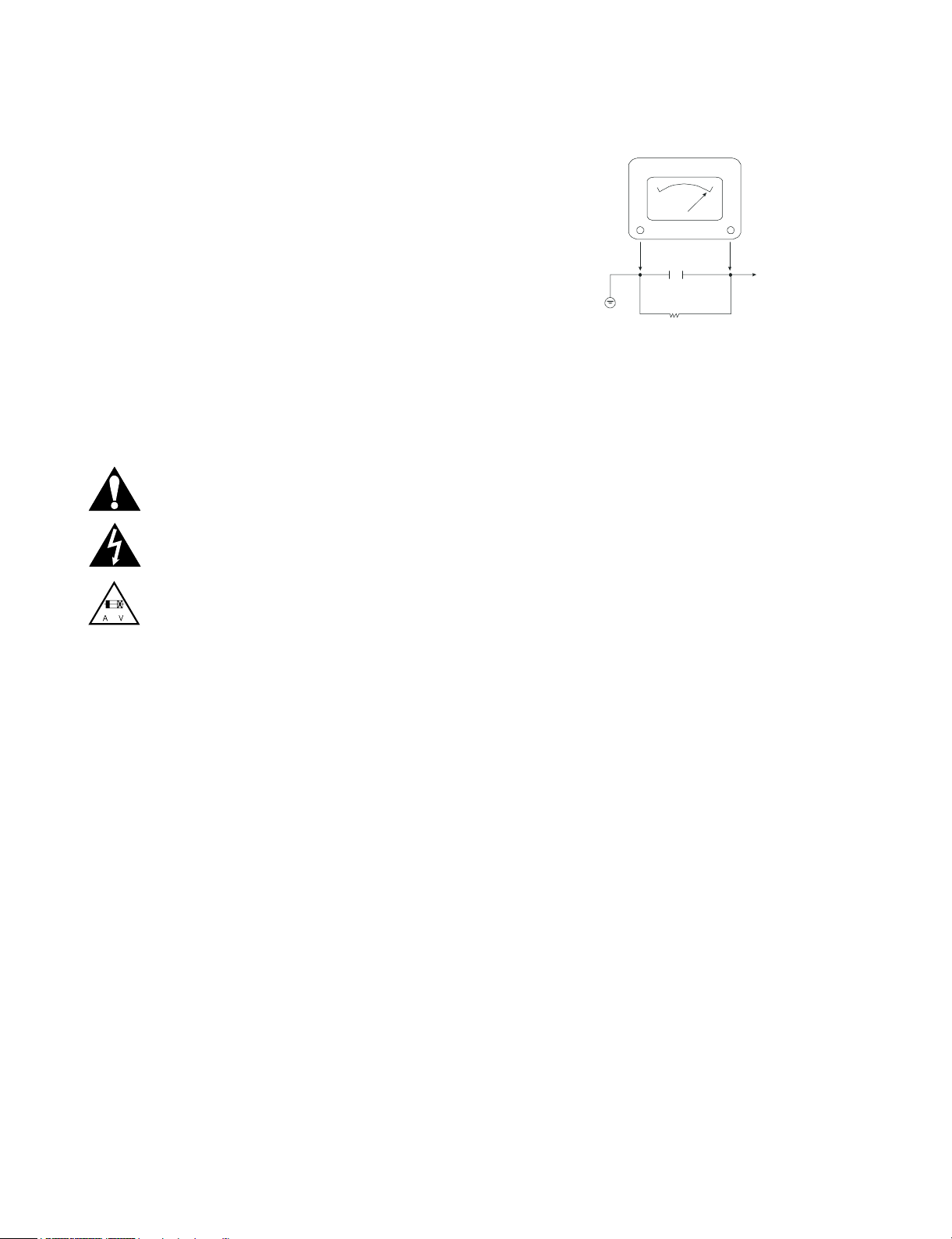
6. After reassembly of the set, always perform an AC leakage test on all
exposed metallic parts of the cabinet (the channel selector knobs, antenna
terminals, handle and screws) to be sure that set is safe to operate without
danger of electrical shock. DO NOT USE A LINE ISOLATION TRANSFORMER DURING THIS TEST. Use an AC voltmeter having 5000 ohms per
volt or more sensitivity in the following manner: Connect a 1500 ohm, 10
watt resistor, paralleled by a .15 mfd 150V AC type capacitor between a
known good earth ground water pipe, conduit, etc.) and the exposed metallic parts, one at a time. Measure the AC voltage across the combination of
1500 ohm resistor and .15 mfd capacitor. Reverse the AC plug by using a
non-polarized adaptor and repeat AC voltage measurements for each
exposed metallic part. Voltage measured must not exceed 0.75 volts RMS.
This corresponds to 0.5 milliamp AC. Any value exceeding this limit constitutes a potential shock hazard and must be corrected immediately.
TIPS ON PROPER INSTALLATION
1. Never install any receiver in a closed-in recess, cubbyhole, or closely fitting
shelf space over, or close to, a heat duct, or in the path of heated air flow.
2. Avoid conditions of high humidity such as: outdoor patio installations where
dew is a factor, near steam radiators where steam leakage is a factor, etc.
3. Avoid placement where draperies may obstruct venting. The customer
should also avoid the use of decorative scarves or other coverings that
might obstruct ventilation.
4. Wall- and shelf-mounted installations using a commercial mounting kit must
follow the factory-approved mounting instructions. A product mounted to a
shelf or platform must retain its original feet (or the equivalent thickness in
spacers) to provide adequate air flow across the bottom. Bolts or screws
used for fasteners must not touch any parts or wiring. Perform leakage tests
on customized installations.
5. Caution customers against mounting a product on a sloping shelf or in a tilted position, unless the receiver is properly secured.
6. A product on a roll-about cart should be stable in its mounting to the cart.
Caution the customer on the hazards of trying to roll a cart with small casters across thresholds or deep pile carpets.
7. Caution customers against using extension cords. Explain that a forest of
extensions, sprouting from a single outlet, can lead to disastrous consequences to home and family.
A.C. Voltmeter
1500 OHM
10 WATT
Place this probe
on each exposed
metal part.
Good Earth Ground
such as the Water
Pipe, Conduit, etc.
0.15uF
PRODUCT SAFETY SERVICING GUIDELINES FOR VIDEO PRODUCTS

1-4
SERVICING PRECAUTIONS
CAUTION : Before servicing the DVD Recorder covered by
this service data and its supplements and addends, read and
follow the
SAFETY PRECAUTIONS. NOTE : if unforeseen
circumstances create conflict between the following servicing precautions and any of the safety precautions in this publications, always follow the safety precautions.
Remembers Safety First:
General Servicing Precautions
1. Always unplug the DVD Recorder AC power cord from the
AC power source before:
(1) Removing or reinstalling any component, circuit board,
module, or any other assembly.
(2) Disconnection or reconnecting any internal electrical
plug or other electrical connection.
(3) Connecting a test substitute in parallel with an elec-
trolytic capacitor.
Caution : A wrong part substitution or incorrect
polarity installation of electrolytic capacitors may result
in an explosion hazard.
2. Do not spray chemicals on or near this DVD Recorder or
any of its assemblies.
3. Unless specified otherwise in this service data, clean
electrical contacts by applying an appropriate contact
cleaning solution to the contacts with a pipe cleaner,
cotton-tipped swab, or comparable soft applicator.
Unless specified otherwise in this service data, lubrication
of contacts is not required.
4. Do not defeat any plug/socket B+ voltage interlocks with
whitch instruments covered by this service manual might
be equipped.
5. Do not apply AC power to this DVD Recorder and/or any
of its electrical assemblies unless all solid-state device
heat sinks are cerrectly installed.
6. Always connect test instrument ground lead to the
appropriate ground before connection the test instrument
positive lead. Always remove the test instrument ground
lead last.
Insulation Checking Procedure
Disconnect the attachment plug from the AC outlet and turn
the power on. Connect an insulation resistance meter(500V)
to the blades of the attachment plug. The insulation resistance between each blade of the attachment plug and accessible conductive parts (Note 1) should be more than 1Mohm.
Note 1 : Accessible Conductive Parts including Metal panels, Input terminals, Earphone jacks, etc.
Electrostatically Sensitive (ES) Devices
Some semiconductor (solid state) devices can be damaged
easily by static electricity. Such components commonly are
called Electrostatically Sensitive (ES) Devices. Examples of
typical ES devices are integrated circuits and some field
effect transistors and semiconductor chip components.
The following techniques should be used to help reduce the
incidence of component damage caused by static electricity.
1. Immediately before handling any semiconductor component or semiconductor-equipped assembly, drain off any
electrostatic charge on your body by touching a known
earth ground. Alternatively, obtain and wear a commercially available discharging wrist strap device, which
should be removed for potential shock reasons prior to
applying power to the unit under test.
2. After removing an electrical assembly equipped with ES
devices, place the assembly on a conductive surface such
as aluminum foil, to prevent electrostatic charge buildup or
exposure of the assembly.
3. Use only a grouned-tip soldering iron to solder or unsolder
ES devices.
4. Use only an anti-static solder removal device. Some
solder removal devices not classified a “anti-static” can
generate electrical charges sufficient to damage ES
devices.
5. Do not use freon-propelled chemicals. These can
generate electrical charge sufficient to damage ES
devices.
6. Do not remove a replacement ES device from its protec
tive package until immediately before you are ready to
install it. (Most replacement ES devices are packaged with
leads electrically shorted together by conductive foam,
aluminum foil, or comparable conductive material).
7. Immediately before removing the protective material from
the leads of a replacement ES device, touch the protective
material to the chassis or circuit assembly into which the
device will be installed.
Caution : Be sure no power is applied to the chassis or
circuit, and observe all other safety precautions.
8. Minimize bodily motions when handling unpackaged
replacement ES devices. (Normally harmless motion such
as the brushing together of your clothes fabric or the lifting
of your foot from a carpeted floor can generate static electricity sufficient to damage an ES device.)
1-5
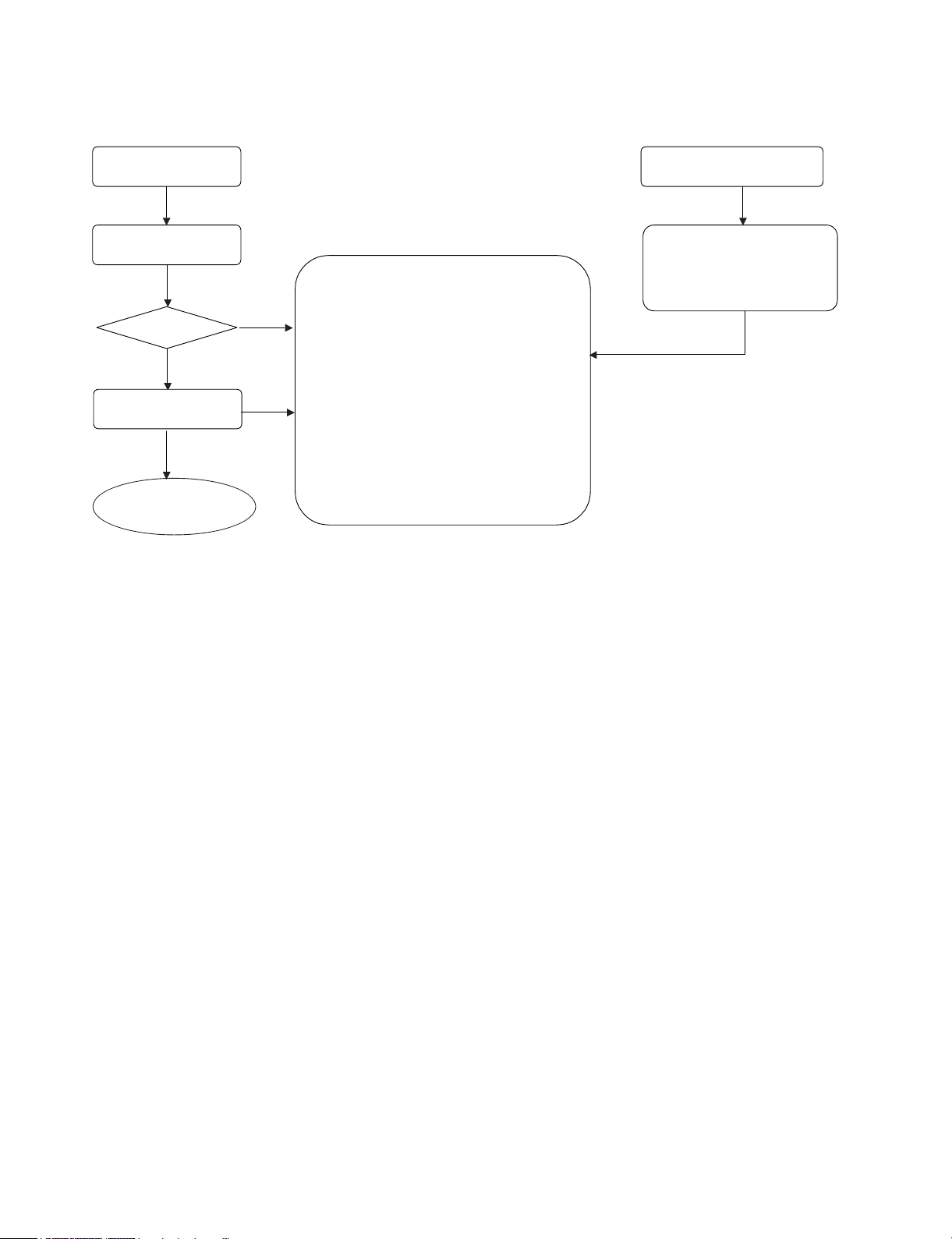
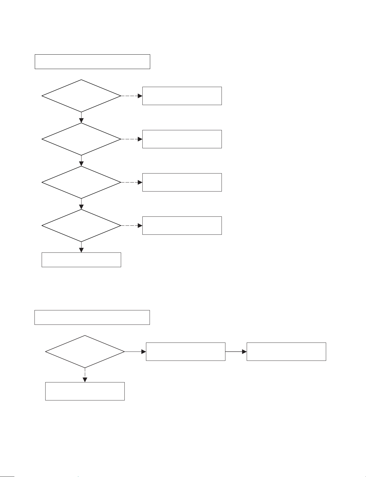
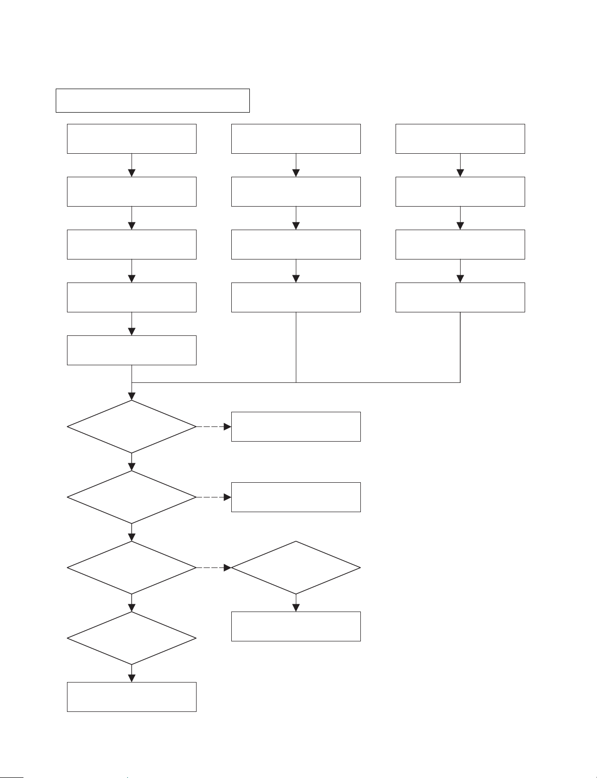
SERVICE INFORMATION FOR EEPROM IC SETTING
MICOM START
EEPROM ID CHECK
2 BYTE(B3,248,249)
ID OK?
OPTION DATA READ
5TIME & COMPARE
Yes
NAME HEX BINARY
OPT1 0C 00000000
00000000
00000000
00000000 (reserved)
00000000 (reserved)
00000000 (reserved)
OPT2 15
OPT3 00
OPT4 00
OPT5 08
OPT6 40
WRITE:OK EXIT:MENU, MP
MOVE:< > EDIT : __
OPTION WRITE : OK (OK KEY IN)
MASK : R00 , EEP : R00 , (D10)
(Each mask ,eeprom, It shows a development release
version.)
No
DETECT NEW EEPROM (OPTION EDIT SCREEN)
OPTION CONFIRMATION MODE
Press the "CLEAR" key on the
Remote controller and the "CH - " key
one the Front Panel the same
time, then it goes in to Tracking
initial mode.
OPTION condition of Present time
the CHECK There is a Possibility of
doing and the OPTION the REWRITE
it is possible.
*
MICOM NORMAL
OPERATION START
Yes
No
** EEPROM INITIAL ***
- SETUP is displayed in the field if pressing the Front ch- & ch+ Key with the Remocon number "clear"
key pressed in the status of powering on.
- AUTO SEARCH is done since the initial screen of ACMS is serviced if powering on.

1-6
SPECIFICATIONS
• GENERAL
Power requirements AC 200-240V, 50/60 Hz
Power consumption 44W
Dimensions (approx.) 430 X 92 X 382.5 mm (16.9 x 3.6 x 15 inches) (w x h x d)
Mass (approx.) 6.4 kg (14.1 lbs)
Operating temperature 5˚C to 35˚C (41˚F to 95˚F)
Operating humidity 5 % to 90 %
Television system PAL B/G colour system
Recording format PAL
• RECORDING
Recording format DVD VideoRecording, DVD-VIDEO
Recordable discs DVD-ReRecordable, DVD-Recordable
Recordable time Approx. 1 hour (HQ mode), 2 hours (SQ mode),
4 hours (LQ mode)
Video recording format
Sampling frequency 27MHz
Compression format MPEG 2
Audio recording format
Sampling frequency 48kHz
Compression format Dolby Digital
• DVD SPECIFICATIONS
Laser system Semiconductor laser
Frequency response DVD (PCM 48 kHz): 8 Hz to 22 kHz, CD: 8 Hz to 20 kHz
Signal-to-noise ratio More than 100 dB
Harmonic distortion Less than 0.008%
Dynamic range More than 95 dB
• INPUTS
AERIAL IN Aerial input, 75 ohms
VIDEO IN 1.0 Vp-p 75 ohms, sync negative, RCA jack x 2 / SCART
AUDIO IN 0 dBm more than 47 kohms, RCA jack (L, R) x 2 / SCART
DV IN 4 pin (i.LINK/IEEE 1394 standard)
• OUTPUTS
VIDEO OUT 1 Vp-p 75 Ω, sync negative, RCA jack x 1
S-VIDEO OUT (Y) 1.0 V (p-p), 75 Ω, negative sync, Mini DIN 4-pin x 1
(C) 0.3 V (p-p) 75 Ω
COMPONENT VIDEO OUT (Y) 1.0 V (p-p), 75 Ω, negative sync, RCA jack x 1
(Pb)/(Pr) 0.7 V (p-p), 75 Ω, RCA jack x 2
Audio output (digital audio) 0.5 V (p-p), 75 Ω, RCA jack x 1
Audio output (optical audio) 5 V (p-p), 75 Ω, Optical connector x 1
Audio output (analog audio) 2.0 Vrms (1 KHz, 0 dB), 600 Ω, RCA jack (L, R) x 1 / SCART
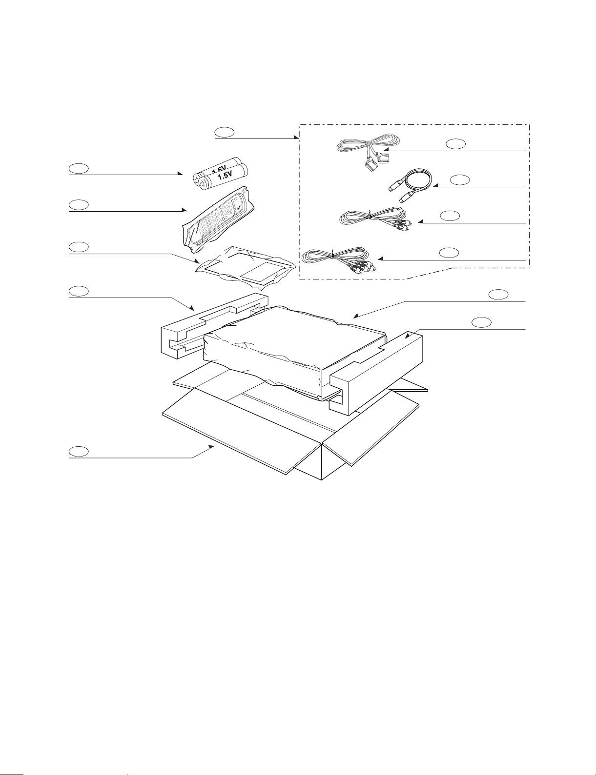
• ACCESSORY:
Video cable ..................................1 Audio cable . . . . . . . . . . . . . . .1
RF Coaxial Cable.........................1 Blank DVD-R disc . . . . . . . . . .2
Remote control ............................1 Batteries . . . . . . . . . . . . . . . . .2

2-1
SECTION 2
CABINET & MAIN CHASSIS
CONTENTS
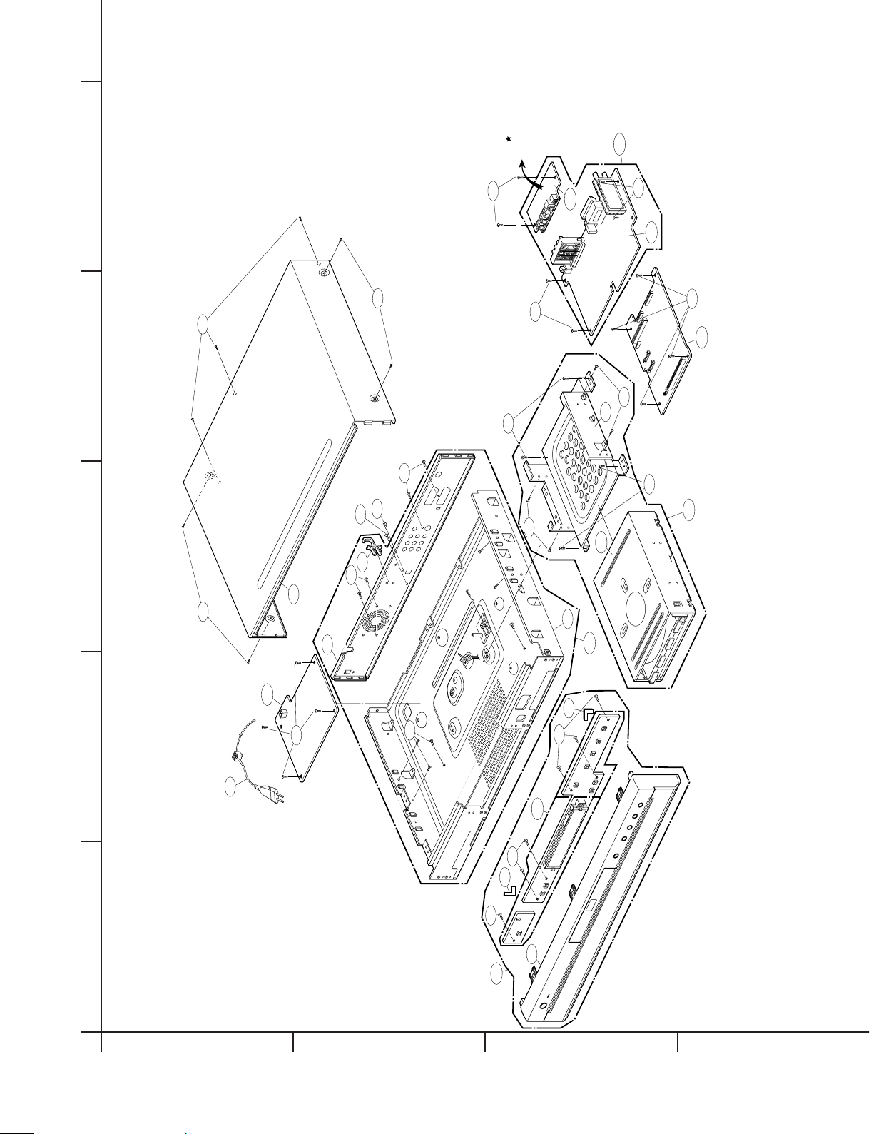
1. EXPLODED VIEWS ...............................................................................................................2-2
1. Cabinet and Main Frame Section ..........................................................................................2-2
2. Deck Mechanism Section(RL-01A) .......................................................................................2-3
3. Packing Accessory Section ...................................................................................................2-4
2-2
EXPLODED VIEWS
1. Cabinet and Main Frame Section
300
A47
463
463
463
250
A52
A46
A60
A43
A44
A50
280
452
286
452
452
286
260
320
465
466
463
466
270
465
467
463
463
463
463
467
467
265
463
463
A00
9TOOL ONLY
OUTSIDE
A52A
A52B
A
5
4
3
2
1
BCD
2-3
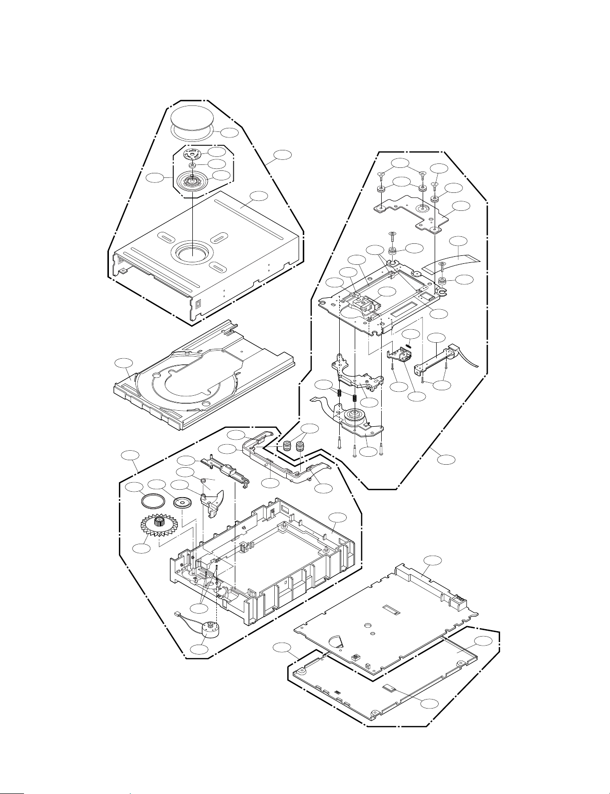
2. DECK MECHANISM SECTION(RL-01A)
001
004
005
431
431
036
030
025
028
035
034
038
029
033
023
022
031
433
032
025
432
021
037
037
026
011
019
019
019A
024
020
A01
A02
A51
A03
042
041
A01A
002
003
012
014
016
015
017
018
435
013
A04
027
2-4
808 Battery
Cable, Coaxial
Plug Ass'y, 1Way
Plug Ass'y, 2Way
Bag
Packing
Remote Control
Instruction Ass'y
Packing
Box
806
804
803
811
812
801
900
802
803
810
CABLE ASS'Y
821
SCART CABLE
3. Packing Accessory Section

3-1
SECTION 3
ELECTRICAL
CONTENTS
VDR PART
ELECTRICAL TROUBLESHOOTING GUIDE . . . . . . . .3-2
BLOCK DIAGRAMS . . . . . . . . . . . . . . . . . . . . . . . . . .3-16
1. LSI OVERALL BLOCK DIAGRAM . . . . . . . . . . . .3-16
2. IN/OUT BLOCK DIAGRAM . . . . . . . . . . . . . . . . .3-18
3. VIDEO IN/OUT BLOCK DIAGRAM . . . . . . . . . . .3-20
4. VIDEO SW PATH BLOCK DIAGRAM . . . . . . . . .3-22
5. AUDIO BLOCK DIAGRAM . . . . . . . . . . . . . . . . . 3-24
6. AUDIO SW PATH BLOCK DIAGRAM . . . . . . . . . 3-26
7. AUDIO IN/OUT BLOCK DIAGRAM . . . . . . . . . . .3-28
8. FLD/µ-COM/TUNER BLOCK DIAGRAM . . . . . . .3-30
9. POWER : MAIN BOARD BLOCK DIAGRAM . . . .3-32
10. POWER : I/O BOARD BLOCK DIAGRAM . . . . .3-34
11. POWER : LAYOUT CONNECTION BLOCK
DIAGRAM . . . . . . . . . . . . . . . . . . . . . . . . . . . .3-36
12. SMPS BLOCK DIAGRAM (PART 1) . . . . . . . . . .3-38
13. SMPS BLOCK DIAGRAM (PART 2) . . . . . . . . . .3-40
CIRCUIT DIAGRAMS . . . . . . . . . . . . . . . . . . . . . . . . .3-42
1. POWER CIRCUIT DIAGRAM . . . . . . . . . . . . . . .3-42
2. E5 BGA, POWER, UART2 CIRCUIT DIAGRAM .3-44
3. DDR SDRAM, FLASH CIRCUIT DIAGRAM . . . . .3-46
4. RST, CONTROL/STATUS REG, ATAPI, HOST
CPLD, LATCH CIRCUIT DIAGRAM . . . . . . . . . . .3-48
5. 1394, ETHERNET CONNECTOR
CIRCUIT DIAGRAM . . . . . . . . . . . . . . . . . . . . . .3-50
6. VIDEO IN/OUT CIRCUIT DIAGRAM . . . . . . . . . .3-52
7. AUDIO IN/OUT NON-STD VIDEO
CIRCUIT DIAGRAM . . . . . . . . . . . . . . . . . . . . . .3-54
8. I/O MICOM CIRCUIT DIAGRAM . . . . . . . . . . . . .3-56
9. I/O JACK CIRCUIT DIAGRAM . . . . . . . . . . . . . . .3-58
10. FRONT CIRCUIT DIAGRAM . . . . . . . . . . . . . . .3-60
11. FRONT JACK CIRCUIT DIAGRAM . . . . . . . . . .3-62
• WAVEFORMS . . . . . . . . . . . . . . . . . . . . . . . . . . . . .3-64
• CIRCUIT VOLTAGE CHART . . . . . . . . . . . . . . . . . .3-68
PRINTED CIRCUIT DIAGRAMS . . . . . . . . . . . . . . . . .3-72
1. MAIN P.C.BOARD(TOP SIDE) . . . . . . . . . . . . . .3-72
2. MAIN P.C.BOARD(BOTTOM SIDE) . . . . . . . . . . .3-74
3. I/O P.C.BOARD . . . . . . . . . . . . . . . . . . . . . . . . . .3-76
4. JACK P.C.BOARD . . . . . . . . . . . . . . . . . . . . . . . .3-76
5. FRONT P.C.BOARD . . . . . . . . . . . . . . . . . . . . . .3-78
6. LED P.C.BOARD (9TOOL ONLY) . . . . . . . . . . . .3-79
7. KEY P.C.BOARD . . . . . . . . . . . . . . . . . . . . . . . . .3-78
8. POWER P.C.BOARD . . . . . . . . . . . . . . . . . . . . . .3-79
RL-01A LOADER PART
ELECTRICAL TROUBLESHOOTING GUIDE . . . . . . .3-80
BLOCK DIAGRAMS & DESCRIPTION . . . . . . . . . . . .3-94
1. OVERALL BLOCK DIAGRAM . . . . . . . . . . . . . . .3-94
2. MAJOR IC INTERNAL BLOCK DIAGRAM AND
PIN DESCRIPTION . . . . . . . . . . . . . . . . . . . . . . .3-95
3. MAJOR IC INTERNAL BLOCK DIAGRAM AND
PIN DESCRIPTION . . . . . . . . . . . . . . . . . . . . . .3-100
4. IC302(UPD76F0047):MICOM . . . . . . . . . . . . . .3-109
WAVEFORMS . . . . . . . . . . . . . . . . . . . . . . . . . . . . . .3-113
1. POWER & RESET SIGNAL . . . . . . . . . . . . . . . .3-113
2. MAIN CLOCK1 FOR IC202 (16.9MHZ) . . . . . . .3-113
3. MAIN CLOCK2 FOR IC302 (20MHZ) . . . . . . . . .3-114
4. SDRAM CLOCK . . . . . . . . . . . . . . . . . . . . . . . .3-114
5. TRAY OPEN/CLOSE SIGNAL 1 . . . . . . . . . . . . .3-115
6. TRAY OPEN/CLOSE SIGNAL 2 . . . . . . . . . . . . .3-115
7. SLED MOVE SIGNAL 1 . . . . . . . . . . . . . . . . . . .3-116
8. SLED MOVE SIGNAL 2 . . . . . . . . . . . . . . . . . . .3-116
9. FOCUS SEARCH SIGNAL . . . . . . . . . . . . . . . .3-117
10. LASER TURN ON SIGNAL . . . . . . . . . . . . . . .3-117
11. DISC TYPE JUDGEMENT WAVEFORM
(CD SERIES) . . . . . . . . . . . . . . . . . . . . . . . . . .3-118
12. DISC TYPE JUDGEMENT WAVEFORM
(CD&CD-R) . . . . . . . . . . . . . . . . . . . . . . . . . . .3-118
13. DISC TYPE JUDGEMENT WAVEFORM
(CD-RW) . . . . . . . . . . . . . . . . . . . . . . . . . . . . .3-119
14. DISC TYPE JUDGEMENT WAVEFORM
(DVD SERIES) . . . . . . . . . . . . . . . . . . . . . . . .3-119
15. DISC TYPE JUDGEMENT WAVEFORM
(DVD_SINGLE&R) . . . . . . . . . . . . . . . . . . . . .3-120
16. DISC TYPE JUDGEMENT WAVEFORM
(DVD _DUAL) . . . . . . . . . . . . . . . . . . . . . . . . .3-120
17. DISC TYPE JUDGEMENT WAVEFORM
(DVDRW) . . . . . . . . . . . . . . . . . . . . . . . . . . . .3-121
18. SPINDLE WAVEFORM1 . . . . . . . . . . . . . . . . .3-121
19. SPINDLE WAVEFORM2 . . . . . . . . . . . . . . . . .3-122
20. FOCUS ON SIGNAL(CD) . . . . . . . . . . . . . . . .3-122
21. FOCUS ON SIGNAL(CD) . . . . . . . . . . . . . . . .3-123
22. FOCUS ON SIGNAL(DVD) . . . . . . . . . . . . . . .3-123
23. FOCUS ON SIGNAL (DVD) . . . . . . . . . . . . . . .3-124
24. TRACK OFF SIGNAL(CD) . . . . . . . . . . . . . . . .3-124
25. TRACK OFF SIGNAL(DVD) . . . . . . . . . . . . . . .3-125
26. TILT DRIVER SIGNAL(DISC READING) . . . . .3-125
27. RF WAVEFORM(DVD) . . . . . . . . . . . . . . . . . .3-126
28. RF WAVEFORM(CD) . . . . . . . . . . . . . . . . . . . .3-126
29. WOBBLE(DVD-R/RW)_READING . . . . . . . . . .3-127
30. WOBBLE(DVD+R/RW)_READING&WRITING
=>X1 SPEED . . . . . . . . . . . . . . . . . . . . . . . . .3-127
31. LD ENABLE(DVD) . . . . . . . . . . . . . . . . . . . . . .3-128
32. LD ENABLE(CD) . . . . . . . . . . . . . . . . . . . . . . .3-128
33. LASER POWER(READING)_DVD+RW . . . . . .3-129
34. LASER POWER(ERASE)_DVD+RW . . . . . . . .3-129
35. LASER POWER(WRITING)_INITIAL STATE . .3-130
36. LASER POWER(WRITING)_PROCESSING . .3-130
CIRCUIT DIAGRAMS . . . . . . . . . . . . . . . . . . . . . . . .3-131
1. RF CIRCUIT DIAGRAM . . . . . . . . . . . . . . . . . .3-131
2. DSP CIRCUIT DIAGRAM . . . . . . . . . . . . . . . . .3-133
3. µ-COM CIRCUIT DIAGRAM . . . . . . . . . . . . . . .3-135
PRINTED CIRCUIT DIAGRAMS . . . . . . . . . . . . . . . .3-137
1. MAIN P.C.BOARD(TOP SIDE) . . . . . . . . . . . . . .3-137
3-2
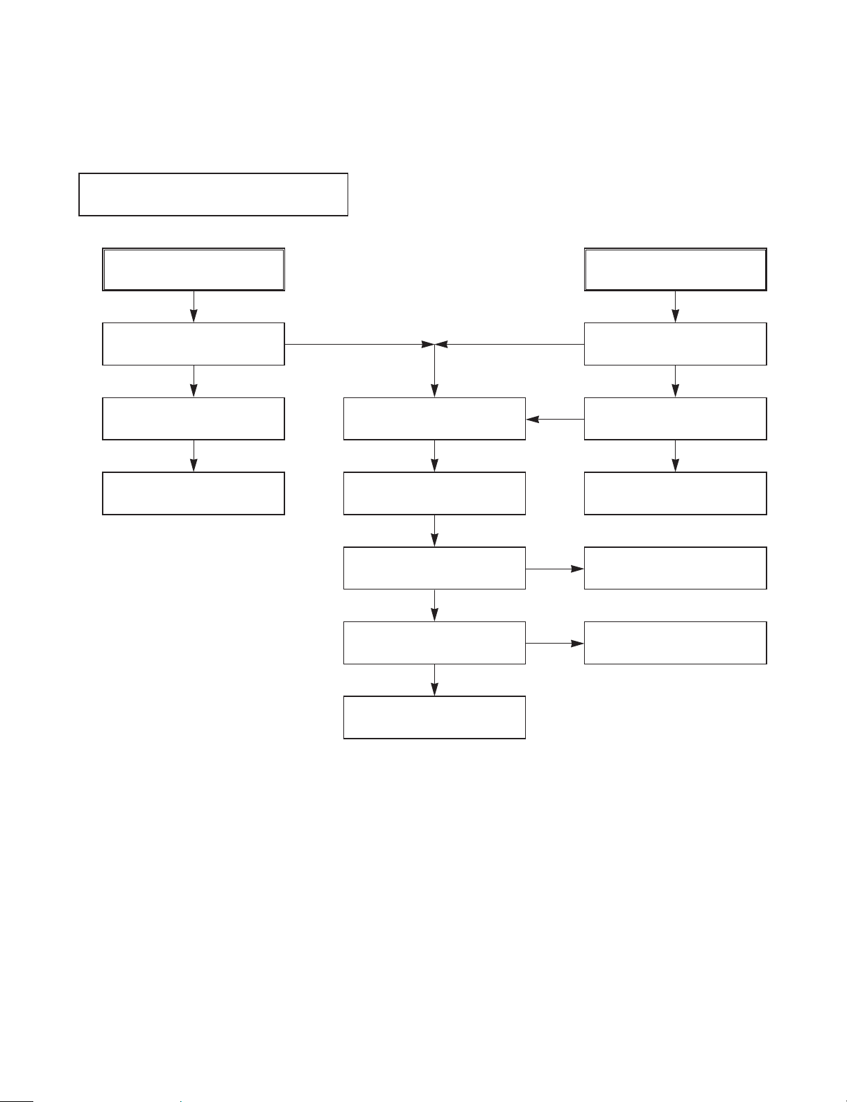
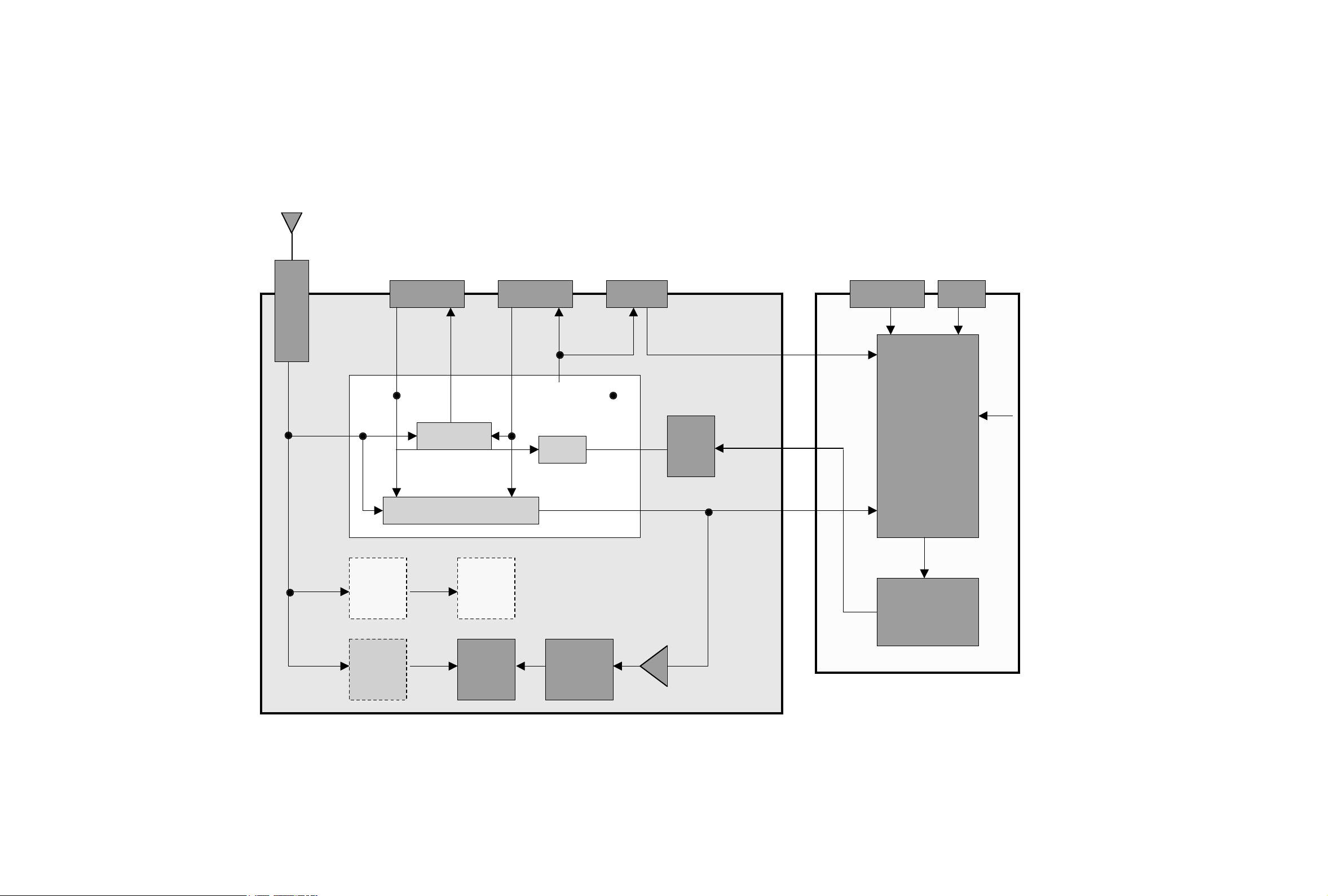
ELECTRICAL TROUBLESHOOTING GUIDE
VDR PART
No 5VD
No 5.2VA
Is 5.2VA section working?
Is 5.2V present at
emitter of Q120?
Replace Q120
Replace TH01
Replace BD101
No VF+
Is 5.2VA section working?
Replace R102
Check R102
NO
YES
YES
YES
Check F101
YES
Is there a DC voltage at
TH01?
YES
Is there a DC voltage
At (+) terminal of BD101?
Replace IC101
YES
YES
YES
YES
(Power ( SMPS ) Circuit (Part 1))
NO
NO
NO
NO
Power Section
3-3
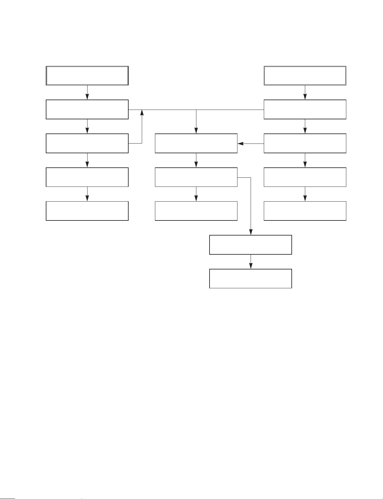
No 3.3V
No 3.8VA
Is 3.8VA section working?
Is there a DC voltage at
IC154 1PIN
Check IC154
Replace IC154
No 1.8V
Is 3.8VA section working?
Check IC160
Replace IC160
Is there a DC voltage at
IC160 1PIN
NO
NO
YES
YES
Is there a DC voltage
D122(-)?
YES
YES
Replace IC104
Check Polarity D122
Replace IC104
NO
YES
YES
YES
YES
(Power ( SMPS ) Circuit (Part 2))
NO
NO
3-4
IC2075 - 8 : HIGH?
( /E5_RST )
Check IC2075 power and other
circuits
X102 : Clock oscillated ?
( 13.5 MHz )
Replace X102
RESET
IC1057 - 26 : Check signal?
(E5_CS0 )
Check IC2085 signal flow
Check DRIVE power?
5V, 12V
Check SMPS
Check ATAPI Interface connector
H203
LG logo not displayed at
POWER ON
YES
NO
YES
NO
YES
NO
YES
NO
SYSTEM Section
DISC not recognized
Check IC1057 power and other
circuits
3-5
When playing DISC, no audio output
IC802 – 24,25,26,27
Check audio output
Check IC802 power and
other circuits
IC802 - 14 : HIGH ?
(AD/DAC RESET status)
Check IC2033 power and
other circuits
IC802 - 11,12 :
I2C signal normal?
Check R1A1, R118, R119, R121
Check IC802 power and
other circuits
IC702 - 46: HIGH ?
( LOW: AUDIO MUTE )
Check IC702 power and
other circuits
No OPTICAL / DIGITAL output
PN6701 - 2 signal normal?
Check TR701, JK704
power and other circuits
Check R120, FFC CABLE
signal flow
Check IC711 power and
other circuits
YES
NO
YES
NO
YES
YES
NO
NO NO
NO
3-6
No TUNER audio output
IC808,809 - 7
Check audio signal output
Check IC808,809 (AUDIO SWITCH) power and
Switching operation
Pin 2,4 High/Low =>Pin 7 output :
SW_A_OUT_L/R
IC7808,809-5
Check audio signal input
Audio output even when
playing DISC
< When playing DISC, no audio output. > Check
IC804 - 23,27
Check audio signal output
Check IC808,809 signal flow
and power
IC804 - 32,33
Check I2C signal flow
Q803 2(Emitter ) Hihg?
IC804 – 9:LOW?
HIGH: AUDIO MUTE
IC804 - 32,33
Check signal flow
IC702 - 46
LOW:AUDIO MUTE
IC804 – 20,24
Check audio signal input
Check R913,R914,C876,C877
signal flow
IC 807 - 30,31 :
No audio signal output
Check IC807 power and other
circuits Check X801 oscillated
YES
NO
YES
NO
YES
YES
YES
NO
NO
NO
YES
NO
YES
NO
NO
3-7
No TUNER VIDEO signal input
IC702 - 39 :
No Sync signal input
Check IC705 power and
other circuits
When
changing a channel, IC702 -
69 :HIGH after RESET signal?
Check TUNER power and
other circuits
Check IC702 power and
other circuits
IC807 - 2 : Check SIF
signal input\
Check C866, TUNER signal fl ow
Check Q702 ( V.Buffer TR) circuit
YES
NO
YES
NO
YES
YES
NO
3-8
No external input 1 audio
IC808,809 - 7
Check audio signal output
IC808,809 (AUDIO SWITCH)
Check power and switching operation
Pin 2,4 High/Low =>Pin 7 output :
SW_A_OUT_L/R
IC7808,809-5
Check audio signal input
Audio output
even when playing DISC
< When playing DISC, no audi o ou tput > Check
IC804 - 23,27
Check audio signal output
Check IC808,809 signal flow and
power
IC804 - 32,33
Check I2C signal flow
Q803 2(Emitter ) Hihg?
IC804 – 9:LOW?
HIGH: AUDIO MUTE
IC804 - 32,33
Check signal flow
IC702 - 46
LOW:AUDIO MUTE
IC804 - 10,16
Check audio signal input
JK803 – 2 ,6
Check input
END
YES
NO
YES
NO
YES
YES
YES
NO
YES
YES
NO
NO
NO
NO
3-9
No external input 2 audio
IC808,809 - 7
Check audio signal output
IC808,809 (AUDIO SWITCH)
Check power and switching operation
Pin 2,4 High/Low =>Pin 7 output :
SW_A_OUT_L/R
IC7808,809-5
Check audio signal input
Audio output
even when playing DISC
< No audio output when playing DISC > Check
IC804 - 23,27
Check audio signal output
Check IC808,809 signal flow
and power
IC804 - 32,33
Check I2C signal flow
Q803 2(Emitter ) Hihg?
IC804 – 9:LOW?
HIGH: AUDIO MUTE
IC804 - 32,33
Check signal flow
IC702 - 46
LOW:AUDIO MUTE
IC804 – 8,14
Check audio signal input
JK803 – 23,27
Check input
END
YES
NO
YES
NO
YES
NO
YES YES
YES
NO NO
NO
YES
NO
3-10
No external input 3 audio
END
IC808,809 - 7
Check audio signal output
IC808,809 (AUDIO SWITCH)
Check power and switching operation
Pin 2,4 High =>Pin 7 output : A1_L/R
Pin 2,4 High/Low =>Pin 7 output : TU_L/R
IC7808,809-5
Check audio signal input
Audio
output even when playing DISC
< No audio output when playing DISC > Check
Check JK801 Audio L/R terminal
YES
NO
YES
NO
YES
NO
3-11
No external input 4 audio
END
IC808,809 - 7
Check audio signal output
IC808,809 (AUDIO SWITCH)
Check power and switching operation
Pin 2,4 Low =>Pin 7 output : A2_L/R
Pin 2,4 High/Low =>Pin 7 output : TU_L/R
IC7808,809-1
Check audio signal input
Audio
output even when playing DISC
< No audio output when playing DISC > Check
Check PN802 FFC Cable 1,3
Check JK 762,763 terminal
END
YES
NO
YES
NO
YES
NO
YES
NO
3-12
No RGB /
Component video signal when playing DISC
SW801 Q High?
IC7042 - 49 : HIGH ?
Check other circuits around
IC702
Q808 Collector High?
signal after checking R951,952,
953,956 and FFC CABLE?
IC4003 - 8 : HIGH ?
/RST_VIDEO
IC4003-4
Check Clock signal input
IC4003- 9~16
Check VO_D0-~VO_D7 signal
IC1099 => IC4003
Check VO_D0 ~ VO_D7 signal
IC2075-8
Check signal
Check R112 CLOCK
Check IC4009-31,32 signal
and 5V power
Check IC4002
power and other circuits
Check IC702 ñ 85 :High input
IC806 ñ 16,18,20
R,G,B output?
IC806power and other circuits
IC806 – 16,18,21
Pr,Pb,Y output?
IC4003 –41,42
Check I2C CLK, DATA
YES
NO
YES YES
NO
YES YES
NO
YES
YES
YES
YES YES
YES
NO
NO
NO
NO
NO
3-13
No COMPOSIT / S-VIDEO signal when playing DISC
S-VIDEO: No Y signal?
Check R956,896
No COMPOSIT signal?
S-VIDEO : No C signal?
IC806 - 3
Check output
Check R954,C896
IC4003 - 8 : HIGH ?
/RST_VIDEO
Check IC4003-4
Clock signal input
IC4003 ñ41,42
Check I2C CLK, DATA
IC4003- 9~16
Check VO_D0-~VO_D7 signal
IC1099 => IC4003
Check VO_D0 ~ VO_D7 signal
IC2075-8
Check signal
Check R112 CLOCK
Check IC4009-31,32
signal and 5V power
Check IC4002 power and
other circuits
Check R810,C927
IC804 – 29,30
Check output
Check R804,C892
IC806 - 21
Check output
Check R918,C925
IC806 - 26
Check output
Check R821,C821
YES
YES
YES
YES
YES
YES
YES
YES
YES
YES
YES
YES
YES
YES
NO
YES
NO
YES
YES
YES
NO
3-14
No TV , external input video si gnal
No video signal of external input 1/ 2
( Rear Com osite i nput )
When connecting Tuner,
no TV video signal
No video signal of external input 3/4
( Front S-VIEDO / Comosite input )
Check IC804 - 28(input) and 31
(output), and thenCABLE =>
IC4009 signal input
IC4009 - 27 : HIGH ?
/RST_VIDEO
When RESET,
check IC4009 - 31,32
I2C CLK, DATA
Check IC4009 – 91,94 signal?
( VI_CLK, VI_VSYNC0 )
Check IC2075- 8,9 signal
Check IC4003- 40,41
signal and 5V LEVEL
Check X401 Clock oscillated
IC4009 => IC1099
Check VI_D0 ~ VI_D7 signal
Check IC4009 power and
other circuits
< When playing DISC, no COMPONENT, COMPOSIT/S-VIDEO signal > Check
Replace X401 X-TAL
Check Tuner power and other
circuits
JACK CABLE => IC4009
Check signal input
Check IC804 - 1,3(input) and 31
(output), and then CABLE =>
IC4009 signal input
YES
YES
YES
YES
YES
YES
YES
NO
YES
NO
YES
NO NO
YES
YES
NO
3-15
No DV( IEEE 1394 ) input (video/audio) signal
Check DV_JACK and CABLE
connection
IC3048 - 42,43,44,45
Check signal input
IC3048 - 78:HIGH?
( /RST_PHY )
Check IC2075 –8 signal
Check IC3048 - 2 Clock?
BIO_PHY_CLK
Check X301 Clock
24.576 MHz
IC3048 => IC1099
Check BIO_PHY_DATA/CLK
signal
Check IC3048 power and
other circuits
< When playing DISC, No COMPONENT, COMPOSIT/S-VIDEO signal > Check
YES
YES
YES
NO
YES
NO
YES
NO
3-16 3-17
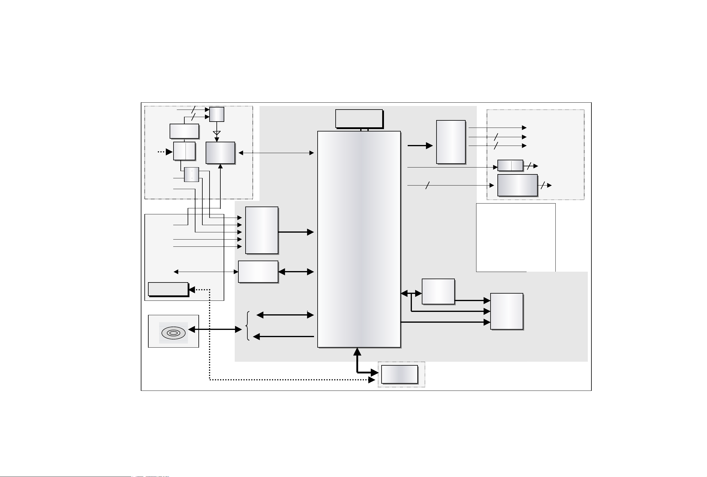
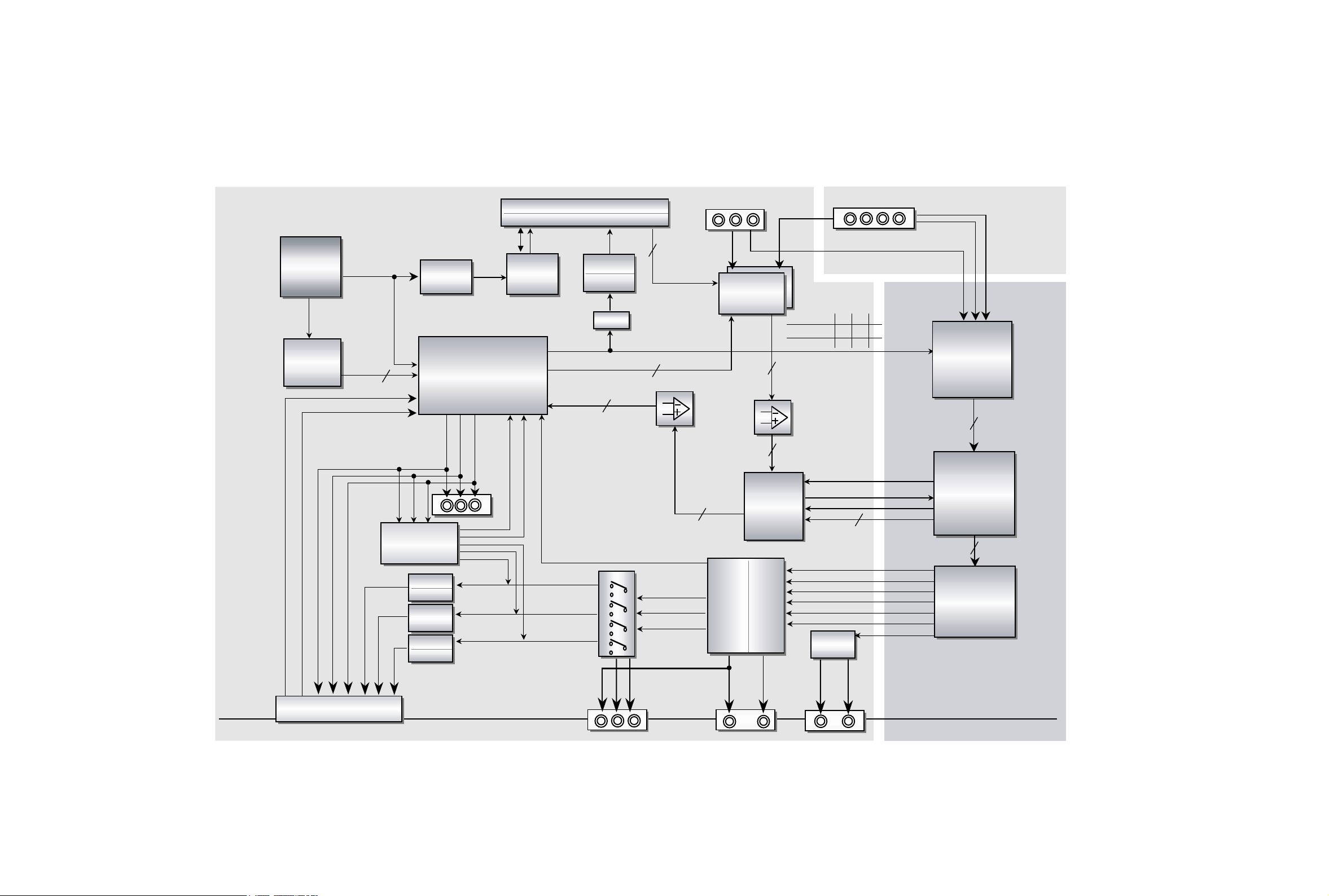
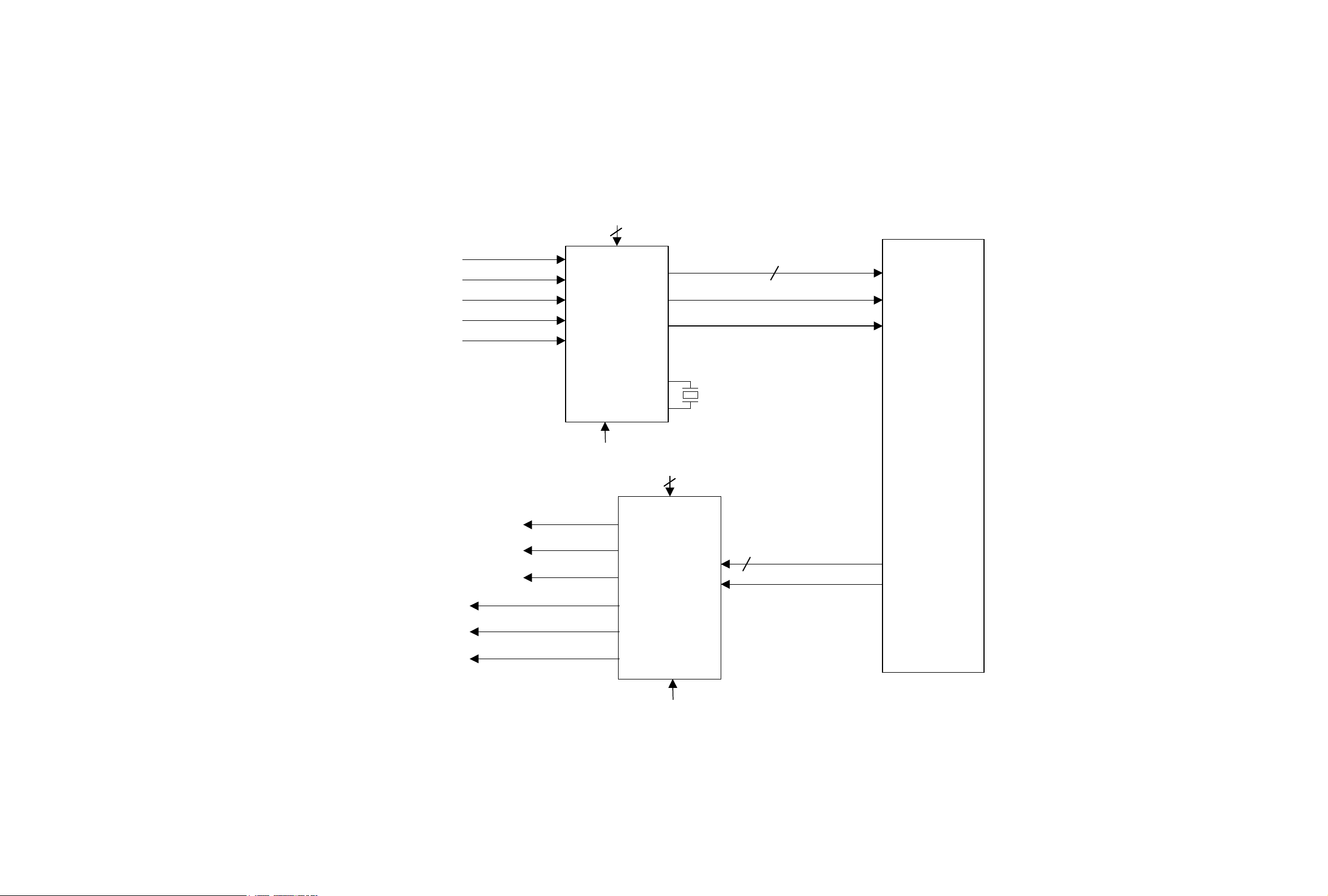
BLOCK DIAGRAMS
1. LSI Overall Block Diagram
Front U-com
V_DEC
Decoder
SAA7115
A_ADC
CS4271
RF
S1 / S2
A1_In
Tuner
S/PDIF
DMN8600
V_ENC
SAA7128
SW
A_ADC:2ch
CS4271
V2_In
S_In
A2_In
I/O Bíd
Front Jack Bíd
AI_D0
V1_IN
CVBS_Out
I/O Bíd
S_VIDEO_Out
Y/Pb/Pr or R/G/B
Analog
Audio Out
Optical & Digital
Audio Out
BIO_PHY_DATA[0:7]
PHY
TSB41LV03A
DV_In
HD[0:15]
UART1
UART2 / GPIO
JTAG
A0_D
0
A0_IEC958
V0_D[0:15]
ATAPI_DATA[0:15]
ATAPI_...
DVD-RW DRIVE
DDR SDRAM
8M WordX4
I/O Bíd
U-COM
HOST_RXD
HOST_TXD
(156.25KHz)
MAIN Bíd
Latch
74LVT16373
BA[6:21]
Flash
4MByte
SW
V1_In
N/A2
MSP3417
BA[1:5],BA22
3-18 3-19
2. In/Out Block Diagram
TUNER
CVBS
Y
G (Y)
B (Pb)
R (Pr)
G(Y) OUT
B(Pb) O UT
R(Pb) O UT
G_SCART_OUT
B_SCART_OUT
R_SCART_OUT
R SCART I N
B SCART IN
G SCART IN
SCART 1
MM1225
V_SWITCH
MM1225
V_SWITCH
MM1225
V_SWITCH
SDA5650
VPS
MM1510
6dB Buffer
SW_V_OUT
C
Y OUT
C OUT
CVBS OUT
CVBS OUT
MM1109
Sync
Seperator
Pb
Pr
Y
SW801
G_SCART_OUT
R_SCART_OUT
B_SCART_OUT
I2C
DAV
C_SYNC_IN
MSP3417
AUDIO
Processor
TU _A_L/R
NJM2521
AUDIO
SWICH
A1 L/R IN
AI_DO
AO_DO
DAC_MCLK
AO_FSYNC
AO_SCLK
A_OUT_L/R
Audio Out
L
Audio Out
R
AUDIO OUT L
CVBS OUT
AUDIO OUT R
74HCT04
INVERTER
AO_IEC958
OPTICA
L
COAXIAL
TU A OUT
HIGH :From S CART2
LO W:From SW801
HIGH:G/B/R
LOW:Y/Pb/Pr
SW_A_OUT` L/R
I/O U-COM
0dB
Buffer
EU2_A_IN_L/R
EU1_V_IN
EU1_A_IN_L/R
FRONT JACK
I/O JACK
A2 L/R IN
V2 IN
Y/C IN
TU_V_OUT
Audio_Sel_1
Audio_Sel_2
Audio_Out
H
H
HLLL
A1 SW A2
AUDIO SEL 1,2
CS4271
AUDIO
CODEC
DMM8600
MPEG
ENC/DEC
SCART 2
EU2_V_IN
MM1443
AV SWITCH
Built in 6dB
SAA7115
Video
Decoder
(ADC)
MM1623
VIDEO
Buffer
FRONT JACK
MAIN BOARD
I/O BOARD
V1 IN
I2C
SAA7128
Video
Encoder
(DAC)
VI-D0/D7
V0_D0/D7
3-20 3-21
3. Video In/Out Block Diagram
IC4009
SAA7115
VIDEO
Decoder
VI_D[0:7]
TU_Vz_IN
Y_IN
C_IN
V1_IN
V2_IN
VI_CLK
VI_VSYNCO
IC4003
SAA7128
VIDEO
Encoder
VO_D[0:7]
Y
C
CVBS
SCL/SDA
SCL/SDA
24.576MHz
VO_CLK
IC1099
DMN8600
/RST_VIDEO
/RST_VIDEO
R / Pr
G / Y
B / Pb
3-22 3-23
4. Video SW Path Block Diagram
TU
S2 S1 AV3
IC805
MM1510
(6dB,75 )
IC811
SDA5650
(VPS)
IC706
MM1510
(6dB,75 )
IC702
(u-COM)
IC705
MM1109
(Sync SEP.)
IC806
MM1623
(6dB A.)
B
AV4/S-V
V.DEC
V.ENC
TU_V_OUT
SW_V_OUT(TU/E1/E2)
CVBS_OUT
V1_IN
PB_IN
SW1
SW3
SW2
28
3
30
1
29
5
31
DV
 Loading...