

Page 1

MODELS : DP481B/DP482BSERVICE MANUAL
Internal Use Only
Website http://biz.lgservice.com
PORTABLE DVD
SERVICE MANUAL
MODELS : DP481B/DP482B
P/NO : AFN73065035
CAUTION
BEFORE SERVICING THE UNIT, READ THE “SAFETY PRECAUTIONS”
IN THIS MANUAL.
APRIL, 2009
Page 2
CONTENTS
SECTION 1.........SUMMARY
SECTION 2.........EXPLODED VIEWS
SECTION 3.........ELECTRICAL
SECTION 4.........REPLACEMENT PARTS LIST
1-1
Page 3

SECTION 1
SUMMARY
CONTENTS
PRODUCT SAFETY SERVICING GUIDELINES FOR VIDEO PRODUCTS .............................................. 1-3
SERVICING PRECAUTIONS .......................................................................................................................... 1-4
• GENERAL SERVICING PRECAUTIONS
• INSULATION CHECKING PRODEDURE
• ELECTROSTATICALLY SENSITIVE (ES) DEVICES
FIRMWARE UPGRADE METHOD ................................................................................................................. 1-5
SPECIFICATIONS ............................................................................................................................................ 1-7
1-2
Page 4
PRODUCT SAFETY SERVICING GUIDELINES FOR VIDEO PRODUCTS
IMPORTANT SAFETY NOTICE
This manual was prepared for use only by properly trained audio-video service
technicians.
When servicing this product, under no circumstances should the original design be
modified or altered without permission from LG Corporation. All components should
be replaced only with types identical to those in the original circuit and their physical
location, wiring and lead dress must conform to original layout upon completion of
repairs.
Special components are also used to prevent x-radiation, shock and fire hazard.
These components are indicated by the letter “x” included in their component designators and are required to maintain safe performance. No deviations are allowed
without prior approval by LG Corporation.
Circuit diagrams may occasionally differ from the actual circuit used. This way,
implementation of the latest safety and performance improvement changes into the
set are not delayed until the new service literature is printed.
CAUTION: Do not attempt to modify this product in any way. Never perform cus-
tomized installations without manufacturer’s approval. Unauthorized modifications
will not only void the warranty, but may lead to property damage or user injury.
Service work should be performed only after you are thoroughly familiar with these
safety checks and servicing guidelines.
GRAPHIC SYMBOLS
The exclamation point within an equilateral triangle is intended to
alert the service personnel to important safety information in the
service literature.
The lightning flash with arrowhead symbol within an equilateral
triangle is intended to alert the service personnel to the presence of
noninsulated “dangerous voltage” that may be of sufficient magnitude
to constitute a risk of electric shock.
The pictorial representation of a fuse and its rating within an equilateral triangle is intended to convey to the service personnel the
following fuse replacement caution notice:
CAUTION: FOR CONTINUED PROTECTION AGAINST RISK
OF FIRE, REPLACE ALL FUSES WITH THE SAME TYPE AND
RATING AS MARKED NEAR EACH FUSE.
SERVICE INFORMATION
While servicing, use an isolation transformer for protection from AC line shock. After
the original service problem has been corrected, make a check of the following:
FIRE AND SHOCK HAZARD
1. Be sure that all components are positioned to avoid a possibility of adjacent
component shorts. This is especially important on items trans-ported to and from
the repair shop.
2. Verify that all protective devices such as insulators, barriers, covers, shields,
strain reliefs, power supply cords, and other hardware have been reinstalled per
the original design. Be sure that the safety purpose of the polarized line plug has
not been defeated.
3. Soldering must be inspected to discover possible cold solder joints, solder
splashes, or sharp solder points. Be certain to remove all loose foreign particles.
4. Check for physical evidence of damage or deterioration to parts and components, for frayed leads or damaged insulation (including the AC cord), and
replace if necessary.
5. No lead or component should touch a high current device or a resistor rated at 1
watt or more. Lead tension around protruding metal surfaces must be avoided.
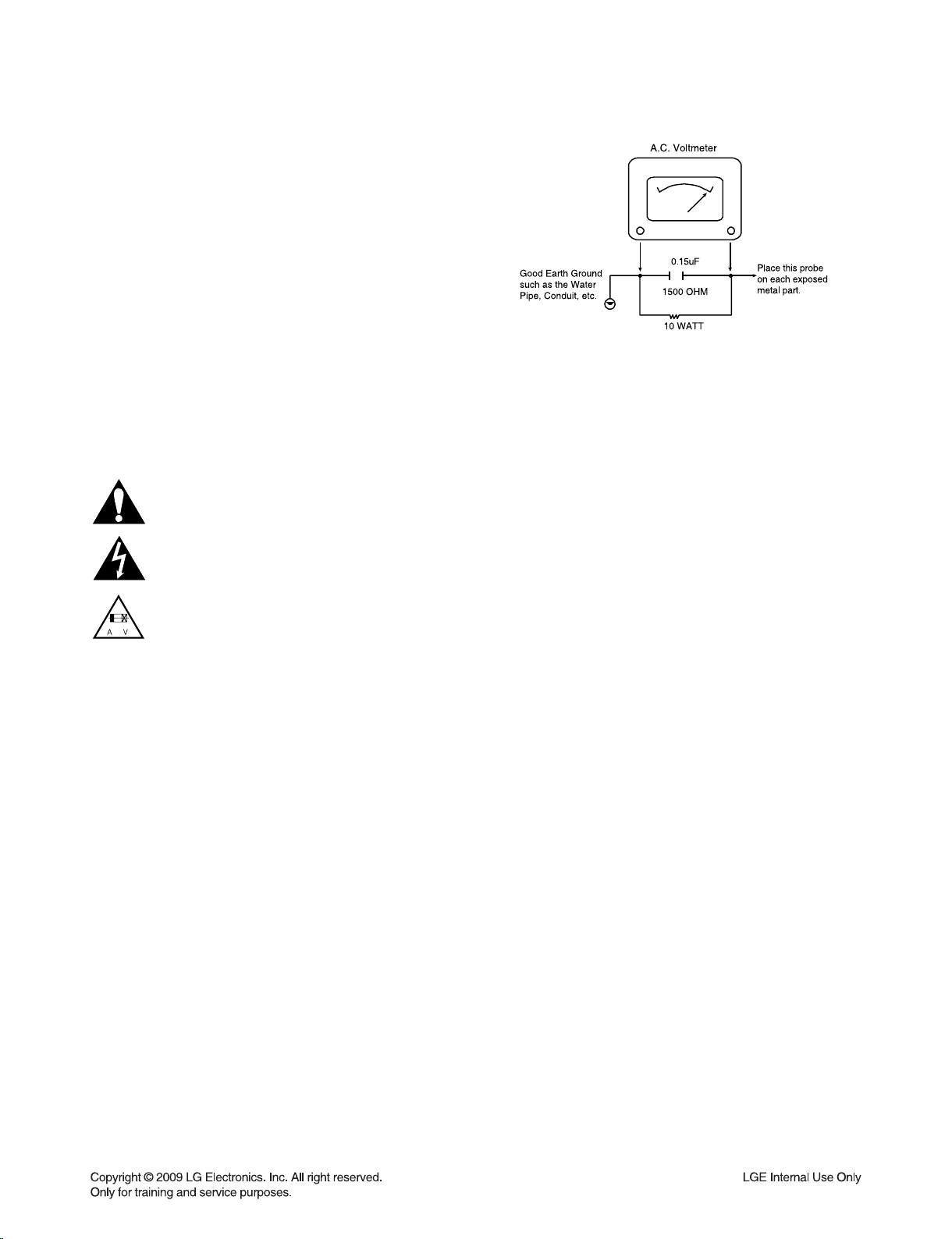
6. After reassembly of the set, always perform an AC leakage test on all exposed
metallic parts of the cabinet (the channel selector knobs, antenna terminals,
handle and screws) to be sure that set is safe to operate without danger of
electrical shock. DO NOT USE A LINE ISOLATION TRANSFORMER DURING
THIS TEST. Use an AC voltmeter having 5000 ohms per volt or more sensitivity
in the following manner: Connect a 1500 ohm, 10 watt resistor, paralleled by a
.15 mfd 150V AC type capacitor between a known good earth ground water pipe,
conduit, etc.) and the exposed metallic parts, one at a time. Measure the AC voltage across the combination of 1500 ohm resistor and .15 mfd capacitor. Reverse
the AC plug by using a non-polarized adaptor and repeat AC voltage measurements for each exposed metallic part. Voltage measured must not exceed 0.75
volts RMS. This corresponds to 0.5 milliamp AC. Any value exceeding this limit
constitutes a potential shock hazard and must be corrected immediately.
TIPS ON PROPER INSTALLATION
1. Never install any receiver in a closed-in recess, cubbyhole, or closely fitting shelf
space over, or close to, a heat duct, or in the path of heated air flow.
2. Avoid conditions of high humidity such as: outdoor patio installations where dew
is a factor, near steam radiators where steam leakage is a factor, etc.
3. Avoid placement where draperies may obstruct venting. The customer should
also avoid the use of decorative scarves or other coverings that might obstruct
ventilation.
4. Wall- and shelf-mounted installations using a commercial mounting kit must
follow the factory-approved mounting instructions. A product mounted to a shelf
or platform must retain its original feet (or the equivalent thickness in spacers) to
provide adequate air flow across the bottom. Bolts or screws used for fasteners
must not touch any parts or wiring. Perform leakage tests on customized installations.
5. Caution customers against mounting a product on a sloping shelf or in a tilted
position, unless the receiver is properly secured.
6. A product on a roll-about cart should be stable in its mounting to the cart.
Caution the customer on the hazards of trying to roll a cart with small casters
across thresholds or deep pile carpets.
7. Caution customers against using extension cords. Explain that a forest of extensions, sprouting from a single outlet, can lead to disastrous consequences to
home and family.
1-3
Page 5

SERVICING PRECAUTIONS
CAUTION: Before servicing the PORTABLE DVD covered by
this service data and its supplements and addends, read and
follow the SAFETY PRECAUTIONS. NOTE: if unforeseen
circumstances create conflict between the following servicing
precautions and any of the safety precautions in this publication, always follow the safety precautions.
Remember Safety First :
General Servicing Precautions
1. Always unplug the PORTABLE DVD AC power cord from
the AC power source before:
(1) Removing or reinstalling any component, circuit board,
module, or any other assembly.
(2) Disconnecting or reconnecting any internal electrical
plug or other electrical connection.
(3) Connecting a test substitute in parallel with an electro-
lytic capacitor.
Caution: A wrong part substitution or incorrect polarity
installation of electrolytic capacitors may result in an
explosion hazard.
2. Do not spray chemicals on or near this PORTABLE DVD or
any of its assemblies.
3. Unless specified otherwise in this service data, clean electrical contacts by applying an appropriate contact cleaning
solution to the contacts with a pipe cleaner, cotton-tipped
swab, or comparable soft applicator.
Unless specified otherwise in this service data, lubrication
of contacts is not required.
4. Do not defeat any plug/socket B+ voltage interlocks with
which instruments covered by this service manual might be
equipped.
5. Do not apply AC power to this PORTABLE DVD and / or
any of its electrical assemblies unless all solid state device
heat sinks are correctly installed.
6. Always connect the test instrument ground lead to an
appropriate ground before connecting the test instrument
positive lead. Always remove the test instrument ground
lead last.
Insulation Checking Procedure
Disconnect the attachment plug from the AC outlet and
turn the power on. Connect an insulation resistance meter
(500V)
to the blades of the attachment plug. The insulation resistance
between each blade of the attachment plug and accessible
conductive parts (Note 1) should be more than 1Mohm.
Note 1: Accessible Conductive Parts include Metal panels,
Input terminals, Earphone jacks,etc.
Electrostatically Sensitive (ES) Devices
Some semiconductor (solid state) devices can be damaged
easily by static electricity. Such components commonly are
called Electrostatically Sensitive (ES) Devices. Examples
of typical ES devices are integrated circuits and some field
effect transistors and semiconductor chip components.
The following techniques should be used to help reduce the
incidence of component damage caused by static electricity.
1. Immediately before handling any semiconductor component or semiconductor-equipped assembly, drain off any
electrostatic charge on your body by touching a known
earth ground. Alternatively, obtain and wear a commercially available discharging wrist strap device, which should
be removed for potential shock reasons prior to applying
power to the unit under test.
2. After removing an electrical assembly equipped with ES
devices, place the assembly on a conductive surface such
as aluminum foil, to prevent electrostatic charge buildup or
exposure of the assembly.
3. Use only a grounded-tip soldering iron to solder or unsolder
ES devices.
4. Use only an anti-static solder removal device. Some solder
removal devices not classified as “anti-static” can generate
electrical charges sufficient to damage ES devices.
5. Do not use freon-propelled chemicals. These can generate
an electrical charge sufficient to damage ES devices.
6. Do not remove a replacement ES device from its protective
package until immediately before you are ready to install
it. (Most replacement ES devices are packaged with leads
electrically shorted together by conductive foam, aluminum
foil, or comparable conductive material).
7. Immediately before removing the protective material from
the leads of a replacement ES device, touch the protective
material to the chassis or circuit assembly into which the
device will be installed.
Caution: Be sure no power is applied to the chassis or
circuit, and observe all other safety precautions.
8. Minimize bodily motions when handling unpackaged
replacement ES devices. (Normally harmless motion such
as the brushing together of your clothes fabric or the lifting
of your foot from a carpeted floor can generate static electricity sufficient to damage an ES device.)
1-4
Page 6
FIRMWARE UPGRADE METHOD
Please follow below process to download a program with disc
Advanced Preparation: USB, update file (target.bin) and platform.
Process:
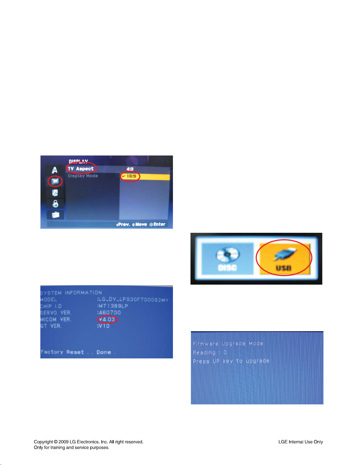
1. Turn on the Portable DVD player.
(Note: Be sure that there is no disc in PDVD)
2. Press “SETUP” button on remote control.
3. Choose a “display” menu by using the cursor button and then choose a “TV Aspect” menu.
And choose “16:9” menu.
< FIGURE 1. Progress to check system information >
4. Press the 1 → 3 → 9 → 7 → 1 → 3 → 9(numberial
button) → Enter key on remote control to confirm
the system information.
6. Change the program file name of new version to
the model name
Ex> New ver. Program file →
LG_DV_LP930F700082MY.ROM
Model name → LG_DV_LP930F700082MY
Change New ver. program file like this →
LG_DV_LP930F700082MY.ROM
If you don’t change the file name like that, Disc
download isn’t be worked.
7. Copy the changed file to a USB memory stick.
Note: the file must be at the root directory of USB.
8. Insert the copied USB memory stick to PDVD.
9. Press the MODE button on the PDVD-player.
10. Select USB mode.
5. Remember or write the model name.
< FIGURE 2. System information before update >
< FIGURE 3. Select the USB mode >
11. If the below picture appears on the screen, Select
“Start” and Press “UP” button on Remote controller. While this menu appears, please don’t eject
disc or take out USB
< FIGURE 4. System update mode interface >
1-5
Page 7
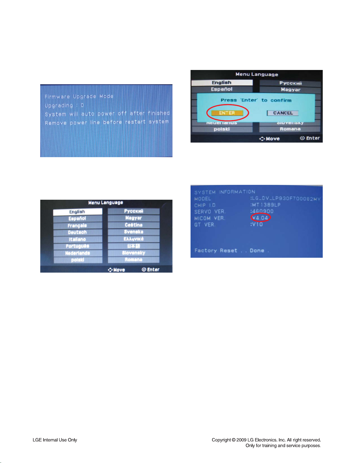
12. After the below picture appears on the screen, New
PDVD program will download from USB memory
stick automatically.
Do not take out USB memory stick.
< FIGURE 5. System updating >
13. After USB download is completed, PDVD-player
displays below picture automatically.
15. Select the initial Language and press “Enter” button. Then, Select “Enter” and press “Enter” button.
< FIGURE 7. Select initial language >
16. Do it again the progress 1, 2, 3, 4 to confirm the
version.
< FIGURE 6. System returns to MENU LANGUAGE
select interface >
14. Remove the USB memory stick.
FIGURE 8. Check the system information after updated >
1-6
Page 8

SPECIFICATIONS
• GENERAL
Power requirements DC 9V
Power consumption 12W
External Dimensions 221 x 32.7* x 175mm (W x H x D)
(*based upon the front side)
Net Weight (Approx.) 1.08kg
Operating temperature 0°C to 40°C
Operating humidity 5% to 90%
Laser Semiconductor laser
Signal system NTSC / PAL
• CONNECTORS
Audio/Video Output ø3.5mm mini jack x 1
- Video: 1.0V (p-p), 75Ω, sync negative
- Audio: 2.0Vrms (1kHz, 0dB)
Earphone terminal ø3.5mm stereo mini jack x 2
USB IN 4 pin (USB 2.0 / 1.1 standard)
• LIQUID CRYSTAL DISPLAY
Panel size 8.5 inches wide (diagonal)
Projection system R.G.B. stripe
Driving system TFT active matrix
Resolution 480 x 234 (WQVGA)
1-7
Page 9

MEMO
1-8
Page 10

SECTION 2
EXPLODED VIEWS
CONTENTS
EXPLODED VIEWS ......................................................................................................................................... 2-2
1. CABINET AND MAIN FRAME SECTION ................................................................................................. 2-2
2. PACKING ACCESSORY SECTION ......................................................................................................... 2-3
2-1
Page 11
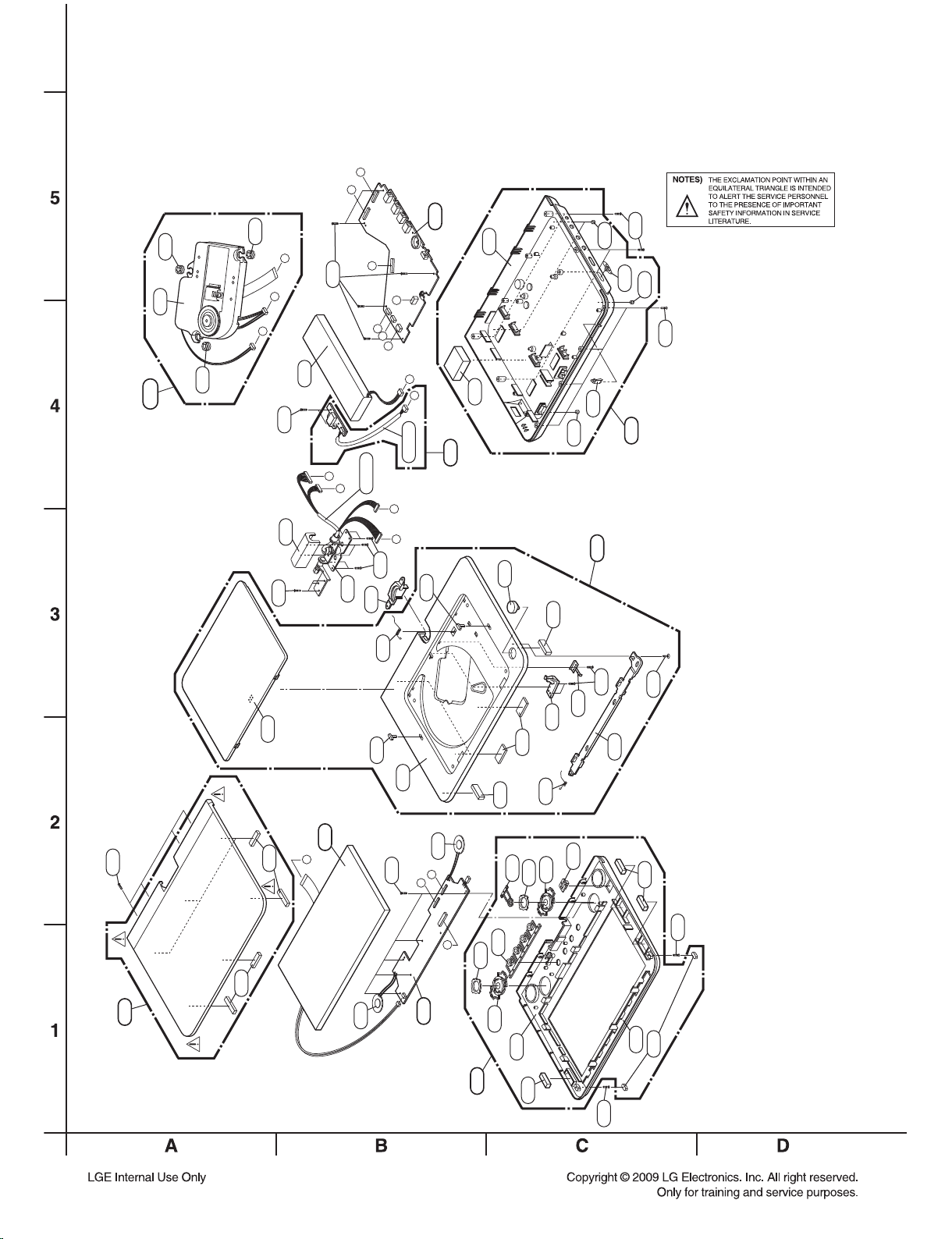
EXPLODED VIEWS
1. CABINET AND MAIN FRAME SECTION
E
D
A00
265
266
266
266
F
C
B
A46
G
F
CABLE2
276
260
263
264
A42
269
272
MAIN
BOARD
J
I
H
809
475
USB
279
486
476
BOARD
E
D
278
J
I
H
G
CABLE1
486
282
271
262
A43
264
261
474
264
474
A44
475
A48
281
268
281
477
277
275
259
A52
254
272
253
252
250
270
259
257
274
258
251
475
276
267
A40
A
LCD
280
475
B
C
A51
280
A
LCD/KEY
BOARD
273
255
485
257
475
256
2-2
Page 12
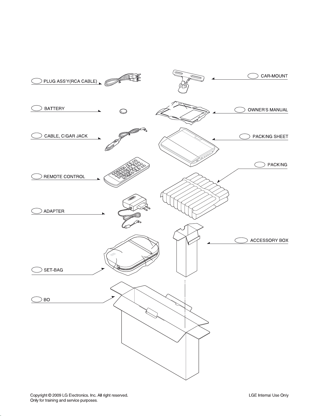
2. PACKING ACCESSORY SECTION
806
808
834
900
833
835
801
804
803
839
802
802A
X
2-3
Page 13

MEMO
2-4
Page 14

SECTION 3
ELECTRICAL
CONTENTS
LCD PART .......................................................3-2
LCD ELECTRICAL
TROUBLESHOOTING GUIDE
1. POWER CIRCUIT ........................................3-2
2. BJT AMPLIFIER FOR RGB
VIDEO CIRCUIT ...........................................3-2
3. IR REMOTE CONTROL CIRCUIT ...............3-2
...................3-2
BLOCK DIAGRAM ........................................3-3
CIRCUIT DIAGRAMS ...................................3-5
1. LCD TFT DRIVE CIRCUIT DIAGRAM .........3-5
2. KEYPAD CIRCUIT DIAGRAM .....................3-7
CIRCUIT VOLTAGE CHART ......................3-9
PRINTED CIRCUIT BOARD
DIAGRAMS
....................................................3-11
MAIN PART ...................................................3-15
MAIN ELECTRICAL
TROUBLESHOOTING GUIDE
1. POWER (DC-DC CONVERTER)
CIRCUIT .....................................................3-15
2. MPEG CIRCUIT .........................................3-18
3. SERVO CIRCUIT .......................................3-19
4. CHARGEING CIRCUIT ..............................3-21
.................3-15
WIRING DIAGRAM ......................................3-28
BLOCK DIAGRAMS ...................................3-29
1. OVERALL BLOCK DIAGRAM-1 .................3-29
2. OVERALL BLOCK DIAGRAM-2 .................3-30
3. POWER BLOCK DIAGRAM .......................3-31
4. SERVO BLOCK DIAGRAM ........................3-32
5. SYSTEM BLOCK DIAGRAM ......................3-33
6. AV BLOCK DIAGRAM ................................3-34
CIRCUIT DIAGRAMS .................................3-35
1. CHARGE GT6312 CIRCUIT DIAGRAM .....3-35
2. MPEG CIRCUIT DIAGRAM ......................3-37
3. DC-DC & MOTOR & OPU
CIRCUIT DIAGRAM ...................................3-39
4. SDRAM & FLASH CIRCUIT DIAGRAM .....3-41
5. AUDIO & VIDEO OUTPUT
CIRCUIT DIAGRAM ...................................3-43
6. PANEL CIRCUIT DIAGRAM ......................3-45
CIRCUIT VOLTAGE CHART ....................3-47
PRINTED CIRCUIT BOARD
DIAGRAMS
1. MAIN P.C. BOARD .....................................3-51
2. USB P.C. BOARD ......................................3-53
....................................................3-51
DETAILS AND WAVEFORMS ON
SYSTEM TEST AND DEBUGGING
1. SYSTEM 27MHz CLOCK, RESET
SIGNAL. .....................................................3-22
2. SDRAM CLOCK .........................................3-23
3. TRAY OPEN/CLOSE SIGNAL ...................3-24
4. SLED CONTROL RELATED SIGNAL ........3-24
5. LASER POWER CONTROL
RELATED SIGNAL .....................................3-25
6. SPINDLE CONTROL WAVEFORM ...........3-25
7. FOCUS ON WAVEFORM ..........................3-26
8. TRACKING CONTROL
RELATED SIGNAL(System checking) .......3-26
9. 1389LP VIDEO OUTPUT WAVEFORM .....3-27
10. 1389LP AUDIO OUTPUT WAVEFORM .....3-27
.......3-22
3-1
Page 15
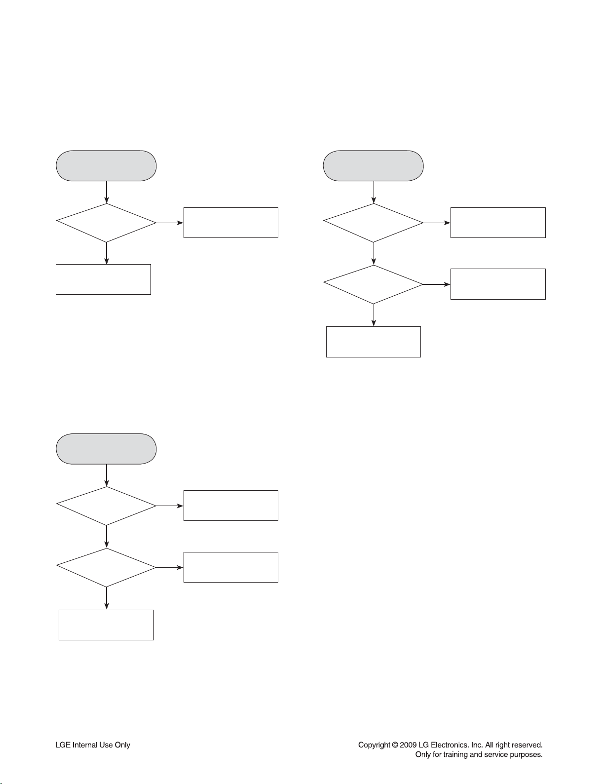
LCD PART
LCD ELECTRICAL TROUBLESHOOTING GUIDE
1. POWER CIRCUIT 2. BJT AMPLIFIER FOR RGB
VIDEO CIRCUIT
No LCD power
YES
XP701 or XP702
Is
OK?
YES
Check
MAIN BOARD
NO
Replace
XP701 or XP702
3. IR REMOTE CONTROL CIRCUIT
IR Remote control
abnormal
LCD
Display abnormal
YES
Is
Q701,Q702,Q703
OK?
YES
Is
XP701 or XP702
OK?
YES
Check MAIN
BOARD(MPEG)
NO
NO
Replace
Q701,Q702,Q703
Replace
XP701 or XP702
YES
Is
IR701 OK?
YES
Is
XP701 or XP702
OK?
YES
Check
MAIN BOARD
NO
NO
Replace IR701
Replace
XP701 or XP702
3-2
Page 16
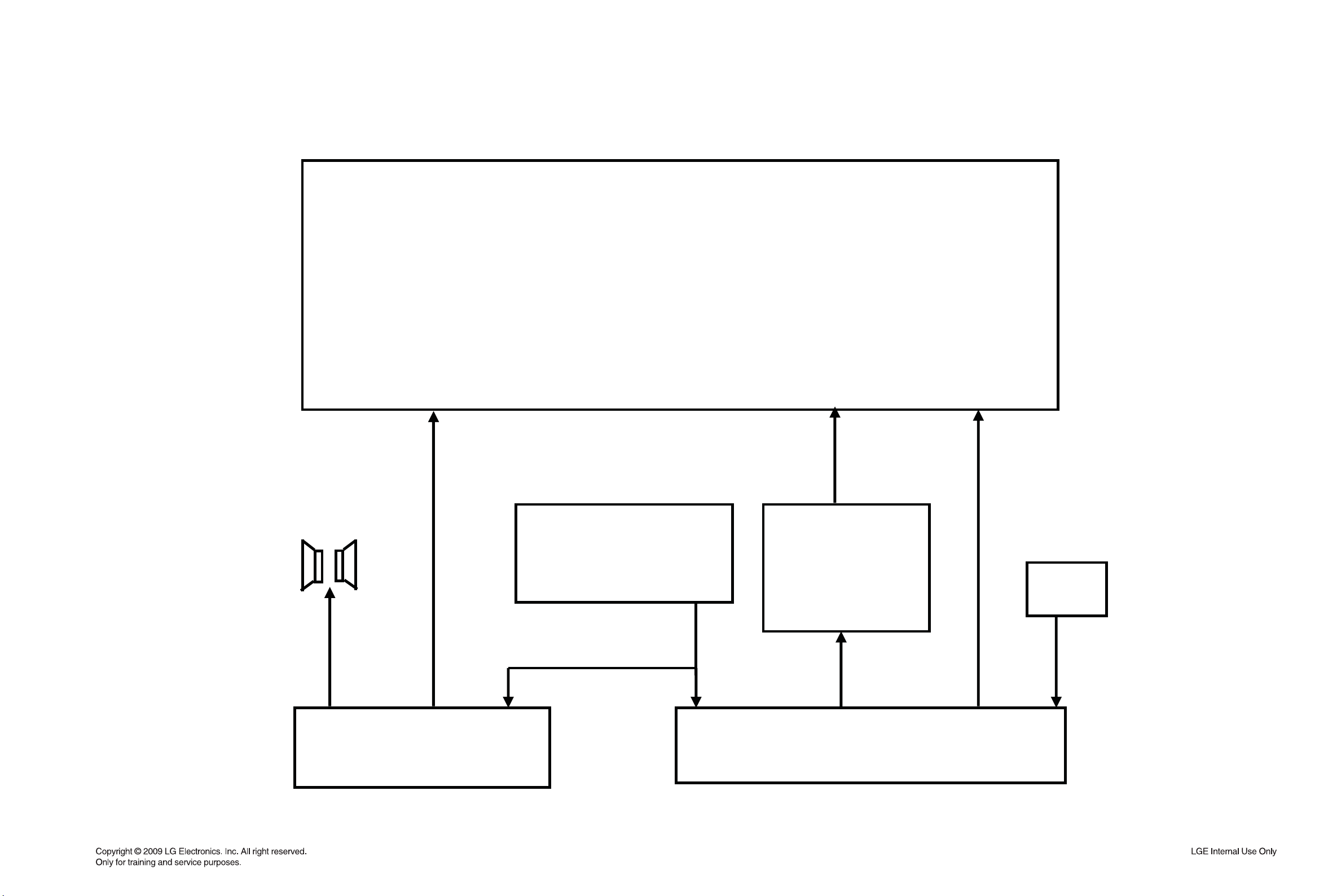
BLOCK DIAGRAM
TFT LCD
S
PL
SPL+/ -
SPR
SPR+/ -
STVL,CKV,OEV,OEH,STHL
,LED_EN,
Connecter
KEY1
KEY PAD
/ 2/ 3, SAM_KEY
R, G, B
BJT Amplifier
for RGB Vide
R, G, B
o
Connecter
IR
3. 3V, 5V, VGH/ L, VCOM, BL_VCC
3-3 3-4
Page 17

CIRCUIT DIAGRAMS
1. LCD TFT DRIVE CIRCUIT DIAGRAM
VGL
VDD1
VGH
C701
0.1uF
R719 0R
R720 0R
VCC_6312
R724
4.7K
IR
C720
100pF
89L_R 89L_G89L_B
R_IN G_IN
R707
10k
R718
NC
C702
0.1uF
75R/1%
CE709
10uF/16V
R727
+
VDD1
VDD1
R704
R705
10K
MOD
VGL_1
VGH_1
C703
0.1uF
IR1GND2VCC
R725
10R
R730
20K
1
R739
7.5K
NC
UNDLNR
R715
R714
10K
NC
CPH2
CPH3
GND
IR701
IR
3
C712
C724
0.1uF
10uF/10V
L7011.8uH
C713
100pF
V_BIAS AMP_VDDAMP_VDD AMP_VDD V_BIASV_BIAS
R731
470R
CE706
+
Vdc
10uF/16V
Q701
MMBT3904 LT1
2 3
R740
75R
R732
1M
R741
750K
C715
100pF
R_IN
ROUT
100R
R726
VCC_6312
R702
VDD1
0R
R711
1k/N C
75R/1%
CE710
B_IN
10uF/16V
W=20mil
R706 4.7R
VGH
R708 4.7R
STVR
TP702
1
W=15mil
W=20mil
W=15mil
W=15mil
W=15mil
W=20mil
L7021.8uH
C716
100pF
R734
470R
CE707
10uF/16V
Q702
MMBT3904LT1
2 3
R743
75R
BL_ISEN
BL_VCC+
GND
+
Vdc
STVL
CKV
UND
OEV
VCOM
LNR
MOD
OEH
STHL
STHR
CPH3
CPH2
CPH1
ROUT
GOUT
BOUT
AV5V
1
2
3
4
2pin 1 .25 mm SMD
B_IN
C717
100pF
R735
1M
BOUT
R744
750K
XP7 03
XP
VO
FB
G1
G2
C705
10uF/16V
NOTICE:
1.CPH1 for 10MHZ Signal ,and round about GND;
2.ROUT/GOUT/BOUT for Video RBG signal ,and round about GND;
3.VCOM for 7.8KHZ Vp-p 6 .4V Signal,and round about GND;
R728
R733
20K
+
1
R742
7.5K
VGL_1
VGH_1
27
XP701
1
1
GND
2
VCC
3
VGL
4
VGH
5
STVR
6
STVL
7
CKV
8
U/D
9
OEV
10
VCOM
11
VCOM
12
LR
13
MOD
14
OEH
15
STHL
16
STHR
17
CPH3
18
CPH2
19
CPH1
20
VCC
21
GND
22
VR
23
VG
24
VB
25
AVDD
26
AVSS
1
28
9" PANEL
HEADER 26 S MD0. 5 TOP
TOP Socket
C706 15pF
PANEL3V3
FB701
CE713
10uF/16V
VGH
ELN301
R703
10k
VX
+
+
R716
CE701
5.6k
10uF/16V
R721
10R
+12V_VOP
C707
2.2uF
VX
89L_VCOM
W=10mil
VGL
R709 47K
R712 0R
R722
10R
VX
+12V_VOP
C745
0.1uF
1
GND
2
VCC
3
VGL
4
VGH
5
STVR
6
STVL
7
CKV
8
U/D
9
OEV
10
VCOM
11
VCOM
12
LR
13
MOD
14
OEH
15
STHL
16
STHR
17
CPH3
18
CPH2
19
CPH1
20
VCC
21
GND
22
VR
23
VG
24
VB
25
AVDD
26
AVSS
R701 100k
-12V_VOP
U701A
-
2
1
+
3
NJM4558 OPA
8 4
+12V_VOP
VCOM DAC OP POWER
-12V_VOP
C708
2.2uF
C746
0.1uF
-12V_VOP
89P VCOM DAC OUTP UT
W=15mil
1
D701
1
2
2
PESD5V0S1BB/NC
VCOM
C709
22pF
22pF CLOSE XP701
R710 0/NC
R717
U701B
-
6
R713 0R/N C
7
+
5
8 4
NJM4558 OPA
0R
Close speaker.
VCC
VCC
75R/1%
FB702
FB703
R729
CE711
+
10uF/16V
CE714
10uF/16V
ELN301
ELN301
R736
20K
1
R745
7.5K
+
+
CE704
10uF/16V
C714
100pF
Q703
MMBT3904LT1
2 3
+
CE703
10uF/16V
L7031.8uH
R737
470R
CE708
+
10uF/16V
R746
75R
C747
C727
0.1uF
22pF
C748
0.1uF
BJT Am p lif ier f or R GB Video
G_IN
C728
100pF
R738
1M
GOUT
Vdc
R747
750K
V_BIAS
C726
22pF
AMP_VDD
V_BIAS
C725
22pF
PANEL3V3
VCC
FB704
R723 10R
ELN301
CE712
10uF/16V
PANEL3V3
C737 100pF
100pF
C721
C754
C757100pF/NC
C756
C755
100pF/NC
(+)
SPL2
(-)
SPL1
(+)
SPR1
(-)
SPR2
VDD1
W=20mil
+
CE702
C711
10uF/16V
0.1uF
AV5V
+
+
CE705
10uF/16V
89L_G
89L_R
VGH
VGL
33pF/NC
33pF/NC
C738 100pF
C740
C739 100pF
C741
TC701
C710
47uF/10V/NC
0.1uF
89L_B
VCC
33pF/NC
C743 100pF
C742
OEV
IR
CKV
STVL
33pF/NC
C730 100pF
C729 33pF
C731 100pF
C744
CPH1
STHR
STHL
OEH
33pF/NC
100pF
C732 100pF
C734 100pF
C733
C735
100pF/NC
100pF/NC
89L_VCOM
100pF
C736
SAM_KEY
LED_EN
KEY1
KEY2
KEY3
GND-KEY
SAM_KEY
C749 100pF
SPL2
SPL1
SPR1
SPR2
STVL
SAM_KEY 3
LED_EN 3
KEY1 3
KEY2 3
KEY3 3
GND-KEY 3
KEY1
LED_EN
KEY2
100pF/NC
C750 100pF
C753
C752 100pF/NC
CKV
OEV
OEH
STHL
100pF
C722
PANEL3V3
VGL
VGH
GND
BL_ISEN
BL_VCC+
KEY3
100pF/NC
C758
C718
100pF
VCC
100pF
C723
GND
SAM_KEY
GND-KEY
LED_EN
GND
CPH1
GND
89L_G
89L_B
89L_R
89L_VCOM
GND
VCC
VCC_6312
IR
GND
TC702
47uF/10V
Close XP704
100pF
C704
GND
GND
GND
C719
100pF
10
11
12
13
14
15
16
17
18
19
20
KEY3
KEY1
KEY2
GND
XP702
1
2
3
4
5
6
7
8
9
21
22
XP704
1
2
3
4
5
6
7
8
9
10
11
12
13
14
15
16
17
18
19
20
VCC_6312
100pF/NC
C759
3-5 3-6
Page 18

2. KEYPAD CIRCUIT DIAGRAM
SAM_KEY
SAM_KEY
SAM_KEY
SAM_KEY
SAM_KEY 2
SAM_KEY 2
LED_EN
LED_EN
LED_EN 2
LED_EN 2
KEY1
KEY1
KEY1 2
KEY1 2
KEY2
KEY2
KEY2 2
KEY2 2
KEY3
KEY3
KEY3 2
KEY3 2
GND-KEY
GND-KEY
GND-KEY 2
GND-KEY 2
C751
C751
100pF
100pF
R748 1K 1%
R748 1K 1%
R749 1.2K 1%
R749 1.2K 1%
R750 1.5K 1%
R750 1.5K 1%
R751 2K 1%
R751 2K 1%
R752 2.7K 1%
R752 2.7K 1%
R753 4.7K 1%
R753 4.7K 1%
R754 8.2K 1%
R754 8.2K 1%
R755 15K 1%
R755 15K 1%
KEY1
KEY1
K712
K712
1 2
1 2
KEY2
KEY2
K701
K701
K702 POWER
K702 POWER
K703
K703
K704
K704
K705
K705
K706
K706
K707
K707
K708
K708
1
1
K710
K710
K711
K711
1 2
1 2
K713
K713
1 2
1 2
1 2
1 2
1 2
1 2
1 2
1 2
1 2
1 2
1 2
1 2
1 2
1 2
1 2
1 2
1 2
1 2
TP703
TP703
1 2R769 39K 1%
1 2R769 39K 1%
POWER
POWER
LCD_MODE
LCD_MODE
RIGHT
RIGHT
LEFT
LEFT
COLOR
COLOR
BRIGHT
BRIGHT
DISPLAY
DISPLAY
LCD_OPEN
LCD_OPEN
GND-KEY
GND-KEY
LED_EN
LED_EN
R765
R765
4.7K
4.7K
K709
KEY3
KEY3
VCC
VCC
R756
R757
R756
R757
1K
1K
1K
1K
12
12
12
12
LED701
LED702
LED701
LED702
1
1
Q704
Q704
8050
8050
2 3
2 3
K709
1 2
1 2
R7581KR7591KR760
R7581KR7591KR760
12
12
12
12
LED703
LED704
LED703
LED704
LED_2COLOUR/NC
LED_2COLOUR/NC
1K/NC
1K/NC
12
12
LED705
LED705
LED_2COLOUR/NC
LED_2COLOUR/NC
R761
R761
1K/NC
1K/NC
12
12
LED706
LED706
LED_2COLOUR /NC
LED_2COLOUR /NC
R762
R762
1K/NC
1K/NC
12
12
LED707
LED707
LED_2COLOUR/NC
LED_2COLOUR/NC
12
12
R763
R763
1K/NC
1K/NC
LED708
LED708
12
12
R764
R764
1K
1K
LED709
LED709
12
12
R766
R766
1K
1K
LED710
LED710
12
12
R767
R767
1K
1K
LED711
LED711
12
12
R768
R768
1K
1K
LED712
LED712
3-7 3-8
Page 19

CIRCUIT VOLTAGE CHART
MEMO
MODE
PIN NO.
STOP PLAY
CE701
1 3.331 3.331
2 0 0
CE702
1 3.331 3.331
2 0 0
CE703
1 5.05 5.05
2 0 0
CE704
1 5.05 5.05
2 0 0
CE705
1 5.05 5.05
2 0 0
CE706
1 2.1 2.1
2 2.6 2.6
CE707
1 2.1 2.1
2 2.6 2.6
CE708
1 2.1 2.1
2 2.6 2.6
CE709
1 1.08 2.08
2 0.344 0.345
CE710
+ 1.08 1.08
- 0.344 0.344
CE711
+ 1.08 1.08
- 0.344 0.344
CE712
1 5.05 5.05
2 0 0
CE713
1 5.05 5.05
2 0 0
CE714
1 5.05 5.05
2 0 0
IR701
1 4.9 4.9
2 0 0
3 5.1 5.1
MODE
PIN NO.
STOP PLAY
U701
1 1.5 1.5
2 1.3 1.3
3 1.3 1.3
4 -9.5 -9.5
5 0 0
6 0.36 0.36
7 -7.8 -7.8
8 15 15
3-9 3-10
Page 20

PRINTED CIRCUIT BOARD DIAGRAMS
( TOP VIEW )
( BOTTOM VIEW )
3-11 3-12
Page 21

MEMO MEMO
3-13 3-14
Page 22

MAIN PART
MAIN ELECTRICAL TROUBLESHOOTING GUIDE
1. POWER (DC-DC CONVERTER) CIRCUIT
A. POWER
No power on
by ADAPTOR
YES
Is ADAPTOR
out 9V
YES
Is F1 OK.
YES
A
A
YES
NO
NO
Replace ADAPTOR
Replace F1
No power on
by BATTERY
YES
Is
BATTERY
OK?
YES
A
NO
Replace BATTERY
YES
Is
3.3V
OK?
YES
Replace U6
NO
Replace U8
No +3.3V No +5V No LCD powerNo +1.8V
3-15
Replace U8
Replace
XP6 or XP7
Page 23

MAIN ELECTRICAL TROUBLESHOOTING GUIDE
B. AUDIO OUT ABNORMAL
Audio out abnormal
YES
Check Audio jack & mode
YES
Check +5V
YES
Check signals from MPEG
YES
Replace IC(U11)
C. VIDEO OUT ABNORMAL
Video out abnormal
YES
Check Video jack & mode
YES
Check Video signals from MPEG
YES
Replace IC(U7)
D. PICTURE ABNORMAL
Picture abnormal
YES
Check the disc.
YES
Refer to SERVO part
YES
Check MPEG_CLK
Signal of MPEG part
YES
Check MPEG IC(U7)
(If OK)
YES(If OK)
E. DISC ERROR
Refer to SERVO part
Disc error
YES
Check Disc
YES
YES(If OK)
3-16
Page 24

MAIN ELECTRICAL TROUBLESHOOTING GUIDE
F. OPEN/CLOSE ABNORMAL
OPEN/CLOSE abnormal
YES
Check SW2 switch
YES
Check IC(U7) Pin 92
NO
Check the connectin of MD.
YES
Refer to SERVO part.
YES
Refer to SERVO part.
3-17
Page 25

MAIN ELECTRICAL TROUBLESHOOTING GUIDE
2. MPEG CIRCUIT
Power is on
Does
Logo appear
on the screen?
YES
Does the
Video of the DVD Disc
play properly?
YES
Does the
Video of the video CD
play properly?
NO
NO
YES
NO
Check power & clock.
YES
Is MPEG data
signal normal?
YES
Is error
signal normal?
Is MPEG data
signal normal?
NO
OK
NO
NO
Check CD/DVD DSP
output signal.
OK
Check MPEG decoder
input signal.
Check CD/DVD DSP
output signal.
YES
Check MPEG decoder
input signal.
Check CD/DVD DSP
output signal.
OK
OPTION
If included VCD function.
Does
the audio sound output
normally?
YES
END
NO
Is Clock normal?
YES
Does the audio
signal output from MPEG
decoder?
YES
3-18
Check MPEG decoder
input signal.
NO
Check clock signal
NO
Check clock signal
Page 26

MAIN ELECTRICAL TROUBLESHOOTING GUIDE
3. SERVO CIRCUIT
Focus on OK.
YES
Track on OK.
YES
NO
NO
Proper
signals on A, B, C, D
of MT1389LP
YES
Proper
FEO signal on
MT1389LP.
YES
Check IC(U8)
Proper
FEO signal on
MT1389LP.
YES
Properly
TRSO signal on
MT1389LP.
YES
NO
NO
NO
NO
Check connections between
MT1389LP and pick-up head.
Check the related circuit
on MT1389LP FEO signal.
Check the related
circuit on MT1389LP
Check the TRSO connection
on MT1389LP and motor dirver.
Disc is play?
YES
B
NO
T+ & T-
output properly.
YES
Check cable connection
on pick-up head.
Check the tracking control
amp circuit on motor driver.
3-19
Page 27

MAIN ELECTRICAL TROUBLESHOOTING GUIDE
B
YES
Normal
Audio output when
disc playback.
YES
Normal
IR. VFD & Front pannel
key functions.
YES
NO
NO
Aout_L, Aout_R signal
Proper
on MTK1389LP
YES
Check Audio filter,
amplify, mute circuit.
Commu-
nications between
IR.VFD Front pannel key &
MT1389LP & Front μ-com
is normally.
YES
NO
NO
Check Aout_L related circuit
Aout_R
NO
Check the related circuit of
Audio DAC.
Check communication
lines on MT1389LP
TEST END
NO
Check the cable connection
on Front pannel.
3-20
Page 28

MAIN ELECTRICAL TROUBLESHOOTING GUIDE
4. CHARGEING CIRCUIT
No turn on
Red LED
YES
Is L1 OK?
YES
Is IC(U3) OK?
YES
Is U1 OK?
YES
NO
Is 8.4V of XP1 RED Pin.
NO
Replace L1.
NO
Replace IC(U3).
NO
Replace U1.
Is U2 OK?
NO
Replace IC(U2).
3-21
Page 29

R50
180
Y2
27M
1 3
2
Crystal
XO
R48 100K
C54
27pF
C55
27pF
DETAILS AND WAVEFORMS ON SYSTEM TEST AND DEBUGGING
300mA
V18
300mA
R51
220
FB14
KLN301
CE8
100uF/6.3V
C63
0.1uF
V18
1. SYSTEM 27MHz CLOCK, RESET SIGNAL.
1-1. 1389LP main clock is at 27MHz(Y2)
1
1
FIG 1-1
1-2. 1389LP reset is active high.
3
2
FIG 1-2
3-22
R72
15K
R75 3.3K
R78
4.7K
3904
2
DV33
3
R73
D8
1N4148
3.3K
1
Q11
2 3
3904
1 2
1
Q12
2 3
R74
22K
CE10
22uF/25V
URST#
C92
0.22uF
RESET Circuit
Page 30

1-3. RS232 waveform during procedure(Downloading)
DV33
PAD2
PAD4
PAD1
PAD3
TXD
RS-232
RXD
SDC LK
DCLK
R125
150
C143
10pF
5
4
FIG 1-3
4 5
2. SDRAM CLOCK
6
FIG 2-1
6
3-23
Page 31

3. TRAY OPEN/CLOSE SIGNAL
GND
TRAY SW
TRIN
DV33
SW2
1
4
2
3
R44
10K
R46
1K
C51
0.1uF
FMSO
TRS O
SL+
R122 0
VOSP-
21
PGND
25
GND
36
VINTK
23
VCC2
24
VINSP
22
VOSP+
20
MGN D
19
VOTK-
18
SL-
T+
C125
1000pF
0.1uF
7
FIG 3-1
7
4. SLED CONTROL RELATED SIGNAL
8
9
FIG 4-1
3-24
U8 AM5898N
8 9
Page 32

5. LASER POWER CONTROL RELATED SIGNAL
F-
1
2
3
4
5
6
7
8
9
10
11
12
13
26
LDO1
LDO2
VR-DVD
T+
F+
T-
LD-DVD
R91 4.7
VR-CD
Q17
9012
1
2 3
L2
10uH
+
CE14
47uF/ 10V
12
+
CE13
47uF/10V
1 2
L3
10uH
R92 4.7
Q16
9012
1
23
S3.3V
MDI 1
LD-CD
T-
SP-
SP+
R121 10K
DMSO
FOSO
R120 0
GND
35
VCC1
10
VINSL+
12
VOSL+
14
MGN D
13
VINFC
11
VOSL-
15
MGN D
16
VOTK+
17
XP4
10
11
10
11
12
FIG 5-1
6. SPINDLE CONTROL WAVEFORM
15
14
13
12
U8 AM5898N
15
14
13
FIG 6-1
3-25
Page 33

7. FOCUS ON WAVEFORM
T-
FMSO
TRS O
SP- SL+
SP+
R121 10K
DMSO
FOSO
R120 0
R122 0
GND
35
VCC1
10
VINSL+
12
VOSP-
21
VOSL+
14
MGN D
13
PGND
25
GND
36
VINFC
11
VINTK
23
VCC2
24
VINSP
22
VOSL-
15
MGN D
16
VOTK+
17
VOSP+
20
MGN D
19
VOTK-
18
SL-
T+
C125
1000pF
0.1uF
T-
SP-
SP+
R121 10K
DMSO
FOSO
R120 0
0.1/ 1%
GND
35
VCC1
10
VINSL+
12
PVCC2
7
VOSL+
14
MGN D
13
PVCC1
6
S
IPK2
5
VOFC-
9
VINFC
11
VOFC+
8
VOSL-
15
MGN D
16
VOTK+
17
F+
F-
U8 AM5898N
16
16
17
17
18
18
FIG 7-1
8. TRACKING CONTROL RELATED SIGNAL(System checking)
U8 AM5898N
20
19
21
FIG 8-1
20 19 21
3-26
Page 34

9. 1389LP VIDEO OUTPUT WAVEFORM
0
TC3
470uF/6.3V/N C
P2
GND
1
coax
2
r
3
L
4
DET2
5
T1
6
DET
7
C169
1000pF
LCH
C168
1000pF
RCH
CVBS_OU T
D13
PESD5V0S1BB
1
1
2
2
D14
PESD5V0S1BB
1
1
2
2
0
TC3
470uF/6.3V/N C
P2
GND
1
coax
2
r
3
L
4
DET2
5
T1
6
DET
7
C169
1000pF
LCH
C168
1000pF
RCH
CVBS_OU T
D13
PESD5V0S1BB
1
1
2
2
D14
PESD5V0S1BB
1
1
2
2
22
FIG 9-1
22
10. 1389LP AUDIO OUTPUT WAVEFORM
23
FIG 10-1
23
3-27
Page 35

WIRING DIAGRAM
LCD PANEL
LCD & KEY PCB
BATTERY
USB PCB
DECK
MAIN PCB
3-28
Page 36

BLOCK DIAGRAMS
1. OVERALL BLOCK DIAGRAM-1
3-29
Page 37

2. OVERALL BLOCK DIAGRAM-2
-
DC 12V
INPUT
EARPHONE1
EARPHONE2
USB 2.0
AV OUT
+
Cell Protect Board
ADKEY
KEY3 KEY4
KEY3
KEY2
INPUT DECT
DC 12V
SPEAKER_L
SPEAKER_R
SPEAKER_L
L
R
SPEAKER_R
CVBS
KEY1
KEY2
PT2303
26PIN
GT6312
18PIN
IR
18PIN
L
R
JRC4558
OPA
L
R
KEY2
KEY3
KEY1
MPEG
MT1389LP TQFP 128
BATTERY:MCNIAR 3400mAh*2 7.4V
8OHM/1.5W
LCD PANEL AUO 8.5"
SPEAKER_R
KEY1
KEY9
KEY7 KEY8
ADKEY
KEY12 KEY13
KEY6
KEY11
KEY5
KEY10
EEPROM
8M bits
FLASH
8OHM/1.5W
20PIN
SPEAKER_L
20PIN
3.3V
3.3V
1.8V
3.3V
24PIN
MOTER DRIVER
1117
3.3V
AM5898
5V&3.3V OUT
DC 12V
INPUT
16*4M
SDRAM
3.3V
TOP3000S
3-30
Page 38

3. POWER BLOCK DIAGRAM
Charge
Discharge
LCD
Panel
Video
Audio
System
Servo
319
GT6
SW (9V in)
BAT Con
FET
Charge
V
5VA
FB
5
+
+5V
FB
3.3V
-5V
5V
-5V
Voltage Inverter
15V
P3V3
nse
Se
Thermist er
D5V
-10V
M5V
+5V
3.3V
V
7.5
V
1.8
-10V
V
3.3
15V
Vcc
LCD
M5V
V
5
D
P3V3
FB
5V
3.3V
1.8V
FB
Battery Charge Circuit
n
9V i
Charge Enable
AC/DC Adapter
BAT out
Divide Divide
se BAT
n
Se
DC
DC-DC
AM5898N
DC-DC
Standby
DC-DC
Standby
3-31
Page 39

4. SERVO BLOCK DIAGRAM
AL
X501
27MHz
X-T
U7
MTK1389LP
P-DVDPLAYER
ONE CHIP
FMSO,DMSO,FOSO,
,V1P4
TRSO,STBY
ALPC
IOA
MDI1,MDI2
CDLD(LD01),DVDLD(LD02)
PICK
DVD : A,B,C,D,RF
UP
F,RF
,
CD : A,B,C,D,E
TR+, TR-
FO+, FO-,
LIMIT
U8
SL-,SL+
ng
Moter
Steppi
AM5898N
Motor Driver
SP-,SP+
Moter
Spindle
OPO
OP+,OP-
3-32
Page 40

5. SYSTEM BLOCK DIAGRAM
3-33
Page 41

6. AV BLOCK DIAGRAM
3-34
Page 42

CIRCUIT DIAGRAMS
1. CHARGE GT6312 CIRCUIT DIAGRAM
C25
1000pF
12V_POWER
12
D7
1N4148
R36
51K
D6 SS24
1 2
BAT_CTL
CE39
100uF/16V
5
4
P1
Pws0 16-XX0
1000mA
BAT_OUT
R28
47K
SW_DET
213
SW1
IR
IR_OUT
A_MUTE_SW
GND
POWER I/F
AD_K
MPEG I/F
T_CTR L
DVD_SLEEP
P-
P+
C13
NC
VREF
C22
0.1uF
C6
0.1uF
12V_DVD#
R42 2K
R43
10K
F1
GLN101/2A
R30
47K
R38
22K
1
1 2
Q9
3904
2 3
D1 SS24
R25
2
G
ASM3401
1
FB1
GLN101/2A
FB2
GLN101/2A
NC
D3S
C19
Q7
0.1uF
1000mA
12V_DVD
FB4
C1
1000pF
C2
0.1uF
GLN101/2A
12V_DVD
CE4
100uF/25V
12V_POWER
1000mA
VCC_6312
12V/8.4VIN
C26
0.1uF
2
LED1
1 2
LEC03A
D2
SS24
TC5
47uF/25V
3
1
12V_POWER
C27
0.1uF
12
+
R23 470
R24 470
R31
220K
AD_PR
R40
51K
C3
0.1uF
RED
GREEN
VCC_6312
R32
100K
C4
1000pF
12V_DVD#
VCC_6312
SW_DET
R2
10K
R13
2K
B
1
1
B
3904
12V_POWER
12V_DVD#
R33
51K
C
Q2
3904
E
2 3
E
3906
Q3
C
3 2
Q5
BAT54C
RED
GREEN
SYS_EN
T_CTR L
PWM
SP_MUTE
R1
R3
10K
10
R5
51
C
B
1
E
2 3
R15
10K
D5
1
3
2
C232
0.1uF
R232
C23
0.1uF
2
3
5
4
6 1
R37
22K
R231
100
ASM3401
Q8
2
C5
1000pF
D3S
G
1
SYS_EN
BAT_OUT
BAT_CTL
+
AD_U
AD_I
U1
AO4803A
1
S1
2
G1
3
S2
G24D2
R16
3.6K
2
CE2
47uF/10V/ NC
1K
10
1
2
3
4
5
6
7
8
9
VIN
D1
D1
D2
U2
HT7150
TC_SET
DO
RED
GREEN
PWM
PWMT
RST
GND
SAM_U
SAM_I
8
7
6
5
PWM
GND
1
U3
GT6312A
VOUT
CHG_CTL
3
47uF/10V
SC_SET
CC_SET
DC_CTL
VREF
OSC
VDD
SAM_V
SAM_T
1 2
CE3
FB
T_CTRL
R240
20K
L1
33uH/2A
D3
C7
SS24
0.1uF/ NC
IR_OUT
20
SW_DET
19
IR
18
PANEL_SW
17
VREF
16
A_MUTE_SW
15
R34 9.1K/1%
14
13
AD_KEY
12
AD_PR
11
VCC_6312
C8
1000pF/NC
AD_U
C11
1000pF
FB3 KLN301
15mA
C16
0.1uF
C24
0.1uF
10K
CE40
100uF/16V
150K/1%
VCC_6312
1R239
B
R8
R11
51K/1%
VCC_6312
R351K
R39
10K/1%
E
Q34
C
3906
3 2
P+P+
AD_I P-
AD_K
T
R9
NC
R12
NC
C17
1000pF
R244
36K
VCC_6312
C18
0.1uF
VCC_6312
Q36
3904
C10
0.1uF
2 3
1K
R10
0.15/1%
C20
0.1uF
R24310K
R26
1K
DVD_SLEEP
C9
0.1uF
C21
10uF/10V
R233
0.15/1%
R234
0.15/1%
T
C12
NC
R27
1K
2
U4
1
KA431
3
R4
1
12V/8.4VIN
VCC_6312
12V_DVD
PANEL_SW
SP_MUTE
XP1
3
2
1
CONN3P1.25C
IR 8
IR_OUT 4
A_MUTE_SW 7
GND 4,5,6,7,8
AD_K 8
12V/8.4VIN 5,7
VCC_6312 8
12V_DVD 4
PANEL_SW 4
SP_MUTE 7
T_CTRL 8
DVD_SLEEP 4
3-35 3-36
CHARGE GT6312
Friday, December 05, 2008
Page 43

2. MPEG CIRCUIT DIAGRAM
3.3V
DV33
FB10
KLN301
FB12
KLN301
DV33
KLN301
3.3V
C74
0.1uF
XP2
5 6
CON4P1.25XP
FB5
KLN301
C40
10uF/10V
C48
10uF/10V
FB13
C56
6800pF
U6 AZ1117D-ADJ-TO252
3
IN
USB 2.0 I/F
4
3
2
1
CE9
47uF/10V
KLN301
CE8
300mA
V18
FB6
KLN301
FB8
KLN301
XI
R49
180
C54
27pF
C34
0.1uF
C37
0.1uF
RFV18-1
C35
1000pF
RFV18-2
C38
1000pF
R48 100K
Y2
27M
1 3
2
Crystal
300mA
V18
V18
C63
0.1uF
V1P4
F2
3
Q10
FUSE(500MA)
8050
1
R62
910
12V_DVD
FOO
TRO
47K
FMO
DMO
10K
2
VCC_5V
DV33
R246
10K
C236
1000pF
AVDD3 3
RFV18-2
RFVDD3
MDI 1
LDO1
LDO2
DV33 DV33
R76
10K
C93
1000pF
DV33
12
C33
C32
0.1uF
C41
0.1uF
C49
0.1uF
C57
0.1uF
ADJ
1
C233
C86
15pF/NC
0.1uF
OSOF
OSRT
F
SM
O
S
MD
O
C87
330pF
OUT
C42
1000pF
C50
1000pF
12
+
R56
R57
1000pF
RFVDD3
AVDD33
AADVDD
CE6
100uF/6.3V
2
C234
15pF/NC
C88
330pF
R51
220
0
0
+
C89
0.1uF
CE5
100uF/6.3V
RFVDD3
AVDD33
FB14
USBM
USBP
AADVDD
100uF/6.3V
R55
100
R67 47K
R68
R69 15K
R70
C90
0.015uF
RFV18-1
RFV18-2
C55
27pF
R77
10K
C94
1000pF
DV33
R50
180
C
B
A
R60 0
D
F
R63 0
E
R65 15K
R66 0
DV33
R71 5.1K
C91 NC
V18
DVD_KEY3
DVD_KEY1
DVD_KEY2
XO
RFV18-2
RFVDD3
XI
XO
V20
V1P4
AVDD33
DMO
FMO
STBY
IOA
TRO
FOO
LIMIT
USBP
USBM
FB7 KLN301
FB9 KLN501
FB11 KLN301
OPO
R52 0
OP-
R53 0
U7
1
RFA
2
RFB
3
RFC
4
RFD
5
RFE
6
RFF
7
AVDD18_2
8
AVDD33_1
9
XTAL I
10
XTAL O
11
AGND33
12
V20
13
V14
14
REXT
15
MDI 1
16
MDI 2
17
LDO1
18
MDI LDO 2
19
AVDD33_2
20
DMO
21
FMO
22
TRAY _O PEN
23
TRAY _C LOSE
24
TRO
25
FOO
26
PG/GPIO2
27
USB_DP
28
USB_DM
29
VDD33_USB
30
VSS33_USB
31
PAD_VRT
32
VDD18_USB
ADACVDD
APLLVDD3
C45
0.1uF
RFV18-1
RFO
C78 220pF
124
125
RFIP
RFIN/OPOUT
ADACVDD
APLLVDD3
DACVDD3
DACVDD3
C46
C47
1000pF
1000pF
C61
C59 0.1uF
C60 10uF/10V
C62 0. 1uF
CE7
+
100uF/6.3V
10uF/10V
1 2
TP7
C64 1500pF
1
ADACVDD
AVCM
RFV18-1
AL
AR
APLLVDD3
119
122
121
116
123
120
118
117
AVCM
AGND18
AVDD18_1
APLLCAP
AL/GPIO1
AR/GPIO0
ADACVSS
ADACVDD 2
ADACVDD 1
89L_B
VCOMO
89L_R
DVD_SLEEP
AADVDD
114
110
115
109
108
112
113
111
R
AADVSS
AADVD D
APLLVDD
ADVCM/ GPIO20
AKIN1/GPI O21/Audio_mute
AKIN2/GPI O19/Audio_mute
C36
1000pF
C39
1000pF
C43
10uF/10V
C58
120pF/NC
C44
0.1uF
C79 1uF
128
127
126
RFG/OPINP
RFH/OPINN
MT1389LP
GPIO3/IN T#33GPIO434GPIO635SF_CS_36SF_DO37SF_DI38SF_CK39UP1_6/SCL40UP1_7/SDA41ICE42PRST#43IR44RD045RD146RD247RD348RD449DVDD3350RD551RD652RD753DVDD1854DQM055RD1556RD1457RD1358RD1259DVSS3360RD1161RD1062RD963RD8
URST#
SF_CK
DQ0
DQ1
DQ2
DQ3
DQ4
DVD_KEY1
DVD_KEY2
DVD_KEY3
VGH_C
SF_DO
SF_DI
SF_CS
1
1
1
TP6
TP3
TP5
IR_OUT
C95
18pF
DQ5
DQ6
DV33 V18
DQ7
C30
0.1uF
CVBS
FB15 KLN 501
DACVDD3
DACVDD3
89L_G
104
106
105
107
B
G
DACVDDA
DACVDDB
DQM0
DQ15
DQ14
C65
180pF
103
CVBS
DQ13
GND
FS
102
101
FS
DACVSSC
DQ12
V20
C28
10uF/10V
SW2
4
3
TRAY SW
CPH1
KLN501
STHL
OEH
DACVDD3
FB16
99
97
98
100
VREF
DACVDDC
HCK/GPIO18
HSTL/GPI O17
SPDIF/ GPIO12
64
DQ10
DQ11
DQ8
DQ9
48-PUS006-XX0GA
1
2
R46
C76
0.1uF
VOE/GPIO15
HOE/GPIO16
VCK/GPIO14
VSTU/GPIO13
HSTR/11
LR/GPIO10
DVDD18
UD/GPIO9
VSTD/GPIO8
GPIO7/CKE
DVDD33
RA10
DVSS18
RAS#
CAS#
RWE#
DVDD33
RA11
RCLK
DQM1
MT1389L/SMD
MT1389L
V1P4
C29
10uF/10V
C31
0.1uF
RF Refe rence
R44
10K
1K
0.1uF
R54
560/1%
C77
1000pF
V18
96
95
94
93
92
91
90
89
88
87
86
RA3
85
RA2
84
83
RA1
82
RA0
81
80
BA1
79
78
BA0
77
76
75
74
RA4
73
RA5
72
RA6
71
RA7
70
RA8
69
RA9
68
67
66
65
DV33
TRI N
C51
DV33
OEV
CKV
STVL
TRI N
TXD
RXD
MA3
MA2
MA1
MA0
MA10
BA1
BA0
RAS#
CAS#
WE#
MA4
MA5
MA6
MA7
MA8
MA9
MA11
DCLK
DQM1
C75
33pF/NC
BL_EN
LED_EN
SF_CS
SF_DO
SF_DI
SF_CK
S-FLASH
VCOMO
STVL
CKV
OEV
OEH
STHL
LCD
CPH1
89L_R
89L_G
POWER
CONTRL
AL
AR
IR_OUT
BA0
BA1
MA[0..11]
DQ[0.. 15]
DQM[0..1]
DCLK
CAS#
RAS#
WE#
12V_DVD
BL_EN
LED_EN
PANEL_SW
V1P4
V20
OPO
OP-
LIMIT
IOA
LDO1
LDO2
A
B
C
D
E
F
RFO
MDI 1
STBY
TRS O
DMSO
FOSO
FMSO
89L_B
VGH_C
DVD_SLEEP
GND
AMP5V
LCD PANEL_SW
CLOSE: L
C68
0.1uF
C82
0.1uF
C52
0.1uF
R45
100K
C69
1000pF
C83
1000pF
RS-232
DV33
OPEN: H
C53
100pF
C70
0.1uF
C84
0.1uF
PAD1
PAD2
PAD3
PAD4
R47
100
C71
1000pF
C85
1000pF
PANEL_SW
C72
0.1uF
C73
1000pF
1
3
2
U5
MH248
DV33
C66
C67
0.1uF
1000pF
V18
C80
C81
0.1uF
1000pF
TP2
1
DV33
RXD
TXD
VCC_5V
3.3V
CVBS
FLASH
MA[0..11] 6
DQ[0..15] 6
DQM[0..1] 6
DCLK 6
CAS# 6
RAS# 6
WE# 6
12V_DVD 3
LED_EN 8
V1P4 5
V20 5
OPO 5
OP- 5
LIMIT 5
IOA 5
LDO1 5
LDO2 5
A5
B5
C5
D5
E5
F5
RFO 5
MDI 1 5
STBY 5
TRSO 5
DMSO 5
FOSO 5
FMSO 5
SF_CS 6
SF_DO 6
SF_DI 6
SF_CK 6
VCOMO 8
STVL 8
CKV 8
OEV 8
OEH 8
STHL 8
CPH1 8
89L_R 8
89L_G 8
89L_B 8
VCC_5V 5,7
3.3V 5,6,8
CVBS 7
AL 7
AR 7
IR_OUT 3
BA0 6
BA1 6
VGH_C 3
DVD_SLEEP 3
BL_EN 8
GND 3,5,6,7,8
PANEL_SW 3
MEMORY
SERVO I/F
R72
15K
R75 3.3K
R78
4.7K
3904
R73
3.3K
3904
1 2
1
2 3
Q12
2 3
1
Q11
D8
1N4148
R74
22K
CE10
22uF/25V
URST#
C92
0.22uF
RESET Circuit
DVD_KEY1
DVD_KEY2
DVD_KEY3
DVD_KEY 1 8
DVD_KEY 2 8
DVD_KEY 3 8
3-37 3-38
MT1389LP
Friday, December 05, 2008
Page 44

3. DC-DC & MOTOR & OPU CIRCUIT DIAGRAM
A/a
24
D/d
23
RF
22
21 SW
20
B/b
19
C/c
18
F
VCC-PD
17
16
VC-PD
Gnd-PD
15
E
14
13
VR-DVD
VR-CD
12
MD
11
LD-DVD
10
Gnd-LD
9
8
LD-CD
Gnd-LD
7
6
T+
5
FF+
4
3
TNC
2
1
NC
TopRay
TOP3000
XP4
24
23
22
21
20
19
18
17
16
15
14
13
12
11
10
9
8
7
6
5
4
3
2
1
25
26
CONN24P0.5TOP
100uF/ 6.3V/NC
VCC_5V
FB17
12
KLN301
+
Very Important to
reduce Noise
L2
10uH
23
L3
Q16
R91 4.7
R92 4.7
2 3
Q17
A
D
RFO
IOA
B
C
E
PUH5V
V20
C102 0. 1uF
F
C103 100 0pF
VR-DVD
VR-CD
MDI 1
LD-DVD
LD-CD
TFF+
T+
C99
0.1uF
C100
1000pF
10uH
OPU Protection
R96
10K/N C
CE16
R98 0/NC R99 0/NC
LDO2
23
Q20
1
3906/NC
CE11
100uF/ 16V
9012
1
9012
1
CE17
100uF/6.3V/NC
LDO1
R79 100K
Q14
2SK3018
2
G
R85
0
C104
NC
+
CE13
47uF/1 0V
1 2
12
+
CE14
47uF/1 0V
R97
10K/NC
C
E
S
3 1
1
R80 10K
3904
Q13
B
1
2 3
S
D
D
3 1
S3.3VS3.3V
23
Q21
3906/NC
R81
R83 100K
2
G
2SK3018
Q15
R86
0
C105
NC
LDO1
10K
LDO2
S3.3V
VCC_5V
IOA
R94
51K
R93
27K
SP-
SP+
SP-A
XP5
3
4
CONN2P1.25C
12V/8.4VIN
2
1
3906
3
M5V
Q18
R95
6.8K
1
2
1
CONN4P1.25C
4
5
3
6
2
1
XP3
R88 NC
R89 0
SL-
SL+
C107
NC
CT1
32
Q19
3904
SP-A
SP+
LIMIT
R84 10K
R87
1
R90 10K
C108
NC
3.3V
VCC_5V
VCC_5V
C110
0.1uF
C101
0.1uF
C106
0.1uF
C96 100pF
C97
C98
0.1uF
D9
BAT54C
FB18
KLN301
GLN101/2A
KLN301
2
1
FB66
FB20
100pF
C115
0.1uF
R82
10k
OP-
OPO
3
C109
0.1uF
0.1uF
C112
DV33
C116
1000pF
S3.3V
C111
1000pF
TC2
47uF/10V
12
CE18
+
47uF/1 0V
S3.3V
12
+
CE12
47uF/10V
5VA
M5V
5VA
3.3V
GND
VCC_5V
12V/8.4VIN
V20
V1P4
STBY
TRSO
DMSO
FOSO
FMSO
OP-
OPO
LIMIT
LDO1
LDO2
IOA
A
B
C
D
E
F
RFO
MDI 1
SERVO I/F
5VA 8
3.3V 4,6,8
GND 3,4,6,7,8
VCC_5V 4, 7
12V/8.4VIN 3, 7
V20 4
V1P4 4
STBY 4
TRSO 4
DMSO 4
FOSO 4
FMSO 4
OP- 4
OPO 4
LIMIT 4
LDO1 4
LDO2 4
IOA 4
A4
B4
C4
D4
E4
F4
RFO 4
MDI 1 4
3.3V
GLN101/2A
FB22
C123
0.1uF
12
CE20
+
220uF/ 10V
L5
47uH/1 .3A
12V/8.4VIN
D10
SS24
100uF/25V
12V/8.4V IN
1 2
CE21
D
S
2 3
12
+
M5V
R105 2K/1%
R107
Q22
750
AO3409
G
1
C127
C128
0.1uF
1000pF
C132
1000pF
R100 10K
R102 10K
R104 1.2K/1%
R106 33
C120
1000pF
R110
680K
R116 0.1/1%
M5V
C133
0.1uF
F+
F-
FOSO
DMSO
SP+
SP-
T-
R111 0
R120 0
R121 10K
VCC_5V
FB21
R101 20K
R103 10K
U8
AM5 89 8N
1
EN2
2
CT2
3
COMP2
4
SW2
5
IPK2
6
PVCC1
7
PVCC2
8
VOFC+
9
VOFC-
35
GND
10
VCC1
11
VINFC
12
VINSL+
13
MGN D
14
VOSL+
15
VOSL-
16
MGN D
17
VOTK+
BIAS
MUT E
EN1
CT1
COMP1
SW1
IPK1
PGND2
PGND1
GND
PGND
VCC2
VINTK
VINSP
VOSP-
VOSP+
MGN D
VOTK-
34
33
32
31
30
29
28
27
26
36
25
24
23
22
21
20
19
18
V1P4
STBY
R108 10K
CT1
C122 68 pF
R114 10K
R117 0
R122 0
C119
C124
0.1uF
SLSL+
T+
0.1uF
C125
1000pF
TRSO
FMSO
12V/8. 4VIN
R109 1.2K/1%C121 68pF
R112 100
R115 680K
R118 0.1/1%
M5V
12V/8.4V IN
R119
750
R113 3.6K/1%
23
1
G
1000pF
C126
1 2
S
Q23
AO3409
D
D11
SS24
12V/8.4 VIN
L6
47uH/2 A
220uF/ 10V
CE23
KLN301
C117
0.1uF
C118
1000pF
FB23
GLN101/2A
12
+
C131
0.1uF
12
+
CE19
47uF/1 0V
C129
0.1uF
+5V
VCC_5V
12
+
CE22
C130
1000pF
100uF/16V
DC-DC&MOTOR&OPU
Friday, December 05, 2008
3-39 3-40
Page 45

4. SDRAM & FLASH CIRCUIT DIAGRAM
SD33
R123 10K
R124 10K
DCLK
R125
150
BA0
R126
BA1
R127
RAS#
1
CAS#
2 7
WE#
3 6
4 5
SD33
R129
15K/NC
R133
3.3K/NC
SDRAM
U9
ESMT M12L64164A-7T
MA0
23
A0
SDCKE
C135
68pF
DCS#
SDCLK
C143
10pF
33
33
RN1
33*4
B
1
C
E
2 3
8
R130
10K/N C
Q25
3904/NC
DBA0
DBA1
DRAS#
DCAS#
DWE#
G
2
FLASH_3.3V
31
D
Q24
2SK3018/NC
S
R128
39
MA1
MA2
MA3
MA4
MA5
MA6
MA7
MA8
MA9
MA10
MA11
DBA0
DBA1
SDCLK
SDCKE
DCS#
DRAS#
DCAS#
DWE#
DQM0
DQM1
24
A1
25
A2
26
A3
29
A4
30
A5
31
A6
32
A7
33
A8
34
A9
22
A10/AP
35
A11
20
BA0/A13
21
BA1/A12
38
CLK
37
CKE
19
CS
18
RAS
17
CAS
16
WE
15
DQML
39
DQMH
36
NC1
40
NC2
54
VSS
41
VSS
28
VSS
FLASH_3.3V
DQ0
DQ1
DQ2
DQ3
DQ4
DQ5
DQ6
DQ7
DQ8
DQ9
DQ10
DQ11
DQ12
DQ13
DQ14
DQ15
VCC
VCC
VCC
VCCQ
VCCQ
VCCQ
VCCQ
VSSQ
VSSQ
VSSQ
VSSQ
SF_CS
SF_DO
R132 10K
FLASH_3.3V
DQ0
2
DQ1
4
DQ2
5
DQ3
7
DQ4
8
DQ5
10
DQ6
11
DQ7
13
DQ8
42
DQ9
44
DQ10
45
DQ11
47
DQ12
48
DQ13
50
DQ14
51
DQ15
53
SD33
1
14
27
SD33
3
9
43
49
6
12
46
52
S-FLASH
U10
1
CS#
2
DO
3
WP#
VSS4DI
AT25FS040/EN25B16
R134 NC
R135
3.3V SD33
FB24
KLN301
12
+
CE25
47uF/10V
SD33
C136
0.1uF
SD33
C144
1000pF
8
VCC
7
HOLD#
6
CLK
5
SF_CS
10K
C137
0.1uF
C145
1000pF
FLASH_3.3V
C151
0.1uF
R131 10K
SF_CK
SF_DI
C134
0.1uF
C138
0.1uF
C146
1000pF
C139
0.1uF
C147
1000pF
FLASH_3.3V
C140
0.1uF
C148
1000pF
C141
0.1uF
C149
1000pF
C142
0.1uF
C150
1000pF
3.3V
DCLK
CAS#
RAS#
WE#
BA0
BA1
MA[ 0. .1 1]
DQM[0..1]
DQ[0..15]
SF_CK
SF_CS
SF_DI
SF_DO
GND
DRAM
S-FLASH
3.3V 4,5,8
DCLK 4
CAS# 4
RAS# 4
WE# 4
BA0 4
BA1 4
MA[0 .. 11] 4
DQM[0..1] 4
DQ[0..15] 4
SF_CK 4
SF_CS 4
SF_DI 4
SF_DO 4
GND 3,4,5,7,8
P901
6
GND
5
GND
USB CONN-A x 1
USB5V
4
1
VBus_1
D-_1
D+_1
GND_1
1
2
3
4
USBM-
D901
PRTR5V0U2X
USBP+
2 3
USBMUSBP+
C902
0.1uF
USB5V
C904
1000pF
FB901 KLN301
C900
C903
15pF
10uF/ 10V
C901
15pF
R901
15K/N C
R902
15K/NC
XS9 00
4
3
2
1
3-41 3-42
SDRAM & FLASH
Friday, December 05, 2008
Page 46

5. AUDIO & VIDEO OUTPUT CIRCUIT DIAGRAM
R136 24K
C152 100pF
+15VM
AGND
CE27
AR4
AL
4
W=15mil
VGH
12V/8.4VI N
22uF/25V
W=15mil
CE31
22uF/25V
W=15mil
R139
4.7K
R151 4.7K
R162 10
AGND
AGND
FB27
KLN301/N C
CE32
100uF/25V
C156
1000pF
C161
1000pF
+15VM
AGND
R140 3.9K
AGND
R152 3.9K
AGND
VCC_5V
R141
C155
1000pF
R153
C160
1000pF
FB19
KLN301
R169
AGND
1K
4.7K
4.7K
R146 24K
CE34
100uF/16V
+15VM
W=20mil
R190
R174
C184
PGND
C182
0.1uF
0.1uF
R171
1K
8
IN+
IN+9Vref10IN-11OUT2-12VDD13OUT2+14GND15HP-IN
1K
R193
C177
W=80mil
W=20mil
C187
R172
18K
PGND
R192
18K
AGND
PGND
R182
C183
2.2uF/ 16V
1
2.2uF/16 V
C180
1000pF
RP1
C20K
10K
R181
MR1
ML1
R183
10K
AGND
AGND
AGND
C186
1000pF
2.2uF/1 6V
PGND
84
3
+
2
-
58N58N
C157 100pF
84
5
+
6
-
U14B
AS4558M
R160
0/NC
AGND
AMP5V
C173
12
1000pF
+
AMP5V
75K
6
5
7
IN-
GND
OUT1-
U11
PT2303-S(L)(SOP16)
AMP5V
75K
C153
0.1uF
1
U14A
AS4558M
C158
1000pF
7
R158
C162
0.1uF
C174
0.1uF
4
VDD
AGND
AGND
AGND
3
OUT1+
2K
C181
1uF/10V/ NC
R184
680K/NC
HPEARSW
W=15mil
R144 1K
3904
W=15mil
R157 1K
3904
A_MUTE_SW
D20
12
1N4148/N C
CE26
R138 330
22uF/25V
A_MUTE
CE30
R150 330
22uF/25V
C163
10uF/10V
SP_L-
R29
A_MUTE
SP_R-
VCC_5V
AGND
SP_L+
SP_R+
0
VGL
AGND
1
2
GND
SHUTDOWN
16
Q26
Q29
220uF/10V
A_MUTE
220uF/10V
1
ML1
1
AGND
CE35
MR1
AGND
CE36
2 3
R156
100k
2 3
AGND
AGND
R143
100K
AGND
AGND
R179
1K
R188
1K
AGND
100pF
AGND
AGND
AGND
C154
100pF
C159
CVBS
R167
75/1%
1000pF
C185
1000pF
FB25
KLN501
FB26
KLN501
R176
R178
R185
R186
C170
100pF
RCH
LCH
C166
100pF
L7
1.8uH
33
33
33
33
C171
100pF
FB28 KLN501
FB29 KLN501
FB32 KLN501
FB33 KLN501
C172
47pF
330pF/N C
MROU T1
MROU T2
MLOU T2
MLOU T1
C167
AMP5V
R166
10K/NC
D15
1
1
2
PESD5V0S1BB
2
AGND
R147
100
A_MUTE_SW
R165
VCC_5V
R142
100K
CE29
47uF/10V
TC3
470uF/6. 3V/NC
3
R155
R145 1K
R159
10K
0
2
D12
BAT54S
1
3906
20K
RCH
LCH
CVBS_OUT
C168
1000pF
Q27
R161
100K
AGND
CE28
100uF/16V/ NC
23
1
Q28
2
1
1
2
AGND
A_MUTE
3906
3
1
R154
10K
Q30
3904
2 3
C169
1000pF
D13
1
D14
1
1
2
2
PESD5V0S1BB
2
HPEARSW
C176
0.1uF
1
6
7
3
5
4
2
PESD5V0S1BB
GND
T1
DET
r
DET2
L
coax
P2
R170
10K
SP_MUTE
R149
100K
VGL
VGH
VGL
VCC_5V
GND
CVBS
AL
AR
A_MUTE_SW
SP_MUTE
12V/8.4VI N
MPEG I/F
SP_LSP_L+
SP_RSP_R+
3
D17
R173
1M
1N4148
1 2
EARPHONE HPEARSW
IN H
OUT L
MLOU T2
POWER I/F
D16
BAT54C
MRO UT2
C188
1000pF
AMP5V
2
1
R168
30K
AMP5V
C178
1000pF
R189
30K
VGH 8
VGL 8
VCC_5V 4,5
GND 3,4,5,6,8
CVBS 4
AL 4
AR 4
A_MUTE_SW 3
SP_MUTE 3
12V/8.4VIN 3,5
SP_L- 8
SP_L+ 8
SP_R- 8
SP_R+ 8
MROU T1
MLOU T1
C179
1000pF
1
C189
1000pF
2
W=15mil
W=15mil
D21
1
2
PESD5V0S1BB
1
GND
6
T1
7
DET
3
r
5
DET2
4
L
2
1
2
1
6
7
3
5
4
2
PESD5V0S1BB
coax
D19
P3
1
2
PESD5V0S1BB
GND
T1
DET
r
DET2
L
coax
P4
D18
1
1
2
PESD5V0S1BB
2
1
D22
1
2
2
3-43 3-44
AUDIO&VIDEO OUTPUT
Friday, December 05, 2008
Page 47

6. PANEL CIRCUIT DIAGRAM
VCOMO
SP_LSP_L+
SP_RSP_R+
VGH
BL_EN
VGL
LED_EN
DVD_KEY 1
DVD_KEY2
DVD_KEY3
T_CTRL
IR
VCC_6312
VGH_C
PANEL T-CON I/F
AD_K
VCC_5V
3.3V
5VA
TO SERVO
STVL
CKV
OEV
OEH
STHL
CPH1
89L_R
89L_G
89L_B
GND
VCOMO 4
STVL 4
CKV 4
OEV 4
OEH 4
STHL 4
CPH1 4
89L_R 4
89L_G 4
89L_B 4
SP_L- 7
SP_L+ 7
SP_R- 7
SP_R+ 7
VGH 7
BL_EN 4
VGL 7
LED_EN 4
DVD_KEY1 4
DVD_KEY2 4
DVD_KEY3 4
T_C TRL 3
GND 3,4,5,6,7
IR 3
VCC_6312 3
VGH_C 3
AD_K 3
VCC_5V 4,5 ,7
3.3V 4,5, 6
5VA 5
NOTICE:
BL_EN: H for BL ON;
BL_EN: L for BL OFF;
BL_EN
12V_POWER
FB47
+5V
R194
47K
R197
10K
KLN501/N C
C202
10uF/16V/ NC
DC_IN
C203
0.1uF/ NC
DC_IN: H for BL_AMP 80mA;
DC_IN: L for BL_AMP 65mA;
FB40
DC_IN
C199
10uF/10V
W=40mil
KLN301
C237
22uF10V
DC_IN
R205
BL_VCC+
C196
1000pF
R196
100K/NC
C197
0.1uF
6
10K
5
4
Q33
2SK3018/NC
R206
100K/NC
2
VDD
VOP
EN
U12
MP1488
L9
10uH/500m A
LX
GND
FB
R202
1 3
5VA
FB34
KLN301/NC
3.3V
FB35
KLN301
W=40mil
D23
1 2
MBRX140
C198
2.2uF/ 16V
1
2
R198
3
10K
225mA
BL_VCC +
BL_ISEN
T_C TRL
PANEL3V3
C192
0.1uF
R241 10K
C193
1000pF
1
CE37
100uF/6. 3V
Q35
3904
2 3
R242
0/NC
STVL
CKV
OEV
OEH
SP_L+
SP_LSP_R+
SP_R-
4
5
6
3
7
2
1
8
RN2
33*4
PANEL3V3
VGL
VGH_OUT
STHL
AD_K
LED_EN
C190
100pF
C194
100pF
R195 33
FB36
FB37 KLN501
FB38 KLN501
FB39
2.5mA
FB41 KLN501
FB42 KLN501
FB43 KLN501
FB54 KLN501
FB55 KLN501
FB56 KLN501
FB57 KLN501
FB44 KLN501
FB45 KLN501
C191
100pF
KLN501
KLN501
C195
100pF
KLN501
GND
PANEL3V3_C
GND
STHL1
FB58
KEYO
LED_ENO
STVL1
CKV1
OEV1
OEH1
GND
GND
GND
XP6
1
2
3
4
5
6
7
8
9
10
11
12
13
14
15
16
17
18
19
20
21
22
W=40mil
1/NC
R203
1
W=40mil
R204
NC
VGH_C
VCOMO1
Q38
VGH VG H_OUT
AGND
R238
20K
C235
0.1uF/ NC
R236
20K
1
R235
0/NC
D27
1N4148
2
2
1
R245
100K/NC
AGND
3906
3
1
R237
20K
Q37
3904
2 3
89L_G
89L_B
89L_R
VCOMO
CPH1
RN3 33*4
4
3
2
1
R201 33
5
6
7
VCOMO1
8
5VA
VCC_6312
IR
BL_ISEN
BL_VCC+
C201
47pF
FB59
FB60 KLN501
FB61 KLN501
FB62 KLN501
FB49 KLN301
FB64 KLN501
FB50 KLN301
FB51 KLN301
FB52 KLN301
FB63
VCC1
DVD_KEY3
DVD_KEY1
DVD_KEY2
KLN501
TC6
47uF/10V
FB65 KLN501
FB46 KLN501
FB48 KLN501
KLN501
C204
100pF
50mA
IR_C
GND
CPH2
GND
G_OUT
B_OUT
R_OUT
VCOM
GND
GND
KEY3O
KEY1O
KEY2O
VCC1
IR_VCC
C205
100pF
GND
XP7
1
2
3
4
5
6
7
8
9
10
11
12
13
14
15
16
17
18
19
20
GND_BL
C225
10uF/10V
2
3
31
1
BAT54S
+5V
FB53
KLN301
W=20mil
C226
0.1uF
VG_VCC
R210 10K
R211 100K
L10
6
5
4
47uH/150m A
G5121
VDD
VOP
EN
U13
GND
C209
10uF/25V
VGH
C227
10uF/25V
VGL
+15V
-10V
STVL1
C218 100pF
CKV1
C219 100pF
OEV1
C220 100pF
OEH1
C221 100pF
STHL1
C222 100pF
KEYO
C223 1000pF
LED_ENO
C224 1000pF
IR_C
VCC1
B_OUT
G_OUT
R_OUT
PANEL3V3 _C
C210 100pF
C211 100pF /NC
C212 100pF /NC
C214 100pF
C213 100pF /NC
KEY2O
KEY1O
VCOM
CPH2
IR_VCC
KEY3O
1000pF
100pF/N C
1000pF
C215 100pF /NC
C230
C216 1000pF
C217
1000pF
100pF/N C
C239
C231
C238
C206
0.1uF
D26
1
MBRX140
1
LX
2
3
FB
R212
1
3
D24
BAT54S
2
D25
MM1Z 5V1
1 2
2
W=12mil
R209
220K
10K
R213
3.6K
VG_VCC
C228
2.2uF/ 16V
W=12mil
C207
2.2uF/ 16V
C229
0.1uF
R208
R207
C208
0.1uF
10
10
PANEL
a
Frid y, December 05, 2008
3-45 3-46
Page 48

CIRCUIT VOLTAGE CHART
MODE
PIN NO.
STOP PLAY
Q2
C 11.82 11.82
E 11.82 11.82
B 11.82 11.82
Q5
C 11.82 11.82
E 0 0
B 0 0
Q7
G 0.7 0.7
S 0 0
D 11.47 11.47
Q8
G 3.6 3.6
S 11.51 11.51
D 11.49 11.49
Q9
C 0 0
E 0 0
B 0.71 0.71
Q11
C 0.01 0.01
E 0 0
B 0.61 0.61
Q12
C 3.36 3.36
E 0 0
B 0.06 0.06
Q13
C 5.12 5.12
E 0 0
B 0.03 0.03
Q19
C 1.31 1.31
E 0 0
B 0 0
Q23
G 6.54 6.54
S 11.45 11..45
D 5.16 5.16
Q24
G 8.08 8.08
S 11.44 11.44
D 3.45 3.45
Q25
G 5.08 5.08
S 0 0
D 0 0
Q26
G 0.03 0.03
S 0 0
D 0 0
Q27
G 5.89 5.89
S 0 0
D 0 0
Q26
C 0 0
E 0 0
B 7.65
Q29
C 0 0
E 0 0
B 7.65
MODE
PIN NO.
STOP PLAY
Q30
C 5.12 5.12
E 0 0
B 0 0
Q35
C 0.45 0.45
E 0 0
B 0 0
Q36
C 4.98 4.98
E 0 0
B 0 0
Q37
C 0 0
E 11.82 11.82
B 11.82 11.82
Q38
C 0 0
E 5.13 5.13
B 7.52 7.52
Q39
C -7.65 -7.65
E 5.20 5.20
B 5.12 5.12
Q40
C -7.65 -7.65
E 5.13 5.13
B 5.11 5.11
Q41
C 0 0
E 5.00 5.00
B 4.97 4.97
Q42
C 0 0
E 0 0
B 3.36 3.36
Q43
C 3.38 3.38
E 0 0
B 3.36 3.36
Q44
C 5.13 5.13
E 5.12 5.12
B 5.84 5.84
D1
+ 12.14 12.14
- 11.83 11.83
D2
+ 11.81 11.81
- 11.83 11.83
D3
+ 0 0
- 0 0
D5
+ 11.21 11.21
+ 11.48 11.48
COM 11.48 11.48
D6
+ 11.81 11.81
- 11.51 11.51
D7
+ 11.81 11.81
- 11.30 11.30
MODE
PIN NO.
STOP PLAY
D8
+ 3.36 3.36
- 3.36 3.36
D9
+ 2.46 2.46
+ 2.46 2.46
COM 3.38 3.38
D10
+ 0 0
- 3.45 3.45
D11
+ 0 0
- 5.16 5.16
D12
+ 5.12 5.12
- 5.22 5.22
COM 5.13 5.13
D13
+ 0 0
- 0 0
D14
+ 0 0
- 0 0
D15
+ 0 0
- 0 0
D16
+ 0 0
- 0 0
D16
+ 0 0
+ 0 0
COM 0 0
D17
+ 0 0
- 0 0
D18
+ 0 0
- 0 0
D19
+ 0 0
- 0 0
D23
+ 5.07 5.07
- 9.66 9.66
D24
+ -10.49 -10.49
- 4.43 4.43
COM -5.89 -5.89
D25
+ 0 0
- 4.44 4.44
D26
+ 4.96 4.96
- 16.28 16.28
TC2
+ 5.13 5.13
- 0 0
TC5
+ 9.2 9.2
- 0 0
TC6
+ 5.12 5.12
MODE
PIN NO.
- 0 0
STOP PLAY
CE3
+ 5 5
- 0 0
CE4
+ 11.47 11.47
- 0 0
CE5
+ 3.32 3.32
- 0 0
CE6
+ 3.33 3.33
- 0 0
CE7
+ 3.36 3.36
- 0 0
CE8
+ 1.81 1.81
- 0 0
CE9
+ 5.13 5.13
- 0 0
CE10
+ 3.3 3.3
- 0 0
CE11
+ 5.11 5.11
- 0 0
CE12
+ 3.32 4.32
- 0 1
CE13
+ 3.32 3.32
- 0 0
CE14
+ 3.33 3.33
- 0 0
CE18
+ 5.12 5.12
- 0 0
CE19
+ 5.11 5.11
- 0 0
CE20
+ 3.3
- 0
CE21
+ 11.83
- 0
CE22
+ 5.13
- 0
CE23
+ 5.12
- 0
CE25
+ 3.33 3.33
- 0 0
CE26
+ 0 0
- 0 0
CE27
+ 1.68 1.68
MODE
PIN NO.
- 0 0
STOP PLAY
CE29
+ 5.12 5.12
- 0 0
CE30
+ 0 0
- 0 0
CE31
+ 1.69 1.69
- 0 0
CE32
+ 16.17
- 0
CE35
+ 0
- 0
CE36
+ 0
- 0
CE37
+ 3.38 3.38
- 0 0
U7(1389LP)
1 2.0 2.1
2 2.0 2.1
3 2.0 2.14
4 2.0 2.12
5 2.0 2.08
6 2,0 2.04
7 1.79 1.79
8 3.36 3.37
9 0.83 0.92
10 0.74 0.82
11 0 0
12 2.0 2.02
13 1.40 1.4
14 0.58 0.58
15 0 0.17
16 0 0.175
17 3.35 3.36
18 3.35 2.54
19 3.36 3.36
20 1.4 1.79
21 1.4 1.37
22 0 3.29
23 0 0.03
24 1.4 1.41
25 1.4 1.58
26 3.36 3.36
27 0 0
28 0 0
29 3.36 3.36
30 0 0
31 1.7 0.77
32 1.8 1.79
33 0.02 0
34 2.92 2.94
35 2.93 2.95
36 0.14 0.29
37 1.27 1.16
38 0.92 1.01
39 1.17 1.20
40 3.35 3.34
41 3.35 3.33
MODE
PIN NO.
42 0 0
43 3.36 3.33
44 4.95 4.95
45 1.0 1.38
46 1.02 1.29
47 1.2 1.36
48 1.23 1.37
49 1.60 1.41
50 3.36 0
51 1.8 0.95
52 1.30 1.45
53 1.37 0.97
54 1.8 1.97
55 3.28 1.65
56 0 0.56
57 0 1.93
58 0 1.56
59 1.37 1.36
60 0 0
61 1.27 1.31
62 1.34 1.21
63 1 1.29
64 1.17 1.31
65 2.59 1.66
66 1.44 1.46
67 0.03 0
68 3.36 3.36
69 0 0
70 0 0.08
71 1.91 1.54
72 1.18 1.64
73 0.99 1.57
74 1.68 1.61
75 3.29 3.12
76 3.03 2.59
77 3.22 3.11
78 1.36 1.64
79 0 0
80 1.87 1.67
81 0.07 0.1
82 0.36 0.71
83 2.46 2.07
84 3.36 3.37
85 2.38 1.99
86 1.63 1.51
87 0 0
88 0.09 0
89 3.33 3.35
90 1.80 1.8
91 3.35 3.36
92 2.88 0
93 3.33 3.36
94 0 0.01
95 1.0 1.02
96 0 0.22
97 2.94 2.94
98 0 0
99 1.36 1.36
100 3.35 3.35
101 0 0
102 1.24 1.25
103 0 0
104 0.67 0.76
105 3.35 3.36
106 3.35 3.36
STOP PLAY
MODE
PIN NO.
107 0 0.48
108 0.48 0.48
109 0.49 0.49
110 0 0
111 0 0
112 1.32 1.33
113 0 0.06
114 3.36 3.36
115 3.36 3.36
116 1.88 1.64
117 0 0
118 0 1.68
119 0 1.65
120 1.66 1.61
121 0 3.36
122 3.36 3.36
123 1.79 1.79
124 0 0
125 0.98 0.99
126 0.98 0.99
127 2.45 1.85
128 2.45 1.78
STOP PLAY
3-47 3-48
Page 49

MODE
PIN NO.
STOP PLAY
U9(ISSI IC 42S16400F)
1 3.37 3.37
2 0.98 1.41
3 3.37 3.37
4 0.98 1.30
5 0 1.31
6 0 0
7 1.2 1.02
8 1.0 1.71
9 3.3 3.37
10 0.7 1.16
11 0.67 1.06
12 0 0
13 0.99 0.67
14 3.37 3.36
15 2.59 1.64
16 3.29 3.12
17 3.04 2.63
18 3.22 3.12
19 0 0
20 0 1.67
21 1.88 1.68
22 0.07 0.10
23 0.36 0.72
24 2.41 2.07
25 2.38 2.01
26 1.63 1.51
27 3.37 3.37
28 0 0
29 1.68 1.60
30 0.99 1.54
31 1.18 1.62
32 1.90 1.57
33 0.06 0.07
34 0.03 0.08
35 0.03 0.03
36 0.21 0
37 3.36 3.37
38 1.50 1.5
39 2.59 1.67
40 0.25 0
41 0 0
42 1.22 0
43 3.37 3.37
44 1.05 1.2
45 1.29 1.25
46 0 0
47 1.24 1.10
48 1.31 1.41
49 3.37 3.37
50 1.29 0.98
51 1.26 0.86
52 0 0
53 1.18 1.08
54 0 0
XP1
1 0 0
2 0 0
3 0 0
XP2
1 5.0 5.0
2 0 0
3 0 0
MODE
PIN NO.
STOP PLAY
XP3
1 0 0
2 3.36 3.36
3 2.45 2.45
4 2.46 2.46
XP5
1 2.46 2.46
2 2.47 2.47
XP6
1 2.46 2.46
2 2.46 2.46
3 2.46 2.46
4 2.46 2.46
5 0 0
6 3.37 3.37
7 -9.68 -9.68
8 16.18 16.18
9 0 0
10 0 0
11 1.02 1.02
12 0.22 0.22
13 2.93 2.93
14 0.01 0.01
15 0 0
16 5.0 5.0
17 0 0
18 0 0
19 0 0
20 0 0
XP7
1 2.92 2.92
2 0.02 0.02
3 2.91 2.91
4 0 0
5 1.38 1.38
6 0 0
7 0.33 0.33
8 0.33 0.33
9 0.34 0.34
10 1.32 1.32
11 0 0
12 5.12 5.12
13 0 0
14 3.44 3.44
15 0 0
16 0.11 0.11
17 9.67 9.67
18 0 0
MEMO
3-49 3-50
Page 50

PRINTED CIRCUIT BOARD DIAGRAMS
1. MAIN P.C. BOARD
(TOP VIEW) (BOTTOM VIEW)
3-51 3-52
Page 51

2. USB P.C. BOARD
(TOP VIEW) (BOTTOM VIEW)
MEMO
3-53 3-54
 Loading...