

LG DP-391-B, DP-392-G Service manual
PORTABLE DVD
SERVICE MANUAL
MODEL: DP391B/DP392G
CAUTION
BEFORE SERVICING THE UNIT, READ THE “SAFETY PRECAUTIONS”
IN THIS MANUAL.
MODEL: DP391B/DP392G
SERVICE MANUAL
P/NO : AFN56903624 MARCH, 2008
Website http://biz.lgservice.com
Internal Use Only

CONTENTS
SECTION 1.........SUMMARY
SECTION 2.........EXPLODED VIEWS
SECTION 3.........ELECTRICAL
SECTION 4.........REPLACEMENT PARTS LIST
Copyright © 2008 LG Electronics. Inc. All right reserved.
Only for training and service purposes
LGE Internal Use Only

SECTION 1
SUMMARY
CONTENTS
PRODUCT SAFETY SERVICING GUIDELINES FOR VIDEO PRODUCTS .............................1-3
SERVICING PRECAUTIONS....................................................................................................................1-4
• GENERAL SERVICING PRECAUTIONS
• INSULATION CHECKING PRODEDURE
• ELECTROSTATICALLY SENSITIVE (ES) DEVICES
UPGRADING FIRMWARE.........................................................................................................................1-5
SPECIFICATIONS ........................................................................................................................................1-7
LGE Internal Use Only
1-2
Copyright © 2008 LG Electronics. Inc. All right reserved.
Only for training and service purposes
PRODUCT SAFETY SERVICING GUIDELINES FOR VIDEO PRODUCTS
IMPORTANT SAFETY NOTICE
This manual was prepared for use only by properly trained audio-video service
technicians.
When servicing this product, under no circumstances should the original design be
modified or altered without permission from LG Corporation. All components should be
replaced only with types identical to those in the original circuit and their physical
location, wiring and lead dress must conform to original layout upon completion of
repairs.
Special components are also used to prevent x-radiation, shock and fire hazard.
These components are indicated by the letter “x” included in their component
designators and are required to maintain safe performance. No deviations are allowed
without prior approval by LG Corporation.
Circuit diagrams may occasionally differ from the actual circuit used. This way,
implementation of the latest safety and performance improvement changes into the set
are not delayed until the new service literature is printed.
CAUTION
customized installations without manufacturer’s approval. Unauthorized modifications
will not only void the warranty, but may lead to property damage or user injury.
Service work should be performed only after you are thoroughly familiar with these
safety checks and servicing guidelines.
: Do not attempt to modify this product in any way. Never perform
GRAPHIC SYMBOLS
The exclamation point within an equilateral triangle is intended to alert
the service personnel to important safety information in the service
literature.
The lightning flash with arrowhead symbol within an equilateral triangle
is intended to alert the service personnel to the presence of noninsulated
“dangerous voltage” that may be of sufficient magnitude to constitute a
risk of electric shock.
The pictorial representation of a fuse and its rating within an equilateral
triangle is intended to convey to the service personnel the following fuse
replacement caution notice:
CAUTION: FOR CONTINUED PROTECTION AGAINST RISK OF
FIRE, REPLACE ALL FUSES WITH THE SAME TYPE AND RATING
AS MARKED NEAR EACH FUSE.
SERVICE INFORMATION
While servicing, use an isolation transformer for protection from AC line shock. After the
original service problem has been corrected, make a check of the following:
FIRE AND SHOCK HAZARD
1. Be sure that all components are positioned to avoid a possibility of adjacent
component shorts. This is especially important on items trans-ported to and from the
repair shop.
2. Verify that all protective devices such as insulators, barriers, covers, shields, strain
reliefs, power supply cords, and other hardware have been reinstalled per the
original design. Be sure that the safety purpose of the polarized line plug has not
been defeated.
3. Soldering must be inspected to discover possible cold solder joints, solder splashes,
or sharp solder points. Be certain to remove all loose foreign particles.
4. Check for physical evidence of damage or deterioration to parts and components,
for frayed leads or damaged insulation (including the AC cord), and replace if
necessary.
5. No lead or component should touch a high current device or a resistor rated at 1 watt
or more. Lead tension around protruding metal surfaces must be avoided.
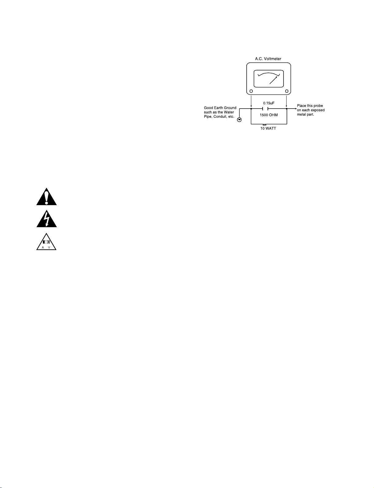
6. After reassembly of the set, always perform an AC leakage test on all exposed
metallic parts of the cabinet (the channel selector knobs, antenna terminals, handle
and screws) to be sure that set is safe to operate without danger of electrical shock.
DO NOT USE ALINE ISOLATION TRANSFORMER DURING THIS TEST. Use an
AC voltmeter having 5000 ohms per volt or more sensitivity in the following manner:
Connect a 1500 ohm, 10 watt resistor, paralleled by a .15 mfd 150V AC type
capacitor between a known good earth ground water pipe, conduit, etc.) and the
exposed metallic parts, one at a time. Measure the AC voltage across the
combination of 1500 ohm resistor and .15 mfd capacitor. Reverse the AC plug by
using a non-polarized adaptor and repeat AC voltage measurements for each
exposed metallic part. Voltage measured must not exceed 0.75 volts RMS. This
corresponds to 0.5 milliamp AC. Any value exceeding this limit constitutes a potential
shock hazard and must be corrected immediately.
TIPS ON PROPER INSTALLATION
1. Never install any receiver in a closed-in recess, cubbyhole, or closely fitting shelf
space over, or close to, a heat duct, or in the path of heated air flow.
2. Avoid conditions of high humidity such as: outdoor patio installations where dew is a
factor, near steam radiators where steam leakage is a factor, etc.
3. Avoid placement where draperies may obstruct venting. The customer should also
avoid the use of decorative scarves or other coverings that might obstruct ventilation.
4. Wall- and shelf-mounted installations using a commercial mounting kit must follow
the factory-approved mounting instructions. A product mounted to a shelf or platform
must retain its original feet (or the equivalent thickness in spacers) to provide
adequate air flow across the bottom. Bolts or screws used for fasteners must not
touch any parts or wiring. Perform leakage tests on customized installations.
5. Caution customers against mounting a product on a sloping shelf or in a tilted
position, unless the receiver is properly secured.
6. A product on a roll-about cart should be stable in its mounting to the cart.
Caution the customer on the hazards of trying to roll a cart with small casters across
thresholds or deep pile carpets.
7. Caution customers against using extension cords. Explain that a forest of
extensions, sprouting from a single outlet, can lead to disastrous consequences to
home and family.
Copyright © 2008 LG Electronics. Inc. All right reserved.
Only for training and service purposes
1-3
LGE Internal Use Only

SERVICING PRECAUTIONS
CAUTION: Before servicing the PORTABLE DVD covered by
this service data and its supplements and addends, read and
follow the SAFETY PRECAUTIONS. NOTE: if unforeseen
circumstances create conflict between the following servicing
precautions and any of the safety precautions in this
publication, always follow the safety precautions.
Remember Safety First :
General Servicing Precautions
1. Always unplug the PORTABLE DVD AC power cord from
the AC power source before:
(1) Removing or reinstalling any component, circuit board,
module, or any other assembly.
(2) Disconnecting or reconnecting any internal electrical
plug or other electrical connection.
(3) Connecting a test substitute in parallel with an
electrolytic capacitor.
Caution: A wrong part substitution or incorrect polarity
installation of electrolytic capacitors may result in an
explosion hazard.
2. Do not spray chemicals on or near this PORTABLE DVD or
any of its assemblies.
3. Unless specified otherwise in this service data, clean
electrical contacts by applying an appropriate contact
cleaning solution to the contacts with a pipe cleaner, cottontipped swab, or comparable soft applicator.
Unless specified otherwise in this service data, lubrication of
contacts is not required.
4. Do not defeat any plug/socket B+ voltage interlocks with
which instruments covered by this service manual might be
equipped.
5. Do not apply AC power to this PORTABLE DVD and / or any
of its electrical assemblies unless all solid state device heat
sinks are correctly installed.
6. Always connect the test instrument ground lead to an
appropriate ground before connecting the test instrument
positive lead. Always remove the test instrument ground
lead last.
Insulation Checking Procedure
Disconnect the attachment plug from the AC outlet and turn
the power on. Connect an insulation resistance meter (500V)
to the blades of the attachment plug. The insulation resistance
between each blade of the attachment plug and accessible
conductive parts (Note 1) should be more than 1Mohm.
Note 1: Accessible Conductive Parts include Metal panels,
Input terminals, Earphone jacks,etc.
Electrostatically Sensitive (ES) Devices
Some semiconductor (solid state) devices can be damaged
easily by static electricity. Such components commonly are
called Electrostatically Sensitive (ES) Devices. Examples of
typical ES devices are integrated circuits and some field effect
transistors and semiconductor chip components.
The following techniques should be used to help reduce the
incidence of component damage caused by static electricity.
1. Immediately before handling any semiconductor component
or semiconductor-equipped assembly, drain off any
electrostatic charge on your body by touching a known earth
ground. Alternatively, obtain and wear a commercially
available discharging wrist strap device, which should be
removed for potential shock reasons prior to applying power
to the unit under test.
2. After removing an electrical assembly equipped with ES
devices, place the assembly on a conductive surface such
as aluminum foil, to prevent electrostatic charge buildup or
exposure of the assembly.
3. Use only a grounded-tip soldering iron to solder or unsolder
ES devices.
4. Use only an anti-static solder removal device. Some solder
removal devices not classified as “anti-static” can generate
electrical charges sufficient to damage ES devices.
5. Do not use freon-propelled chemicals. These can generate
an electrical charge sufficient to damage ES devices.
6. Do not remove a replacement ES device from its protective
package until immediately before you are ready to install it.
(Most replacement ES devices are packaged with leads
electrically shorted together by conductive foam, aluminum
foil, or comparable conductive material).
7. Immediately before removing the protective material from
the leads of a replacement ES device, touch the protective
material to the chassis or circuit assembly into which the
device will be installed.
Caution: Be sure no power is applied to the chassis or
circuit, and observe all other safety precautions.
8. Minimize bodily motions when handling unpackaged
replacement ES devices. (Normally harmless motion such
as the brushing together of your clothes fabric or the lifting
of your foot from a carpeted floor can generate static
electricity sufficient to damage an ES device.)
LGE Internal Use Only
1-4
Copyright © 2008 LG Electronics. Inc. All right reserved.
Only for training and service purposes
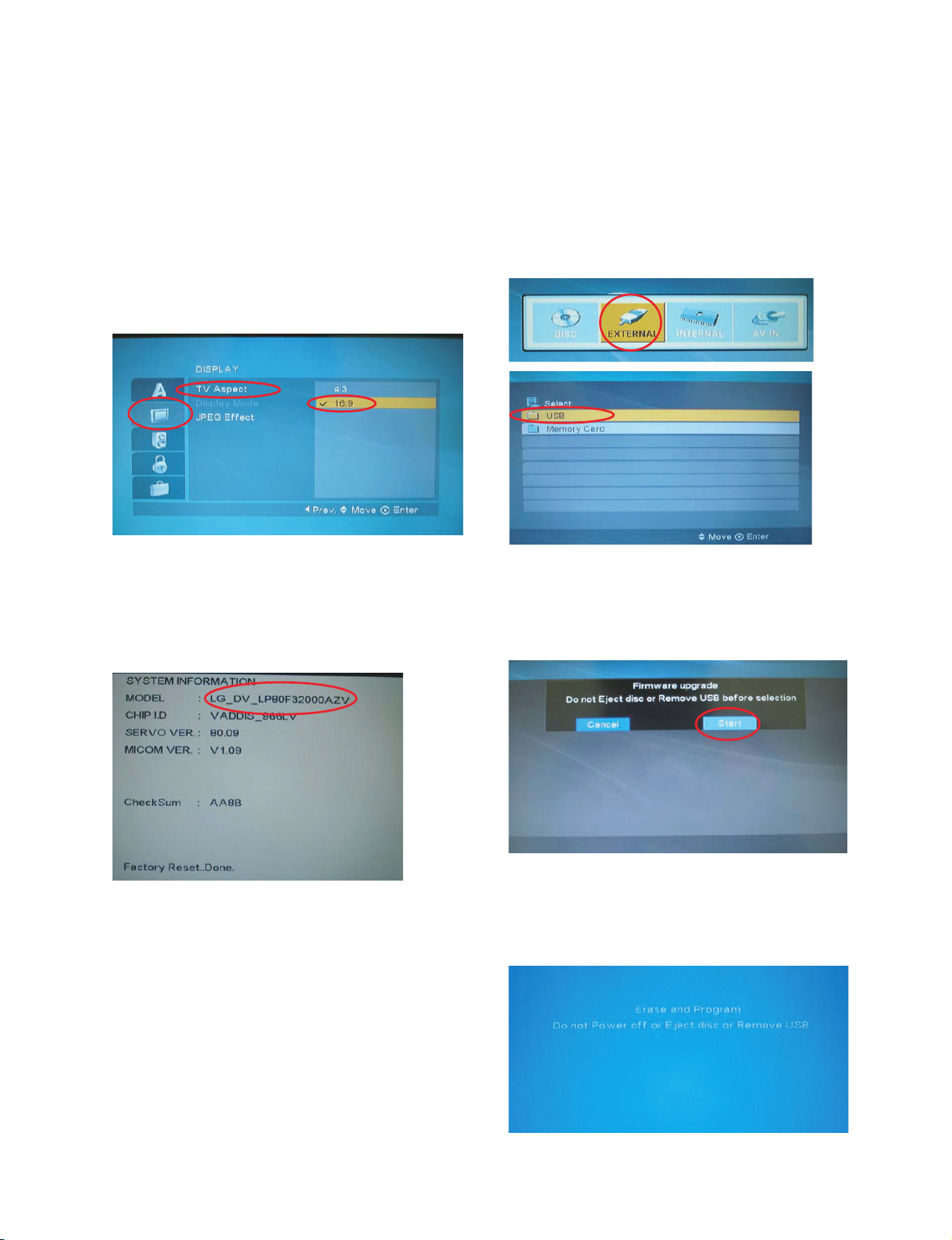
UPGRADING FIRMWARE
Please follow the below process to download a program with disc
1. Turn on the DVD-player.
(Note. Be sure that there is no disc in DVD-player)
2. Press “SETUP” button on Remote control.
3. Choose a “display” menu by using the cursor button
and then choose a “TV Aspect” menu. And choose
“16:9” menu.
4. Press the 1 --> 3 --> 9 --> 7 --> 1 --> 3 -->
9(numerical button) --> Enter key on remote control
to confirm the system information.
5. Remember or write the model name.
8. Insert the copied USB memory stick to DVD-player.
9. Press the MODE button on the Potable DVD-player.
10. Select External and USB.
11. If the below picture appears on the screen, Select
“Start” and Press “OK” button on Remote controller.
While this menu appears, please don’t eject
disc or take out USB
6. Change the program file name of new version to
the model name
Ex> New ver. program file -->
LG_DV_LP81F32000AZV_V014.ROM
Model name --> LG_DV_LV80F32000AZV
Change New ver. program file like this -->
LG_DV_ LV80F32000AZV.ROM
If you don”t change the file name like that, Disc
download isn”t be worked.
7. Copy the changed file to a USB memory stick.
Copyright © 2008 LG Electronics. Inc. All right reserved.
Only for training and service purposes
12.After the below picture appears on the screen, New
DVD program will download from USB memory
stick automatically.
Do not take out the USB memory stick.
1-5
LGE Internal Use Only
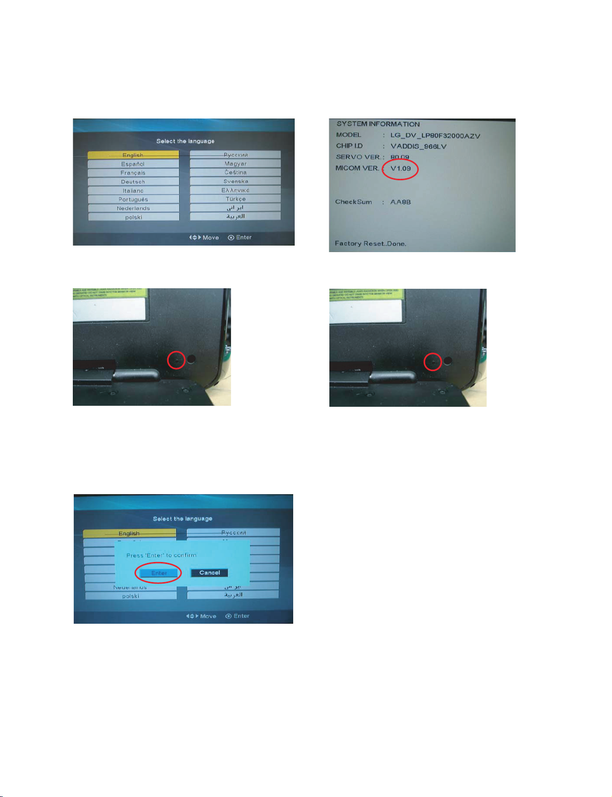
13.After USB download is completed, DVD-player
displays below picture automatically.
17.Do it again the process 1, 2, 3, 4 to confirm the
version.
14.Press the Reset button on the DVD-Player.
15.Remove the USB memory stick.
16.Turn on the DVD-player. Select the initial Language
and Press “Enter” button.
Then, Select “Enter” and Press “Enter” button.
18.Press the Reset button on the DVD-Player.
LGE Internal Use Only
1-6
Copyright © 2008 LG Electronics. Inc. All right reserved.
Only for training and service purposes

SPECIFICATIONS
• DVD PLAYER
Power supply DC 12V (AC adapter terminal), DC 7.5V (Battery)
Power consumption 12W
Weight 980g (without battery pack)
External dimensions(W X D X H) 230 X 145.5 X 39(mm)
Signal system PAL
Laser Semiconductor laser and 1 beam / 2LD System
Frequency range (audio) DVD linear sound:48kHZ sampling 4HZ to 20kHZ
Signal-to-noise ratio(audio) More than 80dB
Dynamic range(audio) More than 80dB
Harmonic distortion(audio) 0.04%
Operating conditions(audio) Temperature: 41°F to 95°F
• TERMINALS
DC input 1
Composite Video IN/OUTPUT 1
Audio IN/OUTPUT
Earphone output 2
Mini USB input 1
3 in 1 memory slot 1
• LIQUID CRYSTAL DISPLAY
Panel size 8inches (16:9)
Projection system TN color transmission
Driving system TFT active matrix
• SUPPLIED ACCESSORIES
RCA Audio/Video cable 1
AC Adapter (MPA-630A) 1
Car Adapter (WLD-041) 1
USB Cable 1
Remote control 1
Battery for Remote control (Lithium) 1
Copyright © 2008 LG Electronics. Inc. All right reserved.
Only for training and service purposes
1-7
LGE Internal Use Only

MEMO
LGE Internal Use Only
1-8
Copyright © 2008 LG Electronics. Inc. All right reserved.
Only for training and service purposes

SECTION 2
EXPLODED VIEWS
CONTENTS
EXPLODED VIEWS .....................................................................................................................................2-2
1. CABINET AND MAIN FRAME SECTION ..................................................................................................2-2
2. PACKING ACCESSORY SECTION...........................................................................................................2-3
Copyright © 2008 LG Electronics. Inc. All right reserved.
Only for training and service purposes
2-1
LGE Internal Use Only
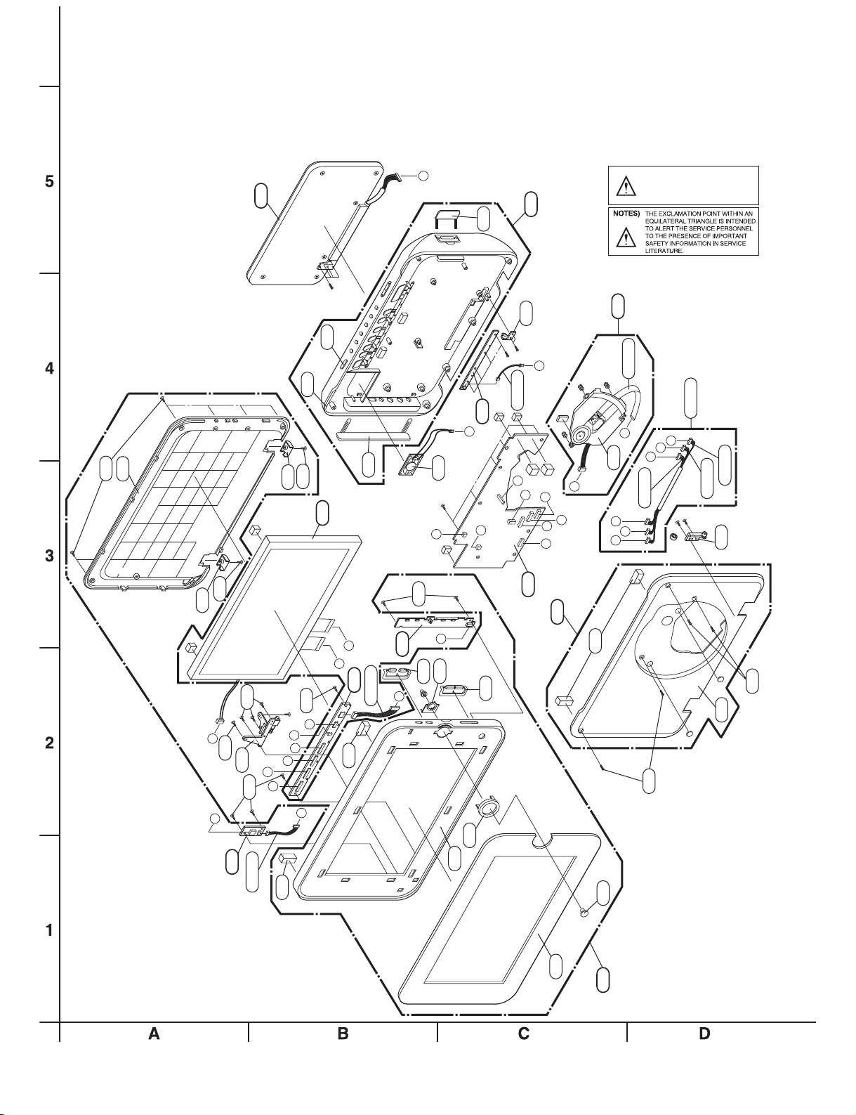
EXPLODED VIEWS
1. CABINET AND MAIN FRAME SECTION
271
272
A47
270
O
79
2
CABLE8
I
H
A44
N
H
J
K
L
O
264
262
260
A50
M
271
263
A40
277
M
N
CAUTION)
Do not reuse the battery cell,
after separating the battery
cell from the battery case.
00
A
CABLE5
I
278
G
F
E
K
J
ABLE4
C
L
CABLE1
CABLE2
CABLE3
276
71
2
270
D
C
A51
257
ABLE7
C
258
B
258
259
6
25
B
A52
CABLE6
6
25
G
P
F
D
C
E
P
257
A
A53
6
25
A
4
25
255
255
252
253
A46
A48
0
25
74
2
75
2
73
2
275
251
A43
LGE Internal Use Only
2-2
Copyright © 2008 LG Electronics. Inc. All right reserved.
Only for training and service purposes
2. PACKING ACCESSORY SECTION
834
CABLE, CIGAR JACK
836
CABLE, USB
806
PLUG ASS'Y(RCA CABLE)
833
CORD
900
REMOTE CONTROL
808
801
OWNER'S MANUAL
804
PACKING SHEET
BATTERY
803
BAG
802A
BOX
802
BOX
Copyright © 2008 LG Electronics. Inc. All right reserved.
Only for training and service purposes
2-3
802B
BOX
LGE Internal Use Only

MEMO
LGE Internal Use Only
2-4
Copyright © 2008 LG Electronics. Inc. All right reserved.
Only for training and service purposes

SECTION 3
ELECTRICAL
CONTENTS
LCD PART........................................................3-2
LCD ELECTRICAL
TROUBLESHOOTING GUIDE ....................3-2
WIRING CONNECTION DIAGRAM...........3-3
LCD PCB <---> KEY PCB, BACK LIGHT,
LCD PANNEL.....................................................3-3
INTERFACE DIAGRAM.................................3-4
LCD PCB <---> KEY PCB INTERFACE.............3-4
BLOCK DIAGRAM ..........................................3-5
CIRCUIT DIAGRAMS .....................................3-7
1. LCD I/F CIRCUIT DIAGRAM .........................3-7
2. PANEL I/F CIRCUIT DIAGRAM.....................3-9
3. FRONT KEY BOARD
CIRCUIT DIAGRAM .....................................3-11
4. LCD BACKLIGHT CIRCUIT DIAGRAM.......3-13
PRINTED CIRCUIT BOARD
DIAGRAMS......................................................3-15
1. LCD P.C.BOARD..........................................3-15
2. FRONT KEY P.C.BOARD ............................3-15
3. BACK-LIGHT P.C.BOARD ...........................3-16
7. LCD DRIVE IC(U701) SYSTEM CLOCK
(27MHz)........................................................3-32
8. ZR36966 VIDEO OUTPUT WAVEFORM ....3-32
9. AUDIO OUTPUT FROM AUDIO DAC .........3-33
WIRING CONNECTION DIAGRAMS ......3-34
1. OVERALL CONNECTION LAYOUT
DIAGRAM.....................................................3-34
2. WIRING CONNECTION DIAGRAM-1 .........3-35
3. WIRING CONNECTION DIAGRAM-2 .........3-36
INTERNAL BLOCK DIAGRAM OF ICs..3-37
1. MOTOR DRIVE IC(AM5898N).....................3-37
2. LCD DRIVE IC(T103)...................................3-39
3. VOLUME CONTROLLER IC(PT2257).........3-43
4. SPEAKER AMP IC(PT2303)........................3-44
5. MICOM IC(GT6319).....................................3-45
INTERFACE DIAGRAM...............................3-47
MAIN <---> LCD PCB INTERFACE .................3-47
BLOCK DIAGRAMS .....................................3-48
1. OVERALL BLOCK DIAGRAM......................3-48
2. POWER BLOCK DIAGRAM ........................3-49
3. MPEG BLOCK DIAGRAM ...........................3-50
4. DISC BLOCK DIAGRAM .............................3-51
5. AV BLOCK DIAGRAM..................................3-52
MAIN PART....................................................3-19
MAIN ELECTRICAL
TROUBLESHOOTING GUIDE ..................3-19
1. POWER (DC-DC CONVERTER)
CIRCUIT.......................................................3-19
2. MPEG CIRCUIT...........................................3-22
3. RF/SERVO CIRCUIT ...................................3-23
4. CHARGEING CIRCUIT................................3-26
DETAILS AND WAVEFORMS ON
SYSTEM TEST AND DEBUGGING.........3-27
1. SYSTEM 27MHz CLOCK ............................3-27
2. SDRAM CLOCK...........................................3-27
3. DISC TYPE JUDGEMENT WAVEFORM.....3-28
4. FOCUS ON WAVEFORM ............................3-30
5. SPINDLE CONTROL WAVEFORM
(NO DISC CONDITION)...............................3-30
6. TRACKING CONTROL RELATED SIGNAL
(SYSTEM CHECKING) ................................3-31
Copyright © 2008 LG Electronics. Inc. All right reserved.
Only for training and service purposes
CIRCUIT DIAGRAMS ...................................3-53
1. MPEG CIRCUIT DIAGRAM .........................3-53
2. MEMORY CIRCUIT DIAGRAM....................3-55
3. OPU & MOTOR CIRCUIT DIAGRAM..........3-57
4. AV CIRCUIT DIAGRAM ...............................3-59
5. CHARGE CIRCUIT DIAGRAM ....................3-61
6. MAIN KEY CIRCUIT DIAGRAM ..................3-63
CIRCUIT VOLTAGE CHART......................3-65
1. IC VOLTAGE CHART...................................3-65
2. CAPACITOR VOLTAGE CHART..................3-66
PRINTED CIRCUIT
BOARD DIAGRAMS.....................................3-67
1. MAIN P.C.BOARD ........................................3-67
2. MAIN KEY P.C.BOARD................................3-67
3. MIS P.C.BOARD ..........................................3-69
3-1
LGE Internal Use Only
LCD PART
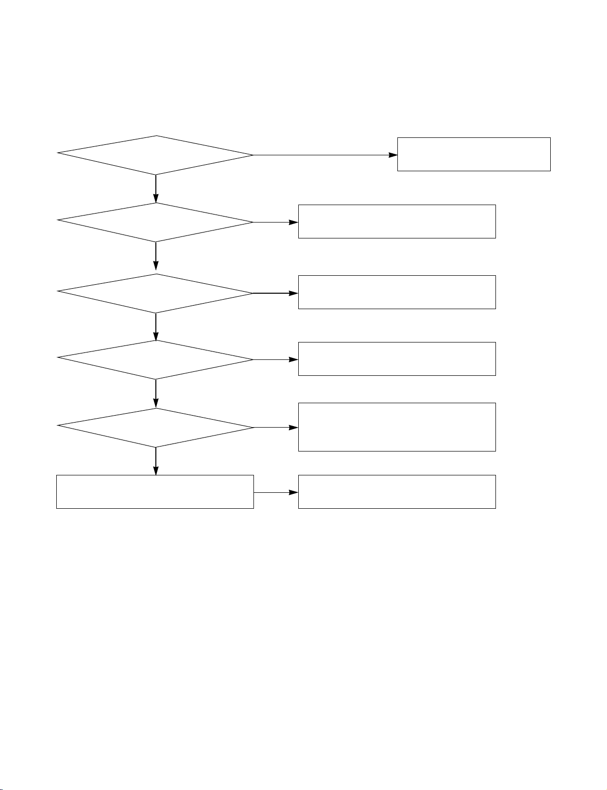
LCD ELECTRICAL TROUBLESHOOTING GUIDE
Appear shadow form
Display condition?
YES
interference in black background
NO
Inverter abnormal
Backlight condition?
YES
+10V, 15V, -10V normal?
YES
+10V normal?
YES
RGB signal output?
YES
NO
NO
NO
NO
NO
U704, Q701, Q702 check
FB701, FB702, L703, U703 check
L801, L802, FB701, FB702
Check LCD driver IC(U701)
R : 58, 59, 62, 63, 64, 65
G : 49, 50, 52, 53, 54, 55
B : 38, 40, 42, 43, 44, 45
Check L802VOCM level(3.3V)?
LGE Internal Use Only
3-2
Copyright © 2008 LG Electronics. Inc. All right reserved.
Only for training and service purposes
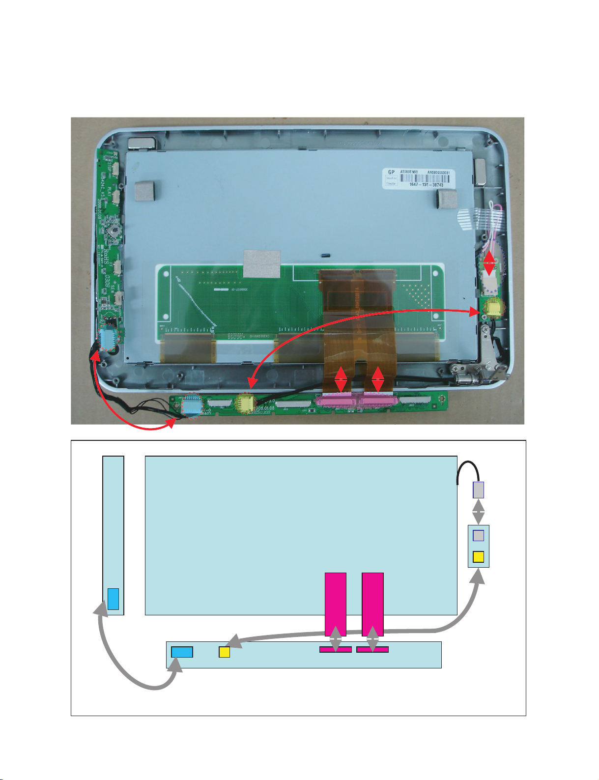
WIRING CONNECTION DIAGRAM
LCD PCB <---> KEY PCB, BACK LIGHT, LCD PANNEL
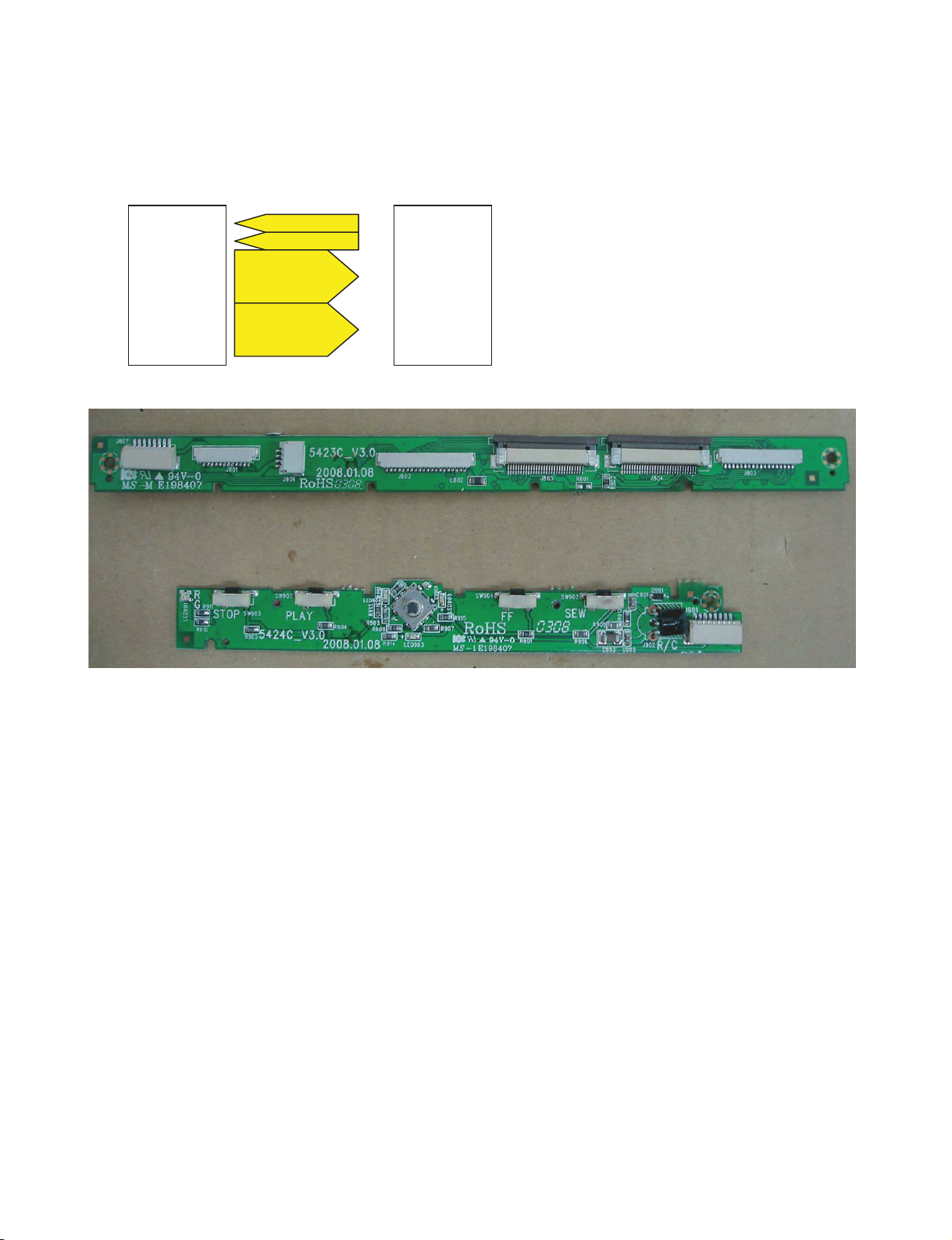
Front key PCB
Copyright © 2008 LG Electronics. Inc. All right reserved.
Only for training and service purposes
LCD Pannel
LCD PCB
3-3
Back-light PCB
LGE Internal Use Only
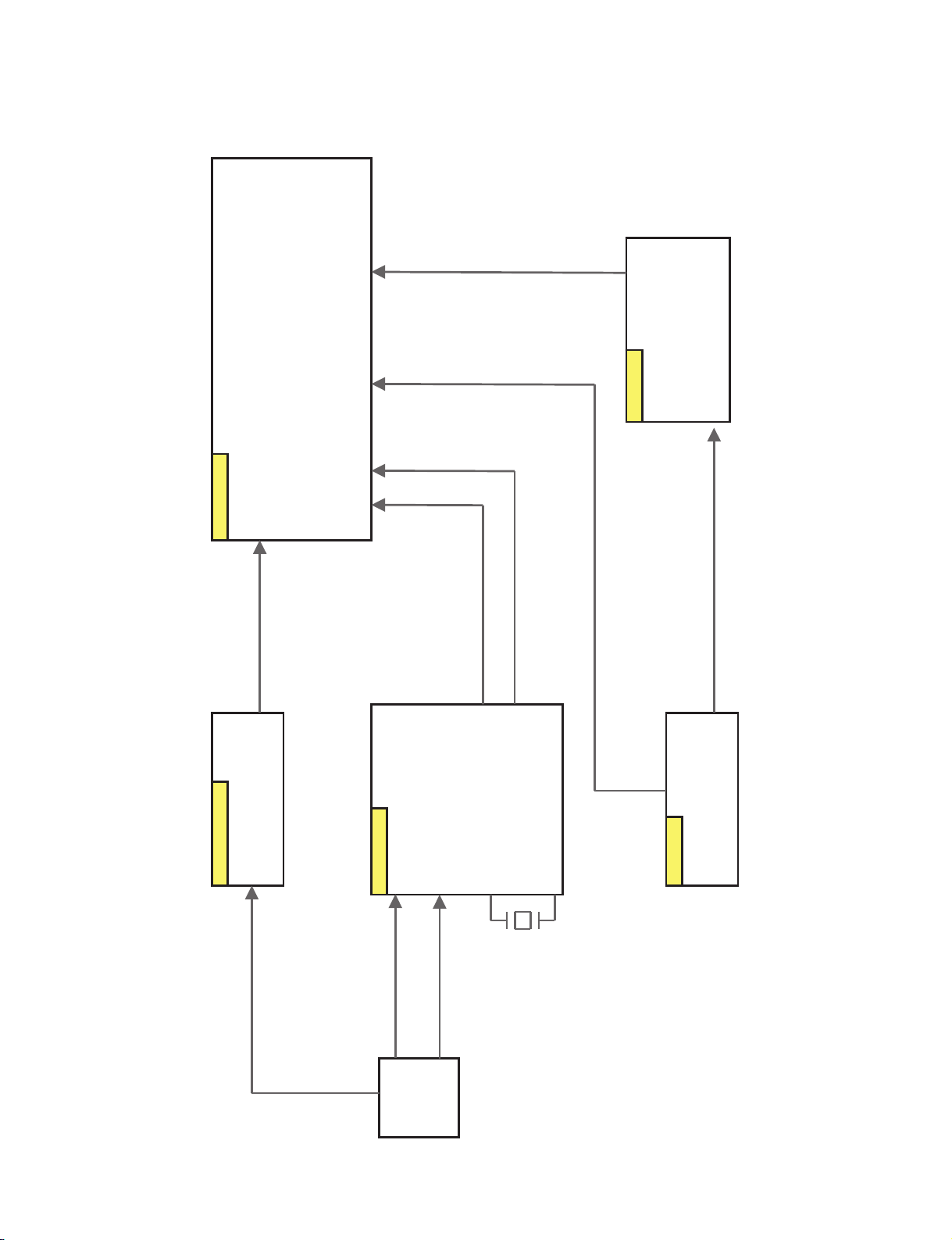
INTERFACE DIAGRAM
8
8 1
807
901
LCD PCB <---> KEY PCB INTERFACE
1
2
3
4
5
6
7
8
K2
IR
LED_G
LED_R
LED_B
GND
5VA
GND
1
J807
8
KEY data
R/C d ata
LED Control
Power
J901
K2
8
IR
7
LED_G
6
LED_R
5
LED_B
4
GND
3
5VA
2
GND
1
81
LGE Internal Use Only
3-4
Copyright © 2008 LG Electronics. Inc. All right reserved.
Only for training and service purposes
BLOCK DIAGRAM
INNOLUX
V1~V14
TABLE
8î inch
LCD PANEL
3.3V
GAMMA
10V
BAT_OUT
LED_POWER
LCD
Backlight
PWRCTL_LCD
INVERTER
2.5V/3.3V
VID[0] ~ VID[7]
VCLK, SCL,
POL,STHR,STHL,DCLK
LP,GCLK,GOE,STVL,
STVR,R/L,U/P,EDGSL
T103
SDA, STB
VGH , VGL
R(0~5),G(0~5),B(0~5)
LCD Drive
Terawins
27MHz
VLC (10V)
BLOCK
LCD_POWER
3.3V
Copyright © 2008 LG Electronics. Inc. All right reserved.
Only for training and service purposes
MPEG
ZORAN
3-5
ZORAN966_LV
LGE Internal Use Only

MEMO
LGE Internal Use Only
3-6
Copyright © 2008 LG Electronics. Inc. All right reserved.
Only for training and service purposes
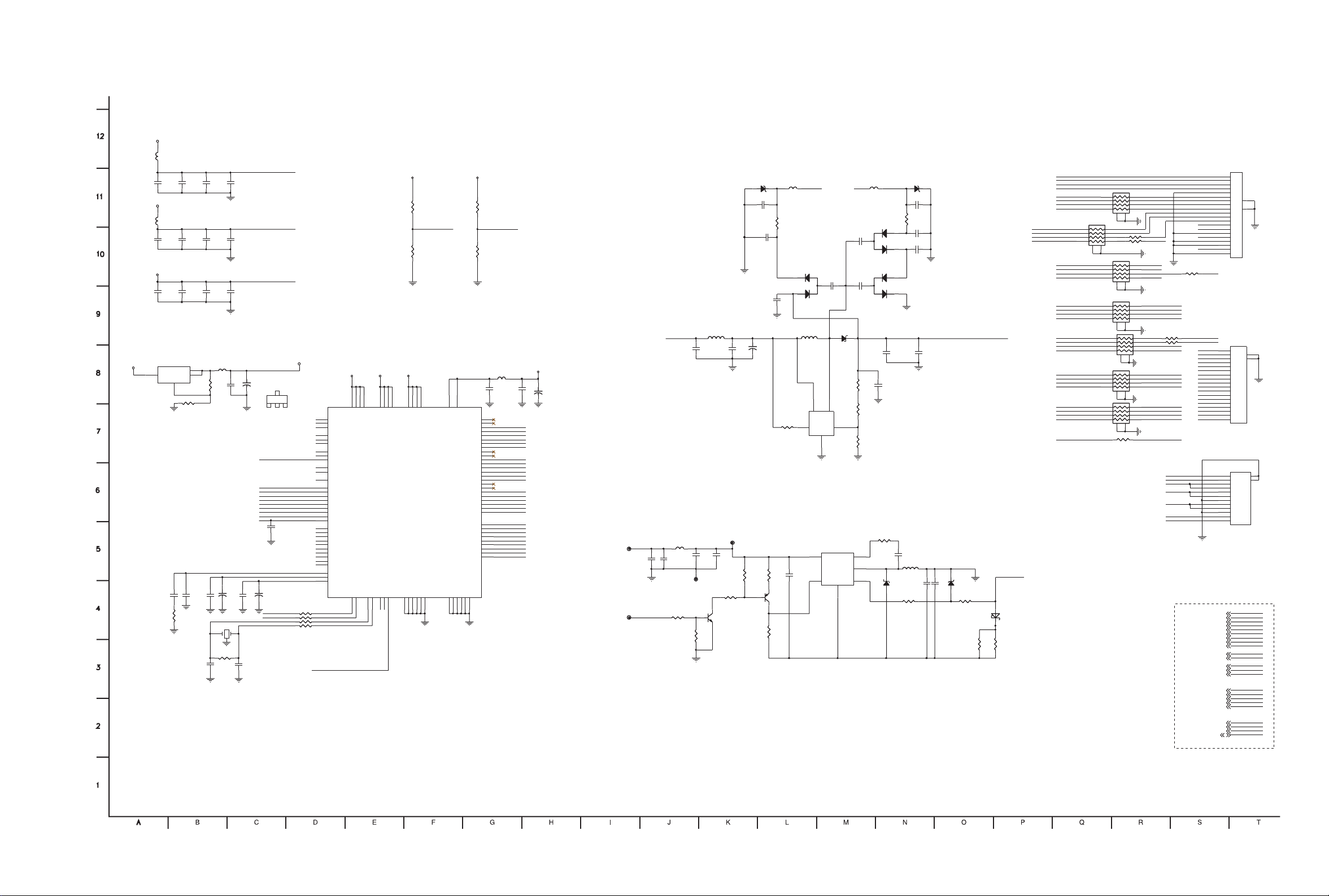
07.LCD I/F07.LCD I/F07.LCD I/F
Friday, February 15, 2008Friday, February 15, 2008Friday, February 15, 2008
CKVD
POL
OEV
D
STVL
D
POL
D
G
0
B
3
B
4
B
5
VCL
K
AVDD3
3
K
2
I2C_SC
L
VID
1
I2C_SD
A
I2C_SC
L
I
R
G
5
R
5
R
4
R
2
R
3
R1
R
0
G
4
G
3
G
2
G
1
/M_RESE
T
G
0
B
5
B
4
B
3
B
2
B
1
B
0
PO
L
STH
R
STH
L
CL
K
VID
2
OE
H
CK
V
OE
V
STV
R
STV
L
VDD2
5
LED_
G
VDD3
3 R/LU/D
VID
3
I2C_SD
A
LED_
R
VID
4
PWRCTL_LC
D
VID
5
BAT_OU
T
VID
6
3.3
V
VID
0
5V
A
VID
7
STHL
D
STHR
D
B4
D
B3
D
R/
L
B
2
B
0
B
1
G1
D
G2
D
G3
D
STVR
D
G4
D
R1
D
R2
D
R3
D
R4
D
U/
D
STH
R
G
4
G
1
G
2
G
3
OE
H
CL
K
STV
R
STV
L
OE
V
R
0
R
1
STH
L
G
5
CK
V
R
5
R
2
R
4
R
3
OEH
D
R5
D
U/D
D
VID
5
VID
7
VID
4
VID
6
VID
3
VID
2
VID
1
VID
0
CVBS_IN_LC
D
CVBS_IN_LC
D
/M_RESE
T
GN
D
K
2
I
R
LED_
G
LED_
R
B0
D
B1
D
B2
D
G3
D
G2
D
G1
D
G0
D
STVR
D
STVL
D
OEV
D
CKV
D
OEH
D
CLK
D
STHL
D
STHR
D
POL
D
U/D
D
R5
D
R4
D
R3
D
R2
D
R1
D
R0
D
G5
D
G4
D
BAT_OU
T
PWRCTL_LC
D
3.3
V VLC
VG
HVGL
LED_POWE
R
VG
H
VG
L
LED_
B
5V
A
3.3
V
LED_POWE
R
VL
C
LED_
B
VCL
K
CLK
D
G5
D
R0
D
B5
D
G0
D
VDD3
3VDD33
AVDD3
3VDD25VDD33
AVDD3
3
3.3
V
2.5
V
3.3
V
3.3
V
2.5
V
VCLK
2
K2
6
I2C_SCL2,
5
VID1
2
IR
6
/M_RESET2,3,
6
VID2
2
LED_G
6
VID3
2
I2C_SDA2,
5
LED_R
6
VID4
2
PWRCTL_LCD
2
VID5
2
BAT_OUT4,
6
VID6
2
VID0
2
3.3V2,3,
4
5VA4, 5,
6
VID7
2
CVBS_IN_LCD
2
LED_B
6
GND2,3,4, 5,6
AZ1117H-ADJ SMD
31
4
2
VGH=+15V VGL=-10V
VLC=+10V
OFF-PAGE CONNECTION
<AVDD33>
P.ON(3.25V/30mA)
DVD_PLAY(3.24V/30mA)
<VDD33>
P.ON(3.25V/40mA)
DVD_PLAY(3.25V/40mA)
<2.5V>
P.ON(2.35V/90mA)
DVD_PLAY(2.35V/92mA)
<VLC>
P.ON(3.25V/140mA)
DVD_PLAY(3.24V/155mA)
<Backlight>
P.ON(7.48V/140mA)
DVD_PLAY(7.48V/140mA)
Changed component :
RN701~RN707 7EA(33ohm array resistant --> MEA3216L50R0T Array bead
)
C735
22uF/16
V
C735
22uF/16V
R727
6.8 1
%
R727
6.8 1%
1 2
D706
SS1
4
D706
SS14
C707
0.1u
F
C707
0.1uF
L703
10u
H
L703
10uH
R721
68
K
R721
68K
C701
0.1u
F
C701
0.1uF
L705
LSS57S30-33
0
L705
LSS57S30-330
R718
2
K
R718
2K
C706
0.1u
F
C706
0.1uF
TP70
2TP702
C713
0.1u
F
C713
0.1uF
R714
6.2
K
R714
6.2K
12
+
CM703
100uF/10
V
+
CM703
100uF/10
V
R728
N
C
R728
NC
R719
10
K
R719
10K
R734 3
3R734 33
C714
0.1u
F
C714
0.1uF
TP70
4TP704
R717
10
K
R717
10K
R715
7.5
K
R715
7.5K
C737
2.2uF/25V X5
R
C737
2.2uF/25V X5R
2 3
1
B
C
E
Q702
2N390
6
B
C
E
Q702
2N390
6
R708
1
M
R708
1M
C741
10uF/25
V
C741
10uF/25V
C731
0.1u
F
C731
0.1uF
C728
0.1u
F
C728
0.1uF
3
2
1
D705
BAT54S
D705
BAT54S
ACB2
2
ACB1
3
ACB0
4
HSI
1
9
AGNDB
5
AGNDG
1
0
AGNDR
1
5
AY2
7
AY1
8
AY0
9
ACR2
1
2
ACR1
1
3
ACR0
1
4
VSI
1
8
SOYIN
9
7
AVDDP
9
1
AVDDP
9
5
QE0
3
6
QE1
3
7
QE2
3
8
QE3
4
0
QE4
4
2
QE5/sRL
4
3
QE6/sUD
4
4
QE7/sHSo
4
5
QE8/sVSo
4
6
QE9/sDEN
4
7
QE10/sD0
4
9
QE11/sD1
5
0
QE12/sD2
5
2
QE13/sD3
5
3
QE14/sD4
5
4
QE15/sD5
5
5
QE16/sD6
5
6
QE17/sD7
5
7
QE18/VDT10/CC_B
5
8
QE19/VDT11/CC_G
5
9
QE20/VDT12/CC_R
6
2
QE21/VDT13/CC_BOX
6
3
QE22/VDT14/CC_Y
6
4
QE23/VDT15/CC_CKO
6
5
HSO/PO L
6
7
VSO/STH1
6
8
DEN/ST H2
6
9
CLKO/CLKH
7
1
LP
7
2
GCLK
7
4
GOE
7
5
STV1
7
6
STV2
7
7
VDT0
7
8
VDT1
7
9
VDT2
8
0
VDT3
8
1
VDT4
8
2
VDT5
8
3
VDT6
8
4
VDT7
8
5
VCLK
8
6
SDA
2
1
SCL/SCAN B
2
2
XTALI
2
4
XTALO
2
5
FILT
9
3
VPLL
9
4
VREF
9
8
PWM3/VDT8/CC_HSO
3
0
GPIO3/VDT9/CC_VSO
3
4
GPIO2/VDT17/VDT10/CC_B/AP
3
3
GPIO1/VDT11/CC_G/Q1H
3
2
GPIO0/VDT12/CC_R
3
1
PWM2/VDT16/VDT13 /CC_BOX
2
9
PWM1/VDT14/CCY
2
8
IR1/VDT15/CC_CKO
2
7
LODD/LVSync
8
7
LHREF/LHSnC
8
8
XCLK2MC
2
6
RSTB
2
0
CPUINT
2
3
AVDDB
1
AVDDG6AVDDR
1
1
AVDDDAC
9
9
VDD25
1
7
VDD25
4
1
VDD25
6
6
VDD25
8
9
VDD33
3
5
VDD33
4
8
VDD33
6
1
VDD33
7
3
GNDP
9
2
GNDP
9
6
GNDAC
10
0
GND
1
6
GND
3
9
GND
5
1
GND
6
0
GND
7
0
GND
9
0
U701
T10
3
U701
T103
R731
0
R731
0
12
+
CM704
100uF/10
V
+
CM704
100uF/10V
12
+
C733
22uF/16
V
+
C733
22uF/16
V
C702
0.1u
F
C702
0.1uF
C729
0.1u
F
C729
0.1uF
R725
10
K
R725
10K
C708
0.1u
F
C708
0.1uF
R723
10
K
R723
10K
C721
0.1u
F
C721
0.1uF
TP70
3TP703
C704
0.1u
F
C704
0.1uF
C740
0.33u
F
C740
0.33uF
R711
68
0
R711
680
1
82
73
64
9
510
RN702
MEA3216L101
R
RN702
MEA3216L101R
1
82
73
64
9
510
RN707
MEA3216L101
R
RN707
MEA3216L101R
C711
0.1u
F
C711
0.1uF
1
82
73
64
9
510
RN705
MEA3216L101
R
RN705
MEA3216L101R
R704 3
3R704 33
R701
0
R701
0
C730
0.1u
F
C730
0.1uF
12
+
CM702
100uF/10
V
+
CM702
100uF/10
V
C746
20p
F
C746
20pF
C703
0.1u
F
C703
0.1uF
C743
0.1u
F
C743
0.1uF
1 2
L701
FB060
3
L701
FB0603
R732 3
3R732 33
R729
270
K
R729
270K
10
9
8
7
6
5
4
3
2
1
1
1
1
3
1
2
1
5
1
4
1
6
2
0
1
9
1
8
1
7
2
1
2
2
J702
CON20_0.8M
M
J702
CON20_0.8MM
R712 68
0R712 680
R733 3
3R733 33
1 2
FB702
FB080
5
FB702
FB0805
1 2
D707
SS1
4
D707
SS14
R722
1
K
R722
1K
C742
0.01u
F
C742
0.01uF
1 2
L707
FB060
3
L707
FB0603
C722
4.7uF/25
V
C722
4.7uF/25V
C736
22uF/16
V
C736
22uF/16V
C720
0.1u
F
C720
0.1uF
C734
0.1u
F
C734
0.1uF
C744
0.1u
F
C744
0.1uF
1
82
73
64
9
510
RN704
MEA3216L101
R
RN704
MEA3216L101R
1
1
2
2
3
3
4
4
5
5
6
6
7
7
8
8
16
1
6
15
1
5
9
9
10
1
0
11
1
1
12
1
2
13
1
3
14
1
4
17
1
7
18
1
8
19
1
9
20
2
0
J701
CON18_0.8M
M
J701
CON18_0.8MM
1 2
D704
D_10
V
D704
D_10V
C716
20p
F
C716
20pF
C726
1u
F
C726
1uF
R730 1
0R730 10
1
82
73
64
9
510
RN706
MEA3216L101
R
RN706
MEA3216L101R
1 2
D701
D_15
V
D701
D_15V
R735 3
3R735 33
C705
0.1u
F
C705
0.1uF
1
82
73
64
9
510
RN703
MEA3216L101
R
RN703
MEA3216L101R
3
2
1
D703
BAT54
S
D703
BAT54S
R724
10
K
R724
10K
R705 3
3R705 33
C739
2.2uF/16V X5
R
C739
2.2uF/16V X5R
C715
22p
F
C715
22pF
IN
5SW1
EN
4
GND
2
FB
3
U703
RCR256
1
U703
RCR2561
C738
10uF/25
V
C738
10uF/25V
R710
N
C
R710
NC
1 2
FB701
FB080
5
FB701
FB0805
R702
N
C
R702
NC
C732
0.1u
F
C732
0.1uF
R713 3
3R713 33
1 2
L708
FB060
3
L708
FB0603
C727
0.1u
F
C727
0.1uF
R707 75(1%
)R707 75(1%)
C725 1u
FC725 1uF
OUT
2
IN
3
GND
1
TAB
4
U702
AZ1117H-ADJ SM
D
U702
AZ1117H-ADJ SMD
L704
6.8u
H
L704
6.8uH
1
82
73
64
9
510
RN701
MEA3216L101
R
RN701
MEA3216L101R
1 2
L706
FB120
6
L706
FB1206
12
D709
B340L
A
D709
B340LA
1
1
2
2
3
3
4
4
5
5
6
6
7
7
8
8
9
9
10
1
0
11
1
1
12
1
2
13
13
14
1
4
J703
CON12_0.8M
M
J703
CON12_0.8MM
1
3 2
B
C
E
Q701
2N390
4
B
C
E
Q701
2N3904
C709
0.1u
F
C709
0.1uF
C723
4.7uF/25
V
C723
4.7uF/25V
TP70
1TP701
R716
68
K
R716
68K
IN
5
EN
4
GND
2
BST
1
FB
3
SW
6
U704
MP2359D
T
U704
MP2359DT
R726
10
K
R726
10K
C712
0.1u
F
C712
0.1uF
R709
15
K
R709
15K
1 2
L702
FB(1206)
L702
FB(1206)
1 2
3
X701
27MH
z
X701
27MHz
C710
0.1u
F
C710
0.1uF
C718
3300p
F
C718
3300pFC717
0.1u
F
C717
0.1uF
R706
0R706 0
C719
330p
F
C719
330pF
1 2
D708
13
V
D708
13V
3
2
1
D702
BAT54
S
D702
BAT54S
R720
100
K
R720
100K
R703
0
R703
0
12
+
CM701
100uF/10
V
+
CM701
100uF/10V
C724
1u
F
C724
1uF
CIRCUIT DIAGRAMS
1. LCD I/F CIRCUIT DIAGRAM
Copyright © 2008 LG Electronics. Inc. All right reserved.
Only for training and service purposes
3-7 3-8
LGE Internal Use Only
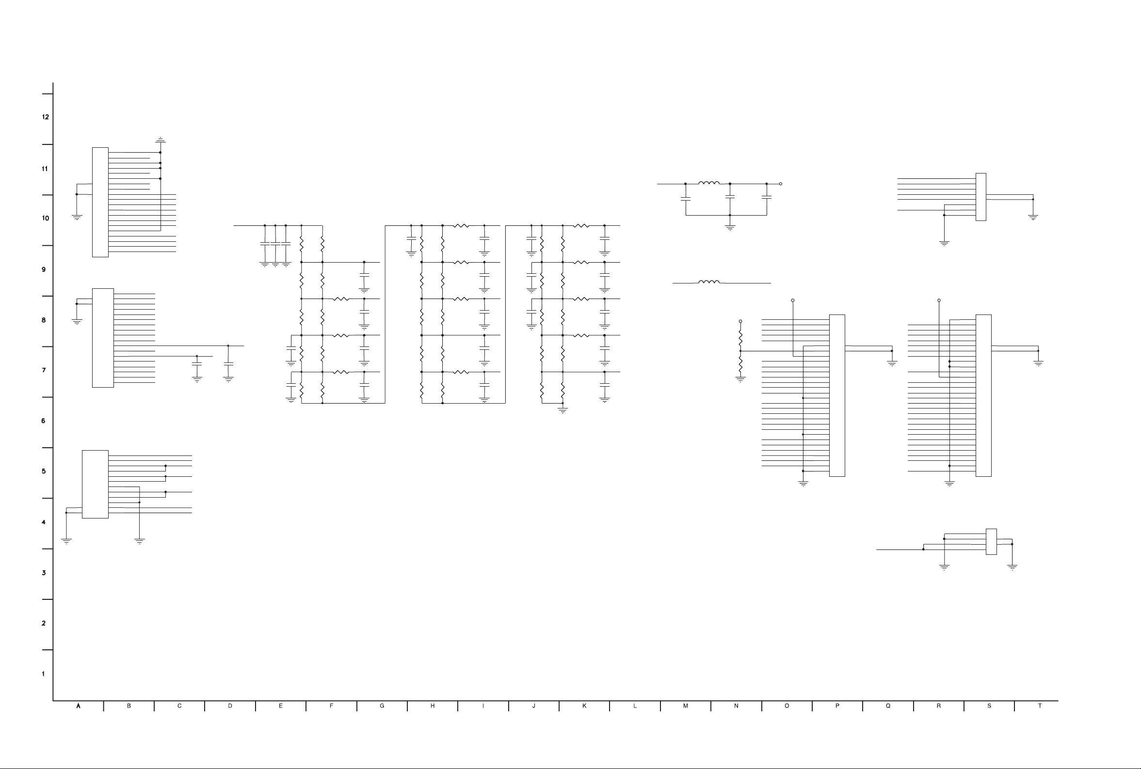
2. PANEL I/F CIRCUIT DIAGRAM
08.PANEL I/F08.PANEL I/F08.PANEL I/F
Friday, February 15, 2008Friday, February 15, 2008Friday, February 15, 2008
B3
G
5
B2
B
0
G
0
B
1
G
4
G
2
G
3
G
1
R/
L
STH
L
CL
K
B
5
STH
R
B
4
OE
H
POL
STV
R
OE
V
CK
V
STV
L
VL
C
VL
C
V1
2
V1
3
V
9
VG
L
V
2
VG
H
V
6
U/
D
VCO
M
VCO
M
V1
4
V1
1
V
8
V
5
V
3
R
4
R
3
R
0
V
1
V
4
V
7
V1
0
R
2
R
1
R
5
V1
3
V1
0
V1
1
VL
C
V
7
V
1V6
V
2
V
5
V1
2
V
3
V
9V14
V
8
V
4
K
2
I
R
LED_
G
LED_
R
3.3
VVCOM
STH
R
PO
L
U/
D
R
5
R
4
R
3
STV
R
R2
STV
L
R
1
OE
V
R
0
CK
V
G
5
OE
H
G
4
STH
L
G
0
LED_
R
R/
L
B
0
B
1
B
2
B
3
B
4
B
5
K
2
G
3
I
R
G
2
LED_
G
G
1
3.3
V
5V
A
3.3
V
LED_POWE
R
VL
C
VG
H
VG
L
5V
A
LED_
B
LED_
B
LED_POWE
R
CL
K
3V3
P3V3P
3V3
P
3V3
P
VCC=3.3V
AVDD=+10V
VGL=-10V
VGH=+15V
VCOM=3.3V
AVDD=+10V
VCOM=3.3V
VCC=3.3V
8.034V
7.419V
6.936V
6.157V
5.400V
4.600V
3.843V
3.064V
2.581V
1.966V
0.586V
10.0V
0.525V
9.475V
9.414
V
R817
8
2
R817
82
R814
1.5
K
R814
1.5K
C804
0.1u
F
C804
0.1uF
C806
0.1u
F
C806
0.1uF
R842
0
R842
0
R831
5
6
R831
56
R813
9
1
R813
91
R843
0
R843
0
R826
3
K
R826
3K
10
9
8
7
6
5
4
3
2
1
1
1
1
3
1
2
1
5
1
4
1
6
2
0
1
9
1
8
1
7
2
1
2
2
J80 2
CON20_0.8M
M
J80 2
CON20_0.8MM
C802
0.1u
F
C802
0.1uF
C818
22uF/16
V
C818
22uF/16V
R839
0
R839
0
R8350R835
0
R808
6.2
K
R808
6.2K
C828
20p
F
C828
20pF
R837
0
R837
0
R802
0
R802
0
R836
0
R836
0
R822
1.5
K
R822
1.5K
C822
2.2u
F
C822
2.2uF
1
2
3
4
5
6
7
8
9
1
0
J80 7
CON8_1.0M
M
J80 7
CON8_1.0MM
R811
5
6
R811
56
C821
2.2u
F
C821
2.2uF
C814
0.1u
F
C814
0.1uF
C825
2.2u
F
C825
2.2uF
R812
1
K
R812
1K
1
2
345
6
J806
CON4_1.0M
M
J806
CON4_1.0MM
R801
N
C
R801
NC
C803
0.1u
F
C803
0.1uF
1
1
2
2
3
3
4
4
5
5
6
6
7
7
8
8
9
9
10
1
0
11
1
1
12
1
2
13
13
14
1
4
J80 1
CON12_0.8M
M
J80 1
CON12_0.8MM
1
1
2
2
3
3
4
4
5
5
6
6
7
7
8
8
16
1
6
15
1
5
9
9
10
1
0
11
1
1
12
1
2
13
1
3
14
1
4
17
1
7
18
1
8
19
1
9
20
2
0
J80 3
CON18_0.8M
M
J80 3
CON18_0.8MM
C819 2.2uFC819 2.2uF
R827
15
0
R827
150
C805
0.1u
F
C805
0.1uF
R825
6
8
R825
68
R824
1
K
R824
1K
R841
0
R841
0
C816
0.1u
F
C816
0.1uF
R807
15
0
R807
150
C809
0.1u
F
C809
0.1uF
R804
1
K
R804
1K
R832
1
K
R832
1K
L802
F
B
L802
FB
C824
2.2u
F
C824
2.2uF
R810
3
K
R810
3K
R805
1
2
R805
12
R809
6
8
R809
68
R834
0
R834
0
10
9
8
7
6
5
4
3
2
1
1
1
1
3
1
2
1
5
1
4
1
6
2
0
1
9
1
8
1
7
3
0
2
9
2
8
2
7
2
6
2
5
2
4
2
3
2
2
2
1
3
1
3
2
J80 4
CON30_0.5M
M
J80 4
CON30_0.5MM
R818
3.3
K
R818
3.3K
C810
0.1u
F
C810
0.1uF
R820
1.5
K
R820
1.5K
C815
0.1u
F
C815
0.1uF
R806
1
5
R806
15
C807
0.1uF
C807
0.1uF
C813
0.1u
F
C813
0.1uF
C811
0.1u
F
C811
0.1uF
R82356R823
56
C812
0.1u
F
C812
0.1uF
R840
0
R840
0
L801
10u
H
L801
10uH
R838
0
R838
0
R828
6.2
K
R828
6.2K
C827
56p
F
C827
56pF
10
9
8
7
6
5
4
3
2
1
1
1
1
3
1
2
1
5
1
4
1
6
2
0
1
9
1
8
1
7
3
0
2
9
2
8
2
7
2
6
2
5
2
4
2
3
2
2
2
1
3
1
3
2
J80 5
CON30_0.5M
M
J80 5
CON30_0.5MM
R833
0
R833
0
C808
0.1u
F
C808
0.1uF
R829
1
2
R829
12
C817
0.1u
F
C817
0.1uF
R803
5
6
R803
56
R816
1.5
K
R816
1.5K
C823
2.2u
F
C823
2.2uF
C820 2.2uFC82 0 2.2uF
R819
11
0
R819
110
C826
2.2u
F
C826
2.2uF
C801 2.2uFC80 1 2.2uF
R830
1
5
R830
15
R821
9
1
R821
91
R815
11
0
R815
110
LGE Internal Use Only
3-9 3-10
Copyright © 2008 LG Electronics. Inc. All right reserved.
Only for training and service purposes
 Loading...