

Page 1

PORTABLE DVD
SERVICE MANUAL
MODEL : DP271B/DP272/DP272B/DP273B
CAUTION
BEFORE SERVICING THE UNIT, READ THE “SAFETY PRECAUTIONS”
IN THIS MANUAL.
MODEL : DP271B/DP272/DP272B/DP273B
SERVICE MANUAL
P/NO : AFN33673385 JULY, 2007
http://biz.lgservice.com
Page 2

CONTENTS
SECTION 1.........SUMMARY
SECTION 2.........EXPLODED VIEWS
SECTION 3.........ELECTRICAL
SECTION 4.........REPLACEMENT PARTS LIST
Page 3

1-2
SECTION 1
SUMMARY
CONTENTS
PRODUCT SAFETY SERVICING GUIDELINES FOR VIDEO PRODUCTS .............................1-3
SERVICING PRECAUTIONS....................................................................................................................1-4
• GENERAL SERVICING PRECAUTIONS
• INSULATION CHECKING PRODEDURE
• ELECTROSTATICALLY SENSITIVE (ES) DEVICES
SPECIFICATIONS ........................................................................................................................................1-5
Page 4
1-3
PRODUCT SAFETY SERVICING GUIDELINES FOR VIDEO PRODUCTS
IMPORTANT SAFETY NOTICE
This manual was prepared for use only by properly trained audio-video service
technicians.
When servicing this product, under no circumstances should the original design be
modified or altered without permission from LG Corporation. All components should
be replaced only with types identical to those in the original circuit and their physical
location, wiring and lead dress must conform to original layout upon completion of
repairs.
Special components are also used to prevent x-radiation, shock and fire hazard.
These components are indicated by the letter “x” included in their component
designators and are required to maintain safe performance. No deviations are
allowed without prior approval by LG Corporation.
Circuit diagrams may occasionally differ from the actual circuit used. This way,
implementation of the latest safety and performance improvement changes into the
set is not delayed until the new service literature is printed.
CAUTION
: Do not attempt to modify this product in any way. Never perform
customized installations without manufacturer’s approval. Unauthorized
modifications will not only void the warranty, but may lead to property damage or user
injury.
Service work should be performed only after you are thoroughly familiar with these
safety checks and servicing guidelines.
GRAPHIC SYMBOLS
The exclamation point within an equilateral triangle is intended to alert
the service personnel to important safety information in the service
literature.
The lightning flash with arrowhead symbol within an equilateral
triangle is intended to alert the service personnel to the presence of
noninsulated “dangerous voltage” that may be of sufficient magnitude
to constitute a risk of electric shock.
The pictorial representation of a fuse and its rating within an equilateral
triangle is intended to convey to the service personnel the following
fuse replacement caution notice:
CAUTION : FOR CONTINUED PROTECTION AGAINST RISK OF
FIRE, REPLACE ALL FUSES WITH THE SAME TYPE AND
RATING AS MARKED NEAR EACH FUSE.
SERVICE INFORMATION
While servicing, use an isolation transformer for protection from AC line shock. After
the original service problem has been corrected, make a check of the following:
FIRE AND SHOCK HAZARD
1. Be sure that all components are positioned to avoid a possibility of adjacent
component shorts. This is especially important on items trans-ported to and from
the repair shop.
2. Verify that all protective devices such as insulators, barriers, covers, shields, strain
reliefs, power supply cords, and other hardware have been reinstalled per the
original design. Be sure that the safety purpose of the polarized line plug has not
been defeated.
3. Soldering must be inspected to discover possible cold solder joints, solder
splashes, or sharp solder points. Be certain to remove all loose foreign particles.
4. Check for physical evidence of damage or deterioration to parts and components,
for frayed leads or damaged insulation (including the AC cord), and replace if
necessary.
5. No lead or component should touch a high current device or a resistor rated at 1
watt or more. Lead tension around protruding metal surfaces must be avoided.
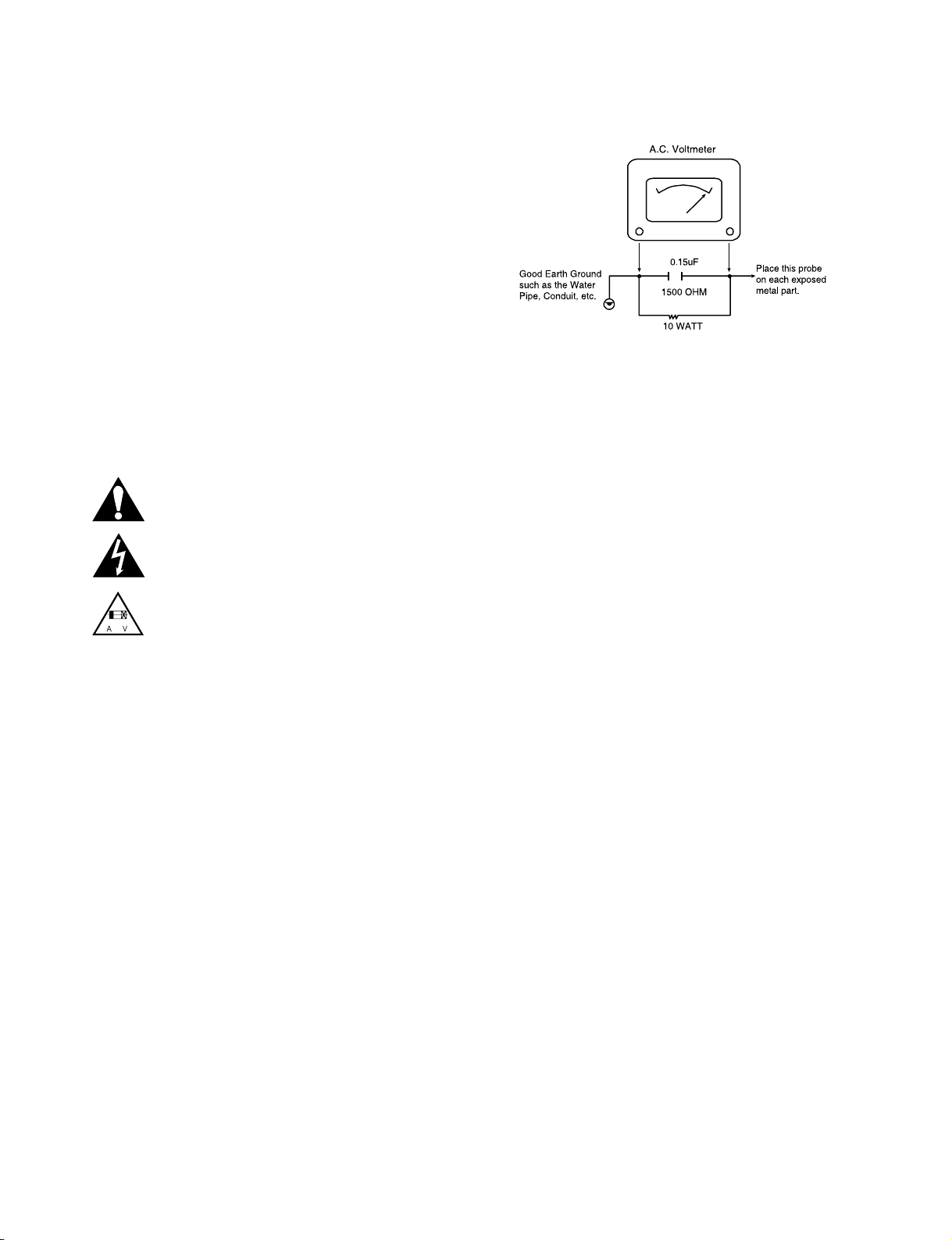
6. After reassembly of the set, always perform an AC leakage test on all exposed
metallic parts of the cabinet (the channel selector knobs, antenna terminals,
handle and screws) to be sure that set is safe to operate without danger of
electrical shock. DO NOT USE A LINE ISOLATION TRANSFORMER DURING
THIS TEST. Use an AC voltmeter having 5000 ohms per volt or more sensitivity
in the following manner: Connect a 1500 ohm, 10 watt resistor, paralleled by a .15
mfd 150V AC type capacitor between a known good earth ground water pipe,
conduit, etc.) and the exposed metallic parts, one at a time. Measure the AC
voltage across the combination of 1500 ohm resistor and .15 mfd capacitor.
Reverse the AC plug by using a non-polarized adaptor and repeat AC voltage
measurements for each exposed metallic part. Voltage measured must not
exceed 0.75 volts RMS. This corresponds to 0.5 milliamp AC. Any value
exceeding this limit constitutes a potential shock hazard and must be corrected
immediately.
TIPS ON PROPER INSTALLATION
1. Never install any receiver in a closed-in recess, cubbyhole, or closely fitting shelf
space over, or close to, a heat duct, or in the path of heated air flow.
2. Avoid conditions of high humidity such as: outdoor patio installations where dew
is a factor, near steam radiators where steam leakage is a factor, etc.
3. Avoid placement where draperies may obstruct venting. The customer should also
avoid the use of decorative scarves or other coverings that might obstruct
ventilation.
4. Wall- and shelf-mounted installations using a commercial mounting kit must follow
the factory-approved mounting instructions. A product mounted to a shelf or
platform must retain its original feet (or the equivalent thickness in spacers) to
provide adequate air flow across the bottom. Bolts or screws used for fasteners
must not touch any parts or wiring. Perform leakage tests on customized
installations.
5. Caution customers against mounting a product on a sloping shelf or in a tilted
position, unless the receiver is properly secured.
6. A product on a roll-about cart should be stable in its mounting to the cart.
Caution the customer on the hazards of trying to roll a cart with small casters
across thresholds or deep pile carpets.
7. Caution customers against using extension cords. Explain that a forest of
extensions, sprouting from a single outlet, can lead to disastrous consequences to
home and family.
Page 5

1-4
SERVICING PRECAUTIONS
CAUTION: Before servicing the PORTABLE DVD covered
by this service data and its supplements and addends, read
and follow the SAFETY PRECAUTIONS. NOTE: if
unforeseen circumstances create conflict between the
following servicing precautions and any of the safety
precautions in this publications, always follow the safety
precautions.
Remember Safety First :
General Servicing Precautions
1.Always unplug the PORTABLE DVD AC power cord from
the AC power source before:
(1) Removing or reinstalling any component, circuit board,
module, or any other assembly.
(2) Disconnecting or reconnecting any internal electrical
plug or other electrical connection.
(3) Connecting a test substitute in parallel with an
electrolytic capacitor.
Caution : A wrong part substitution or incorrect polarity
installation of electrolytic capacitors may result in an
explosion hazard.
2.Do not spray chemicals on or near this PORTABLE DVD
or any of its assemblies.
3.Unless specified otherwise in this service data, clean
electrical contacts by applying an appropriate contact
cleaning solution to the contacts with a pipe cleaner,
cotton-tipped swab, or comparable soft applicator.
Unless specified otherwise in this service data, lubrication
of contacts is not required.
4.Do not defeat any plug/socket B+ voltage interlocks with
which instruments covered by this service manual might
be equipped.
5.Do not apply AC power to this PORTABLE DVD and / or
any of its electrical assemblies unless all solid state device
heat sinks are correctly installed.
6.Always connect the test instrument ground lead to an
appropriate ground before connecting the test instrument
positive lead. Always remove the test instrument ground
lead last.
Insulation Checking Procedure
Disconnect the attachment plug from the AC outlet and turn
the power on. Connect an insulation resistance meter (500V)
to the blades of the attachment plug. The insulation
resistance between each blade of the attachment plug and
accessible conductive parts (Note 1) should be more than
1Mohm.
Note 1: Accessible Conductive Parts include Metal panels,
Input terminals, Earphone jacks,etc.
Electrostatically Sensitive (ES) Devices
Some semiconductor (solid state) devices can be damaged
easily by static electricity. Such components commonly are
called Electrostatically Sensitive (ES) Devices. Examples of
typical ES devices are integrated circuits and some field
effect transistors and semiconductor chip components.
The following techniques should be used to help reduce the
incidence of component damage caused by static electricity.
1.Immediately before handling any semiconductor
component or semiconductor-equipped assembly, drain off
any electrostatic charge on your body by touching a known
earth ground. Alternatively, obtain and wear a
commercially available discharging wrist strap device,
which should be removed for potential shock reasons prior
to applying power to the unit under test.
2.After removing an electrical assembly equipped with ES
devices, place the assembly on a conductive surface such
as aluminum foil, to prevent electrostatic charge buildup or
exposure of the assembly.
3.Use only a grounded-tip soldering iron to solder or
unsolder ES devices.
4.Use only an anti-static solder removal device. Some solder
removal devices not classified as “anti-static” can generate
electrical charges sufficient to damage ES devices.
5.Do not use freon-propelled chemicals. These can generate
an electrical charge sufficient to damage ES devices.
6.Do not remove a replacement ES device from its
protective package until immediately before you are ready
to install it. (Most replacement ES devices are packaged
with leads electrically shorted together by conductive
foam, aluminum foil,or comparable conductive material).
7.Immediately before removing the protective material from
the leads of a replacement ES device, touch the protective
material to the chassis or circuit assembly into which the
device will be installed.
Caution: Be sure no power is applied to the chassis or
circuit, and observe all other safety precautions.
8.Minimize bodily motions when handling unpackaged
replacement ES devices. (Normally harmless motion such
as the brushing together of your clothes fabric or the lifting
of your foot from a carpeted floor can generate static
electricity sufficient to damage an ES device.)
Page 6

1-5
SPECIFICATIONS
• DVD PLAYER
Power supply DC 12V (AC adapter terminal), DC 7.4V (Battery)
Power consumption 12W with battery
Weight 190.4g (0.56kg)(without battery pack)
External dimensions(W X D X H) (191 X 74 X 39mm)
Signal system NTSL
Laser Semiconductor laser, wavelength 655nm (DVD),
790nm(CD)
Frequency range (audio) DVD linear sound:48kHZ sampling 4HZ to 20kHZ
96KHZ sampling 4HZ to 44kHZ
Signal-to-noise ratio(audio) More than 85dB
Dynamic range(audio) More than 85dB
Harmonic distortion(audio) 0.08%
Operatingconditions(audio) Temperature: 41°F to 95°F, Operation status: Horizontal
• CONNECTORS
Video input/output(VIDEO IN/OUT) ø2.6x7.8(10/0, 10BC +28/0.10BC) *3F L=1200MM
Audio input/output 2.0Vrms (1 KHZ,0 dB), ø3.5m X 1
(AUDIO IN/OUT, analog audio)
Earphone terminal ø3.5mm stereo mini jack X 1
• LIQUID CRYSTAL DISPLAY
Panel size 7inches (16:9)
Projection system TN color transmission
Driving system TFT active matrix
• SUPPLIED ACCESSORIES
RC Aaudio/Video cable 1
AC Adapter (AD-DP40) 1
Power Cord 1
Battery Pack (DP-BT50) 1
Remote control 1
Battery for Remote control (Lithium) 1
Page 7

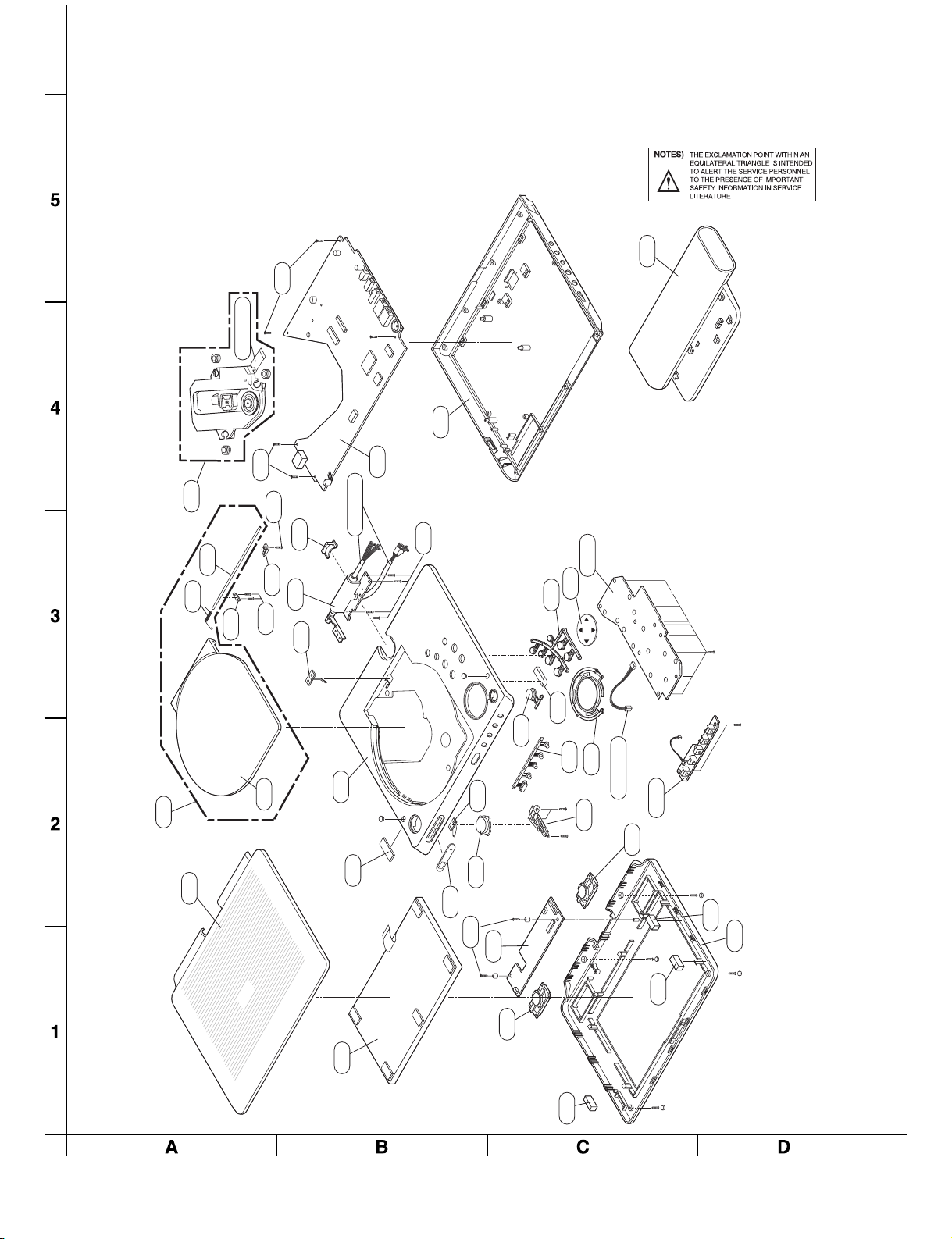
2-1
SECTION 2
EXPLODED VIEWS
CONTENTS
EXPLODED VIEWS .....................................................................................................................................2-2
1. CABINET AND MAIN FRAME SECTION ..................................................................................................2-2
3. PACKING ACCESSORY SECTION...........................................................................................................2-3
Page 8
2-2
A48
274
293
260
286
275
281
454
455
A00
455
A53
296
295
298
297
451
279
278
284
285
CABLE1
453
262
267
251
252
253
272
277
A51
261
264
277
A46A
A45A
FRONT
BOARD
LCD
BOARD
KEY
BOARD
MAIN BOARD
283
809
A42
A46
CABLE3
453
266
EXPLODED VIEWS
1. CABINET AND MAIN FRAME SECTION
CABLE2
A40
Page 9
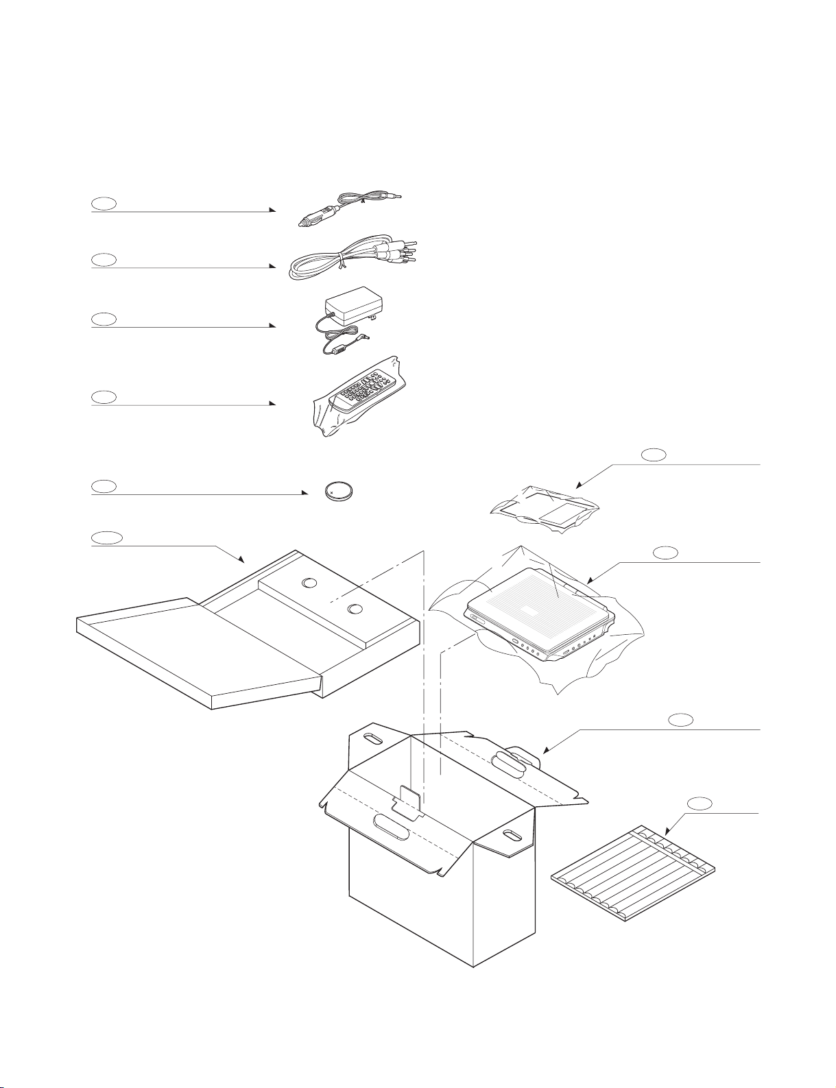
2-3
2. PACKING ACCESSORY SECTION
834 CABLE, CIJAR JACK
806 PLUG ASS'Y
833 ADAPTER
900 REMOTE CONTROL
808 BATTERY
801 OWNER'S MANUAL
802A BOX INNER
804 PACKING SHEET
802 BOX CARTON
803 PACKING
Page 10

3-1
SECTION 3
ELECTRICAL
CONTENTS
LCD PART ...................................................................................................................................................3-2
LCD ELECTRICAL TROUBLESHOOTING GUIDE .........................................................................3-3
BLOCK DIAGRAM......................................................................................................................................3-5
CIRCUIT DIAGRAM ...................................................................................................................................3-7
PRINTED CIRCUIT DIAGRAM ...............................................................................................................3-9
MAIN PART ...............................................................................................................................................3-11
MAIN ELECTRICAL TROUBLESHOOTING GUIDE .....................................................................3-11
1. POWER (DC-DC CONVERTER) CIRCUIT..........................................................................................3-11
2. MPEG CIRCUIT ...................................................................................................................................3-14
3. RF/SERVO CIRCUIT............................................................................................................................3-15
DETAILS AND WAVEFORMS ON SYSTEM TEST AND DEBUGGING .................................3-19
1. SYSTEM 27MHZ CLOCK, RESET & FLASH R/W SIGNAL................................................................3-19
2. SDRAM CLOCK ...................................................................................................................................3-19
3. DISC TYPE JUDGEMENT WAVEFORM .............................................................................................3-20
4. FOCUS ON WAVEFORM.....................................................................................................................3-22
5. SPINDLE CONTROL WAVEFORM (NO DISC CONDITION)..............................................................3-22
6. TRACKING CONTROL RELATED SIGNAL (SYSTEM CHECKING) ..................................................3-23
7. MT1389 AUDIO OPTICAL AND COAXIAL OUTPUT (ASPDIF) ..........................................................3-24
8. MT1389 VIDEO OUTPUT WAVEFORM ..............................................................................................3-24
9. AUDIO OUTPUT FROM AUDIO DAC ..................................................................................................3-25
WIRING CONNECTION DIAGRAMS..................................................................................................3-26
1. WIRING CONNECTION DIAGRAM 1..................................................................................................3-26
2. WIRING CONNECTION DIAGRAM 2..................................................................................................3-27
BLOCK DIAGRAMS.................................................................................................................................3-28
1. OVERALL BLOCK DIAGRAM..............................................................................................................3-28
2. POWER BLOCK DIAGRAM.................................................................................................................3-29
3. SERVO BLOCK DIAGRAM..................................................................................................................3-30
4. SYSTEM BLOCK DIAGRAM................................................................................................................3-31
5. AV BLOCK DIAGRAM ..........................................................................................................................3-32
CIRCUIT DIAGRAMS ..............................................................................................................................3-33
1. MPEG CIRCUIT DIAGRAM .................................................................................................................3-33
2. MEMORY CIRCUIT DIAGRAM............................................................................................................3-35
3. OPU & MOTOR CIRCUIT DIAGRAM ..................................................................................................3-37
4. AV CIRCUIT DIAGRAM........................................................................................................................3-39
5. CHARGE CIRCUIT DIAGRAM.............................................................................................................3-41
6. FM-TX (OPTION) CIRCUIT DIAGRAM................................................................................................3-43
7. PANEL I/F CIRCUIT DIAGRAM ...........................................................................................................3-45
8. MENU KEY CIRCUIT DIAGRAM .........................................................................................................3-47
9. FRONT KEY CIRCUIT DIAGRAM .......................................................................................................3-49
• CIRCUIT VOLTAGE CHART ..............................................................................................................3-51
PRINTED CIRCUIT DIAGRAMS ..........................................................................................................3-55
1. MAIN P.C.BOARD ................................................................................................................................3-55
2. KEY MENU P.C.BOARD ......................................................................................................................3-59
3. KEY FRONT P.C.BOARD.....................................................................................................................3-59
Page 11
3-2
LCD PART
1) Power measuring
Measure each power after power supply.
C902(-) : -10V, C901(+) : +15V, C916(+) : +7.5V, C918(+) : +5VD, C914 : 3.3V
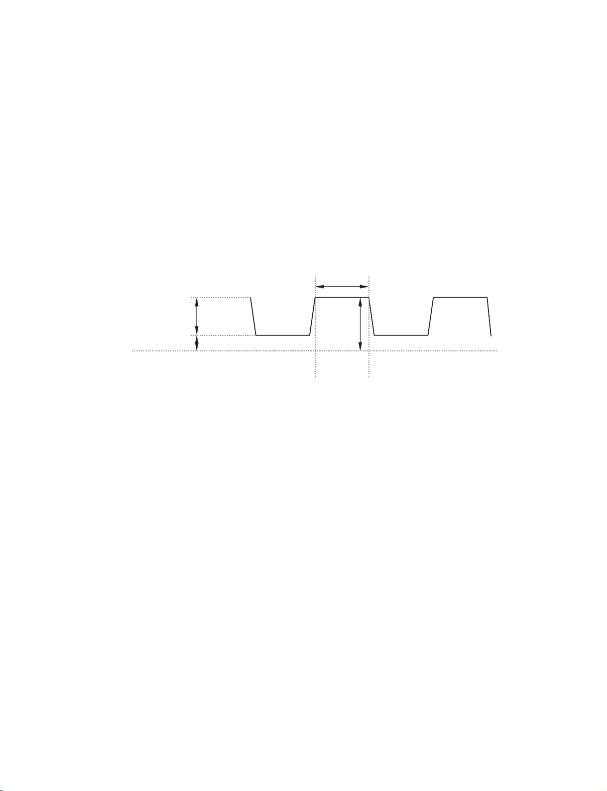
2) VCOM waveform adjustment
Adjust the VCOM level while changing the VR901 as below waveform by using the scope in the
C921.
Vcom Waveform
0.17V
3.72V
68.22µs
3.89V
GND
Page 12
3-3
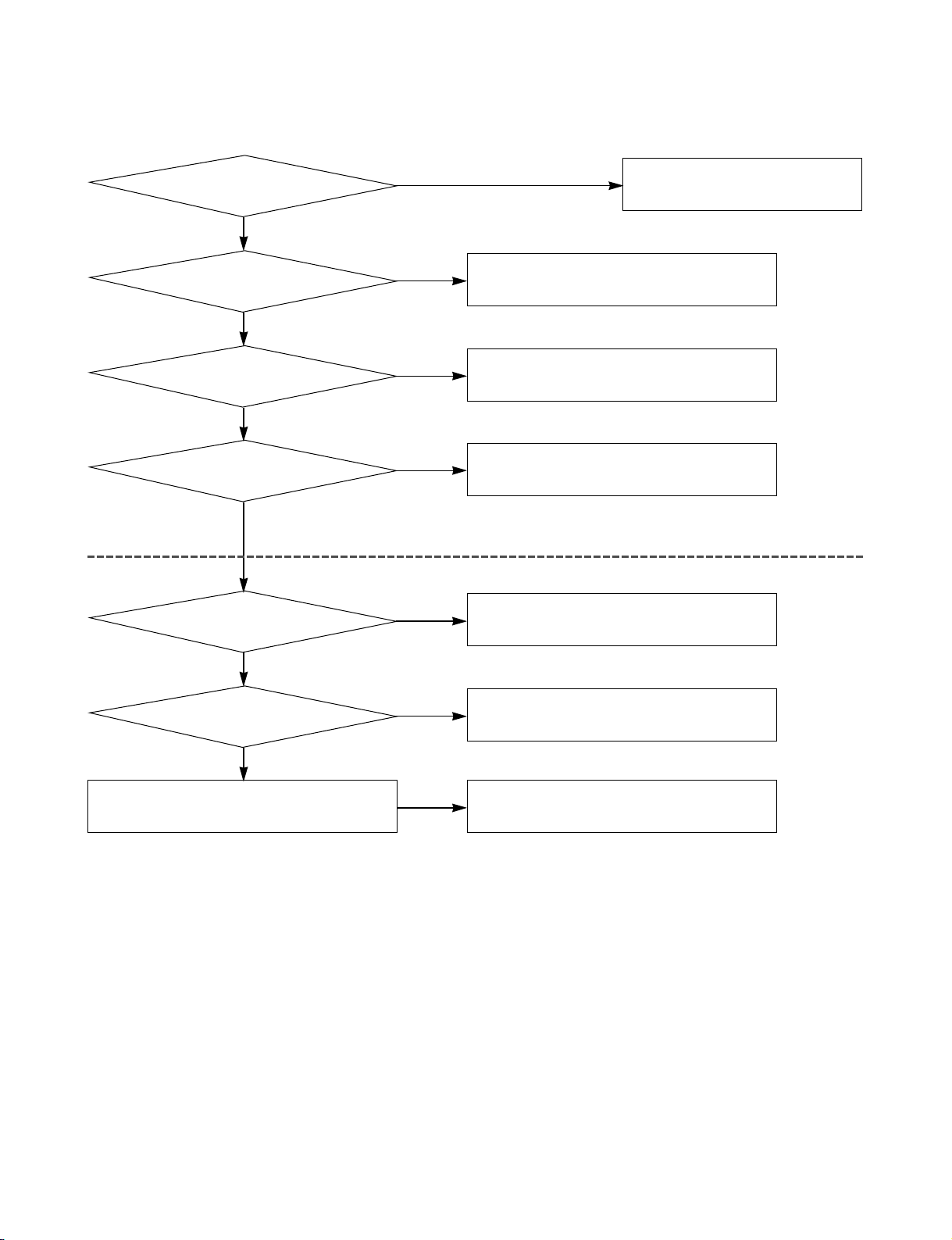
LCD ELECTRICAL TROUBLESHOOTING GUIDE
Fuse normal?
Fuse Replace
YES
YES
NO
Display condition?
Inverter abnormal
NO
Appear shadow form
interference in black background
IC(U1) normal operate
IC(U1) Check and Replace
YES
NO
+5V normal?
IC(U901) Check and Replace
YES
YES
NO
7.5V, 15V, -10V normal?
D907, D901, D902
NO
Main B/D on located
RGB signal output?
Check and Replace
MPEG1389. (Pin : 184, 185, 187)
YES
NO
IC(U902) and ReplaceVCOM signal? (4.5V)
NO
Page 13
3-4
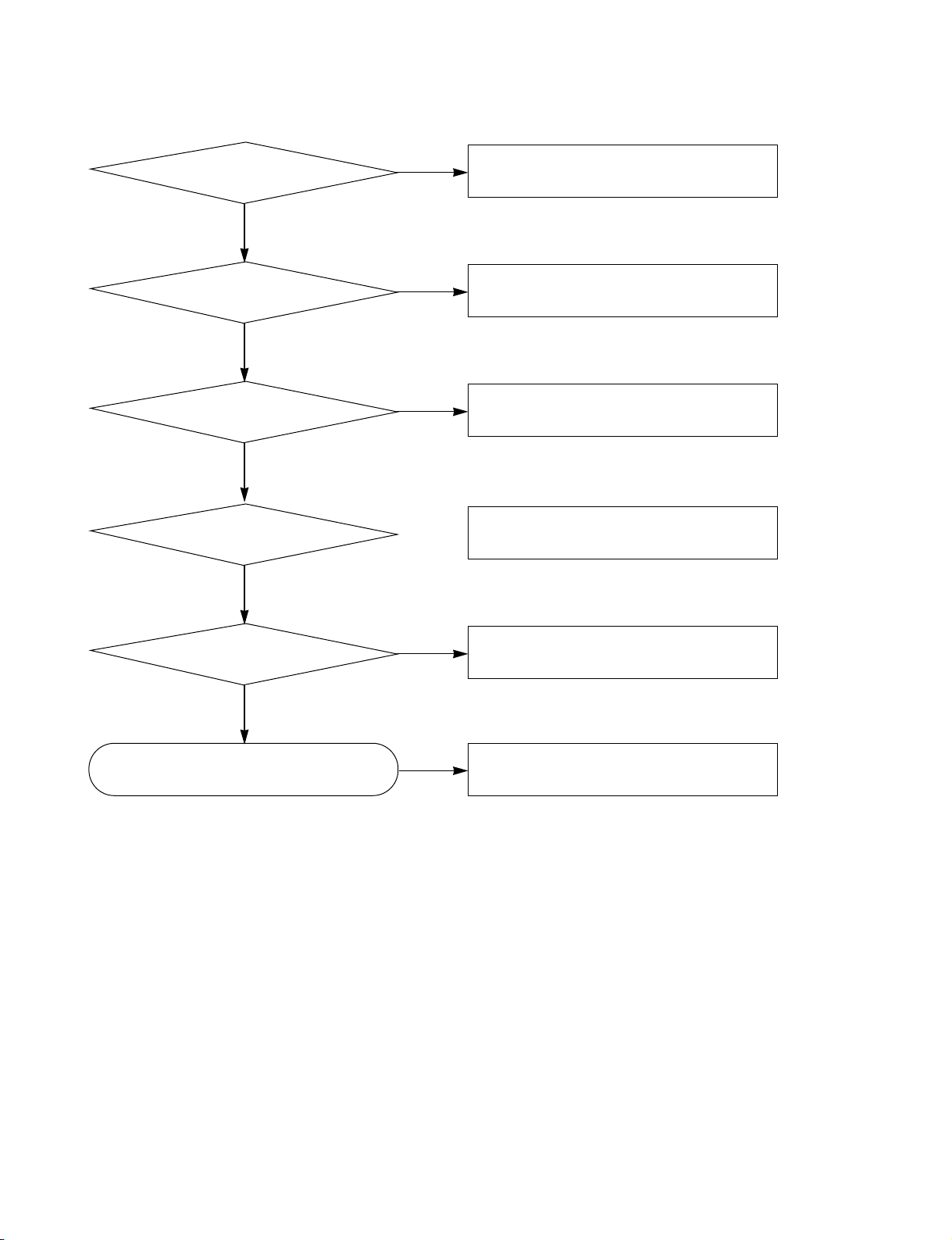
LCD ELECTRICAL TROUBLESHOOTING GUIDE
LCD MODE CONT signal?
All “LOW” (Normal condition?
MAIN B/D Check
YES
NO
TFT LCD pressure voltage?
+15V, -14V, +5V
Power source and D901, D902, U901 Check
YES
NO
TFT LCD normal?
Replace
YES
NO
Color adjusting normal?
Readjust as adjustement standard
YES
Each connector?
Replace and Reassemble
YES
NO
ReplaceEND
NO
Page 14
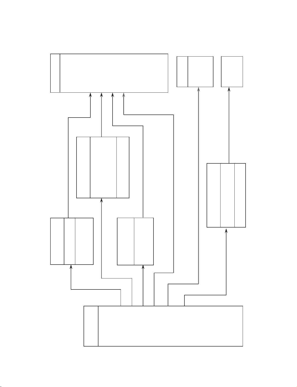
3-5
•VGH
BLOCK DIAGRAM
•VGL
•STVR
•STVL
LCD PANEL
•CKV
•SP L-
•SP L+
•SP R -
•MOD
•OE H
•STHL
•STHR
•CPH 3
•CPH 2
•CPH 1
•89P_R
•89P_G
•UND
•OEV
•VC O M O
•LNR
•89P_B
SPEAK
•SP R +
BACKLIGHT
•VG H (15V)
LCD POWER BLOCK
•VCOM
VCOM BLOCK
•NJM3414A IC
•VOLTAGE SUPPLY
SMOTHLY
•VG L (-1 0V)
•7.5V
•5V
•MP1540 IC
•BAT_OUT
•PWRCTL_LCD
•MP2359 IC
INVERTER POWER BLOCK
•ROUT
•GOUT
BLOCK
•BOUT
R/G/B Circuit
Connector
•STVR
(Main interface)
•STVL
•CKV
•UND
•OEV
•VC OMO
•LNR
•MOD
•OEH
•STHL
•STHR
•CPH3
•CPH2
•CPH1
•89P_R
•89P_G
•89P_B
•SP L-
•SP L+
•SP R -
•SP R +
•3.3V
•BAT_OUT
•PW R C T L _L C D
Page 15

3-6
MEMO
Page 16
3-7 3-8
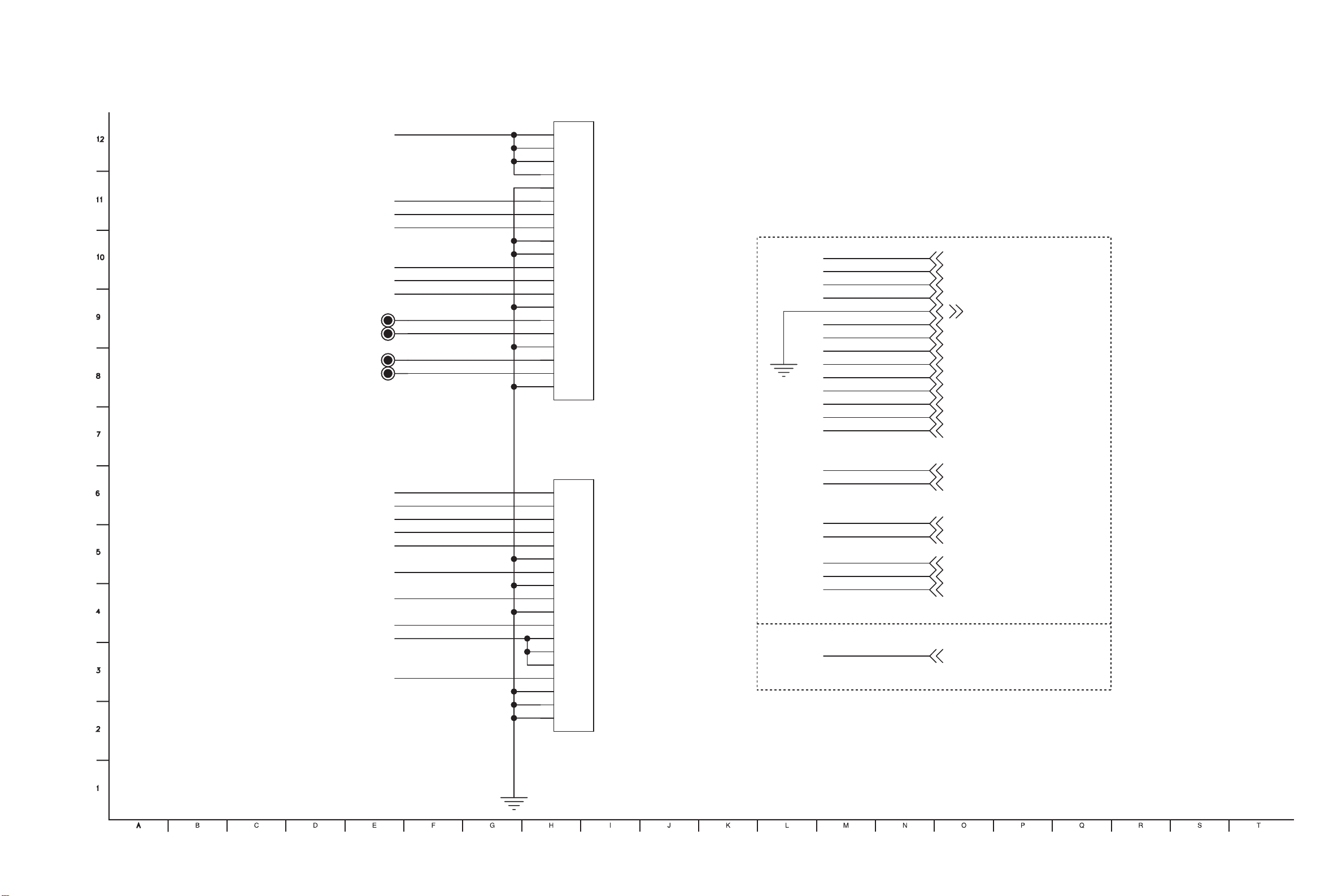
CIRCUIT DIAGRAM
TP701TP701
TP703TP703
TP702TP702
TP704TP704
3.3V
89P_R
89P_G
89P_B
CPH1
STHL
STHR
SP_RSP_R+
SP_LSP_L+
J701
J701
20
19
18
17
16
15
14
13
12
11
10
9
8
7
6
5
4
3
2
1
CON20
CON20
OFF-PAGE CONNECTION
SP_LSP_L+
SP_RSP_R+
GND
STVR
STVL
CKV
UND
OEV
LNR
OEH
STHL
STHR
SP_LSP_L+
SP_RSP_R+
STVR
STVL
CKV
UND
OEV
LNR
OEH 2
STHL
STHR
GND
5
5
5
5
2,3,4,5,6,8
2
2
2
2
2
2
2
2
STVR
STVL
CKV
UND
OEV
VCOMO
LNR
OEH
BAT_OUT
PWRCTL_LCD
J702
J702
18
17
16
15
14
13
12
11
10
9
8
7
6
5
4
3
2
1
CON18
CON18
CPH1
VCOMO
BAT_OUT
PWRCTL_LCD
89P_R
89P_G
89P_B
PANEL T-CON I/F
3.3V
3.3V
TO SERVO
LG & MALATA
LG & MALATA
LG & MALATA
Document Number
Document Number
Document Number
07.LCD I/F
07.LCD I/F
07.LCD I/F
Monday, January 15, 2007
Monday, January 15, 2007
Monday, January 15, 2007
CPH1
VCOMO
BAT_OUT
PWRCTL_LCD
89P_R
89P_G
89P_B
2
2
4,6
2
2
2
2
2,3,4,8
Page 17

3-9 3-10
PRINTED CIRCUIT DIAGRAM
(TOP VIEW)
(BOTTOM VIEW)
MEMO
Page 18

3-11
MAIN PART
MAIN ELECTRICAL TROUBLESHOOTING GUIDE
No power on
by ADAPTOR
A
Replace ADAPTOR
NO
YES
1. POWER (DC-DC CONVERTER) CIRCUIT
Is ADAPTOR
out 9.5V
Replace D606
NO
NO
YES
YES
Is D606 OK.
Replace U202
Replace U401 Replace JK902
No +3.3V No +5V No LCD powerNo +18V
YES
YES
Is U202
3.3V OK?
NO
Replace U401
Is U401
3.3V OK?
YES
No power on
by BATTERY
A
Replace BATTERY
NO
YES
Is
BATTERY OK?
YES
A
Page 19

3-12
Audio out abnormal
Check Audio jack & mode
YES
YES
Check +9V
YES
Check signals from MPEG
YES
Replace IC(U504)
MAIN ELECTRICAL TROUBLESHOOTING GUIDE
Audio in/speaker
abnormal
Replace IC(U502)
Replace
Q501 and Q503
Check Audio jack &
mode S/W
NO
YES
YES
Is Q501
and Q503 OK.
Speakers
NO
YES
YES
Is speakers OK.
Replace
B. AUDIO OUT ABNORMAL
D. AUDIO IN/SPEAKER ABNORMAL
Video in abnormal
Refer to LCD part
Replace
(U501 IC)
Check Video jack
& mode
NO
YES
YES
Is U501 OK.
Check
R203, R202, C202
YES
YES
E. VIDEO IN ABNORMAL
Video out abnormal
Check Video jack & mode
YES
YES
Check Video signals from MPEG
YES
Check IC(U501)
YES
Check LC filter
C. VIDEO OUT ABNORMAL
Page 20

3-13
OPEN/CLOSE abnormal
Check SW401, SW402 switch
Refer to SERVO part.
YES
YES
Check IC(U201) Pin 130
Check the connectin of MD.
YES
Refer to SERVO part.
YES
NO
MAIN ELECTRICAL TROUBLESHOOTING GUIDE
Picture abnormal
Check the disc.
YES
YES
Refer to SERVO part
YES
Check MPEG_CLK
Signal of MPEG part
YES
Check MPEG (IC U201)
YES
Replace B/D
F. PICTURE ABNORMAL
H. OPEN/CLOSE ABNORMAL
Disc error
Check Disc
YES
YES
Refer to SERVO part
YES
YES(If OK)
YES(If OK)
YES(If OK)
(If OK)
Replace B/D
G. DISC ERROR
Page 21

3-14
MAIN ELECTRICAL TROUBLESHOOTING GUIDE
2. MPEG CIRCUIT
Power is on
END
YES
YES
YES
OK
Check power & clock.
Does Logo appear
on the screen?
NO
Check CD/DVD DSP
output signal.
Check MPEG Decoder
input signal.
NO
OK
Does the
Video of the DVD Disc
play properly?
Is MPEG data
signal normal?
NO
YES
Check CD/DVD DSP
output signal.
Check MPEG Decoder
input signal.
NO
Is error
signal normal?
YES
OK
Check CD/DVD DSP
output signal.
Check MPEG Decoder
input signal.
NO
Does the
Video of the video CD
play properly?
Is MPEG data
signal normal?
NO
Check clock signal
NO
Does
the audio sound output
normally?
Does the audio
signal output from MPEG
decoder?
NO
Check clock signal
NO
Is Clock normal?
YES
YES
YES
YES
OPTION
If included VCD function.
Page 22

3-15
MAIN ELECTRICAL TROUBLESHOOTING GUIDE
3. RF/SERVO CIRCUIT
Laser off
Check the RFL connection
between J401 and MT1389.
Put Disc in.
NO
Check the related circuit on
MT1389 RFL signal .
NO
Disc ID is correct?
Proper RFL signal
on MT1389?
NO
YES
YES
YES
Check the cable connection
between spindle and main PCBA.
Check DMSO related circuit
on MT1389.
NO
Does spindle rotate.
Proper DMSO signal
on MT1389
NO
YES
Replace IC(U201)
YES
D
YES
Page 23

3-16
MAIN ELECTRICAL TROUBLESHOOTING GUIDE
Check IC(U401)
Check connections between
MT1389 and pick-up head.
NO
Focus on OK.
Proper
signals on A, B, C, D
of MT1389
NO
YES
Check the related circuit
on MT1389 FEO sugnal.
NO
Proper FEO signal
on MT1389.
YES
YES
Check cable connection on
pick-up head.
Check the related circuit
on MT1389
NO
Track on OK.
Proper FEO signal
on MT1389.
NO
Disc is play?
NO
YES
Check the TRSO connection
on MT1389 and motor dirver.
NO
Properly TRSO signal
on MT1389.
YES
Check the tracking control
amp circuit on motor driver.
T+ & T-
output properly.
YES
Check RF signal waveform.
YES
YES
E
D
YES
YES
Page 24

3-17
MAIN ELECTRICAL TROUBLESHOOTING GUIDE
Check Audio filter, amplify,
mute circuit.
Check Aout_L related circuit
Aout_R
NO
Normal
Audio output when
disc playback.
Proper
Aout_L, Aout_R signal
on MTK1389
NO
Check the related circuit of
Audio DAC.
NO
YES
YES
Check communi cation lines
on MT1389
NO
Normal
IR. VFD & Front pannel
key functions.
Commu-
nications between
IR.VFD Front pannel key &
MT1389 & Front µ-com
is normally.
NO
NO
YES
Check the cable connection
on Front pannel.
TEST END
YES
E
YES
Page 25

3-18
MAIN ELECTRICAL TROUBLESHOOTING GUIDE
Is U603 OK?
No turn on Red LED Is 8.4V of J602_Pin 1 OK?
YES
Replace IC(U603).
NO
Is L601 OK?
Replace L601.
YES
NO
Is IC(U601) OK?
Replace IC(U601).
YES
NO
Is L602 OK?
Replace L602.
YES
NO
NO
* CHARGEING CIRCUIT
Page 26

3-19
DETAILS AND WAVEFORMS ON SYSTEM TEST AND DEBUGGING
1. SYSTEM 27MHz CLOCK, RESET & FLASH R/W SIGNAL
1) MT1379 main clock is at 27MHz (X201)
FIG 1-1
2. SDRAM CLOCK
1) MT1389 main clock is at 27MHz (R308)
FIG 2-1
U301 PIN38
DCLK=125MHz, Vp-p=3.7V
Page 27

3-20
3. DISC TYPE JUDGEMENT WAVEFORM
FIG 3-1
FIG 3-2
F+(U401 PIN8)
F+(U401 PIN8)
FE(U201 PIN26)
FE(U201 PIN26)
RFL(U201 PIN21)
RFL(U201 PIN21)
Page 28

3-21
FIG 3-3
FIG 3-4
F+(U401 PIN8)
F+(U401 PIN8)
FE(U201 PIN26)
FE(U201 PIN26)
RFL(U201 PIN21)
RFL(U201 PIN21)
Page 29

3-22
4. FOCUS ON WAVEFORM
5. SPINDLE CONTROL WAVEFORM (NO DISC CONDITION)
FIG 4-1
FIG 5-1
FOSO(U401 PIN11)
DMSO(U401 PIN12)
F+(U401 PIN8)
SP-(U401 PIN15)
F-(U401 PIN9)
SP+(U401 PIN14)
Page 30

3-23
6. TRACKING CONTROL RELATED SIGNAL (SYSTEM CHECKING)
FIG 6-1
FIG 6-2
TE(U201 PIN27)
TE(U201 PIN27)
TRSO(U401 PIN23)
TRSO(U401 PIN23)
T-(U401 PIN18)
T+(U401 PIN17)
T-(U401 PIN18)
T+(U401 PIN17)
Page 31

3-24
7. MT1389 AUDIO OPTICAL AND COAXIAL OUTPUT (ASPDIF)
FIG 7-1
FIG 8-1
(U201 PIN208)
ASDIF Vpp=2.5V
(U501 PIN14)
8. MT1389 VIDEO OUTPUT WAVEFORM
1) Full colorbar signal (CVBS)
Page 32

3-25
FIG 9-1
(JK601 PIN4, 5)
MR 1kHz 0dB
9. AUDIO OUTPUT FROM AUDIO DAC
1) Audio L/R
2) Audio related Signal
ASDAT0(IC301 PIN3)
ABCK(IC301 PIN4)
ALRCK(IC5301 PIN5)
ASDATA3
FIG 9-2
Page 33

3-26
WIRING CONNECTION DIAGRAMS
1. WIRING CONNECTION DIAGRAM 1
(MAIN PCB <---> LCD PCB)
MAIN PCB
MAIN PCB
Page 34

3-27
2. WIRING CONNECTION DIAGRAM 2
(MAIN PCB <---> KEY PCB)
MAIN PCB
Key PCB
Page 35

3-28
BLOCK DIAGRAMS
1. OVERALL BLOCK DIAGRAM
System & AV Part
16KBit
EEPROM
3.3V
64MBit
SDRAM
3.3V3.3V
R#
FLASH
MEMORY
8/16/32MBit
LCD PANEL
3.3V/BAT_OUT
2F2301P
3.3V FM+3.3V
N
/AV_JACK_I
FM+3.3V
FM_MUTE
SDA
SCL
DQ[0..15]
DCLK,DCKE
WE#,DQM[0..1]
CS#,CAS#,RAS#,
MA[0..11], BA[0..1],
AD[0..7]
PCE#,PRD#,PW
A[0..21]
CKV,PWRCTL_LCD
OEH/V,LNR,UND,
STHL/R, STVL/R,
MOD,89P_R/G/B,
VCOMO,CPH1/2/3,
1.8V/3.3V
O
XI,X
SPK
H/P
SP_L/R-
UTE
SP_M
MPEG
COAXIAL
USB JACK
A+5V
A-5V
FSAV330
A+5V
M
N
BS
CV
VIDEO_IO_CTL
CVBS_I
USBP,USB
SDI
CH_SCS,
SCLK,
SDO
GT6319
/M_RESET
5VA
AD_I
PWM
AD_T
AD_U
AD_PR
STANDBY
ASPDIF
TPS60400
A+5V
D
RED,
GREEN
Power,
Charge LE
R
IR
RECEIVE
REMOCON
AD_K1,
AD_K2
KEY
AV IN/OUT
-
SP_L/R+/
ML/R_OUT
A± 5V
PEN
TRO
VOLUME
PT2303
A+5V
NJM4580M
A_MUTE_SW
AOUT_L/R
MT1389P
OPO
LIMIT
OP-,OP+
BH1418FV
O
FM_SCS,SCLK,SD
DISC
27MHz
LDO1,LDO2,IOA,V20
A,B,C,D,E,F,RFO,MDI1/2
UP
PICK
M
MOTOR
SPINDLE
SLED
R
MOTO
V
A+5V
LD_5
M5V
2F2301P
V1P4,FOSO,TRSO,FMSO,DMSO,STBY
5VA
F+,F-,
T+,T-
-
SP+,
SP
SL-
M5V
AM5898N
DC-DC BLOCK1
MOTOR DRIVER
SL+,
M
DECK MECHANISM
1.8V
CM1117
3.3V
DC-DC BLOCK2
BAT_OUT
FDS4435
SI4335
P+
DC_IN
P-
BATTERY
Page 36

3-29
2. POWER BLOCK DIAGRAM
in
BAT
ou
SW
(9V
i
Cha
rge
E
na
ble
Cha
rge
The
rmi
st
DC
Sen
se
BAT
Se
ns
Pow
er
CT
5VA
5V
3.3
1.8
DVB
3.
3V
SW(
TU/
DV
D5V
-5V
Sta
ndb
Sta
ndb
Sta
ndb
5VA
5V
3.3
1.8
-5V
3.3
7.5
15V
-10
D5V
7.5
15V
-10
D5V
5VA
DVB
5V
SW(
TU/
DV
D5V
5V
3.3
AAT
110
GT6
312
AP1
624
MP1
411
Charge
Discharge
LCD
Panel
Video
Audio
System
Servo
5VA
V
7.5
2
110
AAT
-5V
Voltage Inverter
y
ndb
Sta
V
3.3
V
1.8
V
-10
V
3.3
15V
Vcc
LCD
3V
3.
DVB
D)
DV
TU/
SW(
S/W
DC-DC
D5V
D5V
y
ndb
Sta
5V
V
1.8
Reg
V
3.3
V
V
15V
7.5
-10
624
AP1
t
ou
BAT
DC-DC
Reg
L
CT
er
Pow
e
ns
Se
BAT
Divide Divide
se
Sen
DC
n)
i
(9V
SW
312
GT6
9V in
BAT Con
FET
er
st
rge
rmi
Cha
The
ble
na
E
rge
Battery Charge Circuit
Cha
LCD Grid
5VA
DC-DC
D5V
D5V
y
ndb
Sta
S/W
411
MP1
5VA
5V
5V
DVB
S/W
V
-5V
3.3
5V
D)
DV
TU/
SW(
DC-DC
AC/DC Adapter
Page 37

3-30
3. SERVO BLOCK DIAGRAM
Spi
dle
Mo
Steppi
ng
Mo
L
X501
27MHz
X-TA
IC201
MTK1389P
P-DVDPLAYER
ONE CHIP
FMSO,DMSO,FOSO,
V1P4
TRSO,STBY,
ALPC
Driverv
IC401
AM5898N
DVD : A,B,C,D,RF
F,RF
CD : A,B,C,D,E,
TR+, TR-
FO+, FO-,
SL-,SL+
LIMIT
IOA
MDI1,MDI2
CDLD(LD01),DVDLD(LD02)
ng
ter
PICK
UP
Mo
Steppi
Motor
SP-,SP+
ter
ndle
Mo
Spi
O
OP
OP+,OP-
Page 38

3-31
4. SYSTEM BLOCK DIAGRAM
2^20*8= 8Mbit
2^21*8=16Mbit
2^22*8=32Mbit
2^14*2^8*16=64Mbit
16KBit
EEPROM
3.3V
System & AV Part
SDA
SCL
27MHz
FLASH
MEMORY
3.3V
8/16/32MBit
A0~A19,AA20,AA21
AD0~AD7
3.3V
PCE#,PRD#,PWR#
MPEG
64MBit
SDRAM
KEY1
CS#,CAS#,RAS#
MA0~MA11,DBA0/1
DQ0~DQ15
WE#,DQM0,DQM1
DCLK,DCKE
AD_K1
SDI
CH_SCS,
SCLK,
SDO
KEY2
LCD MODE,DISPLAY,SETUP,MENU
UP,DOWN,LEFT,RIGHT,ENTER
AD_K2
GT3919
POWER,PLAY/PAUSE,REW,FF,STOP,
COLOR,BRIGHT,AV IN/OUT,LCD OPEN
RED,
GREEN
Power,
Charge LED
MT1389P
/M_RESET
5VA
1.8V/3.3V
USB JACK
A+5V
IR
RECEIVER
USBP,USBM
REMOCON
Page 39

3-32
5. AV BLOCK DIAGRAM
±
AV OUT PATH
AV IN PATH
System & AV Part
A+5V
VIDEO
FSAV330
AUDIO
< AV IN/OUT >
SP_L+/L-
A+5V
SPK
SP_R+/R-
PT2303
VOLUME
SPK
H/P JACK
SP_L-/R-
FM+3.3V
BH1418FV
ML_OUT,MR_OUT
JACK
COAXIAL
FM+3.3V
2F2301P
3.3V
V
3.3
1.8V/3.3V
/AV_JACK_IN
CVBS_IN
VIDEO ADC
CVBS
VIDEO_IO_CTL
5V
A±
NJM4580M
AOUT_L/R
2CH DAC
OP-AMP
A_MUTE_SW
SP_MUTE
FM_SCS,SCLK,SDO
FM_MUTE
MPEG
MT1389P
ASPDIF
Page 40

3-33 3-34
1. MPEG CIRCUIT DIAGRAM
CIRCUIT DIAGRAMS
1.8V
3.3V
L212 FBL212 FB
+
+
+
+
CE208
CE208
47uF/10V
47uF/10V
100uF/10V
100uF/10V
Chip Decoupling Cap.
R230
XO
X201
X201
27MHz
27MHz
C274
C274
33pF
33pF
Crystal
RFV33
89P_3V3
C231
C231
0.1uF
0.1uF
TP206TP206
TP210TP210
TP211TP211
TP207TP207
TP212TP212
L207
L207
FB
FB
L208
L208
FB
FB
FG IOA
R223
C253
CE209
CE209
C253
0.1uF
0.1uF
100KR230 100K
C275
C275
33pF
33pF
RFV18
C280
C280
0.1uF
0.1uF
AVDD18_VPLL
C243
C243
0.1uF
0.1uF
0R223 0
C255
C254
C255
C254
0.1uF
0.1uF
0.1uF
0.1uF
3.3V
XI
89P_3V3
1.8V
C244
C244
4.7uF
4.7uF
L201
L201
FB
FB
V2P8
+
+
CE205
CE205
47uF/6.3V
47uF/6.3V
B
A
D
C
RFO
LDO2
LDO1
RFV33
L209
L209
FB
FB
L210 FBL210 FB
C256
C256
0.1uF
0.1uF
C263
C263
0.1uF
0.1uF
+
CE210
+
CE210
100uF/6.3V
100uF/6.3V
C232
C232
0.1uF
0.1uF
C240
C236 120pF/NCC236 120pF/NC
R218
R222
C241
C241
0.1uF
0.1uF
TP223TP223
C246
C246
0.1uF
0.1uF
C249
C249
10uF/10V
10uF/10V
C257
C257
0.1uF
0.1uF
C268
C268
0.1uF
0.1uF
U202
U202
CM1117SCM233
CM1117SCM233
SOT223
SOT223
3
IN
R206
R206
6.8
6.8
+
+
1uFC238 1uF
C238
C239
1uFC240 1uF
C234
1uFC234 1uF
TP213TP213
TP214TP214
TP208TP208
TP215TP215
TP209TP209
TP225TP225
C247
C247
10uF/10V
10uF/10V
C258
C258
0.1uF
0.1uF
C269
C269
0.1uF
0.1uF
TAB
OUT
GND
1
Change 620->680
R233 330R233 330
C218
C218
0.1uF
0.1uF
V20
CE206
CE206
47uF/6.3V
47uF/6.3V
1uFC239 1uF
C235
MDI1
MDI2
0R218 0
0R222 0
TP218TP218
TP219TP219
TP220TP220
C245
C245
0.1uF
0.1uF
R224
C248 C/NCC248 C/NC
C250
C250
0.1uF
0.1uF
89P_3V3
TP224TP224
89P_3V3
C259
C259
0.1uF
0.1uF
C270
C270
0.1uF
0.1uF
4
2
R232
R232
680
680
C204
C204
0.01uF
0.01uF
1uFC235 1uF
TP216TP216
TP217TP217
TP221TP221
TP222TP222
1.8V
1.8V
L211 FBL211 FB
C260
C260
0.1uF
0.1uF
C271
C271
0.1uF
0.1uF
C205
C205
2200pF
2200pF
+
+
CE204
CE204
100uF/6.3V
100uF/6.3V
V1P4
C233
C233
0.1uF
0.1uF
C
D
A
B
SUBA
SUBB
E
F
R208 2KR208 2K
R209
V2P8
V20
V1P4
OPO
OP-
OP+
DMO
FMO
TRO
FOO
USBP
USBM
5.1KR224 5.1K
FG
LIMIT
A2
A3
A4
A5
A6
A7
A8
A18
A19
C251
C251
4.7uF
4.7uF
89P_3V3
C261
C261
0.1uF
0.1uF
1.8V
C272
C272
0.1uF
0.1uF
L213
L213
FB(1206)
FB(1206)
RFVDD3
PLLVDD3
+
+
CE207
CE207
47uF/6.3V
47uF/6.3V
C262
C262
0.1uF
0.1uF
C273
C273
0.1uF
0.1uF
C276
C276
0.1uF
0.1uF
2KR209 2K
C252
C252
0.1uF
0.1uF
10
11
12
13
14
15
16
17
18
19
20
21
22
23
24
25
26
27
28
29
30
31
32
33
34
35
36
37
38
39
40
41
42
43
44
45
46
47
48
49
50
51
52
53
54
55
56
57
58
59
60
61
62
63
64
1.8V
+
+
C277
C277
100uF/6.3V
100uF/6.3V
CM1117SCM223
C226
C226
0.1uF
0.1uF
1
AGND
2
DVDA
3
DVDB
4
DVDC
5
DVDD
6
DVDRFIP
7
MA
8
MB
9
MC
MD
SA
SB
SC / TNI
SD / TPI
MDI1
MDI2
LDO2
LDO1
SVDD3
CSO/RFOP
RFLVL / RFON
SGND
V2REFO
V20
VREFO
FEO
TEO
TEZISLV
OP_OUT
OP_INN
OP_INP
DMO
FMO
TROPENPWM
PWMOUT1 / V_ADIN0
TRO
FOO
AGND33_DMPLL
AVDD33_DMPLL
USB_DP
USB_DM
VDD33_USB
VSS33_USB
PAD_VRT
VDD18_USB
VSS18_USB
USB_XTALO / GPIO15
USB_XTALI / GPIO14
DVDD33
DVDD18
FG / GPIO16
DVSS33
DVSS18
IOA22 / GPIO18
DVDD18
IOA2
IOA3
IOA4
IOA5
IOA6
IOA7
HIGHA0
IOA18
IOA19
89P_3V3
4
31
2
RFVDD3
256
65
R207 15KR207 15K
AVDD3
DVDD33
R#
PW
1000pFC201 1000pF
750KR201 750K
+
ADACVDD
231
230
RFGND18
ADACVDD1
ADACVDD2
DVSS33
AD7
A17
91
90
A17
47KR225 47K
15KR228 15K
10KR229 10K
C208
C208
10uF/10V
10uF/10V
C216 4.7uFC216 4.7uF
AOUT_L
AOUT_R
228
229
227
AVCM
AL / SDATA2 / GPIO1
AR / SDATA0 / GPIO0
DVDD18
IOA0
UWR#94URD#95DVDD3396UP1_2 / GPIO1997UP1_3 / VSCK98UP1_4 / VSTB99UP1_5 / VSDA
93
92
1.8V
A0
FOO
TRO
FMO
DMO
226
C222 1500pFC222 1500pF
225
ADACVSS1
JITFNJITFO
ADACVSS2
SDI
224
223
APLLVSS
APLLCAP
SCLK
TP202TP202
+
C211 0.1uFC211 0.1uF
CE202 100uF/6.3V+CE202 100uF/6.3V
R214 100KR214 100K
AVDD18_VPLL
APLLVDD3
222
221
220
219
APLLVDD
VPLL_TST
AVDD18_VPLL
UP1_6 / SCL
100
101
102
SCS
SCL
SDA
CH_
SDO
J202
J202
USB TYPEA
USB TYPEA
AGND18_VPLL
UP1_7 / SDA
218
103
1:GND
1:GND
4:VCC
4:VCC
VFE_TSTP / AUDIO_IN1
UP3_0
2:D+
2:D+
3:D-
3:D-
89P_3V3
L204
L204
FB
FB
0.1uFC220 0.1uF
C220
217
216
AGND_VFE
VFE_TSTN / AUDIO_IN2
UP3_1
UP3_4 / RXD
104
105
RXD
89P_3V3
C221 4.7uFC221 4.7uF
CVBS_INP
215
213
214
CVBS_INP
AVDD33_VFE
CVBS_INN / BATTERY
UP3_5 / TXD
ICE
PRST#
106
107
108IR109
R231
R231
TXD
/M_RESET
56
1
1
2
2
3
3
4
4
10uF/10V/NC
10uF/10V/NC
2.2K
2.2K
1
2
3
4
212
L205
L205
FB
FB
AVDD33_ADC
211
110
FM_SCS
89P_3V3
C223
C223
0.1uF
0.1uF
210
209
AGND_ADC
DVDD33_ADC
GPIO22 / SD_DATA0 / INT0#
DQM0
111
112
E
FM_MUT
DQM0
C283
C283
1uF
1uF
C278
C278
PWRCTL_LCD
ASPDIF
208
207
206
DGND_ADC
SPDIF / GPIO23
GPIO11 (ASDATA4)
GGPIO12 (MCDATA)
GPIO21 / SD_CLK
RD7
RD6
RD5
113
114
115
DQ7
DQ6
DQ5
DQ4
Add R231 2.2K
Add C283 1uF
L214
L214
FB/NC
FB/NC
205
116
TE_SW
A_MU
R210
R210
204
DVDD18
RD4
117
DQ3
GPIO10 (ASDATA3)
RD3
89P_3V31.8V
C215
C215
3300pF
3300pF
470
470
TE
VIDEO_IO_CTL
/SP_MU
203
202
201
200
GPIO9 (ACLK)
GPIO8 (ABCK)
GPIO7 (ALRCK)
DVDD33
RD1
RD2
118
120
119
121
DQ2
DQ0
DQ1
R236
R235
L215
1
2
3
R234
R234
10K/NC
10K/NC
199
198
DVDD33
GPIO6 (ASDATA2)
RD15
RD0
122
123
4
DQ15
DQ1
AAT4610/NC
AAT4610/NC
VOUT
GND
SET
GPIO5 (ASDATA1)
RD14
VCOMO
DACVDD3
197
196
195
194FS193
VREF
DACVDDC
DACVSSC
VCOM / GPIO3
CVBS(Y)
GPIO4 (ASDATA0)
DACVDDB
DACVSSB
DACVDDA
DACVSSA
HSTR
HSTL
DVSS18
DVDD18
VSTU
VSTD
GPIO100
DVDD33
GPIO101
GPIO102
GPIO103
SD_D3
SD_D2
SD_D1
MS_D3
MS_D2
MS_D1
DVDD18
MS_CLK
MS_BS
MS_D0
DVDD33
DVSS33
RCLK
DVDD33
DVDD18
RCS#
RAS#
CAS#
RWE#
DQM1
DVDD33
GPIO20 / SD_CMD
RD13
RD12
RD11
RD9
RD10
MT1389P
MT1389P
124
125
126
128
127
QFP256A_0.4MM-MT1389
QFP256A_0.4MM-MT1389
22R236 22
22R235 22
FBL215 FB
U203
U203
5
VIN
4
ON
R215
R215
560
560
G
B
R
HCK
HOE
LR
VOE
UD
VCK
RA4
RA5
RA6
RA7
RA8
RA9
RA11
CKE
RA3
RA2
RA1
RA0
RA10
BA1
BA0
RD8
C279
C279
10uF/10V/NC
10uF/10V/NC
ADACVDD
APLLVDD3
DACVDD3DACVDD3
192
191
190
189
188
187
186
185
184
183
182
181
180
179
178
177
176
175
174
173
172
171
170
169
168
167
166
165
164
163
162
161
160
159
158
157
156
155
154
153
152
151
150
149
148
147
146
145
144
143
142
141
140
139
138
137
136
135
134
133
132
131
130
129
DQ9
DQ10
DQ11
DQ12
DQ13
USBP
USBM
A+5V
C230
C230
0.1uF
0.1uF
C212
C212
0.1uF
0.1uF
L202
L203
89P_3V3
47uHL202 47uH
47uHL203 47uH
L206
+
+
CE203
CE203
10uF/16V
10uF/16V
CE201/CE202/CE203
closed to IC's pin
1.8V
CVBS
DACVDD3
DACVDD3
89P_G
89P_B
89P_R
CPH1
STHR
STHL
OEH
LNR
OEV
UND
CKV
STVL
STVR
MA4
MA5
MA6
MA7
MA8
MA9
MA11
DCKE
DCLK
MA3
MA2
MA1
MA0
MA10
BA1
BA0
CS#
RAS#
CAS#
WE#
DQM1
TROPEN
DQ8
C202
C202
0.047uF
3.3V
FBL206 FB
0.047uF
VIDEO IN
OFF-PAGE CONNECTION
VCOMO
CPH1
STHL
STHR
OEH
OEV
STVL
STVR
LNR
UND
CKV
89P_R
89P_G
89P_B
PWRCTL_LCD
PANEL I/F
CVBS
CVBS_IN
AOUT_L
AOUT_R
ASPDIF
A_MUTE_SW
/SP_MUTE
VIDEO_IO_CTL
AV I/F
VCOMO
CPH1
STHL
STHR
OEH
OEV
STVL
STVR
LNR
UND
CKV
89P_R
89P_G
89P_B
PWRCTL_LCD
CVBS
CVBS_IN
AOUT_L
AOUT_R
ASPDIF
A_MUTE_SW
/SP_MUTE
VIDEO_IO_CTL 5
LG & MALATA
LG & MALATA
LG & MALATA
R202
C209
330pF
330pF
7
7
7
7
POWER I/F
7
7
7
7
7
7
7
7
7
CHARGE & FM-TX I/F
7
7
5
5
5
5
5
FLASH I/F
5
5
MEMORY I/F
IIC I/F
SERVO I/F
Document Number
Document Number
Document Number
02.MPEG
02.MPEG
02.MPEG
Monday, January 15, 2007
Monday, January 15, 2007
Monday, January 15, 2007
0R202 0
A+5V
3.3V
GND
/M_RESET
CH_SCS
FM_SCS
SCLK
SDO
SDI
FM_MUTE
A[0..21]
AD[0..7]
PRD#
PWR#
PCE#
MA[0..11]
DQ[0..15]
BA[0..1]
DQM[0..1]
DCLK
DCKE
CAS#
RAS#
WE#
CS#
SCL
SDA
V1P4
V20
OPO
OPOP+
LIMIT
IOA
LDO1
LDO2
A
B
C
D
E
F
RFO
MDI1
MDI2
STBY
TRSO
DMSO
FOSO
FMSO
TROPEN
R203 18R203 18
R205
R205
56
56C209
A+5V
3.3V
GND
/M_RESET
CH_SCS
FM_SCS
SCLK
SDO
SDI
FM_MUTE
A[0..21]
AD[0..7]
PRD# 3
PWR#
PCE#
MA[0..11]
DQ[0..15]
BA[0..1]
DQM[0..1]
DCLK
DCKE
CAS#
RAS#
WE#
CS#
SCL
SDA
V1P4
V20
OPO
OPOP+
LIMIT
IOA
LDO1
LDO2
A4
B4
C4
D4
E4
F4
RFO
MDI1
MDI2
STBY
TRSO
DMSO
FOSO
FMSO
TROPEN
TP203TP203
CVBS_INCVBS_INP
4,5
3,4,7,8
3,4,5,6,7,8
6
6
8
6,8
6,8
6
8
3
3
3
3
3
3
3
3
3
3
3
3
3
3
3
3
4
4
4
4
4
4
4
4
4
4
4
4
4
4
4
4
4
4
TP201TP201
V1P4
C207 0.1uFC207 0.1uF
C2030.1uF C2030.1uF
C206 20pFC206 20pF
R204 100KR204 100K
C214 1000pFC214 1000pF
C213 0.1uFC213 0.1uF
C224 0.1uFC224 0.1uF
252
253
255
254
251
OSP
OSN
IREF
RFGC
RFGND
IOWR#
A16
68
67
66
A16
A14
A13
A15
FOSO
FOSOFOSOFOSOFOSOFOSOFOSO
TRSOTRSOTRSOTRSOTRSOTRSO
FMSO
FMSOFMSOFMSOFMSO
DMSO
DMSODMSODMSODMSODMSODMSO
3.3V
RXD
TxD
0.1uF
0.1uF
C227 0.033uFC227 0.033uF
C229
C229
250
249
248
247
HRFZC
CRTPLP
RFRPAC
RFRPDC
HIGHA174HIGHA372HIGHA471HIGHA570HIGHA669HIGHA7
HIGHA2
73
A12
A10
A9
A11
C264
C264
330pF
330pF
1
2
3
4
4x1 W/HOUSING
4x1 W/HOUSING
VDD3
RF
246
75
A20
C265
C265
330pF
330pF
J201
J201
RFVDD3
IOA20
245
76
PCE#
ADCVSS
IOCS#
VDD3
RF
244
77
A1
ADCVDD3
IOA1
0.047uFC225 0.047uFC225
243
78
PRD#
LPFOP
IOOE#
AD0
C201
R201
CE201 220uF/6.3V+CE201 220uF/6.3V
TFO
TFN
C228 0.047uFC228 0.047uF
JI
PLLVDD3
XO
JI
RFV18
XI
238
237
236
241
242
240
239
234
235
232
233
JITFN
JITFO
LPFIP
XTALI
LPFIN
AD0
80
79
AD1
C266
C266
0.1uF
0.1uF
XTALO
LPFON
PLLVSS
PLLVDD3
RFVDD18
U201
U201
MT1389P
MT1389P
Pin Assignment v1.0
Pin Assignment v1.0
AD6
AD484AD383AD282DVSS18
AD5
IOA21 / GPIO17
AD1
81
87
86
85
AD6
A21
AD2
AD3
AD4
AD5
R225
R227 47KR227 47K
R228
R229
C267
C267
0.015uF
0.015uF
88
STBY
V1P4
ALE
89
AD7
Page 41

3-35 3-36
2. MEMORY CIRCUIT DIAGRAM
U301
U301
MA0
23
MA1
MA2
MA3
MA4
MA5
MA6
MA7
MA8
MA9
MA10
MA11
DBA0
DBA1
SDCLK
SDCKE
DCS#
DRAS#
DCAS#
DWE#
DQM0
DQM1
SDRAM
1. HYNIX : HY57V641620ETP-7-C
2.
3.
Flash Memory
- Normal model (16MBit)
1. KH : KH29LV160CBTC-70G
2.
3.
- Game model (32Mbit)
1. KH : KH29LV320CBTC-70G
2.
3.
A0
24
A1
25
A2
26
A3
29
A4
30
A5
31
A6
32
A7
33
A8
34
A9
22
A10/AP
35
A11
20
BA0/A13
21
BA1/A12
38
CLK
37
CKE
19
CS
18
RAS
17
CAS
16
WE
15
DQML
39
DQMH
36
NC
40
NC
54
VSS
41
VSS
28
VSS
HY57V641620ETP-7-C
HY57V641620ETP-7-C
DQ0
DQ1
DQ2
DQ3
DQ4
DQ5
DQ6
DQ7
DQ8
DQ9
DQ10
DQ11
DQ12
DQ13
DQ14
DQ15
VCC
VCC
VCC
VCCQ
VCCQ
VCCQ
VCCQ
VSSQ
VSSQ
VSSQ
VSSQ
OFF-PAGE CONNECTION
U302
U302
25
A0
24
A1
23
A2
22
A3
21
A4
20
A5
19
A6
18
A7
8
A8
7
A9
6
A10
5
A11
4
A12
3
A13
2
A14
1
A15
48
A16
17
A17
16
A18
9
A19
10
A20
26
CE
28
OE
11
WE
12
RESET
KH29LV160CBTC-70G
KH29LV160CBTC-70G
NORMAL : 16MBit
GAME : 32MBit
D10
D11
D12
D13
D14
D15
WP/ACC
BYTE
VCC
GND1
GND2
D0
D1
D2
D3
D4
D5
D6
D7
D8
D9
R301
AA20 A20
R302
NORMAL(16MBit) : NC
GAME(32MBit) : 0
DCS#
DRAS#
DCAS#
DWE#
DBA0 BA0
DBA1
SDCKE
SDCLK
4 5
3 6
2 7
1 8
R305
R306
R307
R308
R308
HB-1M1608-121
HB-1M1608-121
RN301
RN301
33x4
33x4
RES4
RES4
0R301 0
NCR302 NC
A21AA21
CS#
RAS#
CAS#
WE#
33R305 33
33R306 33
BA1
DCKE
33R307 33
DCLK
SD33
R303
AD0
AD1
AD2
AD3
AD4
AD5
AD6
AD7
A0
SD33
0R303 0
C301
C301
0.1uF
0.1uF
29
31
33
35
38
40
42
44
30
32
34
36
39
41
43
45
14
47
37
27
46
SD33
SD33
DQ7
DQ6
DQ5
DQ4
DQ3
DQ2
DQ1
DQ0
DQ8
DQ9
DQ10
DQ11
DQ12
DQ13
DQ14
DQ15
SD33
R304
R304
10K
10K
PCE#
PRD#
PWR#
A1
A2
A3
A4
A5
A6
A7
A8
A9
A10
A11
A12
A13
A14
A15
A16
A17
A18
A19
AA20
AA21
2
4
5
7
8
10
11
13
42
44
45
47
48
50
51
53
1
14
27
3
9
43
49
6
12
46
52
3.3V
GND
POWER I/F
DQ[0..15]
MA[0..11]
BA[0..1]
DQM[0..1]
DCLK
DCKE
CAS#
RAS#
WE#
CS#
DRAM I/F
PCE#
PRD#
PWR#
A[0..21]
AD[0..7]
FLASH I/F
SCL
SDA
3.3V
GND
DQ[0..15]
MA[0..11]
BA[0..1]
DQM[0..1]
DCLK
DCKE
CAS#
RAS# 2
WE#
CS#
PCE#
PRD# 2
PWR#
A[0..21]
AD[0..7]
SCL
SDA
IIC I/F
R310
SCL
R310
1K
1K
SDA
C310
C310
0.1uF
0.1uF
L301
CE301
CE301
+
+
47uF/10V
47uF/10V
FBL301 FB
CE302
CE302
100uF/6.3V
100uF/6.3V
R309
R309
1K
SD333.3V
SD33
C305
C306
C305
0.1uF
0.1uF
C306
0.1uF
0.1uF
C307
C307
0.1uF
0.1uF
C308
C308
0.1uF
0.1uF
C309
C309
0.1uF
0.1uF
+
+
C302
0.1uF
0.1uF
C303
0.1uF
0.1uF
C304
0.1uF
0.1uF
C304
C303
C302
U303
U303
1
A0
2
A1
3
A2
4
GND
EEPROM 24C02
EEPROM 24C02
SOP8
SOP8
VCC
WP
SCL
SDA
8
7
6
5
1K
2,4,7,8
2,4,5,6,7,8
2
2
2
2
2
2
2
2
2
2
2
2
2
2
2
LG & MALATA
LG & MALATA
LG & MALATA
Document Number
Document Number
Document Number
03.MEMORY
03.MEMORY
03.MEMORY
Monday, January 15, 2007
Monday, January 15, 2007
Monday, January 15, 2007
Page 42

3-37 3-38
OFF-PAGE CONNECTION
LDO1
V1P4
TRSO
C
LDO2
OPO
E
D
MDI1
LIMIT
STBY
OP+
DMSO
RFO
E
FOSO
MDI1
TROPEN
A
LDO1
T-
T+
F-
F+
AVCC2
LD_CD
C
RFO
GND
FMSO
F
OP-
LDO2
B
SP+
SP-
T+
F+
F-
FOSO
DMSO
CT1
SLSL+
T-
FMSO
TRSO
STBY
V1P4
CT1
3.3V
A+5V
BAT_OUT
IOA
TROPEN
GND
LIMIT
OP+
OPO
V1P4
SP-
OP-
SLSL+
SP+
MDI2
LD_DVD
B
A
D
F
LD_3.3V
IOA
MDI2
STANDBY
A-5VA+5V
AVCC2
A-5V
STANDBY
V20
V20
5VA
MDI1 MDI2
S3.3V
S3.3V
VCC
DV3389P_3V3
S3.3V
BAT_OUT
M5V
M5V
3.3V
BAT_OUT
BAT_OUT
M5V
5VA
BAT_OUT
BAT_OUT
S3.3V3.3V
BAT_OUT
M5V
M5V
LD_3.3V
5VA
VCC
M5VVCC
S3.3V
A+5V
LDO1
2
V1P4
2
TRSO
2
C2
LDO2
2
OPO
2
D2
LIMIT
2
OP+
2
DMSO
2
RFO
2
E2
FOSO
2
MDI1
2
TROPEN
2
A2
FMSO
2
F2
OP-
2
B2
3.3V
2,3,7,8
A+5V
2,5
BAT_OUT
6,7
IOA
2
GND
2,3,5,6,7,8
MDI2
2
STBY
2
A-5V
5
STANDBY
6
V20
2
5VA 5,6
Document Number
04.OPU & MOTOR
LG & MALATA
Monday, January 15, 2007
Document Number
LG & MALATA
Monday, January 15, 2007
Document Number
04.OPU & MOTOR
LG & MALATA
Monday, January 15, 2007
SERVO I/F
DVD_LD interlock SW
3
2SB1132
1
C2EB
13
LD_DVD
F-
23
2
PD_DVD
17
3
LD_CD
PD_CD
HITACHI HOP1200
5
GND
Vcc
E
22
GND
F+
T+
9
F
D
C
18
VRF
VR
7
VR
8
21
Vcc
1
24
Vs
Very Important to
reduce Noise
Tray_Open_SW
E
SMBT3906
3
C
SMBT3904
1
2
EB
3
1
GND
3
2
SP+
SP-
4
LIMIT
SL-
1
2
SL+
DM-520 SLED Motor
DM-520 SPINDLE Motor
TOP
TOP
2
34
5
D
AO3409
1
2
SG
3
Spec Sheet No.
3
2
1
1
2
3
C403
1uF
C403
1uF
+
CE420
100uF/10V/NC
+
CE420
100uF/10V/NC
C436
0.1uF/NC
C436
0.1uF/NC
C437
0.1uF/NC
C437
0.1uF/NC
Q401
SMBT3906
Q401
SMBT3906
1
32
CE403
47uF/6.3V
CE403
47uF/6.3V
SW402
SW PUSHBUTTON
SW402
SW PUSHBUTTON
1 4
2 3
C423 2200pFC423 2200pF
D403
PG05GBUSC
D403
PG05GBUSC
R454
10K
R454
10K
L414
10uH
L414
10uH
Q414
2SB1132
Q414
2SB1132
1
32
R410 10KR410 10K
R402
20KR402 20K
R435
10R435 10
C415
1000pF
C415
1000pF
L403
FB
L403
FB
L410
FB(1206)
L410
FB(1206)
1 2
C427
0.1uF
C427
0.1uF
L411
FBL411 FB
R439
20K
R439
20K
R449
150K
R449
150K
C429
0.1uF
C429
0.1uF
R428
10K/NC
R428
10K/NC
C430
0.1uFC430 0.1uF
L415
FBL415 FB
L407
FB(1206)
L407
FB(1206)
1 2
R430 0.1 1%R430 0.1 1%
CE410
220uF/10V
CE410
220uF/10V
D402
1N5819
D402
1N5819
L413
10uH
L413
10uH
R450
1.2K 1%R450 1.2K 1%
+
CE418
47uF/6.3v
+
CE418
47uF/6.3v
C433
0.1uF
C433
0.1uF
R405
27K
R405
27K
R413
680K
R413
680K
+
CE421
47uF/6.3v
+
CE421
47uF/6.3v
+
CE417
47uF/6.3v
+
CE417
47uF/6.3v
C401
1uFC401 1uF
R406
150K
R406
150K
Q411
2SB1132
Q411
2SB1132
1
3 2
R415 0R415 0
TP403TP403
C431
0.1uF
C431
0.1uF
R422
6.8K
R422
6.8K
+
CE414
47uF/6.3V
+
CE414
47uF/6.3V
R424
4.7R424 4.7
C409
0.1uF
C409
0.1uF
U402
TPS60400
U402
TPS60400
OUT
1
Cfly+
5
IN
2
Cfly-
3
GND
4
L416 10uHL416 10uH
C413
0.1uF
C413
0.1uF
L405
FB
L405
FB
R436
10R436 10
R404
680KR404 680K
TP402TP402
C416
68pFC416 68pF
D401
1N5819
D401
1N5819
R416
100R416 100
R420
680KR420 680K
Q409
SMBT3904
Q409
SMBT3904
C421
0.1uF
C421
0.1uF
R432
10KR432 10K
C420
0.1uF
C420
0.1uF
R446
10KR446 10K
Q413
SMBT3906/NC
Q413
SMBT3906/NC
1
32
D404
PG05GBUSC
D404
PG05GBUSC
J402
2x1 W/HOUSING
CON2_2.0_DIP_B
J402
2x1 W/HOUSING
CON2_2.0_DIP_B
2
1
CE412
220uF/10V
CE412
220uF/10V
C425
0.1uF
C425
0.1uF
R427
0.1 1%R427 0.1 1%
SW401
SW PUSHBUTTON
SW401
SW PUSHBUTTON
14
23
R431
750
R431
750
R425
10K/NC
R425
10K/NC
R433
0R433 0
C414
0.1uFC414 0.1uF
R412
1
R412
1
+
CE416
100uF/10v
+
CE416
100uF/10v
C408
0.1uF
C408
0.1uF
C410
0.1uF
C410
0.1uF
AM5898N
U401
AM5898N
U401
COMP2
3
VOSL+
14
VOSL-
15
VINTK
23
VOTK-
18
PGND
25
PGND1
26
PGND2
27
IPK1
28
SW1
29
COMP1
30
VCC2
24
MUTE
33
BIAS
34
MGND
35
CT2
2
PVCC2
7
PVCC1
6
EN2
1
VINSL
12
MGND
36
VOFC+
8
VOTK+
17
VINFC
11
IPK2
5
SW2
4
MGND
13
MGND
16
VOFC-
9
VCC1
10
MGND
19
VOSP+
20
VOSP-
21
VINSP
22
EN1
32
CT1
31
R407 2K 1%R407 2K 1%
C417
68pFC417 68pF
R447
10KR447 10K
CE413
100uF/25V
CE413
100uF/25V
R423
10KR423 10K
R453
10KR453 10K
TP401TP401
R429
0R429 0
L401
10uHL401 10uH
Q402
AF2301P
Q402
AF2301P
1
3 2
R403 0R403 0
C418
0.1uF
C418
0.1uF
L412
FB
L412
FB
C419
1000pF
C419
1000pF
R438
20K
R438
20K
R409
750
R409
750
R448
10KR448 10K
+
CE415
47uF/6.3V
+
CE415
47uF/6.3V
L409
47uH(LH)L409 47uH(LH)
1 2
R451
680K
R451
680K
CE407
10uF/16V
CE407
10uF/16V
R411
1.2K 1%R411 1.2K 1%
L408
47uH(LH)L408 47uH(LH)
1 2
R452
NC
R452
NC
R421
4.7R421 4.7
C422
0.1uF/NC
C422
0.1uF/NC
R408
0R408 0
Q415
SMBT3904
Q415
SMBT3904
1
3 2
C435
0.1uF
C435
0.1uF
CE406
10uF/16V
CE406
10uF/16V
TOP
J401
HEADER 24 SMD0.5 TOP
CON24_0.5MM
TOP
J401
HEADER 24 SMD0.5 TOP
CON24_0.5MM
1
2
3
4
5
6
7
8
9
10
11
12
13
14
15
16
17
18
19
20
21
22
23
24
C424
0.1uF
C424
0.1uF
CE411
100uF/25V
CE411
100uF/25V
L404
10uH/7032
L404
10uH/7032
R426
51K
R426
51K
C434
0.1uF
C434
0.1uF
CE402
47uF/6.3V
CE402
47uF/6.3V
C428
0.1uF
C428
0.1uF
Q412
SMBT3906/NC
Q412
SMBT3906/NC
1
3 2
C426
0.1uF
C426
0.1uF
R417
10K
R417
10K
R434
0R434 0
+
CE419
100uF/10V/NC
+
CE419
100uF/10V/NC
R437
5.1K
R437
5.1K
J403
4x1 W/HOUSING
CON4_2.0_DIP_B
J403
4x1 W/HOUSING
CON4_2.0_DIP_B
4
3
2
1
Q407
SMBT3906
Q407
SMBT3906
1
32
C402
2200pF
C402
2200pF
Q408
AO3409
Q408
AO3409
R418
3.6K 1%R418 3.6K 1%
R419
47K
R419
47K
Q410
AO3409
Q410
AO3409
3. OPU & MOTOR CIRCUIT DIAGRAM
Page 43

3-39 3-40
4. AV CIRCUIT DIAGRAM
CVBS
R536
R536
68 1%
68 1%
AOUT_L
AV+5V
AOUT_R
A_MUTE_SW
A-5V
C501
C501
+
+
10uF/16V
10uF/16V
C508
C508
+
+
10uF/16V
10uF/16V
R543
R543
10K
10K
1
R538
R538
R548
R548
NC
NC
R549
R549
A+5V
0
0
C518
C518
0.1uF
0.1uF
0
0
C505
C505
100pF
100pF
R537
R537
10K
10K
Q508
Q508
SMBT3904
SMBT3904
3 2
C530
C530
100pF
100pF
L505
L505
1.8uH
1.8uH
AV-5V
R516
R516
11K
11K
+
+
C529
C529
NC
NC
R505
R505
11K
11K
R545
R545
10K
10K
1
SMBT3904
7
2
6
5
20K
1
4
3
20K
2
1
270 degree
(Top View)
2
1
R519
R519
10K
10K
R504
R504
10K
10K
TP501TP501
TP506TP506
A_MUTE
ASPDIF
C528
C528
1uF/50V
1uF/50V
C520
C520
1uF/50V
1uF/50V
SP_R-
SP_L-
SP_L-R_SPEAKER
R502
+
+
R523
+
+
100uF/10V
100uF/10V
100uF/10V
100uF/10V
R518
R518
1K
1K
R513
R513
4.7K
4.7K
R501
R501
4.7K
4.7K
R531
R531
4.7K
4.7K
R533
R533
4.7K
4.7K
R520
R520
150
150
OFF-PAGE CONNECTION
5VA
A+5V
A-5V
GND
POWER I/F
CVBS
CVBS_IN
AOUT_L
AOUT_R
ASPDIF
A_MUTE_SW
/SP_MUTE
VIDEO_IO_CTL
MPEG I/F
SP_LSP_L+
SP_RSP_R+
LCD I/F
ML_OUT
MR_OUT
FM-TX I/F
R521
R521
47K
47K
R542
R542
47K
47K
CE501
CE501
CE502
CE502
10KR502 10K
10KR523 10K
C511
C511
NC
NC
C515
C515
NC
NC
CE504
CE504
22uF/16V
22uF/16V
+
+
+
+
R546
R546
1K
1K
1
1
1
1
R522
R522
100
100
5VA
A+5V
A-5V
GND
CVBS
CVBS_IN
AOUT_L
AOUT_R
ASPDIF
A_MUTE_SW
/SP_MUTE
VIDEO_IO_CTL 2
SP_L-
SP_L+
SP_R-
SP_R+
ML_OUT
MR_OUT
1
Shutdown
6
Vin1
11
Vin2
8
+IN1
9
+IN2
10
VREF
R517
R517
1K
1K
Q506
Q506
SMBT3904
SMBT3904
3 2
32
Q505
Q505
SMBT3904
SMBT3904
32
Q504
Q504
SMBT3904
SMBT3904
Q502
Q502
SMBT3904
SMBT3904
3 2
C521
C521
0.1uF
0.1uF
C523
C523
330pF
330pF
4,6
2,4
4
2,3,4,6,7,8
2
2
2
2
2
2
2
7
7
7
7
8
8
R506
R506
1K
1K
4
13
VDD
VDD
U502
U502
PT2303
PT2303
GND
GND
2
7
TP503TP503
R534
R534
100
100
R511
R511
100
100
C527
C527
ESD(15pF)
ESD(15pF)
GND
15
/SP_MUTE
R527
R527
10(NC)
10(NC)
-OUT1
+OUT1
HP-IN
+OUT2
-OUT2
5
3
16
14
12
R539
R539
100
100
R550
R550
100
100
R551
R551
100
100
R552
R552
100
100
Q510
Q510
BAT54S(NC)
BAT54S(NC)
Change 10->NC
A+5V
SP_L-
SP_L+
SP_R+
SP_R-
R515
R515
4.7K
4.7K
C519
C519
0.1uF
0.1uF
TP508TP508
TP507TP507
TP505TP505
TP504TP504
1
J502
J502
1
3
2
COAXIAL JACK(ST-3531)
COAXIAL JACK(ST-3531)
VR501
Q503
Q503
SMBT3904
SMBT3904
3 2
VR501
7
7
6
6
5
5
4
4
3
3
VOLUME
VOLUME
+
L_SPEAKER
TP502TP502
A+5V
L502
L502
FB
FB
+
+
CE507
CE507
10uF/16V
10uF/16V
C502
C502
100pF
100pF
R528
R528
5.1K
5.1K
C507
C507
1000pF
1000pF
R547
R547
5.1K
5.1K
C525
C525
1000pF
1000pF
5VA
R540
R540
0
0
32
Q512
Q512
1
SMBT3906
SMBT3906
R541
R541
220
220
2
C
3
EB
CVBS_IN
VIDEO_IO_CTL
R544
R544
30.9K
30.9K
100pFC510 100pF
C510
AV-5V
U504A
U504A
-
-
2
+
+
3
8 4
AMP+5V
R509
R509
30.9K
30.9K
100pFC516 100pF
C516
AV-5V
U504B
U504B
-
-
6
+
+
5
NJM4580M
NJM4580M
8 4
AMP+5V
A_MUTE
3
E
AV+5V
C506
C506
0.1uF
0.1uF
16
U501
U501
FSAV330
VCC
4A
3A
2A
1A
OE
GND
8
C514
C514
+
+
10uF/16V(BP)
10uF/16V(BP)
C517
C517
+
+
10uF/16V(BP)
10uF/16V(BP)
R510
R510
100
100
R553
R553
4.7K
4.7K
SMBT3904
SMBT3904
R530
R530
100
100
R554
R554
4.7K
4.7K
R555
R555
1K
1K
FSAV330
12
9
7
4
15
R532
R532
10K
10K
1
Q514
Q514
R535
R535
10K
10K
1
Q507
Q507
SMBT3904
SMBT3904
1
C522
C522
ESD(15pF)
ESD(15pF)
3 2
3 2
R556
R556
4.7K
4.7K
1
Q515
Q515
SMBT3904
SMBT3904
3 2
C513
C513
+
+
10uF/16V(BP)
10uF/16V(BP)
C503
C503
22pF
22pF
C524
C524
+
+
10uF/16V(BP)
10uF/16V(BP)
C509
C509
22pF
22pF
R557
R557
4.7K
4.7K
R558
R558
10K
10K
Q516
Q516
SMBT3904
SMBT3904
3 2
L_SPEAKER
ML_OUT
R_SPEAKER
MR_OUT
3 2
14
4B1
11
3B1
5
2B1
2
1B1
13
4B2
10
3B2
6
2B2
3
1B2
1
S
1
NJM4580M
NJM4580M
A_MUTE
7
A_MUTE
AV+5V AMP+5V
VIDEO_IO_CTL
<-->
Change BAT54S->NC
Q509
Q509
BAT54S(NC)
BAT54S(NC)
R524
R524
10(NC)
10(NC)
A+5V
L507
L507
FB
FB
L508
L508
FB
FB
Q517
Q517
SMBT3906
SMBT3906
1
C504
C504
56pF
56pF
C526
C526
56pF
56pF
Q518
Q518
BAT54S
BAT54S
+
CE505
CE505
10uF/16V
10uF/16V
+
+
CE503
CE503
10uF/16V
10uF/16V
R529
R529
A_MUTE SP_R-
J503
J503
7
1
4
CVBS
CVBS
5
3
R
R
2
PJK-632
PJK-632
Q501
Q501
1
SMBT3904
SMBT3904
4.7K
4.7K
3 2
R512
R512
1
4.7K
4.7K
SMBT3906
L509
A+5V
L509
FB
FB
CE506
CE506
220uF/6.3V
220uF/6.3V
R507
R507
100K
100K
R514
R514
100K
100K
Q511
C512
C512
Q511
0.1uF
0.1uF
SMBT3904
SMBT3904
Q513
Q513
SMBT3906
SMBT3906
R525
R525
3 2
1.2K
1.2K
A+5V
3
8
6
5
4
7
2
1
J504
J504
PHONE JACK
PHONE JACK
J501
J501
PHONE JACK
PHONE JACK
3
8
6
5
4
7
2
1
LG & MALATA
LG & MALATA
LG & MALATA
Document Number
Document Number
Document Number
05.AV
05.AV
05.AV
Monday, January 15, 2007
Monday, January 15, 2007
Monday, January 15, 2007
A+5V
R508
R508
100K
100K
1
3 2
Page 44

3-41 3-42
5. CHARGE CIRCUIT DIAGRAM
J604
J604
POWERJACK
POWERJACK
DC_IN
1
3
2
NC1
R644
R644
NC
NC
R651
R651
NC
NC
D603
D603
LL4148
LL4148
TP607TP607
NC2
CE606
CE606
100uF/25V
100uF/25V
C606
C606
1000pF
1000pF
L601
L601
FUSE(2A)
FUSE(2A)
5VA
R645
R645
NC
NC
R648
R648
NC
NC
NC3
R646
R646
NC
NC
R649
R649
NC
NC
C613
C613
0.1uF
0.1uF
TP618TP618
TP619TP619
C616
C616
R628
R628
51K
51K
NC4
0.1uF
0.1uF
R647
R647
NC
NC
R650
R650
NC
NC
D606
1 2
R652
R652
120K
120K
AD_PR
R653
R653
39K
39K
5
5667788
D604
D604
SS5822
SS5822
D601
D601
SS5822
SS5822
47UF/25V
47UF/25V
1223344
1
CE602
CE602
SS5822D606 SS5822
TP616TP616
U604
U604
Si4435
Si4435
P+
TP617TP617
+
+
BAT_OUT
CE605
CE605
220uF/25V
220uF/25V
C619
C619
0.1uF
0.1uF
1
SMBT3904
U603
1
2
3
4
5
6
7
8
9
K1
K2
U603
GT6319
GT6319
RED
GRN
CMSDA
CMCLK
NC2
MCS
PWM
PR_CTL
RST
GND
AD_BATU
AD_CHG1
AD_BATT
AD_K1
R634
R634
C623
C623
100pF
100pF
+
+
1
2
3
IR_DA
NC1
MSDI
MSDO
MCLK
PIE
VREF
PR_CTL2
OSC
VCC
NC4
NC3
AD_PR
AD_K2
R604
R604
10K
10K
2K
2K
MCS
R637
R637
10K
10K
R638
R638
20K
20K
CE604
CE604
220uF/16V
220uF/16V
AD_U
C601
C601
0.1uF
0.1uF
5VA 5VA
R608
R608
10K 1%
10K 1%
D608
D608
28
27
26
25
24
23
22
21
20
19
18
17
16
15
5VA
C622
C622
100pF
100pF
R611
R611
150K 1%
150K 1%
R621
R621
51K 1%
51K 1%
SC
PG05GBU
PG05GBUSC
NC1
MSDI
MSDO
MCLK
VREF
NC4
NC3
AD_PR
AD_K2
R635
R635
2K
2K
MSDO
R609
R609
10K 1%
10K 1%
R642
R643
SC
D609
D609
PG05GBU
PG05GBUSC
TP620TP620
C614
C615
C614
C615
R602
0.1uF
0.1uF
R614
R614
10
10
R602
2K
2K
LED602
LED602
RED
RED
R616
R616
51
51
TP614TP614
R624
R624
10K
10K
R610
R610
10K
10K
0.1uF
0.1uF
TP609TP609
Q601
Q601
SMBT3904
SMBT3904
R613
R613
10K
10K
Q602
Q602
SMBT3906
SMBT3906
R623
R623
2K
2K
2
C
3
EB
Q603
Q603
SMBT3904
SMBT3904
TP613TP613
9TP199TP19
R603
R603
1K
1K
LED601
LED601
GRN
GRN
U601
U601
1
2
3
4
FDS4435
FDS4435
GND
/M_RESET
1
2
3
4
R625
R625
3.6K
3.6K
R658
R658
20K
20K
5VA
8
7
6
5
R620
R620
51K
51K
C603
C603
0.1uF
0.1uF
8
7
6
5
PWM
TP615TP615
R639
R639
10K
10K
TP608TP608
L602
L602
100UH
100UH
D602
D602
SS5822
SS5822
NC2
MCS
PWM
AD_U
AD_I
AD_T
AD_K1
10
11
12
13
14
CH_SCS
SCLK
SDO
SDI
CE603
CE603
+
+
100U/16V/NC
100U/16V/NC
J7A3
J7A3
CON3
CON3
GND
R640
R629
R605
R605
10K
10K
MCLK
LL4148
LL4148
5VA
C621
C621
100pF
100pF
TP610TP610
P+
R612
R612
NC
NC
R622
R622
NC
NC
1KR642 1K
1KR643 1K
D605
D605
TP611TP611
R627
R627
R626
20K
20K
R626
100K
100K
STANDBY
1KR640 1K
9.53K 1%R629 9.53K 1%
5VA
R606
R606
10K
10K
R636
R636
2K
2K
MSDI
R615
R615
1K
1K
AD_I P-
C618
C618
0.1uF
0.1uF
C611
C611
0.1uF
0.1uF
C610
C610
0.1uF
0.1uF
C620
C620
100pF
100pF
AD_K1
AD_K2
5VA
C607
C607
0.1uF
0.1uF
C617
C617
0.1uF
0.1uF
R617
R617
0.15 1W
0.15 1W
5VA
+
+
R618
R618
0.15 1W
0.15 1W
TP602TP602
CE607
CE607
100uF/10v
100uF/10v
R630
R630
4.7K
4.7K
TP612TP612
J601J601
R654
R654
4.7K
4.7K
R619
R619
0.15 1W
0.15 1W
C602
C602
20pF
20pF
C612
C612
0.1uF
0.1uF
AD_T
123
D610
D610
U602
U602
KA431 0.5%
KA431 0.5%
R641
R641
1K
1K
C609
C609
0.1uF
0.1uF
CE601
CE601
+
+
SC
47uF/10V
47uF/10V
PG05GBUSC
PG05GBU
R631
R631
1K
1K
5VA
R607
R607
10K 1%
10K 1%
C604
C604
0.1uF
0.1uF
VREF
C608
C608
0.1uF
0.1uF
P+
P-
OFF-PAGE CONNECTION
5VA
BAT_OUT
STANDBY
GND
POWER I/F
/M_RESET
CH_SCS
SCLK
SDO
SDI
MPEG I/F
5VA
BAT_OUT
STANDBY
GND
/M_RESET 2
CH_SCS
SCLK
SDO
SDI
LG & MALATA
LG & MALATA
LG & MALATA
Document Number
Document Number
Document Number
06.CHARGE
06.CHARGE
06.CHARGE
Monday, January 15, 2007
Monday, January 15, 2007
Monday, January 15, 2007
5VA
R601
R601
100
100
4,5
4,7
4
2,3,4,5,7,8
2
2,8
2,8
2
TP601TP601
TP603TP603
123
1.Ref
2.Anode
3.Cathode
J602
J602
1
2
3
4
CON4
CON4
Page 45

3-43 3-44
6. FM-TX (OPTION) CIRCUIT DIAGRAM
FM_MUTE
SDO
SCLK
FM_SCS
3.3V
C830
C830
0.1uF
0.1uF
H:FM MUTE
L:FM NO MUTE
FM_MUTE
ML_OUT
MR_OUT
R825
R825
5.1K
5.1K
C832
C832
0.1uF
0.1uF
C825
C825
10uF/10V[1206]
10uF/10V[1206]
C816
C816
10uF/10V[1206]
10uF/10V[1206]
R826
R826
10K
10K
Q804
Q804
SMBT3906
SMBT3906
2
C
1
SMBT3906
EB
R809
R809
47K
47K
R827
R827
5.1K
5.1K
3
R818
R818
47K
47K
R808
R808
C821
C821
6.8K
6.8K
10uF/10V[1206]
10uF/10V[1206]
C813
C813
10uF/10V[1206]
10uF/10V[1206]
R810
R810
6.8K
6.8K
Audio signal is about 200mV
Q803
Q803
AF2301P
AF2301P
3 2
1
C833
C833
1uF
1uF
2
L804
L804
FB
FB
CE802
CE802
220uF/6.3V
220uF/6.3V
D
1
3
SG
AF2301P
R801
R801
U801
U801
BH1418FV
BH1418FV
FM+3.3V
C831
C831
0.1uF
0.1uF
0
0
R806
R806
0
0
C822
C822
150pF
C808
C808
24
1
FM+3.3V
150pF
2200pF
2200pF
21
22
23
ADJ
L_LPF
L_TIME
L_CH_IN
R_CH_IN
R_TIME2R_LPF3FILTER4SIG_OUT5GND6PLL_OUT7VCC
1206]C824 10uF/10V[1206]
150pF
150pF
2200pFC828 2200pF
C824 10uF/10V[
C828
C817
C817
R804
R804
R820
R820
R814
R814
1K
1K
C807
C807
0.1uF
0.1uF
R823
R823
10K
10K
20
MUTING
C827
C827
R815
R815
7K
4.
4.7K
0
0
FM_GND
10K
10K
R813
R813
19
DATA
1206]
10uF/10V[1206]
10uF/10V[
20K
20K
R819
R819
10K
10K
17
18
CLK
C_EN
8
20K
20K
R824
R824
C815
C815
10uF/10V[1206]
10uF/10V[1206]
R807
R807
100
100
R802
R802
10K
10K
16
NC
NC
9
01uF
0.01uF
0.
C814
C814
0.047uF/50V
0.047uF/50V
14
15
XIN
RF_OSC
10
C811
C811
0
0
R805
R805
C809
C809
C801
C801
100uF/10V
100uF/10V
1
XOUT
RF_GND11RF_OUT
1000pF
1000pF
33pF
33pF
CE801
CE801
13
VCC_PLL
12
C812
C812
27pF
27pF
C820
C820
27pF
27pF
C806
C806
1000pF
1000pF
FM+3.3V
L805
L805
56nH[0603]
56nH[0603]
C805
C805
20pF
20pF
C818
C818
82pF
82pF
R812
R812
10K
10K
C802
C802
330pF
330pF
3.3K
3.3K
12
z
X801
X801
7.6MHz
7.6MH
1206]
C803
C803
10uF/10V[
10uF/10V[1206]
L801
L801
S711-489(NC)
S711-489(NC)
1 2
4
5
R817
R817
FM+3.3V
01uF
C804
C804
0.
0.01uF
R811
R811
22K
22K
R816
R816
82K
82K
3
6
7
D801
D801
12
R822
KV-1471E(TOKO)
KV-1471E(TOKO)
R822
10K
10K
= About 2V, FM usually normal work
R803
R803
3.3K
3.3K
C829
C829
2200pF
2200pF
FM+3.3V
C819
C819
NC
NC
L802
L802
2.7uH[0805]
2.7uH[0805]
2
1
C826
C826
3
150pF
150pF
C823
C823
3.3pF
3.3pF
Q801
Q801
2SC3356
2SC3356
R821
R821
0
0
C810
C810
1000pF
1000pF
E801
E801
ANTENNA
ANTENNA
There is no antenna,
1
just long pattern.
OFF-PAGE CONNECTION
3.3V
GND
POWER I/F
FM_MUTE
FM_SCS
SCLK
SDO
MPEG I/F
ML_OUT
MR_OUT
AV I/F
3.3V
GND
FM_MUTE
FM_SCS
SCLK
SDO
ML_OUT
MR_OUT 5
2,3,4,7
2,3,4,5,6,7
2
2
2,6
2,6
5
Q802
Q802
2SC3356
2SC3356
3 2
LG & MALATA
LG & MALATA
LG & MALATA
Document Number
Document Number
Document Number
08.FM-TX(OPTION)
08.FM-TX(OPTION)
08.FM-TX(OPTION)
Monday, January 15, 2007
Monday, January 15, 2007
Monday, January 15, 2007
Page 46

3-45 3-46
7. PANEL I/F CIRCUIT DIAGRAM
5VD
C919
C919
10uF/16V
VCOMO
CON20
CON20
JK903
JK903
CON18
CON18
JK902
JK902
1
2
3
4
5
6
7
8
9
10
11
12
13
14
15
16
17
18
19
20
1
2
3
4
5
6
7
8
9
10
11
12
13
14
15
16
17
18
TP908TP908
10uF/16V
C920
C920
10uF/16V
10uF/16V
-10V
BAT_OUT
C958
C958
10uF/16V
10uF/16V
TP905TP905
PWRCTL_LCD
R906
R906
10K
10K
R907
R907
30K
30K
R908
R908
10K
10K
R910
R910
R909
10K
10K
R909
20K
20K
C923
C923
10uF/16V
10uF/16V
89P VCOM DAC OUTPUT
3.3V
89P_R
89P_G
89P_B
CPH1
STHL
STHR
SP_RSP_R+
SP_LSP_L+
STVR
STVL
CKV
UND
OEV
VCOMO
LNR
OEH
BAT_OUT
PWRCTL_LCD
L909
L909
FB(1206)
FB(1206)
C938
C938
0.1uF
0.1uF
10uF/16V
10uF/16V
TP909TP909
C948
C948
U902
U902
1
A OUT
2
A- IN
3
A+ IN
4
GND
NJM3414AM
NJM3414AM
SP_L+
SP_L-
SP_R+
SP_R-
TP907TP907
C949
C949
2.2uF/16V
2.2uF/16V
5VD
B OUT
B- IN
B+ IN
V+
TP902TP902
TP904TP904
TP903TP903
TP901TP901
8
7
6
5
L907
L907
FB(1206)
FB(1206)
L908
L908
FB(1206)
FB(1206)
R916
R916
10K
10K
R915
R915
10K
10K
R903
R903
6.8K
6.8K
C921
C921
10uF/16V
10uF/16V
VR901
VR901
10K
10K
1 3
2
C944
C944
10uF/16V
10uF/16V
R944
R944
10K
10K
1
Q905
Q905
SMBT3904
SMBT3904
3 2
VCOM
R904
C945
C945
10uF/16V
10uF/16V
3.3V
2KR904 2K
C934
C934
0.1uF
0.1uF
C936
C936
0.1uF
0.1uF
R917
R917
10K
10K
Q901
Q901
SMBT3906
SMBT3906
5VD
L910
L910
4.7uH
4.7uH
C953
C950
C952
C950
10uF/16V
10uF/16V
R950
R950
0/NC
0/NC
C928
C928
100pF
100pF
C929
C929
100pF
100pF
C925
C925
100pF
100pF
R951
R951
R952
R952
C952
0.1uF
0.1uF
0
0
0
0
C953
10uF/16V
C924
C924
100pF
100pF
C927
C927
100pF
100pF
C926
C926
100pF
100pF
10uF/16V
R946
R946
C955
C955
1.5pF
1.5pF
C918
C918
22uF/16V
22uF/16V
L903
L903
1.8uH
1.8uH
L904
L904
1.8uH
1.8uH
L906
L906
1.8uH
1.8uH
R_IN
G_IN
B_IN
0
0
R_IN
G_IN
B_IN
VCOM
D901
D901
+15V
16V
16V
C901
C901
4.7uF/25V
4.7uF/25V
R901
R901
10K
10K
D903
D903
1uFC903 1uF
C903
C907
C911
C911
0.1uF
0.1uF
L901
L901
10uH
10uH
C912
C913
C912
C914
C914
0.1uF
0.1uF
V_BIAS
C930
C930
22pF
22pF
C947
C947
10uF/16V
10uF/16V
C957
C957
0.33uF
0.33uF
C931
C931
22pF
22pF
AMP_VDD
5
4
C932
C932
22pF
22pF
C946
C946
10uF/16V
10uF/16V
R945
R945
100K
100K
32
1
R947
R947
68K
68K
C913
22uF/16V
22uF/16V
0.1uF
0.1uF
1
BST
IN
6
SW
3
EN
FB
GND
U904
U904
2
MP2359
MP2359
1uFC907 1uF
R905
R905
10K
10K
C959
C959
0.01uF
0.01uF
3
1
3
1
L902
L902
BAT54S
BAT54S
BAT54S
BAT54S
D905
D905
5.6uH
5.6uH
D909
D909
1N5819
1N5819
R953
R953
270K
270K
L905
L905
33uH
33uH
2
2
C956
C956
2.2uF/16V
2.2uF/16V
C905
C905
0.1uF
0.1uF
C909
C909
0.1uF
0.1uF
D907
D907
1 2
1N5819
1N5819
C922
C922
0.1uF
0.1uF
R912
R912
10K
10K
C960
C960
0.1uF
0.1uF
C906
C906
0.1uF
0.1uF
C910
C910
0.1uF
0.1uF
R911
R911
51K
51K
2
2
D910
D910
13V
13V
R948
R948
1K
1K
6.8 1%
6.8 1%
-10V
D904
D904
BAT54S
BAT54S
D906
D906
BAT54S
BAT54S
R949
R949
4
R902
R902
330
330
1
3
1
3
5SW1
IN
EN
C904
C908
C908
C915
C915
22uF/16V
22uF/16V
GND
2
R954
R954
NC
NC
D902
D902
10V
10V
4.7uF/25V
4.7uF/25V
FB
JK901
JK901
1
2
CON2-1.25
CON2-1.25
D908
D908
SS5822
SS5822
C902
C902
1uFC904 1uF
1uF
1uF
MP1540
MP1540
3
C916
C916
22uF/16V
22uF/16V
U903
U903
12212005
U901
U901
78L05
78L05
3
VOUT
VIN
GND
2
1
R943
R943
R942
R942
R941
R941
5VD7VD5
C917
C917
0.1uF
0.1uF
89P_R
160
160
89P_G
160
160
89P_B
160
160
3.3V
C954
C954
0.1uF
0.1uF
BOUT
GOUT
ROUT
CPH1
STHR
STHL
OEH
MOD
LNR
MOD
OEV
UND
CKV
STVL
STVR
AUO A070FW03
InnoLux AT070TN04
CPT CLAA070WA03
PVI PW070XU3
Elite Star LR070WA01B
AMP_VDD
C942
C942
+
+
10uF/16V
10uF/16V
AMP_VDD V_BIAS
C939
C939
+
+
10uF/16v
10uF/16v
AMP_VDD
C937
C937
+
+
10uF/16V
10uF/16V
JK904
JK904
HEADER 26 SMD0.5 BOTTOM
HEADER 26 SMD0.5 BOTTOM
1
2
3
4
5
6
7
8
9
10
11
12
13
14
15
16
17
18
19
20
21
22
23
24
25
26
R935
R929
R935
R929
270
270
20k
20k
C940
C940
+
+
10uF/16v
10uF/16v
1
Q904
Q904
SMBT3904
SMBT3904
3 2
R927
R936
R927
R936
75
75
7.5K
7.5K
R930
R914
R930
R914
270
270
20K
20K
C943
C943
+
+
10uF/16V
10uF/16V
1
Q903
Q903
SMBT3904
SMBT3904
3 2
R925
R926
R925
R926
7.5K
7.5K
75
75
R933
R939
R939
R933
20k
20k
270
270
C941
C941
+
+
10uF/16v
10uF/16v
1
Q902
Q902
SMBT3904
SMBT3904
3 2
R923
R924
R924
R923
75
75
7.5K
7.5K
AVSS
AVDD
VB
VG
VR
GND
VCC
CPH1
CPH2
CPH3
STHR
STHL
OEH
MOD
L/R
BOTTOM
BOTTOM
VCOM
VCOM
OEV
U/D
CKV
STVL
STVR
VGH
VGL
VCC
GND
V_BIAS
Vdc
Vdc
V_BIAS
Vdc
R940
R940
910K
910K
R919
R919
1M
1M
R937
R937
910K
910K
R932
R932
1M
1M
R931
R931
910K
910K
R920
R920
1M
1M
ROUT
GOUT
BOUT
26
25
24
23
22
21
20
19
18
17
16
15
14
13
12
11
10
9
8
7
6
5
4
3
2
1
Spec Sheet No.
LG & MALATA
LG & MALATA
LG & MALATA
Document Number
Document Number
Document Number
09.PANEL I/F
09.PANEL I/F
09.PANEL I/F
Monday, January 15, 2007
Monday, January 15, 2007
Monday, January 15, 2007
Page 47

3-47 3-48
8. MENU KEY CIRCUIT DIAGRAM
MAIN BOARD <-> MENU KEY
J7A1
J7A1
CON3
CON3
1
2
3
SW7A1
SW7A1
LCD_MODE
LCD_MODE
R7A2
R7A1
R7A1
1.2K 1%
1.2K 1%
SPLAY
SW7A2
SW7A2
DISPLAY
DI
1 2
1 2
R7A2
1.5K 1%
1.5K 1%
P
SW7A3
SW7A3
SETU
SETUP
1 2
R7A3
R7A3
2K 1%
2K 1%
SW7A4
SW7A4
MENU
MENU
R7A4
R7A4
3K 1%
3K 1%
UP
UP
SW7A5
SW7A5
1 2
1 2
R7A5
R7A5
4.7K 1%
4.7K 1%
SW7A6
SW7A6
DOWN
DOWN
1 2
R7A6
R7A6
8.2K 1%
8.2K 1%
SW7A7
SW7A7
LEFT
LEFT
R7A7
R7A7
15K 1%
15K 1%
SW7A8
SW7A8
RIGHT
RIGHT
1 2
1 2
R7A8
R7A8
39K 1%
39K 1%
SW7A9
SW7A9
REED S/W
N
LCD_OPE
LCD_OPEN
1 2
J7A2
J7A2
CON2
CON2
1
2
R7A9
R7A9
13K 1%
13K 1%
SW7B0
SW7B0
IGHT
COLOR/BRIGHT
COLOR/BR
MENU KEY <-> FRONT KEY
LCD S/W
R7B0
R7B0
8.2K 1%
8.2K 1%
SW7B1
SW7B1
1 2
1 2
OPPOSITION
OPPOSITION
R7B1
R7B1
15K 1%
15K 1%
SW7B2
SW7B2
AV_IN/OUT
AV_IN/OUT
12
R7B2
R7B2
39K 1%
39K 1%
SW7B3
SW7B3
TER
ENTER
EN
12
LG & MALATA
LG & MALATA
LG & MALATA
Document Number
Document Number
Document Number
10.MENU KEY
10.MENU KEY
10.MENU KEY
Monday, January 15, 2007
Monday, January 15, 2007
Monday, January 15, 2007
Page 48

3-49 3-50
9. FRONT KEY CIRCUIT DIAGRAM
MENU KEY <-> FRONT KEY
J7C1
J7C1
R7C1
R7C1
1.2K 1%
1.2K 1%
R7C2
R7C2
1.5K 1%
1.5K 1%
R7C3
R7C3
2K 1%
2K 1%
R7C4
R7C4
3K 1%
3K 1%
K2
GND
CON2
CON2
1
2
R
SW7C1
SW7C1
POWER
POWE
1 2
SE
SW7C2
SW7C2
PLAY/PAU
PLAY/PAUSE
1 2
SW7C3
SW7C3
STOP
STOP
1 2
W
SW7C4
REW
SW7C4
RE
1 2
FF
FF
SW7C5
SW7C5
1 2
LG & MALATA
LG & MALATA
LG & MALATA
Document Number
Document Number
Document Number
11.FRONT KEY
11.FRONT KEY
11.FRONT KEY
Monday, January 15, 2007
Monday, January 15, 2007
Monday, January 15, 2007
Page 49

3-51 3-52
• CIRCUIT VOLTAGE CHART
MODE
PIN NO.
STOP PLAY
IC302(MX29LV160)
1 3.2 3.17
203.17
3 3.2 3.17
4 3.2 0.97
5 3.2 3.16
6 3.2 3.16
703.16
803.16
903.16
10 0 1.02
11 3.2 3.16
12 5.25 5.25
13 0 2.73
14 1.54 3.19
15 1.38 1.71
16 3.2 2.43
17 3.2 3.17
18 3.2 3.16
19 1.7 3.17
20 2.2 3.17
21 0 3.17
22 0 3.17
23 0 0
24 0 0
25 0 0
26 0 0
27 0 0
28 3.2 3.17
29 3.2 3.17
30 3.2 3.17
31 0 0
32 0 0
33 0 0
34 0 0
35 3.2 0
36 0 0
37 3.2 3.23
38 3.26 0
39 3.2 3.17
40 0 0
41 3.2 3.17
42 0 0
43 0 3.17
44 0 0
45 0 0
46 0 0
47 0 0
48 3.2 3.17
IC303(24C16)
100
200
300
400
5 3.2 3.2
600
7 3.2 3.2
8 3.2 3.2
U201(MT1389P)
100
200
300
400
500
6 1.6 1.6
MODE
PIN NO.
STOP PLAY
722
822
922
10 2 2
11 0 0
12 0 0
13 2 2
14 2 2
15 0 0
16 0 0
17 2.6 2.5
18 3.2 3.1
19 3.2 3.1
20 0 1.95
21 0.6 2.05
22 0 0
23 2.6 2.51
24 2 2
25 1.2 1.3
26 1.2 1.4
27 1.2 1.3
28 1.2 1.2
29 1.2 1.2
30 2 1.3
31 2 1.3
32 1.2 2
33 1.2 1.2
34 0 0
35 0 0
36 1.2 1.3
37 1.4 1.3
38 0 0
39 3.2 3.2
40 0 0
41 0 0
42 3.2 3.2
43 0 0
44 0.6 0.6
45 1.8 1.7
46 0 0
47 0 0
48 0 0
49 3.2 3.2
50 1.8 1.8
51 3.2 0
52 0 0
53 0 0
54 3.2 2.7
55 1.7 1.7
56 3.2 3.2
57 3.2 3.2
58 3.2 3.2
59 3.2 3.2
60 3.2 3.2
61 3.2 3.2
62 3.2 3.2
63 3.2 3.2
64 3.2 3.2
65 3.2 3.2
66 3.2 3.2
67 3.2 3.2
68 3.2 3.2
69 3.2 3.2
70 3.2 3.2
71 3.2 3.2
MODE
PIN NO.
STOP PLAY
72 3.2 3.2
73 3.2 3.2
74 3.2 3.2
75 3.2 3.2
76 0 0
77 3.2 3.2
78 0 0
79 3.2 3.2
80 3.2 3.2
81 0 0
82 3.2 3.2
83 3.2 3.2
84 3.2 3.2
85 3.2 3.2
86 3.2 3.2
87 3.2 3.2
88 3.2 3.2
89 3.2 3.2
90 0 0
91 3.2 3.2
92 3.2 3.2
93 1.7 1.7
94 0 0
95 0 0
96 3.2 3.2
97 3.2 3.2
98 4.2 4.3
99 4.2 4.3
100 3.2 3
101 3.2 3.2
102 3.2 3.2
103 0 0
104 0 0
105 3.2 3.1
106 3.2 3.2
107 0 0
108 3.2 3.2
109 0 0
110 0 0
111 3.2 3.2
112 0 0
113 3.2 3.2
114 3.2 3.2
115 3.2 3.2
116 3.2 3.2
117 3.2 3.2
118 3.2 3.2
119 3.2 3.2
120 3.2 3.2
121 3.2 3.2
122 3.2 3.2
123 3.2 3.2
124 3.2 3.2
125 3.2 3.2
126 3.2 3.2
127 3.2 3.2
128 3.2 3.2
129 3.2 3.2
130 0 0
131 3.2 3.2
132 3.2 3.2
133 3.2 3.2
134 3.2 3.2
135 3.2 3.2
136 3.2 3.2
MODE
PIN NO.
STOP PLAY
137 3.2 3.2
138 3.2 3.2
139 3.2 3.2
140 3.2 3.2
141 3.2 3.2
142 1.8 1.8
143 3.2 3.2
144 3.2 3.2
145 3.2 3.2
146 3.2 3.2
147 3.2 3.2
148 0 0
149 3.2 3.2
150 3.2 3.2
151 3.2 3.2
152 3.2 3.2
153 3.2 3.2
154 3.2 3.2
155 3.2 3.2
156 0 0
157 0 0
158 0 0
159 0 0
160 1.7 1.7
161 0 0
162 0 0
163 0 0
164 0 0
165 0 0
166 0 0
167 0 0
168 0 0
169 0 0
170 3.2 3.2
171 0 0
172 0 0
173 3.2 3.2
174 1.8 1.7
175 3.2 3.2
176 3.2 3.2
177 3.2 3.2
178 0 0
179 0 0
180 3.2 3.2
181 0 0
182 0 0
183 2.6 2.6
184 1.4 1.4
185 1.4 1.4
186 0 0
187 1.4 1.4
188 3.2 3.2
189 0 0
190 3.2 3.2
191 1.2 1.2
192 0 0
193 1.2 1.2
194 1.2 1.2
195 3.2 3.2
196 2.4 2.4
197 0 0
198 0 0
199 0 0
200 3.2 3.2
201 0 0
MODE
PIN NO.
STOP PLAY
202 0 0
203 3.2 3.2
204 0 0
205 1.8 1.8
206 0 0
207 3.2 3.2
208 3.2 3.2
209 0 0
210 3.2 3.2
211 0 0
212 3.2 3.2
213 0 0
214 3.2 3.2
215 0 0
216 0 0
217 0 0
218 0 0
219 0 0
220 0 0
221 1.8 1.8
222 3.2 3.2
223 1.4 1.4
224 0 0
225 0 0
226 0 0
227 1.6 1.6
228 1 1
229 1.6 1.6
230 3.2 3.2
231 3.2 3.2
232 0 0
233 1.8 1.8
234 0.6 0.6
235 0.6 0.6
236 0 0
237 0 0
238 0 0
239 3.2 3.2
240 1.3 1.3
241 1.3 1.3
242 1.3 1.3
243 1.3 1.3
244 3.2 3.2
245 0 0
246 3.2 3.2
247 0.6 1.2
248 1.2 1.2
249 3.2 1.2
250 1.2 0
251 0 0
252 1.4 1.4
253 1.4 0
254 1 1
255 0.8 0.8
256 3.2 3.2
U202(CM1117SCM233)
1 0.6 0.6
2 1.8 1.8
3 3.2 3.2
4 1.8 1.8
U301(HY57V641620HGT)
1 3.25 3.23
2 2.85 2.86
3 3.25 3.22
4 2.87 2.87
MODE
PIN NO.
STOP PLAY
5 2.85 2.5
600
7 2.81 2.1
8 2.9 2.04
9 3.25 3.22
10 2.85 2.1
11 2.87 2.91
12 1.9 0
13 2.8 2.1
14 3.25 3.22
15 0 0
16 3.18 3.1
17 3.07 2.58
18 3.14 0.61
19 2.95 2.97
20 2.9 2.96
21 2.6 0.32
22 2.81 2.83
23 0.05 0.06
24 0.16 0.18
25 0.16 0.18
26 0.16 0.17
27 3.26 3.24
28 0 0.59
29 0.16 0.17
30 0.15 0.53
31 0.16 0.53
32 0.12 0.5
33 0.05 0.16
34 0.05 0.17
35 0.04 0.5
36 2.85 0.08
37 3.26 3.236
38 1.79 1.78
39 0 0
40 2.7 0.1
41 2.7 0
42 2.9 2
43 3.26 3.23
44 2.92 1.95
45 2.92 2.01
46 0 0
47 2.92 2.03
48 2.94 2.17
49 3.26 3.23
50 2.91 2
51 2.94 2
52 0 0
53 2.9 1.85
54 0 0
U401(AM5898N)
1 2.2 2.3
2 1.2 1.5
311.1
455
5 9.2 9.2
6 9.2 9.2
7 9.6 9.6
8 2.1 2.5
9 2.1 2.5
10 4.7 4.8
11 1 1.2
12 1 1.4
13 0 0
14 2.1 3.4
MODE
PIN NO.
STOP PLAY
15 2.1 1.4
16 0 0
17 2.1 2.2
18 2.1 2.1
19 0 0
20 2.1 2
21 2.1 2
22 1 1.1
23 1 1.1
24 4.6 4.6
25 0 0
26 0 0
27 0 0
28 9.6 9.6
29 4.5 4.5
30 1 1
31 1.1 1.2
32 2.8 2.8
33 0 3
34 1.1 1.2
35 0 0
36 0 0
U501(FSAV330)
100
200
300
400
500
600
700
800
900
10 0 0
11 0 0
12 0.5 0.5
13 0 0
14 0.5 0.5
15 0 0
16 0 0
U502(PT2303)
100
200
3 2.4 2.4
455
5 2.4 2.4
6 2.4 2.4
700
8 2.4 2.4
9 2.4 2.4
10 2.4 2.4
11 2.4 2.4
12 2.4 2.4
13 5 5
14 2.4 2.4
15 0 0
16 0 0
U504(NJM4580M)
100
200
300
4-5-5
500
600
700
855
Page 50

3-53 3-54
MODE
PIN NO.
STOP PLAY
U601(FDS4435)
1 10.4 10.4
2 10.4 10.4
3 10.4 10.4
41010
500
600
700
800
U603(GT6319)
100
255
300
400
555
6 4.5 4.5
700
855
9 4.8 4.8
10 0 0
11 0 0
12 0 0
13 5 5
14 5 5
15 5 5
16 2.4 2.4
17 0 0
18 0 0
19 5 5
20 5 5
21 5 5
22 2.4 2.4
23 5 5
24 5 5
25 5 5
26 3.4 3.4
27 0 0
28 4.9 4.9
U604(Si4435)
11010
21010
31010
4 9.6 9.6
500
600
700
800
U901(78L05)
1 5.1 5
200
3 7.6 7.2
U902(NJM3414AM)
1 2.8 2.6
2 0.8 0.8
300
4 -10 -10
5 2.6 2.6
6 2.6 2.6
7 2.6 2.6
8 4.8 5
U903(MP1540)
1 7.6 7.6
200
MODE
PIN NO.
STOP PLAY
3 1.2 1.2
4 3.2 3.2
5 3.2 3.2
U904(MP2359)
11515
2 -9.2 -10
3-3-3
4 -7.6 -7.8
5 9.8 9.8
6 9.8 9.8
Q401
Emitter 2.9 2.9
Collector 2.8 2.8
Base 2.2 2.2
Q402
Source 4.6 4.6
Drain 4.6 4.6
Gate 0 0
Q407
Emitter 4.6 4.6
Collector 0 0
Base 6 6
Q408
Source 9.2 9.2
Drain 4.8 4.8
Gate 4.8 4.8
Q409
Emitter 0 0
Collector 1 1
Base 0 0
Q410
Emitter 9.6 9.6
Collector 4.8 4.8
Base 4.8 4.8
Q411
Emitter 2.8 2.8
Collector 0 1.9
Base 3 2.2
Q414
Emitter 2.9 2.9
Collector 0 0
Base 2.9 2.9
Q415
Emitter 0 0
Collector 0 0
Base 0.6 0.6
Q501
Emitter 0 0
Collector 0 0
Base 0 0
Q502
Emitter 0 0
Collector 0 0
Base 0 0
Q503
Emitter 0 0
Collector 0 0
Base 0 0
Q504
Emitter 0 0
Collector 0 0
Base 0 0
MODE
PIN NO.
STOP PLAY
Q505
Emitter 0 0
Collector 0 0
Base 0 0
Q506
Emitter 0 0
Collector 0 0
Base 0 0
Q507
Emitter 0 0
Collector 0 0
Base 0 0
Q508
Emitter 0 0
Collector 5 5
Base 0 0
Q510
Emitter 5 5
Collector 1.2 1.2
Base 0 0
Q512
Emitter 5 5
Collector 0 0
Base 5 5
Q514
Emitter 0 0
Collector 0 0
Base 0 0
Q601
Emitter 10 10
Collector 10 10
Base 10 10
Q602
Emitter 10 10
Collector 0 0
Base 10 10
Q603
Emitter 0 0
Collector 10 10
Base 0 0
Q901
Emitter 3.2 3
Collector -7.2 -7.2
Base 0 0
Q902
Emitter 1 1
Collector 5 5
Base 1.8 1.8
Q903
Emitter 0 0
Collector 5 5
Base 1.8 1.8
Q904
Emitter 1 1
Collector 5 5
Base 1.8 1.8
Q905
Emitter 0 0
Collector 0 0
Base 0 0
CE201
+33
-00
MODE
PIN NO.
STOP PLAY
CE202
+33
-00
CE203
+33
-00
CE204
+33
-00
CE205
+ 2.8 2.8
-00
CE206
+44
-00
CE207
+ 1.4 0
- 1.4 0
CE208
+33
-00
CE209
+33
-00
CE210
+33
-00
CE301
+33
-00
CE302
+33
-00
CE402
+55
-00
CE403
+55
-00
CE406
+55
-00
CE407
+-5-5
-00
CE410
+33
-00
CE411
+00
-00
CE412
+55
-00
CE413
+55
-00
CE414
+55
-00
CE415
+33
MODE
PIN NO.
STOP PLAY
-00
CE416
+ 9.6 9.6
-00
CE417
+33
-00
CE418
+33
-00
CE418
+33
-33
CE421
+33
-00
C501
+ 1.6 0
- 1.6 0
C508
+ 1.6 1.6
-00
C513
+00
-00
C514
+00
-00
C517
+00
-00
C524
+00
-00
CE501
+ 2.4 2.4
-00
CE502
+ 2.4 2.4
-00
CE503
+00
-00
CE504
+ 2.4 2.4
-00
CE505
+00
-00
CE506
+55
-00
CE507
+55
-00
CE520
+ 2.4 2.4
-00
CE528
+ 2.4 2.4
-00
MODE
PIN NO.
STOP PLAY
CE601
+55
-00
CE602
+1010
-00
CE604
+00
-00
CE605
+1010
-00
CE606
+1010
-00
CE607
+50
-50
Page 51

3-55 3-56
1. MAIN P.C.BOARD
(TOP VIEW)
PRINTED CIRCUIT DIAGRAMS
Page 52

3-57 3-58
MAIN P.C.BOARD
(BOTTOM VIEW)
Page 53

3-59 3-60
2. KEY MENU P.C.BOARD
(TOP VIEW) (BOTTOM VIEW)
3. KEY FRONT P.C.BOARD
(TOP VIEW) (BOTTOM VIEW)
 Loading...