

LG D682 Service Manual

Internal Use Only
Service Manual
LG-D682
Date : December, 2013 / Issue 0.9

Table Of Contents
1. INTRODUCTION ..................................................................... 3
1.1 Purpose ........................................................................................................3
1.2 Regulatory Information .........................................................................3
2. PERFORMANCE ...................................................................... 5
2.1 Product Name ............................................................................................5
2.2 Supporting Standard ..............................................................................5
2.3 Main Parts : GSM Solution .....................................................................5
2.4 HW Features ...............................................................................................6
2.5 HW SPEC ......................................................................................................8
2.6 D682 Figures ........................................................................................... 22
3. TROUBLE SHOOTING ..........................................................23
3.1 WCDMA Rx Part ......................................................................................23
3.2 WCDMA Tx Part ......................................................................................37
3.3 GSM Rx Part .............................................................................................54
3.4 GSM Tx Part Troubleshooting ........................................................... 67
3.5 Power ......................................................................................................... 75
3.6 Charging ................................................................................................... 80
3.7 USB .............................................................................................................. 82
3.8 Audio .......................................................................................................... 83
3.9 6 AXIS Sensor .......................................................................................... 97
3.10 Proximity Sensor ...............................................................................100
3.11 Touch Sensor ......................................................................................102
3.12 Vibrator .................................................................................................104
3.13 Camera ..................................................................................................106
3.14 LCD .........................................................................................................110
3.15 BT/Wi ...................................................................................................113
3.16 GPS Part ................................................................................................117
3.17 FM Radio ...............................................................................................122
3.18 IRRC ........................................................................................................124
4. DOWNLOAD .......................................................................127
5. BLOCK DIAGRAM ..............................................................144
6. CIRCUIT DIAGRAM ............................................................152
7. BGA PIN MAP .....................................................................161
8. PCB LAYOUT .......................................................................165
9. CALIBRATION .....................................................................167
10. HIDDEN MENU .................................................................186
11. DISASSEMBLE GUIDE ......................................................210
12. EXPLODED VIEW & REPLACEMENT PART LIST .............214
12.1 EXPLODED VIEW ................................................................................214
12.2 Replacement Parts ...........................................................................215
12.3 Accessory .............................................................................................247
LGE Internal Use Only
- 2 -
Copyright © 2013 LG Electronics. Inc. All right reserved.
Only for training and service purposes

1. INTRODUCTION
1.1 Purpose
1. Introduction
This manual provides the information necessary to repair, calibration, description and download the features
of this model.
1.2 Regulatory Information
A. Security
Toll fraud, the unauthorized use of telecommunications system by an unauthorized part (for example,
persons other than your company’s employees, agents, subcontractors, or person working on your
company’s behalf) can result in substantial additional charges for your telecommunications services.
System users are responsible for the security of own system. There are may be risks of toll fraud associated
with your telecommunications system. System users are responsible for programming and configuring
the equipment to prevent unauthorized use. The manufacturer does not warrant that this product is
immune from the above case but will prevent unauthorized use of common carrier
telecommunication service of facilities accessed through or
connected to it. The manufacturer will not be responsible for any charges that result from such
unauthorized use.
1. INTRODUCTION
B. Incidence of Harm
If a telephone company determines that the equipment provided to customer is faulty and possibly
causing harm or interruption in service to the telephone network, it should disconnect telephone
service until repair can be done. A telephone company may temporarily disconnect service as long as repair
is not done.
C. Changes in Service
A local telephone company may make changes in its communications facilities or procedure. If these
changes could reasonably be expected to affect the use of the phones or compatibility with the net work,
the telephone company is required to give advanced written notice to the user, allowing the user to take
appropriate steps to maintain telephone service.
D. Maintenance Limitation
Maintenance limitations on the phones must be performed only by the manufacturer or its authorized agent.
The user may not make any changes and/or repairs expect as specifically noted in this manual. Therefore,
note that unauthorized alternations or repair may affect the regulatory status of the system and may void any
remaining warranty.
E. Notice of Radiated Emission
This model complies with rules regarding radiation and radio frequency emission as defined by local
regulatory agencies. In accordance with these agencies, you may be required to provide information such as
the following to the end user.
LGE Internal Use Only
- 3 -
Copyright © 2013 LG Electronics. Inc. All right reserved.
Only for training and service purposes

1. INTRODUCTION
1. Introduction
F. Pictures
The pictures in this manual are for illustrative purposes only; your actual hardware may look slightly
different.
G. Interference and Attenuation
A phone may interfere with sensitive laboratory equipment, medical equipment, etc. Interference from
unsuppressed engines or electric motors may cause problems.
H. Electrostatic Sensitive Devices
ATTENTION
Boards, which contain Electrostatic Sensitive Device (ESD), are indicated by the sign. Following
information is ESD handling:
• Service personnel should ground themselves by using a wrist strap when exchange system boards.
• When repairs are made to a system board, they should spread the floor with anti-static mat which is
also grounded.
• Use a suitable, grounded soldering iron.
• Keep sensitive parts in these protective packages until these are used.
• When returning system boards or parts like EEPROM to the factory, use the protective package as
described.
LGE Internal Use Only
- 4 -
Copyright © 2013 LG Electronics. Inc. All right reserved.
Only for training and service purposes
2. PERFORMANCE
LG-D685 Product SPEC
2.1 Product Name
LG-D685 : WCDMA 850/900/1900/2100+GSM850/EGSM/DCS/PCS
(HSUPA 5.8Mbps(cat6)/HSDPA 7.2Mbps(cat8)/GPRS Class12/EDGE Rx only Class12)
2.2 Supporting Standard
LG-D685 Product SPEC
2.1 Product Name
LG-D685 : WCDMA 850/900/1900/2100+GSM850/EGSM/DCS/PCS
(HSUPA 5.8Mbps(cat6)/HSDPA 7.2Mbps(cat8)/GPRS Class12/EDGE Rx only Class12)
2.2 Supporting Standard
Supporting Standard
WCDMA(FDD1,2,5,8)/EGSM/GSM850/DCS1800/PCS1900
with seamless handover
Phase 2+(include AMR)
SIM Toolkit : Class 1, 2, 3, C-E
Frequency Range
WCDMA(FDD1) TX : 1920 – 1980 MHz
WCDMA(FDD1) RX : 2110 – 2170 MHz
WCDMA(FDD2) TX : 1850 – 1908 MHz
WCDMA(FDD2) RX : 1930 –1990 MHz
WCDMA(FDD5) TX : 824 – 849 MHz
WCDMA(FDD5) RX : 869 – 894 MHz
WCDMA(FDD8) TX : 880 – 915 MHz
WCDMA(FDD8) RX : 925 – 960 MHz
EGSM TX : 880 – 915 MHz
EGSM RX : 925 – 960 MHz
GSM850 TX : 824 – 849 MHz
GSM850 RX : 869 – 894 MHz
DCS1800 TX :1710 – 1785 MHz
DCS1800 RX : 1805 – 1880 MHz
PCS1900 TX : 1850 – 1910 MHz
PCS1900 RX : 1930 – 1990 MHz
Application Standard
2.3 Main Parts :
2. PERFORMANCE
2.1 Product Name
LG-D682 : WCDMA 850/900/1900/2100+GSM850/EGSM/DCS/PCS
(HSUPA 5.8Mbps(cat6)/HSDPA 7.2Mbps(cat8)/GPRS Class12/EDGE Rx only Class12)
2.2 Supporting Standard
WCDMA(FDD1,2,5,8)/EGSM/GSM850/DCS1800/PCS1900
Supporting Standard
Frequency Range
Application Standard
PCS1900 TX : 1850 – 1910 MHz
PCS1900 RX : 1930 – 1990 MHz
with seamless handover
Phase 2+(include AMR)
SIM Toolkit : Class 1, 2, 3, C-E
WCDMA(FDD1) TX : 1920 – 1980 MHz
WCDMA(FDD1) RX : 2110 – 2170 MHz
WCDMA(FDD2) TX : 1850 – 1908 MHz
WCDMA(FDD2) RX : 1930 –1990 MHz
WCDMA(FDD5) TX : 824 – 849 MHz
WCDMA(FDD5) RX : 869 – 894 MHz
WCDMA(FDD8) TX : 880 – 915 MHz
WCDMA(FDD8) RX : 925 – 960 MHz
EGSM TX : 880 – 915 MHz
EGSM RX : 925 – 960 MHz
GSM850 TX : 824 – 849 MHz
GSM850 RX : 869 – 894 MHz
DCS1800 TX :1710 – 1785 MHz
DCS1800 RX : 1805 – 1880 MHz
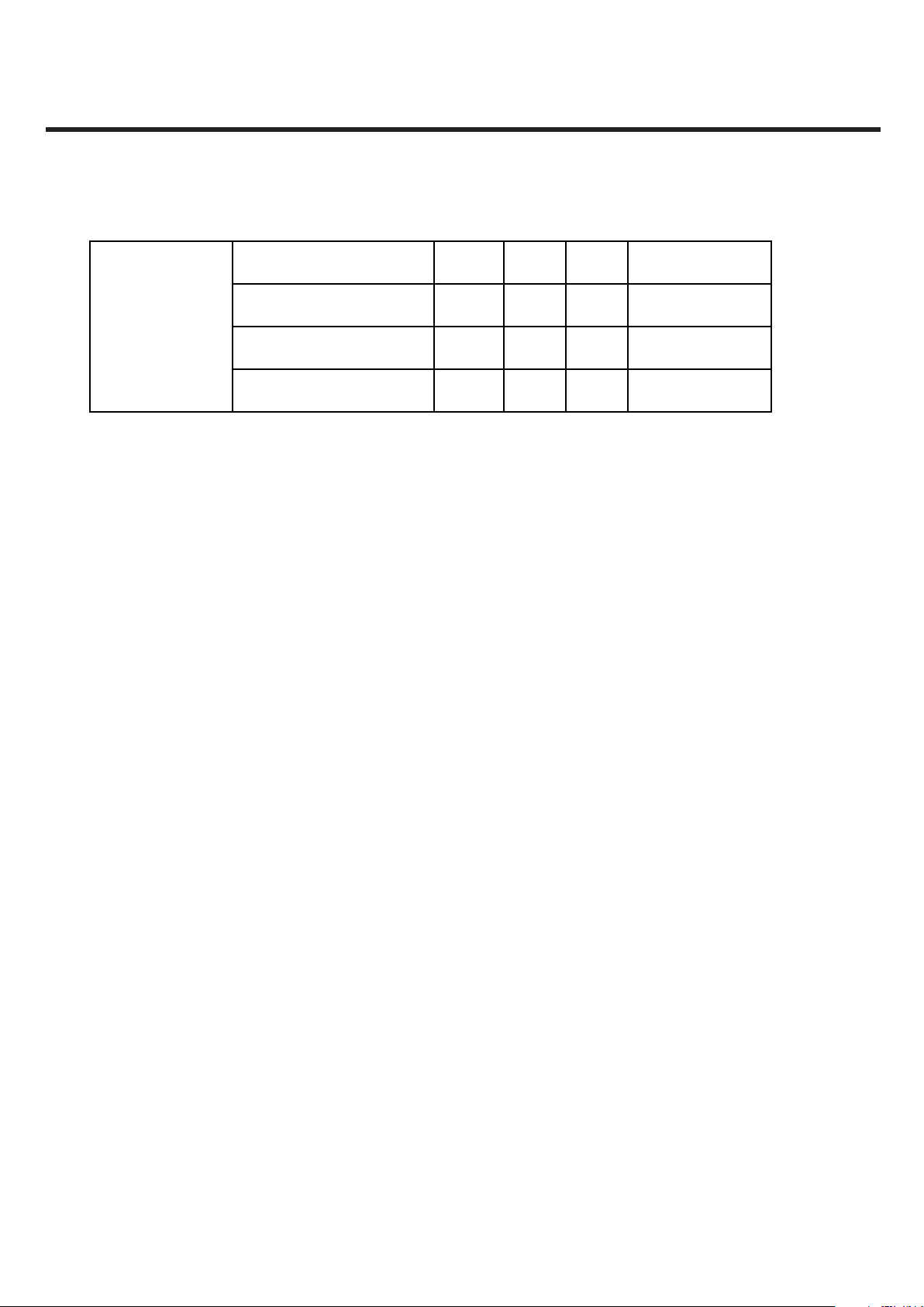
2.3 Main Parts : GSM Solution
Item Part Name Comment
AP Chip MT6577 (MTK)
CP Chip MT6577 (MTK)
LGE Internal Use Only
- 5 -
Copyright © 2013 LG Electronics. Inc. All right reserved.
Only for training and service purposes
2. PERFORMANCE
LG-D685 Product SPEC
2.4 HW Features
2.4 HW Features
List Type / Spec.
1. Phone Type DOP Type
2. Size 150.25 x 76.94 x 9.43mm
3. Weight 163.9 g
4. Battery
5.Chipset MT6577
6. Memory 8GB(EMMC) +8Gb(LPDDR2)
Brazil : 3,040mAh ( typ.)
Other Country : 3,140mAh ( typ.), 3,040mAh(min) (Li-Ion)
Size 5.5 inch
Dot 540(H) X 960(V)
7. LCD
8. Main Camera (8M)
Color 16.7M colors
Display Type Active matrix TFT, Transmissive Type
NTSC Typ. 70%
Contrast Ratio Typ. 1000:1
Pixel Pitch 0. 042mm (201.6ppi)
Color temperature 5000 ~ 9000(K) ( typ. 6500K)
Type CMOS image sensor
Resolution 3296(H) X 2512(V) pixels.
Frame Rate 22.5 fps@ Full Size(3280*2464)
View Angle 71.4˚ ± 1˚ (Diagonal)
LGE Internal Use Only
Image Scaling Down 8M(3264x2448), W6M(3264x1836),
- 6 -
Copyright © 2013 LG Electronics. Inc. All right reserved.
Only for training and service purposes
2. PERFORMANCE
LG-D685 Product SPEC
5M(2592x1944), 1M(1280x960)
10. Audio
11. Bluetooth
12. WLAN
13. GPS type A-GPS, GNSS
Pixel x size
1.1um X 1.1um (square pixel)
1) MIDI MIDI
2) Mono 15 X 11 X 3T Speaker
3) Receiver 13 X 07 X 2.7T Wideband Receiver
Effective Distance 10M
Distance 0 m ~ 10 m (depend on environment)
standard IEEE 802.11 b/g/n
Throughput Max 40Mbps (SDIO Driver performance)
depend on environment 0 ~ 50m (depend on environment)
LGE Internal Use Only
- 7 -
Copyright © 2013 LG Electronics. Inc. All right reserved.
Only for training and service purposes
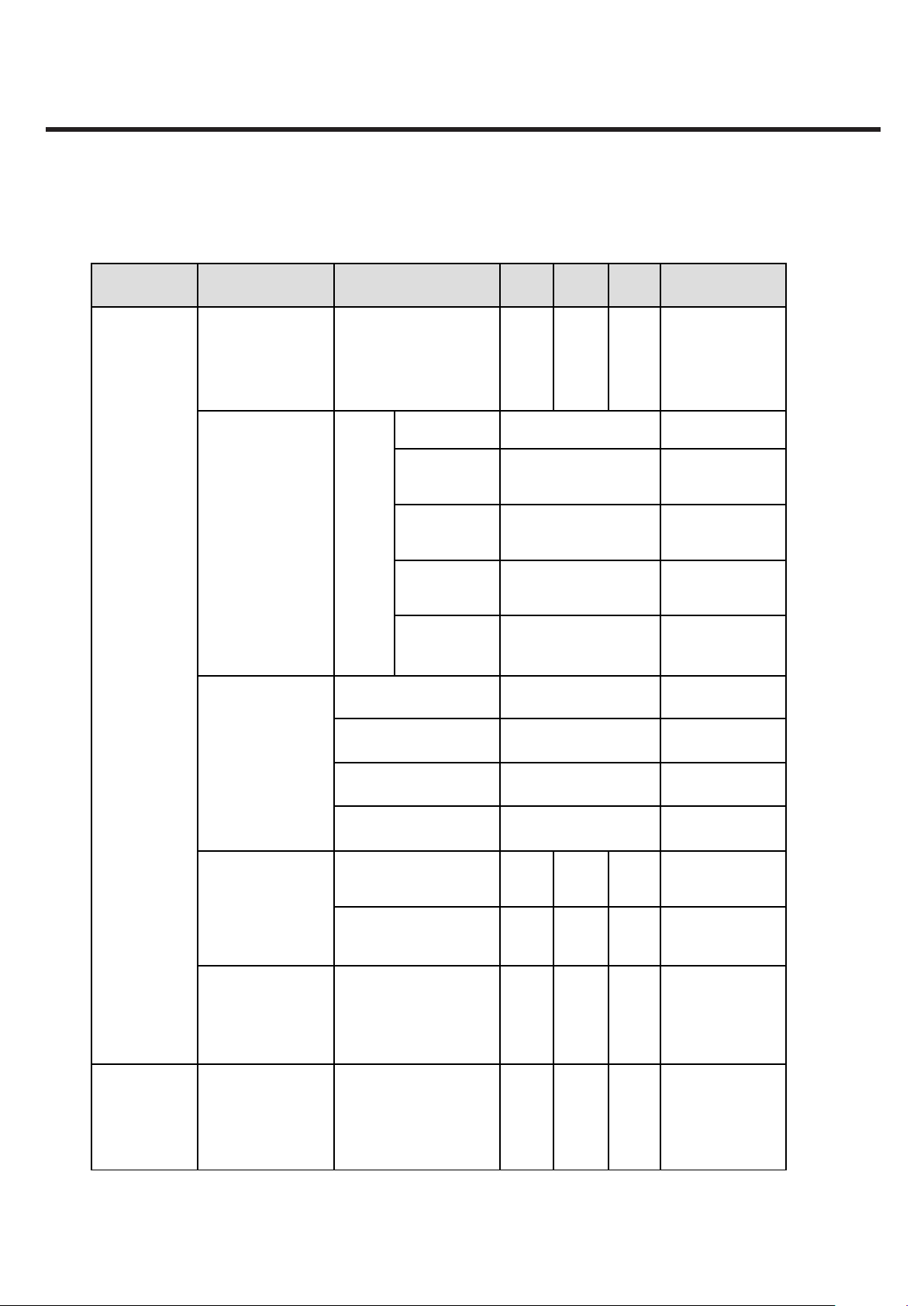
2.5 HW SPEC
LG-D685 Product SPEC
2.5. HW SPEC.
1) WCDMA transmitter specification
2. PERFORMANCE
1) WCDMA transmitter specication
Item Spec. Min Typ. Max Unit
Maximum Output
Power
Frequency
Accuracy
Minimum Output
Power
Occupied
Bandwidth
Adjacent Channel
Leakage Power
Ratio
Error Vector
Magnitude(EVM)
Power class Ⅲ 21.0 23.0 25.0
Δf = ± 5MHz
Δf = ± 10MHz
dBm/3.84MHz
- -200 - +200 Hz
- - - -50 dBm/3.84MHz
- - - 4.6 MHz
- - -33 dBm/3.84MHz
- - -43 dBm/3.84MHz
- - - 17
%
Peak Code
Domain Error
Open Loop
Output Power
Transmit Off
Power
Spectrum
Emission Mask
- - - 15
Ior =-106.7dBm/3.84MHz -46.7 - -28.7
Ior =-65.7dBm/3.84MHz -23.0 - -5.0
Ior =-25.0dBm/3.84MHz -0.0 - 14.0
- - - -56 dBm/3.84MHz
Δf = 2.5~3.5MHz -35-15 * (Δf-2.5) dBc/30KHz
Δf = 3.5~7.5MHz -35-1 * (Δf-3.5) dBc/1MHz
Δf = 7.5~8.5MHz -39 10 * (Δf-7.5) dBc/1MHz
Δf = 8.5~12.5MHz -49 dBc/1MHz
dBm/3.84MHz
dBm/3.84MHz
dBm/3.84MHz
dBm/3.84MHz
LGE Internal Use Only
- 8 -
Copyright © 2013 LG Electronics. Inc. All right reserved.
Only for training and service purposes
2. PERFORMANCE
LG-D685 Product SPEC
Transmit Spurious
Emission
9kHz ~ 150kHz
150kHz ~ 30MHz
30MHz ~ 1GHz
1GHz ~ 12.5GHz
-36
-36
-36
-30
dBm
dBm
dBm
dBm
LGE Internal Use Only
- 9 -
Copyright © 2013 LG Electronics. Inc. All right reserved.
Only for training and service purposes
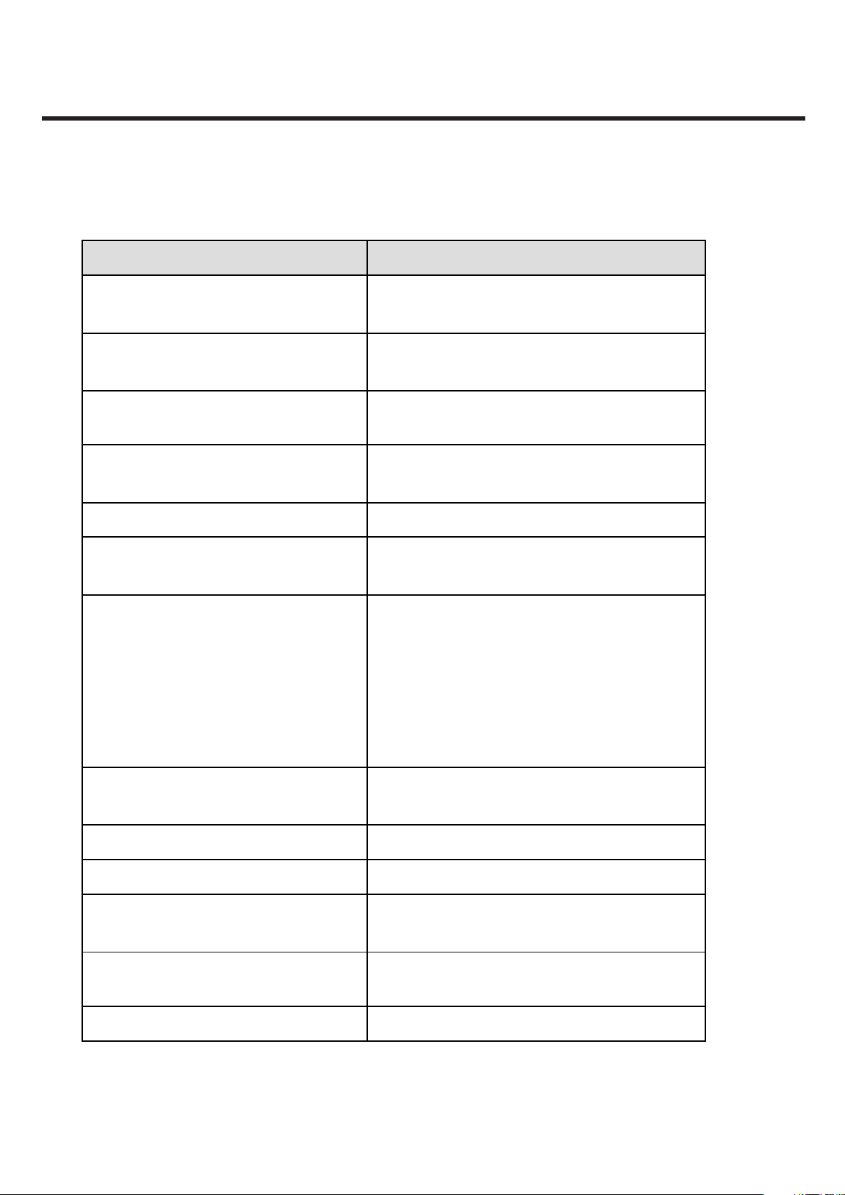
LG-D685 Product SPEC
2) WCDMA receiver specification
2) WCDMA receiver specication
Item Specification
2. PERFORMANCE
FDD1: 2110 ~ 2170 MHz
Receive Frequency
Reference Sensitivity Level
<REFÎ
>
or
Maximum Input Level BER < 0.001 when Îor = -25 dBm / 3.84 MHz
Adjacent Channel Selectivity
(ACS)
Blocking Characteristic
Spurious Response
FDD2: 1930 ~ 1990 MHz
FDD5: 869 MHz ~ 894 MHz
FDD8: 925 MHz ~ 960 MHz
FDD1 : BER < 0.001 when Îor = -106.7 dBm / 3.84 MHz
FDD2 : BER < 0.001 when Îor = -104.7 dBm / 3.84 MHz
FDD5 : BER < 0.001 when Îor = -104.7 dBm / 3.84 MHz
FDD8 : BER < 0.001 when Îor = -103.7 dBm / 3.84 MHz
ACS > 33 dB where BER < 0.001 when
Îor = <REFÎ
> + 14 dB / 3.84 MHz
or
& Ioac = –52 dBm / 3.84 MHz @ ±5 MHz
BER < 0.001 when Îor = <REFÎ
> + 3 dB / 3.84 MHz
or
& Iblocking = -56 dBm / 3.84 MHz @ Fuw(offset) = ±10 MHz
or Iblocking = -44 dBm / 3.84 MHz @ Fuw(offset) = ±15 MHz
BER < 0.001 when Îor = <REFÎ
> + 3 dB / 3.84 MHz
or
& Iblocking = -44 dBm
Intermodulation
Spurious Emissions
Inner Loop Power Control
In Uplink
LGE Internal Use Only
BER < 0.001 when Îor= <REFÎ
> + 3 dB / 3.84 MHz
or
& Iouw1 = -46 dBm @ Fuw1(offset) = ±10 MHz
& Iouw2 = -46 dBm / 3.84 MHz @ Fuw2(offset) = ±20 MHz
< -57 dBm / 100 kHz BW @ 9 kHz ≤ f < 1 GHz
< -47 dBm / 1 MHz BW @ 1 GHz ≤ f ≤ 12.75 GHz
Adjust output(TPC command)
cmd 1dB 2dB 3dB
+1 +0.5/1.5 +1/3 +1.5/4
0 -0.5/+0.5 -0.5/+0.5 -0.5/+0.5
-1 -0.5/-1.5 -1/-3 -1.5/-4
group(10equal command group)
+1 +8/+12 +16/+24
- 10 -
Copyright © 2013 LG Electronics. Inc. All right reserved.
Only for training and service purposes
LG-D685 Product SPEC
3) HSDPA transmitter specification
Input Level for
3) HSDPA transmitter specication
Item Spec. Min Typ. Max Unit
5.2.A Maximum
Output Power
with HS-DPCCH
1/15 ≤ βc/βd ≤ 12/15
13/15 ≤ βc/βd ≤ 15/8
15/7 ≤ βc/βd ≤ 15/0
2. PERFORMANCE
21.0
20
19
23.0
23.0
22.5
25.0
25
25
dBm/3.84MHz
Trandsmitter
5.7A HS-DPCCH
5.9A Spectrum
Emission Mask
with HS-DPCCH
5.10A Adjacent
Channel Leakage
Power Ratio with
HS-DPCCH
Step 0
Step 1 –
Step 0
MAX
/
0dBm
Δf = 2.5~3.5MHz -35-15 * (Δf-2.5) dBc/30KHz
Δf = 3.5~7.5MHz -35-1 * (Δf-3.5) dBc/1MHz
Δf = 7.5~8.5MHz -39 10 * (Δf-7.5) dBc/1MHz
Δf = 8.5~12.5MHz -49 dBc/1MHz
Δf = ± 10MHz
Step 2 –
Step 3
Step 5 –
Step 4
Step 6 –
Step 7
Δf = ± 5MHz
0 dBm +/- 1 dB dB
6 dB +/- 2.3 dB dB
1 dB +/- 0.6 dB dB
0 dB +/- 0.6 dB dB
5 dB +/- 2.3 dB dB
- - -33 dBm/3.84MHz
- - -43 dBm/3.84MHz
Receiver
LGE Internal Use Only
5.13.1A Error
Vector
Magnitude (EVM)
with HS-DPCCH
6.3A Maximum
HS-PDSCH
Reception
MAX Power
-20 dBm
Pin = -25dBm - - 10 BLER(%)
- 11 -
- - 17.5
Copyright © 2013 LG Electronics. Inc. All right reserved.
Only for training and service purposes
%
LG-D685 Product SPEC
4) GSM receiver specification
4) GSM receiver specication
2. PERFORMANCE
Item
EMC(Radiated Spurious Emission
Transmitter Output power and Burst Timing
Spectrum due to modulation out to less
Spectrum due to modulation out to larger
than 1800kHz offset to the edge of the
Phase Error
Frequency Error
Disturbance)
Burst Timing
than 1800kHz offset
transmit band
Spec.
Rms : 5°
Peak : 20 °
GSM : 0.1 ppm
DCS/PCS : 0.1 ppm
3000kHz-6000kHz : <-65dBc(-46dBm)
GSM/DCS : < -28dBm
GSM : 5dBm – 33dBm ± 3dB
DCS/PCS : 0dBm – 30dBm ± 3dB
<3.69us
200kHz : -36dBm
600kHz : -51dBm/-56dBm
GSM :
1800-3000kHz :< -63dBc(-46dBm)
6000kHz < : < -71dBc(-46dBm)
DCS :
1800-3000kHz :< -65dBc(-51dBm)
6000kHz < : < -73dBc(-51dBm)
Spectrum due to switching transient
Reference Sensitivity – TCH/FS
Usable receiver input level range
Intermodulation rejection – Speech
channels
AM Suppression
- GSM : -31dBm - DCS : -29dBm
Timing Advance
LGE Internal Use Only
400kHz : -19dBm/-22dBm(5/0), -23dBm
600kHz : -21dBm/-24dBm(5/0), -26dBm
Class II(RBER) : -105dBm(2.439%)
0.012(-15 - -40dBm)
± 800kHz, ± 1600kHz
: -98dBm/-96dBm (2.439%)
-98dBm/-96dBm (2.439%)
± 0.5T
- 12 -
Copyright © 2013 LG Electronics. Inc. All right reserved.
Only for training and service purposes
2. PERFORMANCE
LG-D685 Product SPEC
5) Bluetooth transmitter specification
5) Bluetooth transmitter specication
Item Spec. Min Typ. Max
Output Power
Power Density
Power Control
Frequency Range
Tx Output Spectrum
(20dB BW)
Tx Output Spectrum
(Adjacent Output
Power)
DH5
PRBS9
DH5
PRBS9
DH1
PRBS9
DH5
PRBS9
DH5
PRBS9
DH5
PRBS9
Power
(Class I)
@100kHz RBW
Step size
Power(min)
-30dBc
@100kHz RBW
Δf =f
H-fL
@M-N = 2
@M-N ≥ 3
Unit
0 - 20
- +20
dBm
dBm
2 - 8 dB
- 4 dBm
2400 - 2483.5 MHz
- 1 MHz
- -20
- -40
dBm
dBm
Modulation Index
Initial Carrier Freq.
Tolerance
Carrier Frequency Drift
DH5
11110000
DH5
10101010
DH5
PRBS9
DH1
10101010
DH3
10101010
Freq. Drift -40 - +40
DH5
10101010
Drift Rate -20 - +20
f1
AVG
f2
MAX
f2
/f1
AVG
AVG
140 - 175
115 -
0.8 -
-75 - +75
Freq. Drift -25 - +25
Drift Rate -20 - +20
Freq. Drift -40 - +40
Drift Rate -20 - +20
kHz
kHz
kHz
kHz
kHz/50us
kHz
kHz/50us
kHz
kHz/50us
LGE Internal Use Only
- 13 -
Copyright © 2013 LG Electronics. Inc. All right reserved.
Only for training and service purposes
6) Bluetooth receiver specication
Item Spec. BER=0.1% Min Typ. Max Unit
2. PERFORMANCE
Sensitivity
(Single Slot Packet)
Sensitivity
(Multi Slot Packet)
C/I Performance*
DH1
PRBS9
Input power @BT_w
DH5
PRBS9
Input power @BT_w
DH1
PRBS9
Input power @BT_i
-
-
C/I@Co-Channel
-60dBm @ BT
C/I @1MHz
-60dBm@ BT
C/I @2MHz
-60dBm@ BT
C/I @≥3MHz
-67dBm@ BT
- -70 dBm
- -70 dBm
- 11
- 0
- -30
dB
-40 -37
Blocking Performance
DH1
PRBS9
Input power @CW
C/I @Image
-67dBm@ BT
C/I @ Image±1MHz
-67dBm@ BT
30M ~2 GHz
-67dBm@ BT
2 ~ 2.4 GHz
-67dBm@ BT
2.5 ~ 3 GHz
-67dBm@ BT
3 ~ 12.75 GHz
-67dBm@ BT
-10 -
-27 -
-27 -
-10 -
- -9
- -20
dBm
LGE Internal Use Only
- 14 -
Copyright © 2013 LG Electronics. Inc. All right reserved.
Only for training and service purposes
Δf = +5MHz (CW_i)
2. PERFORMANCE
Intermodulation
Performance
Maximum Input Level
DH1
PRBS9
Input power @CW_i
DH1
PRBS9
Input power @BT_w
Δf = +10MHz (BT_i)
-64dBm@ BT_w
Δf = -5MHz (CW_i)
Δf = -10MHz (BT_i)
-64dBm@ BT_w
- -20 -
-39 -
-39 -
dBm
dBm
dBm
LGE Internal Use Only
- 15 -
Copyright © 2013 LG Electronics. Inc. All right reserved.
Only for training and service purposes
LG-D685 Product SPEC
7) WLAN 802.11b transceiver specification
7) WLAN 802.11b transceiver specication
Item Specification
Transmit Frequency 2400 MHz ~ 2483.5 MHz ( CH1~CH13)
2. PERFORMANCE
Tx Power Level
Frequency Tolerance within ±25 PPM
Chip clock Frequency
Tolerance
≤ -30 @ fc-22MHz< f <fc-11MHz and fc+11MHz< f <fc+22MHz
Spectrum Mask
Power ramp on/off time
Carrier Suppression
Modulation Accuracy
(Peak EVM)
≤ 20dBm under (Europe), ≤ 30dBm under (USA)
within ±25 PPM
≤ -50 @ f < fc-22MHz and f > fc+22MHz
≤ 2us
≤ -15dB
≤ 35%
< -36 dBm @ 30MHz ~ 1GHz
Spurious Emissions
Rx Min input Sensitivity
Rx Max input Sensitivity
Rx Adjacent Channel
Rejection
LGE Internal Use Only
< -30 dBm above @ 1GHz ~ 12.75GHz
< -47 dBm @ 1.8GHz ~ 1.9GHz
< -47 dBm @ 5.15GHz ~ 5.3GHz
≤ -76dBm(1Mbps,2Mbps,5.5Mbps,11Mbps) @ FER ≤ 8%
≥ -10dBm(1Mbps,2Mbps,5.5Mbps,11Mbps) @ FER ≤ 8%
≥ 35dB @FER ≤ 8%,
interference input signal -70dBm@fc±25MHz(11Mbps)
- 16 -
Copyright © 2013 LG Electronics. Inc. All right reserved.
Only for training and service purposes
2. PERFORMANCE
LG-D685 Product SPEC
8) WLAN 802.11g transceiver specification
8) WLAN 802.11g transceiver specication
Item Specification
Transmit Frequency
Tx Power Level
Frequency Tolerance within ±25 PPM
Chip clock Frequency
Tolerance
Spectrum Mask
Transmitter constellation error
(rms EVM)
2400 MHz ~ 2483.5 MHz ( CH1~CH13)
≤ 20dBm under (Europe), ≤ 30dBm under (USA)
within ±25 PPM
≤ -20 @ ±11MHz offset (9Mhz ~ 11MHz)
≤ -28 @ ±20MHz offset (11MHz ~ 20Mhz)
≤ -40 @ ±30MHz offset (20MHz ~ 30Mhz)
≤ -5dB
Spurious Emissions
Rx Min input Sensitivity
Rx Max input Sensitivity
Rx Adjacent Channel
Rejection
< -36 dBm @ 30MHz ~ 1GHz
< -30 dBm above @ 1GHz ~ 12.75GHz
< -47 dBm @ 1.8GHz ~ 1.9GHz
< -47 dBm @ 5.15GHz ~ 5.3GHz
PER ≤ 10%
-82dBm@6Mbps, -81dBm@9Mbps, -79dBm@12Mbps
-77dBm@18Mbps, -74dBm@24Mbps, -70dBm@36Mbps
-66dBm@48Mbps, -65dBm@54Mbps
≥ -20dBm(6,9,12,18,24,36,48,54Mbps) @ PER ≤ 10%
PER ≤ 10%,
ACR ≥ 16dB@6Mbps, ACR ≥ 15dB@9Mbps,
ACR ≥ 13dB@12Mbps, ACR ≥ 11dB@18Mbps,
ACR ≥ 8dB@24Mbps, ACR ≥ 4dB@36Mbps
ACR ≥ 0dB@48Mbps, ACR ≥ -1dB@54Mbps
※ACR shall be measured by setting the desired signal's strength 3 dB
LGE Internal Use Only
above the rate-dependent
sensitivity specified in min input sensitivity
- 17 -
Copyright © 2013 LG Electronics. Inc. All right reserved.
Only for training and service purposes
2. PERFORMANCE
LG-D685 Product SPEC
9) WLAN 802.11n transceiver specification
9) WLAN 802.11n transceiver specication
Item Specification
Transmit Frequency
Tx Power Level ≤ 20dBm under (Europe), ≤ 30dBm under (USA)
Frequency Tolerance within ±25 PPM
Chip clock Frequency
Tolerance
Spectrum Mask
Transmitter constellation error
(rms EVM)
2400 MHz ~ 2483.5 MHz ( CH1~CH13)
within ±25 PPM
≤ -20 @ ±11MHz offset (9Mhz ~ 11MHz)
≤ -28 @ ±20MHz offset (11MHz ~ 20Mhz)
≤ -45 @ ±30MHz offset (20MHz ~ 30Mhz)
≤ -5dB@6.5Mbps, ≤ -10dB@13Mbps, ≤ -13dB@19.5Mbps,
≤ -16dB@26Mbps, ≤ -19dB@39Mbps, ≤ -22dB@52Mbps,
≤ -25dB@58.5Mbps, ≤ -28dB@65Mbps
< -36 dBm @ 30MHz ~ 1GHz
Spurious Emissions
-82dBm@6.5Mbps, -79dBm@13Mbps, -77dBm@19.5Mbps
Rx Min input Sensitivity
-74dBm@26Mbps, -70dBm@39Mbps, -66dBm@52Mbps
Rx Max input Sensitivity ≥ -20dBm(6.5,13,19.5,26,39,52,58.5,65Mbps) @ PER ≤ 10%
Rx Adjacent Channel
Rejection
※ACR shall be measured by setting the desired signal's strength
< -30 dBm above @ 1GHz ~ 12.75GHz
< -47 dBm @ 1.8GHz ~ 1.9GHz
< -47 dBm @ 5.15GHz ~ 5.3GHz
PER ≤ 10%
-65dBm@58.5Mbps, -64dBm@65Mbps
PER ≤ 10%,
ACR ≥ 16dB@6.5Mbps, ACR ≥ 13dB@13Mbps,
ACR ≥ 11dB@19.5Mbps, ACR ≥ 8dB@26Mbps,
ACR ≥ 4dB@39Mbps, ACR ≥ 0dB@52Mbps
ACR ≥ -1dB@58.5Mbps, ACR ≥ -2dB@65Mbps
LGE Internal Use Only
3 dB above the rate-dependent
sensitivity specified in min input sensitivity
- 18 -
Copyright © 2013 LG Electronics. Inc. All right reserved.
Only for training and service purposes
10) GPS receiver specication
LG-D685 Product SPEC
10) GPS receiver specification
LG-D685 Product SPEC
10) GPS receiver specification
Item Spec.
Sensitivity Test
Success rate ≥ 60% @ -154 dBm
11) Current consumption
** Test condition for Standby current consumption should be as below.
: Measurement time 1hr, with Agilent & CMT JIG
-
Item Spec.
2. PERFORMANCE
Sensitivity Test
11) Current consumption
** Test condition for Standby current consumption should be as below.
: Measurement time 1hr, with Agilent & CMT JIG
Item
1. Sleep Mode
2. Sleep : connector Ear jack
3. Current(Sleep & Idle AVG) Under 10mA @ DRX 7 Under 10mA @ P.P 5
4. BT Connected idle
WCDMA
Under 7mA
Under 7mA
Under 15mA
Success rate ≥ 60% @ -154 dBm
Specification
GSM
Under 7mA
Under 7mA
Under 15mA
5. Talk Mode
6. Power Off Mode
7. Backup Battery
LGE Internal Use Only
Max Pwr
Under 600mA @ Avg
- Tx 10dBm
Under 300 mA @ Avg
under 500uA
under 5uA
- 19 -
Copyright © 2013 LG Electronics. Inc. All right reserved.
GSM LVL 5
under 300 mA @ Avg
Under 500 uA
under 5uA
Only for training and service purposes
LG-D685 Product SPEC
12) RSSI indicator (Based on Cell power)
LG-D685 Product SPEC
12) RSSI indicator (Based on Cell power)
BAR
WCDMA
GSM/DCS/PCS
RSSI RSCP
5
Over -85 ±2dBm
Over -88 ±2dBm
Over -91 ±2dBm
54
-86 ±2dBm
-89 ±2dBm
-92 ±2dBm
43
-90 ±2dBm
-93 ±2dBm
-96 ±2dBm
32
-96 ±2dBm
-99 ±2dBm
-100 ±2dBm
21
-100 ±2dBm
-103 ±2dBm
-104 ±2dBm
10
-107 ±3dBm
-109 ±3dBm
-106 ±3dBm
13) Current consumption
Standby
(WCDMA)
Over 350 Hours
Under 4.5mA
DRX 7 @ BATT Capacity : 3140mAh
14) Charging hour
Under 4 hour (3140mAh battery, 1.2A TA)
12) RSSI indicator (Based on Cell power)
BAR
2. PERFORMANCE
WCDMA
GSM/DCS/PCS
RSSI RSCP
13) Current consumption
14) Charging hour
Under 4 hour (3140mAh battery, 1.2A TA)
5
54
43
32
21
10
Standby
(WCDMA)
Over -85 ±2dBm
-86 ±2dBm
-90 ±2dBm
-96 ±2dBm
-100 ±2dBm
-107 ±3dBm
Over 350 Hours
Under 4.5mA
Over -88 ±2dBm
-89 ±2dBm
-93 ±2dBm
-99 ±2dBm
-103 ±2dBm
-109 ±3dBm
DRX 7 @ BATT Capacity : 3140mAh
Over -91 ±2dBm
-92 ±2dBm
-96 ±2dBm
-100 ±2dBm
-104 ±2dBm
-106 ±3dBm
LGE Internal Use Only
- 20 -
Copyright © 2013 LG Electronics. Inc. All right reserved.
Only for training and service purposes

LG-D685 Product SPEC
15) Battery indicator
15) Battery indicator
Battery Bar Specification
BAR 20 (Full) 98% over
2. PERFORMANCE
BAR 20 --> 19
BAR 19 --> 18
BAR 18 --> 17
BAR 17 --> 16
BAR 16 --> 15
BAR 15 --> 14
BAR 14 --> 13
BAR 13 --> 12
BAR 12 --> 11
BAR 11 --> 10
BAR 10 --> 9
BAR 9 --> 8
BAR 8 --> 7
BAR 7 --> 6
BAR 6 --> 5
98% ◊ 97%
93% ◊ 92%
88% ◊ 87%
83% ◊ 82%
78% ◊ 77%
73% ◊ 72%
68% ◊ 67%
63% ◊ 62%
58% ◊ 57%
53% ◊ 52%
48% ◊ 47%
43% ◊ 42%
38% ◊ 37%
33% ◊ 32%
28% ◊ 27%
remain%
LGE Internal Use Only
BAR 5 --> 4
BAR 4 --> 3
BAR 3 --> 2
BAR 2 --> 1
BAR 1 --> 0
Low Battery Pop-up 4% ~ 15% : One Time popup (No call)
Critical Low Battery Pop-up 0% ~ 3% : Every Level change popup (No call)
Power Off 1%
- 21 -
23% ◊ 22%
16% ◊ 15%
13% ◊ 12%
8% ◊ 7%
3% ◊ 2%
Copyright © 2013 LG Electronics. Inc. All right reserved.
Only for training and service purposes
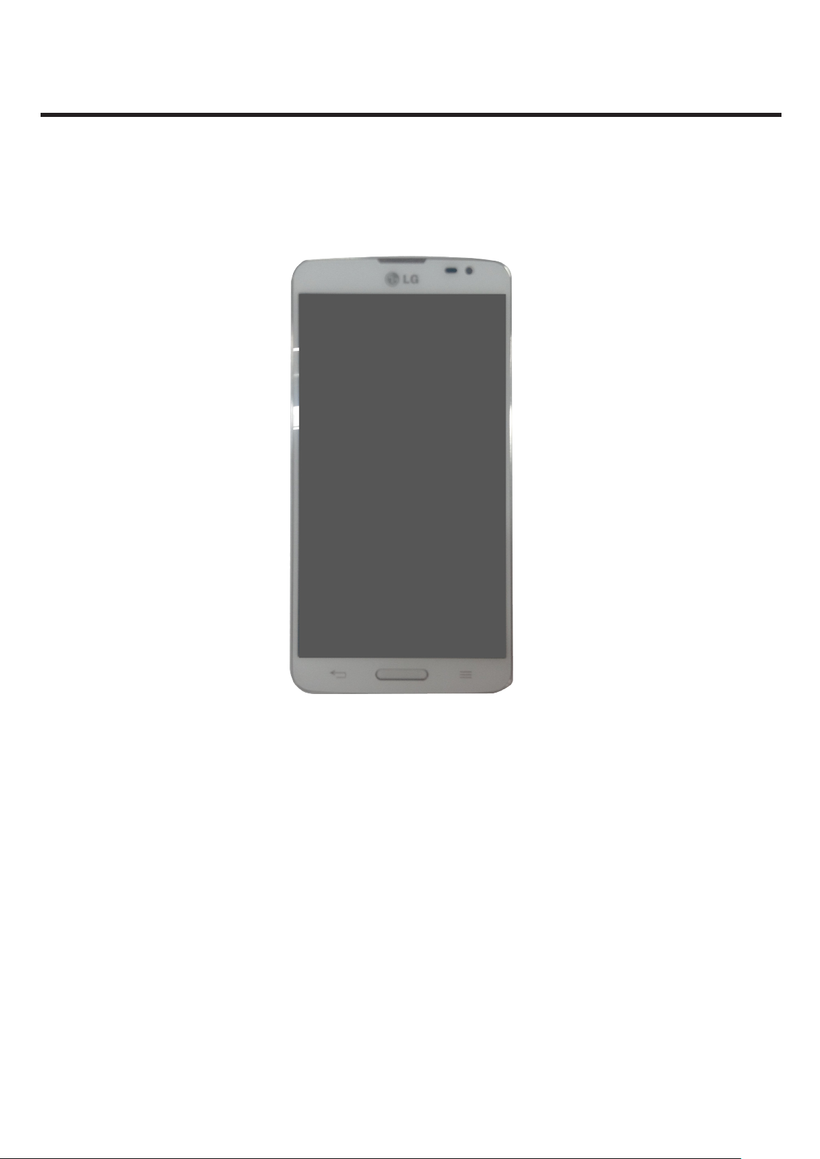
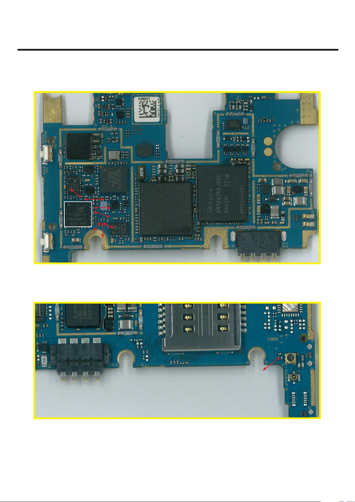
2.6 D682 Figures
2. PERFORMANCE
LGE Internal Use Only
- 22 -
Copyright © 2013 LG Electronics. Inc. All right reserved.
Only for training and service purposes
3. TROUBLE SHOOTING
3.1 WCDMA Rx Part
3.1.1 WCDMA_B1/B2/B5/B8 Rx
Rx TEST SETUP
- DL Channel : 10700 / 9800/ 44407 / 3013
- Sector Power(dBm) : -23 /-23 /-23.5 / -23.5
3. TROUBLE SHOOTING
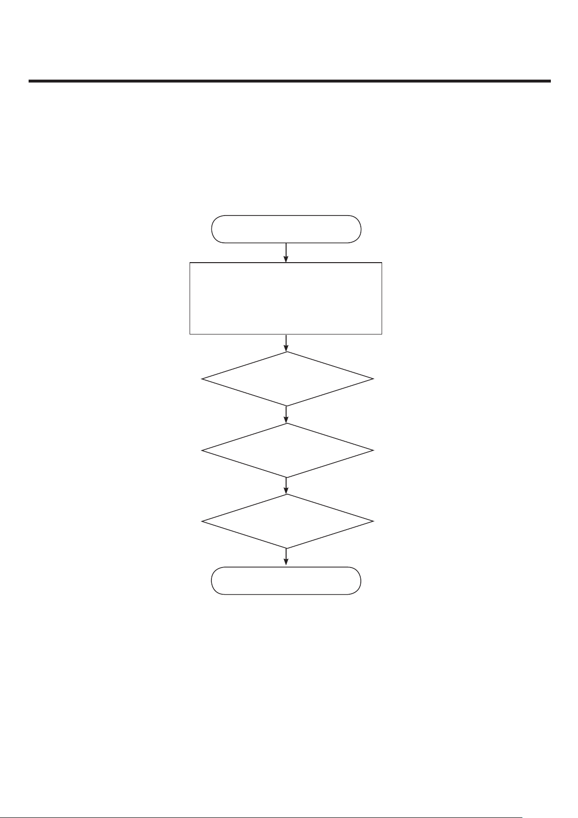
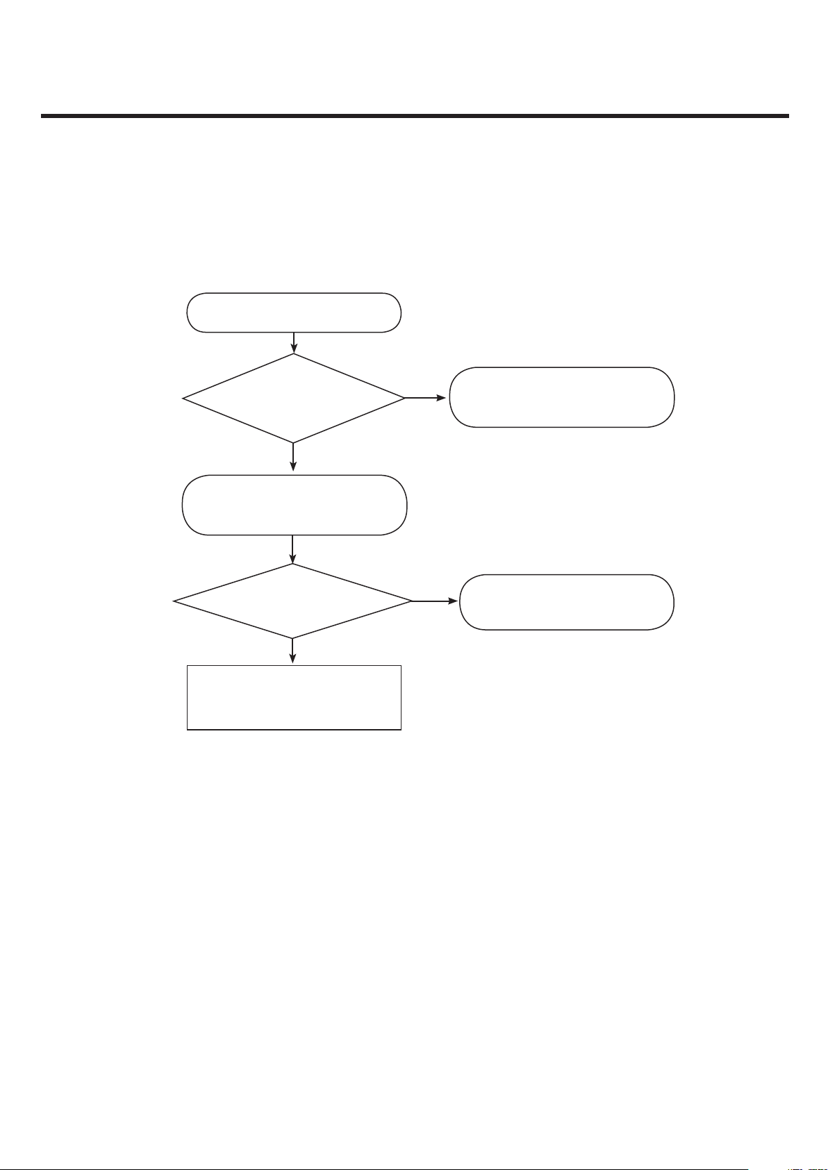
START
1. Check
DC Power Supply circuit
2. Check MT6162 XO
3.Check RF Signal path
Re download S/W & Cal
* There are no Test Points on the IQ Data Line. So It is impossible to check the IQ Data Wave form.
LGE Internal Use Only
- 23 -
Copyright © 2013 LG Electronics. Inc. All right reserved.
Only for training and service purposes
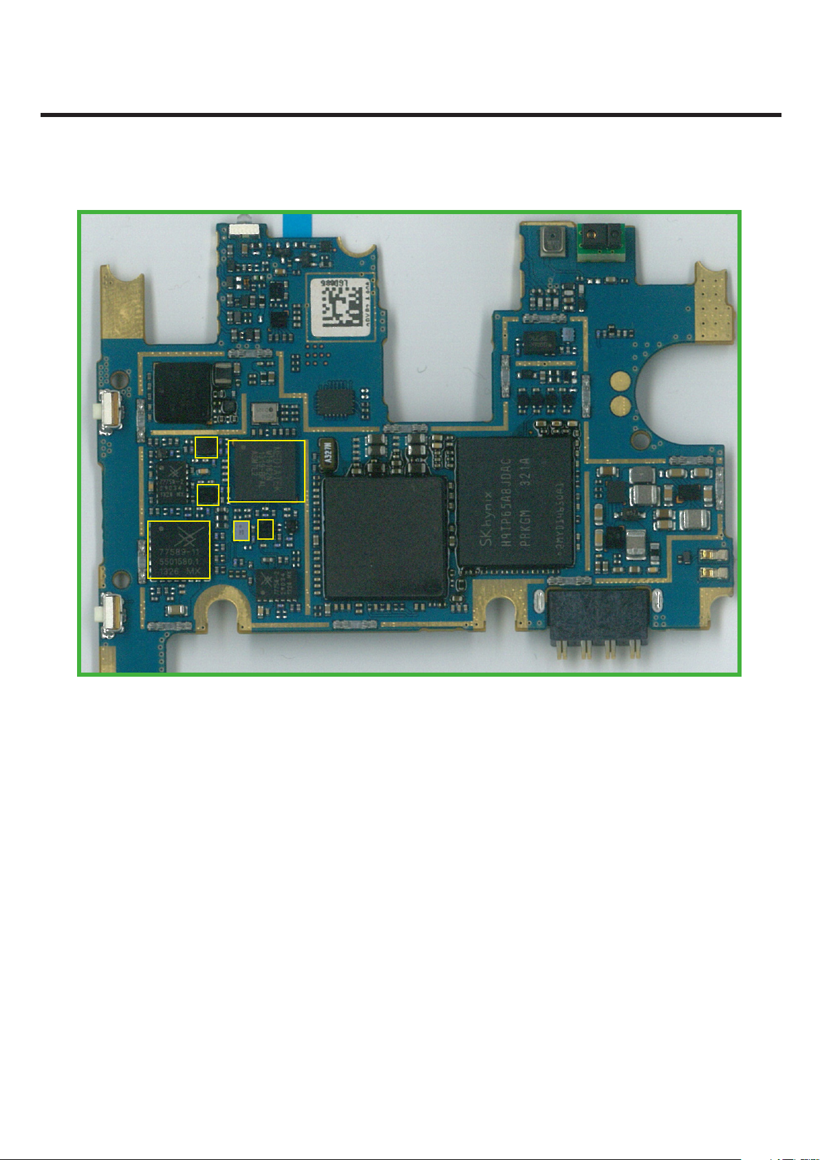
DPX
B5 (FL103)
DPX
B1 (FL105)
SKY77589
(U102)
MT6162
(U101)
DPX
(FL106) B8
3. TROUBLE SHOOTING
DPX
(FL102) B2
TOP Side
LGE Internal Use Only
- 24 -
Copyright © 2013 LG Electronics. Inc. All right reserved.
Only for training and service purposes
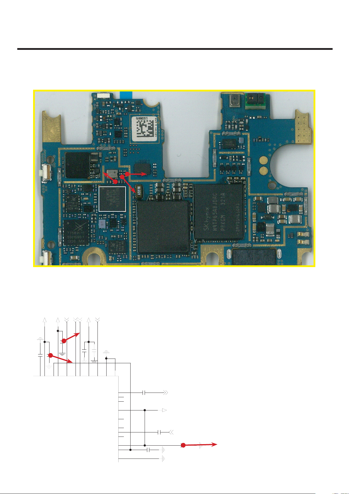
3.1.1.1 Checking DC Power supply circuit
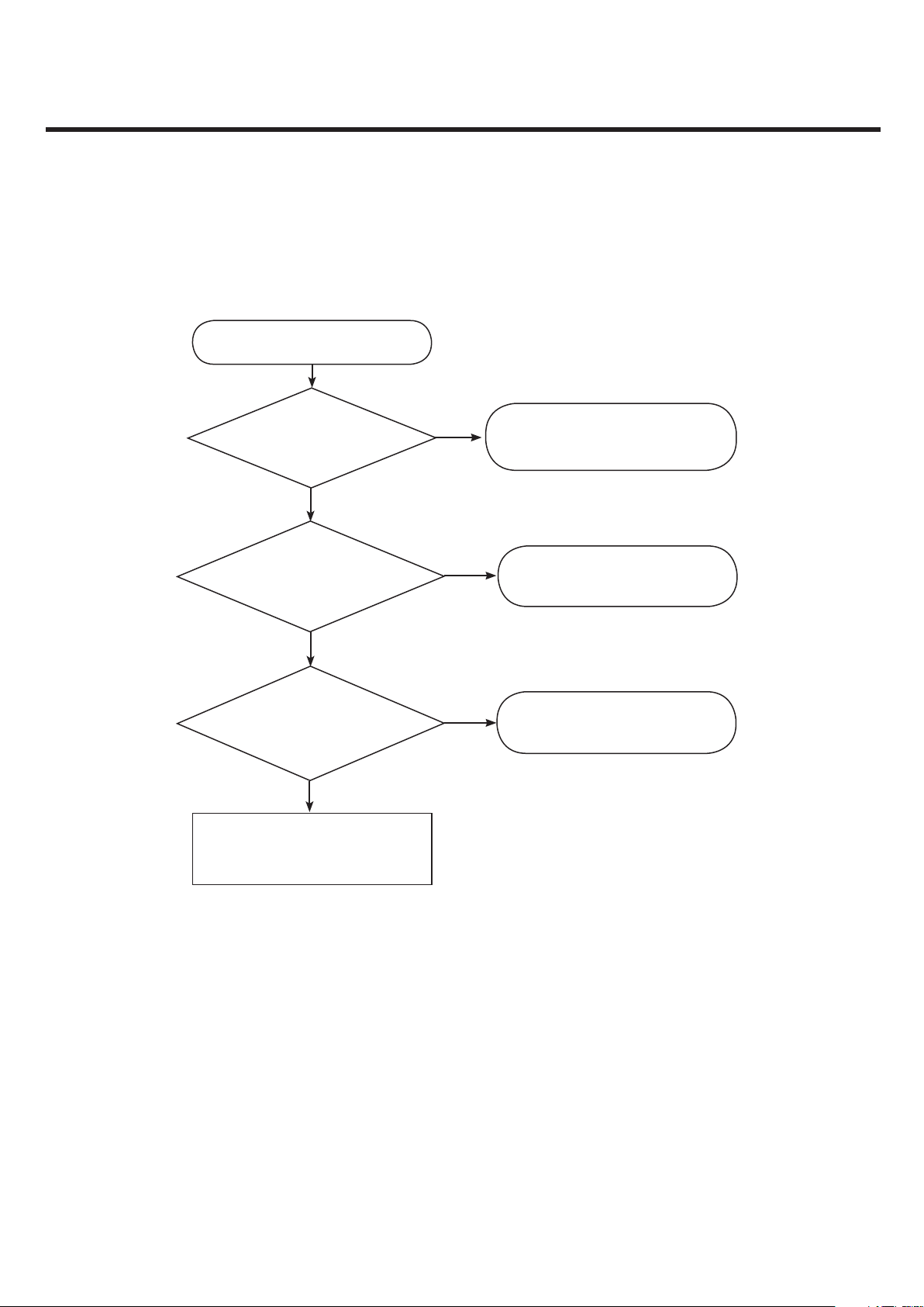
START
3. TROUBLE SHOOTING
Check TP1(C109)
+1V8_VRF_MTK is OK?
Yes
Check TP2(C103)
+2V85_VRF_MTK is OK?
Yes
Check TP3(C118)
+2V8_VTCXO_MTK is OK?
Yes
DC Power Supply Circuit is OK
See Next page to Check XO Circuit
No
No
No
The Problem may be Logic part
Refer to Logic troubleshoot
The Problem may be Logic part
Refer to Logic troubleshoot
The Problem may be Logic part
Refer to Logic troubleshoot
LGE Internal Use Only
- 25 -
Copyright © 2013 LG Electronics. Inc. All right reserved.
Only for training and service purposes
TP3: C118
(+2V8_VTCXO_MTK )
3. TROUBLE SHOOTING
TP2: C103
(+2V85_VRF_MTK )
2
1u C108
1
L2
VSUP1
+1V8_VRF_MTK
C1091u
K1
VDD_18
2
1
J2
U101
+2V85_VRF_MTK
H1
VSUP2a
VDD_28b
2
C1031u
1
G2
BSI1_CLK
BSI1_DATA
TP1
E2
F1
CLK
DATA0
BSI1_CS1
TP2
2
C1051u
1
DATA1
+1V8_VIO_MTK
D1
VINT
MT6162
(U101)
BSI1_CS0
2
C10639p
1
C2
EN
REFCLK1
REFCLK2
REFCLK3
XO1/REFIN
CLK_MODE
B1
GND2
VDDXO
NC4
XO2
VTUNE
VSUP2b
GND1
TP1 : C109
(+1V8_VRF_MTK )
1
PGND
A2
B3
A4
B5
A6
B7
A8
B9
A10
B11
A12
C112 1n
C119 1u
C114
TOP Side
SYSCLK
+2V8_VTCXO_MTK
1n
MAIN_CLK_26MHz
C118
0.1u
TP3
LGE Internal Use Only
- 26 -
Copyright © 2013 LG Electronics. Inc. All right reserved.
Only for training and service purposes
3.1.1.2 Checking MT6162 XO circuit
START
3. TROUBLE SHOOTING
Check TP1(C114)
Is it 26MHz?
NO
Replace U801 and then
check TP1(C122)
Is it similar ?
NO
Replace Main B/D
YES
YES
XO circuit is Ok . See next page
to check RF signal path.
XO circuit is Ok . See next page
to check RF signal path.
LGE Internal Use Only
- 27 -
Copyright © 2013 LG Electronics. Inc. All right reserved.
Only for training and service purposes
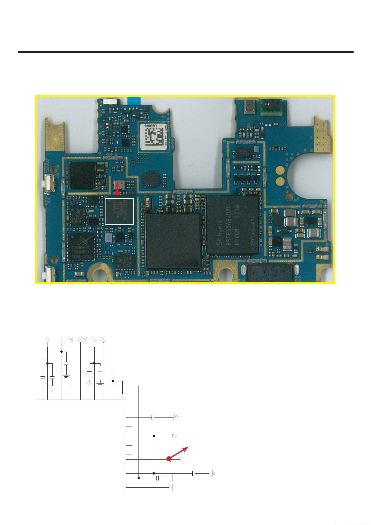
TP1 : C114
(MAIN_CLK_26MHz)
MT6162
(U101)
3. TROUBLE SHOOTING
2
1u C108
1
L2
VSUP1
+1V8_VRF_MTK
C1091u
K1
VDD_18
2
1
J2
U101
+2V85_VRF_MTK
H1
VSUP2a
VDD_28b
2
C1031u
1
G2
BSI1_CLK
BSI1_DATA
E2
F1
CLK
DATA0
TOP Side
BSI1_CS0
+1V8_VIO_MTK
BSI1_CS1
2
2
C1051u
C10639p
1
1
1
B1
C2
D1
EN
VINT
DATA1
GND2
REFCLK1
REFCLK2
REFCLK3
VDDXO
NC4
XO2
XO1/REFIN
VTUNE
CLK_MODE
VSUP2b
GND1
PGND
A2
B3
A4
B5
A6
B7
A8
B9
A10
B11
A12
C112 1n
C119 1u
C114
SYSCLK
+2V8_VTCXO_MTK
TP1
1n
MAIN_CLK_26MHz
C118
0.1u
LGE Internal Use Only
- 28 -
Copyright © 2013 LG Electronics. Inc. All right reserved.
Only for training and service purposes
3.1.1.3 Checking RF signal path(PAM)
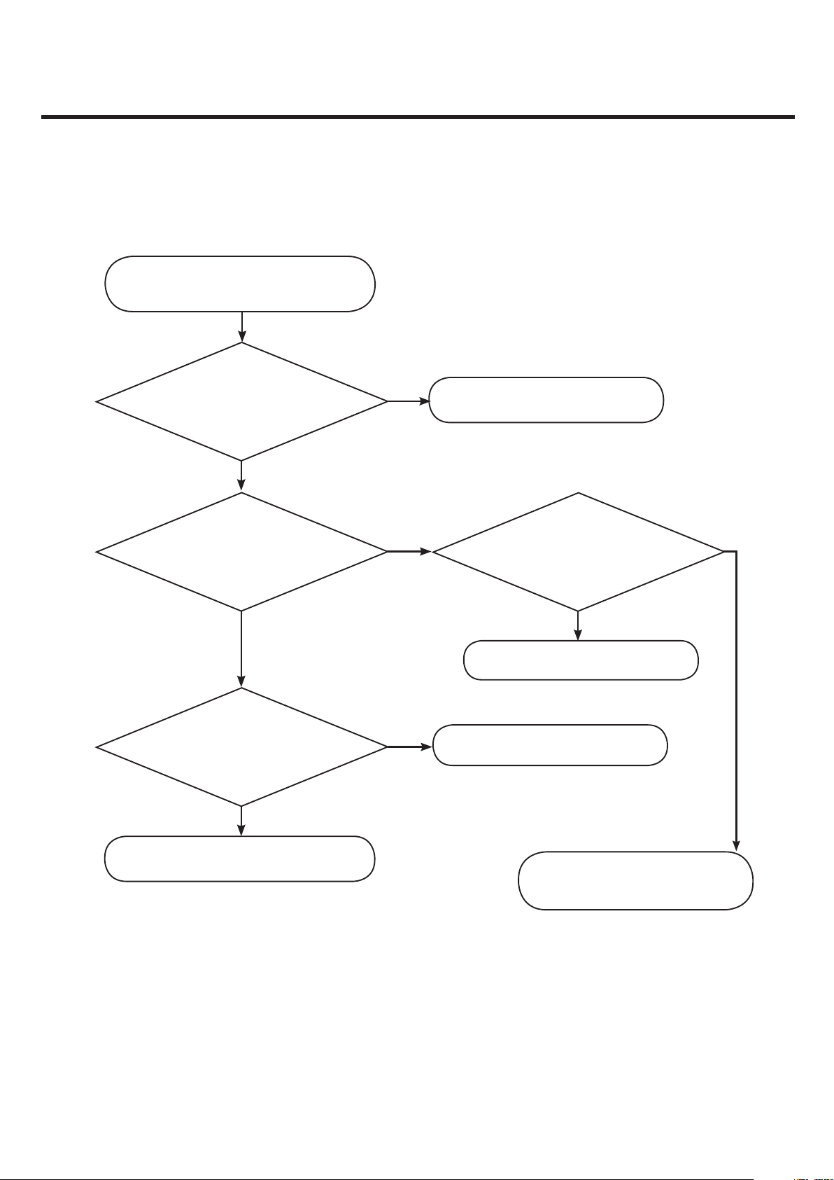
START
3. TROUBLE SHOOTING
Check TP1(L104) at U102
Check if there is any major dierence referring
To Figure 3.1.1(b). Is any signal detected at that
point?
Yes
Check TP2 at U102
Check if there is any major dierence referring
To Figure 3.1.1(c). Is any signal detected at that
point?
Yes
Is any signal detected at
that point?
No
No
No
Check anything
Check TP3(R103),TP4(R104),TP5(R105),
at U102. Is any DC signal detected
at that points?
Yes
Replace U102
Check anything
No
PAM is OK. See next page to check DPX
LGE Internal Use Only
Yes
The Problem may be Logic part
Refer to Logic troubleshoot
- 29 -
Copyright © 2013 LG Electronics. Inc. All right reserved.
Only for training and service purposes
TP2(B5): C115
SKY77589
(U102)
3. TROUBLE SHOOTING
TP2(B1): C163
TP2(B8): C117
TP2(B2): C113
TP3:R103
TP5:R105
TP4:R104
TOP Side
TP1:L104
LGE Internal Use Only
BOT Side
- 30 -
Copyright © 2013 LG Electronics. Inc. All right reserved.
Only for training and service purposes
 Loading...