

Page 1

Internal Use Only
Service Manual
LG-D405
Date: March, 2014 / Issue 0.9
Page 2

Table Of Contents
1. INTRODUCTION ..................................................................... 3
1.1 Purpose ........................................................................................................3
1.2 Regulatory Information .........................................................................3
2. PERFORMANCE ...................................................................... 5
2.1 Product Name ............................................................................................5
2.2 Supporting Standard ..............................................................................5
2.3 Main Parts : GSM Solution .....................................................................5
2.4 HW Features ...............................................................................................6
2.5 SW Features ................................................................................................9
2.6 HW SPEC. ................................................................................................. 12
3. TROUBLE SHOOTING .......................................................... 21
3.1 RF Component .......................................................................................21
3.2 SIGNAL PATH ........................................................................................... 23
3.3 Checking XO Block ................................................................................ 26
3.4 Checking FEMID (GSM, W B1/B2/B8) Block ................................. 28
3.5 Checking WCDMA Block ....................................................................31
3.6 Checking GSM Block ............................................................................ 58
3.7 GPS Trouble Shooting ......................................................................... 65
3.8 WIFI/BT Trouble Shooting .................................................................. 70
3.9 Audio Trouble ......................................................................................... 75
3.10 Camera ....................................................................................................88
3.11 Main LCD Trouble Shooting ...........................................................93
3.12 Touch troubleshooting .....................................................................96
3.13 Vibrator Trouble Shooting ...............................................................99
3.14 Gyro/Accel Trouble Shooting .......................................................101
3.15 Compass sensor troubleshooting ..............................................103
3.16 Proximity Sensor troubleshooting.............................................105
3.17 Power ON Troubleshooting ..........................................................107
3.18 FM Trouble Shooting .......................................................................111
3.19 USB Trouble Shooting ....................................................................116
4. DOWNLOAD .......................................................................120
5. BLOCK DIAGRAM ...............................................................137
6. CIRCUIT DIAGRAM ............................................................146
7. BGA PIN MAP ....................................................................162
8. PCB LAYOUT .......................................................................169
9. CALIBRATION .....................................................................173
10. HIDDEN MENU .................................................................192
11. DISASSEMBLE GUIDE ......................................................199
12. EXPLODED VIEW & REPLACEMENT PART LIST .............204
LGE Internal Use Only
- 2 -
Copyright © 2014 LG Electronics. Inc. All right reserved.
Only for training and service purposes
Page 3

1.1 Purpose
1. INTRODUCTION
This manual provides the information necessary to repair, calibration, description and download the features of
this model.
1.2 Regulatory Information
A. Security
Toll fraud, the unauthorized use of telecommunications system by an unauthorized part (for example, persons
other than your company’s employees, agents, subcontractors, or person working on your company’s behalf)
can result in substantial additional charges for your telecommunications services.
1. INTRODUCTION
System users are responsible for the security of own system. There are may be risks of toll fraud associated with
your telecommunications system. System users are responsible for programming and configuring the
equipment to prevent unauthorized use. The manufacturer does not warrant that this product is immune from
the above case but will prevent unauthorized use of common carrier telecommunication service of facilities
accessed through or connected to it. The manufacturer will not be responsible for any charges that result from
such unauthorized use.
B. Incidence of Harm
If a telephone company determines that the equipment provided to customer is faulty and possibly causing
harm or interruption in service to the telephone network, it should disconnect telephone service until repair can
be done. A telephone company may temporarily disconnect service as long as repair is not done.
C. Changes in Service
A local telephone company may make changes in its communications facilities or procedure. If these changes
could reasonably be expected to affect the use of the phones or compatibility with the net work, the telephone
company is required to give advanced written notice to the user, allowing the user to take appropriate steps to
maintain telephone service.
D. Maintenance Limitations
Maintenance limitations on the phones must be performed only by the manufacturer or its authorized agent.
The user may not make any changes and/or repairs expect as specifically noted in this manual. Therefore, note
that unauthorized alternations or repair may affect the regulatory status of the system and may void any
remaining warranty.
LGE Internal Use Only
- 3 -
Copyright © 2014 LG Electronics. Inc. All right reserved.
Only for training and service purposes
Page 4

1. INTRODUCTION
E. Notice of Radiated Emissions
This model complies with rules regarding radiation and radio frequency emission as defined by local regulatory
agencies. In accordance with these agencies, you may be required to provide information such as the following
to the end user.
F. Pictures
The pictures in this manual are for illustrative purposes only; your actual hardware may look slightly different.
G. Interference and Attenuation
A phone may interfere with sensitive laboratory equipment, medical equipment, etc. Interference from
unsuppressed engines or electric motors may cause problems.
H. Electrostatic Sensitive Devices
ATTENTION
Boards, which contain Electrostatic Sensitive Device (ESD), are indicated by the sign.
Following information is ESD handling:
• Service personnel should ground themselves by using a wrist strap when exchange system boards. • When
repairs are made to a system board, they should spread the floor with anti-static mat which is also grounded.
• Use a suitable, grounded soldering iron. • Keep sensitive parts in these protective packages until these are used.
• When returning system boards or parts like EEPROM to the factory, use the protective package as described.
LGE Internal Use Only
- 4 -
Copyright © 2014 LG Electronics. Inc. All right reserved.
Only for training and service purposes
Page 5

2. PERFORMANCE
2.1 Product Name
LG- D410 : WCDMA900/1900/2100+EGSM/GSM850/DCS1800/PCS1900(HSPA + / GPRS Class 12 / EDGE Class 12)
2.2 Supporting Standard
2.1 Product Name
LG- D410 : WCDMA900/1900/2100+EGSM/GSM850/DCS1800/PCS1900(HSPA + / GPRS Class 12 / EDGE Class 12)
2.2 Supporting Standard
Item Feature Comment
Supporting Standard WCDMA(FDD1,2,8)/
EGSM/GSM850/DCS1800/PCS1900
Frequency Range WCDMA(FDD1) TX: 1920 – 1980 MHz
WCDMA(FDD1) RX: 2110 – 2170 MHz
WCDMA(FDD2) TX: 1850– 1910 MHz
WCDMA(FDD2) RX: 1930 – 1990 MHz
WCDMA(FDD8) TX: 880–915 MHz
WCDMA(FDD8) RX: 925 – 960 MHz
EGSM TX : 880 – 915 MHz
EGSM RX : 925 – 960 MHz
GSM850 TX : 824 – 849 MHz
GSM850 RX : 869 – 894 MHz
DCS1800 TX : 1710 – 1785 MHz
DCS1800 RX : 1805 – 1880 MHz
PCS1900 TX : 1850 – 1910 MHz
PCS1900 RX : 1930 – 1990 MHz
Application Standard WAP 2.0
2.3 Main Parts : GSM Solution
2. PERFORMANCE
2.1 Product Name
LG- D405 : WCDMA900/1900/2100+EGSM/GSM850/DCS1800/PCS1900(HSPA + / GPRS Class 12 / EDGE Class 12)
2.2 Supporting Standard
Item Feature Comment
Supporting Standard WCDMA(FDD1,2,8)/
Frequency Range WCDMA(FDD1) TX: 1920 – 1980 MHz
Application Standard WAP 2.0
EGSM/GSM850/DCS1800/PCS1900
WCDMA(FDD1) RX: 2110 – 2170 MHz
WCDMA(FDD2) TX: 1850– 1910 MHz
WCDMA(FDD2) RX: 1930 – 1990 MHz
WCDMA(FDD8) TX: 880–915 MHz
WCDMA(FDD8) RX: 925 – 960 MHz
EGSM TX : 880 – 915 MHz
EGSM RX : 925 – 960 MHz
GSM850 TX : 824 – 849 MHz
GSM850 RX : 869 – 894 MHz
DCS1800 TX : 1710 – 1785 MHz
DCS1800 RX : 1805 – 1880 MHz
PCS1900 TX : 1850 – 1910 MHz
PCS1900 RX : 1930 – 1990 MHz
2.3 Main Parts : GSM Solution
LGE Internal Use Only
Item Part Name Comment
Digital Baseband
Analog Baseband MSM8226 : Qualcomm
RF Chip WTR2605 : Qualcomm
MSM8226: Qualcomm
- 5 -
Copyright © 2014 LG Electronics. Inc. All right reserved.
Only for training and service purposes
Page 6
2.4HW Features
2.4 HW Features
Item Part Name Comment
2. PERFORMANCE
Form Factor DOP type
Battery 1) Capacity
Size Standard :131.55 x 66.02 x 9.6
Weight 124g With Battery
PCB 10Any Layers , 0.8t
Charging time 4.3hrs @ Power Off / 2540mAh
RX sensitivity WCDMA(FDD1) : -106.7dBm
TX
WCDMA/
Standard : Li-Ion, 2540mAh
2) Packing Type : Changeable
WCDMA(FDD2) : -106.7dBm
WCDMA(FDD8) : -103.7dBm
EGSM : -105dBm
GSM850 : -105dBm
DCS 1800 : -105dBm
PCS 1900 : -105dBm
WCDMA : 24dBm/3.84MHz,+1/-3dBm
Class3(WCDMA)
output
power
GPRS compatibility GPRS Class 33
EDGE compatibility EDGE Class 33
SIM card type Plug-In SIM
Built-in Camera 8M AF / VGA VT
Status Indicator N/A
GSM/
GPRS
EDGE GSM850 : 27dBm
Display Main LCD(qHD)
EGSM : 33 dBm
GSM850 : 33dBm
DCS 1800 : 30dBm
PCS 1900 : 30dBm
GSM 900 : 27 dBm
DCS 1800 : 26 dBm
PCS 1900 : 26 dBm
3V /1.8V
TFT Main LCD(4. 7”,960 x 540)
Class4 (EGSM)
Class4 (GSM850)
Class1 (PCS)
Class1 (DCS)
E2 (GSM900)
E2 (PCS)
E2 (DCS)
LGE Internal Use Only
- 6 -
Copyright © 2014 LG Electronics. Inc. All right reserved.
Only for training and service purposes
Page 7

2. PERFORMANCE
Keypad Function Key : 3
Side Key : 2
Function Key:
Home,Back,
menu
Side Key : Volume key,
power key
ANT Main : Internal Fixed Type
System connector 5 Pin micro USB
Ear Phone Jack 3.5Phi, 4 Pole, Stereo
PC synchronization Yes
Memory eMMC : 8GByte
SDRAM : 1GByte
Speech coding FR, EFR, HR,AMR
Data & Fax Built in Data & Fax support
Vibrator Built in Vibrator
BlueTooth V4.0
MIDI(for Buzzer
128 Poly
Function)
Music Player MP3,AAC,(e)AAC+,WMA,RA,WAV
Video Player Playback : 30fps 1080p (H.264/263, MPEG4/2,
WMV9, VC1, VP8, DivX, XVID)
Recording : 30fps 1080p (H.264/263, MPEG4/8)
30fps 720p (Wi-Fi display)
Camcorder MPEG4/8
Voice Recording Yes
Speaker Phone mode
Yes
Support
Travel Adapter Yes In-box item
CDROM No
Stereo Headset Yes In-box item
Data Cable Yes In-box item
T-Flash(External
No
Memory)
LGE Internal Use Only
- 7 -
Copyright © 2014 LG Electronics. Inc. All right reserved.
Only for training and service purposes
Page 8

Specification
2. PERFORMANCE
Stand by current
(Sleep & Idle Avg.)
Talk current
GSM WCDMA
Under 4.5mA@ P.P 5 Under 4.5mA @ DRX 7
Under 600mA
Under 400 mA
@GSM Level 5
@ Max Power Avg.
Under 400 mA
@ Tx10dBm Avg.
LGE Internal Use Only
- 8 -
Copyright © 2014 LG Electronics. Inc. All right reserved.
Only for training and service purposes
Page 9
2.5 SW Features
2.5 SW Features
Item Feature Comment
2. PERFORMANCE
Time / Date Display Yes
Quick Access Mode Phone / Messaging / Email/ Camera
RSSI 0 ~ 5 Levels
Battery Charging 0 ~ 20 Levels
Key Volume 0 ~ 7 Level
Audio Volume 1 ~ 15 Level
Multi-Language Yes English/Spanish/French/Korean/Chi
PC Sync No
Speed Dial Yes Voice mail -> 1 key
Profile Yes not same with feature phone setting
CLIP / CLIR Yes
Phone Book Name/Number/Cose save
mode/Email/Address/
Groups/Ringtone/Organization/IM/
Notes/Nickname/
nese, etc…
There is no limitation on the number
of items.
It depends on available memory
amount.
website/Events
Last Dial Number Yes
Last ReceivedNumber Yes
Last Missed Number Yes
Search by
Number/Name
Group Yes
Fixed Dial Number Yes
Service Dial Number Yes
Own Number Yes
Voice Memo Yes
Call Reminder No
Network Selection Automatic
Yes
LGE Internal Use Only
- 9 -
Copyright © 2014 LG Electronics. Inc. All right reserved.
Only for training and service purposes
Page 10

Mute Yes
Call Divert Yes
Call Barring No
Call Charge (AoC) No
Call Duration No
2. PERFORMANCE
SMS (EMS) There is no limitation on the number
EMS is not supported.
of items.
It depends on available memory
amount.
SMS Over GPRS Yes
EMS Melody / Picture
No
Send / Receive / Save
MMS MPEG4
Yes
Send /Receive / Save
Long Message Yes
Cell Broadcast Yes
Download Yes
Game Yes
Calendar Yes
Memo No
World Clock Yes
Unit Convert No
Stop Watch Yes
Wall Paper Yes
WAP Browser Yes WAP stack and wml are not
supported.
Download Melody /
Yes Over web browser or Google Play
Wallpaper
SIM Lock No
SIM Toolkit Class 1,2,3,C,E
MMS Yes
EONS Yes
CPHS Yes
ENS No
LGE Internal Use Only
- 10 -
Copyright © 2014 LG Electronics. Inc. All right reserved.
Only for training and service purposes
Page 11

2. PERFORMANCE
Camera Yes Main : 8M AF
VT : VGA
JAVA No Android don’t support JAVA
Voice Dial No
IrDa Yes
Bluetooth Yes Ver. 4.0
FM radio Yes
GPRS Yes Class 12
EDGE Yes Class 12
Hold / Retrieve Yes
Conference Call Yes Max. 7
DTMF Yes
Memo pad No
TTY No
AMR Yes Both NB and WB
SyncML No
IM Yes Hangouts
Email Yes
LGE Internal Use Only
- 11 -
Copyright © 2014 LG Electronics. Inc. All right reserved.
Only for training and service purposes
Page 12
2.6 HW SPEC.
1) GSM transceiverspecification
2.6 HW SPEC.
1) GSM transceiverspecication
2. PERFORMANCE
EMC(Radiated Spurious Emission
Transmitter Output power and Burst
Spectrum due to modulation out to
less than 1800kHz offset
Spectrum due to modulation out to
Item Specification
Phase Error Rms : 5°/ Peak : 20 °
Frequency Error
Disturbance)
Timing
Burst Timing <3.69us
GSM : 0.1 ppm
DCS/PCS : 0.1 ppm
GSM/DCS : < -28dBm
GSM : 5dBm – 33dBm ± 2dB
DCS/PCS : 0dBm – 30dBm ± 2dB
200kHz : -36dBm
600kHz : -51dBm/-56dBm
GSM :
1800-3000kHz :< -63dBc(-46dBm)
3000kHz-6000kHz : <-65dBc(-46dBm)
larger than 1800kHz offset to the
edge of the transmit band
Spectrum due to switching transient
Reference Sensitivity – TCH/FS Class II(RBER) : -105dBm(2.439%)
Usable receiver input level range 0.012(-15 - -40dBm)
Intermodulation rejection – Speech
channels
AM Suppression
- GSM : -31dBm
- DCS : -29dBm
Timing Advance ± 0.5T
6000kHz < : < -71dBc(-46dBm)
DCS :
1800-3000kHz :< -65dBc(-51dBm)
6000kHz < : < -73dBc(-51dBm)
400kHz : -19dBm/-22dBm(5/0),
600kHz : -21dBm/-24dBm(5/0),
± 800kHz, ± 1600kHz
: -98dBm/-96dBm (2.439%)
-98dBm/-96dBm (2.439%)
LGE Internal Use Only
- 12 -
Copyright © 2014 LG Electronics. Inc. All right reserved.
Only for training and service purposes
Page 13
2) WCDMA transmitter specification
2) WCDMA transmitter specication
Item Specification
Transmit Frequency Band1 : 1920 MHz ~ 1980 MHz
2. PERFORMANCE
Band2 : 1850 MHz ~ 1910 MHz
Band8 :880MHz ~ 915MHz
Maximum Output Power +24dBm / 3.84 MHz, +1 / -3 dB
Frequency Error within ±0.1 PPM
Open Loop Power Control Normal Conditions : within ±9 dB,
Minimum Transmit Power < -50 dBm /3.84 MHz
Occupied Bandwidth < 5 MHz at 3.84 Mcps (99% of power)
Adjacent Channel Leakage
Power Ratio (ACLR)
Spurious Emissions
|f-fc| > 12.5 MHz
Extreme Conditions : within ±12 dB
> 33 dB @ ±5 MHz,
> 43 dB @ ±10 MHz
< -36 dBm / 1 kHz RW @ 9 kHz ≤ f < 150 kHz
< -36 dBm / 10 kHz RW @ 150 KHz ≤ f < 30 MHz
< -36 dBm / 100 kHz RW @ 30 MHz ≤ f < 1 GHz
< -30 dBm / 1 MHz RW @ 1 GHz ≤ f < 12.75 GHz
< -60 dBm / 3.84 MHz RW @ 880 MHz ≤ f ≤ 915 MHz
< -60 dBm / 3.84 MHz RW @ 1920 MHz ≤ f ≤ 1980 MHz
Transmit Intermodulation < -31 dBc @ 5 MHz &< -41 dBc @ 10 MHz
Error Vector Magnitude < 17.5 %, when Pout ≥ -20 dBm
Peak Code Domain Error
LGE Internal Use Only
< -67 dBm / 100 kHz RW @ 925 MHz ≤ f ≤ 935 MHz
< -79 dBm / 100 kHz RW @ 935 MHz < f ≤ 960 GHz
< -71 dBm / 100 kHz RW @ 1805 MHz ≤ f ≤ 1880 MHz
< -41 dBm / 300 kHz RW @ 1884.5 MHz < f < 1919.6 MHz
when Interference CW Signal Level = -40 dBc
< -15 dB at Pout -20 dBm
- 13 -
Copyright © 2014 LG Electronics. Inc. All right reserved.
Only for training and service purposes
Page 14

3) WCDMA receiver specification
3) WCDMA receiver specication
Item Specification
2. PERFORMANCE
Band1 : 2110 MHz ~ 2170 MHz
Receive Frequency
Reference Sensitivity Level
Maximum Input Level BER < 0.001 when Îor = -25 dBm / 3.84 MHz
Adjacent Channel Selectivity
(ACS)
Blocking Characteristic
Spurious Response
Band2 : 1930 MHz ~ 1990 MHz
Band8 :925MHz ~ 960MHz
Band1 : BER < 0.001 when Îor = -106.7 dBm / 3.84 MHz
Band8 : BER < 0.001 when Îor = -103.7 dBm / 3.84 MHz
ACS > 33 dB where BER < 0.001 when
Îor = -92.7 dBm / 3.84 MHz
&Ioac = –52 dBm / 3.84 MHz @ ±5 MHz
BER < 0.001 when Îor = -103.7 dBm / 3.84 MHz
&Iblocking = -56 dBm / 3.84 MHz @ Fuw(offset) = ±10 MHz
orIblocking = -44 dBm / 3.84 MHz @ Fuw(offset) = ±15 MHz
BER < 0.001 when Îor = -103.7 dBm / 3.84 MHz
&Iblocking = -44 dBm
BER < 0.001 when Îor= -103.7 dBm / 3.84 MHz
Intermodulation
Spurious Emissions
Inner Loop Power Control
In Uplink
LGE Internal Use Only
& Iouw1 = -46 dBm @ Fuw1(offset) = ±10 MHz
& Iouw2 = -46 dBm / 3.84 MHz @ Fuw2(offset) = ±20 MHz
< -57 dBm / 100 kHz BW @ 9 kHz ≤ f < 1 GHz
< -47 dBm / 1 MHz BW @ 1 GHz ≤ f ≤ 12.75 GHz
Adjust output(TPC command)
cmd 1dB 2dB 3dB
+1 +0.5/1.5 +1/3 +1.5/4
0 -0.5/+0.5 -0.5/+0.5 -0.5/+0.5
-1 -0.5/-1.5 -1/-3 -1.5/-4
group(10equal command group)
+1 +8/+12 +16/+24
- 14 -
Copyright © 2014 LG Electronics. Inc. All right reserved.
Only for training and service purposes
Page 15

4) HSDPA transmitter specication
4) HSDPA transmitter specification
T
Item Specification
2. PERFORMANCE
Band1 : 1920 MHz ~ 1980 MHz
Transmit Frequency
Maximum Output Power
HS-DPCCH
Band2 : 1850 MHz ~ 1910 MHz
Band8 : 880MHz ~ 915MHz
Sub-
est
1=1/15, 2=12/15 21~25dBm / 3.84 MHz
3=13/15 4=15/8 20~25dBm / 3.84 MHz
5=15/7 6=15/0 19~25dBm / 3.84 MHz
Sub-
test in
table
C.10.1.4
5
Power
step
1
Power step
slot boundary
Start of
Ack/Nack
2 Start of CQI 1 +/- 0.6
Power
step
size, P
Transmitter power
step tolerance [dB]
[dB]
6 +/- 2.3
3 Middle of CQI 0 +/- 0.6
4 End of CQI 5 +/- 2.3
Sub-Test : 1=1/15, 2=12/15, 3=13/15, 4=15/8, 5=15/7, 6=15/0
Spectrum Emission Mask
Frequency offset
from carrier ᇞf
2.5 ~ 3.5 MHz -35-15×(ᇞf-2.5)dBc 30 kHz
Minimum requirement
3.5 ~ 7.5 MHz -35-1×(ᇞf-3.5)dBc 1 MHz
7.5 ~ 8.5 MHz -35-10×(ᇞf-7.5)dBc 1 MHz
8.5 ~ 12.5 MHz -49dBc 1 MHz
Adjacent Channel
Leakage
Power Ratio (ACLR)
Sub-Test : 1=1/15, 2=12/15, 3=13/15, 4=15/8, 5=15/7, 6=15/0
> 33 dB @ ±5 MHz
> 43 dB @ ±10 MHz
Error Vector Magnitude < 17.5 %, when Pout ≥ -20 dBm
LGE Internal Use Only
- 15 -
Copyright © 2014 LG Electronics. Inc. All right reserved.
Measurement
Bandwidth
Only for training and service purposes
Page 16

5) HSDPA receiver specication
5) HSDPA receiver specification
Item Specification
Receive Frequency Band1 : 2110 MHz ~ 2170 MHz
2. PERFORMANCE
Band2 : 1930 MHz ~ 1990 MHz
Band8 : 925 MHz ~ 960MHz
Maximum Input Level
(BLER or R), 16QAM Only
Sub-Test : 1=1/15, 2=12/15, 3=13/15, 4=15/8, 5=15/7, 6=15/0
BLER < 10% or R >= 700kbps
LGE Internal Use Only
- 16 -
Copyright © 2014 LG Electronics. Inc. All right reserved.
Only for training and service purposes
Page 17
6) WLAN 802.11b transceiver specification
T
6) WLAN 802.11b transceiver specication
Item Specification
2. PERFORMANCE
Transmit Frequency 2400 MHz ~ 2483.5 MHz ( CH1~CH13 )
x Power Level ≤ 20dBm under
Frequency Tolerance within ±25 PPM
Chip clock Frequency
Tolerance
Spectrum Mask
Power ramp on/off time ≤ 2us
Carrier Suppression ≥ 15dB
Modulation Accuracy
(Peak EVM)
≤ -30 @ fc-22MHz< f <fc-11MHz and fc+11MHz< f <fc+22MHz
within ±25 PPM
≤ -50 @ f < fc-22MHz and f > fc+22MHz
≤ 35%
Spurious Emissions
Rx Min input Sensitivity
Rx Max input Sensitivity
Rx Adjacent Channel
Rejection
< -36 dBm @ 30MHz ~ 1GHz
< -30 dBm above @ 1GHz ~ 12.75GHz
< -47 dBm @ 1.8GHz ~ 1.9GHz
< -47 dBm @ 5.15GHz ~ 5.3GHz
≤ -80 dBm (2Mbps DQPSK) @ FER ≤ 8%
≤ -76 dBm (11Mbps CCK) @ FER ≤ 8%
≤ -4 dBm (2Mbps DQPSK) @ FER ≤ 8%
≤ -10 dBm (11Mbps CCK) @ FER ≤ 8%
≥ 35dB @FER ≤ 8%,
interference input signal -70dBm@fc±30MHz(2Mbps DQPSK)
interference input signal -70dBm@fc±25MHz(11Mbps CCK)
LGE Internal Use Only
- 17 -
Copyright © 2014 LG Electronics. Inc. All right reserved.
Only for training and service purposes
Page 18
7) WLAN 802.11g transceiver specification
7) WLAN 802.11g transceiver specication
Item Specification
Transmit Frequency 2400 MHz ~ 2483.5 MHz ( CH1~CH13 )
2. PERFORMANCE
Transmitter constellation error
Tx Power Level ≤ 20dBm
Frequency Tolerance within ±25 PPM
Chip clock Frequency
Tolerance
Spectrum Mask
(rms EVM)
Spurious Emissions
within ±25 PPM
≤ -20 @ ±11MHz offset (9Mhz ~ 11MHz)
≤ -28 @ ±20MHz offset (11MHz ~ 20Mhz)
≤ -40 @ ±30MHz offset (20MHz ~ 30Mhz)
≤ -5dB @ 6Mbps, ≤ -8dB @ 9Mbps, ≤ -10dB @ 12Mbps,
≤ -13dB @ 18Mbps, ≤ -16dB @ 24Mbps, ≤ -19dB @ 36Mbps,
≤ -22dB @ 48Mbps, ≤ -25dB @ 54Mbps
< -36 dBm @ 30MHz ~ 1GHz
< -30 dBm above @ 1GHz ~ 12.75GHz
< -47 dBm @ 1.8GHz ~ 1.9GHz
< -47 dBm @ 5.15GHz ~ 5.3GHz
PER ≤ 10%
-82dBm@6Mbps, -81dBm@9Mbps, -79dBm@12Mbps
Rx Min input Sensitivity
-77dBm@18Mbps, -74dBm@24Mbps, -70dBm@36Mbps
-66dBm@48Mbps, -65dBm@54Mbps
Rx Max input Sensitivity ≥ -20dBm (6,9,12,18,24,36,48,54Mbps) @ PER ≤ 10%
PER ≤ 10%,
≥ 16dB@6Mbps, ≥ 15dB@9Mbps, ≥ 13dB@12Mbps,
Rx Adjacent Channel
Rejection
LGE Internal Use Only
≥ 11dB@18Mbps, ≥ 8dB@24Mbps, ≥ 4dB@36Mbps,
≥ 0dB@48Mbps, ≥ -1dB@54Mbps
※ACR shall be measured by setting the desired signal's strength
3 dB above the rate-dependent sensitivity specified in min input
sensitivity
- 18 -
Copyright © 2014 LG Electronics. Inc. All right reserved.
Only for training and service purposes
Page 19

8) WLAN 802.11n transceiver specication
8) WLAN 802.11n transceiver specification
Item Specification
Transmit Frequency 2400 MHz ~ 2483.5 MHz ( CH1~CH13 )
Tx Power Level ≤ 20dBm
Frequency Tolerance within ±25 PPM
Chip clock Frequency
Tolerance
2. PERFORMANCE
within ±25 PPM
≤ -20 @ ±11MHz offset (9Mhz ~ 11MHz)
Spectrum Mask
≤ -5dB @ 6.5Mbps, ≤ -10dB @ 13Mbps, ≤ -13dB @ 19.5Mbps,
Transmitter constellation error
≤ -16dB @ 26Mbps, ≤ -19dB @ 39Mbps, ≤ -22dB @ 52Mbps,
(rms EVM)
Spurious Emissions
-82dBm@6.5Mbps, -79dBm@13Mbps, -77dBm@19.5Mbps
Rx Min input Sensitivity
Rx Max input Sensitivity ≥ -20dBm (6.5,13,19.5,26,39,52,58.5,65Mbps) @ PER ≤ 10%
≤ -28 @ ±20MHz offset (11MHz ~ 20Mhz)
≤ -45 @ ±30MHz offset (20MHz ~ 30Mhz)
≤ -22dB @ 58.5Mbps, ≤ -28dB @ 65Mbps
< -36 dBm @ 30MHz ~ 1GHz
< -30 dBm above @ 1GHz ~ 12.75GHz
< -47 dBm @ 1.8GHz ~ 1.9GHz
< -47 dBm @ 5.15GHz ~ 5.3GHz
PER ≤ 10%
-74dBm@26Mbps, -70dBm@39Mbps, -66dBm@52Mbps
-65dBm@58.5Mbps, -64dBm@65Mbps
Rx Adjacent Channel
Rejection
LGE Internal Use Only
PER ≤ 10%,
≥ 16dB@6.5Mbps, ≥ 13dB@13Mbps, ≥ 11dB@19.5Mbps,
≥ 8dB@26Mbps, ≥ 4dB@39Mbps, ≥ 0dB@52Mbps,
≥ -1dB@58.5Mbps, ≥ -2dB@65Mbps
※ACR shall be measured by setting the desired signal's strength
3 dB above the rate-dependent sensitivity specified in min input
sensitivity
- 19 -
Copyright © 2014 LG Electronics. Inc. All right reserved.
Only for training and service purposes
Page 20

9) GPS receiver specification
9) GPS receiver specication
Item Specification
Receive Frequency 1574.42 MHz ~ 1576.42 MHz
Minimum Sensitivity 1 satellite ≥-142dBm, 7 satellites ≥ -147dBm at coarse time aiding
Item Specification
Receive Frequency 1574.42 MHz ~ 1576.42 MHz
Minimum Sensitivity 1 satellite ≥-142dBm, 7 satellites ≥ -147dBm at coarse time aiding
10) Signal Bar
2. PERFORMANCE
Specification(dBm)
Antenna BAR
WCDMA(RSCP) GSM(RSSI)
54 -89±2 -91±2
43 -94±2 -96±2
32 -100±2 -99±2
21 -104±2 -103±2
10 -110±2 -105±2
Comment
1. Call
Connected &
CPIPH
Level=-3.3
LGE Internal Use Only
- 20 -
Copyright © 2014 LG Electronics. Inc. All right reserved.
Only for training and service purposes
Page 21

3. TROUBLE SHOOTING
3.1 RF Component
3. TROUBLE SHOOTING
U1100
FL1100
U1601
FL1600
FL1603
FL1602
U1602
FL1101
U1500
<Main Top>
LGE Internal Use Only
- 21 -
Copyright © 2014 LG Electronics. Inc. All right reserved.
Only for training and service purposes
Page 22

3. TROUBLE SHOOTING
SW101
<Main Bot>
RF component
Reference Description Reference Description
U1100 FEM + GSM PAM U1101 Front-End module
U1500 WTR2605 U1600 WCDMA B1 PAM
U1602 WCDMA B2/B5 Dual PAM U1603 WCDMA B1 LNA
U1604 WCDMA B2 LNA FL1100 DCS/PCS Dual Saw Filter
FL1101 GSM 850 Rx SAW Filter FL1600 WCDMA B1 Duplexer
FL1601 WCDMA B5 Duplexer FL1602 WCDMA B2 Duplexer
FL1603 WCDMA B1 TX SAW SW101 MOBILE S/W
LGE Internal Use Only
- 22 -
Copyright © 2014 LG Electronics. Inc. All right reserved.
Only for training and service purposes
Page 23

3.2 SIGNAL PATH
3. TROUBLE SHOOTING
LGE Internal Use Only
WCDMA B1, B8 and B2 TX Signal PATH
1. WCDMA B1 TX PATH
2. WCDMA B8 TX PATH
3. WCDMA B2 TX PATH
- 23 -
Copyright © 2014 LG Electronics. Inc. All right reserved.
Only for training and service purposes
Page 24

3. TROUBLE SHOOTING
LGE Internal Use Only
WCDMA B1, B2 and B8 RX Signal PATH
1. WCDMA B1 RX PATH
2. WCDMA B8 RX PATH
3. WCDMA B2 RX PATH
- 24 -
Copyright © 2014 LG Electronics. Inc. All right reserved.
Only for training and service purposes
Page 25

3. TROUBLE SHOOTING
LGE Internal Use Only
GSM850/GSM900/DCS1800/PCS1900 RX/TX Signal PATH
1. GSM900 RX PATH
2. GSM850 RX PATH
3. GSM1900 RX PATH
4. GSM1800 RX PATH
5.GSM COMMON TX PATH
- 25 -
Copyright © 2014 LG Electronics. Inc. All right reserved.
Only for training and service purposes
Page 26
3. TROUBLE SHOOTING
3.3 Checking XO Block
The output frequency (19.2MHz) of XO (X4100) is used as the reference one of WTR2605 and PM8226 internal VCO.
TP2
TP1
<Main Top>
LGE Internal Use Only
<Main Bot>
- 26 -
Copyright © 2014 LG Electronics. Inc. All right reserved.
Only for training and service purposes
Page 27

Schematic of the Crystal Part (19.2MHz)
85
VREG_L12_1V8
100KR4106
TP1
BB_CLK has special layout and component requirements.
C4100 1n
VREF_BAT_THERM
VREF_LPDDR2
TOL=0.01
Please refer to 80-NC833-14 for more information.
PMIC_SPMI_CLK
PMIC_SPMI_DATA
X4100
1RAA19200AAA
SENSOR XTAL2
XTAL1 GND1
19.2MHz
(07/01)
3. TROUBLE SHOOTING
CBL_PWR_N
102
PM_KYPD_PWR_N
JTAG_PS_HOLD
MSM_PS_HOLD
MSM_RESIN_N
34
21
R4104 10K
0R4105
TP4103
R4107 0
0R4108
RevB
QCT Ref.J (11/5)
33p
DNI
C4101
Rev1,0) ESD
DNI
C4102
C4195
DNIC4196
BB_CLK_EN
WTR0_XO_IN
XO_G_TCXO
BB_CLK
NFC_CLK_OUT
SLEEP_CLK
TP2
R4110 0
R4112 0
0R4114
(05/30)QCT Ref.checklist
0.1uC4106
KPD_PWR_N
108
OPT_2
119
OPT_1
100
PS_HOLD
101
RESIN_IN
77
PON_RESET_N
112
SPMI_CLK
123
SPMI_DATA
120
XO_THERM
63
GND_XOADC
5
XTAL_19M_IN
6
XTAL_19M_OUT
62
GND_XO_BUFF
17
GND_XO
44
BB_CLK1_EN
13
RF_CLK1
39
RF_CLK2
31
BB_CLK1
42
BB_CLK2
88
SLEEP_CLK1
169
VREF_BAT_THM
61
VREF_LPDDR
129
REF_BYP
117
GND_REF
U4100
PM8226
LGE Internal Use Only
Check TP1
(VREG_XO)
1.9V ≥ VREG_XO ≥ 1.7V
Yes
Check TP2
(19.2 MHz)
19.2 MHz Signal
Yes
XO OK
No
No
- 27 -
Check PM8226
Check soldering and
components
Copyright © 2014 LG Electronics. Inc. All right reserved.
Only for training and service purposes
Page 28

3.4 Checking FEMID (GSM, W B1/B2/B8) Block
3. TROUBLE SHOOTING
TP3
TP4
TP5
TP2
TP1
TP9
<Main Bot>
TP6
TP8
TP7
LGE Internal Use Only
- 28 -
Copyright © 2014 LG Electronics. Inc. All right reserved.
Only for training and service purposes
Page 29

3. TROUBLE SHOOTING
WTR_TX1_OUT
+VPA_BATT0
TX_MODULE_TRX_1
TX_MODULE_TRX_2
TX_MODULE_TRX_4
C1145 3.9p
8.2nL1128
8.2nL1129
RX_G1800
RX_G1900
18
202119
15
14
161713
RX1
RX2
GND15
SPDT_OUT
22
GND16
23
TRX1
24
GND17
25
TRX2
26
27
28
29
30
31
DNIC1120
DNIC1121
32
33
TP3
TP8
SPDT_SEL
ANT0_SW_SEL_0
ANT0_SW_SEL_1 ANT0_SW_SEL_2
22pC1109
TP1
C1119 DNI
C1110
4.7u
for W7 CI (06/07)
GND18
TRX3
GND19
TRX4
GND20
VBATT
NC1
SKY77573-31
SPDT
NC2
34
TP4
TP2
GND14
SPDT_IN
EAT62073401
U1100
RF_IN
SW1
SW0
ANT
GND13
HB_EN
LB_EN
GND12
MODE0
GND11
GND10
PGND
MODE1
DNIC1115
GND9
GND8
GND7
GND6
GND5
GND4
VCC2
VCC1
GND3
GND2
GND1
434241403937383536
C1116 DNI
TP5
12
11
10
9
8
7
6
5
4
3
2
1
TP6
C1117 DNI
DNIC1118
L1138 2n
TP9
100p
C1112
TP7
2nL1139
C1113 10u
C1114 0.1u
DNIL1105
L1106 DNI
PA0_R_1
PA0_R_0
ANT0_SW_SEL_3
Schematic of the Antenna Switch Block
+VPA_BATT0
LGE Internal Use Only
Check TP1~7 (High Level)
1.4V < Voltage < 3.0V
Yes
Check the ANT Logic in each mode
No
- 29 -
Check the TP8,9
Copyright © 2014 LG Electronics. Inc. All right reserved.
Only for training and service purposes
Page 30
TXM LOGIC(SPDT OFF)
3. TROUBLE SHOOTING
TP1
Band SPDT_SEL
LB_HPM G850/900 TX L L H L L L L
LB_MPM G850/900 TX L L H L L L H
LB_LPM G850/900 TX L L H L L H L
LB_ULPM G850/900 TX L L H L L H H
HB_HPM G1800/1900 TX L H L L L L L
HB_MPM G1800/1900 TX L H L L L L H
HB_LPM G1800/1900 TX L H L L L H L
HB_ULPM G1800/1900 TX L H L L L H H
TRX1 W B1/B4 TRX H L L L L - -
TP2
ANT0_SW_
SEL0
TP3
ANT0_
SW_SEL1
TP4 TP5
ANT0_
SW_SEL2
SW_SEL3
ANT0_
TP6 TP7
PA0_R0 PA0_R1
TRX2 W B2 TRX H L L H L - -
TRX3 G900/850 RX H L H L L - -
WB5/B8
TRX4
RX1 G1900 RX H H H H L - -
RX2 G1800 RX H H H H H - -
TRX,G850/900
RX
H L H H L - -
LGE Internal Use Only
- 30 -
Copyright © 2014 LG Electronics. Inc. All right reserved.
Only for training and service purposes
Page 31

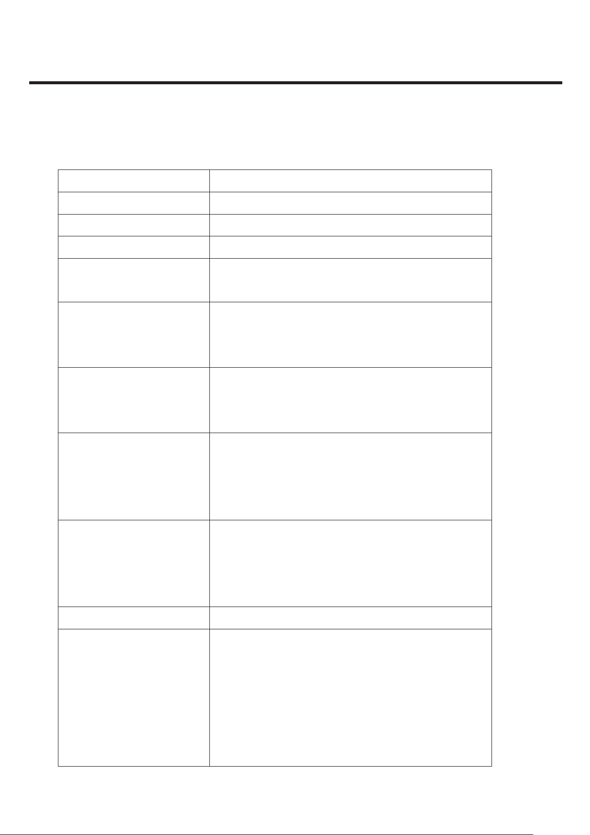
3.5 Checking WCDMA Block
3. TROUBLE SHOOTING
START
Check XO Block Refer to 3.3
Check FEMID Block Refer to 3.4
Check RF TRX Level
Re-download & Cal
LGE Internal Use Only
- 31 -
Copyright © 2014 LG Electronics. Inc. All right reserved.
Only for training and service purposes
Page 32

3.5.1 Checking XO (19.2MHz) Block
Refer to 3.3
3.5.2 Checking FEMID Block
Refer to 3.4
3.5.3 Checking RF TX Level
{WCDMA B1}
3. TROUBLE SHOOTING
LGE Internal Use Only
<Main Bot>
- 32 -
TP1
Copyright © 2014 LG Electronics. Inc. All right reserved.
Only for training and service purposes
Page 33

3. TROUBLE SHOOTING
R1108
SW101
ANT
1
G3 G4
COMMON
43
2
TP1
10K
R1107
4.7K
100pC1165
L1148
27n
RADIATION_PWR_ANT
C1164
L1140
15n
100p
5
G12G23G3
IN
OUT
4
881.5MHz
L1107 DNI
SWAP the RX Filter
G850
G900
1
FL1101
EAM62732801
EAM62732901
R1110
3.3M
G1
ANTG2
SW1100
C1160 100p
DNIL1137
L1136 DNI
VREG_L6_1V8
R1109
750KTOL=0.01
C1163
100p
WTR_PRX_LB_2_IN
L1102
1.2n
C1101
18p
L1101
100n
100pC1107
C1108 100p100pC1106
L1108 DNI
LGE Internal Use Only
TP2
TP3
<Main Top>
- 33 -
Copyright © 2014 LG Electronics. Inc. All right reserved.
Only for training and service purposes
Page 34

+VPA0
3. TROUBLE SHOOTING
CPL_IN_OUT
+VPA_BATT0
C1675 DNI
L1616 1n
DNIC1666
DNIC1607
TP2
C1613
10u
DRBFM
C1614
10n
TOL=0.01
R1600 51
Chenck ANT_Logic Refer to 3.4
Check TP1
Over 21 dBm?
EAN62687101
VEN
CPL_OUT
6
GND
7
CPL_IN
8
RFOUT
9
VCC2
10
PGND
11
SKY77761
VMODE_0
VMODE_1
RFIN
VCC1
U1600
5
4
3
2
1
DNIC1608
DNIC1610
C1609 DNI
PA0_ON_1
PA0_R_0
PA0_R_1
C1617
10u
C1618
1.5n
100pC1676
100pC1672
FL1603
4 1
DNIC1673
OUT
5 3 2
C1669 DNI
1950MHz
FL1603 => DNI
100pC1671
WTR_TX2_OUT
C1674 DNI
IN
G1G2G3
DNIC1670
TP3
Yes
RF Tx Level is OK
LGE Internal Use Only
No
Check TP2
Over 21 dBm?
No
Check TP3
Over ‐3dBm?
No
Check WTR2605
Yes
Yes
- 34 -
Check FL1600
Check PAM
Copyright © 2014 LG Electronics. Inc. All right reserved.
Only for training and service purposes
Page 35

PAM control signal
CPL_IN_OUT
PA0_ON_1 (C1608) : PAM Enable
PA0_R0 (C1609) : PAM Gain Control
PA0_R1 (C1610) : PAM Gain Control
3. TROUBLE SHOOTING
+VPA0
C1613
10u
DRBFM
C1614
10n
TP1
TP2
DNIC1666
TP3
<Main Top>
+VPA_BATT0
EAN62687101
CPL_OUT
6
GND
7
CPL_IN
8
RFOUT
9
VCC2
10
PGND
TOL=0.01
R1600 51
11
SKY77761
VEN
VMODE_0
VMODE_1
RFIN
VCC1
U1600
TP1
5
4
3
2
1
DNIC1608
DNIC1610
TP3
C1609 DNI
TP2
PA0_ON_1
PA0_R_0
PA0_R_1
C1617
10u
C1618
1.5n
100pC1676
100pC1672
DNIC1673
C1669 DNI
LGE Internal Use Only
- 35 -
Copyright © 2014 LG Electronics. Inc. All right reserved.
Only for training and service purposes
Page 36

PA LOGIC B1/B4
POWER MODE PA0_ON_1 PA0_R0 PA0_R1
SHUT DOWN L L L
STAND-BY L - -
HP MODE H L L
MP MODE H H L
LP MODE H H H
3. TROUBLE SHOOTING
LGE Internal Use Only
- 36 -
Copyright © 2014 LG Electronics. Inc. All right reserved.
Only for training and service purposes
Page 37

[WCDMA B2]
3. TROUBLE SHOOTING
TP1
<Main Bot>
R1108
SW101
ANT
1
G3 G4
COMMON
43
2
TP1
10K
R1107
4.7K
100pC1165
L1148
27n
RADIATION_PWR_ANT
C1164
L1140
15n
100p
5
G12G23G3
IN
OUT
4
881.5MHz
L1107 DNI
SWAP the RX Filter
G850
G900
1
FL1101
EAM62732801
EAM62732901
R1110
3.3M
G1
ANTG2
SW1100
C1160 100p
DNIL1137
L1136 DNI
VREG_L6_1V8
R1109
750KTOL=0.01
C1163
100p
WTR_PRX_LB_2_IN
L1102
1.2n
C1101
18p
L1101
100n
100pC1107
C1108 100p100pC1106
L1108 DNI
LGE Internal Use Only
- 37 -
Copyright © 2014 LG Electronics. Inc. All right reserved.
Only for training and service purposes
Page 38

TX_MODULE_TRX_2
WTR_PRX_LB_1_IN
3. TROUBLE SHOOTING
TP2
L1618
1n
L1607 DNI
L1617 DNI
FL1601 EAM62890101
ANT
GND1 GND6
GND2 GND5
GND3 GND4
RX
TX
16
3
92
84
75
LNA_PRX_MB2_IN
L1619 2.7n
C1645 1.2p
C1646 1p
TX_MODULE_TRX_4
+VPA0
C1635
10u
EAM62711101FL1602
6
ANT
GND12GND6
GND24GND5
GND35GND4
RX
TX
DNIL1608
27pC1650
6.8nL1620
CPL_IN_OUT
1nC1632
10nC1633
C1634
C1636 10n
C1637 1n
15
14
GND6
CPLIN
RFOUTHB
U1602
SKY77742-21
EAN62885901
GND3
CPLOUT
GND2
9
16
738
1
VBATT
GND1
6
RFIN
VENHB
VENLB
VMODERFOUTLB
17
PGND
13
GND5
12
VCC
11
GND4
10 5
10u
2
4
DNIC1648
DNIC1647
1
3
9
8
7
+VPA_BATT0
C1649 DNI
C1652 100p
PA0_ON_0
PA0_ON_2
PA0_R_0
C1641 100p
L1627 15n
C1653 DNI
Shunt cap must be<=33pF
guarantee LNA gain setting time
TP3
C1642 100p
DNI
C1643
WTR_TX3_OUT
L1626 4.7n
1pC1654
DNIL1610
B2, B5, B8
LGE Internal Use Only
WTR_PDET_IN
- 38 -
Copyright © 2014 LG Electronics. Inc. All right reserved.
Only for training and service purposes
Page 39

TP2
3. TROUBLE SHOOTING
TP3
<Main Top>
LGE Internal Use Only
- 39 -
Copyright © 2014 LG Electronics. Inc. All right reserved.
Only for training and service purposes
Page 40

Check Ant Logic Refer to 3.4
3. TROUBLE SHOOTING
Check TP1
Over 21 dBm?
No
Check TP2
Over 21 dBm?
No
Check TP3
Over ‐3dBm?
No
Check WTR2605
Yes
RF Tx Level is OK
Yes
Check FL1601
Yes
Check PAM
LGE Internal Use Only
- 40 -
Copyright © 2014 LG Electronics. Inc. All right reserved.
Only for training and service purposes
Page 41

PAM control signal
PA0_ON_0 (C1647) : PAM Enable & Band Select
PA0_ON_2 (C1648) : PAM Enable & Band Select
PA0_R_0 (C1648) : Gain Control
3. TROUBLE SHOOTING
TP1
TP3
TP2
<Main Top>
LGE Internal Use Only
- 41 -
Copyright © 2014 LG Electronics. Inc. All right reserved.
Only for training and service purposes
Page 42

+VPA0
C1635
10u
3. TROUBLE SHOOTING
CPL_IN_OUT
1nC1632
10nC1633
C1634
C1636 10n
C1637 1n
10u
+VPA_BATT0
15
14
GND6
CPLIN
RFOUTHB
U1602
SKY77742-21
EAN62885901
GND3
CPLOUT
GND2
9
1
16
VBATT
VENHB
VENLB
VMODERFOUTLB
GND1
6
738
WTR_PDET_IN
RFIN
17
PGND
13
GND5
12
VCC
11
GND4
10 5
TP1
2
4
DNIC1648
DNIC1647
TP2
PA0_ON_0
PA0_ON_2
PA0_R_0
TP3
C1649 DNI
C1641 100p
C1642 100p
DNI
C1643
WTR_TX3_OUT
B2, B5, B8
PA LOGIC B2/B5
POWER MODE PA_ON_0 PA_ON_2 PA0_R0
SHUT DOWN L L L
STAND-BY L L -
B1/B2 HPM H L L
B1/B2 LPM H L H
B5/B8 HPM L H L
B5/B8 LPM L H H
LGE Internal Use Only
- 42 -
Copyright © 2014 LG Electronics. Inc. All right reserved.
Only for training and service purposes
Page 43

[WCDMA B8]
3. TROUBLE SHOOTING
TP1
<Main Bot>
R1108
SW101
ANT
1
G3 G4
COMMON
43
2
TP1
10K
R1107
4.7K
100pC1165
L1148
27n
RADIATION_PWR_ANT
C1164
L1140
15n
100p
5
G12G23G3
IN
OUT
4
881.5MHz
L1107 DNI
SWAP the RX Filter
G850
G900
1
FL1101
EAM62732801
EAM62732901
R1110
3.3M
G1
ANTG2
SW1100
C1160 100p
DNIL1137
L1136 DNI
VREG_L6_1V8
R1109
750KTOL=0.01
C1163
100p
WTR_PRX_LB_2_IN
L1102
1.2n
C1101
18p
L1101
100n
100pC1107
C1108 100p100pC1106
L1108 DNI
LGE Internal Use Only
- 43 -
Copyright © 2014 LG Electronics. Inc. All right reserved.
Only for training and service purposes
Page 44

3. TROUBLE SHOOTING
TX_MODULE_TRX_2
L1618
1n
L1607 DNI
L1617 DNI
FL1601 EAM62890101
ANT
GND1 GND6
GND2 GND5
GND3 GND4
RX
TX
16
3
92
84
75
LNA_PRX_MB2_IN
L1619 2.7n
C1645 1.2p
C1646 1p
TP2
EAM62711101FL1602
6
ANT
GND12GND6
GND24GND5
GND35GND4
RX
TX
DNIL1608
27pC1650
6.8nL1620
TX_MODULE_TRX_4 WTR_PRX_LB_1_IN
C1652 100p
1
3
9
8
7
L1627 15n
L1626 4.7n
1pC1654
C1653 DNI
Shunt cap must be<=33pF
guarantee LNA gain setting time
DNIL1610
+VPA0
C1635
10u
C1636 10n
LGE Internal Use Only
CPL_IN_OUT
1nC1632
10nC1633
C1634
10u
C1637 1n
17
PGND
1
15
16
14
GND6
CPLIN
VBATT
+VPA_BATT0
TP3
RFOUTHB
13
GND5
12
VCC
11
GND4
10 5
U1602
SKY77742-21
EAN62885901
GND3
CPLOUT
GND2
9
GND1
738
6
RFIN
VENHB
VENLB
VMODERFOUTLB
2
4
DNIC1648
DNIC1647
PA0_ON_0
PA0_ON_2
PA0_R_0
C1649 DNI
C1641 100p
C1642 100p
DNI
C1643
WTR_TX3_OUT
B2, B5, B8
WTR_PDET_IN
- 44 -
Copyright © 2014 LG Electronics. Inc. All right reserved.
Only for training and service purposes
Page 45

TP2
TP3
3. TROUBLE SHOOTING
<Main Top>
LGE Internal Use Only
- 45 -
Copyright © 2014 LG Electronics. Inc. All right reserved.
Only for training and service purposes
Page 46

Check Ant Logic Refer to 3.4
3. TROUBLE SHOOTING
Check TP1
Over 21 dBm?
No
Check TP2
Over 21 dBm?
No
Check TP3
Over ‐3dBm?
No
Check WTR2605
Yes
RF Tx Level is OK
Yes
Check FL1602
Yes
Check PAM
LGE Internal Use Only
- 46 -
Copyright © 2014 LG Electronics. Inc. All right reserved.
Only for training and service purposes
Page 47

PAM control signal
PA0_ON_0 (C1647) : PAM Enable & Band Select
PA0_ON_2 (C1648) : Gain Control
PA0_R_0 (C1648) : Gain Control
3. TROUBLE SHOOTING
TP1
TP3
TP2
<Main Top>
LGE Internal Use Only
- 47 -
Copyright © 2014 LG Electronics. Inc. All right reserved.
Only for training and service purposes
Page 48

+VPA0
C1635
10u
3. TROUBLE SHOOTING
CPL_IN_OUT
1nC1632
10nC1633
C1634
C1636 10n
C1637 1n
10u
+VPA_BATT0
15
14
CPLIN
RFOUTHB
U1602
EAN62885901
GND3
CPLOUT
9
16
GND6
GND2
738
1
VBATT
GND1
6
RFIN
VENHB
VENLB
VMODERFOUTLB
WTR_PDET_IN
17
PGND
13
GND5
12
VCC
11
10 5
GND4
SKY77742-21
TP1
2
4
DNIC1648
DNIC1647
TP2
PA0_ON_0
PA0_ON_2
PA0_R_0
TP3
C1649 DNI
C1641 100p
C1642 100p
DNI
C1643
WTR_TX3_OUT
B2, B5, B8
PA LOGIC B2/B5
POWER MODE PA_ON_0 PA_ON_2 PA0_R0
SHUT DOWN L L L
STAND-BY L L -
B1/B2 HPM H L L
B1/B2 LPM H L H
B5/B8 HPM L H L
B5/B8 LPM L H H
LGE Internal Use Only
- 48 -
Copyright © 2014 LG Electronics. Inc. All right reserved.
Only for training and service purposes
Page 49

3.5.4 Checking RF Rx Level
[WCDMA B1]
3. TROUBLE SHOOTING
Test Point (WCDMA B1 RF Rx Level)
TP1
R1108
SW101
ANT
1
G3 G4
COMMON
43
2
TP1
10K
R1107
4.7K
100pC1165
L1148
27n
RADIATION_PWR_ANT
C1164
L1140
15n
100p
5
G12G23G3
IN
OUT
4
881.5MHz
L1107 DNI
SWAP the RX Filter
G850
G900
1
FL1101
EAM62732801
EAM62732901
R1110
3.3M
G1
ANTG2
SW1100
C1160 100p
DNIL1137
L1136 DNI
VREG_L6_1V8
R1109
750KTOL=0.01
C1163
100p
WTR_PRX_LB_2_IN
L1102
1.2n
C1101
18p
L1101
100n
100pC1107
C1108 100p100pC1106
L1108 DNI
LGE Internal Use Only
- 49 -
Copyright © 2014 LG Electronics. Inc. All right reserved.
Only for training and service purposes
Page 50

TP2
3. TROUBLE SHOOTING
<Main Top>
TX_MODULE_TRX_1 LNA_PRX_MB1_IN
DNIL1600
2.2nL1621
L1615 2.7n
6
ANT
GND12GND6
GND24GND5
GND35GND4
EAM62711201FL1600
1
RX
3
TX
9
8
7
TP2
B1, B4
L1616 1n
C1675 DNI
DNIC1607
+VPA0
C1613
10u
LGE Internal Use Only
- 50 -
Copyright © 2014 LG Electronics. Inc. All right reserved.
Only for training and service purposes
Page 51

START
3. TROUBLE SHOOTING
No
Check TP1 Signal exist ?
Check TP2 Signal exist ?
Check WTR2605
Check RF Switch (M/S)
Yes
No
Check FL1600
Yes
LGE Internal Use Only
- 51 -
Copyright © 2014 LG Electronics. Inc. All right reserved.
Only for training and service purposes
Page 52

[WCDMA B2]
3. TROUBLE SHOOTING
Test Point (WCDMA B2 RF Rx Level)
TP1
R1108
SW101
ANT
1
G3 G4
COMMON
43
2
TP1
10K
R1107
4.7K
100pC1165
L1148
27n
RADIATION_PWR_ANT
C1164
L1140
15n
100p
5
G12G23G3
IN
OUT
4
881.5MHz
L1107 DNI
SWAP the RX Filter
G850
G900
1
FL1101
EAM62732801
EAM62732901
R1110
3.3M
G1
ANTG2
SW1100
C1160 100p
DNIL1137
L1136 DNI
VREG_L6_1V8
R1109
750KTOL=0.01
C1163
100p
WTR_PRX_LB_2_IN
L1102
1.2n
C1101
18p
L1101
100n
100pC1107
C1108 100p100pC1106
L1108 DNI
LGE Internal Use Only
- 52 -
Copyright © 2014 LG Electronics. Inc. All right reserved.
Only for training and service purposes
Page 53

TP2
WTR_PRX_LB_1_IN
3. TROUBLE SHOOTING
TX_MODULE_TRX_2
TX_MODULE_TRX_4
<Main Top>
TP2
L1618
1n
L1607 DNI
DNIL1608
L1617 DNI
27pC1650
6.8nL1620
FL1601 EAM62890101
ANT
GND1 GND6
GND2 GND5
GND3 GND4
EAM62711101FL1602
6
ANT
GND12GND6
GND24GND5
GND35GND4
16
RX
3
TX
92
84
75
C1652 100p
1
RX
3
TX
9
8
7
LNA_PRX_MB2_IN
L1619 2.7n
C1645 1.2p
L1627 15n
L1626 4.7n
C1653 DNI
Shunt cap must be<=33pF
guarantee LNA gain setting time
1pC1654
C1646 1p
DNIL1610
LGE Internal Use Only
- 53 -
Copyright © 2014 LG Electronics. Inc. All right reserved.
Only for training and service purposes
Page 54

START
3. TROUBLE SHOOTING
No
Check TP1 Signal exist ?
Check TP2 Signal exist ?
Check WTR2605
Check RF Switch (M/S)
Yes
No
Check FL1601
Yes
LGE Internal Use Only
- 54 -
Copyright © 2014 LG Electronics. Inc. All right reserved.
Only for training and service purposes
Page 55

[WCDMA B8]
3. TROUBLE SHOOTING
Test Point (WCDMA B8 RF Rx Level)
TP1
R1108
SW101
ANT
1
G3 G4
COMMON
43
2
TP1
10K
R1107
4.7K
100pC1165
L1148
27n
RADIATION_PWR_ANT
C1164
L1140
15n
100p
5
G12G23G3
IN
OUT
4
881.5MHz
L1107 DNI
SWAP the RX Filter
G850
G900
1
FL1101
EAM62732801
EAM62732901
R1110
3.3M
G1
ANTG2
SW1100
C1160 100p
DNIL1137
L1136 DNI
VREG_L6_1V8
R1109
750KTOL=0.01
C1163
100p
WTR_PRX_LB_2_IN
L1102
1.2n
C1101
18p
L1101
100n
100pC1107
C1108 100p100pC1106
L1108 DNI
LGE Internal Use Only
- 55 -
Copyright © 2014 LG Electronics. Inc. All right reserved.
Only for training and service purposes
Page 56

TP2
3. TROUBLE SHOOTING
<Main Top>
TX_MODULE_TRX_2
TX_MODULE_TRX_4 WTR_PRX_LB_1_IN
L1618
1n
L1607 DNI
DNIL1608
L1617 DNI
27pC1650
6.8nL1620
FL1601 EAM62890101
ANT
GND1 GND6
GND2 GND5
GND3 GND4
EAM62711101FL1602
6
ANT
GND12GND6
GND24GND5
GND35GND4
16
RX
3
TX
92
84
75
C1652 100p
1
RX
3
TX
9
8
7
TP2
LNA_PRX_MB2_IN
L1627 15n
C1653 DNI
L1619 2.7n
C1645 1.2p
L1626 4.7n
1pC1654
C1646 1p
DNIL1610
LGE Internal Use Only
- 56 -
Shunt cap must be<=33pF
guarantee LNA gain setting time
Copyright © 2014 LG Electronics. Inc. All right reserved.
Only for training and service purposes
Page 57

START
3. TROUBLE SHOOTING
No
Check TP1 Signal exist ?
Check TP2 Signal exist ?
Check WTR2605
Check RF Switch (M/S)
Yes
No
Check FL1602
Yes
LGE Internal Use Only
- 57 -
Copyright © 2014 LG Electronics. Inc. All right reserved.
Only for training and service purposes
Page 58

3.6 Checking GSM Block
3. TROUBLE SHOOTING
START
Check XO Block Refer to 3.3
Check FEMID Block Refer to 3.4
Check RF TRX Level
Re-download & Cal
LGE Internal Use Only
- 58 -
Copyright © 2014 LG Electronics. Inc. All right reserved.
Only for training and service purposes
Page 59

3.6.1 Checking TCXO Block
Refer to 3.3
3.6.2 Checking Tx module Block
Refer to 3.4
3.6.3 Checking RF TX level
3. TROUBLE SHOOTING
G1
ANTG2
SW1100
WTR_TX1_OUT
TP2
C1160 100p
L1136 DNI
VREG_L6_1V8
+VPA_BATT0
TX_MODULE_TRX_1
TX_MODULE_TRX_2
TX_MODULE_TRX_4
C1145 3.9p
8.2nL1129
8.2nL1128
DNIL1137
SW101
ANT
1
G3 G4
COMMON
43
2
TP1
10K
R1108
R1109
750KTOL=0.01
C1163
100p
R1110
3.3M
WTR_PRX_LB_2_IN
GND15
22
GND16
23
TRX1
24
GND17
25
TRX2
26
GND18
27
TRX3
28
GND19
29
TRX4
30
GND20
31
VBATT
32
NC1
C1110
4.7u
for W7 CI (06/07)
DNIC1121
DNIC1120
33
22pC1109
SPDT_SEL
ANT0_SW_SEL_0
ANT0_SW_SEL_1 ANT0_SW_SEL_2
C1119 DNI
C1164
100p
L1140
15n
18
202119
RX1
RX2
GND14
SPDT_IN
SPDT_OUT
EAT62073401
SKY77573-31
U1100
RF_IN
SPDT
SW1
NC2
SW0
34
GND13
HB_EN
L1107 DNI
15
141617
13
ANT
GND11
GND12
GND10
GND9
GND8
GND7
GND6
GND5
GND4
VCC2
VCC1
GND3
GND2
GND1
PGND
LB_EN
MODE0
MODE1
434241403937383536
DNIC1115
C1116 DNI
100pC1165
R1107
4.7K
RADIATION_PWR_ANT
5
G12G23G3
OUT
4
FL1101
881.5MHz
SWAP the RX Filter
G850
G900
12
11
10
9
8
7
6
5
4
3
2
1
C1117 DNI
RX_G1800
RX_G1900
DNIC1118
L1138 2n
100p
C1112
C1113 10u
L1148
27n
IN
1
EAM62732801
EAM62732901
2nL1139
DNIL1105
L1106 DNI
C1114 0.1u
PA0_R_1
PA0_R_0
ANT0_SW_SEL_3
L1102
1.2n
100pC1107
+VPA_BATT0
C1101
18p
L1101
100n
C1108 100p100pC1106
L1108 DNI
LGE Internal Use Only
Schematic of GSM(850/900)/DCS/PCS Tx Block
- 59 -
Copyright © 2014 LG Electronics. Inc. All right reserved.
Only for training and service purposes
Page 60

3. TROUBLE SHOOTING
TP2
TP1
<Main Bot>
LGE Internal Use Only
<Main Top>
- 60 -
Copyright © 2014 LG Electronics. Inc. All right reserved.
Only for training and service purposes
Page 61

Start
Check XO Block Refer to 3.3
3. TROUBLE SHOOTING
Check TP1
If GSM over 31 dBm ?
If DCS/PCS over 28 dBm ?
No
Check TP2, 3
If GSM(TP2) under 6 dBm ?
If DCS/PCS(TP2) under 6 dBm ?
No
Check WTR2605
Yes
Yes
GSM Tx is OK
Check the other part
Check Tx Module
LGE Internal Use Only
- 61 -
Copyright © 2014 LG Electronics. Inc. All right reserved.
Only for training and service purposes
Page 62

3.6.4 Checking RF Rx Block
3. TROUBLE SHOOTING
TP1
<Main Bot>
R1108
SW101
ANT
1
G3 G4
10K
COMMON
43
2
TP1
R1107
4.7K
100pC1165
L1148
27n
RADIATION_PWR_ANT
C1164
L1140
15n
100p
L1107 DNI
TP2
5
G12G23G3
IN
OUT
4
881.5MHz
1
FL1101
SWAP the RX Filter
G850
G900
EAM62732801
EAM62732901
R1110
3.3M
G1
ANTG2
SW1100
C1160 100p
DNIL1137
L1136 DNI
VREG_L6_1V8
R1109
750KTOL=0.01
C1163
100p
WTR_PRX_LB_2_IN
L1102
1.2n
C1101
18p
L1101
100n
100pC1107
C1108 100p100pC1106
L1108 DNI
LGE Internal Use Only
- 62 -
Copyright © 2014 LG Electronics. Inc. All right reserved.
Only for training and service purposes
Page 63

TP3
3. TROUBLE SHOOTING
TP2
RX_G1800
RX_G1900
L1138 2n
TP4
<Main Top>
FL1100
GSM1800_OUT
6
GND5
7
GND6
2nL1139
DNIL1105
L1106 DNI
8
GSM1900_OUT
9
510
GND7 GND4
GND3
GND2
GND1
GSM1800/1900_IN
4
3
2
1
TP3
C1150 100pC1149 100p
DNI
C1152
G1800, G1900
WTR_PRX_MB_3_IN
LGE Internal Use Only
- 63 -
Copyright © 2014 LG Electronics. Inc. All right reserved.
Only for training and service purposes
Page 64

3. TROUBLE SHOOTING
EAM62711101FL1602
6
ANT
GND12GND6
GND24GND5
GND35GND4
RX
TX
DNIL1608
27pC1650
6.8nL1620
TX_MODULE_TRX_4 WTR_PRX_LB_1_IN
C1652 100p
1
3
9
8
7
TP4
L1627 15n
L1626 4.7n
1pC1654
C1653 DNI
Shunt cap must be<=33pF
guarantee LNA gain setting time
DNIL1610
Schematic of GSM(850/900)/DCS/PCS Rx Block
Set the Phone Rx is ON
Check TP1 Signal exist ?
Yes
Check TP2,3,4 Signal exist ?
Yes
Check WTR2605
No
Check RF Switch (M/S)
No
Check Tx Module
LGE Internal Use Only
- 64 -
Copyright © 2014 LG Electronics. Inc. All right reserved.
Only for training and service purposes
Page 65

3.7 GPS Trouble Shooting
20
21
40
13
24
D9500
C2387
D7301
C7303
R9600
R3301
R3302
L6811
LD9830
R3308
R7203
FB6611
R6613
ZD6613
U4134
VA9506
R9603
L6810
J6610
C8950
D9503
R6612
R7304
ZD6610
R6617
D7302
R9604
R2319
C4185
C6622
D6811
C7302
R7301
ZD6611
FB6612
R7201
R7300
C2386
FB6100
C9503
VA9504
CN7200
R9602
C9504
R2104
R8950
VA9503
C4184
R2102
CN7300
R3304
ZD6612
D9504
C6611
C7300
C7305
C6812
VA9505
C6623
FB6610
C9505
VA7303
C2368
C6810
R9504
D9501
D9505
C7301
C7304
3.7.1 GPS IC Component
C7400
R2207
L1125
L1146
L1126
BAT4130
R2202
R2201
TP8101
TP8100
U8100
C8101
GPS LNA
U1
L1127
C1161
L1147
C7403
R7401
ZD8401
ZD8400
C4123
C4156
C4189
C4194
C4159
R1105
CN1102
CN7400
ANTENNA CONTACT
L1124
C1144
L1120
CN1103
L1121
C7103
C7102
13
24
C7104
C7105
R5200
L1144
VA7101
VA7100
12
CN7100
C5201
L1131
C7100
C7101
VA7103
VA7102
C4197
FL7102
R7101
R5205
C1159
L1132
FL7103
C5217
C5207
1120
10
FL1105
Saw Filter
FL7101
3. TROUBLE SHOOTING
C8400
C8401
R8401
VA7404
VA7403
R2208
C7401
C7402
C8100
FL7400
C1142
C1141
FB1140
L1118
C1143
L1135
ZD9830
L1130
R7305
R7306
C4165
C4131
R4105
R4142
C4132
C4198
C4124
C4145
C4166
C6811
D6810
R8400
C4147
C4181
C4180
U4132
C4179
C4178
U4131
C4182
C4183
U4133
R7303
R9601
U1500
WTR2605
<Min Bot> <Min Top>
Reference Description
CN1103 ANTENNA CONTACT
FL1105 Saw Filter
U1 GPS LNA
U1500 WTR2605
LGE Internal Use Only
- 65 -
Copyright © 2014 LG Electronics. Inc. All right reserved.
Only for training and service purposes
Page 66

3. TROUBLE SHOOTING
CN5101
C5224
C1113
CN5100
R5125
C5123
SW101
C1112
C1116
C1114
R3301
L6811
R3304
C6810
D6811
C6812
R3302
R3308
L6810
C8400
C8401
R8401
C6811
R2208
C4165
C4193
R4110
C9108
ZD9100
C7402
FL7400
C1141
L1118
L1135
ZD9830
R7305
R7306
C4131
R4105
R4142
R4104
R4114
C4105
C9506
D6810
C7401
R8400
C4147
C4181
C4180
U4132
C4179
C4178
U4131
C4182
C4183
C4184
U4133
U4134
C4185
R7304
R7303
C1142
FB1140
LD9830
C1143
D9504
D9505
D9503
R9601
J9600
R9600
D9500
R9602
R9603
D9501
R9604
D9502
C2377
C2374
C2379
C4136
C2375
C2367
R4133
R4107
C4140
R4108
R4210
C4195
VA9100
R1401
R9109
R9111
C7305
C7304
C2382
C2381
C2380
C2389
C2388
C2394
C2309
C4196
R4209
R1400
C7302
C7303
R7300
24
CN7300
C2373
FL7300
C2378
C2376
C2392
C2391
C2308
C2302
C2305
C4138
C2300
C2304
C2301
R4132
C2306
C4141
VA7303
R2104
R2102
D7302
D7301
R7301
C7300
C7301
13
C2387
C2386
C2368
R2319
C2390
12
L2300
FL7302
FL7301
C2307
C2366
C2303
C2344
C2358
C2369
C2343
C2341
C2365
C2345
C2355
C2372
C2354
C2371
C2352
C2346
C2340
C2353
C2342
C2370
C2356
C2337
C2338
C2339
C4132
C4198
C9600
C4103
VA9513
R9606
R9605
VA7404
VA7403
C7400
R2207
R1105
CN1102
CN7400
L1124
C1144
L1120
CN1103
13
24
C7104
C7105
R9502
R9503
TP5200
TP5201
C5231
R5230
C5230
C5205
C5206
L1121
C7103
C7102
CN7100
R5200
C5200
C5222
C5220
C5215
C5218
L5200
C5204
C5202
ANT5202
VA7101
L1144
VA7100
12
C5201
U5200
7
C5211
L1131
C7100
C7101
VA7103
VA7102
C4197
R7101
R5205
L5201
C5214
C5210
C1159
L1132
FL7103
FL7102
C5217
C5207
R4112
F
E
D
C
B
A
1
C5216
C5209
C5232
D9100
1120
10
FL1105
FL7101
C4104
Q5200
C5219
C5223
R5206
C9106
C9105
R5204
L1125
L1146
L1126
BAT4130
TP5204
TP5203
C4122
R9104
U8100
C8101
U1
L1127
C1161
C7403
R7401
R2202
ZD8400
R2201
C4156
C4189
C4159
C4157
TP5202
TP4100
C9100
FL9100
TP8101
TP8100
C8100
L1130
L1147
C4124
ZD8401
C4145
C4123
C4194
C4166
C4148
C4192
C4162
C4153
C2100
C4187
C4188
R9107
C9107
R9108
R9106
R6617
FB6100
R8950
C8950
R7203
R7201
C6611
R6613
20
R6612
R9504
FB6610
ZD6610
40
ZD6613
FB6612
CN7200
C6623
ZD6612
C6622
FB6611
21
ZD6611
VA9505
C9504
C9503
VA9506
VA9504
J9500
J6610
C9505
R9501
VA9503
C5122
D5100
C5120
C5100
C1121
C1120
C1115
C1118
C1117
C1119
C1101
L1101
L1102
L1148
C1165
R1107
ANT2500
CN9100
<Min Bot>
GPS Signal
LGE Internal Use Only
- 66 -
Copyright © 2014 LG Electronics. Inc. All right reserved.
Only for training and service purposes
Page 67

3.7.2 Checking GPS
START
3. TROUBLE SHOOTING
ANT 1103 : Ant. Contact
U1 : GPS LNA
FL1105 : SAW Filter
U1500 : WTR2605
U4100 : PM8226
X4100 : Crystal
No
Check ANT1103
Check TP1
R11002 is 1.8v
L11014 is 2.7v
Check TP2
Signal exist?
Check WTR2605
Remove the foreign substance inANT1103
Yes
No
Check U4100
Yes
No
Check X4100
Yes
LGE Internal Use Only
- 67 -
Copyright © 2014 LG Electronics. Inc. All right reserved.
Only for training and service purposes
Page 68

3.7.3 Photo/Circuit
3. TROUBLE SHOOTING
TP1
GNSS_ELNA_EN
L1146 8.2n
L1126
DNI
<Main Bot>
L1135
22n
100pC1143
TP1
2
RFIN
DNI
L1125
L1118
22n
7
1
VCTRL
U1
SFMG2BAD001
GND3
GND1
GND2
3
6
4
8
C1141 100p
VDD
RFOUT
GND4
Schematic of GPS LNA Block
FB1140
5
?
VREG_L14_2V75
6.3V
C1142 0.1u
L1147 2.2n
DNIL1130
L1127 10n
C1161 100p
WTR_GNSS_RF_IN_1
LGE Internal Use Only
- 68 -
Copyright © 2014 LG Electronics. Inc. All right reserved.
Only for training and service purposes
Page 69

TP2
3. TROUBLE SHOOTING
U4100
X4100
WTR0_XO_IN
C1508
100p
<Main Top>
TP2
option)
R1504
51 TOL=0.01
WTR_XO_IN
C1513 DNI
LGE Internal Use Only
- 69 -
Copyright © 2014 LG Electronics. Inc. All right reserved.
Only for training and service purposes
Page 70

3.8 WIFI/BT Trouble Shooting
3.8.1 WIFI/BT IC Component
CN5100
Connected to antenna
FL5100
Saw
Filter
3. TROUBLE SHOOTING
U5100
WCN3620
<Min Bot> <Min Top>
Reference Description
CN5100
FL5100 Saw Filter
U5100 WCN3620
Connected to antenna
C-Clip
LGE Internal Use Only
- 70 -
Copyright © 2014 LG Electronics. Inc. All right reserved.
Only for training and service purposes
Page 71

3.8.2 WIFI/BT Signal Path Tx/Rx
To opposite side
3. TROUBLE SHOOTING
<Min Bot> <Min Top>
WIFI,BTSignal
LGE Internal Use Only
- 71 -
Copyright © 2014 LG Electronics. Inc. All right reserved.
Only for training and service purposes
Page 72

3.8.3 WIFI/BT Signal Path Tx
3. TROUBLE SHOOTING
START
Check ANT5100
Check TP1,2,3,4
TP1 C5100 is 1.8v
TP2 C5101 is 1.8v
TP3 C5224 is 1.3v
TP4 R5105 is 3.3v
Check U5100
ANT5100 : Ant. Contact
U5100 : WCN3620
U4100 : PM8226
No
Remove the foreign substance
inANT1103
Yes
No
Check U4100
Yes
Test point Net name Description
TP1 VREG_L6_1V8 Power for WCN Digital I/O circuits
TP2 VREG_L10_1V8 Power for XO circuitinput voltage.
TP3 VREG_L24_1V3
TP4 VREG_L16_3V3 Power for WLAN 2.4GHz PA circuits
LGE Internal Use Only
- 72 -
Power for WCN analog, digital,and RF core circuits.
Power for WLAN driver amplier circuits
Copyright © 2014 LG Electronics. Inc. All right reserved.
Only for training and service purposes
Page 73

3. TROUBLE SHOOTING
CN5100
TP1
TP3
TP2
<Main Bot>
TP4
U5100
LGE Internal Use Only
<Main Top>
- 73 -
Copyright © 2014 LG Electronics. Inc. All right reserved.
Only for training and service purposes
Page 74

VREG_L6_1V8
VREG_L10_1V8
3. TROUBLE SHOOTING
VREG_L24_1V3
TP3
C5224
DNI
TP1
TP2
6.3V
6.3V
C5100
C5101
470n
470n
C5102
4.7u
6.3V C5105
22n
10V
10nC5107
10V
10V
10n
C5109
10V
10n
C5111
FB5100
240
C5114
100p
10nC5108
C5112
10u
C5113
100p
C5115
10u
R5104
22
VDD_IO_1P8
24
VDD_XO_1P8
29
VDD_DIG_1P2
56
VDD_FM_RXFE_1P3
57
VDD_FM_RXBB_1P3
52
VDD_FM_PLL_1P3
51
VDD_FM_VCO_1P3
3
VDD_BT_RF_1P3
13
VDD_BT_BB_1P3
16
VDD_BT_PLL_1P3
7
VDD_BT_VCO_1P3
23
VDD_BT_FM_DIG_1P3
60
VDD_WL_BB_1P3
37
VDD_WL_2GPA_1P3
43
VDD_WL_UPC_1P3
9
VDD_WL_2GLNA_1P3
58
VDD_WL_PLL_1P3
36
VDD_WL_LO_1P3
11
VDD_WL_2GPA_3P3
4
VDD_BT_DA_3P3
C5116
100p
0
TP4
Schematic of WCN3620
VREG_L16_3V3
0R5105
LGE Internal Use Only
- 74 -
Copyright © 2014 LG Electronics. Inc. All right reserved.
Only for training and service purposes
Page 75

3.9 Audio Trouble
3.9.1 Speaker troubleshooting
Speaker path as below :
MSM8226 -> WCD9302 SPKR_DRVP / SPRK_DRVN -> Speaker
START
3. TROUBLE SHOOTING
Yes
After power on, Headphone icon
display on Upper right LCD ?
No
Change Rear Cover Ass’y
Speaker Sound can hear?
No
Change Lower FPCB.
Speaker works well?
No
Check Main Board
TP1(BUCK_VSW)
TP2(VDD_SPKDRV)
No
Yes
Yes
Yes
Refer to 3.9.5 Ear-MIC troubleshooting
Rework lower FPCB
TP1(L100), TP2(L101)
Abnormal FPCB inspection
TP1 to TP2/TP2 to TP4
Short test. Is it OK?
Yes
Headphone path works well?
No
No
Yes
Fail on TP1 -> replace U6100
Fail on TP2 -> replace R6107
LGE Internal Use Only
End
- 75 -
Replace component
U2100 or main board
Copyright © 2014 LG Electronics. Inc. All right reserved.
Replace component
U6100
Only for training and service purposes
Page 76

SPEAKER
TP1(L100)
3. TROUBLE SHOOTING
SPK_P
SPK_N
Rev 1.0
C103
4.7n
C104
4.7n
L100
L101
Rev.C
size change (1005-->1608)
TP3(L101)
TP1(L100)
82n
82n
CN102
TP2
2
TP1
1
2
EAB62653001
BRS-181030P08-P
BUJEON
(06/03)
TP2
LGE Internal Use Only
TP3(L101)
- 76 -
Copyright © 2014 LG Electronics. Inc. All right reserved.
TP1
Only for training and service purposes
Page 77

U6100
1105
WCD9302
HPH_L
HPH_REF
HPH_R
LINE_OUT1
LINE_OUT2
VDD_BUCK
BUCK_VSW
BUCK_VOUT1
BUCK_VOUT2
GND_BUCK
-NCP_VNEG
NCP_C1P
-NCP_C1M
SPKR_DRVP
SPKR_DRVM
VDD_SPKDRV
GND_SPKDRV_1
GND_SPKDRV_2
GND4
3. TROUBLE SHOOTING
16
17
21
36
32
3
13
6
12
7
11
2
1
49
50
45
55
40
18
0620
FB6100
1000
1uC6108
10V
C6109 4.7u
0.2
1uC6107
TP1(FB6100)
LINE_OUT2
Note.1(06/06)
(06/27) 10V->6.3V
C6104 2.2u
C6105 4.7u
Note.2(06/06)
Dedicate a ground island for the buck/NCP ground connections.
SPK_P
SPK_N
TP2(R6107)
100pC6122
C6121 100p
HPH_REF
LINE_OUT_IRRC
LINE_OUT1
VREG_S4_2P1
R6107 0
R6108 DNI
1n
1n
C6623
C6622
+VPWR_BOOST_BYPASS
HPH_L
HPH_R
+VPWR
TP1(FB6100)
RevC)131111-FM
TP2(R6107)
LGE Internal Use Only
<Min Bot> <Min Top>
- 77 -
Copyright © 2014 LG Electronics. Inc. All right reserved.
Only for training and service purposes
Page 78

3.9.2 Receiver troubleshooting
Receiver path as below :
MSM8226 -> WCD9302 EAROP/ EAROM -> Receiver
START
3. TROUBLE SHOOTING
Run Voice Recording application.
Main Mic. Works well?
No
Refer to 3.8.3 Main MIC troubleshooting
Yes
After Change Receiver
Works well?
TP1 to TP2/TP3 to TP4
Short test. Is it OK?
Rework component
TP1(L6810), TP3(L6811)
Works well?
Yes
No
Yes
No
Yes
No
LGE Internal Use Only
- 78 -
Replace component U6100
End
Copyright © 2014 LG Electronics. Inc. All right reserved.
Only for training and service purposes
Page 79

RCV_P
RCV_N
TP1(L6810)
33p
C6810
L6810
82n
L6811
82n
TP3(L6811)
D6810
D6811
33pC6811
33pC6812
3. TROUBLE SHOOTING
CN6810
TP2
TP4
1
2
EAB62888201
EM-TECH
TP3(L6811)
TP1(L6810)
TP2
TP4
<Main Bot>
LGE Internal Use Only
- 79 -
Copyright © 2014 LG Electronics. Inc. All right reserved.
Only for training and service purposes
Page 80

3.9.3 Main MIC troubleshooting
Main Mic. path as below :
MSM8226 -> WCD9302 MIC1_INP/ MIC1_INM -> Mic
START
3. TROUBLE SHOOTING
Headphone icon display on Upper
right LCD ?
No
After Change Lower FPCB
Works well?
No
Check Mic Power in Main Board
TP1(MIC_BIAS_1)
No
Yes
Refer to 3.9.5 Ear-MIC troubleshooting
Yes Yes
Yes
Check Mic signal in Lower FPCB
TP2(MIC_IN1_P)
No
Replace component
MIC100on Lower FPCB
LGE Internal Use Only
Replace component U6100 Change Main Board
End
- 80 -
Copyright © 2014 LG Electronics. Inc. All right reserved.
Only for training and service purposes
Page 81

MIC_BIAS_1
Main_MIC
MIC_IN1_N
MIC_IN1_P
TP1(C100)
C100
0.1u
C101
33p
(06/24)
6.3V
size change (0603-->1005)
(06/24)
size change (0603-->1005)
50V
FB100
1800
3. TROUBLE SHOOTING
G4
6
PWR
5
G3
4
G2
3
G1
2
OUT
1
MIC100
GOERTEK
EAB62830801
0529
P/N change (01/02)
TP2(FB100)
R100
0
TP1(C100)
VA101 VA100
(06/24)
add
LGE Internal Use Only
TP2(FB100)
- 81 -
Copyright © 2014 LG Electronics. Inc. All right reserved.
Only for training and service purposes
Page 82

3.9.4 SUB MIC troubleshooting
Sub Mic. path as below :
MSM8226 -> WCD9302 MIC1_INP/ MIC1_INM -> Mic
START
3. TROUBLE SHOOTING
Headphone icon display on Upper
right LCD ?
No
Check Mic Power in Main Board
TP1(MIC_BIAS_1)
No
Replace component U6100
End
Yes
Refer to 3.9.5 Ear-MIC troubleshooting
Yes Yes
Check Mic signal in Main Board
TP2(MIC3_IN_P)
No
Replace component MIC6920
LGE Internal Use Only
- 82 -
Copyright © 2014 LG Electronics. Inc. All right reserved.
Only for training and service purposes
Page 83

MIC_BIAS_1
MIC_IN3_N
MIC_IN3_P
TP1(C6920)
for CI &DCR 1.9ohm,value 1800 (06/13)
C6920 0.1u
33pC6921
TP2(FB6920)
1800
FB6920
3. TROUBLE SHOOTING
G4
6
PWR
5
G3
4
G2
3
G1
2
OUT
1
MIC6920
GOERTEK
EAB62830801
R6920 0
GND Close to MIC
TP2(FB6920)
ZD6920
Rev1.0)
TP1(C6920)
0620
D6920
0603,5.5V,35V,33pF
D6921
LGE Internal Use Only
<Main Top>
- 83 -
Copyright © 2014 LG Electronics. Inc. All right reserved.
Only for training and service purposes
Page 84

3.9.5 Ear-MIC troubleshooting
3.9.5.1 Headset Sound trouble
Ear-Mic. path as below :
MSM8226 -> WCD9302 HPH_L / HPH_R -> Headset
START
3. TROUBLE SHOOTING
Headphone icon display on Upper
right LCD ?
Yes
Replace Headset Jack (J6610)
Check Main Board
TP1(EAR_SENSE_JACK)
When headset inserted change High
-> Low?
Replace component U6420
Yes
No
No
Yes
No No No
Check Main Board
TP2(HPH_L), TP3(HPH_R), TP4(HPH_
REF)
Replace component U6100
Replace component U2100
Yes
Check Main Board
TP5(-NCP_VNEG), TP6(NPC_C1P)
Replace component U6100
Yes
LGE Internal Use Only
End
- 84 -
Copyright © 2014 LG Electronics. Inc. All right reserved.
Only for training and service purposes
Page 85

3. TROUBLE SHOOTING
EAR_SENSE_JACK
HPH_L
HPH_R
FM_ANT
EAR_MIC_JACK
Place these components close
to the headset jack connector.
RevB: TDMA issue
HPH_REF
TP4(L6610)
EAR_SENSE_JACK
C6610
Rev1.0)
1n
L6610 180n
0R6923
R6615 0
R6105
4.7KR6610
C6612 DNI
R6611 4.7K
C6611
10n
20K
0.01
TP1(R6105)
(06/18)
1800
FB6611
1800
FB6612
TP3(FB6612)
Rev1.0
R6425
3M
Pin 18(GND) should have
a dedicated via to main GND.
TP2(FB6611)
ZD6610
(06/03)
0603,3.3V,7.5V,6pF
ZD6613
ZD6611
RevB) DGMS
C6103
C6106 0.1u
J6610
S/W_Detect
SPK_L
SPK_R
GND
1800
(06/18)
37
MBHC_HSDET
22
CCOMP
34
LDO_HI_CAP
MIC
JNTC
EAG63550001
FB6610
DGMS checklist
To improve FM Antenna performance using 3pole Ear-jack
Place these components close
to the headset jack connector.
2 1
D6610
ZD6612
1u
10V0.1
U6100
WCD9302
TP4(L6610)
LGE Internal Use Only
TP3(FB6612)
TP2(FB6611)
TP1(R6105)
<Main Top> <Main Bot>
- 85 -
Copyright © 2014 LG Electronics. Inc. All right reserved.
Only for training and service purposes
Page 86

3.9.5.2 Headset Mic trouble
Ear-Mic. path as below :
MSM8226 -> WCD9302 HPH_L / HPH_R -> Headset
START
3. TROUBLE SHOOTING
Headphone icon display on Upper
right LCD ?
Yes
Replace Headset Jack (J6610)
Check Main Board
TP1(R6616)
When headset inserted change High
-> Low?
Replace component U6100
Yes
No
No
Yes
Check Main Board
TP2(MIC_IN2_N) is GND level?
No No
Replace component R6616, C6614
Yes
Replace component U6100
EAR_SENSE_JACK
LGE Internal Use Only
End
R6105
20K
0.01
TP1(R6105)
Pin 18(GND) should have
a dedicated via to main GND.
- 86 -
37
MBHC_HSDET
1u
C6103
10V0.1
C6106 0.1u
Copyright © 2014 LG Electronics. Inc. All right reserved.
22
CCOMP
34
LDO_HI_CAP
Only for training and service purposes
U6100
WCD9302
Page 87

3. TROUBLE SHOOTING
EAR_SENSE_JACK
HPH_L
HPH_R
FM_ANT
EAR_MIC_JACK
Place these components close
to the headset jack connector.
RevB: TDMA issue
HPH_REF
MIC_BIAS_2
MIC_IN2_N
1n
C6610
C6612 DNI
Rev1.0)
L6610 180n
0R6923
R6615 0
TOL=0.01
1KR6612
R6613
C6615
DNI
TP2(C6614, R6616)
4.7KR6610
R6611 4.7K
1.2K TOL=0.01
33pC6614
0R6616
Rev1.0
C6611
10n
+VPWR
R6424
C6420
1u
1800
(06/18)
J6610
S/W_Detect
SPK_L
SPK_R
GND
MIC
JNTC
EAG63550001
(06/18)
1800
FB6611
1800
FB6612
FB6610
DGMS checklist
To improve FM Antenna performance using 3pole Ear-jack
Place these components close
to the headset jack connector.
2 1
D6610
ZD6613
ZD6612
ZD6611
RevB) DGMS
ZD6610
(06/03)
R6425
3M
U6420 FSA5157L6X
61
S
B1
330K
VCC GND
A B0
52
43
0603,3.3V,7.5V,6pF
LGE Internal Use Only
TP2(C6614)
TP2(R6616)
<Min Top>
- 87 -
TP1(R6105)
Copyright © 2014 LG Electronics. Inc. All right reserved.
Only for training and service purposes
Page 88

3.10 Camera
3.10.1 8M Camera Trouble Shooting
8M camera control signals are generated by MSM8226
Start
Disconnect and reconnect camera
connector (CN7300)
3. TROUBLE SHOOTING
Camera is OK?
No
TP1 : 1.2V
TP2 : 2.8V
TP3 : 1.8V /TP4 : 2.8V
Yes
TP5 : 24MHz
Yes
Change the Camera Module
Camera is OK?
Yes
No
No
No
Change the Main board
LGE Internal Use Only
END
Yes
- 88 -
Copyright © 2014 LG Electronics. Inc. All right reserved.
Only for training and service purposes
Page 89

TP2
3. TROUBLE SHOOTING
CN7300
TP1
TP3
TP5
TP4
CN7300
<Main Bot>
TP5
241
232
223
214
205
196
187
178
169
15
14
13
TP4
DNI
TP1
TP3
1uC7300
R7300 0
TP2
1uC7301
1uC7302
1uC7303
MAIN_CAM0_MCLK
MAIN_CAM_DVDD
CAM_AVDD_2V8
CAM_IOVDD_1V8
CAM_VCM_2V8
CAM0_I2C_SDA
CAM0_I2C_SCL
DNI
for W & X commonize
(06/03)
LGE Internal Use Only
C7304
D7301
D7302
- 89 -
C7305
RevB) for GPS tuning
Copyright © 2014 LG Electronics. Inc. All right reserved.
Only for training and service purposes
Page 90

3.10.2 VGA Camera Trouble Shooting
VGA camera control signals are generated by MSM8226
Start
Disconnect and reconnect camera
connector (CN7400)
Camera is OK?
3. TROUBLE SHOOTING
Yes
No
TP1 : 2.8V
TP2 : 1.2V
TP3 : 1.8V
Yes
TP4 : 24MHz
Yes
Change the Camera Module
Camera is OK?
Yes
No
No
No
Change the Main board
LGE Internal Use Only
END
- 90 -
Copyright © 2014 LG Electronics. Inc. All right reserved.
Only for training and service purposes
Page 91

VT_CAM_MCLK
RevC) Sunny-low/ Cowell-high
VT_MAKER_ID
VT_CAM_MIPI_CLK_N
VT_CAM_MIPI_CLK_P
VT_CAM_MIPI_DATA0_N
VT_CAM_MIPI_DATA0_P
VREG_LVS1_1V8
47K
R7402
size change(06/03)
R7401
FL7400
P1
P2 P6
P3 P7
P4 P8
G1
9
10
G2
3. TROUBLE SHOOTING
TP4
0
DNI
C7403
51
P5
62
73
84
CN7400
201
192
183
174
165
156
147
138
129
1110
CN7400
LGE Internal Use Only
201
192
183
174
165
156
147
138
129
1110
TP3
TP1
TP2
CAM_AVDD_2V8
FRONT_CAM_DVDD
CAM_IOVDD_1V8
CAM0_I2C_SDA
CAM0_I2C_SCL
VT_CAM_PWDN
VT_CAM_RESET_N
1uC7400
6.3V
C7401 2.2u
D7401
D7402
VA7403
VA7404
6.3V
- 91 -
C7402 2.2u
Copyright © 2014 LG Electronics. Inc. All right reserved.
Only for training and service purposes
Page 92

3. TROUBLE SHOOTING
TP3
TP1
TP2
TP4
<Main Bot>
LGE Internal Use Only
- 92 -
Copyright © 2014 LG Electronics. Inc. All right reserved.
Only for training and service purposes
Page 93

3.11 Main LCD Trouble Shooting
Main LCD control signals are generated by MSM8226
START
Disconnect and re-connect
LCD Connector in Lower FPCB(CN7100)
Yes
LCD display OK?
3. TROUBLE SHOOTING
Rework TP6, TP7, TP8
No
LCD back light is ON?
No
Check LCD Power in Main Board
TP1(DDVDL_-5.5V)
TP2(DDVDH_+5.5V)
No
Replace component U9301
End
Yes
Yes
TP6, TP7, TP8
Filter Solder status is normal?
Yes
Check LCD circuitswithout LCD
module TP3(VREG_L15_2V8)
TP4(VREG_L8_1V8)
TP5(PMIC_LED_A)
No
Replace component U4100
No
Yes
Replace LCD Module
LGE Internal Use Only
- 93 -
Copyright © 2014 LG Electronics. Inc. All right reserved.
Only for training and service purposes
Page 94

+VPWR
DSV_EN
COMMON_I2C_SCL
COMMON_I2C_SDA
4.7u
C9302
10V
3. TROUBLE SHOOTING
L9302
4.7u
TP2(C9303)
C1
VIN
B1
ENP
A1
ENN
B2
C2
B3
E1
D2
SCL
SDA
PGND1
PGND2
AGND
U9301
TPS65132
EAN62731801
SW
OUT_P
REG1
REG2
-OUT_N
CFLY1
CFLY2
D1
E3
D3
E2
A2
C3
A3
C9304 4.7u
16V
2.2uC9307
16V
16V
C9303 4.7u
4.7u
16V
C9308
TP1(C9308)
DDVDH_+5.5V
DDVDL_-5.5V
LGE Internal Use Only
<Main Top>
- 94 -
TP2(C9303)
TP1(C9308)
Copyright © 2014 LG Electronics. Inc. All right reserved.
Only for training and service purposes
Page 95

LCD_MIPI_DATA1_P
LCD_MIPI_DATA1_N
LCD_MIPI_CLK_P
LCD_MIPI_CLK_N
LCD_MIPI_DATA0_P
LCD_MIPI_DATA0_N
FL7102
6
P6
P2
P1 P3
P5
5
RevB
6
P2
P1 P3
42
P4
TP7(FL7102)
31
P2
P1 P3
FL7101
P6
42
P4
31
P5
5
FL7103
6
P6
P4
P5
5
TP8(FL7103)
TP6(FL7101)
TP3(C7100)
42
31
VREG_L15_2V8
1uC7100
3. TROUBLE SHOOTING
TP4 (C7102)
CN7100
G1G2
24 1
23 2
22 3
21 4
20 5
19 6
18 7
17 8
16 9
15 10
14 11
13 12
G3G4
EAG63232601
6.3V
0.1u
6.3V
C7101
C7104 DNI
C7105 DNI
TP5(R7101)
RevB) for GPS tuning
R7101 0
VA7103
VA7102
VA7101
VA7100
DDVDL_-5.5V
DDVDH_+5.5V
PMIC_LED_C
PMIC_LED_A
LCD_MAKER_ID
LCD_RESET_N
CABC_WLED
VREG_L8_1V8
LCD_VSYNC
6.3V
0.1u
6.3V
C7102 1u
C7103
TP4(C7102)
CN7100
TP5(R7101)
1005,5.6V,15.5V,100pF
TP3(C7100)
TP6(FL7101)
TP7(FL7102)
TP8(FL7103)
LGE Internal Use Only
<Main Bot>
- 95 -
Copyright © 2014 LG Electronics. Inc. All right reserved.
Only for training and service purposes
Page 96

3.12 Touch troubleshooting
Touch screen is a capacitive sensor with an attached exible PCB.
Touch connector has only sensor line (Touch IC located on Main PCB)
Touch control signals are generated by MSM8226.
START
Press PWR key to power on
3. TROUBLE SHOOTING
Yes
Yes
Touch panel works well?
No
Another Touch Panel connect.
Touch works?
No
Check touch IC power on main board.
TP2(VREG_L28_2V95)
TP1(VREG_L6_1V8)
No
If device’s other function is normal, then
replace U4100
Yes
TP3, TP4 is 1.8V ?
And can you see when touch to
window, TP4 signal change high to
low?
No
Can you see I2C wave form?
@TP5, TP6?
No
Yes
Yes
LGE Internal Use Only
End
- 96 -
Replace U7200
Copyright © 2014 LG Electronics. Inc. All right reserved.
Only for training and service purposes
Page 97

3. TROUBLE SHOOTING
VREG_L6_1V8
TOUCH_RESET_N
TOUCH_I2C_SDA
TOUCH_I2C_SCL
TOUCH_ATTN
TP3(R7200)
10KR7200
10KR7202
TP4(R7202)
VREG_L6_1V8
TP2(C7202)
22nC7200
44
45
4
6
7
14
13
1uC7202
10
3
VDD1
XVDD
EXTCAP
RESET
SDA
SCL
CHG
ADDSEL
U7200
ATMXT336S-MAUR
EAN62953601
VDD2
28
43
AVDD1
1uC7201
TP1(C7201)
AVDD2
X10
X11
X12
X13
X14
X15
X16
X17
X18
X19
X20
X21
X22
X23
VREG_L28_2V95
1uC7203
C7201 /C7203
should be <5 mm length
16
X0
17
X1
18
X2
19
X3
20
X4
21
X5
22
X6
23
X7
24
X8
25
X9
26
27
46
47
48
49
50
51
52
53
54
55
56
1
TX0
TX1
TX2
TX3
TX4
TX5
TX6
TX7
TX8
TX9
TX10
TX11
TX12
TX13
TX14
TX15
TX16
TX17
TX18
TX19
TX20
TX21
Atmel Slave address : 0x4A
VREG_L6_1V8
TP7202
TP7203
R2205 3.3K
8
SYNC
9
NOISE_IN
11
DBG_CLK
12
DBG_DATA
5
NC
TP5(R2205)
3.3KR2206
GND1
2
GND2
15
AGND
57
42
Y13
41
Y12
40
Y11
39
Y10
38
Y9
37
Y8
36
Y7
35
Y6
34
Y5
33
Y4
32
Y3
31
Y2
30
Y1
29
Y0
TOUCH_I2C_SDA
TOUCH_I2C_SCL
RX12
RX11
RX10
RX9
RX8
RX7
RX6
RX5
RX4
RX3
RX2
RX1
RX0
LGE Internal Use Only
TP6(R2206)
- 97 -
Copyright © 2014 LG Electronics. Inc. All right reserved.
Only for training and service purposes
Page 98

TP1(C7201)
3. TROUBLE SHOOTING
TP2(C7202)
TP3(R7200)
TP4(R7202)
TP5(R2205)
TP6(R2206)
<Main Top>
LGE Internal Use Only
- 98 -
Copyright © 2014 LG Electronics. Inc. All right reserved.
Only for training and service purposes
Page 99

3.13 Vibrator Trouble Shooting
Vibrator signal’s path is PM8226 -> VB100
DC Motor controlled by PM8226 PMIC_VIB_N voltage level.
Start
Disconnect and re-connect
Lower FPCB Connector (CN9400)
3. TROUBLE SHOOTING
Yes
Yes
Yes
Motor vibrate well?
No
Change Motor.
Vibrate is normal?
No
Check Lower FPCB.TP1 to
TP2/TP3 to TP4
Short test. Is it OK?
No
Rework component
TP1(L105), TP3(L106)
Works well?
Yes
Replace Lower FPCB
LGE Internal Use Only
No
Replace Lower FPCB
End
- 99 -
Copyright © 2014 LG Electronics. Inc. All right reserved.
Only for training and service purposes
Page 100

MOTOR
3. TROUBLE SHOOTING
+VPWR
PMIC_VIB_N
(06/30)
(06/24)
size change (0603-->1005)
1uC107
C108 DNI
Add
33p C111
L105
100n
VB100
TP1
EAU61805901
L106
50V
C112
33p
50V
VA103
(07/04)
Add (Main-->Lower)
100n
01/02
P/N change
TP3
WHVM-1030FS
WOOSUNG
LGE Internal Use Only
- 100 -
Copyright © 2014 LG Electronics. Inc. All right reserved.
Only for training and service purposes
 Loading...