


Internal Use Only
Service Manual
LG-D285F
Date: Jun, 2014 / Issue 1.0

Table Of Contents
1. INTRODUCTION ..................................................................... 3
1.1 Purpose ........................................................................................................3
1.2 Regulatory Information .........................................................................3
1.3 Specications .............................................................................................5
2. PERFORMANCE ...................................................................... 8
2.1 Product Name ............................................................................................8
2.2 Supporting Standard ..............................................................................8
2.3 Main Parts : GSM Solution .....................................................................8
2.4 HW Features ...............................................................................................9
2.5 HW SPEC ................................................................................................... 11
2.6 D285F Figures ......................................................................................... 24
3. TROUBLE SHOOTING ..........................................................25
3.1 WCDMA Rx Part ......................................................................................25
3.2 WCDMA Tx Part Trouble ...................................................................... 50
3.3 GSM Rx Part Troubleshooting ..........................................................82
3.4 GSM Tx Part Troubleshooting .........................................................118
3.5 Power .......................................................................................................127
3.6 Charging .................................................................................................131
3.7 USB TS ......................................................................................................133
3.8 Audio ........................................................................................................134
3.9 3 AXIS Sensor ........................................................................................148
3.10 Proximity Sensor ...............................................................................151
3.11 Touch Sensor Trouble Shooting ..................................................153
3.12 Vibrator Trouble Shooting .............................................................155
3.13 5M Main Camera TS .........................................................................157
3.14 Main LCD TS ........................................................................................160
3.15 BT/Wi TS .............................................................................................163
3.16 GPS TS ....................................................................................................166
3.17 FM TS ......................................................................................................169
4. DOWNLOAD .......................................................................171
5. BLOCK DIAGRAM ..............................................................188
6. CIRCUIT DIAGRAM ............................................................199
7. BGA PIN MAP .....................................................................220
8. PCB LAYOUT .......................................................................225
9. CALIBRATION .....................................................................229
10. HIDDEN MENU .................................................................248
11. DISASSEMBLE GUIDE ......................................................279
12. EXPLODED VIEW & REPLACEMENT PART LIST .............284
12.1 EXPLODED VIEW ................................................................................284
12.2 Replacement Parts ...........................................................................285
12.3 Accessory .............................................................................................311
LGE Internal Use Only
- 2 -
Copyright © 2014 LG Electronics. Inc. All right reserved.
Only for training and service purposes

1. INTRODUCTION
1.1 Purpose
1. Introduction
This manual provides the information necessary to repair, calibration, description and download the features
C. Ch
Maintenance limitations on the phones must be performed only by the manufacturer or its authorized agent
y y y
of this model.
1. INTRODUCTION
1.2 Regulatory Information
A. Security
Toll fraud, the unauthorized use of telecommunications system by an unauthorized part (for example,
persons other than your company’s employees, agents, subcontractors, or person working on your
company’s behalf) can result in substantial additional charges for your telecommunications services.
System users are responsible for the security of own system. There are may be risks of toll fraud associated
with your telecommunications system. System users are responsible for programming and configuring
the equipment to prevent unauthorized use. The manufacturer does not warrant that this product is
immune from the above case but will prevent unauthorized use of common carrier
telecommunication service of facilities accessed through or
connected to it. The manufacturer will not be responsible for any charges that result from such
unauthorized use.
B. Incidence of Harm
If a telephone company determines that the equipment provided to customer is faulty and possibly
causing harm or interruption in service to the telephone network, it should disconnect telephone
service until repair can be done. A telephone company may temporarily disconnect service as long as repair
is not done.
anges in Service
A local telephone company may make changes in its communications facilities or procedure. If these
changes could reasonably be expected to affect the use of the phones or compatibility with the net work,
the telephone company is required to give advanced written notice to the user, allowing the user to take
appropriate steps to maintain telephone service.
D. Maintenance Limitation
The user may not make any changes and/or repairs expect as specifically noted in this manual. Therefore,
note that unauthorized alternations or repair may affect the regulatory status of the system and may void any
remaining warranty.
E. Notice of Radiated Emission
This model complies with rules regarding radiation and radio frequency emission as defined by local
regulatory agencies. In accordance with these agencies, you may be required to provide information such as
the following to the end user.
LGE Internal Use Only
- 3 -
Copyright © 2014 LG Electronics. Inc. All right reserved.
Only for training and service purposes
.

1. INTRODUCTION
1. Introduction
H. Electrostatic Sensitive Devices
information is ESD handling:
F. Pictures
The pictures in this manual are for illustrative purposes only; your actual hardware may look slightly
different.
G. Interference and Attenuation
A phone may interfere with sensitive laboratory equipment, medical equipment, etc. Interference from
unsuppressed engines or electric motors may cause problems.
ATTENTION
Boards, which contain Electrostatic Sensitive Device (ESD), are indicated by the sign. Following
• Service personnel should ground themselves by using a wrist strap when exchange system boards.
• When repairs are made to a system board, they should spread the floor with anti-static mat which is
also grounded.
• Use a suitable, grounded soldering iron.
• Keep sensitive parts in these protective packages until these are used.
• When returning system boards or parts like EEPROM to the factory, use the protective package as
described.
LGE Internal Use Only
- 4 -
Copyright © 2014 LG Electronics. Inc. All right reserved.
Only for training and service purposes

1.3 Specication
KEY FEATURES
• Android 4.4-(KitKat)
• 4.3” Touch Screen WVGA (480 x 800)
• 5MP AF with ash
• 3G Mobile Hotspot
ENHANCED USER EXPERIENCE
• Android 4.4
• Proximity Sensor – locks the touch screen and buttons while talking on the phone
1. INTRODUCTION
• Motion Sensor – Electronic compass , Accelerometer and Gyroscope
• USB Charging via Computer
• Airplane Mode (RF O)
DESIGN
• Sleek and Stylish Design
• 4.3“ WVGA LCD Screen
• Capacitive Touch Screen – Glass with fast and accurate response
• Micro USB/Charging Port
LGE Internal Use Only
- 5 -
Copyright © 2014 LG Electronics. Inc. All right reserved.
Only for training and service purposes

CAMERA/VIDEO
• 5MP AF with ash and Camcorder
• Camera Resolutions : 2560x1920, 2240x1344, 1280x960 Pixels
• Image Editor: zoom, rotate, crop images
• Brightness, ISO, White Balance,* Color Eects, Timer
• Cheese shutter – take photo with voice command.
• Video Resolutions: 800x480, 640x480, 320x240, 176x144 Pixels
MULTIMEDIA
• Music Player for MP3, WMA, and Unprotected AAC
• Stereo Sound via Headset or Bluetooth
1. INTRODUCTION
• Music Library – Organized by Artists, Albums, Songs, and Playlists
• Repeat and Shue Music Playback Modes
BLUETOOTH®
• Version: 4.0
• Supported Proles: headset, hands-free, object push, advanced audio distribution (stereo), audio/video remote control,
le transfer, phone book access, message access, serial port
• Listen to Music with Optional Stereo Bluetooth Headset**
• Send User-Generated Pictures (JPEG) and Videos via Bluetooth Wireless Technology
*Depends on available memory.
**Accessories sold separately.
LGE Internal Use Only
- 6 -
Copyright © 2014 LG Electronics. Inc. All right reserved.
Only for training and service purposes

1. INTRODUCTION
VOICE/AUDIO
• One-Touch Speakerphone*
• Speaker-Independent Voice Commands
• Voice-Activated Dialing
• Text to Speech
• MP3 Music Ringer Support
TOOLS & DATA
• Android Apps: Alarm/Clock, Browser, Calculator, Calendar (Corporate or Google), Camera, Contacts, Email, Gallery, Gmail,
Google+, Maps, Messaging, Messenger, Music Player, Phone, Places, Play Books, Play Movies, Play Music, Play Store, Talk,
Video Player, Voice Recorder, Youtube
• Navigation – spoken turn-by-turn directions showing real-time trac
• Wi-Fi Connectivity – IEEE 802.11 b/g/n
• A-GPS Support for Enhanced Location Accuracy
SPECIFICATIONS
• Technology: GSM/WCMDA
• Frequencies: GSM 850,900,1800,1900
WCDMA 2100, 850
• Data Transmission: WCMDA, GPRS
• Dimensions: 127.2 x 66.8 x 9.65(mm)
• Display: 4.3” , WVGA (480 x 800) pixels
• Standard Battery: 2,040 [mAh]
ACCESSORIES
• Standard Battery
• Travel Adapter and USB Cable*
• Stereo Headset
LGE Internal Use Only
- 7 -
Copyright © 2014 LG Electronics. Inc. All right reserved.
Only for training and service purposes
2. PERFORMANCE
LG-D285 Product SPEC
2.1 Product Name
LG-D285: WCDMA 900//2100+GSM850/EGSM/DCS/PCS
(HSUPA 5.76Mbps(cat6)/HSDPA 21Mbps(cat14)/GPRS Class12/EDGE Class12)
2.2 Supporting Standard
Supporting Standard
WCDMA(FDD1,5)/EGSM/GSM850/DCS1800/PCS1900
with seamless handover
Phase 2+(include AMR)
SIM Toolkit : Class 1, 2, 3, C-E
Frequency Range
WCDMA(FDD1) TX : 1920 – 1980 MHz
WCDMA(FDD1) RX : 2110 – 2170 MHz
WCDMA(FDD8) TX : 880 – 915 MHz
WCDMA(FDD8) RX : 925 – 960 MHz
EGSM TX : 880 – 915 MHz
EGSM RX : 925 – 960 MHz
GSM850 TX : 824 – 849 MHz
GSM850 RX : 869 – 894 MHz
GSM900 TX : 880 – 915 MHz
GSM900 RX : 925 – 960 MHz
DCS1800 TX :1710 – 1785 MHz
DCS1800 RX : 1805 – 1880 MHz
PCS1900 TX : 1850 – 1910 MHz
PCS1900 RX : 1930 – 1990 MHz
Application Standard
2.3 Main Parts : GSM Solution
LG-D285 Product SPEC
2.1 Product Name
LG-D285: WCDMA 900//2100+GSM850/EGSM/DCS/PCS
(HSUPA 5.76Mbps(cat6)/HSDPA 21Mbps(cat14)/GPRS Class12/EDGE Class12)
2.2 Supporting Standard
2.1 Product Name
LG-D285F: WCDMA850//2100+GSM850,GSM900/EGSM/DCS/PCS (HSUPA 5.76Mbps(cat6)/HSDPA 21Mbps(cat14)/GPRS Class12/
2.2 Supporting Standard
EDGE Class12)
2. PERFORMANCE
Supporting Standard
Frequency Range
Application Standard
WCDMA(FDD1,5)/EGSM/GSM850/DCS1800/PCS1900
with seamless handover
Phase 2+(include AMR)
SIM Toolkit : Class 1, 2, 3, C-E
WCDMA(FDD1) TX : 1920 – 1980 MHz
WCDMA(FDD1) TX : 1920 – 1980 MHz
WCDMA(FDD1) RX : 2110 – 2170 MHz
WCDMA(FDD1) RX : 2110 – 2170 MHz
WCDMA(FDD5) TX : 826 – 847 MHz
WCDMA(FDD8) TX : 880 – 915 MHz
WCDMA(FDD8) RX : 925 – 960 MHz
WCDMA(FDD5) RX : 869 – 894 MHz
EGSM TX : 880 – 915 MHz
EGSM RX : 925 – 960 MHz
GSM850 TX : 824 – 849 MHz
GSM850 RX : 869 – 894 MHz
GSM900 TX : 880 – 915 MHz
GSM900 RX : 925 – 960 MHz
DCS1800 TX :1710 – 1785 MHz
DCS1800 RX : 1805 – 1880 MHz
PCS1900 TX : 1850 – 1910 MHz
PCS1900 RX : 1930 – 1990 MHz
2.3 Main Parts : GSM Solution
Item Part Name Comment
Digital Baseband MSM8210 : Qualcomm
Analog Baseband PM8110 : Qualcomm
RF Chip WTR2605 : Qualcomm
LGE Internal Use Only
- 8 -
Copyright © 2014 LG Electronics. Inc. All right reserved.
Only for training and service purposes

2.4 HW Features
LG-D285 Product SPEC
2.4 HW Features
List Type / Spec.
1. Phone Type DOP Type
2. PERFORMANCE
2. Size
3. Weight 125.3g
4. Battery 2,100mAh ( typ.), 2,040mAh(min) (Li-Ion)
5.Chipset MSM8210
6. Memory 4GB(EMMC) +8Gb(LPDDR2)
Size 4.3 inch
Dot 480(H) X 800(V)
Color 16.7M colors
7. LCD
7. LCD
Display Type Active matrix TFT, Transmissive Type
NTSC Typ. 70%
Contrast Ratio Typ. 1000:1
127.2 x 66.8 x 9.65(mm)
8. Main Camera (5M)
LGE Internal Use Only
Pixel Pitch(mm) 0.039 * RGB(V) * 0.117(H) (208PPI)
Type CMOS image sensor
Resolution 2592(H) X 1944(V) pixels.
Frame Rate
View Angle 68°
Image Scaling Down 5M,3M,W3M,1M,W1M
Pixel x size 1.4um x1.4um
- 9 -
30fps@QSXGA, 30fps@Full HD 1080P
60fps@HD 720P, 120fps@QVGA
Copyright © 2014 LG Electronics. Inc. All right reserved.
Only for training and service purposes
LG-D285 Product SPEC
1) MIDI MIDI
2. PERFORMANCE
10. Audio
2) Mono 18 X 10 X 3T Speaker
3) Receiver 13 X 07 X 2.7T Wideband Receiver
Effective Distance 10M
11. Bluetooth
Distance 0 m ~ 10 m (depend on environment)
standard IEEE 802.11 b/g/n
Max 40Mbps (SDIO Driver
12. WLAN
Throughput
performance)
depend on environment 0 ~ 50m (depend on environment)
13. GPS type A-GPS, GNSS
LGE Internal Use Only
- 10 -
Copyright © 2014 LG Electronics. Inc. All right reserved.
Only for training and service purposes
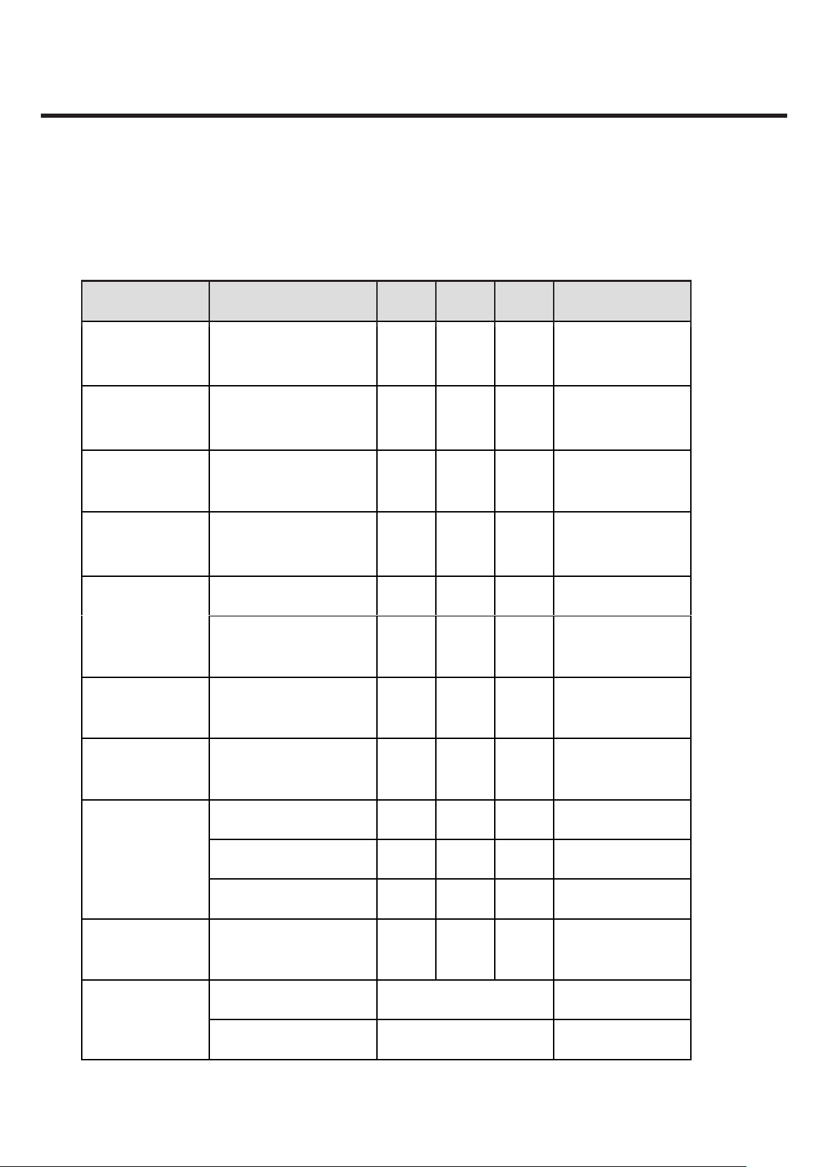
2.5 HW SPEC
LG-D285 Product SPEC
2.5 HW SPEC.
1) WCDMA transmitter specification
2. PERFORMANCE
1) WCDMA transmitter specication
Item Spec. Min Typ. Max Unit
Maximum Output
Power
Frequency
Accuracy
Minimum Output
Power
Occupied
Bandwidth
Adjacent Channel
Leakage Power
Ratio
Power class Ⅲ
Δf = 5MHz
Δf = 10MHz
21.0 23.5 25.0
- -200 - +200 Hz
- - - -50 dBm/3.84MHz
- - - 4.6 MHz
- - -33 dBm/3.84MHz
- - -43 dBm/3.84MHz
dBm/3.84MHz
Error Vector
Magnitude(EVM)
Peak Code
Domain Error
Open Loop
Output Power
Transmit Off
Power
Spectrum
Emission Mask
- - - 17
- - - 15
Ior =-106.7dBm/3.84MHz -46.7 - -28.7
Ior =-65.7dBm/3.84MHz -23.0 - -5.0
Ior =-25.0dBm/3.84MHz -0.0 - 14.0
- - - -56 dBm/3.84MHz
Δf = 2.5~3.5MHz -35-15 * (Δf-2.5) dBc/30KHz
Δf = 3.5~7.5MHz -35-1 * (Δf-3.5) dBc/1MHz
dBm/3.84MHz
dBm/3.84MHz
dBm/3.84MHz
dBm/3.84MHz
%
LGE Internal Use Only
- 11 -
Copyright © 2014 LG Electronics. Inc. All right reserved.
Only for training and service purposes
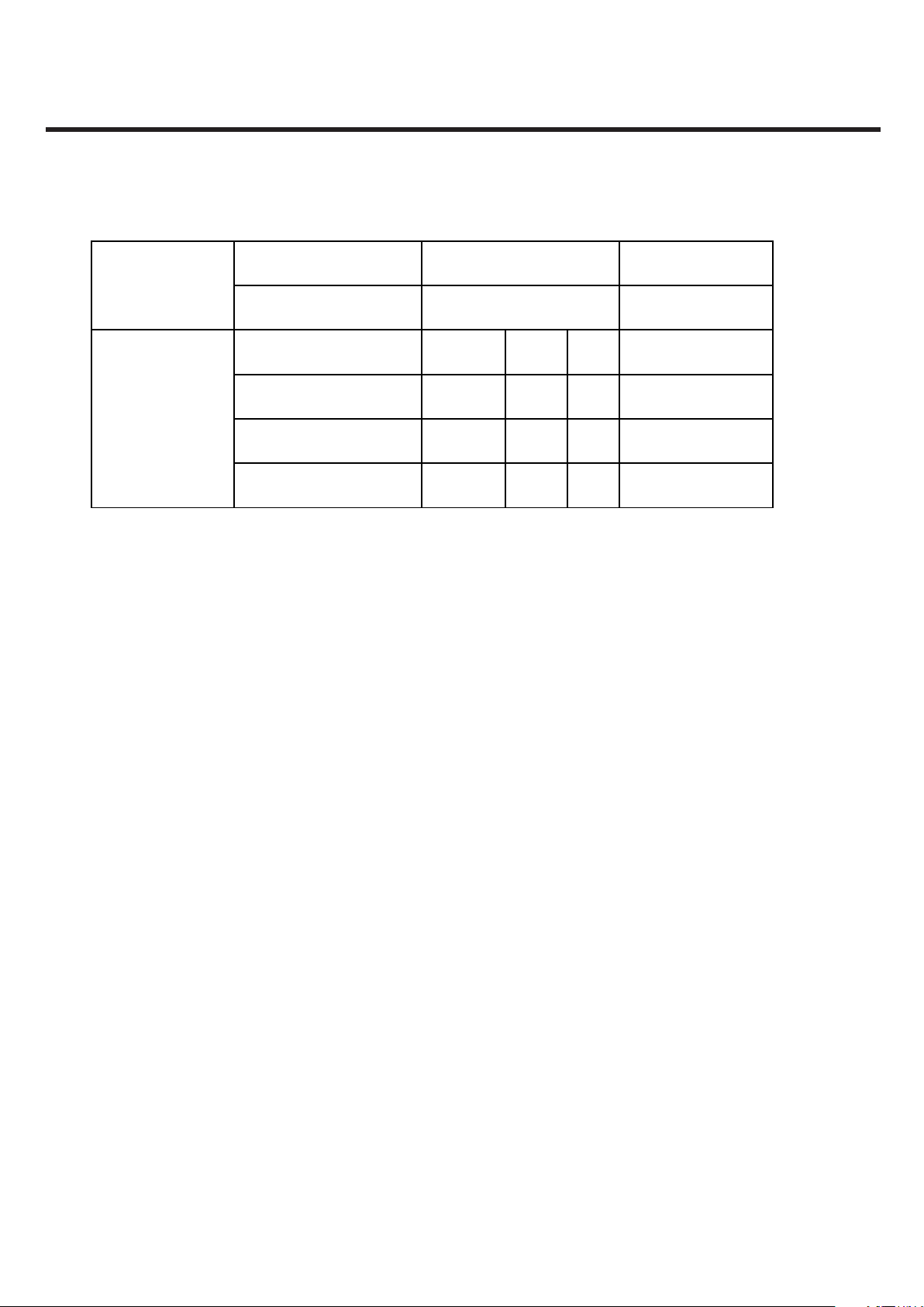
2. PERFORMANCE
LG-D285 Product SPEC
Δf = 7.5~8.5MHz -39 10 * (Δf-7.5) dBc/1MHz
Δf = 8.5~12.5MHz -49 dBc/1MHz
9kHz ~ 150kHz -36 dBm
Transmit Spurious
Emission
150kHz ~ 30MHz -36 dBm
30MHz ~ 1GHz -36 dBm
1GHz ~ 12.5GHz -30 dBm
LGE Internal Use Only
- 12 -
Copyright © 2014 LG Electronics. Inc. All right reserved.
Only for training and service purposes
2) WCDMA receiver specication
LG-D285 Product SPEC
2) WCDMA receiver specification
Item Specification
2. PERFORMANCE
BD1: 2110 ~ 2170 MHz
Receive Frequency
Reference Sensitivity Level
<REFÎ
>
or
Maximum Input Level BER < 0.001 when Îor = -25 dBm / 3.84 MHz
Adjacent Channel Selectivity
(ACS)
Blocking Characteristic
Spurious Response
BD5: 869 MHz ~ 894 MHz
BD8: 925 MHz ~ 960 MHz
Band1 : BER < 0.001 when Îor = -106.7 dBm / 3.84 MHz
Band5 : BER < 0.001 when Îor = -104.7 dBm / 3.84 MHz
Band8 : BER < 0.001 when Îor = -103.7 dBm / 3.84 MHz
ACS > 33 dB where BER < 0.001 when
Îor = <REFÎ
> + 14 dB / 3.84 MHz
or
& Ioac = –52 dBm / 3.84 MHz @ ±5 MHz
BER < 0.001 when Îor = <REFÎ
> + 3 dB / 3.84 MHz
or
& Iblocking = -56 dBm / 3.84 MHz @ Fuw(offset) = ±10 MHz
or Iblocking = -44 dBm / 3.84 MHz @ Fuw(offset) = ±15 MHz
BER < 0.001 when Îor = <REFÎ
> + 3 dB / 3.84 MHz
or
& Iblocking = -44 dBm
BER < 0.001 when Îor= <REFÎ
> + 3 dB / 3.84 MHz
or
Intermodulation
Spurious Emissions
Inner Loop Power Control
In Uplink
LGE Internal Use Only
& Iouw1 = -46 dBm @ Fuw1(offset) = ±10 MHz
& Iouw2 = -46 dBm / 3.84 MHz @ Fuw2(offset) = ±20 MHz
< -57 dBm / 100 kHz BW @ 9 kHz ≤ f < 1 GHz
< -47 dBm / 1 MHz BW @ 1 GHz ≤ f ≤ 12.75 GHz
Adjust output(TPC command)
cmd 1dB 2dB 3dB
+1 +0.5/1.5 +1/3 +1.5/4
0 -0.5/+0.5 -0.5/+0.5 -0.5/+0.5
-1 -0.5/-1.5 -1/-3 -1.5/-4
group(10equal command group)
+1 +8/+12 +16/+24
- 13 -
Copyright © 2014 LG Electronics. Inc. All right reserved.
Only for training and service purposes
2. PERFORMANCE
LG-D285 Product SPEC
3) HSDPA transmitter specification
3) HSDPA transmitter specication
Item Spec. Min Typ. Max Unit
Trands
mitter
5.2.A
Maximum
Output Power
with HS-
DPCCH
5.7A HSDPCCH
5.9A Spectrum
Emission Mask
with HS-
DPCCH
1/15 c/d 12/15
13/15 c/d 15/8
15/7 c/d 15/0
Step 0
Step 1 – Step 0
MAX /
0dBm
Step 2 – Step 3
Step 5 – Step 4
Step 6 – Step 7
Δf = 2.5~3.5MHz -35-15 * (Δf-2.5) dBc/30KHz
Δf = 3.5~7.5MHz -35-1 * (Δf-3.5) dBc/1MHz
Δf = 7.5~8.5MHz -39 10 * (Δf-7.5) dBc/1MHz
21.0
20
19
22.5
22.5
22
0 dBm +/- 1 dB dB
6 dB +/- 2.3 dB dB
1 dB +/- 0.6 dB dB
0 dB +/- 0.6 dB dB
5 dB +/- 2.3 dB dB
25.0
25
25
dBm/3.84MHz
5.10A Adjacent
Leakage Power
(EVM) with HS-
6.3A Maximum
Receiver
LGE Internal Use Only
Input Level for
Channel
Ratio with HS-
DPCCH
5.13.1A Error
Vector
Magnitude
DPCCH
HS-PDSCH
Reception
Δf = 8.5~12.5MHz -49 dBc/1MHz
Δf = 5MHz
Δf = 10MHz
MAX Power
-20 dBm
Pin = -25dBm - - 10 BLER(%)
- 14 -
- - -33 dBm/3.84MHz
- - -43 dBm/3.84MHz
- - 17.5
Copyright © 2014 LG Electronics. Inc. All right reserved.
Only for training and service purposes
%
LG-D285 Product SPEC
4) GSM receiver specification
/
4) GSM receiver specication
2. PERFORMANCE
Item Spec.
EMC(Radiated Spurious Emission
Transmitter Output power and Burst Timing
Spectrum due to modulation out to less
Spectrum due to modulation out to larger
than 1800kHz offset to the edge of the
Phase Error Rms : 5°
Frequency Error
Disturbance)
Burst Timing <3.69us
than 1800kHz offset
transmit band
Peak : 20 °
GSM : 0.1 ppm
DCS/PCS : 0.1 ppm
3000kHz-6000kHz : <-65dBc(-46dBm)
GSM/DCS : < -28dBm
GSM : 5dBm – 33dBm ± 3dB
DCS/PCS : 0dBm – 30dBm ± 3dB
200kHz : -36dBm
600kHz : -51dBm/-56dBm
GSM :
1800-3000kHz :< -63dBc(-46dBm)
6000kHz < : < -71dBc(-46dBm)
DCS :
Spectrum due to switching transient
Reference Sensitivity – TCH/FS Class II(RBER) : -105dBm(2.439%)
Usable receiver input level range 0.012(-15 - -40dBm)
Intermodulation rejection – Speech
channels
AM Suppression
- GSM : -31dBm - DCS : -29dBm
Timing Advance ± 0.5T
LGE Internal Use Only
1800-3000kHz :< -65dBc(-51dBm)
6000kHz < : < -73dBc(-51dBm)
400kHz : -19dBm/-22dBm(5/0), -23dBm
600kHz : -21dBm/-24dBm(5/0), -26dBm
- 15 -
± 800kHz, ± 1600kHz
: -98dBm/-96dBm (2.439%)
-98dBm/-96dBm (2.439%)
Copyright © 2014 LG Electronics. Inc. All right reserved.
Only for training and service purposes
LG-D285 Product SPEC
5) Bluetooth transmitter specification
5) Bluetooth transmitter specication
2. PERFORMANCE
Tx Output Spectrum
Tx Output Spectrum
Item Spec. Min Typ. Max
Output Power
Power Density
Power Control
Frequency Range
DH5
PRBS9
DH5
PRBS9
DH1
PRBS9
DH5
PRBS9
DH5
(20dB BW)
(Adjacent Output
Power)
PRBS9
DH5
PRBS9
Power
(Class I)
@100kHz
RBW
Step size
Power(min)
0 - +20
- +20
2 - 8 dB
- 4 dBm
-30dBc
@100kHz
2400 - 2483.5 MHz
RBW
H-fL
- 1 MHz
Δf =f
@M-N = 2 - -20
@M-N 3
- -40
Unit
dBm
dBm
dBm
dBm
Modulation Index
Initial Carrier Freq.
Tolerance
Carrier Frequency Drift
DH5
11110000
DH5
10101010
f2
DH5
PRBS9
DH1
Freq. Drift -25 - +25
10101010
Drift Rate -20 - +20
Freq. Drift -40 - +40
DH3
10101010
Drift Rate -20 - +20
Freq. Drift -40 - +40
DH5
10101010
Drift Rate -20 - +20
AVG
f1
f2
AVG
MAX
/f1
AVG
140 - 175
115 -
0.8 -
-75 - +75
kHz
kHz
kHz
kHz
kHz/50us
kHz
kHz/50us
kHz
kHz/50us
LGE Internal Use Only
- 16 -
Copyright © 2014 LG Electronics. Inc. All right reserved.
Only for training and service purposes

LG-D285 Product SPEC
6) Bluetooth receiver specification
6) Bluetooth receiver specication
2. PERFORMANCE
Item
Sensitivity
(Single Slot Packet)
Sensitivity
(Multi Slot Packet)
C/I Performance*
Input power @BT_w
Input power @BT_w
Input power @BT_i
DH1
PRBS9
DH5
PRBS9
DH1
PRBS9
Spec.
BER=0.1%
C/I@Co-Channel
C/I @ Image1MHz
-
-
-60dBm @ BT
C/I @1MHz
-60dBm@ BT
C/I @2MHz
-60dBm@ BT
C/I @≥3MHz
-67dBm@ BT
C/I @Image
-67dBm@ BT
-67dBm@ BT
Min Typ. Max Unit
- -70 dBm
- -70 dBm
- 11
- 0
- -30
dB
- -40
- -9
- -20
Blocking Performance
Intermodulation
Performance
Maximum Input Level
DH1
PRBS9
Input power @CW
DH1
PRBS9
Input power @CW_i
DH1
PRBS9
Input power @BT_w
30M ~2 GHz
-67dBm@ BT
2 ~ 2.4 GHz
-67dBm@ BT
2.5 ~ 3 GHz
-67dBm@ BT
3 ~ 12.75 GHz
-67dBm@ BT
Δf = +5MHz (CW_i)
Δf = +10MHz (BT_i)
-64dBm@ BT_w
Δf = -5MHz (CW_i)
Δf = -10MHz (BT_i)
-64dBm@ BT_w
- -20 -
-10 -
-27 -
-27 -
-10 -
-39 -
-39 -
dBm
dBm
dBm
dBm
LGE Internal Use Only
- 17 -
Copyright © 2014 LG Electronics. Inc. All right reserved.
Only for training and service purposes
LG-D285 Product SPEC
7) WLAN 802.11b transceiver specification
7) WLAN 802.11b transceiver specication
Item Specification
2. PERFORMANCE
Transmit Frequency 2400 MHz ~ 2483.5 MHz ( CH1~CH13)
Tx Power Level
Frequency Tolerance within ±25 PPM
Chip clock Frequency
Tolerance
≤ -30 @ fc-22MHz< f <fc-11MHz and fc+11MHz< f <fc+22MHz
Spectrum Mask
Power ramp on/off time
Carrier Suppression
Modulation Accuracy
(Peak EVM)
≤ 20dBm under (Europe), ≤ 30dBm under (USA)
within ±25 PPM
≤ -50 @ f < fc-22MHz and f > fc+22MHz
≤ 2us
≤ -15dB
≤ 35%
Spurious Emissions
Rx Min input Sensitivity
Rx Max input Sensitivity
Rx Adjacent Channel
Rejection
LGE Internal Use Only
< -36 dBm @ 30MHz ~ 1GHz
< -30 dBm above @ 1GHz ~ 12.75GHz
< -47 dBm @ 1.8GHz ~ 1.9GHz
< -47 dBm @ 5.15GHz ~ 5.3GHz
≤ -76dBm(1Mbps,2Mbps,5.5Mbps,11Mbps) @ FER ≤ 8%
≥ -10dBm(1Mbps,2Mbps,5.5Mbps,11Mbps) @ FER ≤ 8%
≥ 35dB @FER ≤ 8%,
interference input signal -70dBm@fc±25MHz(11Mbps)
- 18 -
Copyright © 2014 LG Electronics. Inc. All right reserved.
Only for training and service purposes
2. PERFORMANCE
LG-D285 Product SPEC
8) WLAN 802.11g transceiver specification
8) WLAN 802.11g transceiver specication
Item Specification
Transmit Frequency 2400 MHz ~ 2483.5 MHz ( CH1~CH13)
Tx Power Level
Frequency Tolerance within ±25 PPM
Chip clock Frequency
Tolerance
Spectrum Mask
Transmitter constellation error
(rms EVM)
≤ 20dBm under (Europe), ≤ 30dBm under (USA)
within ±25 PPM
≤ -20 @ ±11MHz offset (9Mhz ~ 11MHz)
≤ -28 @ ±20MHz offset (11MHz ~ 20Mhz)
≤ -40 @ ±30MHz offset (20MHz ~ 30Mhz)
≤ -5dB
Spurious Emissions
Rx Min input Sensitivity
Rx Max input Sensitivity
Rx Adjacent Channel
Rejection
< -36 dBm @ 30MHz ~ 1GHz
< -30 dBm above @ 1GHz ~ 12.75GHz
< -47 dBm @ 1.8GHz ~ 1.9GHz
< -47 dBm @ 5.15GHz ~ 5.3GHz
PER ≤ 10%
-82dBm@6Mbps, -81dBm@9Mbps, -79dBm@12Mbps
-77dBm@18Mbps, -74dBm@24Mbps, -70dBm@36Mbps
-66dBm@48Mbps, -65dBm@54Mbps
≥ -20dBm(6,9,12,18,24,36,48,54Mbps) @ PER ≤ 10%
PER ≤ 10%,
ACR ≥ 16dB@6Mbps, ACR ≥ 15dB@9Mbps,
ACR ≥ 13dB@12Mbps, ACR ≥ 11dB@18Mbps,
ACR ≥ 8dB@24Mbps, ACR ≥ 4dB@36Mbps
ACR ≥ 0dB@48Mbps, ACR ≥ -1dB@54Mbps
※ACR shall be measured by setting the desired signal's
LGE Internal Use Only
strength 3 dB above the rate-dependent
sensitivity specified in min input sensitivity
- 19 -
Copyright © 2014 LG Electronics. Inc. All right reserved.
Only for training and service purposes
LG-D285 Product SPEC
9) WLAN 802.11n transceiver specification
9) WLAN 802.11n transceiver specication
2. PERFORMANCE
Transmit Frequency
Item Specification
Tx Power Level ≤ 20dBm under (Europe), ≤ 30dBm under (USA)
Frequency Tolerance within ±25 PPM
Chip clock Frequency Tolerance within ±25 PPM
Spectrum Mask ≤ -20 @ ±11MHz offset (9Mhz ~ 11MHz)
Transmitter constellation error
(rms EVM)
Spurious Emissions < -36 dBm @ 30MHz ~ 1GHz
2400 MHz ~ 2483.5 MHz ( CH1~CH13)
≤ -28 @ ±20MHz offset (11MHz ~ 20Mhz)
≤ -45 @ ±30MHz offset (20MHz ~ 30Mhz)
≤ -5dB@6.5Mbps, ≤ -10dB@13Mbps, ≤ -13dB@19.5Mbps,
≤ -16dB@26Mbps, ≤ -19dB@39Mbps, ≤ -22dB@52Mbps,
≤ -25dB@58.5Mbps, ≤ -28dB@65Mbps
< -30 dBm above @ 1GHz ~ 12.75GHz
< -47 dBm @ 1.8GHz ~ 1.9GHz
< -47 dBm @ 5.15GHz ~ 5.3GHz
Rx Min input Sensitivity PER ≤ 10%
-82dBm@6.5Mbps, -79dBm@13Mbps, -77dBm@19.5Mbps
-74dBm@26Mbps, -70dBm@39Mbps, -66dBm@52Mbps
-65dBm@58.5Mbps, -64dBm@65Mbps
Rx Max input Sensitivity ≥ -20dBm(6.5,13,19.5,26,39,52,58.5,65Mbps) @ PER ≤ 10%
Rx Adjacent Channel
Rejection
ACR ≥ 16dB@6.5Mbps, ACR ≥ 13dB@13Mbps,
ACR ≥ 11dB@19.5Mbps, ACR ≥ 8dB@26Mbps,
ACR ≥ 4dB@39Mbps, ACR ≥ 0dB@52Mbps
ACR ≥ -1dB@58.5Mbps, ACR ≥ -2dB@65Mbps
※ACR shall be measured by setting the desired signal's strength
3 dB above the rate-dependent
sensitivity specified in min input sensitivity
PER ≤ 10%,
LGE Internal Use Only
- 20 -
Copyright © 2014 LG Electronics. Inc. All right reserved.
Only for training and service purposes
10) GPS receiver specication
LG-D285 Product SPEC
10) GPS receiver specification
LG-D285 Product SPEC
10) GPS receiver specification
Item Spec.
Sensitivity Test
Success rate ≥ 60% @ -154 dBm
11) Current consumption
** Test condition for Standby current consumption should be as below.
: Measurement time 1hr, with Agilent & CMT JIG
Item Spec.
2. PERFORMANCE
Sensitivity Test
11) Current consumption
** Test condition for Standby current consumption should be as below.
: Measurement time 1hr, with Agilent & CMT JIG
Item
1. Sleep Mode Under 3.5mA Under 3.5mA
2. Sleep : connector Ear jack Under 4.5mA Under 4.5mA
WCDMA GSM
Success rate ≥ 60% @ -154 dBm
Specification
3. Current(Sleep & Idle AVG) Under 4.5mA @ DRX 7 Under 4.5mA @ P.P 5
4. BT Connected idle Under 6mA Under 6mA
5. Talk Mode
6. No SVC Mode under 200mA Under 200 mA
7. Power Off Mode under 300uA Under 300 uA
LGE Internal Use Only
- Max Pwr
Under 600mA @ Avg
- Tx 10dBm
Under 400 mA @ Avg
- 21 -
GSM LVL 5
under 400 mA @ Avg
Copyright © 2014 LG Electronics. Inc. All right reserved.
Only for training and service purposes
LG-D285 Product SPEC
12) RSSI indicator (Based on Cell power)
BAR GSM/DCS/PCS WCDMA
54
-89±2dBm
-91±2dBm
43
-94±2dBm
-96±2dBm
32
-100±2dBm
-99±2dBm
21
-104±2dBm
-103±2dBm
10
-110±2dBm
-105±2dBm
13) Current consumption
LG-D285 Product SPEC
12) RSSI indicator (Based on Cell power)
BAR GSM/DCS/PCS WCDMA
54
-89±2dBm
-91±2dBm
43
-94±2dBm
-96±2dBm
32
-100±2dBm
-99±2dBm
21
-104±2dBm
-103±2dBm
10
-110±2dBm
-105±2dBm
13) Current consumption
Standby
(WCDMA)
Over 466 Hours
Under 4.5mA
DRX 7 @ BATT Capacity : 2100mAh
14) Charging hour
Under 4 hour (2100mAh battery, 700mA TA)
12) RSSI indicator (Based on Cell power)
LG-D285 Product SPEC
12) RSSI indicator (Based on Cell power)
2. PERFORMANCE
BAR GSM/DCS/PCS WCDMA
13) Current consumption
54
43
32
21
10
Standby
(WCDMA)
Over 466 Hours
Under 4.5mA
WCDMA GSM/DCS/PCS
-89±2dBm
-94±2dBm
-100±2dBm
-104±2dBm
-110±2dBm
DRX 7 @ BATT Capacity : 2100mAh
14) Charging hour
-91±2dBm
-96±2dBm
-99±2dBm
-103±2dBm
-105±2dBm
Under 4 hour (2100mAh battery, 700mA TA)
LGE Internal Use Only
- 22 -
Copyright © 2014 LG Electronics. Inc. All right reserved.
Only for training and service purposes
15) Battery indicator
2. PERFORMANCE
Battery Bar Specication Battery Bar Specication
BAR 20 (Full) 98% over BAR 9 --> 8 43% -> 42%
BAR 20 --> 19 98% -> 97% BAR 8 --> 7 38% -> 37%
BAR 19 --> 18 93% -> 92% BAR 7 --> 6 33% -> 32%
BAR 18 --> 17 88% -> 87% BAR 6 --> 5 28% -> 27%
BAR 17 --> 16 83% -> 82% BAR 5 --> 4 23% -> 22%
BAR 16 --> 15 78% -> 77% BAR 4 --> 3 18% -> 17%
BAR 15 --> 14 73% -> 72% BAR 3 --> 2 13% -> 12%
BAR 14 --> 13 68% -> 67% BAR 2 --> 1 8% -> 7%
BAR 13 --> 12 63% -> 62% BAR 1 --> 0 3% -> 2%
BAR 12 --> 11 58% -> 57% Power o 1%
BAR 11 --> 10 53% -> 52% Low Battery Pop-up 15%, 5%, 0%
BAR 10 --> 9 48% -> 47%
LGE Internal Use Only
- 23 -
Copyright © 2014 LG Electronics. Inc. All right reserved.
Only for training and service purposes
LG-D285 Product SPEC
2.6 D285 Figures
2.6 D285F Figures
2. PERFORMANCE
LGE Internal Use Only
- 24 -
Copyright © 2014 LG Electronics. Inc. All right reserved.
Only for training and service purposes
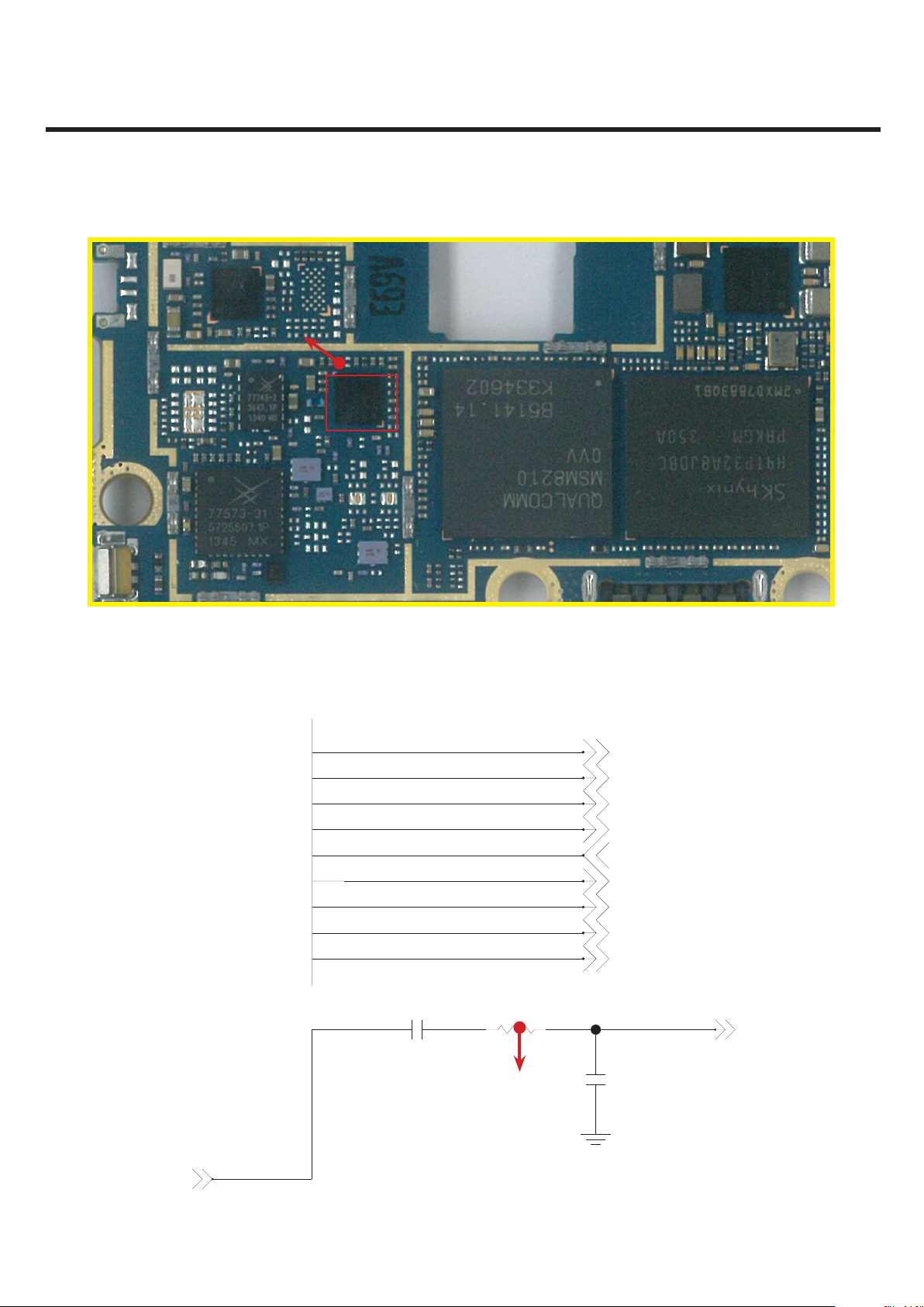
3. TROUBLE SHOOTING
3.1 WCDMA Rx Part
3.1.1 WCDMA_B1 Rx
3. TROUBLE SHOOTING
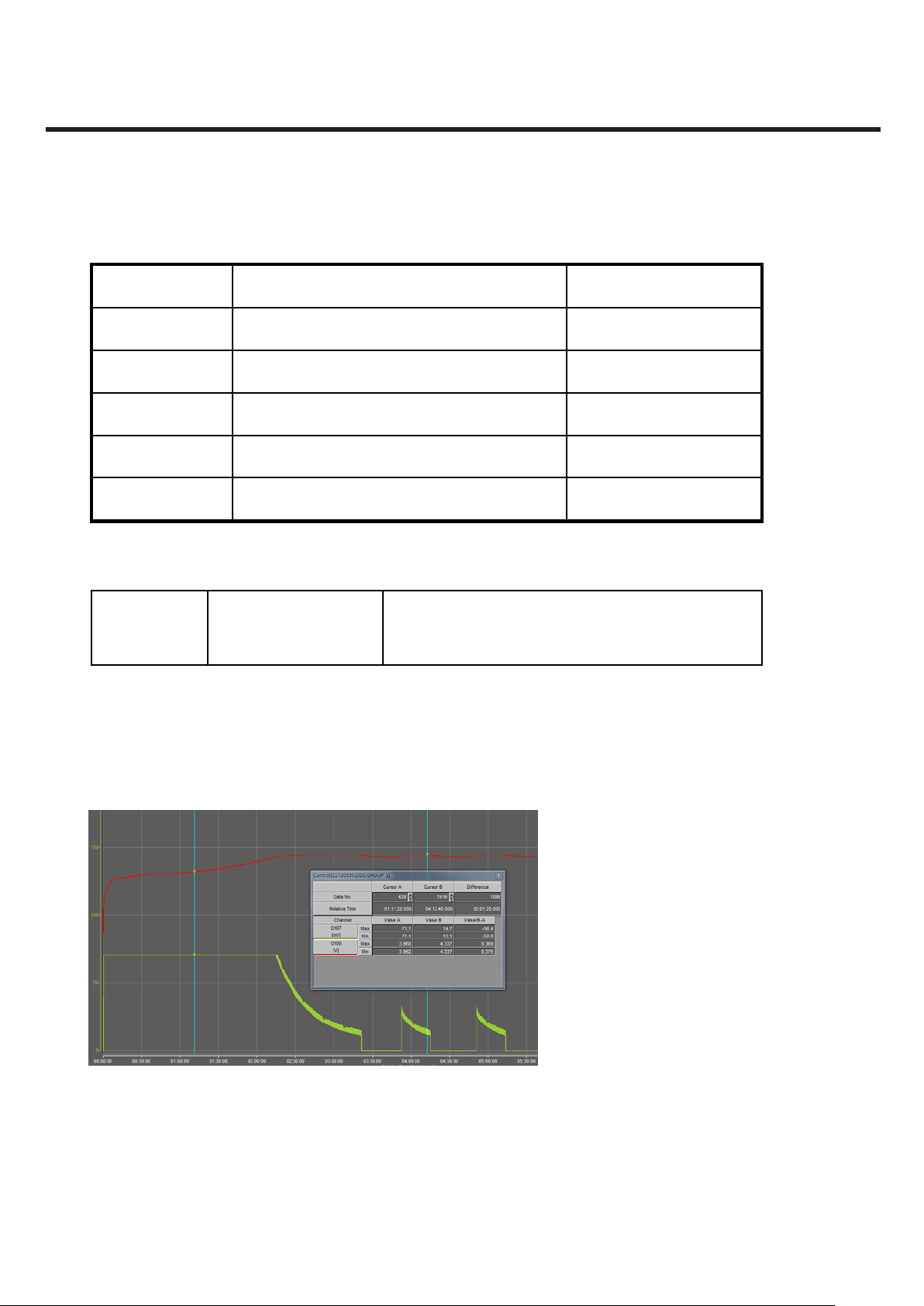
START
Rx TEST SETUP
- DL Channel : 10700
- Sector Power : -30 dBm
1. Check
DC Power Supply circuit
2. Check WTR2605 XO
3.Check RF Signal path
Re download S/W & Cal
※ there are no Test Points on the IQ Data Line. So It is impossible to check the IQ Data Wave form
LGE Internal Use Only
- 25 -
Copyright © 2014 LG Electronics. Inc. All right reserved.
Only for training and service purposes
WTR2605
(U3000)
3. TROUBLE SHOOTING
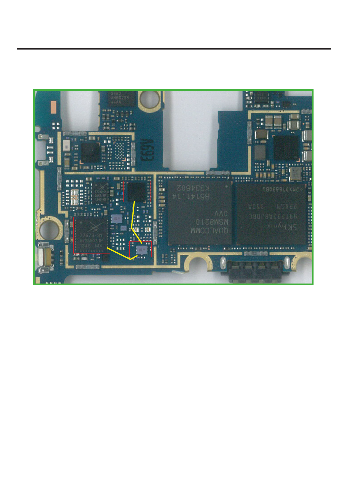
SKY7757331 (U1000)
DPX
(FL2001)
<Main Top>
LGE Internal Use Only
- 26 -
Copyright © 2014 LG Electronics. Inc. All right reserved.
Only for training and service purposes
3.1.1.1 Checking DC Power supply circuit
START
3. TROUBLE SHOOTING
Check TP1(C3001)
+2V05_VREG_L9 is OK?
Yes
Check TP2(C3007)
+1V225_VREG_L1 is OK?
Yes
Check TP3(C3016)
+1V8_VREG_L10 is OK?
Yes
DC Power Supply Circuit is OK
See Next page to Check XO Circuit
No
No
No
The Problem may be Logic part
Refer to Logic troubleshoot
The Problem may be Logic part
Refer to Logic troubleshoot
The Problem may be Logic part
Refer to Logic troubleshoot
LGE Internal Use Only
- 27 -
Copyright © 2014 LG Electronics. Inc. All right reserved.
Only for training and service purposes
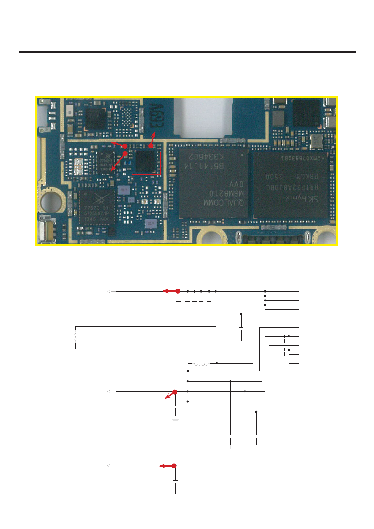
TP1 : C3001
(+2V05_VREG_L9)
TP2: C3007
(+1V225_VREG_L1)
3. TROUBLE SHOOTING
TP3: C3016
(+1V8_VREG_L10)
WTR2605
(U3000)
+2V05_VREG_L9
Tuning point (Inductor Placeholder)
0
R3007
+1V225_VREG_L1
TP2
TP1
<Main Top>
C3001 4.7u
C3002 0.1u
C3003 0.1u
C3007
4.7u
0.1uC3004
0.1uF STAR ROUTE
C3005 0.1u
C3006
0.1u
10nL3001
0.1uC3010
0.1uC3009
0.1uC3011
STAR ROUTE
0.1uC3012
19
VDD_RF2_R_BB
16
VDD_RF2_T_DA
37
VDD_RF2_T_VCO
52
VDD_RF2_T_PLL
40
VDD_RF2_R_PLL
54
VDD_RF2_XO
39
VDD_RF1_R_VCO
46
VDD_RF1_T_PLL
26
VDD_RF1_T_LO
30
VDD_RF1_R_LO
20
VDD_RF1_LNA
48
VDD_RF1_DIG
31
VDD_RF1_G_LO
21
VDD_RF1_G_PLL
59
VDD_RF3_IO
U3000
+1V8_VREG_L10
LGE Internal Use Only
TP3
C3016 0.1u
- 28 -
Copyright © 2014 LG Electronics. Inc. All right reserved.
Only for training and service purposes
3.1.1.2 Checking WTR2605 XO circuit
START
3. TROUBLE SHOOTING
Check TP1(R3005)
Is it 19.2MHz?
NO
Replace X4100 and then check
TP1(R3005)
Is it similar ?
NO
Replace Main B/D
YES
YES
XO circuit is Ok . See next page
to check RF signal path.
XO circuit is Ok . See next page
to check RF signal path.
LGE Internal Use Only
- 29 -
Copyright © 2014 LG Electronics. Inc. All right reserved.
Only for training and service purposes
TP1 : R3005
(WTR_XO_IN)
3. TROUBLE SHOOTING
WTR2605
(U3000)
U3000
RX_BB_IP
RX_BB_IM
RX_BB_QP
RX_BB_QM
XO_IN
GNSS_BB_IP
GNSS_BB_IM
GNSS_BB_QP
GNSS_BB_QM
61
55
49
43
60
62
51
45
41
<Main Top>
100pC3008 R3005 0
TP1
WTR0_PRXBB_I_P
WTR0_PRXBB_I_N
WTR0_PRXBB_Q_P
WTR0_PRXBB_Q_N
WTR_XO_IN
WTR0_GNSSBB_I_P
WTR0_GNSSBB_I_N
WTR0_GNSSBB_Q_P
WTR0_GNSSBB_Q_N
WTR_XO_IN
C3013
DNI
WTR0_XO_IN
LGE Internal Use Only
- 30 -
Copyright © 2014 LG Electronics. Inc. All right reserved.
Only for training and service purposes

3.1.1.3 Checking RF signal path (TX Module)
START
3. TROUBLE SHOOTING
Check TP1(C1002) at U1000
Check if there is any major dierence referring
To Figure 3.1.1(b). Is any signal detected at that
point?
Yes
Check TP2(C2038) at FL2001
Check if there is any major dierence referring
To Figure 3.1.1(c). Is any signal detected at that
point?
Yes
Is any signal detected at
that point?
No
No
No
Check L1001,C1001, L1000, SW1001
Check TP3(C1023),TP4(C1024),TP5(C1019),
TP6(C1020) at U1000. Is any DC signal detected
at that points?
Yes
Replace U1000
Check C2038
No
TX module is OK. See next page to check DPX
LGE Internal Use Only
Yes
The Problem may be Logic part
Refer to Logic troubleshoot
- 31 -
Copyright © 2014 LG Electronics. Inc. All right reserved.
Only for training and service purposes

TP5
3. TROUBLE SHOOTING
TP4
TP6
SW1000
G1
SKY77573-31
TP1
ANTG2
(U1000)
TP3
TP2
<Main Top>
1nC1000
SW1001
ANT COMMON
G3 G4
43
21
C1001 3.3n
L1000
27n
L1001
0.5p
C1002
1n
TP1
LGE Internal Use Only
- 32 -
Copyright © 2014 LG Electronics. Inc. All right reserved.
Only for training and service purposes

3. TROUBLE SHOOTING
Boost Option
+VPWR_BOOST_BYP
GND15
22
GND16
23
C1013
4.7u
TRX1
24
GND17
25
TRX2
26
GND18
27
TRX3
28
GND19
29
TRX4
30
GND20
31
VBATT
32
NC1
33
TX_MODULE_TRX_1
TX_MODULE_TRX_2
TX_MODULE_TRX_4
C1112
22p
TP3
ANT0_SW_SEL_0
DNI
R1006
SPDT_SEL
C1113
100p
100p
C1023
C1024
100p
100p
R1004
WTR_TX1_OUT PA0_R_0
C1060
0
DNI
R1005
21
20
RX2
SPDT_OUT
SKY77573-31
NC2
34
TP4
19
18
RX1
SPDT_IN
U1000
RF_IN36SPDT35SW038SW1
37
TP5
16
GND1417GND13
HB_EN
39
13
14
15
ANT
GND12
GND11
GND10
GND9
GND8
GND7
GND6
GND5
GND4
VCC2
VCC1
GND3
GND2
GND1
LB_EN40MODE041MODE142PGND
43
TP6
C1019 100p
100p
C1020
12
11
10
9
8
7
6
5
4
3
2
1
C1015
100p
Boost Option
C1017
C1016
10n
4.7u
PA0_R_1
ANT0_SW_SEL_3
ANT0_SW_SEL_2ANT0_SW_SEL_1
100p
100p
C1022
C1021
W-BAND DPX
B1
B2
EAM62692801(B5897)
EAM62890101(B8613)
TRX B1
FL2001
ANT
GND1 GND6
GND2 GND5
GND3 GND4
16
RX
3
TX
92
84
75
TX_MODULE_TRX_1
TP2
4.7pC2038
L2003
2p
3nC2039
L2010
DNI
+VPWR_BOOST_BYP
B1
C2037
100p
L2011
DNI
LGE Internal Use Only
- 33 -
Copyright © 2014 LG Electronics. Inc. All right reserved.
Only for training and service purposes

Figure 3.1.1 (b) TP1
2.140GHz
2.140GHz
3. TROUBLE SHOOTING
LGE Internal Use Only
Figure 3.1.1 (c) TP2
- 34 -
Copyright © 2014 LG Electronics. Inc. All right reserved.
Only for training and service purposes

3.1.1.4 Checking RF signal path(Duplexer)
START
3. TROUBLE SHOOTING
Check TP1(C2062) at FL2001
Check if there is any major dierence referring
To Figure 3.1.1(b) Is any signal detected at
that point?
Yes
Is any signal detected at that point?
Yes
All WCDMA_B1 Rx check is complete.
If the phone sill do not work ,replace main board
No
No
Check C2037, C2062, C2027, C2028
Replace FL2001
LGE Internal Use Only
- 35 -
Copyright © 2014 LG Electronics. Inc. All right reserved.
Only for training and service purposes

TP1
3. TROUBLE SHOOTING
LNA_PRX_MB1_IN
C2062
TP1
FL2001 DPX
<Main Top>
2.7n
L2002
C2028
DNI
C2030
DNI
33p
C2027
33p
B1
WTR_PRX_MB_1_IN
LGE Internal Use Only
- 36 -
Copyright © 2014 LG Electronics. Inc. All right reserved.
Only for training and service purposes

Figure 3.1.1 (b)
2.140GHz
3. TROUBLE SHOOTING
LGE Internal Use Only
- 37 -
Copyright © 2014 LG Electronics. Inc. All right reserved.
Only for training and service purposes

3.1.2 WCDMA_B5 Rx
3. TROUBLE SHOOTING
START
Rx TEST SETUP
- Test Channel : 4407
- Sector Power : -30 dBm
1. Check
DC Power Supply circuit
2. Check WTR2605 XO
3. Check RF Signal Path
Re download S/W, Cal
* There are no Test Points on the IQ Data Line. So It is impossible to check the IQ Data Wave form.
LGE Internal Use Only
- 38 -
Copyright © 2014 LG Electronics. Inc. All right reserved.
Only for training and service purposes

WTR2605
(U3000)
3. TROUBLE SHOOTING
SKY7757331 (U1000)
DPX
(FL2002)
<Main Top>
LGE Internal Use Only
- 39 -
Copyright © 2014 LG Electronics. Inc. All right reserved.
Only for training and service purposes

3.1.2.1 Checking DC Power supply circuit
START
3. TROUBLE SHOOTING
Check TP1(C3001)
+2V05_VREG_L9 is OK?
Yes
Check TP2(C3007)
+1V225_VREG_L1 is OK?
Yes
Check TP3(C3016)
+1V8_VREG_L10 is OK?
Yes
No
The Problem may be Logic part
Refer to Logic troubleshoot
No
The Problem may be Logic part
Refer to Logic troubleshoot
No
The Problem may be Logic part
Refer to Logic troubleshoot
DC Po wer su pply Circuit is OK. See next
LGE Internal Use Only
Page to check XO circuit
- 40 -
Copyright © 2014 LG Electronics. Inc. All right reserved.
Only for training and service purposes

TP1 : C3001
(+2V05_VREG_L9)
TP2: C3007
(+1V225_VREG_L1)
3. TROUBLE SHOOTING
TP3: C3016
(+1V8_VREG_L10)
WTR2605
(U3000)
+2V05_VREG_L9
Tuning point (Inductor Placeholder)
0
R3007
+1V225_VREG_L1
TP2
TP1
<Main Top>
C3001 4.7u
C3002 0.1u
C3003 0.1u
C3007
4.7u
0.1uC3004
0.1uF STAR ROUTE
C3005 0.1u
C3006
0.1u
10nL3001
0.1uC3010
0.1uC3009
0.1uC3011
STAR ROUTE
0.1uC3012
19
VDD_RF2_R_BB
16
VDD_RF2_T_DA
37
VDD_RF2_T_VCO
52
VDD_RF2_T_PLL
40
VDD_RF2_R_PLL
54
VDD_RF2_XO
39
VDD_RF1_R_VCO
46
VDD_RF1_T_PLL
26
VDD_RF1_T_LO
30
VDD_RF1_R_LO
20
VDD_RF1_LNA
48
VDD_RF1_DIG
31
VDD_RF1_G_LO
21
VDD_RF1_G_PLL
59
VDD_RF3_IO
U3000
+1V8_VREG_L10
LGE Internal Use Only
TP3
C3016 0.1u
- 41 -
Copyright © 2014 LG Electronics. Inc. All right reserved.
Only for training and service purposes

3.1.2.2 Checking MT6162 XO circuit
START
3. TROUBLE SHOOTING
Check TP1(R3005)
Is it 19.2MHz?
No
Replace X4100 and then check
TP1(R3005)
Is it similar ?
No
Replace Main B/D
Yes
Yes
XO circuit is Ok. See next page
to check RF signal path
XO circuit is Ok. See next page
to check RF signal path.
LGE Internal Use Only
- 42 -
Copyright © 2014 LG Electronics. Inc. All right reserved.
Only for training and service purposes

TP1 : R3005
(WTR_XO_IN)
3. TROUBLE SHOOTING
WTR2605
(U3000)
U3000
RX_BB_IP
RX_BB_IM
RX_BB_QP
RX_BB_QM
XO_IN
GNSS_BB_IP
GNSS_BB_IM
GNSS_BB_QP
GNSS_BB_QM
61
55
49
43
60
62
51
45
41
<Main Top>
100pC3008 R3005 0
TP1
WTR0_PRXBB_I_P
WTR0_PRXBB_I_N
WTR0_PRXBB_Q_P
WTR0_PRXBB_Q_N
WTR_XO_IN
WTR0_GNSSBB_I_P
WTR0_GNSSBB_I_N
WTR0_GNSSBB_Q_P
WTR0_GNSSBB_Q_N
WTR_XO_IN
C3013
DNI
WTR0_XO_IN
LGE Internal Use Only
- 43 -
Copyright © 2014 LG Electronics. Inc. All right reserved.
Only for training and service purposes

3.1.2.3 Checking RF signal path (Tx Module)
START
3. TROUBLE SHOOTING
Check TP1(C1002) at U1000
Check if there is any major dierence referring
To Figure 3.1.1(b). Is any signal detected at that
point?
Yes
Check TP2(C2050) at FL2002
Check if there is any major dierence referring
To Figure 3.1.1(c). Is any signal detected at that
point?
Yes
Is any signal detected at that point?
No
No
No
Check L1001,C1001, L1000, SW1001
Check TP3(C1023),TP4(C1024),TP5(C1019),
TP6(C1020) at U1000. Is any DC signal detected
at that points?
Yes
Replace U1000
Check C2050
No
TX module is OK. See next page to check DPX
LGE Internal Use Only
Yes
The Problem may be Logic part
Refer to Logic troubleshoot
- 44 -
Copyright © 2014 LG Electronics. Inc. All right reserved.
Only for training and service purposes

TP5
3. TROUBLE SHOOTING
TP4
TP6
SW1000
G1
SKY77573-31
TP1
ANTG2
(U1000)
TP3
TP2
<Main Top>
1nC1000
SW1001
ANT COMMON
G3 G4
43
21
C1001 3.3n
L1000
27n
L1001
0.5p
C1002
1n
TP1
LGE Internal Use Only
- 45 -
Copyright © 2014 LG Electronics. Inc. All right reserved.
Only for training and service purposes

3. TROUBLE SHOOTING
Boost Option
+VPWR_BOOST_BYP
GND15
22
GND16
23
C1013
4.7u
TRX1
24
GND17
25
TRX2
26
GND18
27
TRX3
28
GND19
29
TRX4
30
GND20
31
VBATT
32
NC1
33
TX_MODULE_TRX_1
TX_MODULE_TRX_2
TX_MODULE_TRX_4
C1112
22p
TP3
ANT0_SW_SEL_0
DNI
R1006
TP2
SPDT_SEL
L2004
6.8n
C1113
100p
C1023
100p
C1024
100p
FL2002
6
ANT
GND12GND6
GND24GND5
GND35GND4
100p
R1004
WTR_TX1_OUT PA0_R_0
C1060
0
DNI
R1005
TX_MODULE_TRX_4 WTR_PRX_LB_1_IN
21
20
RX2
SPDT_OUT
SKY77573-31
NC2
34
TP4
19
RX1
SPDT_IN
U1000
RF_IN36SPDT35SW038SW1
TP5
RX
TX
18
GND1417GND13
37
1
3
9
8
7
14
15
16
ANT
GND12
LB_EN40MODE041MODE142PGND
HB_EN
39
13
GND11
GND10
TP6
C1019 100p
GND9
GND8
GND7
GND6
GND5
GND4
VCC2
VCC1
GND3
GND2
GND1
43
100p
C1020
12
11
10
9
8
7
6
5
4
3
2
1
C1015
100p
Boost Option
C1017
C1016
10n
4.7u
+VPWR_BOOST_BYP
PA0_R_1
ANT0_SW_SEL_3
ANT0_SW_SEL_2ANT0_SW_SEL_1
100p
100p
C1022
C1021
100pC2052C2051 100p100pC2050
C2053 18n
L2007
DNI
LGE Internal Use Only
- 46 -
Copyright © 2014 LG Electronics. Inc. All right reserved.
Only for training and service purposes

Figure 3.1.1 (b)
Center Frequency :
881.4MHz
Center Frequency :
881.4MHz
3. TROUBLE SHOOTING
TP1
TP2
Figure 3.1.1 (c)
LGE Internal Use Only
- 47 -
Copyright © 2014 LG Electronics. Inc. All right reserved.
Only for training and service purposes

3.1.2.4 Checking RF signal path (FEM)
Center Frequency :
881.4MHz
START
3. TROUBLE SHOOTING
Check TP1(C2050) at FL2002
Check if there is any major dierence referring
To Figure 3.1.1(b) Is any signal detected at
that point?
Yes
Is any signal detected at that point?
Yes
All WCDMA_B5 Rx check is complete.
If the phone sill do not work ,replace main board
No
No
Check C2052, C2053
Replace FL2002
LGE Internal Use Only
Figure 3.1.1 (b)
- 48 -
TP1
Copyright © 2014 LG Electronics. Inc. All right reserved.
Only for training and service purposes

TP1
FL2002
3. TROUBLE SHOOTING
DPX
<Main Top>
FL2002
6
TX_MODULE_TRX_4 WTR_PRX_LB_1_IN
L2004
6.8n
ANT
GND12GND6
GND24GND5
GND35GND4
1
RX
3
TX
9
8
7
100pC2052C2051 100p100pC2050
TP1
C2053 18n
L2007
DNI
LGE Internal Use Only
- 49 -
Copyright © 2014 LG Electronics. Inc. All right reserved.
Only for training and service purposes

3.2 WCDMA Tx Part Trouble
3.2.1 WCDMA_B1 Tx
3. TROUBLE SHOOTING
START
WCDMA B1 Tx TEST SETUP
- Test Channel : 9750
- Sector Power : -55 dBm
1. Check
DC Power Supply Circuit
2. Check WTR2605 XO
3. Check PA
4. Check DPX
5. Check PAM
Re download S/W & Cal
* There are no Test Points on the IQ Data Line. So It is impossible to check the IQ Data Wave form
LGE Internal Use Only
- 50 -
Copyright © 2014 LG Electronics. Inc. All right reserved.
Only for training and service purposes

3. TROUBLE SHOOTING
U2002
SKY7757331 (U1000)
WTR2605
(U3000)
DPX
(FL2001)
<Main Top>
LGE Internal Use Only
- 51 -
Copyright © 2014 LG Electronics. Inc. All right reserved.
Only for training and service purposes

3.2.1.1 Checking DC Power supply circuit
START
3. TROUBLE SHOOTING
Check TP1(C3001)
+2V05_VREG_L9 is OK?
Yes
Check TP2(C3007)
+1V225_VREG_L1 is OK?
Yes
Check TP3(C3016)
+1V8_VREG_L10 is OK?
Yes
No
The Problem may be Logic part
Refer to Logic troubleshoot
No
The Problem may be Logic part
Refer to Logic troubleshoot
No
The Problem may be Logic part
Refer to Logic troubleshoot
DC Po wer su pply Circuit is OK. See next
LGE Internal Use Only
Page to check XO circuit
- 52 -
Copyright © 2014 LG Electronics. Inc. All right reserved.
Only for training and service purposes

TP1 : C3001
(+2V05_VREG_L9)
TP2: C3007
(+1V225_VREG_L1)
3. TROUBLE SHOOTING
TP3: C3016
(+1V8_VREG_L10)
WTR2605
(U3000)
+2V05_VREG_L9
Tuning point (Inductor Placeholder)
0
R3007
+1V225_VREG_L1
TP2
TP1
<Main Top>
C3001 4.7u
C3002 0.1u
C3003 0.1u
C3007
4.7u
0.1uC3004
0.1uF STAR ROUTE
C3005 0.1u
C3006
0.1u
10nL3001
0.1uC3010
0.1uC3009
0.1uC3011
STAR ROUTE
0.1uC3012
19
VDD_RF2_R_BB
16
VDD_RF2_T_DA
37
VDD_RF2_T_VCO
52
VDD_RF2_T_PLL
40
VDD_RF2_R_PLL
54
VDD_RF2_XO
39
VDD_RF1_R_VCO
46
VDD_RF1_T_PLL
26
VDD_RF1_T_LO
30
VDD_RF1_R_LO
20
VDD_RF1_LNA
48
VDD_RF1_DIG
31
VDD_RF1_G_LO
21
VDD_RF1_G_PLL
59
VDD_RF3_IO
U3000
+1V8_VREG_L10
LGE Internal Use Only
TP3
C3016 0.1u
- 53 -
Copyright © 2014 LG Electronics. Inc. All right reserved.
Only for training and service purposes

3.2.1.2 Checking WTR6205 XO circuit
START
3. TROUBLE SHOOTING
Check TP1(R3005)
Is it 19.2MHz?
No
Replace X4100 and then check
TP1(R3005)
Is it similar ?
No
Replace Main B/D
Yes
Yes
XO circuit is Ok. See next page
to check RF signal path
XO circuit is Ok. See next page
to check RF signal path.
LGE Internal Use Only
- 54 -
Copyright © 2014 LG Electronics. Inc. All right reserved.
Only for training and service purposes

TP1 : R3005
(WTR_XO_IN)
3. TROUBLE SHOOTING
WTR2605
(U3000)
U3000
RX_BB_IP
RX_BB_IM
RX_BB_QP
RX_BB_QM
XO_IN
GNSS_BB_IP
GNSS_BB_IM
GNSS_BB_QP
GNSS_BB_QM
61
55
49
43
60
62
51
45
41
<Main Top>
100pC3008 R3005 0
TP1
WTR0_PRXBB_I_P
WTR0_PRXBB_I_N
WTR0_PRXBB_Q_P
WTR0_PRXBB_Q_N
WTR_XO_IN
WTR0_GNSSBB_I_P
WTR0_GNSSBB_I_N
WTR0_GNSSBB_Q_P
WTR0_GNSSBB_Q_N
WTR_XO_IN
C3013
DNI
WTR0_XO_IN
LGE Internal Use Only
- 55 -
Copyright © 2014 LG Electronics. Inc. All right reserved.
Only for training and service purposes

3.2.1.3 Checking B1 TX PA
START
3. TROUBLE SHOOTING
Check TP1(C2043) at U2002
Check if there is any major dierence referring
To Figure 3.2.1.4 Is it similar ?
Yes
Check TP2(C2041)at U2002
Check if there is any major dierence referring
To Figure 3.2.1.4 Is it similar ?
No
Check TP3(C2034) at U2002 (VPWR)
Whether it is higher than 1.5V
Yes
No
Check C2043, C2044
Yes
PAM circuits OK, See next page
No
The Problem may be Logic part
Refer to Logic troubleshoot
LGE Internal Use Only
Replace U2002
- 56 -
Copyright © 2014 LG Electronics. Inc. All right reserved.
Only for training and service purposes

TP2(RF OUT)
TP3(+VPWR)
3. TROUBLE SHOOTING
TP1(RF IN)
<Main Top>
LGE Internal Use Only
- 57 -
Copyright © 2014 LG Electronics. Inc. All right reserved.
Only for training and service purposes

+VPWR_BOOST_BYP
TP3(+VPWR)
C2036
C2034
1n
10u
CPL_IN_OUT
14
17
15
3. TROUBLE SHOOTING
+VPWR_BOOST_BYP
C2031
C2033
10u
1n
16
1
C2041
2.2p
C2045
5.6n
TP2(RF OUT)
B5(G850)
C2055
L2005
0.5p
Place matching components near WTR
C2043 100p
B1
B8
C2044
DNI
TP1(RF IN)
WTR_TX3_OUT
B1,B8
C2046
12n
GND6
PGND
CPLIN
VBATT
GND5
VCC
GND4
RFOUTHB
U2002
SKY77742-21
CPLOUT
GND2
GND3
9
RFIN
VENHB
VENLB
VMODERFOUTLB
GND1
6
738
13
12
11
10 5
2
C2049
100p
PA0_ON_1
PA0_ON_2
PA0_R_0
4
C2048
C2047
100p
100p
WTR_PDET_IN
3.9n
L2006
DNI
LGE Internal Use Only
- 58 -
Copyright © 2014 LG Electronics. Inc. All right reserved.
Only for training and service purposes

3. TROUBLE SHOOTING
1.950GHz
1.950GHz
TP1
TP2
Figure 3.2.1.4
LGE Internal Use Only
- 59 -
Copyright © 2014 LG Electronics. Inc. All right reserved.
Only for training and service purposes

3.2.1.4 Checking RF signal path (DPX)
1.950GHz
START
3. TROUBLE SHOOTING
Check TP1(C2039) at FL2001
Check if there is any major dierence referring
To Figure 3.1.1(b) Is any signal detected at
that point?
Yes
Is any signal detected at that point?
Yes
DPX is OK. See next page to check PAM
No
No
Check C2038
Replace FL2001
LGE Internal Use Only
Figure 3.1.1 (b)
- 60 -
TP1
Copyright © 2014 LG Electronics. Inc. All right reserved.
Only for training and service purposes

FL2001
DPX
3. TROUBLE SHOOTING
TP1
TRX B1
TX_MODULE_TRX_1
<Main Top>
W-BAND DPX
B1
B2
4.7pC2038
L2003
2p
3nC2039
TP1
EAM62692801(B5897)
EAM62890101(B8613)
L2010
DNI
FL2001
ANT
GND1 GND6
GND2 GND5
GND3 GND4
B1
C2037
16
RX
3
TX
92
84
75
100p
L2011
DNI
LGE Internal Use Only
- 61 -
Copyright © 2014 LG Electronics. Inc. All right reserved.
Only for training and service purposes

3.2.1.5 Checking RF signal path (Tx Module)
START
3. TROUBLE SHOOTING
Check TP1(C1002) at U1000
Check if there is any major dierence referring
To Figure 3.1.1(b). Is any signal detected at that
point?
Yes
Check TP2(C2038) at FL2001
Check if there is any major dierence referring
To Figure 3.1.1(c). Is any signal detected at that
point?
Yes
Is any signal detected at that point?
No
No
No
Check L1001,C1001, L1000, SW1001
Check TP3(C1023),TP4(C1024),TP5(C1019),
TP6(C1020) at U1000. Is any DC signal detected
at that points?
Yes
Replace U1000
Check C2038
No
TX module is OK. See next page to check DPX
LGE Internal Use Only
Yes
The Problem may be Logic part
Refer to Logic troubleshoot
- 62 -
Copyright © 2014 LG Electronics. Inc. All right reserved.
Only for training and service purposes

TP5
3. TROUBLE SHOOTING
TP4
TP6
SW1000
G1
SKY77573-31
TP1
ANTG2
(U1000)
TP3
TP2
<Main Top>
1nC1000
SW1001
ANT COMMON
G3 G4
43
21
C1001 3.3n
L1000
27n
L1001
0.5p
C1002
1n
TP1
LGE Internal Use Only
- 63 -
Copyright © 2014 LG Electronics. Inc. All right reserved.
Only for training and service purposes

3. TROUBLE SHOOTING
Boost Option
+VPWR_BOOST_BYP
GND15
22
GND16
23
C1013
4.7u
TRX1
24
GND17
25
TRX2
26
GND18
27
TRX3
28
GND19
29
TRX4
30
GND20
31
VBATT
32
NC1
33
TX_MODULE_TRX_1
TX_MODULE_TRX_2
TX_MODULE_TRX_4
C1112
22p
TP3
ANT0_SW_SEL_0
DNI
R1006
SPDT_SEL
C1113
100p
100p
C1023
C1024
100p
100p
R1004
WTR_TX1_OUT PA0_R_0
C1060
0
DNI
R1005
21
20
RX2
SPDT_OUT
SKY77573-31
NC2
34
TP4
19
18
RX1
SPDT_IN
U1000
RF_IN36SPDT35SW038SW1
37
TP5
16
GND1417GND13
HB_EN
39
13
14
15
ANT
GND12
GND11
GND10
GND9
GND8
GND7
GND6
GND5
GND4
VCC2
VCC1
GND3
GND2
GND1
LB_EN40MODE041MODE142PGND
43
TP6
C1019 100p
100p
C1020
12
11
10
9
8
7
6
5
4
3
2
1
C1015
100p
Boost Option
C1017
C1016
10n
4.7u
PA0_R_1
ANT0_SW_SEL_3
ANT0_SW_SEL_2ANT0_SW_SEL_1
100p
100p
C1022
C1021
W-BAND DPX
B1
B2
EAM62692801(B5897)
EAM62890101(B8613)
TRX B1
FL2001
ANT
GND1 GND6
GND2 GND5
GND3 GND4
16
RX
3
TX
92
84
75
TX_MODULE_TRX_1
TP2
4.7pC2038
L2003
2p
3nC2039
L2010
DNI
+VPWR_BOOST_BYP
B1
C2037
100p
L2011
DNI
LGE Internal Use Only
- 64 -
Copyright © 2014 LG Electronics. Inc. All right reserved.
Only for training and service purposes

1.950GHz
1.950GHz
TP1
3. TROUBLE SHOOTING
Figure 3.1.1 (b)
Figure 3.1.1 (c)
TP2
LGE Internal Use Only
- 65 -
Copyright © 2014 LG Electronics. Inc. All right reserved.
Only for training and service purposes

3.2.2 WCDMA_B5 Tx
3. TROUBLE SHOOTING
START
WCDMA B5 Tx TEST SETUP
- Test Channel : 4182
- Sector Power : -55 dBm
1. Check
DC Power Supply circuit
2. Check XO
3. Check PA
4. Check DPX
5. Check PAM
Re download S/W & Cal
* There are no Test Points on the IQ Data Line. So It is impossible to check the IQ Data Wave form
LGE Internal Use Only
- 66 -
Copyright © 2014 LG Electronics. Inc. All right reserved.
Only for training and service purposes

3. TROUBLE SHOOTING
U2002
SKY7757331 (U1000)
WTR2605
(U3000)
DPX
(FL2002)
<Main Top>
LGE Internal Use Only
- 67 -
Copyright © 2014 LG Electronics. Inc. All right reserved.
Only for training and service purposes

3.2.2.1 Checking DC Power supply circuit
START
3. TROUBLE SHOOTING
Check TP1(C3001)
+2V05_VREG_L9 is OK?
Yes
Check TP2(C3007)
+1V225_VREG_L1 is OK?
Yes
Check TP3(C3016)
+1V8_VREG_L10 is OK?
Yes
No
The Problem may be Logic part
Refer to Logic troubleshoot
No
The Problem may be Logic part
Refer to Logic troubleshoot
No
The Problem may be Logic part
Refer to Logic troubleshoot
DC Po wer su pply Circuit is OK. See next
LGE Internal Use Only
Page to check XO circuit
- 68 -
Copyright © 2014 LG Electronics. Inc. All right reserved.
Only for training and service purposes

TP1 : C3001
(+2V05_VREG_L9)
TP2: C3007
(+1V225_VREG_L1)
3. TROUBLE SHOOTING
TP3: C3016
(+1V8_VREG_L10)
WTR2605
(U3000)
+2V05_VREG_L9
Tuning point (Inductor Placeholder)
0
R3007
+1V225_VREG_L1
TP2
TP1
<Main Top>
C3001 4.7u
C3002 0.1u
C3003 0.1u
C3007
4.7u
0.1uC3004
0.1uF STAR ROUTE
C3005 0.1u
C3006
0.1u
10nL3001
0.1uC3010
0.1uC3009
0.1uC3011
STAR ROUTE
0.1uC3012
19
VDD_RF2_R_BB
16
VDD_RF2_T_DA
37
VDD_RF2_T_VCO
52
VDD_RF2_T_PLL
40
VDD_RF2_R_PLL
54
VDD_RF2_XO
39
VDD_RF1_R_VCO
46
VDD_RF1_T_PLL
26
VDD_RF1_T_LO
30
VDD_RF1_R_LO
20
VDD_RF1_LNA
48
VDD_RF1_DIG
31
VDD_RF1_G_LO
21
VDD_RF1_G_PLL
59
VDD_RF3_IO
U3000
+1V8_VREG_L10
LGE Internal Use Only
TP3
C3016 0.1u
- 69 -
Copyright © 2014 LG Electronics. Inc. All right reserved.
Only for training and service purposes

3.2.2.2 Checking WTR2605 XO circuit
START
3. TROUBLE SHOOTING
Check TP1(R3005)
Is it 19.2MHz?
No
Replace X4100 and then check
TP1(R3005)
Is it similar ?
No
Replace Main B/D
Yes
Yes
XO circuit is Ok. See next page
to check RF signal path
XO circuit is Ok. See next page
to check RF signal path
LGE Internal Use Only
- 70 -
Copyright © 2014 LG Electronics. Inc. All right reserved.
Only for training and service purposes

TP1 : R3005
(WTR_XO_IN)
3. TROUBLE SHOOTING
WTR2605
(U3000)
U3000
RX_BB_IP
RX_BB_IM
RX_BB_QP
RX_BB_QM
XO_IN
GNSS_BB_IP
GNSS_BB_IM
GNSS_BB_QP
GNSS_BB_QM
61
55
49
43
60
62
51
45
41
<Main Top>
100pC3008 R3005 0
TP1
WTR0_PRXBB_I_P
WTR0_PRXBB_I_N
WTR0_PRXBB_Q_P
WTR0_PRXBB_Q_N
WTR_XO_IN
WTR0_GNSSBB_I_P
WTR0_GNSSBB_I_N
WTR0_GNSSBB_Q_P
WTR0_GNSSBB_Q_N
WTR_XO_IN
C3013
DNI
WTR0_XO_IN
LGE Internal Use Only
- 71 -
Copyright © 2014 LG Electronics. Inc. All right reserved.
Only for training and service purposes

3.2.2.3 Checking B5 TX PA
START
3. TROUBLE SHOOTING
Check TP1(C2043) at U2002
Check if there is any major dierence referring
To Figure 3.2.1.4 Is it similar ?
Yes
Check TP2(L2006)at U2002
Check if there is any major dierence referring
To Figure 3.2.1.4 Is it similar ?
No
Check TP3(C2034) at U2002 (VPWR)
Whether it is higher than 1.5V
Yes
No
Check C172
Yes
PAM circuits OK, See next page
No
The Problem may be Logic part
Refer to Logic troubleshoot
LGE Internal Use Only
Replace U1004
- 72 -
Copyright © 2014 LG Electronics. Inc. All right reserved.
Only for training and service purposes

TP3(+VPWR)
TP2(RF OUT)
3. TROUBLE SHOOTING
TP1(RF IN)
<Main Top>
LGE Internal Use Only
- 73 -
Copyright © 2014 LG Electronics. Inc. All right reserved.
Only for training and service purposes

+VPWR_BOOST_BYP
TP3(+VPWR)
C2036
C2034
1n
10u
CPL_IN_OUT
14
17
15
3. TROUBLE SHOOTING
+VPWR_BOOST_BYP
C2031
C2033
10u
1n
16
1
C2041
C2045
5.6n
B5(G850)
C2055
L2005
0.5p
TP2(RF OUT)
GND6
PGND
CPLIN
VBATT
GND5
VCC
GND4
RFOUTHB
U2002
SKY77742-21
CPLOUT
GND2
GND3
9
2
RFIN
VENHB
4
VENLB
VMODERFOUTLB
C2048
C2047
100p
GND1
6
738
100p
C2049
100p
PA0_ON_1
PA0_ON_2
PA0_R_0
2.2p
C2046
12n
13
12
11
10 5
Place matching components near WTR
C2043 100p
B1
B8
C2044
DNI
TP1(RF IN)
WTR_TX3_OUT
B1,B8
WTR_PDET_IN
3.9n
L2006
DNI
LGE Internal Use Only
- 74 -
Copyright © 2014 LG Electronics. Inc. All right reserved.
Only for training and service purposes

Center Frequency :
836.4MHz
Center Frequency :
836.4 MHz
TP1
3. TROUBLE SHOOTING
Figure 3.2.1.4
TP2
LGE Internal Use Only
- 75 -
Copyright © 2014 LG Electronics. Inc. All right reserved.
Only for training and service purposes

Center Frequency :
836.4MHz
3.2.2.4 Checking RF signal path (DPX)
START
3. TROUBLE SHOOTING
Check TP1(C2051) at FL2002
Check if there is any major dierence referring
To Figure 3.1.1(b) Is any signal detected at
that point?
Yes
Is any signal detected at that point?
Yes
DPX is OK. See next page to check PAM
No
No
Check C2051, L2004, C2050
Replace FL2002
LGE Internal Use Only
Figure 3.1.1 (b)
- 76 -
TP1
Copyright © 2014 LG Electronics. Inc. All right reserved.
Only for training and service purposes

FL2002
DPX
3. TROUBLE SHOOTING
TP1
<Main Top>
FL2002
6
TX_MODULE_TRX_4 WTR_PRX_LB_1_IN
L2004
TP1
6.8n
ANT
GND12GND6
GND24GND5
GND35GND4
1
RX
3
TX
9
8
7
100pC2052C2051 100p100pC2050
C2053 18n
L2007
DNI
LGE Internal Use Only
- 77 -
Copyright © 2014 LG Electronics. Inc. All right reserved.
Only for training and service purposes

3.2.2.5 Checking RF signal path (PAM)
START
3. TROUBLE SHOOTING
Check TP1(C1002) at U1000
Check if there is any major dierence referring
To Figure 3.1.1(b). Is any signal detected at that
point?
Yes
Check TP2(C2038) at FL2001
Check if there is any major dierence referring
To Figure 3.1.1(c). Is any signal detected at that
point?
Yes
Is any signal detected at that point?
No
No
No
Check L1001,C1001, L1000, SW1001
Check TP3(C1023),TP4(C1024),TP5(C1019),
TP6(C1020) at U1000. Is any DC signal detected
at that points?
Yes
Replace U1000
Check C2038
No
TX module is OK. See next page to check DPX
LGE Internal Use Only
Yes
The Problem may be Logic part
Refer to Logic troubleshoot
- 78 -
Copyright © 2014 LG Electronics. Inc. All right reserved.
Only for training and service purposes

TP5
3. TROUBLE SHOOTING
TP4
TP6
SW1000
G1
SKY77573-31
TP1
ANTG2
(U1000)
TP3
TP2
<Main Top>
1nC1000
SW1001
ANT COMMON
G3 G4
43
21
C1001 3.3n
L1000
27n
L1001
0.5p
C1002
1n
TP1
LGE Internal Use Only
- 79 -
Copyright © 2014 LG Electronics. Inc. All right reserved.
Only for training and service purposes

3. TROUBLE SHOOTING
Boost Option
+VPWR_BOOST_BYP
GND15
22
GND16
23
C1013
4.7u
TRX1
24
GND17
25
TRX2
26
GND18
27
TRX3
28
GND19
29
TRX4
30
GND20
31
VBATT
32
NC1
33
TX_MODULE_TRX_1
TX_MODULE_TRX_2
TX_MODULE_TRX_4
C1112
22p
TP3
ANT0_SW_SEL_0
DNI
R1006
SPDT_SEL
C1113
100p
100p
C1023
C1024
100p
100p
R1004
WTR_TX1_OUT PA0_R_0
C1060
0
DNI
R1005
21
20
RX2
SPDT_OUT
SKY77573-31
NC2
34
TP4
19
18
RX1
SPDT_IN
U1000
RF_IN36SPDT35SW038SW1
37
TP5
16
GND1417GND13
HB_EN
39
13
14
15
ANT
GND12
GND11
GND10
GND9
GND8
GND7
GND6
GND5
GND4
VCC2
VCC1
GND3
GND2
GND1
LB_EN40MODE041MODE142PGND
43
TP6
C1019 100p
100p
C1020
12
11
10
9
8
7
6
5
4
3
2
1
C1015
100p
Boost Option
C1017
C1016
10n
4.7u
PA0_R_1
ANT0_SW_SEL_3
ANT0_SW_SEL_2ANT0_SW_SEL_1
100p
100p
C1022
C1021
W-BAND DPX
B1
B2
EAM62692801(B5897)
EAM62890101(B8613)
TRX B1
FL2001
ANT
GND1 GND6
GND2 GND5
GND3 GND4
16
RX
3
TX
92
84
75
TX_MODULE_TRX_1
TP2
4.7pC2038
L2003
2p
3nC2039
L2010
DNI
+VPWR_BOOST_BYP
B1
C2037
100p
L2011
DNI
LGE Internal Use Only
- 80 -
Copyright © 2014 LG Electronics. Inc. All right reserved.
Only for training and service purposes

Figure 3.1.1 (b)
Center Frequency :
836.4MHz
Center Frequency :
836.4MHz
3. TROUBLE SHOOTING
TP1
TP2
Figure 3.1.1 (c)
LGE Internal Use Only
- 81 -
Copyright © 2014 LG Electronics. Inc. All right reserved.
Only for training and service purposes

3.3 GSM Rx Part Troubleshooting
3.3.1 GSM850 Rx
Rx TEST SETUP
- BCH : GSM850
- TCH : GSM850
- Channel : 190
- Sector Power : -30 dBm
3. TROUBLE SHOOTING
START
1. Check
DC Power Supply circuit
2. Check WTR2605 XO
3. Check RF Signal path
Re download S/W & Cal
* There are no Test Points on the IQ Data Line. So It is impossible to check the IQ Data Wave form
LGE Internal Use Only
- 82 -
Copyright © 2014 LG Electronics. Inc. All right reserved.
Only for training and service purposes

WTR2605
(U3000)
3. TROUBLE SHOOTING
SKY7757331 (U1000)
DPX
(FL2002)
<Main Top>
LGE Internal Use Only
- 83 -
Copyright © 2014 LG Electronics. Inc. All right reserved.
Only for training and service purposes

3.3.1.1 Checking DC Power supply circuit
START
3. TROUBLE SHOOTING
Check TP1(C3001)
+2V05_VREG_L9 is OK?
Yes
Check TP2(C3007)
+1V225_VREG_L1 is OK?
Yes
Check TP3(C3016)
+1V8_VREG_L10 is OK?
Yes
No
No
No
The Problem may be Logic part
Refer to Logic troubleshoot
The Problem may be Logic part
Refer to Logic troubleshoot
The Problem may be Logic part
Refer to Logic troubleshoot
DC Po wer su pply Circuit is OK. See next Page
LGE Internal Use Only
to check XO circuit
- 84 -
Copyright © 2014 LG Electronics. Inc. All right reserved.
Only for training and service purposes

TP1 : C3001
(+2V05_VREG_L9)
TP2: C3007
(+1V225_VREG_L1)
3. TROUBLE SHOOTING
TP3: C3016
(+1V8_VREG_L10)
WTR2605
(U3000)
+2V05_VREG_L9
Tuning point (Inductor Placeholder)
0
R3007
+1V225_VREG_L1
TP2
TP1
<Main Top>
C3001 4.7u
C3002 0.1u
C3003 0.1u
C3007
4.7u
0.1uC3004
0.1uF STAR ROUTE
C3005 0.1u
C3006
0.1u
10nL3001
0.1uC3010
0.1uC3009
0.1uC3011
STAR ROUTE
0.1uC3012
19
VDD_RF2_R_BB
16
VDD_RF2_T_DA
37
VDD_RF2_T_VCO
52
VDD_RF2_T_PLL
40
VDD_RF2_R_PLL
54
VDD_RF2_XO
39
VDD_RF1_R_VCO
46
VDD_RF1_T_PLL
26
VDD_RF1_T_LO
30
VDD_RF1_R_LO
20
VDD_RF1_LNA
48
VDD_RF1_DIG
31
VDD_RF1_G_LO
21
VDD_RF1_G_PLL
59
VDD_RF3_IO
U3000
+1V8_VREG_L10
LGE Internal Use Only
TP3
C3016 0.1u
- 85 -
Copyright © 2014 LG Electronics. Inc. All right reserved.
Only for training and service purposes

3.3.1.2 Checking WTR2605 XO circuit
START
3. TROUBLE SHOOTING
Check TP1(R3005)
Is it 19.2MHz?
No
Replace X4100 and then check
TP1(R3005)
Is it similar ?
No
Replace Main B/D
Yes
Yes
XO circuit is Ok. See next page
to check RF signal path
XO circuit is Ok. See next page
to check RF signal path
LGE Internal Use Only
- 86 -
Copyright © 2014 LG Electronics. Inc. All right reserved.
Only for training and service purposes

TP1 : R3005
(WTR_XO_IN)
3. TROUBLE SHOOTING
WTR2605
(U3000)
U3000
RX_BB_IP
RX_BB_IM
RX_BB_QP
RX_BB_QM
XO_IN
GNSS_BB_IP
GNSS_BB_IM
GNSS_BB_QP
GNSS_BB_QM
61
55
49
43
60
62
51
45
41
<Main Top>
100pC3008 R3005 0
TP1
WTR0_PRXBB_I_P
WTR0_PRXBB_I_N
WTR0_PRXBB_Q_P
WTR0_PRXBB_Q_N
WTR_XO_IN
WTR0_GNSSBB_I_P
WTR0_GNSSBB_I_N
WTR0_GNSSBB_Q_P
WTR0_GNSSBB_Q_N
WTR_XO_IN
C3013
DNI
WTR0_XO_IN
LGE Internal Use Only
- 87 -
Copyright © 2014 LG Electronics. Inc. All right reserved.
Only for training and service purposes

3.3.1.3 Checking RF signal path (PAM)
START
3. TROUBLE SHOOTING
Check TP1(C1002) at U1000
Check if there is any major dierence referring
To Figure 3.1.1(b). Is any signal detected at that
point?
Yes
Check TP2(C2050) at FL2002
Check if there is any major dierence referring
To Figure 3.1.1(c). Is any signal detected at that
point?
Yes
Is any signal detected at that point?
No
No
No
Check L1001,C1001, L1000, SW1001
Check TP3(C1023),TP4(C1024),TP5(C1019),
TP6(C1020) at U1000. Is any DC signal detected
at that points?
Yes
Replace U1000
Check C2050
No
TX module is OK. See next page to check DPX
LGE Internal Use Only
Yes
The Problem may be Logic part
Refer to Logic troubleshoot
- 88 -
Copyright © 2014 LG Electronics. Inc. All right reserved.
Only for training and service purposes

TP5
3. TROUBLE SHOOTING
TP4
TP6
SW1000
G1
SKY77573-31
TP1
ANTG2
(U1000)
TP3
TP2
<Main Top>
1nC1000
SW1001
ANT COMMON
G3 G4
43
21
C1001 3.3n
L1000
27n
L1001
0.5p
C1002
1n
TP1
LGE Internal Use Only
- 89 -
Copyright © 2014 LG Electronics. Inc. All right reserved.
Only for training and service purposes

3. TROUBLE SHOOTING
Boost Option
+VPWR_BOOST_BYP
GND15
22
GND16
23
C1013
4.7u
TRX1
24
GND17
25
TRX2
26
GND18
27
TRX3
28
GND19
29
TRX4
30
GND20
31
VBATT
32
NC1
33
TX_MODULE_TRX_1
TX_MODULE_TRX_2
TX_MODULE_TRX_4
C1112
22p
TP3
ANT0_SW_SEL_0
DNI
R1006
TP2
SPDT_SEL
L2004
6.8n
C1113
100p
C1023
100p
C1024
100p
FL2002
6
ANT
GND12GND6
GND24GND5
GND35GND4
100p
R1004
WTR_TX1_OUT PA0_R_0
C1060
0
DNI
R1005
TX_MODULE_TRX_4 WTR_PRX_LB_1_IN
21
20
RX2
SPDT_OUT
SKY77573-31
NC2
34
TP4
19
18
RX1
SPDT_IN
U1000
RF_IN36SPDT35SW038SW1
37
TP5
RX
TX
16
GND1417GND13
HB_EN
39
1
3
9
8
7
13
14
15
ANT
GND12
GND11
GND10
GND9
GND8
GND7
GND6
GND5
GND4
VCC2
VCC1
GND3
GND2
GND1
LB_EN40MODE041MODE142PGND
43
TP6
C1019 100p
100p
C1020
12
11
10
9
8
7
6
5
4
3
2
1
C1015
100p
Boost Option
C1017
C1016
10n
4.7u
+VPWR_BOOST_BYP
PA0_R_1
ANT0_SW_SEL_3
ANT0_SW_SEL_2ANT0_SW_SEL_1
100p
100p
C1022
C1021
100pC2052C2051 100p100pC2050
C2053 18n
L2007
DNI
LGE Internal Use Only
- 90 -
Copyright © 2014 LG Electronics. Inc. All right reserved.
Only for training and service purposes

Center Frequency :
881.4MHz
Center Frequency :
881.4MHz
TP1
3. TROUBLE SHOOTING
Figure 3.1.1 (b)
Figure 3.1.1 (c)
TP2
LGE Internal Use Only
- 91 -
Copyright © 2014 LG Electronics. Inc. All right reserved.
Only for training and service purposes

Center Frequency :
881.4MHz
3.3.1.4 Checking RF Signal Path (Duplexer)
START
3. TROUBLE SHOOTING
Check TP1(C2052) at FL2002
Check if there is any major dierence referring
To Figure 3.1.1(b) Is any signal detected at
that point?
Yes
Is any signal detected at that point?
Yes
All GSM850 Rx check is complete.
If the phone sill do not work ,replace main board
No
No
Check C2052, C2053
Replace FL2002
LGE Internal Use Only
Figure 3.1.1 (b)
- 92 -
TP1
Copyright © 2014 LG Electronics. Inc. All right reserved.
Only for training and service purposes

FL2002
DPX
3. TROUBLE SHOOTING
TP1
<Main Top>
FL2002
6
TX_MODULE_TRX_4 WTR_PRX_LB_1_IN
L2004
6.8n
ANT
GND12GND6
GND24GND5
GND35GND4
1
RX
3
TX
9
8
7
100pC2052C2051 100p100pC2050
TP2
C2053 18n
L2007
DNI
LGE Internal Use Only
- 93 -
Copyright © 2014 LG Electronics. Inc. All right reserved.
Only for training and service purposes

3.3.2 GSM900 Rx
3. TROUBLE SHOOTING
START
Rx TEST SETUP
- BCH : EGSM for GSM900
- TCH : EGSM for GSM900
- Channel : 37
- Sector Power : -30 dBm
1. Check
DC Power Supply circuit
2. Check WTR2605 XO
3. Check RF Signal path
Re download S/W & Cal
* There are no Test Points on the IQ Data Line. So It is impossible to check the IQ Data Wave form
LGE Internal Use Only
- 94 -
Copyright © 2014 LG Electronics. Inc. All right reserved.
Only for training and service purposes

WTR2605
(U3000)
3. TROUBLE SHOOTING
SKY7757331 (U1000)
SAW Filter
(FL1001)
<Main Top>
LGE Internal Use Only
- 95 -
Copyright © 2014 LG Electronics. Inc. All right reserved.
Only for training and service purposes

3.3.2.1 Checking DC Power supply circuit
START
3. TROUBLE SHOOTING
Check TP1(C3001)
+2V05_VREG_L9 is OK?
Yes
Check TP2(C3007)
+1V225_VREG_L1 is OK?
Yes
Check TP3(C3016)
+1V8_VREG_L10 is OK?
Yes
No
No
No
The Problem may be Logic part
Refer to Logic troubleshoot
The Problem may be Logic part
Refer to Logic troubleshoot
The Problem may be Logic part
Refer to Logic troubleshoot
DC Po wer su pply Circuit is OK. See next Page
LGE Internal Use Only
to check XO circuit
- 96 -
Copyright © 2014 LG Electronics. Inc. All right reserved.
Only for training and service purposes

TP1 : C3001
(+2V05_VREG_L9)
TP2: C3007
(+1V225_VREG_L1)
3. TROUBLE SHOOTING
TP3: C3016
(+1V8_VREG_L10)
WTR2605
(U3000)
+2V05_VREG_L9
Tuning point (Inductor Placeholder)
0
R3007
+1V225_VREG_L1
TP2
TP1
<Main Top>
C3001 4.7u
C3002 0.1u
C3003 0.1u
C3007
4.7u
0.1uC3004
0.1uF STAR ROUTE
C3005 0.1u
C3006
0.1u
10nL3001
0.1uC3010
0.1uC3009
0.1uC3011
STAR ROUTE
0.1uC3012
19
VDD_RF2_R_BB
16
VDD_RF2_T_DA
37
VDD_RF2_T_VCO
52
VDD_RF2_T_PLL
40
VDD_RF2_R_PLL
54
VDD_RF2_XO
39
VDD_RF1_R_VCO
46
VDD_RF1_T_PLL
26
VDD_RF1_T_LO
30
VDD_RF1_R_LO
20
VDD_RF1_LNA
48
VDD_RF1_DIG
31
VDD_RF1_G_LO
21
VDD_RF1_G_PLL
59
VDD_RF3_IO
U3000
+1V8_VREG_L10
LGE Internal Use Only
TP3
C3016 0.1u
- 97 -
Copyright © 2014 LG Electronics. Inc. All right reserved.
Only for training and service purposes

3.3.2.2 Checking WTR2605 XO circuit
START
3. TROUBLE SHOOTING
Check TP1(R3005)
Is it 19.2MHz?
No
Replace X4100 and then check
TP1(R3005)
Is it similar ?
No
Replace Main B/D
Yes
Yes
XO circuit is Ok. See next page
to check RF signal path
XO circuit is Ok. See next page
to check RF signal path
LGE Internal Use Only
- 98 -
Copyright © 2014 LG Electronics. Inc. All right reserved.
Only for training and service purposes

TP1 : R3005
(WTR_XO_IN)
3. TROUBLE SHOOTING
WTR2605
(U3000)
U3000
RX_BB_IP
RX_BB_IM
RX_BB_QP
RX_BB_QM
XO_IN
GNSS_BB_IP
GNSS_BB_IM
GNSS_BB_QP
GNSS_BB_QM
61
55
49
43
60
62
51
45
41
<Main Top>
100pC3008 R3005 0
TP1
WTR0_PRXBB_I_P
WTR0_PRXBB_I_N
WTR0_PRXBB_Q_P
WTR0_PRXBB_Q_N
WTR_XO_IN
WTR0_GNSSBB_I_P
WTR0_GNSSBB_I_N
WTR0_GNSSBB_Q_P
WTR0_GNSSBB_Q_N
WTR_XO_IN
C3013
DNI
WTR0_XO_IN
LGE Internal Use Only
- 99 -
Copyright © 2014 LG Electronics. Inc. All right reserved.
Only for training and service purposes

3.3.2.3 Checking RF Signal Path (Tx Module)
START
3. TROUBLE SHOOTING
Check TP1(C1002) at U1000
Check if there is any major dierence referring
To Figure 3.1.1(b). Is any signal detected at that
point?
Yes
Check TP2(C1011) at FL1001
Check if there is any major dierence referring
To Figure 3.1.1(c). Is any signal detected at that
point?
Yes
Is any signal detected at that point?
No
No
No
Check L1001,C1001, L1000, SW1001
Check TP3(C1023),TP4(C1024),TP5(C1019),
TP6(C1020) at U1000. Is any DC signal detected
at that points?
Yes
Replace U1000
Check C1011
No
TX module is OK. See next page to check Saw Filter
LGE Internal Use Only
Yes
- 100 -
The Problem may be Logic part
Refer to Logic troubleshoot
Copyright © 2014 LG Electronics. Inc. All right reserved.
Only for training and service purposes
 Loading...