

Page 1
Features of CX9100
1. Wave Type
CELLULAR : G7W
●
PCS: G7W
●
2. Frequency Scope
Transmit Frequency (MHz) Receive Frequency (MHz)
CELLULAR PCS CELLULAR PCS GPS
824.04 ~ 848.97 1850~1909.95 869.04~893.97 1930~1989.95 1575.42
3. Rated Output Power : CELLULAR = 0.26W
PCS = 0.24W
4. Output Conversion Method : This is possible by correcting the key board channel.
5. Voltage and Current Value of Termination Part Amplifier (Catalogue included)
PowerCurrentVoltagePart NameMODE
6. Functions of Major Semi-Conductors
Terminal operation control and digital signal processing MSM6550A
Memory MCP
(HYC0SGH0MF3P)
7. Frequency Stability
CELLULAR : ±0.5PPM
●
● PCS : ±0.1PPM
Z3X-BOX.COM
Flash Memory (1Gbit) + SDRAM (512Mbit)
Storing of terminal operation program
Converts Rx RF signal to baseband signalRFR6500
Converts baseband signal to Tx RF signalRFT6150
0.26W500mA4.2VAWT6321RCELLULAR
0.24W500mA4.2VAWT6321RPCS
FunctionClassification
Page 2
CX9100
CDMA Mobile Subscriber Unit
CX9100
SERVICE MANUAL
SERVICE MANUAL
DUAL BAND CDMA
[PCS/Cellular/GPS]
CDMA MOBILE PHONE
Z3X-BOX.COM
Copyright © 2007 LG Electronics. Inc. All right reserved
Only for training and service purposes
-1-
LGE Internal Use Only
Page 3

CX9100
Table of Contents
General Introduction……………………………………………………………….……………...3
CHAPTER 1. System Introduction……………..………………………………………...4
1. CDMA Abstract…….……………………………………………………………….….…….…..4
2. Features and Advantages of CDMA Mobile Phone………….........................................5
3. Structure and Functions of Dual-band CDMA Mobile Phone……………….……….….8
4. Specification……………………………………………………………………………………..9
5. Installation………………………………………………………………………………………14
CHPATER 2. NAM Input Method………………………………………..……………….16
1. NAM Program Method and Telephone Number Inputting Method……………………16
CHAPTER 3. Circuit Description………………………………..……………………….26
1. RF Transmit/Receive Part……………………………………………………………….……26
2. Digital/Voice Processing Part……………………………………………………………….32
CHAPTER 4. Trouble Shooting………………………………………...………………...36
1. RX Part Trouble Shooting………………………………………………………..................36
1.1 DCN RX………………………………………………………………………………………36
1.2 PCS RX……………………………………………………………………………….………48
2. TX Part Trouble Shooting…………………………………………………………….………60
2.1 DCN TX…………………………………………………………………………….…………60
2.2 PCS TX…………………………………………………………………………….…………74
3. Logic Part Trouble Shooting………………………………………………………….……..88
3.1 Power………………………………………………………………………………………...88
3.2 LCD…………………………………………………………………………………….……..92
3.3 Camera……………………………………………………………………………….………94
3.4 Audio………………………………………………………………………………….……...98
3.5 Backlight…………………………………………………………………………………...110
3.6 Vibrator……………………………………………………………………………………..114
4. Bluetooth Part Trouble Shooting………………………………………………………….116
Z3X-BOX.COM
CHAPTER 5. Safety………………………………………..………………………..………118
CHAPTER 6. Glossary……………………………………….………………………….…121
APPENDIX………………………………………………………………………………...……133
Copyright © 2007 LG Electronics. Inc. All right reserved
Only for training and service purposes
-2-C
LGE Internal Use Only
Page 4
CX9100
General Introduction
General Introduction
The VX9100 phone has been designed to operate on the latest digital mobile communication technology, Code
Division Multiple Access (CDMA). This CDMA digital technology has greatly enhanced voice clarity and can
provide a variety of advanced features. Currently, CDMA mobile communication technology has been
commercially used in Cellular and Personal Communication Service (PCS). The difference between them is the
operating frequency spectrum. Cellular uses 800MHz and PCS uses 1.9GHz. The VX9100 support GPS Mode, we
usually call it tri-band phone. Also, VX9100 works on Advanced Mobile Phone Service (S-GPS). We call it dualmode phone. If one of the Cellular, PCS base stations is located nearby, Call fail rate of triple-mode phone is less
than dual-mode phone or single-mode phone.
The CDMA technology adopts DSSS (Direct Sequence Spread Spectrum). This feature of DSSS enables the phone
to keep communication from being crossed and to use one frequency channel by multiple users in the same specific
area, resulting that it increases the capacity 1 0 times more co mpar ed with that in the analog mode currently used.
Soft/Softer Handoff, Hard Handoff, and Dynamic RF power Control technologies are combined into this phone to
reduce the call being interrupted in a middle of talking over the phone.
Cellular and PCS CDMA network consists of MSO (Mobile Switching Office), BSC (Base Station Controller), BTS
(Base station Transmission System), and MS (Mobile Station). The following table lists some major CDMA
Standards.
CDMA Standard Designator Description
Basic air interface
Network
Service
1x EV-DO related
interface
TIA/EIA-95A
TSB-74
ANSI J-STD-008
TIA/EIA-IS2000
TIA/EIA/IS-634
TIA/EIA/IS-651
TIA/EIA/IS-41-C
TIA/EIA/IS-124
TIA/EIA/IS-96-B
TIA/EIA/IS-637
TIA/EIA/IS-657
Z3X-BOX.COM
IS-801
TIA/EIA/IS-707-A
TIA/EIA/IS-856
TIA/EIA/IS-878
TIA/EIA/IS-866
TIA/EIA/IS-890
CDMA Dual-Mode Air Interface
14.4kbps radio link protocol and inter-band operation
IS-95 adapted for PCS frequency band CDMA20
1xRTT Air Interface
MAS-BS
PCSC-RS
Intersystem operations
Non-signaling data comm.
Speech CODEC
Short Message Service
Packet Data
Position Determination Service (gpsOne)
High Speed Packet Data
CDMA2000 High Rate Packet Data Air Interface
1x EV-DO Inter-Operability Specification for HRPD
s Network Interface
Acces
Recommended Minimum Performance Standards for
High Rate Packet Data Access Terminal
Test Application Specification (TAS) for High Rate
Packet Data Air Interface
00
Copyright © 2007 LG Electronics. Inc. All right reserved
Only for training and service purposes
-3-
LGE Internal Use Only
Page 5

CX9100
Chapter1. System Introduction
Chapter1. System Introduction
1. CDMA Abstract
The CDMA mobile communication system has a channel hand-off function that is used for collecting the information
on the locations and movements of mobile telephones from the cell site by auto matically controlling several cell site
through the setup of data transmission routes, and then enabling one switching system to carry out the automatic
remote adjustment. This is to maintain continuously the call state through the automatic location co nfirmation and
automatic radio channel conversion when the busy subscriber moves from the service area of one cell site to that of
another by using automatic location confirmation and automatic radio channel conversion functions. The call state
can be maintained continuously by the information exchange between switching systems when the busy subscriber
moves from one Cellular system area to the other Cellular system area.
In the Cellular system, the cell site is a small-sized low output type and utilizes a frequency allocation system that
considers mutual interference, in an effort to enable the re-use of corresponding frequency from a cell site separated
more than a certain distance.
Unlike the time division multiple access (TDMA) or frequency division multiple access (FDMA) used in the band
limited environment, the Code Division Multiple Access (CDMA) system which is one of digital Cellular systems is
a multi-access technology under the interference limited environment. It can process more number of subscribers
compared to other systems (TDMA system has the processing capacity three times greater than the existing FDMA
system whereas CDMA system, about 12~15 times of that of the existing system).
CDMA system can be explained as follows; TDMA or CDMA can be used to enable each person to talk alternately
or provide a separate room for each person when two persons desire to talk with each other at the same time, whereas
FDMA can be used to enable one person to talk in soprano, whereas the other in bass (one of the two talkers can
carry out synchronization for hearing in case there is a bandpass filter function in the area of the hearer). Another
available method is to make two persons to sing in different languages at the same time, space, and frequency when
wishing to let the audience hear the singing without being confused. This is the characteristic of CDMA.
On the other hand, when employing the CDMA technology, each signal has a different pseudo-random binary
sequence used to spread the spectrum of carrier. A great number of CDMA signals share the same frequency
spectrum. In the perspective of frequency area or time area, several CDMA signals are overlapped. Among these
types of signals, only desired signal energy is selected and received through the use of pre-determined binary
sequence; desired signals can be separated, and then received with the correlator used for recovering the spectrum
into its original state. At this time, the spectrums of other signals that have different codes are not recovered into its
original state, and appears as the self-interference of the system.
Z3X-BOX.COM
Copyright © 2007 LG Electronics. Inc. All right reserved
Only for training and service purposes
-4-
LGE Internal Use Only
Page 6

CX9100
2. Features and Advantages of CDMA Mobile Phone
2.1 Various Types of Diversities
When employing the narrow band modulation (30kHz band) that is the same as the analog FM modulation system
used in the existing Cellular system, the multi-paths of radio waves create a serious fading. However, in the CDMA
broadband modulation (1.25MHz band), three types of diversities (time, frequency, and space) are used to reduce
serious fading problems generated from radio channels in order to obtain high-quality calls.
Time diversity can be obtained through the use of code interleaving and error correction code whereas frequency
diversity can be obtained by spreading signal energy to wider frequency band. The fading related to normal
frequency can affect the normal 200~300KHz among signal bands and accordingly, serious effect can be avoided.
Moreover, space diversity (also called path diversity) can be realized with the following three types of methods.
First, it can be obtained by the duplication of cell site receive antenna. Second, it can be obtained through the use of
multi-signal processing device that receives a transmit signal having each different transmission delay time and then,
combines them. Third, it can be obtained through the multiple cell site connection (Soft Handoff) that connects the
mobile station with more than two cell sites at the same time.
2.2 Power Control
The CDMA system utilizes the forward (from a base station to mobile stations) and backward (from the mobile
station to the base station) power control in order to increase the call processing capacity and obtain high-quality calls.
In case the originating signals of mobile stations are received by the cell site in the minimum call quality level (signal
to interference) through the use of transmit power con trol on all the mobile stations, the syste m capacity can be
maximized.If th e signal power of mobile station is received too strong, the performance of that mobile station is
improved. However, because of this, the interference on other mobile stations using the same channel is increased
and accordingly, the call quality of other subscribers is reduced unless the maximum accommodation capacity is
reduced.
In the CDMA system, forward power control, backward open loop power control, and closed loop power control
methods are used. The forward power control is carried out in the cell site to reduce the transmit power on mobile
stations less affected by the multi-path fading and shadow phenomenon and the interference of other cell sites when
the mobile station is not engaged in the call or is relatively nearer to the corresponding cell site. This is also used to
provide additional power to mobile stations having high call error rates, located in bad reception areas or far away
from the cell site.
The backward open loop power control is carried out in a corresponding mobile station; the mobile station measures
power received from the cell site and then, reversely increases/decreases transmit power in order to compensate
channel changes caused by the forward link path loss and terrain characteristics in relation to the mobile station in the
cell site. By doing so, all the mobile transmit signals received by the base station have same strength.
Moreover, the backward closed loop power control used by the mobile station is performed to control power using
the commands issued out by the cell site. The cell site receives the signal of each corresponding mobile station and
compares this with the pre-set threshold value and then, issues out power increase/decrease commands to the
corresponding mobile station every 1.25msec (800 times per second). By doing so, the gain tolerance and the
different radio propagation loss on the forward/backward link are complemented.
Z3X-BOX.COM
Copyright © 2007 LG Electronics. Inc. All right reserved
Only for training and service purposes
-5-
LGE Internal Use Only
Page 7

CX9100
2.3 Voice Encoder and Variable Data Speed
The bi-directional voice service having variable data speed provides voice communication which employs voice
encoder algorithm having power variable data rate between the base station and the mobile station. On the other hand,
the transmit voice encoder performs voice sampling and then, creates encoded voice packets to be sent out to the
receive voice encoder, whereas the receive voice encoder demodulates the received voice packets into voice samples.
One of the two voice encoders described in the above is selected for use depending on inputted automatic conditions
and message/data; both of them utilize four-stage frames of 9600, 4800, 2400 , and 1200 bits per second for Cellular
and 14400,7200,3600,1800 bits per second for PCS, so PCS provide relatively better voice quality (almost twice
better than the existing cellular system). In addition, this type of variable voice encoder u tilizes adaptive threshold
values on selecting required data rate. It is adjusted in accordance with the size of background noise and the data rate
is increased to high rate only when the voice of caller is inputted.
Therefore, background noise is suppressed and h igh-qu ality voice transmission is possible under the environment
experiencing serious noise. In addition, in case the caller does not talk, data transmission rate is reduced so that the
transmission is carried out in low energy. This will reduce the interference on other CDMA signals and as a result,
improve system performance (capacity increased by about two times).
2.4 Protecting Call Confidentiality
Voice privacy is provided in the CDMA system by means of the private long code mask used for PN spreading.
Voice privacy can applied on the traffic channels only. All calls are initiated using the public long code mask for PN
spreading. The mobile station user may request voice privacy during call setup using the origination message or page
response message, and during traffic channel operation using the long code transition request order.
The Transition to private long code mask will not be performed if authentication is not performed. To initiate a
transition to the private or public long code mask, either the base station or the mobile station send s a long code
transition request order on the traffic channel.
2.5 Soft Handoff
A handoff in which the mobile station commences communications with a new base station without interrupting
communications with the old base station. Soft handoff can only be used between CDMA channels having identical
frequency assignments.
Z3X-BOX.COM
2.6 Frequency Re-Use and Sector Segmentation
Unlike the existing analog Cellular system, the CDMA system can reuse the same frequency at the adjacent cell.
there is no need to prepare a separate frequency plan. Total interference generated on mobile station signals received
from the cell site is the sum of interference generated from other mobile stations in the same cell site and interference
generated from the mobile station of adjacent cell site. That is, ea ch mobile station signal generates interference in
relation to the signals of all the other mobile stations.
Copyright © 2007 LG Electronics. Inc. All right reserved
Only for training and service purposes
-6-
LGE Internal Use Only
Page 8

CX9100
Total interference from all the adjacen t cell sites is the ratio of interference from all the cell sites versus total
interference from other mobile stations in the same cell site (about 65%). In the case of directional cell site, one cell
normally uses a 120°sector antenna in order to divide the sector into three. In this case, each antenna is used only for
1/3 of mobile stations in the cell site and accordingly, interference is reduced by 1/3 on the average and the capacity
that can be supported by the entire system is increased by three times.
2.7 Soft Capacity
The subscriber capacity of the CDMA system is flexible depending on the relation between the number of users and
service classes. For example, the system operator can increase the number of channels available for use during the
busy hour despite the drop in call quality. This type of function requires 40% o f normal call channels in the standby
mode during the handoff, in an effort to avoid call disconnection resulting from the lack of channels.
In addition, in the CDMA system, services and service charges are classified further into different classes so that
more transmit power can be allocated to high class service users for easier call set-up; they can also be given higher
priority of using hand-off function than the general users.
Z3X-BOX.COM
Copyright © 2007 LG Electronics. Inc. All right reserved
Only for training and service purposes
-7-
LGE Internal Use Only
Page 9

CX9100
3. Structure and Functions of tri-band CDMA Mobile Phone
The hardware structure of CDMA mobile phone is made up of radio frequency (RF) part and logic part. The RF part
is composed of Receiver part (Rx), Transmitter part (Tx) and Local part (LO). For the purpose of operating on triband, It is necessary dual Tx path, tri Rx path, dual PLL and switching system for band selection. The mobile phone
antenna is connected with the frequency separator which divide antenna input/output signals between Cellular
frequency band (824~894 MHz) and PCS frequency band (1850~1990MHz). Each separated path is linked with the
Cellular duplexer and PCS duplexer. Duplexer carries out separating Rx band and Tx band. The Rx signals from the
antenna are converted into intermediate frequency(IF) band by the frequency synthesizer and frequency down
converter. And then, pass SAW filter which is a band pass filter for removing out image frequency. The IF output
signals that have been filtered is converted into digital signals via Analog-to-Digital Converter (ADC). In front of the
ADC, switching system is required to choose which band path should be open. The digital signals send to 5
correlators in each CDMA de-modulator. Of these, one is called a searcher whereas the remaining 4 are called data
receivers (fingers). Digitalized IF signals include a great number of call signals that have been sent out by the
adjacent cells. These signals are detected with pseudo-noise sequence (PN Sequence). Signal to interference ratio
(C/I) on signals that match the desired PN sequence are increased through this type of correlation detection process,
but other signals obtain processing gain by not increasing the ratio. The carrier wave of pilot channel from the cell
site most adjacently located is demodulated in order to obtain the sequence of encoded data symbols. During the
operation with one cell site, the searcher searches ou t multi-paths in ac cordance with terrain and building reflections.
On three data receivers, the most powerful 3 paths are allocated for the parallel tracing and receiving. Fading
resistance can be improved a great deal by obtaining the diversity combined output for de-modulation. Moreover, the
searcher can be used to determine the most powerful path from the cell sites even during the soft handoff between the
two cell sites. Moreover, 3 data receivers are alloc ated in order to carry out the de-modulation of these paths. Output
data that has been demodulated changes the data string in the combined data row as in the case of original
signals(deinterleaving), and then, are demodulated by the forward error correction decoder which uses the Viterbi
algorithm.
Mobile station user information send out from the mobile station to the cell site pass through the digital voice
encoder via a mike. Then, they are encoded and forward errors are corrected through the use of convolution encoder.
Then, the order of code rows is changed in accordance with a certain regulation in order to remove any errors in the
interleaver. Symbols made through the above process are spread after being loaded onto PN carrier waves. At this
time, PN sequence is selected by each address designated in each call.
Signals that have been code spread as above are digital modulated (QPSK) and then, power controlled at the
automatic gain control amplifier (AGC Amp). Then, they are converted into RF band by the frequency synthesizer
synchronizing these signals to proper output frequencies.
Transmit signals obtained pass through the duplexer filter and then, are sent out to the cell site via the antenna.
Z3X-BOX.COM
Copyright © 2007 LG Electronics. Inc. All right reserved
Only for training and service purposes
-8-
LGE Internal Use Only
Page 10
CX9100
4. Specification
4.1 General Specification
4.1.1 Transmit/Receive Frequency Interval :
1)CELLULAR : 45 MHz
2)PCS : 80 MHz
4.1.2 Number of Channels (Channel Bandwidth)
1)CELLULAR : 20 Channels
2) PCS : 48 Channels
4.1.3 Operating Voltage : DC 3.3~4.2V
4.1.4 Battery Power Consumption : DC 3.7V
SLEEP IDLE MAX POWER
CELLULAR 1 mA 110~180mA 700 mA (24.5 dBm)
PCS 1 mA 120~180 mA 700 mA (24.5 dBm)
4.1.5 Operating Temperature : -0°C ~ +60°C
4.1.6 Frequency Stability
1)CDMA : ±0.5PPM
2)PCS : ±0.1PPM
4.1.7 Antenna : FIXED Type (PIFA), 50 Ohm
4.1.8 Size and Weight
1)Size : 101.6(H) * 54.0(W) * 16.5(D) mm
2)Weight : 125g (Approximately with st andard bat t ery)
4.1.9 Channel Spacing
Z3X-BOX.COM
1)CELLULAR : 1.25MHz
2)PCS: 1.25 MHz
4.1.10 Battery Type, Capacity and Operating Time.
Unit = Hours : Minutes
Standby Time
CELLULAR About 480 Hours (SCI=2)
PCS About 480 Hours (SCI=2)
CELLULAR 150 Minutes (-92dBm input)
Talk time
PCS 150 Minutes (-92dBm input)
Copyright © 2007 LG Electronics. Inc. All right reserved
Only for training and service purposes
Standard (800mAh)
-9-
LGE Internal Use Only
Page 11

CX9100
4.2 Receive Specification
4.2.1 Frequency Range
CELLULAR : 869.820 MHz ~ 893.190 MHz
PCS : 1930 MHz ~ 1990 MHz
GPS : 1575.42 MHz
4.2.2 Local Oscillating Frequency Range :
CELLULAR : 1738.08MHz ~ 1787.94MHz
PCS : 1715.56MHz ∼ 1768.89MHz
GPS : 3150.84MHz
4.2.3 Sensitivity
CELLULAR : -104dBm (C/N 12dB or more)
PCS : -104dBm (C/N 12dB or more)
GPS : -148.5dBm (without SA mode)
4.2.4 Selectivity
CELLULAR : 3dB C/N Degration (With Fch±1.25 kHz : -30dBm)
PCS : 3dB C/N Degration (With Fch±1.25 kHz : -30dBm)
4.2.5 Spurious Wave Suppression : Maximum of -80dB
4.2.6 CDMA Input Signal Range
Dynamic area of more than -104~ -25 dB: 79dB at the 1.23MHz band.
4.3 Transmit Specification
4.3.1 Frequency Range
CELLULAR : 824.820MHz ~ 848.190MHz
PCS : 1850 MHz ~ 1910 MHz
4.3.2 Output Power
CELLULAR : 0.26W
PCS: 0.24W
Z3X-BOX.COM
4.3.3 Interference Rejection
Single Tone : -30dBm at 900 kHz (CELLULAR), -30dBm at 1.25MHz(PCS)
Two Tone : -43dBm at 900 kHz & 1700kHz(CELLULAR), -43dBm at 1.25 MHz & 2.05 MHz (PCS)
Copyright © 2007 LG Electronics. Inc. All right reserved
Only for training and service purposes
-10-
LGE Internal Use Only
Page 12
CX9100
4.3.11 CDMA TX Frequency Deviation :
1) CELLULAR: +300Hz or less
2) PCS: ± 150Hz
4.3.12 CDMA TX Conducted Spurious Emissions
1) CELLULAR: 900kHz : - 42 dBc/30kHz below
1.98MHz : - 54 dBc/30kHz below
2) PCS: 1.25MHz: - 42 dBc/30kHz below
1.98MHz : - 50 dBc/30kHz below
4.3.13 CDMA Minimum TX Power Control
1) CELLULAR: - 50dBm below
2) PCS: -50dBm below
4.4 MS (Mobile Station) Transmitter Frequency
4.4.1 CELLULAR mode
Ch # Center Freq. (MHz) Ch # Center Freq. (MHz)
1011
29
70
111
152
193
234
275
316
363
4.4.2 PCS mode
Ch #
25 1851.25 425 1871.25 825 1891.25
50 1852.50 450 1872.50 850 1892.50
75 1853.75 475 1873.75 875 1893.75
Center Freq
824.640
825.870
0
827.10
30
828.3
829.560
830.790
832.020
833.250
834.480
835.890
(MHz)
Z3X-BOX.COM
Ch #
404
445
486
527
568
609
650
697
738
779
Center Freq
(MHz)
Ch #
837.120
838.350
839.580
840.810
842.040
843.270
0
844.50
845.910
847.140
848.370
Center Freq
(MHz)
100 1855.00 500 1875.00 900 1895.00
125 1856.25 525 1876.25 925 1896.25
150 1857.50 550 1877.50 950 1897.50
175 1858.75 575 1878.75 975 1898.75
Copyright © 2007 LG Electronics. Inc. All right reserved
Only for training and service purposes
-11-
LGE Internal Use Only
Page 13
CX9100
200 1860.00 600 1880.00 1000 1900.00
225 1861.25 625 1881.25 1025 1901.25
250 1862.50 650 1882.50 1050 1902.50
275 1863.75 675 1883.75 1075 1903.75
300 1865.00 700 1885.00 1100 1905.00
325 1866.25 725 1886.25 1125 1906.25
350 1867.50 750 1887.50 1150 1907.50
375 1868.75 775 1888.75 1175 1908.75
4.5 MS (Mobile Station) Receiver Frequency
4.5.1 CELLULAR mode
Ch. # Center Freq. (MHz) Ch. # Center Freq. (MHz)
1011
29
70
111
152
193
234
275
316
363
4.5.2 PCS mode
Ch #
25 1931.25 425 1951.25 825 1971.25
50 1932.50 450 1952.50 850 1972.50
75 1933.75 475 1953.75 875 1973.75
100 1935.00 500 1955.00 900 1975.00
125 1936.25 525 1956.25 925 1976.25
Center Freq
(MHz)
869.640
870.870
872.100
873.330
874.560
875.790
877.020
878.250
879.480
880.890
Ch #
404
445
486
527
568
609
650
697
738
779
Center Freq
(MHz)
Ch #
882.120
883.350
884.580
885.810
887.040
888.270
889.500
890.910
892.140
893.370
Center Freq
(MHz)
Z3X-BOX.COM
150 1937.50 550 1957.50 950 1977.50
175 1938.75 575 1958.75 975 1978.75
200 1940.00 600 1960.00 1000 1980.00
225 1941.25 625 1961.25 1025 1981.25
Copyright © 2007 LG Electronics. Inc. All right reserved
Only for training and service purposes
-12-
LGE Internal Use Only
Page 14

CX9100
250 1942.50 650 1962.50 1050 1982.50
275 1943.75 675 1963.75 1075 1983.75
300 1945.00 700 1965.00 1100 1985.00
325 1946.25 725 1966.25 1125 1986.25
350 1947.50 750 1967.50 1150 1987.50
375 1948.75 775 1968.75 1175 1988.75
4.5.3 GPS mode : 1575.42 MHz
4.5.4 Bluetooth mode : 2400 MHz ~ 2483.5 MHz
4.6 AC Adaptor : See Appendix
4.7 Cigar Lighter Charger : See Appendix
Z3X-BOX.COM
Copyright © 2007 LG Electronics. Inc. All right reserved
Only for training and service purposes
-13-
LGE Internal Use Only
Page 15

CX9100
5. Installation
5.1 Installing a Battery Pack
1) The Battery pack is keyed so it can only fit one way. Align the groove in the battery pa ck with the rail on the back
of the phone until the battery pack rests flush with the back of the phone.
2) Slide the battery pack forward until you hear a “click”, which locks the battery in place.
5.2 For Adapter Use
1) Plug the adapter into a wall outlet. The adapter can be operated from a 110V source. When AC power is connected
to the adapter.
2) Insert the adapter IO plug into the phone with the installed battery pack.
Red light indicates battery is being charged.. Green light indicates battery is fully charged.
5.3 For Mobile Mount
5.3.1 Installation Position
In order to reduce echo sound when using the Hands-Free Kit, make sure that the speaker and microphone are not
facing each other and keep microphone a generous distance from the speaker.
5.3.2 Cradle Installation
Choose an appropriate flat surface where the unit will not interface with driver’s movement or passenger’s comfort.
The driver/user should be able to access the phone with ease. Using the four self-tapping screws provided, mount the
supplied bracket on the selected area. Then with the four machine screws provided, mount the counterpart on the
reverse side of the reverse side of the cradle. Secure the two brackets firmly together by using the two bracket joint
screws provide. The distance between the cradle and the interface box must not exceed the length of the main cable.
5.3.3 Interface Box
Choose an appropriate flat surface ( somewhere under the dash on the passenger side is preferred ) and mount the IB
bracket with the four self-tapping screws provided. Clip the IB into the IB bracket.
5.3.4. Microphone Installation
Install the microphone either by clipping I onto the sunvisor (driver’s side) or by attaching it to door post (driver’s
side), using a velcro adhesive tape (not included).
Z3X-BOX.COM
5.3.5 Cable Connections
Copyright © 2007 LG Electronics. Inc. All right reserved
Only for training and service purposes
-14-
LGE Internal Use Only
Page 16

CX9100
5.3.5.1 Power and Ignition Cables
Connect the red wire to the car battery positive terminal and the black wire to the car ground. Connect the green wire
to the car ignition sensor terminal. ( In order to operate HFK please make sure to connect green wire to ignition
sensor terminal.) Connect the kit’s power cable connector to the interface box power receptacle.
5.3.5.2 Antenna Cable Connection
Connect the antenna coupler cable connector from the cradle to the external antenna connector. ( Antenna is not
included.)
Z3X-BOX.COM
Copyright © 2007 LG Electronics. Inc. All right reserved
Only for training and service purposes
-15-
LGE Internal Use Only
Page 17
CX9100
CHAPTER 2. NAM Input Method
CHAPTER 2. NAM Input Method
(Inputting of telephone numbers included)
(Inputting of telephone numbers included)
1. NAM Programming Method
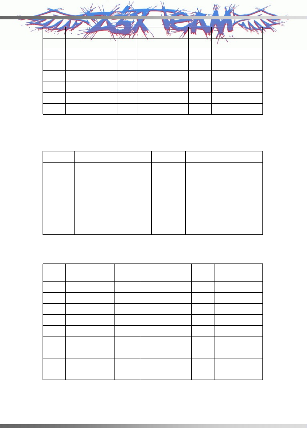
1) Press “##77647269100” + “SEND” and th en, press “000000”
2) Press “1” key for entering “Service Prg.”.
● Usually pressing soft key will sav e the change.
● To exit service program, press “END” key.
3) MEID/ESN
You can see the MEID/ESN number.
Press softkey “OK” to edit more NAM1 items.
Press softkey “Exit” to exit Service Programming.
Z3X-BOX.COM
Copyright © 2007 LG Electronics. Inc. All right reserved
Only for training and service purposes
-16-
LGE Internal Use Only
Page 18
CX9100
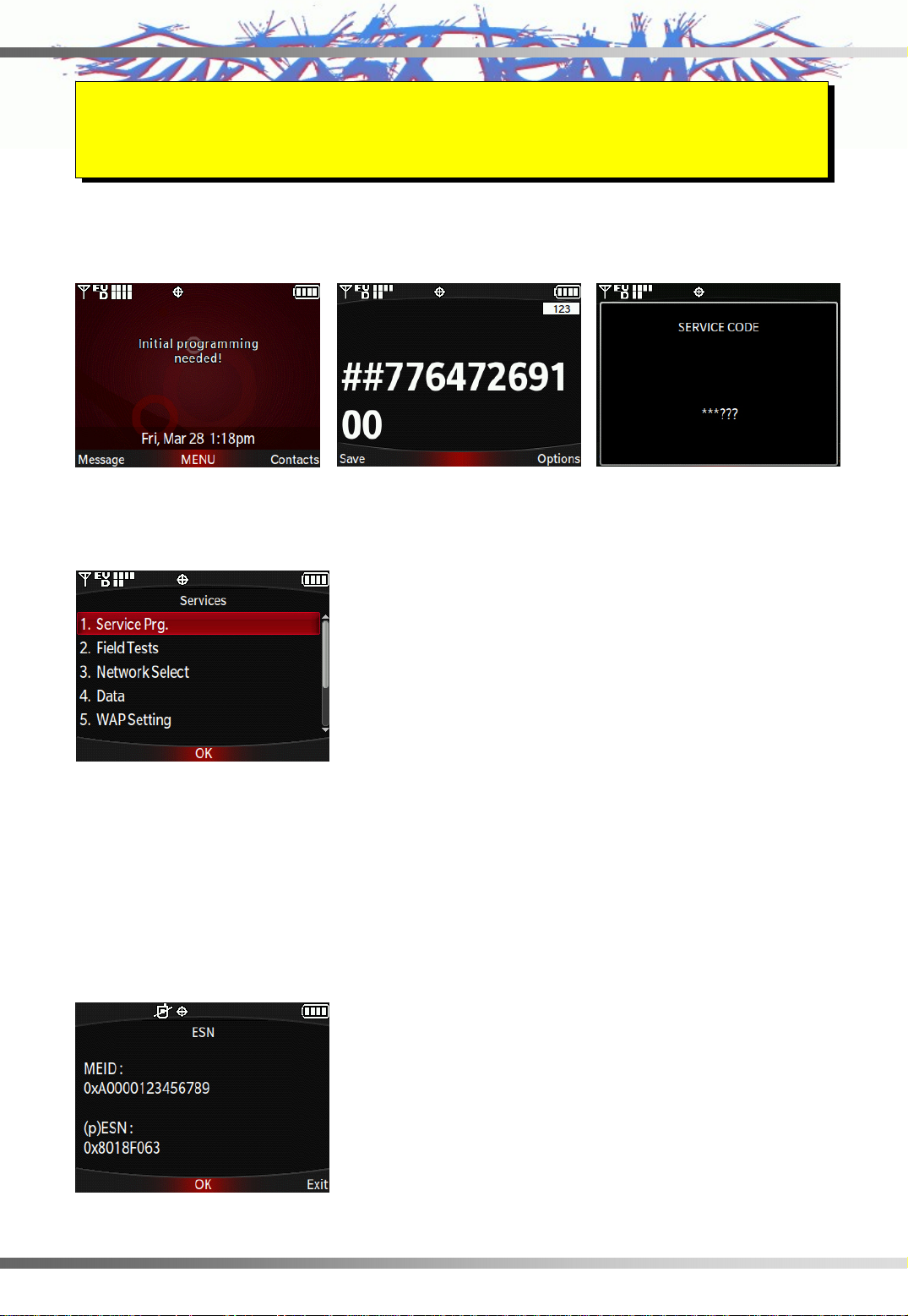
4) NAM1 Phone Number (MDN)
You can edit the NAM1 Phone Number (MDN).
Press softkey “OK” to edit more NAM1 items.
Press softkey “Back” to edit previous NAM1 items.
5) NAM1 Phone Number (MIN)
You can edit the NAM1 Phone Number (MIN).
Press softkey “OK” to edit more NAM1 items.
Press softkey “Back” to edit previous NAM1 items.
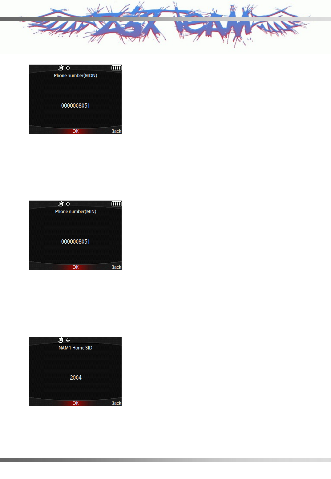
6) NAM1 Home SID
You can edit the NAM1 Home SID.
Press softkey “OK” to edit more NAM1 items.
Press softkey “Back” to edit previous NAM1 items.
Z3X-BOX.COM
Copyright © 2007 LG Electronics. Inc. All right reserved
Only for training and service purposes
-17-
LGE Internal Use Only
Page 19
CX9100
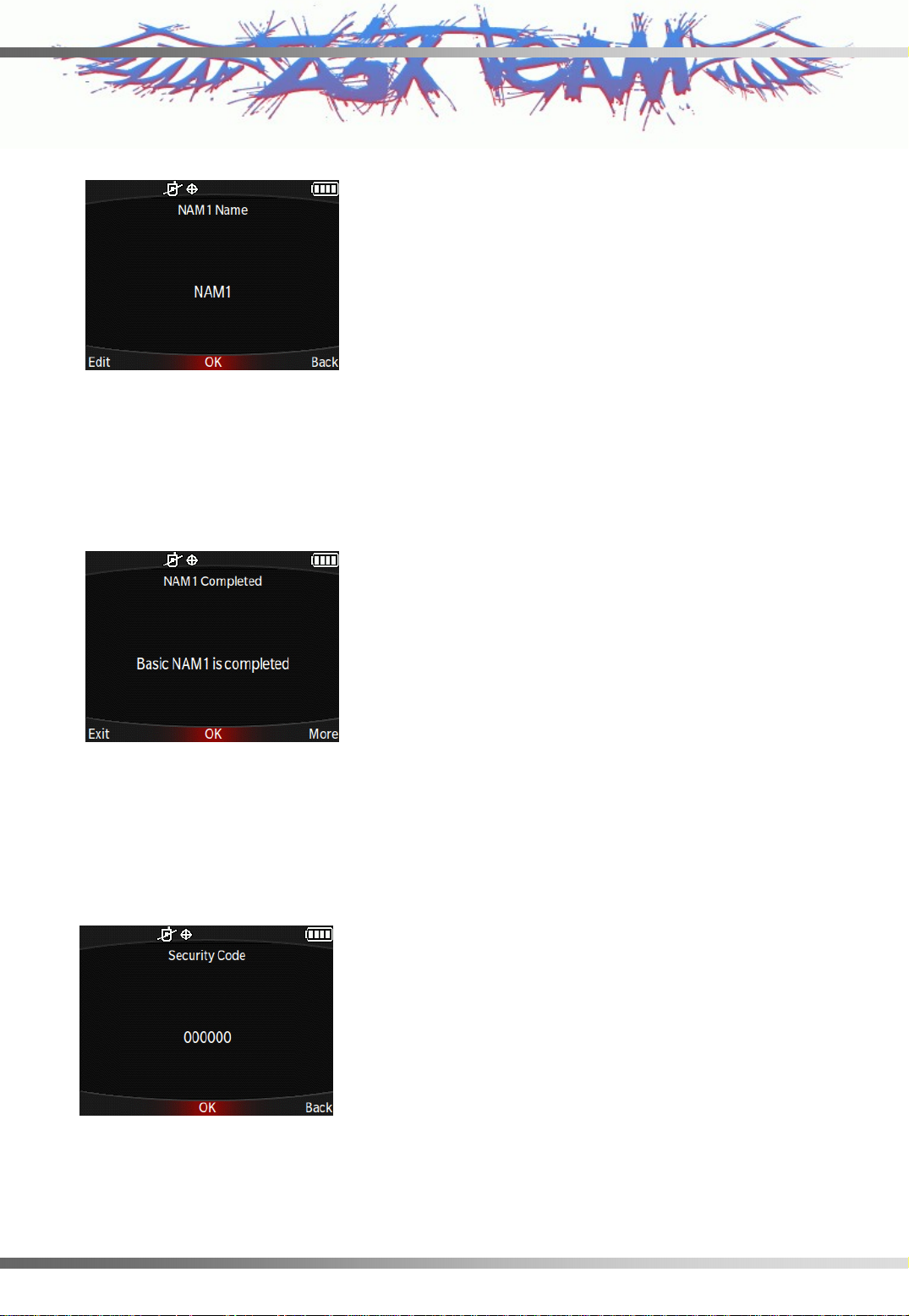
7) NAM1 Name
You can edit the NAM1 Name.
Press softkey “OK” to edit more NAM1 items.
Press softkey “Back” to edit previous NAM1 items.
8) More NAM1 Programming
You can decide to edit more NAM1 Name.
Press softkey “OK” to exit Service Programming.
Press softkey “More” to edit more advanced NAM1 items.
9) Service Code
You can edit Service Code.
Press softkey “OK” to edit more NAM1 items.
Press softkey “Back” to edit previous NAM1 items.
Z3X-BOX.COM
Copyright © 2007 LG Electronics. Inc. All right reserved
Only for training and service purposes
-18-
LGE Internal Use Only
Page 20
CX9100
10) NAM1 MCC
You can edit NAM1 Mobile Country Code.
Press softkey “OK” to edit more NAM1 items.
Press softkey “Back” to edit previous NAM1 items.
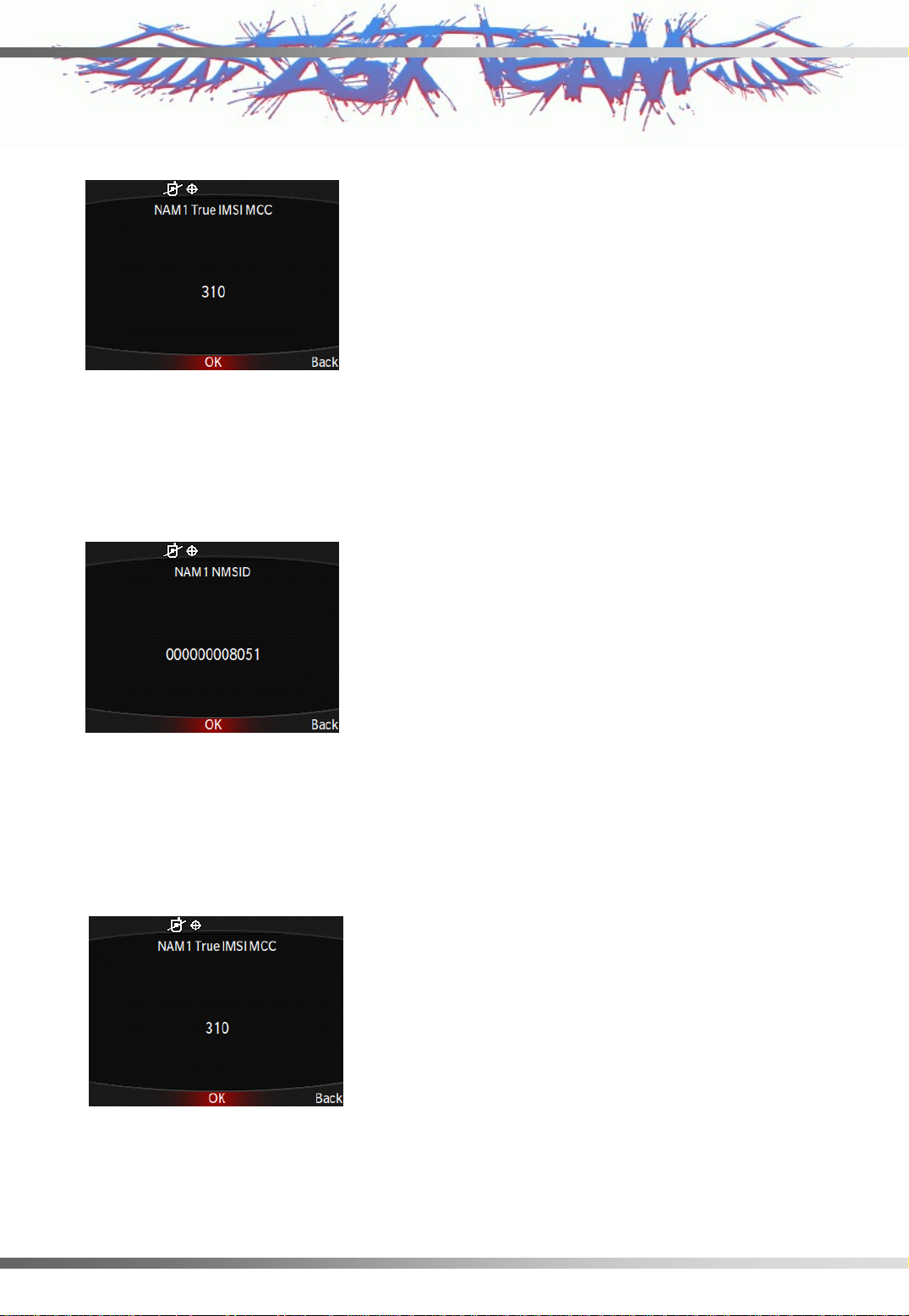
11) NAM1 NMSID
You can edit NAM1 NMSID.
Press softkey “OK” to edit more NAM1 items.
Press softkey “Back” to edit previous NAM1 items.
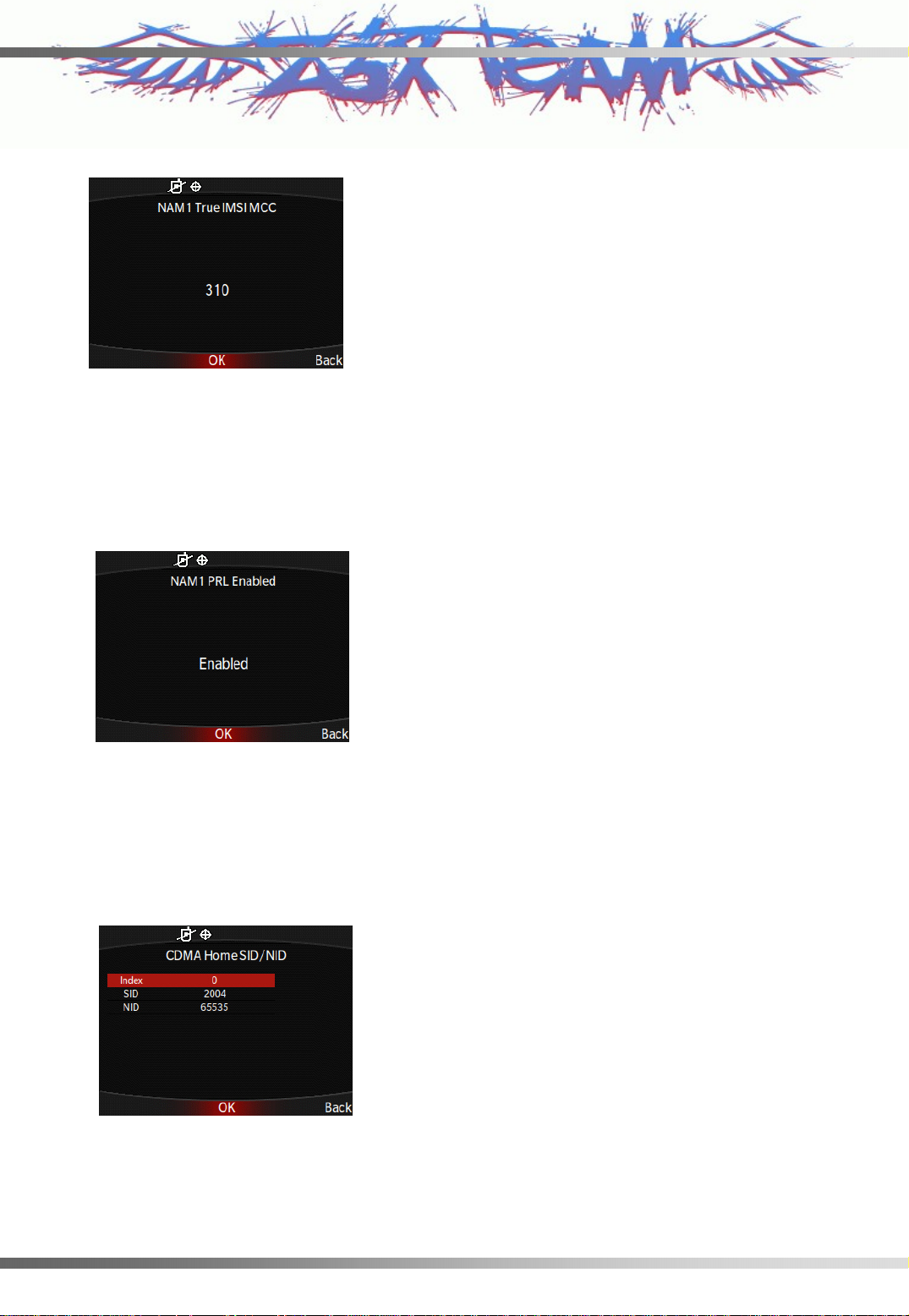
12) NAM1 True IMSI MCC
You can edit NAM1 True IMSI MC
Press softkey “OK” to edit more NAM1 items.
Press softkey “Back” to edit previous NAM1 items.
C.
Z3X-BOX.COM
Copyright © 2007 LG Electronics. Inc. All right reserved
Only for training and service purposes
-19-
LGE Internal Use Only
Page 21
CX9100
13) NAM1 True IMSI NMSID
You can edit NAM1 True IMSI NMSID.
Press softkey “OK” to edit more NAM1 items.
Press softkey “Back” to edit previous NAM1 items.
14) NAM1 PRL Enabled
You can see NAM1 PRL Enabled.
Press softkey “OK” to edit more NAM1 items.
Press softkey “Back” to edit previous NAM1 items.
15) CDMA Home SID/NID
You can edit NAM1 Home SID/NID pair.
Press softkey “OK” to edit more NAM1 items.
Press softkey “Back” to edit previous NAM1 items.
Z3X-BOX.COM
Copyright © 2007 LG Electronics. Inc. All right reserved
Only for training and service purposes
-20-
LGE Internal Use Only
Page 22
CX9100
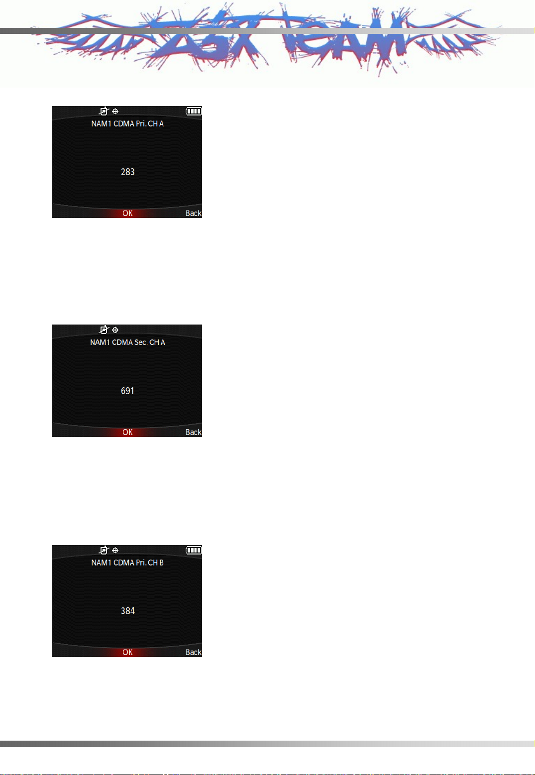
16) NAM1 CDMA Pri. CH A
You can edit NAM1 CDMA Pri. Channel A.
Press softkey “OK” to edit more NAM1 items.
Press softkey “Back” to edit previous NAM1 items.
17) NAM1 CDMA Sec. CH A
You can edit NAM1 CDMA Secondary Channel A.
Press softkey “OK” to edit more NAM1 items.
Press softkey “Back” to edit previous NAM1 items.
18) NAM1 CDMA Pri. CH B
You can edit NAM1 CDMA Primary Channel B.
Press softkey “OK” to edit more NAM1 items.
Press softkey “Back” to edit previous NAM1 items.
Z3X-BOX.COM
Copyright © 2007 LG Electronics. Inc. All right reserved
Only for training and service purposes
-21-
LGE Internal Use Only
Page 23
CX9100
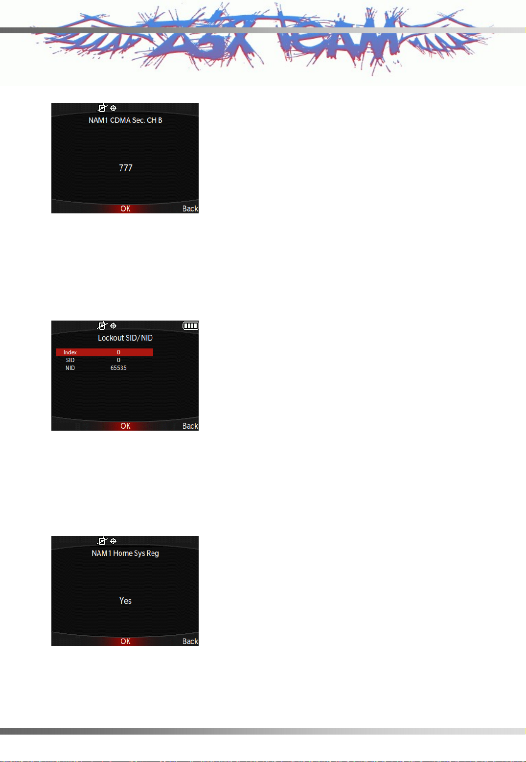
19) NAM1 CDMA Sec. CH B
You can edit NAM1 CDMA Secondary Channel B.
Press softkey “OK” to edit more NAM1 items.
Press softkey “Back” to edit previous NAM1 items.
20) Lockout SID/NID
You can edit Lockout SID/NID pair.
Press softkey “OK” to edit more NAM1 items.
Press softkey “Back” to edit previous NAM1 items.
21) NAM1 Home Sys. Reg.
You can edit NAM1 Home System Registration.
Press softkey “OK” to edit more NAM1 items.
Press softkey “Back” to edit previous NAM1 items.
Z3X-BOX.COM
Copyright © 2007 LG Electronics. Inc. All right reserved
Only for training and service purposes
-22-
LGE Internal Use Only
Page 24
CX9100
22) NAM1 Forn SID Reg
You can edit NAM1 Foreign SID Registration.
Press softkey “OK” to edit more NAM1 items.
Press softkey “Back” to edit previous NAM1 items.
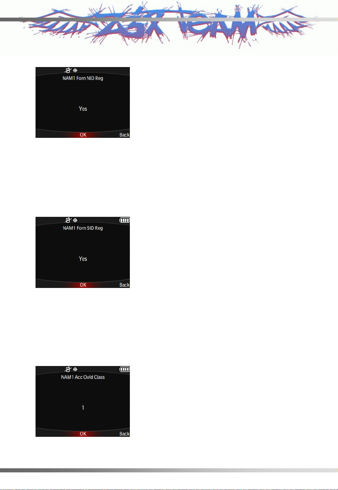
23) NAM1 Forn NID Reg
You can edit NAM1 Foreign NID Registration.
Press softkey “OK” to edit more NAM1 items.
Press softkey “Back” to edit previous NAM1 items.
24) NAM1 ACC Ovld Class
You can view the NAM1 Access Overload Class.
Press softkey “OK” to edit more NAM1 items.
Press softkey “Back” to edit previous NAM1 items.
Z3X-BOX.COM
Copyright © 2007 LG Electronics. Inc. All right reserved
Only for training and service purposes
-23-
LGE Internal Use Only
Page 25
CX9100
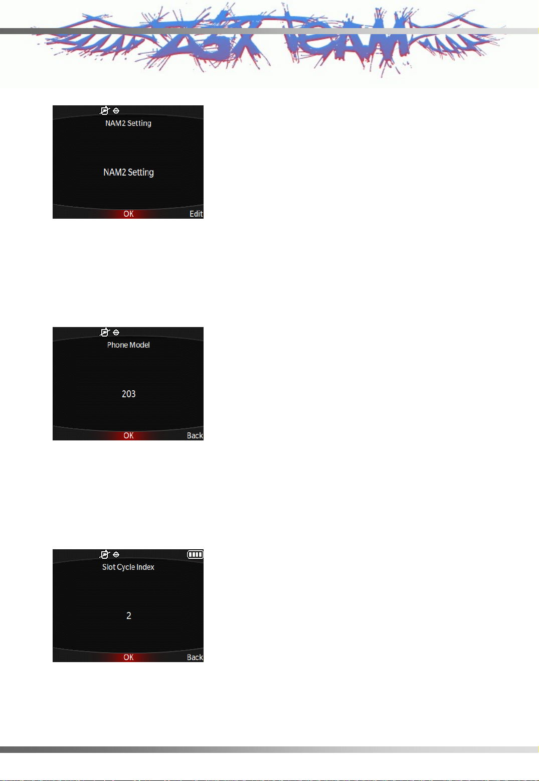
25) NAM2 Setting
You can decide to edit NAM2 items.
Press softkey “OK” to skip NAM2 items setting.
Press softkey “Edit” to edit NAM2 related items. You can edit NAM2 items such as NAM1 items
26) Phone Model
You can see the Phone Model Number.
Press softkey “OK” to edit more items.
Press softkey “Back” to edit previous items.
27) Slot Cycle Index
You can edit Slot Cycle Index.
Press softkey “OK” to save Slot Cycle Index.
Press softkey “Back” to edit previous items.
Z3X-BOX.COM
Copyright © 2007 LG Electronics. Inc. All right reserved
Only for training and service purposes
-24-
LGE Internal Use Only
Page 26

CX9100
28) Powering Down
Restart.
Z3X-BOX.COM
Copyright © 2007 LG Electronics. Inc. All right reserved
Only for training and service purposes
-25-
LGE Internal Use Only
Page 27

CX9100
CHAPTER 3. Circuit Description
CHAPTER 3. Circuit Description
1. RF Transmit/Receive Part
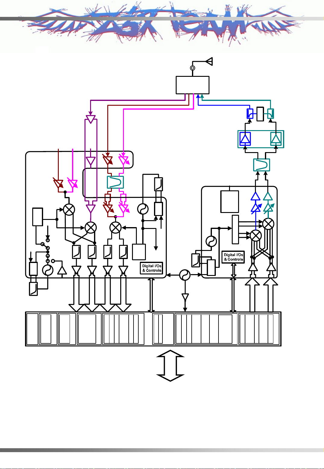
1.1 Overview
The TX and RX part employs the Direct-Conversion system. The TX and RX frequencies are respectively
824.04~848.97 and 869.04~893.97 for cellular and 1850~1910 and 1930~1990 for PCS. The block diagram is shown
in [Figure 1-1]. CDMA RF signals received through the antenna are separated by the Diplexer.
RF Signal fed into the low noise amplifier in RFR6500(LNA) through the duplexer. Then, they are fed into Mixer in
RFR6500. In RFR6500, the RF signal is changed into baseband signal directly. Then, this signal is changed into
digital signal by the analog to digital converter (ADC, A/D Converter), and the digital circuit part of the
MSM(Mobile Station Modem) 6550 processes the data from ADC. The digital processing part is a demodulator.
In the case of transmission, RFT6150 receives OQPSK-modulated analog signal from the MSM6550A.
The RFT6150 connects directly with MSM6550A using an analog baseband interface. In RFT6150, the baseband
quadrature signals are upconverted to the Cellular or PCS frequency bands and amplified to provide signal drive
capability to the power amp.
After that, the RF signal is amplified by the Power Amp in order to have enough power for radiation. Finally, the RF
signal is sent out to the cell site via the antenna after going through the duplexer.
Z3X-BOX.COM
Copyright © 2007 LG Electronics. Inc. All right reserved
Only for training and service purposes
-26-
LGE Internal Use Only
Page 28
CX9100
[Figure 1-1] RF Block Diagram of VX9100
Antenna
CDMA
DCN-Rx
DCN-Tx
PCS-Rx
PCS-Tx
GPS
HDET
RFR6500
F
ref
Loop Filter
for GPS
Processing
&Dist
PLL1
Camera
LO Gen
GPS VCO
3D, 2D
NC
Diversity Rx
VCO
OpenGL® ES
Graphics
Dual PAM
NC
H.263, H.264
MPEG-4
NC
Dual SAW
Rx RF
RFT6150
CDMA VCOs
Secondary Path
Rx1_Q
EVRC, QCELP
AMR, CMX,
Video
MP3, AAC,
MIDI
Rx1_I
Audio
Primary Path
Rx0_Q
UART2/RUIM1
UART3/RUIM2
&Dist
Gen
Rx0_I
USB On The
Keypad I/F
SD/SDIO
UART1
Go
PLL0
Diversity
Rx VCO
LO
SBI Control
MSM6500
Connectivity
EBI2
for CDMA Tx
F
ref
F
ref
Dual Memory
Rx ADC
Buses
EBI1
Loop Filter
VCTCXO
Buffer
Ref.
Bluetooth 1.1
Processor
Processor
Tx DAC
SBI
gpsOne
TX PLL
Processor
Circuits
Control
Tx VCO
Processor 1X,
GSM/GPRS
1X EV-DO
CDMA
Gain
Processors
PCS
DCN
Dual SAW
Tx RF
LO Gen &Dist
SBI Control
Tx_Q
QDSP4000
QDSP4000
Modem
PLL
Tx_I
ARM926EJS
with Jazelle
MSM
JTAG I/F
Z3X-BOX.COM
Copyright © 2007 LG Electronics. Inc. All right reserved
Only for training and service purposes
Logic
Device
-27-
LGE Internal Use Only
Page 29
CX9100
1.2 Description of RX Part Circuit
1.2.1 Quintplexer (DP100)
The Quintplexer consists of the Rx bandpass filter (BPF), the Tx BPF and the GPS filter (BPF) which has the
function of separating Tx, Rx and GPS signals in the full Triplex system for using the common antenna. The Tx part
BPF is used to suppress noises and spurious out of the Tx frequency band. The Rx BPF is used to receive only Rx
signal coming from the antenna, which is usually called preselector. It’s main function is to limit the bandwidth of
spectrum reaching the LNA and mixer, attenuate receiver spurious response and suppress local oscillator energy. As
a result frequency sensitivity and selectivity of mobile phone increas e. The specification of VX9100 Quintplexer
described below;
z PCS band
Tx Rx Tx to Rx (min)
Pass Band 1850.5~1909.5 MHz 1930.5~1989.5 MHz
Insertion Loss 3.9 dB max 4.2 dB max
Return Loss 9.5 dB min 9.0dB min
Attenuation
z Cellular band
Pass Band 824~849 MHz 869~894 MHz
Insertion Loss 2.6 dB max 3.4 dB max
Return Loss 9.0 dB min 9.0dB min
Attenuation
z GPS band
Pass Band 1574.42~1576.42MHz
Insertion Loss 1.9 dB m a x
40 dB min
(1930.5~1989.5MHz)
Tx Rx Tx to Rx (min)
40 dB min
(869~894MHz)
(1850.5~1909.5MHz)
(824~849MHz)
Z3X-BOX.COM
50dB min
55dB min
53 dB (1850.5~1909.5MHz)
40 dB (1930.5~1909.5MHz)
5
5 dB (824~894MHz)
40 dB (869~894MHz)
Return Loss 9 min
Isolation1 50 dB min(Cel
Isolation2 45 dB min(PCS Tx à GPS)
Copyright © 2007 LG Electronics. Inc. All right reserved
Only for training and service purposes
l Tx à GPS)
-28-
LGE Internal Use Only
Page 30
CX9100
1.2.2 RFR6500 – LNA part (U108)
The RFR6500 has cellular, and PCS LNA, respectively. The characteristics of Low Noise Amplifier (LNA) are low
noise figure, high gain, high intercept point and high reverse isolation. The frequency selectivity characteristic of
mobile phone is mostly determined by LNA.
The specification of VX9100 LNA is described below:
Parameter
Gain -19 -20 3 -3 14 15 dB
Noise Figure 20 20 4.5 6 1.3 1.1 dB
Input IP3 10 10 5 10 7 3 dBm
1.2.3 GPS LNA(U101)
The characteristics of Low Noise Amplifier (LNA) are low noise figure, high gain, high intercept point and high
reverse isolation. The frequency selectivity ch aracteristic of mobile phone is mostly determined by LNA.
The specification of VX9100 GPS LNA is described below
Low gain Middle gain High gain Units
Cellular PCS Cellular PCS Cellular PCS
UnitsGPS BandParameter
dB13.1Gain
dB0.77Noise Figure
dBm3.41dB compression point
dBm+7IIP3
1.2.4 RX RF Dual SAW Filter(F100)
The main function of RX RF SAW filter is to attenuate mobile phone spurious frequency, attenuate noise amplified
by the LNA and suppress second harmonic originating in the LNA.
Z3X-BOX.COM
Copyright © 2007 LG Electronics. Inc. All right reserved
Only for training and service purposes
-29-
LGE Internal Use Only
Page 31

CX9100
1.2.5 RFR6500 - Down-converter Mixers part (U108)
The RFR6500 device performs signal down-conversion for Cellular, PCS and GPS tri-band applications. It contains
all the circuitry (with the exception of external filters) needed to support conversion of received RF signals to Baseband signals. The three down-converting Mixers (Cellular, PCS and GPS), and a programmable PLL for generating
RX LO frequency and an RX LO Buffer Amplifier and RX Voltage Controlled Oscillator. The GPS LNA & mixers
offer the most advanced and integrated CDMA RX solution designed to meet cascaded Noise Figure (NF) and Thirdorder Intercept Point (IIP3) requirements of IS-98D and J-STD-018 specifications for Sensitivity, Two-Tone Intermodulation, and Single-tone Desensitization.
Operation modes and band selection are specially controlled from the Mobile Station Modem
MSM6550A.
The specification of VX9100 Mixers is described below:
Parameter
Noise Figure 25 27 7.9 12 dB
Input IP3 -5 -11 4 4 dBm
Input IP2 30 30 56 56 dBm
Low gain High gain Units
Cellular PCS Cellular PCS
1.3 Description of Transmit Part Circuit
1.3.1 RFT6150 (U109)
The RFT6150 Base-band to RF Transmit Processor performs all TX signal-processing functions required between
digital Base-band and the Power Amplifier Modulator (PAM). The Base-band quadrate signals are up-converted to
the Cellular or PCS frequency bands and amplified to provide signal d rive capability to the PAM. The RFT6150
includes mixers for up-converting analog Base-band to RF, a programmable PLL for generating TX LO frequency a
TX LO Buffer Amplifier and TX Voltage Controlled Oscillator, cellular and PCS driver amplifiers and TX power
control through an 85 dB VGA. As added benefit, the single sideband up-conversion eliminates the need for a band
pass filter normally required between the up-converter and driver amplifier.
I, I/, Q and Q/ signals proceed from the MSM6550A to RFT6150 are analog signal. In CDMA mode, These signals
are modulated by Offset Quadrature Phase Shift King (OQPSK). I and Q are 90 deg. out of phase, and I and I/ are
180 deg. The mixers in RFT6150 converts baseband signals into RF signals. After passing through the upconverters,
RF signal is inputted into the Power AMP.
Z3X-BOX.COM
Copyright © 2007 LG Electronics. Inc. All right reserved
Only for training and service purposes
-30-
LGE Internal Use Only
Page 32

CX9100
zRFT6150 Cellular and PCS CDMA R F Specifications
Parameter Condition Min. Type. Max. Units
Rated Output Power
Min Output Power
RX band noise power
ACPR
1.3.2 Dual Power Amplifier(U105)
The Dual power amplifier that can be used in the PCS and CDMA mode has linear amplification capability and high
efficiency. For higher efficiency, it is made up of one MMIC (Monolithic Microwave Integrated Circuit) for which
RF input terminal and internal interface circuit are integrated onto one IC after go ing through the AlGaAs/GaAs HBT
(heterojunction bipolar transistor) process. The module of power amplifier is made up of an output end interface
circuit including this MMIC. The maximum power that can be inputted through the input terminal is +10dBm and
conversion gain is about 26.5dB. RF transmit signals that have been amplified through the power amplifier are sent to
the duplexer.
.
Average CDMA Cellular
Average CDMA PCS
Average CDMA Cellular
Average CDMA PCS
CDMA Cellular
CDMA PCS
Cellular: Fc±885kHz
PCS : Fc±1.25MHz
7
9
-75
-75
-136
-133
-56
-57
dBm
dBm
dBm
dBm
dBm/Hz
dBc/30kHz
1.4 Description of Frequency Synthesizer Circuit
1.4.1 Voltage Control Temperature Compensation Crystal Oscillator (VCTCXO, U107)
The temperature variation of mobile phone can be compensated by VCTCXO. The reference frequency of a mobile
phone is 19.2 MHz. The receiver frequency tuning signals called TRK_LO_ADJ from MSM as 0.5 V~2.5 V DC via
R and C filter in order to generate the reference frequency of 19.2 MHz and input it into the frequency synthesizer.
Frequency stability depending on temperature is ±2.0 ppm.
Z3X-BOX.COM
Copyright © 2007 LG Electronics. Inc. All right reserved
Only for training and service purposes
-31-
LGE Internal Use Only
Page 33

CX9100
2. Digital/Voice Processing Part
2.1 Overview
The digital/voice processing part processes the user's commands and processes all the digital and voice signal
processing in order to operate in the phone. The digital/voice processing part is made up of a main keypad/touch
keypad/LCD, receptacle part, voice processing part, mobile station modem part, memory part, and power supply part.
2.2 Configuration
2.2.1 Keypad/LCD and Receptacle Part
This is used to transmit keypad signals to MSM6550A. It is made up of a keypad backlight part that illuminates the
keypad, LCD part that displays the operation status onto the screen, and a receptacle that receives and sends out voice
and data with external sources.
2.2.2 Voice Processing Part
The voice processing part is made up of an audio codec used to convert MIC signals into digital voice signals and
digital voice signals into analog voice signals, amplifying part for amplifying the voice signals and sending them to
the ear piece, amplifying part that amplifies ringer signals coming out from MSM6550A, and amplifying part that
amplifies signals coming out from MIC and transferring them to the audio processor.
2.2.3 MSM (Mobile Station Modem) 6550A Part
MSM is the core elements of CDMA terminal and carries out the functions of CPU, encoder, interleaver,
deinterleaver, Viterbi decoder, Mod/Demod, and vocoder.
2.2.4 Memory Part
The memory part is made up of a NAND Flash memory and a SDRAM for storing data.
2.2.5 Power Supply Part
Z3X-BOX.COM
The power supply part is made up of circuits for generating various types of power, used for the digital/voice
processing part.
Copyright © 2007 LG Electronics. Inc. All right reserved
Only for training and service purposes
-32-
LGE Internal Use Only
Page 34

CX9100
2.3 Circuit Description
2.3.1 Keypad/LCD and Receptacle Part
Once the keypad is pressed, the key signals are sent out to MSM6550A for processing. In addition, when the key is
pressed, the keypad/LCD lights up through the use of 10 LEDs. The terminal status and operation are d isplayed on
the screen for the user with the characters and icons on the LCD.
2.3.2 Audio Processing Part
MIC signals are amplified through OP AMP, inputted into the audio codec (included in MSM6550A) and converted
into digital signals. Oppositely, digital audio signals are converted into analog signals after going through the audio
codec. These signals are amplified at the audio amplifier and transmitted to the ear-piece. The signals from
MSM6550A activate the ringer by using signals generated in the timer in MSM6550A.
2.3.3 MSM Part
MSM6550A is the core element of CDMA system terminal that includes ARM926EJ-S microprocessor core. It
supports both CDMA and Digital FM, operating in both the cellular and PCS spectrums. The subsystems within the
MSM6550A include a CDMA processor, a DFM processor, a multi-standard Vocoder, an integrated CODEC with
earpiece and microphone amplifiers, general-purpose ADC for subsystem monitoring, an ARM926EJ-S
microprocessor, and Universal Serial Bus (USB) supporting forward and reverse link data communications of 307.2
Kbps simultaneously. And it also contains complete digital modulation and demodulation systems for CDMA
standards, as specified in IS-95-A/B/C. In MSM, coded symbols are interleaved in order to cope with multi-path
fading. Each data channel is scrambled by the long code PN sequence of the user in order to ensure the
confidentiality of calls. Moreover, binary quadrature codes are used based on Walsh functions in order to discern
each channel. Data created thus are 4-phase modulated by one pair of Pilot PN code and they are used to create I and
Q data. When received, I and Q data are demodulated into symbols by the demodulator, and then de-interleaved in
reverse to the case of transmission. Then, the errors of data received from Viterbi decoder are detected and corrected.
They are voice-decoded at the vocoder in order to output digital voice data.
Z3X-BOX.COM
Copyright © 2007 LG Electronics. Inc. All right reserved
Only for training and service purposes
-33-
LGE Internal Use Only
Page 35

CX9100
[Figure 2-2] Block Diagram of Digital/Voice Processing Part
Antenna
CDMA
DCN-Rx
DCN-Tx
PCS-Rx
PCS-Tx
GPS
HDET
for GPS
RFR6500
F
ref
Loop Filter
Processing
&Dist
PLL1
Camera
LO Gen
GPS VCO
VCO
OpenGL® ES
3D, 2D
NC
Diversity Rx
H.263, H.264
Graphics
MPEG-4
Dual PAM
NC
NC
Dual SAW
Rx RF
RFT6150
CDMA VCOs
Secondary Path
Rx1_I
Rx1_Q
EVRC, QCELP
AMR, CMX,
Video
MP3, AAC,
MIDI
Primary Path
Rx0_Q
UART2/RUIM1
UART3/RUIM2
Audio
&Dist
Gen
Rx0_I
USB On The
Keypad I/F
SD/SDIO
UART1
Go
PLL0
Diversity
Rx VCO
LO
Digital I/Os
& Controls
SBI Control
MSM6500
Connectivity
EBI2
F
ref
Buses
EBI1
F
ref
Dual Memory
for CDMA Tx
Loop Filter
VCTCXO
Buffer
Ref.
Bluetooth 1.1
Processor
Rx ADC
SBI
Processor
Tx DAC
Circuits
Control
Gain
Tx VCO
Digital I/Os
& Controls
TX PLL
Processors
Processor 1X,
GSM/GPRS
Processor
1X EV-DO
gpsOne
CDMA
PCS
DCN
Dual SAW
Tx RF
LO Gen &Dist
SBI Control
Tx_I
Tx_Q
ARM926EJS
QDSP4000
Modem
with Jazelle
PLL
JTAG I/F
MSM
QDSP4000
Z3X-BOX.COM
Qwerety Keypad
Qwerty Key
IC
A
Z
S
X
DF
CV
G
B
H
N
Q
W
ER
T
Y
Image Sensor
2.0M CMOS,
(MAX9775)
Stereo Headset
Sub-System
Audio
Receiver
MIC
Speaker
Stereo
Micro SD
Copyright © 2007 LG Electronics. Inc. All right reserved
Only for training and service purposes
Keypad
*
0#
456
123
789
-34-
16bit
EBI1
EBI2
USB 1.1 FS
Bluetooth v1.1
(LP3922)
PMIC
Main (240x320, 260K)
Sub (64x160, 260K)
LCD
Bluetooth v1.1
RF Module
Bluetooth
8bit
MCP
512MBit
SDRAM
NAND
1GBit
(CAM_DVDD/CA
M_AVDD/CAM_I
Sub PMIC
OVDD)
LGE Internal Use Only
Page 36

CX9100
2.3.4 Memory Part
MCP contents 1024Mbits NAND FLASH memory and 512Mbits SD RAM. In the NAND Flash Memory part of
MCP are programs used for terminal operation. The programs can be changed through downloading after the
assembling of terminals. On the SDRAM data generated during the terminal operation are stored temporarily.
2.3.5 Power Supply Part
POWER ON mode will be activated by a POWER_ON_SW signal or the insertion of a charger input voltage
(V_CHAR). During the Power On Sequence the output voltages MSMC(Buck1), MSMP1(Buck2), MSMP2(LOD1),
MSMA(LDO4) and LCD(LDO2) will be activated in a sequence. Reset (RESIN\) will be released in order to power
the host processor up properly. when MSMx[*] reaches 87% of its final value, a 60ms reset timer is started. Now the
BB Processor is initialized and will assert PS_HOLD signal high within 60ms. PS_HOLD maintains the power on.
The two Buck converters / LDO1,2,4 in PMIC are generating the +1.275V_MSMC, +1.85V_MSMP1,
+2.6V_MSMP2, +2.8V_LCD, and +2.6V_MSMA respectively.
The Rx part LDO3 in PMIC is operated by the control signal SLEEP/ from MSM6550A
The Tx part LDO4 in PMIC is operated by the control signal IDLE/ from MSM6550A.
The TCXO part LDO5 in PMIC is operated by the control signal TCXO_EN/ from MSM6550A.
2.3.6 Logic Part
The logic part consists of internal CPU of MSM, RAM, MCP. The MSM6550A receives TCXO (=19.2MHz) from
the U1010 and controls the phone in CDMA modes. The major components are as follows:
CPU
The ARM926EJ-S microprocessor includes a 3 stage p ipelined RISC architecture, both 32-bit ARM and 16-bit
THUMB instruction sets, a 32-bit address bus, and a 32-bit internal data bus. It has a high performance and low
power consumption.
MCP
NAND Flash is used to store the terminal’s program. Using the down-loading program, the program can be
changed even after the terminal is fully assembled.
SDRAM is used to store the internal flag information, call processing data, and timer data.
KEYPAD
For key recognition, key matrix is setup using key encoder IC . 5 LEDs and backlight circuitry are includ e d in the
keypad for easy operation in the dark.
LCD MODULE
LCD module contains a controller which will display the information onto the LCD by 16-bit data from the
MSM6550A. It is also supplied stable +2.8V_LCD by Out6 in U5002 for wide view angle and LCD reflects to
improve the display efficiency. 7 LEDs is used to display LCD backlight.
Z3X-BOX.COM
Copyright © 2007 LG Electronics. Inc. All right reserved
Only for training and service purposes
-35-
LGE Internal Use Only
Page 37

CX9100
4.1 Rx Part Trouble
4.1.1 DCN Rx
CHAPTER 4. Trouble Shooting
CHAPTER 4. Trouble Shooting
Test Point
Test Point
Mobile S/W
Quintplexer
Start
Rx TEST SETUP (Joyphone)
- Tes t C hann el: 3 8 4
- Test Band : US Cellular
- SID: 2004
- Sector Power: - 30 dB m Spec trum Analyzer Setting
Oscilloscope Setting
1. Check
DC Power Supply circuit
Z3X-BOX.COM
RFR6500
VCTCXO
Check flow
Check flow
3. Check
Control signal
4. Check
RF Signal path
2. Check
VCTCXO
Copyright © 2007 LG Electronics. Inc. All right reserved
Only for training and service purposes
-36-C
NO
5. Check
Rx I/Q data
Redownload S /W , Cal
LGE Internal Use Only
Page 38

CCX9100
4.1.1.1 Checking DC Power supply circuit (PMIC)
Test Point
Test Point
R431
C432
Circuit Diagram
Circuit Diagram
TP1
TP2
Z3X-BOX.COM
Copyright © 2007 LG Electronics. Inc. All right reserved
Only for training and service purposes
-37-CC
LGE Internal Use Only
Page 39

CX9100
Start
Checking Flow
Checking Flow
Check C432(TP2)
+
2
85 V_ RX is OK?
.
YES
Check R431(TP1)
+2.6V_MSMP2 is OK?
YES
DC Po wer supply Circuit is OK. See next Page to check
VCTCXO circuit
NO
NO
The Problem may be Logic part
Refer to Logic troubleshoot
The Problem may be Logic part
Refer to Logic troubleshoot
Z3X-BOX.COM
Copyright © 2007 LG Electronics. Inc. All right reserved
Only for training and service purposes
-38-
LGE Internal Use Only
Page 40

CX9100
4.1.1.2 Checking VCTCXO circuit
R111
pin4
U107
pin3
Test Point
Test Point
C181
TP2
Circuit Diagram
Circuit Diagram
Z3X-BOX.COM
TP1
Copyright © 2007 LG Electronics. Inc. All right reserved
Only for training and service purposes
-39-
LGE Internal Use Only
Page 41

CX9100
Start
Checking Flow
Checking Flow
Check U107 pin3(TP1)
Is it 19.2MHz? (Refer to
figure 4.1.1 (a))
NO
Check U107 pin4(TP2)
Is it 2.85 V? (Refer to
figure 4.1.1 (b))
YES
Replace U107 and then check R111 , C181 .
Is it similar?
NO
Replace Main B /D
VCTCXO circuit is Ok . See next page
YES
NO
YES
to check control signal .
The Problem may be Logic part
Referto Logic troubleshoot
VCTCXO circuit is Ok . See next page
to check control signal .
Z3X-BOX.COM
Figure 4.1.1 (a) Figure 4.1.1 (b)
Copyright © 2007 LG Electronics. Inc. All right reserved
Only for training and service purposes
Waveform
Waveform
-40-
LGE Internal Use Only
Page 42

CX9100
4.1.1.3 Checking Control signal
U108 pin49(SBST0)
pin50(SBDT0)
pin51(SBCK0)
Test Point
Test Point
Circuit Diagram
Circuit Diagram
Z3X-BOX.COM
Copyright © 2007 LG Electronics. Inc. All right reserved
Only for training and service purposes
-41-
LGE Internal Use Only
Page 43

CX9100
Start
Checking Flow
Checking Flow
Check if there is any major difference referring
Check if there is any major difference referring
Check pin49, 50, 51 at U108
To Figure 4.1.1 (c), (d)
NO
Redownload S/W
Check pin49, 50, 51 at U108
To Figure 4.1.1 (c), (d)
NO
Replace Main B /D
Waveform
Waveform
YES
YES
Control signal is Ok . See next page
to check RF signal path .
Control signal is Ok . See next page
to check RF signal path .
Z3X-BOX.COM
Figure 4.1.1 (c)
Copyright © 2007 LG Electronics. Inc. All right reserved
Only for training and service purposes
-42-
Figure 4.1.1 (d)
LGE Internal Use Only
Page 44

CX9100
4.1.1.4 Checking RF signal path (Mobile S/W, Quintplexer)
Test Point
Test Point
U100 Pin4
L101,C101,L132
DP100 PIN3
L114,C126,L118,C127
Circuit Diagram
Circuit Diagram
TP1
Z3X-BOX.COM
Copyright © 2007 LG Electronics. Inc. All right reserved
Only for training and service purposes
-43-
TP2
LGE Internal Use Only
Page 45

CX9100
Start
Checking Flow
Checking Flow
Check if there is any major difference referring
To Figure 4.1.1 (e). Is any signal detected at
Check if there is any major difference referring
To Figure 4.1.1 (f ). Is any signal detected at
Check pin2(TP1) at U100
that point?
YES
YES
Is any signal detected at
that point?
YES
Check pin3(TP2) at DP100
that point?
YES
Is any signal detected at
that point?
Z3X-BOX.COM
NO
Replace U100
Check L101,C101,L132
NO
Replace DP100
NO
Check L114,C126,L118,C127
NO
YES
RF signal path is OK. See next page to Rx I/Q data signal
Copyright © 2007 LG Electronics. Inc. All right reserved
Only for training and service purposes
-44-
LGE Internal Use Only
Page 46

CX9100
U100 pin2
Waveform
Waveform
DP100 pin3
4.1.1 (e)
Z3X-BOX.COM
4.1.1 (f)
Copyright © 2007 LG Electronics. Inc. All right reserved
Only for training and service purposes
-45-
LGE Internal Use Only
Page 47

CX9100
4.1.1.5 Checking Rx I/Q data
Test Point
Test Point
U108
Pin7 (RX0_Q_M)
Pin8 (RX0_Q_P)
Pin9 (RX0_I_M)
Pin10 (RX0_I_P)
Circuit Diagram
Circuit Diagram
Z3X-BOX.COM
Copyright © 2007 LG Electronics. Inc. All right reserved
Only for training and service purposes
-46-
LGE Internal Use Only
Page 48

CX9100
Start
Checking Flow
Checking Flow
Check if there is any major difference referring
Redownload S/W, and then recalibrate the Main B/D
Check if there is any major difference referring
All DCN Rx check is completed . If the phone still do
Check pin7, 8, 9, 10 at U108
To Figure 4.1.1 (h), (i)
NO
Check pin7, 8, 9, 10 at U108
To Figure 4.1.1 (h), (i)
NO
not work , change Main B /D .
Waveform
Waveform
YES
Replace U 108
Replace Main B /D
YES
Pin 7 & 8 (RX0_Q_M & RX0_Q_P) Pin 9 & 10 (RX0_I_M & RX0_I_P)
Z3X-BOX.COM
RX0_Q_P
RX0_Q_M
RX_Q_N
Graph 4.1.1(h)
Copyright © 2007 LG Electronics. Inc. All right reserved
Only for training and service purposes
-47-
RX0_I_P
RX0_I_M
RX_Q_N
Graph 4.1.1(i)
LGE Internal Use Only
Page 49

CX9100
4.1.2 PCS Rx
Test Point
Mobile S/W
Quintplexer
RFR6500
Test Point
VCTCXO
Start
Rx TESTSETUP(Joyphone )
- Test C hannel: 675
-TestBand:USPCS
- SID: 4182
- Sect or P ower: - 30 dB m Spec trum Analyzer Setting
Oscilloscope Setting
Z3X-BOX.COM
1. Check
DC Power Supply circuit
2. Check
VCTCXO
Checking Flow
Checking Flow
3. Check
Control signal
4. Check
RF Signal path
NO
5. Check
Rx I/Q data
Copyright © 2007 LG Electronics. Inc. All right reserved
Only for training and service purposes
-48-
Redownload S/W, Cal
LGE Internal Use Only
Page 50

CX9100
4.1.2.1 Checking DC Power supply circuit (PMIC)
Test Point
Test Point
R431
C432
Circuit Diagram
Circuit Diagram
TP1
TP2
Z3X-BOX.COM
Copyright © 2007 LG Electronics. Inc. All right reserved
Only for training and service purposes
-49-
LGE Internal Use Only
Page 51

CX9100
Start
Checking Flow
Checking Flow
Check C432(TP2)
+
2
85 V_ RX is OK?
.
YES
Check R431(TP1)
+2.6V_MSMP2 is OK?
YES
DC Po wer supply Circuit is OK. See next Page to check
VCTCXO circuit
NO
NO
The Problem may be Logic part
Refer to Logic troubleshoot
The Problem may be Logic part
Refer to Logic troubleshoot
Z3X-BOX.COM
Copyright © 2007 LG Electronics. Inc. All right reserved
Only for training and service purposes
-50-
LGE Internal Use Only
Page 52

CX9100
4.1.2.2 Checking VCTCXO circuit
R111
pin4
U107
pin3
Test Point
Test Point
C181
TP2
Circuit Diagram
Circuit Diagram
Z3X-BOX.COM
TP1
Copyright © 2007 LG Electronics. Inc. All right reserved
Only for training and service purposes
-51-
LGE Internal Use Only
Page 53

CX9100
Start
Checking Flow
Checking Flow
Check U107 pin3(TP1)
Is it 19.2MHz? (Refer to
figure 4.1.2 (a))
NO
Check U107 pin4(TP2)
Is it 2.85 V? (Refer to
figure 4.1.2 (b))
YES
Replace U107 and then check R111 , C181 .
Is it similar?
NO
Replace Main B /D
VCTCXO circuit is Ok . See next page
YES
NO
YES
to check control signal .
The Problem may be Logic part
Referto Logic troubleshoot
VCTCXO circuit is Ok . See next page
to check control signal .
Z3X-BOX.COM
Figure 4.1.2 (a) Figure 4.1.2 (b)
Copyright © 2007 LG Electronics. Inc. All right reserved
Only for training and service purposes
Waveform
Waveform
-52-
LGE Internal Use Only
Page 54

CX9100
4.1.2.3 Checking Control signal
U108 pin49(SBST0)
pin50(SBDT0)
pin51(SBCK0)
Test Point
Test Point
Circuit Diagram
Circuit Diagram
Z3X-BOX.COM
Copyright © 2007 LG Electronics. Inc. All right reserved
Only for training and service purposes
-53-
LGE Internal Use Only
Page 55

CX9100
Start
Checking Flow
Checking Flow
Check if there is any major difference referring
Check if there is any major difference referring
Check pin49, 50, 51 at U108
To Figure 4.1.2 (c), (d)
NO
Redownload S/W
Check pin49, 50, 51 at U108
To Figure 4.1.2 (c), (d)
NO
Replace Main B /D
Waveform
Waveform
YES
YES
Control signal is Ok . See next page
to check RF signal path .
Control signal is Ok . See next page
to check RF signal path .
Z3X-BOX.COM
Figure 4.1.2 (c)
Copyright © 2007 LG Electronics. Inc. All right reserved
Only for training and service purposes
-54-
Figure 4.1.2 (d)
LGE Internal Use Only
Page 56

CX9100
4.1.2.4 Checking RF signal path (Mobile S/W, Quintplexer)
Test Point
Test Point
U100 Pin4
L101,C101,L132
DP100 PIN4
L107,C120,L115,C121
Circuit Diagram
Circuit Diagram
TP1
Z3X-BOX.COM
Copyright © 2007 LG Electronics. Inc. All right reserved
Only for training and service purposes
TP2
-55-
LGE Internal Use Only
Page 57

CX9100
Start
Checking Flow
Checking Flow
Check if there is any major difference referring
To Figure 4.1.2 (e). Is any signal detected at
Check if there is any major difference referring
To Figure 4.1.2 (f ). Is any signal detected at
Check pin2(TP1) at U100
that point?
YES
YES
Is any signal detected at
that point?
YES
Check pin4(TP2) at DP100
that point?
YES
Is any signal detected at
that point?
Z3X-BOX.COM
YES
NO
Replace U100
Check L101,C101,L132
NO
Replace DP100
NO
Check L107,C120,L115,C121
NO
RF signal path is OK. See next page to Rx I/Q data signal
Copyright © 2007 LG Electronics. Inc. All right reserved
Only for training and service purposes
-56-
LGE Internal Use Only
Page 58

CX9100
U100 pin2
Waveform
Waveform
DP100 pin4
4.1.2 (e)
Z3X-BOX.COM
4.1.2 (f)
Copyright © 2007 LG Electronics. Inc. All right reserved
Only for training and service purposes
-57-
LGE Internal Use Only
Page 59

CX9100
4.1.2.5 Checking Rx I/Q data
Test Point
Test Point
U108
Pin7 (RX0_Q_M)
Pin8 (RX0_Q_P)
Pin9 (RX0_I_M)
Pin10 (RX0_I_P)
Circuit Diagram
Circuit Diagram
Z3X-BOX.COM
Copyright © 2007 LG Electronics. Inc. All right reserved
Only for training and service purposes
-58-
LGE Internal Use Only
Page 60

CX9100
Start
Checking Flow
Checking Flow
Check if there is any major difference referring
Redownload S/W, and then recalibrate the Main B/D
Check if there is any major difference referring
All DCN Rx check is completed . If the phone still do
Check pin7, 8, 9, 10 at U108
To Figure 4.1.2 (h), (i)
NO
Check pin7, 8, 9, 10 at U108
To Figure 4.1.2 (h), (i)
NO
not work , change Main B /D .
Waveform
Waveform
YES
Replace U 108
Replace Main B /D
YES
Pin 7 & 8 (RX0_Q_M & RX0_Q_P) Pin 9 & 10 (RX0_I_M & RX0_I_P)
Z3X-BOX.COM
RX0_Q_P
RX0_Q_M
RX_Q_N
Graph 4.1.1(h)
Copyright © 2007 LG Electronics. Inc. All right reserved
Only for training and service purposes
-59-
RX0_I_P
RX0_I_M
RX_Q_N
Graph 4.1.1(i)
LGE Internal Use Only
Page 61

CX9100
4.2 Tx Part Trouble Shooting
4.2.1 DCN Tx
Mobile S/W
Test Point
Test Point
DUAL PAM
Tx DUAL
SAW Filter
RFT6150
Checking Flow
Start
Press “##5473784236368” + “SEND” key + “000000” in
Phone idle state.
Press “6” to enter FCC Test
Press “2” to enter CDMA FCC mode
- Set channel to 384 and AGC to 360
Measure frequency domain waveform with Spectrum
analyser
Measure time domain waveform with Oscilloscope
Z3X-BOX.COM
Quintplexer
VCTCXO
Checking Flow
4. Check
RF Dual SAW
5. Check
RF Dual PAM
6. Check
Quintplexer
1. Check
DC Power Supply circuit
2. Check
VCTCXO
3. Check
RFT6150
Copyright © 2007 LG Electronics. Inc. All right reserved
Only for training and service purposes
-60-
NO
7. Check
Mobile Switch
Redownload S/W, Cal
LGE Internal Use Only
Page 62

CX9100
4.2.1.1 Checking DC Power supply circuit (PMIC)
Test Point
Test Point
R431
C435
Circuit Diagram
Circuit Diagram
TP1
Z3X-BOX.COM
TP2
Copyright © 2007 LG Electronics. Inc. All right reserved
Only for training and service purposes
-61-
LGE Internal Use Only
Page 63

CX9100
Start
Checking Flow
Checking Flow
Check C435(TP2)
+
2
85 V_ TX is OK?
.
YES
Check R431(TP1)
+2.6V_MSMP2 is OK?
YES
DC Po wer supply Circuit is OK. See next Page to check
VCTCXO circuit
NO
NO
The Problem may be Logic part
Refer to Logic troubleshoot
The Problem may be Logic part
Refer to Logic troubleshoot
Z3X-BOX.COM
Copyright © 2007 LG Electronics. Inc. All right reserved
Only for training and service purposes
-62-
LGE Internal Use Only
Page 64

CX9100
4.2.1.2 Checking VCTCXO circuit
R111
pin4
U107
pin3
Test Point
Test Point
C181
TP2
Circuit Diagram
Circuit Diagram
Z3X-BOX.COM
TP1
Copyright © 2007 LG Electronics. Inc. All right reserved
Only for training and service purposes
-63-
LGE Internal Use Only
Page 65

CX9100
Start
Checking Flow
Checking Flow
Check U107 pin3(TP1)
Is it 19.2MHz? (Refer to
figure 4.2.1 (a))
NO
Check U107 pin4(TP2)
Is it 2.85 V? (Refer to
figure 4.2.1 (b))
YES
Replace U107 and then check R111 , C181 .
Is it similar?
NO
Replace Main B /D
VCTCXO circuit is Ok . See next page
YES
NO
YES
to check control signal .
The Problem may be Logic part
Referto Logic troubleshoot
VCTCXO circuit is Ok . See next page
to check control signal .
Z3X-BOX.COM
Figure 4.2.1 (a) Figure 4.2.1 (b)
Copyright © 2007 LG Electronics. Inc. All right reserved
Only for training and service purposes
Waveform
Waveform
-64-
LGE Internal Use Only
Page 66

CX9100
4.2.1.3 Checking RFT6150 circuit
TX_Q_P
TX_Q_M
TX_I_P
TX_I_M
Test Point
Test Point
PIN23
PIN 27
PIN 28
PIN 29
PIN 30
PIN 1, 2, 3, 4
PIN15
U109
CELL_OUT
TCXO
TX_ON, SBCK0, SBDT0, SBST0
Circuit Diagram
Circuit Diagram
TP1
Z3X-BOX.COM
TP3
TP4
TP2
Copyright © 2007 LG Electronics. Inc. All right reserved
Only for training and service purposes
-65-
TP5
LGE Internal Use Only
Page 67

CX9100
Start
Checking Flow
Checking Flow
Check if there is any major difference referring
Check pin23(TP1) at U109
To Figure 4.2.1 (c ). Is it similar?
YES
Check I/Q data(TP2) at U109
Check if there is any major difference referring
To Figure 4.2.1 (d ). Is it similar?
YES
Check pin1(TP3) at U109(TX_ON )
whether it is higher than 2.5V.
YES
Check pin15(TP4) at U109(TCXO )
referring to Figure 4.2.1(e). Is it similar?
YES
RFT6150 circuit is OK. See next page
Check U 202 MSM6550
NO
Check TX_ON signal & MSM
NO
Check TCXO circuit.
NO
YES
Check pin2, 3, 4(TP5) at U109
Referring to Figure 4.2.1(f) Is it similar?
YES
Z3X-BOX.COM
Replace U109
NO
Check SBI signal line & MSM
Copyright © 2007 LG Electronics. Inc. All right reserved
Only for training and service purposes
-66-
LGE Internal Use Only
Page 68

CX9100
Waveform
Waveform
Graph 4.2.1(c) Graph 4.2.1 (e)
RX0_Q_P
RX0_Q_M
SBDT
SBCK
RX0_I_P
RX0_I_M
Graph 4.2.1(d)
Z3X-BOX.COM
SBST
SBCK
Graph 4.2.1 (f)
Copyright © 2007 LG Electronics. Inc. All right reserved
Only for training and service purposes
-67-
LGE Internal Use Only
Page 69

CX9100
4.2.1.4 Check RF Tx Dual SAW (DCN)
Test Point
Test Point
U105
(Dual PAM)
D_OUT
F101
D_IN
U109
(RFT6150)
Checking Flow
Checking Flow
Circuit Diagram
Circuit Diagram
TP2
Waveform
Waveform
TP1
Start
Check pin1(TP1)
at F101 . Referring to
Figure 4 .2 .1(g)
Is it similar ?
Check pin9(TP2)
at F101 . Referring to
Figure 4 .2 .1(h)
Is it similar ?
NO
Replace F 101
D_IN fed up with CW signal
D_IN
Check
U109(RFT6150)
YES
Z3X-BOX.COM
RF Tx Dual SAW is
OK
YES
Figure 4.2.1(g)
D_OUT
Copyright © 2007 LG Electronics. Inc. All right reserved
Only for training and service purposes
-68-
Figure 4.2.1(h)
LGE Internal Use Only
Page 70

CX9100
4.2.1.5 Check Dual PAM (DCN) circuit
Test Point
Test Point
RFOUT_CELL
VEN_CEL
L
VCCA
(Dual PAM)
RFIN_CELL
U105
VMODE
VBAT
T
Circuit Diagram
Circuit Diagram
PCS Tx
DCN Tx
TP1
TP4
Z3X-BOX.COM
TP2
TP3
Copyright © 2007 LG Electronics. Inc. All right reserved
Only for training and service purposes
-69-
LGE Internal Use Only
Page 71

CX9100
Start
Checking Flow
Checking Flow
Check pin 2 ,13 (TP1,2) at U105
Check if there is any major difference referring
To Figure 4.2.1(i) Is it similar?
YES
Check pin 4 , 11
whether it is higher than 3.4V.
Check pin3(TP4) at U105(PA_R1 signal)
whether it is lower than 2.2V.
(TP3) at U105(Vcc)
YES
YES
Replace U105
YES
PAM circuit is OK. See next page
Check Vcc line
NO
Check PA_R1 line
NO
Waveform
RFIN_CELL fed up with CW signal
in low gain mode of PAM
Copyright © 2007 LG Electronics. Inc. All right reserved
Only for training and service purposes
Z3X-BOX.COM
Figure 4.2.1(i)
Waveform
RF_IN
-70-
RFOUT_CELL
LGE Internal Use Only
Page 72

CX9100
4.2.1.6 Check Quintplexer (DCN)
Test Point
U103
C115
CELL_TX_PORT
Test Point
ANT_PORT
L132
kwXWW
OxP
TP2
TP3
Circuit Diagram
Circuit Diagram
R127
R126
0
0
L100
6.8n
R129
C102
0
1.5p
R128
C160
0
DNI
1
IN(ANT)
34
U100
RF-800
2
OUT(DUP)
L101
Z3X-BOX.COM
47n
C101
100p
L132
1.8n
TP2
+/-1%
CP0402A0836BNTR
1
4
R103
49.9
CP0402A1880ENTR
3
2
U103
IN
COUPLING
TP1
U102
50OHM
OUT
OUT
50OHM
COUPLING
1608
10u
2
3
4
IN
1
78
L109
C123
1n
20p
C115
3p
C116
1.5p
L133
5.6n
C124
C114
5p
2.2n
L113
DNI
DCN T
PCS T
TP2
DP100
ACFM-7102
6
ANT
CELL_TX
CELL_RX
G_SLUG
7
PCS_TX
PCS_RX
1
2
3
4
5
GPS
L104
5.6n
C105
DNI
TP3
DCN Rx
PCS Rx
GPS
L114
L107
1n
L110
DNI
5.6n
C120
56p
C121
3.3n
L116
DNI
L115
27n
Copyright © 2007 LG Electronics. Inc. All right reserved
Only for training and service purposes
-71-
LGE Internal Use Only
Page 73

CX9100
4.2.1.6 Check Quintplexer (DCN)
Checking Flow
Checking Flow
Start
Check TP1 , TP2
at DP 100 . Referring to
Figure 4.2.1(j)
Is it similar ?
NO
Check TP2 , TP3
at DP 100 . Referring to
Figure 4.2.1(j)
Is it similar ?
NO
Check TP1 , TP3
at DP 100 . Referring to
Figure 4.2.1(j)
Is it similar ?
NO
Replace DP
100 , U103
Quintplexer,
Coupler are OK
YES
Replace U103
(coupler)
YES
Replace DP100
(Quintplexer)
YES
Waveform
Waveform
Z3X-BOX.COM
Tx Port
Figure 4.2.1(j)
Copyright © 2007 LG Electronics. Inc. All right reserved
Only for training and service purposes
-72-
ANT Port
LGE Internal Use Only
Page 74

CX9100
4.2.1.7 Check Mobile S/W
Test Point
Test Point
RF IN
RF OUT
Checking Flow
Checking Flow
Circuit Diagram
Circuit Diagram
TP2
TP1
Waveform
Waveform
Start
Check pin2(TP1) , 1(TP2)
at U100 . Referring to
Figure 4.2.1(k)
Is it similar ?
NO
Replace U100
RF_IN(ANT)
Mobile S/W is
OK
YES
Z3X-BOX.COM
RF_OUT(DUP)
Figure 4.2.1(k)
Copyright © 2007 LG Electronics. Inc. All right reserved
Only for training and service purposes
-73-
LGE Internal Use Only
Page 75

CX9100
4.2.2 PCS Tx
Mobile S/W
Test Point
Test Point
DUAL PAM
Tx DUAL
SAW Filter
RFT6150
Circuit Diagram
Start
Press “##5473784236368” + “SEND” key + “000000” in
Phone idle state.
Press “6” to enter FCC Test
Press “2” to enter PCS FCC mode
- Set channel to 600 and AGC to 360
Measure frequency domain waveform with Spectrum
analyser
Measure time domain waveform with Oscilloscope
Z3X-BOX.COM
Quintplexer
VCTCXO
Circuit Diagram
4. Check
RF Dual SAW
5. Check
RF Dual PAM
6. Check
Quintplexerr
1. Check
DC Power Supply circuit
2. Check
VCTCXO
3. Check
RFT6150
Copyright © 2007 LG Electronics. Inc. All right reserved
Only for training and service purposes
-74-
NO
8. Check
Mobile Switch
Redownload S/W, Cal
LGE Internal Use Only
Page 76

CX9100
4.2.2.1 Checking DC Power supply circuit (PMIC)
Test Point
Test Point
Test Point
Test Point
R431
C435
Circuit Diagram
Circuit Diagram
Z3X-BOX.COM
Copyright © 2007 LG Electronics. Inc. All right reserved
Only for training and service purposes
-75-
TP1
TP2
LGE Internal Use Only
Page 77

CX9100
Start
Checking Flow
Checking Flow
Check C435(TP2)
+
2
85 V_ TX is OK?
.
YES
Check R431(TP1)
+2.6V_MSMP2 is OK?
YES
DC Po wer supply Circuit is OK. See next Page to check
VCTCXO circuit
NO
NO
The Problem may be Logic part
Refer to Logic troubleshoot
The Problem may be Logic part
Refer to Logic troubleshoot
Z3X-BOX.COM
Copyright © 2007 LG Electronics. Inc. All right reserved
Only for training and service purposes
-76-
LGE Internal Use Only
Page 78

CX9100
4.2.2.2 Checking VCTCXO circuit
R111
pin4
U107
pin3
Test Point
Test Point
C181
TP2
Circuit Diagram
Circuit Diagram
Z3X-BOX.COM
TP1
Copyright © 2007 LG Electronics. Inc. All right reserved
Only for training and service purposes
-77-
LGE Internal Use Only
Page 79

CX9100
Start
Checking Flow
Checking Flow
Check U107 pin3(TP1)
Is it 19.2MHz? (Refer to
figure 4.2.2 (a))
NO
Check U107 pin4(TP2)
Is it 2.85 V? (Refer to
figure 4.2.2 (b))
YES
Replace U107 and then check R111 , C181 .
Is it similar?
NO
Replace Main B /D
VCTCXO circuit is Ok . See next page
YES
NO
YES
to check control signal .
The Problem may be Logic part
Referto Logic troubleshoot
VCTCXO circuit is Ok . See next page
to check control signal .
Z3X-BOX.COM
Figure 4.2.2 (a) Figure 4.2.2 (b)
Copyright © 2007 LG Electronics. Inc. All right reserved
Only for training and service purposes
Waveform
Waveform
-78-
LGE Internal Use Only
Page 80

CX9100
4.2.2.3 Checking RFT6150 circuit
TX_Q_P
TX_Q_M
TX_I_P
TX_I_M
Test Point
Test Point
PIN23
PIN 27
PIN 28
PIN 29
PIN 30
PIN 1, 2, 3, 4
PIN15
U109
CELL_OUT
TCXO
TX_ON, SBCK0, SBDT0, SBST0
Circuit Diagram
Circuit Diagram
TP1
Z3X-BOX.COM
TP3
TP4
TP2
Copyright © 2007 LG Electronics. Inc. All right reserved
Only for training and service purposes
-79-
TP5
LGE Internal Use Only
Page 81

CX9100
Start
Checking Flow
Checking Flow
Check if there is any major difference referring
Check pin23(TP1) at U109
To Figure 4.2.2 (c ). Is it similar?
YES
Check I/Q data(TP2) at U109
Check if there is any major difference referring
To Figure 4.2.2 (d ). Is it similar?
YES
Check pin1(TP3) at U109(TX_ON )
whether it is higher than 2.5V.
YES
Check pin15(TP4) at U109(TCXO )
referring to Figure 4.2.2(e). Is it similar?
YES
RFT6150 circuit is OK. See next page
Check U 202 MSM6550
NO
Check TX_ON signal & MSM
NO
Check TCXO circuit.
NO
YES
Check pin2, 3, 4(TP5) at U109
Referring to Figure 4.2.2(f) Is it similar?
Copyright © 2007 LG Electronics. Inc. All right reserved
Only for training and service purposes
Z3X-BOX.COM
YES
Replace U109
-80-
NO
Check SBI signal line & MSM
LGE Internal Use Only
Page 82

CX9100
Waveform
Waveform
Graph 4.2.2(c) Graph 4.2.2 (e)
RX0_Q_P
RX0_Q_M
SBDT
SBCK
RX0_I_P
RX0_I_M
Graph 4.2.2(d)
Z3X-BOX.COM
SBST
SBCK
Graph 4.2.2 (f)
Copyright © 2007 LG Electronics. Inc. All right reserved
Only for training and service purposes
-81-
LGE Internal Use Only
Page 83
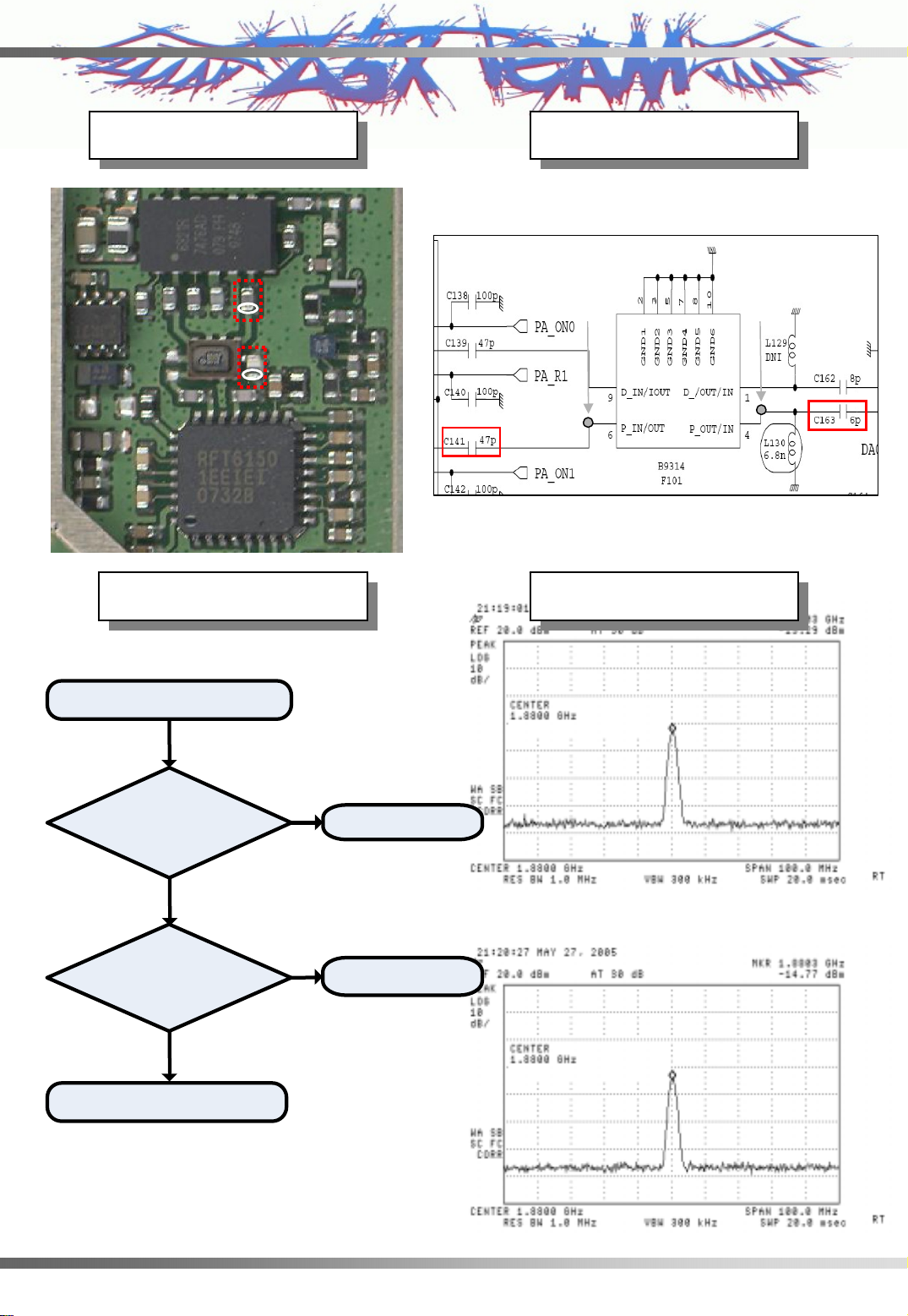
CX9100
4.2.2.4 Check RF Tx Dual SAW
Test Point
Test Point
U105
(Dual PAM)
F101
U109
(RFT6150)
Checking Flow
Checking Flow
P_OUT
P_IN
Circuit Diagram
Circuit Diagram
Waveform
Waveform
TP1TP2
Start
Check pin4(TP1)
at F101 . Referring to
Figure 4 .2 .2(g)
Is it similar ?
Check pin6(TP2)
at F101 . Referring to
Figure 4 .2 .2(h)
Is it similar ?
NO
Replace F 101
D_IN fed up with CW signal
P_IN
Check
U109(RFT6150)
YES
Z3X-BOX.COM
RF Tx Dual SAW is
OK
YES
Figure 4.2.2(g)
P_OUT
Copyright © 2007 LG Electronics. Inc. All right reserved
Only for training and service purposes
-82-
Figure 4.2.2(h)
LGE Internal Use Only
Page 84

CX9100
4.2.2.5 Check Dual PAM (PCS) circuit
Test Point
Test Point
VCCAVCC
U105
(Dual PAM)
VMODE RFIN_PCS
VBATT
RFOUT_PCS
VEN_PCS
Circuit Diagram
Circuit Diagram
TP1
PCS Tx
DCN Tx
TP4
Z3X-BOX.COM
TP2
TP3
Copyright © 2007 LG Electronics. Inc. All right reserved
Only for training and service purposes
-83-
LGE Internal Use Only
Page 85

CX9100
Checking Flow
Checking Flow
Start
Check pin 6 , 8 (TP1,2) at U105
Check if there is any major difference referring
To Figure 4.2.2(i) Is it similar?
YES
YES
PAM circuit is OK. See next page
Check pin 4 , 11
whether it is higher than 3.4V.
Check pin3(TP4) at U105(PA_R1 signal)
whether it is lower than 2.2V.
(TP3) at U105(Vcc)
YES
YES
Replace U105
Z3X-BOX.COM
RFIN_PCS fed up with CW signal
Waveform
Waveform
NO
Check Vcc line
Check PA_R1 line
NO
in low gain mode of PAM
Copyright © 2007 LG Electronics. Inc. All right reserved
Only for training and service purposes
Figure 4.2.2(i)
-84-
RFOUT_PCS
LGE Internal Use Only
Page 86

CX9100
4.2.2.6 Check Quinplexer (PCS)
Test Point
Test Point
PCS_TX_PORT
ANT_PORT
L132
DP100
(Quintplexer)
C116
U102
Circuit Diagram
Circuit Diagram
TP1
TP3
Z3X-BOX.COM
Copyright © 2007 LG Electronics. Inc. All right reserved
Only for training and service purposes
-85-
TP3
LGE Internal Use Only
Page 87

CX9100
Checking Flow
Checking Flow
Start
Check TP1 , TP2
at DP 100 . Referring to
Figure 4.2.2(j)
Is it similar ?
NO
Check TP2 , TP3
at DP 100 . Referring to
Figure 4.2.2(j)
Is it similar ?
NO
Check TP1 , TP3
at DP 100 . Referring to
Figure 4.2.2(j)
Is it similar ?
NO
Replace DP
100 , U102
Quintplexer,
Coupler are OK
YES
Replace U102
(coupler)
YES
Replace DP100
(Quintplexer)
YES
Waveform
Waveform
Z3X-BOX.COM
Tx Port
Figure 4.2.2(j)
Copyright © 2007 LG Electronics. Inc. All right reserved
Only for training and service purposes
-86-
ANT Port
LGE Internal Use Only
Page 88

CX9100
4.2.2.7 Check Mobile S/W
Test Point
Test Point
RF IN
RF OUT
Checking Flow
Checking Flow
Circuit Diagram
Circuit Diagram
TP2
TP1
Waveform
Waveform
Start
Check pin2(TP1) , 1(TP2)
at U100 . Referring to
Figure 4.2.2(k)
Is it similar ?
NO
Replace U100
RF_IN(ANT)
Mobile S/W is
OK
YES
Z3X-BOX.COM
RF_OUT(DUP)
Figure 4.2.2(k)
Copyright © 2007 LG Electronics. Inc. All right reserved
Only for training and service purposes
-87-
LGE Internal Use Only
Page 89

CX9100
4.3 Logic Part Trouble Shooting
4.3.1 Power
4.3.1.1 Power-On Trouble
Circuit Diagram
+VBATT
Circuit Diagram
+VPWR
+1.275V_MSMC
+1.85V_MSMP1
PS_HOLD
R409
L400
L401
C423
Test point
Test point
R431
+2.6V_MSMP2
R435
+2.6V_MSMA
+2.85V_TCXO
R437
PS_HOLD
+2.6V_MSMP2
Z3X-BOX.COM
+1.275V_MSMC
+1.85V_MSMP1
Copyright © 2007 LG Electronics. Inc. All right reserved
Only for training and service purposes
U401
+VBATT
+VPWR
+2.6V_MSMA
+2.85V_TCXO
-88-
U107
TCXO_OUT
LGE Internal Use Only
Page 90

CX9100
START
Checking Flow
Checking Flow
Check battery voltage > 3.4V
YES
Check the VPWR voltage > 3.4V
YES
Check the voltage of
the following port at U401
+1.275V_MSMC
+1.85V_MSMP1
+2.6V_MSMP2
+2.6V_MSMA
+2.85V_TCXO
YES
Is the frequency of TCXO (U107)
19.2Mhz?
NO
NO
NO
NO
Charge of Change Battery and try again
Confirm +VBATT Line
Replace PMIC (U401)
Check VPWR Voltage >3.4V
Replace TCXO (U107)
YES
download software
try again
Z3X-BOX.COM
Logic level at PS_HOLD
Of U401=High?
YES
Change the board
Copyright © 2007 LG Electronics. Inc. All right reserved
Only for training and service purposes
NO
-89-
Replace MSM (U202)
Does it work properly?
NO
Change the board
LGE Internal Use Only
Page 91

CX9100
4.3.1.2 Charging Trouble
+VBATT
Circuit Diagram
Circuit Diagram
USB_DETECT
+VBATT
VCHAR
CON603
Test point
Test point
+VCHAR
Z3X-BOX.COM
USB_DETECT
Copyright © 2007 LG Electronics. Inc. All right reserved
Only for training and service purposes
-90-
Q602
CON603
LGE Internal Use Only
Page 92

CX9100
START
Battery Change
Checking Flow
Checking Flow
Does it work properly
NO
Charging Connector CON603
Well-soldered?
YES
VCHAR (D602) =5V?
YES
USB_DECT(C646)
If connect USB Cable, 2.6V
If connect TA, 0V ?
YES
Check VBATT Voltage >3.4V
Z3X-BOX.COM
YES
YES
NO
NO
NO
NO
The battery may have the problem
Re-soldering CON603
The charging adaptor (TA) or USB cable(USB port
of computer) is out of order.
Replace Q602
Replace PMIC (U401)
download software
try again
Does it work properly
YES
Charging will operate properly
Copyright © 2007 LG Electronics. Inc. All right reserved
Only for training and service purposes
NO
-91-
The battery may have the problem
LGE Internal Use Only
Page 93

CX9100
4.3.2 LCD
4.3.2.1 LCD Trouble
Check point
- The assembly status of the LCD Module
- The assembly status of the main connector
- The Soldering of connector
Circuit Diagram
Circuit Diagram
D2[11]
D2[13]
D2[15]
SLCD_CS/
MLCD_CS/
MLCD_VSYNC
SLCD_VSYNC
D2[1]
D2[3]
D2[5]
D2[7]
D2[9]
F506
F506
ICVE10184E150R101FR
9
OUT1
8
OUT2
7
OUT3
6
OUT4
F509
F509
ICVE10184E150R101FR
9
OUT1
8
OUT2
7
OUT3
6
OUT4
F505
F505
ICVE10184E150R101FR
9
OUT1
8
OUT2
7
OUT3
6
OUT4
R511
F506
1
IN1
2
IN2
3
IN3
4
IN4
GND
5
10
F509
1
IN1
2
IN2
3
IN3
4
IN4
GND
5
10
F505
1
IN1
2
IN2
3
IN3
4
IN4
GND
5
10
SUB_KEY_LED_EN
FOLDER_ON_SW
LCD_IFMODE
KYPD[1]
KYPD[3]
KYPD[5]
KYPD[7]
KYPD[9]
KYPD[11]
KYPD[13]
KYPD[15]
KYPD[17]
LCD_BL_OUT
MLED5
MLED4
MLED3
MLED2
MLED1
R509
OE2/
0
R510
DNI
100
33p
33p
33p
0.1u
33p
C504
C507
C505
C510
C503 33p
C506 33p
C544 ICVS0505500FR
C546
CON501
AXT570124
1
70
2
69
3
68
4
67
5
66
6
65
7
64
8
63
9
DUMMY
71 7372 74
62
61
60
59
58
57
56
55
54
53
52
51
50
49
48
47
46
45
44
43
42
41
40
39
38
37
36
10
11
12
13
14
15
16
17
18
19
20
21
22
23
24
25
26
27
28
29
30
31
32
33
34
35
33p
10n
C501
C502
Test point
Test point
ICVS0505500FR
1u
C545
C518
SPK_R+
SPK_R-
SPK_LSPK_L+
82n
L501
L502
ICVS0505500FR
ICVS0505500FR
ICVS0505500FR
0.1u
C500
ICVS0505500FR
C512
C513
C516
C517
RCV+
82n
RCV-
SLED1
SLED2
+1.85V_MSMP1
+2.8V_LCD
LCD_ID
+VPWR
+3.0V_MOTOR
33p
33p
0.1u
C508
C509
C520 0.1u
C519
F504
ICVE10184E150R101FR
9
OUT1
8
OUT2
7
OUT3
6
OUT4
F508
ICVE10184E150R101FR
9
OUT1
8
OUT2
7
OUT3
6
OUT4
GND
F503
ICVE10184E150R101FR
9
OUT1
8
OUT2
7
OUT3
6
OUT4
GND
F504
F504
1
IN1
D2[0]
2
IN2
D2[2]
3
IN3
D2[4]
4
IN4
D2[6]
GND
5
10
F508
F508
1
IN1
D2[8]
2
IN2
D2[10]
3
IN3
D2[12]
4
IN4
D2[14]
5
10
F503
F503
1
IN1
WE2/
2
IN2
LCD_RS
3
IN3
SLCD_RESET/
4
IN4
MLCD_RESET/
5
10
Z3X-BOX.COM
F503
F508
F504
Copyright © 2007 LG Electronics. Inc. All right reserved
Only for training and service purposes
-92-
F505
F509
F506
LGE Internal Use Only
Page 94

CX9100
START
Checking Flow
Checking Flow
Does LCD work properly
YES
Check the LCD FPCB
YES
Check the C431 (2.85V) and C406(1.85V)
of PMIC Voltage
YES
Check the Control Signal LCD Data[0:15]
Reset/, LCD_CS, LCD_WE/
NO
NO
NO
NO
Change the LCD Module
Change the LCD FPCB
Replace PMIC ( U401 )
Check the LCD Signal Line
( F503,F504,F505,F506,F508,F509)
YES
Z3X-BOX.COM
Check CON 501 soldering
YES
LCD Display will work properly
Copyright © 2007 LG Electronics. Inc. All right reserved
Only for training and service purposes
NO
-93-
Re-solder CON 501
LGE Internal Use Only
Page 95

CX9100
4.3.3 Camera
4.3.3.1 Camera Trouble
Circuit Diagram
Circuit Diagram
Z3X-BOX.COM
Copyright © 2007 LG Electronics. Inc. All right reserved
Only for training and service purposes
Test point
Test point
-94-
LGE Internal Use Only
Page 96

CX9100
Checking Flow
Checking Flow
Z3X-BOX.COM
Copyright © 2007 LG Electronics. Inc. All right reserved
Only for training and service purposes
-95-
LGE Internal Use Only
Page 97

CX9100
Camera Trouble
Circuit Diagram
Circuit Diagram
Z3X-BOX.COM
Copyright © 2007 LG Electronics. Inc. All right reserved
Only for training and service purposes
-96-
LGE Internal Use Only
Page 98

CX9100
Test point
Test point
Checking Flow
Checking Flow
Z3X-BOX.COM
Copyright © 2007 LG Electronics. Inc. All right reserved
Only for training and service purposes
-97-
LGE Internal Use Only
Page 99

CX9100
4.3.4 Audio
4.3.4.1 Speaker Trouble
Circuit Diagram
Circuit Diagram
R301 HPH_L
R302 HPH_R
Z3X-BOX.COM
U301 Audio Amp
Copyright © 2007 LG Electronics. Inc. All right reserved
Only for training and service purposes
Test point
Test point
R306 VPWR+
-98-
C315 SPK_R+/-
C314 SPK_L+/-
LGE Internal Use Only
Page 100

CX9100
START
Checking Flow
Checking Flow
Voltage at R306 is
about 3.4~4.2V
YES
Check audio signal at R301, R302
YES
Check audio signal at C314, C315
YES
Check the state of contact of speaker
YES
Speakerwill work properly
NO
NO
NO
NO
Check the Battery Voltage
Check the soldering at
R301, R302
YES
Check the soldering at
C314, C315
YES
Replace speaker
NO
NO
Replace MSM or Main Board
Resolder R301, R302
Replace U301
Resolder C314, C315
Z3X-BOX.COM
Copyright © 2007 LG Electronics. Inc. All right reserved
Only for training and service purposes
-99-
LGE Internal Use Only
 Loading...