

Page 1
Features of CX830
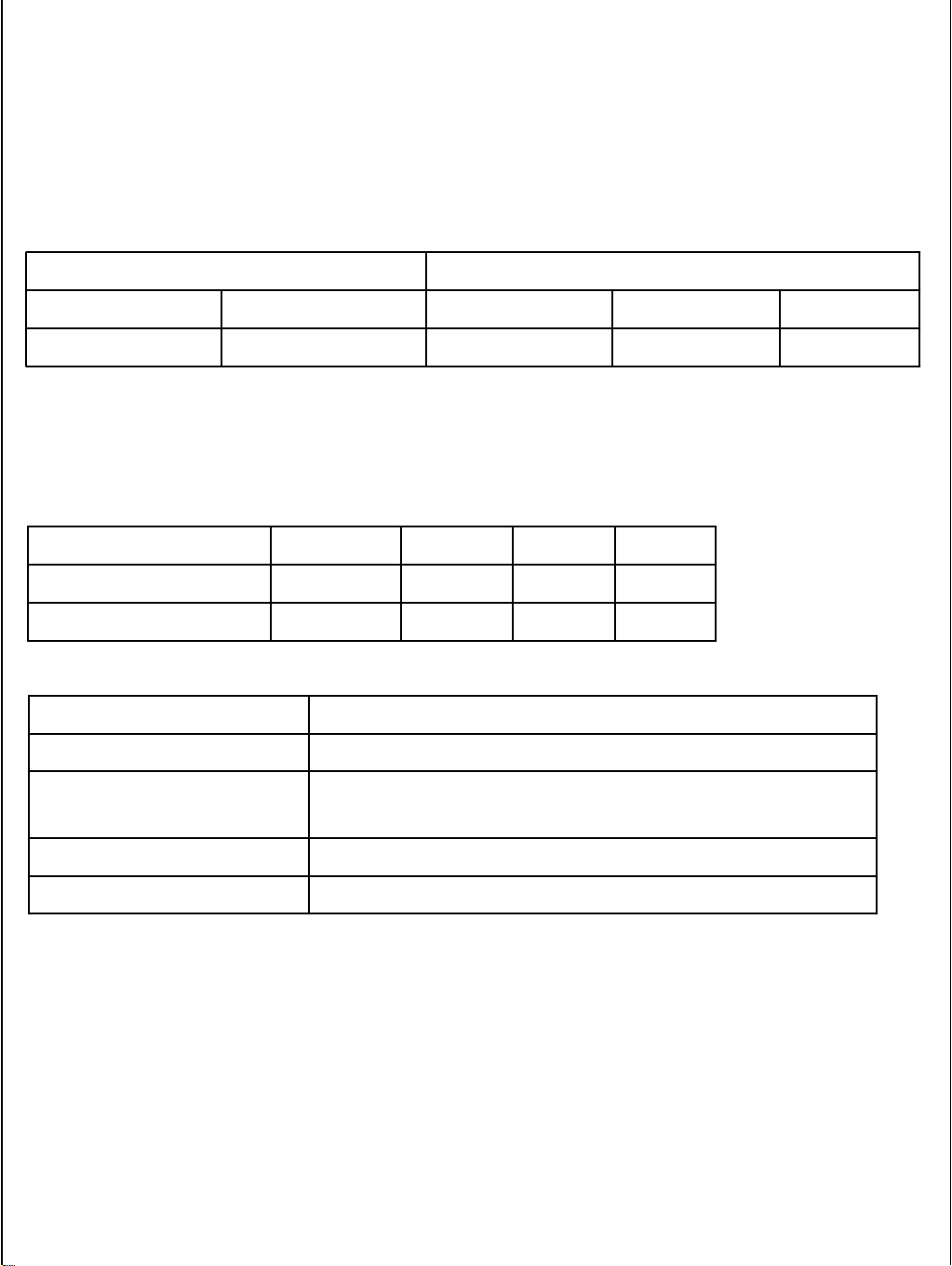
1. Wave Type
CELLULAR : G7W
●
PCS: G7W
●
2. Frequency Scope
Receive Frequency (MHz)Transmit Frequency (MHz)
3. Rated Output Power : CELLULAR = 0.25W
PCS = 0.25W
4. Output Conversion Method : This is possible by correcting the key board channel.
5. Voltage and Current Value of Termination Part Amplifier (Catalogue included)
PowerCurrentVoltagePart NameMODE
0.25W400mA4.2VAWT6307RCELLULAR
GPSPCSCELLULARPCSCELLULAR
1575.421930~1990869.82~893.191850~1910824.82 ~ 848.19
6. Functions of Major Semi-Conductors
Terminal operation control and digital signal processing MSM6500
Memory MCP
(TY9000A000BMGF)
7. Frequency Stability
CELLULAR : ±0.5PPM
●
● PCS : ±0.1PPM
Z3X-BOX.COM
Flash Memory (1024Mbit) + SDRAM (512Mbit)
Storing of terminal operation program
Converts Rx RF signal to baseband signalRFR6500
Converts baseband signal to Tx RF signalRFT6150
0.25W400mA4.2VAWT6308RPCS
FunctionClassification
Page 2

CDMA Mobile Subscriber Unit
CX830
SERVICE MANUAL
SERVICE MANUAL
DUAL BAND CDMA
[PCS/Cellular/w/GPS]
CDMA MOBILE PHONE
Z3X-BOX.COM
Page 3

Table of Contents
General Introduction……………………………………………………………………………...3
CHAPTER 1. System Introduction
1. CDMA Abstract…….………………………………………………………………….…….…..4
2. Features and Advantages of CDMA Mobile Phone…………....................................... . 5
3. Structure and Functions of Dual-band CDMA Mobile Phone……………………….…..8
4. Specification……………………………………………………………………………………..9
5. Installation………………………………………………………………………………………14
CHPATER 2. NAM Input Method
1. NAM Program Method and Telephone Number Inputting Method……………………16
CHAPTER 3. Circuit Description
1. RF Transmit/Receive Part……………………………………………………………….……26
2. Digital/Voice Processing Part……………………………………………………………….32
CHAPTER 4. Trouble Shooting………………………………………………………………...37
CHAPTER 5. Safety……………………………………………………………………..………133
CHAPTER 6. Glossary……………………………………………………………………….…136
APPENDIX…………………………………………………………………………………...……148
Z3X-BOX.COM
Page 4

General Introduction
General Introduction
The CX830 phone has been designed to operate on the latest digital mobile communication technology, Code
Division Multiple Access (CDMA). This CDMA digital technology has greatly enhanced voice clarity and can
provide a variety of advanced features. Currently, CDMA mobile communication technology has been
commercially used in Cellular and Personal Communication Service (PCS). The difference between them is the
operating frequency spectrum. Cellular uses 800MHz and PCS uses 1.9GHz. The CX830 support GPS Mode, we
usually call it tri-band phone. Also, CX830 works on Advanced Mobile Phone Service (S-GPS). We call it dualmode phone. If one of the Cellular, PCS base stations is located nearby, Call fail rate of triple-mode phone is less
than dual-mode phone or single-mode phone.
The CDMA technology adopts DSSS (Direct Sequence Spread Spectrum). This feature of DSSS enables the phone
to keep communication from being crossed and to use one frequency channel by multiple users in the same specific
area, resulting that it increases the capacity 1 0 times more compared with that in the analog mode currently used.
Soft/Softer Handoff, Hard Handoff, and Dynamic RF power Control technologies are combined into this phone to
reduce the call being interrupted in a middle of talking over the phone.
Cellular and PCS CDMA network consists of MSO (Mobile Switching Office), BSC (Base Station Controller), BTS
(Base station Transmission System), and MS (Mobile Station). The following table lists some major CDMA
Standards.
Basic air interface
Network
Service
Performance
* TSB –74: Protocol between an IS-95A system and ANSI J-STD-008
TIA/EIA/IS-95-A/B/C
ANSI J-STD-008
TIA/EIA/IS-634
TIA/EIA/IS/651
TIA/EIA/IS-41-C
TIA/EIA/IS-124
TIA/EIA/IS-96-B
TIA/EIA/IS-99
TIA/EIA/IS-637
TIA/EIA/IS-657
TIA/EIA/IS-97
Z3X-BOX.COM
TIA/EIA/IS-98
ANSI J-STD-018
ANSI J-STD-019
TIA/EIA/IS-125
Protocol between MS and BTS for Cellular & AMPS
Protocol between MS and BTS for PCS
DescriptionDesignatorCDMA Standard
MAS-BS
PCSC-RS
Intersystem operations
Nom-signaling data comm.
Speech CODEC
Assign data and fax
Short message service
Packet data
Cellular base station
Cellular mobile station
PCS personal station
PCS base station
Speech CODEC
Page 5

Chapter1. System Introduction
Chapter1. System Introduction
1. CDMA Abstract
The CDMA mobile communication system has a channel hand-off function that is used for collecting the information
on the locations and movements of mobile telephones from the cell site by automatically controlling several cell site
through the setup of data transmission routes, and then enabling one switching system to carry out the automatic
remote adjustment. This is to maintain continuously the call state through the automatic location confirmation and
automatic radio channel conversion when the busy subscriber moves from the service area of one cell site to that of
another by using automatic location confirmation and automatic radio channel conversion functions. The call state
can be maintained continuously by the information exchange between switching systems when the busy subscriber
moves from one Cellular system area to the other Cellular system area.
In the Cellular system, the cell site is a small-sized low output type and utilizes a frequency allocation system that
considers mutual interference, in an effort to enable the re-use of corresponding frequency from a cell site separated
more than a certain distance.
Unlike the time division multiple access (TDMA) or frequency division multiple access (FDMA) used in the band
limited environment, the Code Division Multiple Access (CDMA) system which is one of digital Cellular systems is
a multi-access technology under the interference limited environment. It can process more number of subscribers
compared to other systems (TDMA system has the processing capacity three times greater than the existing FDMA
system whereas CDMA system, about 12~15 times of that of the existing system).
CDMA system can be explained as follows; TDMA or CDMA can be used to enable each person to talk alternately
or provide a separate room for each person when two persons desire to talk with each other at the same time, whereas
FDMA can be used to enable one person to talk in soprano, whereas the other in bass (one of the two talkers can
carry out synchronization for hearing in case there is a bandpass filter function in the area of the hearer). Another
available method is to make two persons to sing in different languages at the same time, space, and frequency when
wishing to let the audience hear the singing without being confused. This is the characteristic of CDMA.
On the other hand, when employing the CDMA technology, each signal has a different pseudo-random binary
sequence used to spread the spectrum of carrier. A great number of CDMA signals share the same frequency
spectrum. In the perspective of frequency area or time area, several CDMA signals are overlapped. Among these
types of signals, only desired signal energy is selected and received through the use of pre-determined binary
sequence; desired signals can be separated, and then received with the correlators used for recovering the spectrum
into its original state. At this time, the spectrums of other signals that have different codes are not recovered into its
original state, and appears as the self-interference of the system.
Z3X-BOX.COM
Page 6

2. Features and Advantages of CDMA Mobile Phone
2.1 Various Types of Diversities
When employing the narrow band modulation (30kHz band) that is the same as the analog FM modulation system
used in the existing Cellular system, the multi-paths of radio waves create a serious fading. However, in the CDMA
broadband modulation (1.25MHz band), three types of diversities (time, frequency, and space) are used to reduce
serious fading problems generated from radio channels in order to obtain high-quality calls.
Time diversity can be obtained through the use of code interleaving and error correction code whereas frequency
diversity can be obtained by spreading signal energy to wider frequency band. The fading related to normal
frequency can affect the normal 200~300KHz among signal bands and accordingly, serious effect can be avoided.
Moreover, space diversity (also called path diversity) can be realized with the following three types of methods.
First, it can be obtained by the duplication of cell site receive antenna. Second, it can be obtained through the use of
multi-signal processing device that receives a transmit signal having each different transmission delay time and then,
combines them. Third, it can be obtained through the multiple cell site connection (Soft Handoff) that connects the
mobile station with more than two cell sites at the same time.
2.2 Power Control
The CDMA system utilizes the forward (from a base station to mobile stations) and backward (from the mobile
station to the base station) power control in order to increase the call processing capacity and obtain high-quality calls.
In case the originating signals of mobile stations are received by the cell site in the minimum call quality level (signal
to interference) through the use of transmit power co ntrol on all the mobile stations, the system capacity can be
maximized. If the signal power of mobile station is received too strong, the performance of that mobile station is
improved. However, because of this, the interference on other mobile stations using the same channel is increased
and accordingly, the call quality of other subscribers is reduced unless the maximum accommodation capacity is
reduced.
In the CDMA system, forward power control, backward open loop power control, and closed loop power control
methods are used. The forward power control is carried out in the cell site to reduce the transmit power on mobile
stations less affected by the multi-path fading and shadow phenomenon and the interference of other cell sites when
the mobile station is not engaged in the call or is relatively nearer to the corresponding cell site. This is also used to
provide additional power to mobile stations having high call error rates, located in bad receptio n areas or far away
from the cell site.
The backward open loop power control is carried out in a corresponding mobile station; the mobile station measures
power received from the cell site and then, reversely increases/decreases transmit power in order to compensate
channel changes caused by the forward link path loss and terrain characteristics in relation to the mobile station in the
cell site. By doing so, all the mobile transmit signals received by the base station have same strength.
Moreover, the backward closed loop power control used by the mobile station is performed to control power using
the commands issued out by the cell site. The cell site receives the signal of each corr esponding mobile station and
compares this with the pre-set threshold value and then, issues ou t power in crease/decrease commands to the
corresponding mobile station every 1.25msec (800 times per second). By doing so, the gain tolerance and the
different radio propagation loss on the forward/backward link are complemented.
Z3X-BOX.COM
Page 7

2.3 Voice Encoder and Variable Data Speed
The bi-directional voice service having variable data speed provides voice communication which employs voice
encoder algorithm having power variable data rate between the base station and the mobile station. On the other hand,
the transmit voice encoder performs voice sampling and then, creates encoded voice packets to be sent out to the
receive voice encoder, whereas the receive voice encoder demodulates the received voice packets into voice samples.
One of the two voice encoders described in the above is selected for use depending on inputted automatic conditions
and message/data; both of them utilize four-stage frames of 9600, 4800, 2400, and 1200 bits per second for Cellular
and 14400,7200,3600,1800 bits per second for PCS, so PCS provide relatively better voice quality (almost twice
better than the existing cellular system). In addition, this type of variable voice encoder utilizes adaptive threshold
values on selecting required data rate. It is adjusted in accordance with the size of background noise and the data rate
is increased to high rate only when the voice of caller is inputted.
Therefore, background noise is suppressed and high-quality voice transmission is possible under the environment
experiencing serious noise. In addition, in case the caller does not talk, data transmission rate is reduced so that the
transmission is carried out in low energy. This will reduce the interference on other CDMA signals and as a result,
improve system performance (capacity increased by about two times).
2.4 Protecting Call Confidentiality
Voice privacy is provided in the CDMA system by means of the private long code mask used for PN spreading.
Voice privacy can be applied on the traffic channels only. All calls are initiated using the public long code mask for
PN spreading. The mobile station user may request voice privacy during call setup using the origination message or
page response message, and during traffic channel operation using the long code transition request order.
The Transition to private long code mask will not be performed if authentication is not performed. To initiate a
transition to the private or public long code mask, either the base station or the mobile station send s a long code
transition request order on the traffic channel.
2.5 Soft Handoff
A handoff in which the mobile station commences communications with a new base station without interrupting
communications with the old base station. Soft handoff can only be used between CDMA channels having identical
frequency assignments.
Z3X-BOX.COM
2.6 Frequency Re-Use and Sector Segmentation
Unlike the existing analog Cellular system, the CDMA system can reuse the same frequency at the adjacent cell.
there is no need to prepare a separate frequency plan. Total interference generated on mobile station signals received
from the cell site is the sum of interference generated from other mobile stations in the same cell site and interference
generated from the mobile station of adjacent cell site. That is, each mobile station signal generates interference in
relation to the signals of all the other mobile stations.
Page 8

Total interference from all the adjacent cell sites is the ratio of interference from all the cell sites versus total
interference from other mobile stations in the same cell site (about 65%). In the case of directional cell site, one cell
normally uses a 120°sector antenna in order to divide the sector into three. In this case, each antenna is used only for
1/3 of mobile stations in the cell site and accordingly, interference is reduced by 1/3 on the average and the capacity
that can be supported by the entire system is increased by three times.
2.7 Soft Capacity
The subscriber capacity of the CDMA system is flexible depending on the relation between the number of users and
service classes. For example, the system operator can increase the number of channels available for use during the
busy hour despite the drop in call quality. This type of function requires 40% of normal call channels in the standby
mode during the handoff, in an effort to avoid call disconnection resulting from the lack of channels.
In addition, in the CDMA system, services and service charges are classified further into different classes so that
more transmit power can be allocated to high class service users for easier call set-up; they can also be given higher
priority of using hand-off function than the general users.
Z3X-BOX.COM
Page 9

3. Structure and Functions of tri-band CDMA Mobile Phone
The hardware structure of CDMA mobile phone is made up of radio frequency (RF) part and logic part. The RF part
is composed of Receiver part (Rx), Transmitter part (Tx) and Local part (LO). For the purp ose of operating on triband, It is necessary dual Tx path, tri Rx path, dual PLL and switching system for band selection. The mobile phone
antenna is connected with the frequency separator which divide antenna input/output signals between Cellular
frequency band (824~894 MHz) and PCS frequency band (1850~1990MHz). Each separated path is linked with the
Cellular duplexer and PCS duplexer. Duplexer carries out separating Rx band and Tx band. The Rx signals from the
antenna are converted into intermediate frequency(IF) band by the frequency synthesizer and frequency down
converter. And then, pass SAW filter which is a band pass filter for removing out image frequency. The IF output
signals that have been filtered is converted into digital signals via Analog-to-Digital Converter (ADC). In front of the
ADC, switching system is required to choose which band path should be open. The digital signals send to 5
correlators in each CDMA de-modulator. Of these, one is called a searcher whereas the remaining 4 are called data
receivers (fingers). Digitalized IF signals include a great number of call signals that have been sent out by the
adjacent cells. These signals are detected with pseudo-noise sequence (PN Sequence). Signal to interference ratio
(C/I) on signals that match the desired PN sequence are increased through this type of correlation detection process,
but other signals obtain processing gain by not increasing the ratio. The carrier wave of pilot channel from the cell
site most adjacently located is demodulated in order to obtain the sequence of encoded data symbols. During the
operation with one cell site, the searcher searches ou t multi-paths in ac cordance with terrain and building reflections.
On three data receivers, the most powerful 3 paths are allocated for the parallel tracing and receiving. Fading
resistance can be improved a great deal by obtaining the diversity combined output for de-modulation. Moreover, the
searcher can be used to determine the most powerful path from the cell sites even during the soft handoff between the
two cell sites. Moreover, 3 data receivers are allocated in order to carry out the de-modulation of these paths. Output
data that has been demodulated changes the data string in the combined data row as in the case of original
signals(deinterleaving), and then, are demodulated by the forward error correction decoder which uses the Viterbi
algorithm.
Mobile station user information send out from the mobile station to the cell site pass through the digital voice
encoder via a mike. Then, they are encoded and forward errors are corrected through the use of convolution encoder.
Then, the order of code rows is changed in accordance with a certain regulation in order to remove any errors in the
interleaver. Symbols made through the above process are spread after being loaded onto PN carrier waves. At this
time, PN sequence is selected by each address designated in each call.
Signals that have been code spread as above are digital modulated (QPSK) and then, power controlled at the
automatic gain control amplifier (AGC Amp). Then, they are converted into RF band by the frequency synthesizer
synchronizing these signals to proper output frequencies.
Transmit signals obtained pass through the duplexer filter and then, are sent out to the cell site via the antenna.
Z3X-BOX.COM
Page 10
4. Specification
4.1 General Specification
4.1.1 Transmit/Receive Frequency Interval :
1)CELLULAR : 45 MHz
2)PCS : 80 MHz
4.1.2 Number of Channels (Channel Bandwidth)
1)CELLULAR : 20 Channels
2) PCS : 48 Channels
4.1.3 Operating Voltage : DC 3.3~4.2V
4.1.4 Battery Power Consumption : DC 3.7V
MAX POWERIDLESLEEP
700 mA (24 dBm)110~180mA1.1 mA CELLULAR
700 mA (24 dBm)120~180 mA1.1 mAPCS
4.1.5 Operating Temperature : -0°C ~ +60°C
4.1.6 Frequency Stability
1)CDMA : ±0.5PPM
2)PCS : ±0.1PPM
4.1.7 Antenna : Press Type (PIFA), 50
4.1.8 Size and Weight
1)Size : 101.87(H) * 52(W) * 14.95(D) mm
2)Weight : 126.8 g (Approximately with standard battery)
4.1.9 Channel Spacing
Z3X-BOX.COM
1)CELLULAR : 1.25MHz
2)PCS: 1.25 MHz
4.1.10 Battery Type, Capacity and Operating Time.
Standby Time
Unit = Hours : Minutes
Standard (800mAh)
About 165 Hours (SCI=2)CELLULAR
About 165 Hours (SCI=2)PCS
Talk time
140 Minutes (-92dBm input)CELLULAR
140 Minutes (-92dBm input)PCS
Page 11

4.2 Receive Specification
4.2.1 Frequency Range
CELLULAR : 869.820 MHz ~ 893.190 MHz
PCS : 1930 MHz ~ 1990 MHz
GPS : 1575.42 MHz
4.2.2 Local Oscillating Frequency Range :
CELLULAR : 1738.08MHz ~ 1787.94MHz
PCS : 1715.56MHz ∼ 1768.89MHz
GPS : 3150.84MHz
4.2.3 Sensitivity
CELLULAR : -104dBm (C/N 12dB or more)
PCS : -104dBm (C/N 12dB or more)
GPS : -148.5dBm (without SA mode)
4.2.4 Selectivity
CELLULAR : 3dB C/N Degration (With Fch±1.25 kHz : -30dBm)
PCS : 3dB C/N Degration (With Fch±1.25 kHz : -30dBm)
4.2.5 Spurious Wave Suppression : Maximum of -80dB
4.2.6 CDMA Input Signal Range
Dynamic area of more than -104~ -25 dB: 79dB at the 1.23MHz band.
4.3 Transmit Specification
4.3.1 Frequency Range
CELLULAR : 824.820MHz ~ 848.190MHz
PCS : 1850 MHz ~ 1910 MHz
4.3.2 Output Power
CELLULAR : 0.224W
PCS: 0.224W
4.3.3 Interference Rejection
Single Tone : -30dBm at 900 kHz (CELLULAR), -30dBm at 1.25MHz(PCS)
Two Tone : -43dBm at 900 kHz & 1700kHz(CELLULAR), -43dBm at 1.25 MHz & 2.05 MHz (PCS)
Z3X-BOX.COM
Page 12
4.3.11 CDMA TX Frequency Deviation :
1) CELLULAR: +300Hz or less
2) PCS: ± 150Hz
4.3.12 CDMA TX Conducted Spurious Emissions
1) CELLULAR: 900kHz : - 42 dBc/30kHz below
1.98MHz : - 54 dBc/30kHz below
2) PCS: 1.25MHz: - 42 dBc/30kHz below
1.98MHz : - 50 dBc/30kHz below
4.3.13 CDMA Minimum TX Power Control
1) CELLULAR: - 50dBm below
2) PCS: -50dBm below
4.4 MS (Mobile Station) Transmitter Frequency
4.4.1 CELLULAR mode
1011
29
70
111
152
193
234
275
316
363
4.4.2 PCS mode
Ch #
Center Freq. (MHz)Ch #Center Freq. (MHz)Ch #
824.640
825.870
827.100
828.330
829.560
830.790
832.020
833.250
834.480
835.890
Ch #Center Freq
(MHz)
Z3X-BOX.COM
404
445
486
527
568
609
650
697
738
779
Ch #Center Freq
(MHz)
837.120
838.350
839.580
840.810
842.040
843.270
844.500
845.910
847.140
848.370
Center Freq
(MHz)
1891.25 8251871.25 4251851.25 25
1892.50 8501872.50 4501852.50 50
1893.75 8751873.75 4751853.75 75
1895.00 9001875.00 5001855.00 100
1896.25 9251876.25 5251856.25 125
1897.50 9501877.50 5501857.50 150
1898.75 9751878.75 5751858.75 175
Page 13
4.5 MS (Mobile Station) Receiver Frequency
4.5.1 CELLULAR mode
1900.00 10001880.00 6001860.00 200
1901.25 10251881.25 6251861.25 225
1902.50 10501882.50 6501862.50 250
1903.75 10751883.75 6751863.75 275
1905.00 11001885.00 7001865.00 300
1906.25 11251886.25 7251866.25 325
1907.50 11501887.50 7501867.50 350
1908.75 11751888.75 7751868.75 375
Center Freq. (MHz)Ch. #Center Freq. (MHz)Ch. #
1011
29
70
111
152
193
234
275
316
363
4.5.2 PCS mode
869.640
870.870
872.100
873.330
874.560
875.790
877.020
878.250
879.480
880.890
Ch #Center Freq
(MHz)Ch #
404
445
486
527
568
609
650
697
738
779
Ch #Center Freq
(MHz)
882.120
883.350
884.580
885.810
887.040
888.270
889.500
890.910
892.140
893.370
Center Freq
(MHz)
1971.25 8251951.25 4251931.25 25
1972.50 8501952.50 4501932.50 50
1973.75 8751953.75 4751933.75 75
Z3X-BOX.COM
1975.00 9001955.00 5001935.00 100
1976.25 9251956.25 5251936.25 125
1977.50 9501957.50 5501937.50 150
1978.75 9751958.75 5751938.75 175
1980.00 10001960.00 6001940.00 200
1981.25 10251961.25 6251941.25 225
Page 14

4.5.3 GPS mode : 1575.42 MHz
4.5.4 Bluetooth mode : 2400 MHz ~ 2483.5 MHz
4.6 AC Adaptor : See Appendix
4.7 Cigar Lighter Charger : See Appendix
1982.50 10501962.50 6501942.50 250
1983.75 10751963.75 6751943.75 275
1985.00 11001965.00 7001945.00 300
1986.25 11251966.25 7251946.25 325
1987.50 11501967.50 7501947.50 350
1988.75 11751968.75 7751948.75 375
Z3X-BOX.COM
Page 15

5. Installation
5.1 Installing a Battery Pack
1) The Battery pack is keyed so it can only fit one way. Align the groove in the battery pa ck with the rail on the back
of the phone until the battery pack rests flush with the back of the phone.
2) Slide the battery pack forward until you hear a “click”, which locks the battery in place.
5.2 For Adapter Use
1) Plug the adapter into a wall outlet. The adapter can be operated from a 110V source. When AC power is connected
to the adapter.
2) Insert the adapter IO plug into the phone with the installed battery pack.
Red light indicates battery is being charged.. Green light indicates battery is fully charged.
5.3 For Mobile Mount
5.3.1 Installation Position
In order to reduce echo sound when using the Hands-Free Kit, make sure that the speaker and microphone are not
facing each other and keep microphone a generous distance from the speaker.
5.3.2 Cradle Installation
Choose an appropriate flat surface where the un it will not interface with driver’s movement or passenger’s comfort.
The driver/user should be able to access the phone with ease. Using the four self-tapping screws provided, mount the
supplied bracket on the selected area. Then with the four machine screws provided, mount the counterpart on the
reverse side of the reverse side of the cradle. Secure the two brackets firmly together by using the two bracket joint
screws provide. The distance between the cradle and the interface box must not exceed the length of the main cable.
5.3.3 Interface Box
Choose an appropriate flat surface ( somewhere under the dash on the passenger side is preferred ) and mount the IB
bracket with the four self-tapping screws provided. Clip the IB into the IB bracket.
5.3.4. Microphone Installation
Install the microphone either by clipping I onto the sunvisor (driver’s side) or by attaching it to door post (driver’s
side), using a velcro adhesive tape (not included).
Z3X-BOX.COM
5.3.5 Cable Connections
Page 16

5.3.5.1 Power and Ignition Cables
Connect the red wire to the car battery positive terminal and the black wire to the car ground. Connect the green wire
to the car ignition sensor terminal. ( In order to operate HFK please make sure to connect green wire to ignition
sensor terminal.) Connect the kit’s power cable connector to the interface box power receptacle.
5.3.5.2 Antenna Cable Connection
Connect the antenna coupler cable connector from the cradle to the external antenna connector. ( Antenna is not
included.)
Z3X-BOX.COM
Page 17

CHAPTER 2. NAM Input Method
CHAPTER 2. NAM Input Method
(Inputting of telephone numbers included)
(Inputting of telephone numbers included)
1. NAM Programming Method and Telephone Number Input Method
1. Press ##2342# (##CDG2#)
2. Enter Service Code “000000”.
3. You can see following Menu
4. Press “1” key or Touch ‘Service Program’ list.
You can see following submenus.
Z3X-BOX.COM
4-1) Press “1” key or Touch ‘Reset Phone’ list.
You can reset the phone
Page 18

4-2) Press “2” key or Touch ‘Mobile Phone #’ list.
Input Mobile Phone Number and press softkey “OK” to save the change.
Press softkey “Í” to go back to the list.
4-3) Press “3” key or Touch ‘Home SID’ list.
Input the Home SID and press softkey “OK” to save the change.
Press softkey “Í” to go back to the list.
4-4) Press “4” key or Touch ‘Advanced’ list.
There are eleven submenus as below.
4-4.1) Press “1” key or Touch ‘MCC’ list.
Input the Mobile Country Code and press softkey “OK” to save the change.
Press softkey “Í” to go back to the list.
Z3X-BOX.COM
Page 19

4-4.2) Press “2” key or Touch ‘NMSI’ list.
Input the NMSI and press softkey “OK” to save the change.
Press softkey “Í” to go back to the list.
4-4.3) Press “3” key or Touch ‘True MCC’ list.
Input the True MCC and press softkey “OK” to save the change.
Press softkey “Í” to go back to the list.
4-4.4) Press “4” key or Touch ‘True IMSI NMSI’ list.
Input the True IMSI NMSI and press softkey “OK” to save the change.
Press softkey “Í” to go back to the list.
Z3X-BOX.COM
Page 20

4-4.5) Press “5” key or Touch ‘Home NID’ list.
Input the Home NID and press softkey “OK” to save the change.
Press softkey “Í” to go back to the list.
4-4.6) Press “6” key or Touch ‘Home Sys Reg’ list.
Select one what you want and touch it.
Press softkey “Í” to go back to the list.
4-4.7) Press “7” key or Touch ‘Forn SID Reg’ list.
Select one what you want and touch it.
Press softkey “Í” to go back to the list.
Z3X-BOX.COM
Page 21

4-4.8) Press “8” key or Touch ‘Forn NID Reg’ list.
Select one what you want and touch it.
Press softkey “Í” to go back to the list.
4-4.9) Press “9” key or Touch ‘CDMA Preferred CH’ list.
Select one what you want to edit, and touch it.
Press softkey “Í” to go back to the list.
4-4.10) Press “0” key or Touch ‘Slot Cycle Idx’ list.
Input the Slot Cycle and press softkey “OK” to save the change.
Press softkey “Í” to go back to the list.
Z3X-BOX.COM
Page 22

4-4.11) Press “*” key or Touch ‘Acc Ovld Class’ list.
You can see the Access Overload Class that is automatically set accord ing to IMSI_M
Press softkey “Í” to go back to the list.
Z3X-BOX.COM
Page 23

CHAPTER 3. Circuit Description
CHAPTER 3. Circuit Description
1. RF Transmit/Receive Part
1.1 Overview
The TX and RX part employs the Direct-Conversion system. The TX and RX frequencies are respectively
824.04~848.97 and 869.04~893.97 for cellular and 1850~1910 and 1930~1990 for PCS. The block diagram is shown
in [Figure 1-1]. CDMA RF signals received through the antenna are separated by the Diplexer.
RF Signal fed into the low noise amplifier in RFR6500(LNA) through the duplexer. Then, they are fed into Mixer in
RFR6500. In RFR6500, the RF signal is changed into baseband signal directly. Then, this signal is changed into
digital signal by the analog to digital converter (ADC, A/D Converter), and the digital circuit part of the
MSM(Mobile Station Modem) 6500 processes the data from ADC. The digital processing part is a demodulator.
In the case of transmission, RFT6150 receives OQPSK-modulated analog signal from the MSM6500.
The RFT6150 connects directly with MSM6500 using an analog baseband interface. In RFT6150, the baseband
quadrature signals are upconverted to the Cellular or PCS frequency bands and amplified to provide signal drive
capability to the power amp.
After that, the RF signal is amplified by the Power Amp in order to have enough power for radiation. Finally, the RF
signal is sent out to the cell site via the antenna after going through the duplexer.
Z3X-BOX.COM
Page 24
[Figure 1-1] RF Block Diagram of CX830
DP1000
U1001
F1000
F1002
F1001
U1006
U1009
F1003
U1008
F1004
U1007
Z3X-BOX.COM
Page 25
1.2 Description of RX Part Circuit
1.2.1 Quintiplexer(DP1000)
The Quintplexer combines PCS, and Cellular duplexer functions with a GPS filter. Each duplexer consists of the Rx
bandpass filter (BPF) and the Tx BPF which has the function of separating Tx and Rx signals in the full duplex
system for using the common antenna. The Tx part BPF is used to suppress noises and spurious out of the Tx
frequency band. The Rx BPF is used to receive only Rx signal coming from the antenna, which is usually called
preselector. It’s main function is to limit the bandwidth of spectrum reaching the LNA and mixer, attenuate receiver
spurious response and suppress local oscillator energy. As a result frequency sensitivity and selectivity of mobile
phone increase. The specification of LG-CX830 quintplexer is described below ;
z PCS Duplexer
Tx to Rx (min)RxTx
Pass Band
z Cellular Duplexer
Pass Band
z GPS Filter
1930~1990 MHz1850~1910 MHz
3.2dB max3.0dB maxInsertion Loss
12dB min9.5dB minReturn Loss
45dB min (1930~1990MHz)Attenuation
60dB min (824~849MHz)48dB min (869~894MHz)Attenuation
55dB min
(1850~1910MHz)
869~894 MHz824~849MHz
2.5dB max2.0dB maxInsertion Loss
12dB min12dB minReturn Loss
60dB (1850~1910MHz)
50dB (1930~1990MHz)
Tx to Rx (min)RxTx
60dB (824~849MHz)
50dB (869~894MHz)
Z3X-BOX.COM
UNITMIN.TYP.MAX.
dB2.0Insertion Loss
dB9Return Loss
dB40 ~ 46ISOLATION
Page 26
1.2.3 RFR6500 – LNA part (U1006)
The RFR6500 has cellular, and PCS LNA, respectively. The characteristics of Low Noise Amplifier (LNA) are low
noise figure, high gain, high intercept point and high reverse isolation. The frequency selectivity characteristic of
mobile phone is mostly determined by LNA.
The specification of CX830 LNA is described below:
UnitsHigh gainMiddle gainLow gainParameter
PCSCellularPCSCellularPCSCellular
dB1514-33-20-19Gain
dB1.11.364.52020Noise Figure
dBm371051010Input IP3
1.2.4 GPS LNA(U1001)
The characteristics of Low Noise Amplifier (LNA) are low noise figure, high g ain, high intercept p oint and high
reverse isolation. The frequency selectivity c haracteristic of mobile phone is mostly determined by LNA.
The specification of CX830 GPS LNA is described below
UnitsGPS BandParameter
dB14.3Gain
dB0.8Noise Figure
dBm1.81dB compression point
dBm+4.7IIP3
1.2.5 RX RF SAW FILTER(F1001, F1002)
The main function of RX RF SAW filter is to attenuate mobile phone spurious frequency, attenuate noise amplified
by the LNA and suppress second harmonic originating in the LNA.
Z3X-BOX.COM
Page 27
1.2.6 RFR6500 - Down-converter Mixers part (U1006)
The RFR6500 device performs signal down-conversion for Cellular, PCS and GPS tri-band applications. It contains
all the circuitry (with the exception of external filters) needed to support conversion of received RF signals to Baseband signals. The three down-converting Mixers (Cellular, PCS and GPS), and a programmable PLL for generating
RX LO frequency and an RX LO Buffer Amplifier and RX Voltage Controlled Oscillator. The GPS LNA & mixers
offer the most advanced and integrated CDMA RX solution designed to meet cascaded Noise Figure (NF) and Thirdorder Intercept Point (IIP3) requirements of IS-98D and J-STD-018 specifications for Sensitivity, Two-Tone Intermodulation, and Single-tone Desensitization.
Operation modes and band selection are specially controlled from the Mobile Station Modem
MSM6500.
The specification of CX830 Mixers is described below:
UnitsHigh gainLow gainParameter
PCSCellularPCSCellular
dB127.92725Noise Figure
dBm44-11-5Input IP3
dBm56563030Input IP2
1.3 Description of Transmit Part Circuit
1.3.1 RFT6150 (U1007)
The RFT6150 Base-band to RF Transmit Processor performs all TX signal-processing functions required between
digital Base-band and the Power Amplifier Modulator (PAM). The Base-band quadrate signals are up-converted to
the Cellular or PCS frequency bands and amplified to provide signal drive capability to the PAM. The RFT6100
includes mixers for up-converting analog Base-band to RF, a programmable PLL for generating TX LO frequency a
TX LO Buffer Amplifier and TX Voltage Controlled Oscillator, cellular and PCS driver amplifiers and TX power
control through an 85 dB VGA. As added benefit, the single sideband up-conversion eliminates the need for a band
pass filter normally required between the up-converter and driver amplifier.
I, I/, Q and Q/ signals proceed from the MSM6500 to RFT6150 are analog signal. In CDMA mode, These signals are
modulated by Offset Quadrature Phase Shift King (OQPSK). I and Q are 90 deg. out of phase, and I and I/ are 180
deg. The mixers in RFT6150 converts baseband signals into RF signals. After passing through the upconverters, RF
signal is inputted into the Power AMP.
Z3X-BOX.COM
Page 28

zRFT6150 Cellular and PCS CDMA RF Specifications
UnitsMax.Type.Min.ConditionParameter
Rated Output Power
Min Output Power
RX band noise power
ACPR
1.3.2 Power Amplifier(U1008, U1009)
The Dual power amplifier that can be used in the PCS and CDMA mode has linear amplification capability and high
efficiency. For higher efficiency, it is made up of one MMIC (Monolithic Microwave Integrated Circuit) for which
RF input terminal and internal interface circuit are integrated onto one IC after going thro ugh the AlGaAs/GaAs HBT
(heterojunction bipolar transistor) process. The module of power amplifier is made up of an output end interface
circuit including this MMIC. The maximum power that can be inputted through the input terminal is +10dBm and
conversion gain is about 26.5dB. RF transmit signals that have been amplified through the power amplifier are sent to
the duplexer.
.
Average CDMA Cellular
Average CDMA PCS
Average CDMA Cellular
Average CDMA PCS
CDMA Cellular
CDMA PCS
Cellular: Fc±885kHz
PCS : Fc±1.25MHz
7
9
-75
-75
-136
-133
-56
-57
dBm
dBm
dBm
dBm
dBm/Hz
dBc/30kHz
1.4 Description of Frequency Synthesizer Circuit
1.4.1 Voltage Control Temperature Compensation Crystal Oscillator (VCTCXO, X1000)
The temperature variation of mobile phone can be compensated by VCTCXO. The reference frequency of a mobile
phone is 19.2 MHz. The receiver frequency tuning signals called TRK_LO_ADJ from MSM as 0.5 V~2.5 V DC via
R and C filter in order to generate the reference frequency of 19.2 MHz and input it into the frequency synthesizer.
Frequency stability depending on temperature is ±2.0 ppm.
Z3X-BOX.COM
Page 29

2. Digital/Voice Processing Part
2.1 Overview
The digital/voice processing part processes the user's commands and processes all the digital and voice signal
processing in order to operate in the phone. The digital/voice processing part is made up of a main keypad/touch
keypad/LCD, receptacle part, voice processing part, mobile station modem part, memory part, and power supply part.
2.2 Configuration
2.2.1 Keypad/LCD and Receptacle Part
This is used to transmit keypad signals to MSM6500. It is made up of a keypad backlight part that illuminates the
keypad, LCD part that displays the operation status onto the screen, and a receptacle that receives and sends out voice
and data with external sources.
2.2.2 Voice Processing Part
The voice processing part is made up of an audio codec used to convert MIC signals into digital voice signals and
digital voice signals into analog voice signals, amplifying part for amplifying the voice signals and sending them to
the ear piece, amplifying part that amplifies ringer signals coming out from MSM6500, and amplifying part that
amplifies signals coming out from MIC and transferring them to the audio processor.
2.2.3 MSM (Mobile Station Modem) 6500 Part
MSM is the core elements of CDMA terminal and carries out the functions of CPU, encoder, interleaver,
deinterleaver, Viterbi decoder, Mod/Demod, and vocoder.
2.2.4 Memory Part
The memory part is made up of a NAND Flash memory and a SDRAM for storing data.
2.2.5 Power Supply Part
The power supply part is made up of circuits for generating various types of power, used for the digital/voice
processing part.
Z3X-BOX.COM
Page 30

2.3 Circuit Description
2.3.1 Keypad/LCD and Receptacle Part
Once the main keypad is pressed, the key signals are sent out to MSM6500 for processing. Touch keypad is pressed,
I2C and Ack signals of U101(touch IC) are sent out to MSM6500 for processing. In addition, when the key is pressed,
the keypad/LCD lights up through the use of 19 LEDs. The terminal status and operation are displayed on the screen
for the user with the characters and icons on the LCD.
Moreover, it exchanges audio signals and data with external sources through the receptacle, and then receives power
from the battery or external batteries.
2.3.2 Audio Processing Part
MIC signals are amplified through OP AMP, inputted into the audio codec (included in MSM6500) and converted
into digital signals. Oppositely, digital audio signals are converted into analog signals after going through the audio
codec. These signals are amplified at the audio amplifier and transmitted to the ear-piece. The signals from
MSM6500 activate the ringer by using signals generated in the timer in MSM6500.
2.3.3 MSM Part
MSM6500 is the core element of CDMA system terminal that includes ARM926EJ-S microprocessor core. It
supports both CDMA and Digital FM, operating in both the cellular and PCS spectrums. The subsystems within the
MSM6500 include a CDMA processor, a DFM processor, a multi-standard Vocoder, an integrated CODEC with
earpiece and microphone amplifiers, general-purpose ADC for subsystem monitoring, an ARM926EJ-S
microprocessor, and an RS-232 serial interfaces supporting forward and reverse link MDR data communications of
230.4 Kbps simultaneously. And it also contains complete digital modulation and demodulation systems for both
CDMA and AMPS cellular standards, as specified in IS-95-A/B/C.
In MSM, coded symbols are interleaved in order to cope with multi-path fading. Each data channel is scrambled by
the long code PN sequence of the user in order to ensure the confidentiality of calls. Moreover, binary quadrature
codes are used based on Walsh functions in order to discern each channel. Data created thus are 4-phase modulated
by one pair of Pilot PN code and they are used to create I and Q data.
When received, I and Q data are demodulated into symbols by the demodulator, and then de-interleaved in reverse to
the case of transmission. Then, the errors of data received from Viterbi decoder are detected and corrected. They are
voice-decoded at the Vocoder in order to output digital voice data.
Z3X-BOX.COM
Page 31

Z3X-BOX.COM
Page 32

2.3.4 Memory Part
MCP contents 1Gbits NAND FLASH memory and 512Mbits SDRAM. In the NAND Flash Memory part of MCP
are programs used for terminal operation. The programs can be changed through downloading after the assembling of
terminals. On the SDRAM data generated during the terminal operation are stored temporarily.
2.3.5 Power Supply Part
When the battery voltage (+4.0V) is fed and the PWR key of keypad is pressed, U303(PMIC) is activated by the
PWR_ON_SW signal, and The PWRON signal is held high, Buck and LDO1,2,3 are turned on; when LDO1 reaches
87% of its final value a 60ms reset timer is started at after which RESET\ is asserted high. Now the BB Processor is
initialized and will assert PWRHOLD high. PWRHOLD maintains the power on.
The Buck/LDO1,2,4 are generating the +1.4V_MSMC, +2.6V_MSMA, +1.8V_MSMP1 ,+2.6V_MSMP2 and
+2 .8V_LCD respectively.
The Rx part LDO(Out3) is operated by the control signal SLEEP/ from MSM6500
The Tx part LDO(Out6) is operated by the control signal IDLE/ from MSM6500.
The TCXO part LDO(Out5) is operated by the control signal TCXO_EN/ from MSM6500.
2.3.6 Logic Part
The logic part consists of internal CPU of MSM, RAM, MCP. The MSM6500 receives TCXO (=19.2MHz) from
the X1000 and controls the phone in CDMA modes. The major components are as follows:
CPU
The ARM926J-S microprocessor includes a 3 stage pipelined RISC architecture, both 32-bit ARM and 16-bit
THUMB instruction sets, a 32-bit address bus, and a 32-bit internal data bus. It has a high performance and low
power consumption.
MCP
NAND Flash is used to store the terminal’s program. Using the down-loading program, the program can be
changed even after the terminal is fully assembled.
SDRAM is used to store the internal flag information, call processing data, and timer data.
KEYPAD
For key recognition, key matrix is setup using KYPD[1][3][5][7][9][11][13][15][17]signal from MSM6500. 2
LEDs and backlight circuitry are included in the keypad for easy operation in the dark.
TOUCH WINDOW
For key recognition, U100 communicates with MSM6500 by using TOUCH_DATA, TOUCH_CLK,
TOUCH_PENIRQ/. Touch window also supports vibe-touch function when pressing is recognized.
LCD MODULE
LCD module contains a controller which will display the information onto the LCD by 16-bit data from the
MSM6500. It is also supplied stable +2.8V_LCD by Out2 in U6000 for fine view angle and LCD reflects to
improve the display efficiency. 5 LEDs is used to display LCD backlight.
Z3X-BOX.COM
Page 33

2.3.7 DSP (Multimedia processor) Part
DSP is a specialized integrated circuit that encompasses efficient camera functions, MPEG4 simple profile level 3
compliant codec functions. The host’s register setting by executed with 2-bit address bus, 1-bit chip select signal, 1bit write enable signal, 1-bit read enable signal and 16-bit data bus from the host(MSM6500). DSP contained the
advanced ARM9. ARM9 is a member of the ARM family of general-purpose 32-bit microprocessors.
LCD
In the bypass mode, MSM has complete control over all LCD operations, excluding camera processing function. In
other words, it indicates when LCD is initialized and GUI of system is displayed on the LCD.
CAMERA
DSP provides clock to operate sensor and controls internal register of sensor through the I2C master embedded in
DSP to make sensor operate normally. After completion of internal register setting, sensor supplies YUV422 image
data, synchronous signal and pixel clock synchronized with pixel of image data to DSP. VSYNC is a synchronized
signal to differentiate frames and HREF is a synchronized signal to differentiate lines. These signals are synchronized
with the pixel clock. Input image data through the sensor interfac e is previewed on the LCD up to 30fps through the
IMAGE ENHANCER.
EXTERNAL CODEC
Normally codec bypass signal from MSM6500 to Speaker, Receiver or Headset. However, when we listen to the
music in “My Music” folder codec performs 3-D sound enhancement and automatic level control for microphone or
line input. The on-chip ADC and DAC are of a high quality using a multi-bit, low-order oversampling architecture to
deliver optimum performance with low power consumption. It supports I2S audio data format between DSP and
codec. A speaker amplifier, using digital amplifier system, realizes low power consumption than that of linear
amplifier. In addition, power-down mode is available to minimize the current consumption when used.
Z3X-BOX.COM
Page 34

CHAPTER 4. Trouble Shooting
CHAPTER 4. Trouble Shooting
4.1 Rx Part Trouble
4.1.1 DCN Rx
VCTCXO
Test Point
Test Point
RFR6500
Quintplexer
Mobile S/W
Start
Rx TEST SETUP (HHP)
- Test C hannel: 3 84
- Test Band: US Cellular
- SID: 2004
- Sector Power : -30 dBm Spectrum Ana lyzer Sett i ng
Oscilloscope Setting
DC Power Supply circuit
Z3X-BOX.COM
1. Check
2. Check
VCTCXO
Check flow
Check flow
3. Check
Control signal
4. Check
RF Signal path
5. Check
Rx I/Q data
NO
Page 35

4.1.1.1 Checking DC Power supply circuit (PMIC)
Test Point
Test Point
C6018C6015
Circuit Diagram
Circuit Diagram
Z3X-BOX.COM
TP1
TP2
Page 36

Start
Checking Flow
Checking Flow
Check C6018
+2.9V_RX is OK?
YES
Check C6015
+2.6V_MSMP2 is OK?
YES
DC Power supply Circuit is OK. See next Pagetocheck
VCTCXO circuit
NO
NO
The Problem may be Logic part
Refer to Log ic troubleshoot
The Problem may be Logic part
Refer to Log ic troubleshoot
Z3X-BOX.COM
Page 37

4.1.1.2 Checking VCTCXO circuit
X1000 pin4
X1000 pin3
Test Point
Test Point
Circuit Diagram
Circuit Diagram
TP2
Z3X-BOX.COM
TP1
Page 38

Start
Checking Flow
Checking Flow
Check X1000 pin 3
Is it 19.2MHz? (Refer to
figure 4.1.1 (a))
NO
Check X1000 pin 4
Is it 2.8V? (Refer to
figure 4.1.1 (b))
YES
Replace X1000 and then check C1037, R1005.
Is it similar?
NO
Replace Main B /D
VCTCXO circuit is Ok . See next page
YES
NO
YES
to check control signal .
Th e Pro ble m may be Logic par t
Refer to Logic troubleshoot
VCTCXO circuit is Ok . See next page
to check control signal .
Z3X-BOX.COM
Figure 4.1.1 (a)
Waveform
Waveform
Figure 4.1.1 (b)
Page 39

4.1.1.3 Checking Control signal
Test Point
Test Point
U1006 pin49(SBST0)
pin50(SBDT0)
pin51(SBCK0)
Circuit Diagram
Circuit Diagram
Z3X-BOX.COM
Page 40

Start
Checking Flow
Checking Flow
Check if there is any major difference referring
Check if there is any major difference referring
Check pin49, 50, 51 at U1006
To Figure 4.1.1 (c), (d)
NO
Redownload S/W
Check pin49, 50, 51 at U1006
To Figure 4.1.1 (c), (d)
NO
Replace Main B /D
Waveform
Waveform
YES
YES
Control signal is Ok . See next page
to check RF signal path .
Control signal is Ok . See next page
to check RF signal path .
Z3X-BOX.COM
Figure 4.1.1 (c)
Figure 4.1.1 (d)
Page 41

4.1.1.4 Checking RF signal path (Mobile S/W, Diplexer, Duplexer)
Test Point
Test Point
Mobile S/W
VCTCXO
RFR6500
TP1
PCS Tx
Circuit Diagram
Circuit Diagram
DCN Tx
PCS Rx
DCN Rx
Z3X-BOX.COM
TP2
Page 42

Start
Checking Flow
Checking Flow
Check if there is any major difference referring
Check pin2 at U1000
To Figure 4.1.1 (e). Is any signal detected at
that point?
YES
Is any signal detected at
that point?
YES
Check pin3 at DP1000
Check if there is any major difference referring
To Figure 4.1.1 (f). Is any signal detected at
that point?
YES
Is any signal detected at
that point?
NO
NO
NO
NO
Replace U1000
Check C1000, L1001, L1031
Replace DP1000
Check L1011, L1012, C1016
YES
RF signal path is OK. See next page to Rx I/Q data signal
Z3X-BOX.COM
Page 43

U1000 pin2
Waveform
Waveform
DP1000 pin3
4.1.1 (e)
Z3X-BOX.COM
4.1.1 (f)
Page 44

4.1.1.5 Checking Rx I/Q data
U1006 Pin7 (RX0_QM)
Pin8 (RX0_QP)
Pin9 (RX0_IM)
Pin10 (RX0_IP)
Test Point
Test Point
Circuit Diagram
Circuit Diagram
Z3X-BOX.COM
Page 45

Start
Checking Flow
Checking Flow
Check if there is any major difference referring
Redownload S/W, and then recalibrate the Main B/D
Check if there is any major difference referring
All DCN Rx check is completed . If the phone still do
Check pin7, 8, 9, 10 at U1006
To Figure 4.1.1 (h), (i)
NO
Check pin7, 8, 9, 10 at U1006
To Figure 4.1.1 (h), (i)
NO
not work , change Main B /D.
Waveform
Waveform
YES
Replace U1006
Replace Main B /D
YES
RX0_IP
RX0_IM
RX_Q_
N
Graph 4.1.1(h)
Z3X-BOX.COM
RX0_QP
RX0_Q
M
RX_Q_
N
Graph 4.1.1(i)
Page 46

4.1.2 PCS Rx
VCTCXO
Test Point
Test Point
RFR6500
Quintplexer
Mobile S/W
Start
Rx TESTSETUP(Joyphone )
- Test Channel: 600
-TestBand:USPCS
- SID: 4182
- Sector Power: -30 dBm Spectrum Analyzer Sett ing
Oscilloscope Setting
Z3X-BOX.COM
DC Power Supply circuit
1. Check
2. Check
VCTCXO
Checking Flow
Checking Flow
3. Check
Control signal
4. Check
RF Signal path
NO
5. Check
Rx I/Q data
Redownload S/W, Cal
Page 47

4.1.2.1 Checking DC Power supply circuit (PMIC)
Test Point
Test Point
C6018C6015
Circuit Diagram
Circuit Diagram
Z3X-BOX.COM
TP1
TP2
Page 48

Start
Checking Flow
Checking Flow
Check C6018
+2.9V_RX is OK?
YES
Check C6015
+2.6V_MSMP2 is OK?
YES
DC Power supply Circuit is OK. See next Pagetocheck
VCTCXO circuit
NO
NO
The Problem may be Logic part
Refer to Log ic troubleshoot
The Problem may be Logic part
Refer to Log ic troubleshoot
Z3X-BOX.COM
Page 49

4.1.2.2 Checking VCTCXO circuit
pin4
X1000
Test Point
Test Point
pin3
TP2
Circuit Diagram
Circuit Diagram
Z3X-BOX.COM
TP1
Page 50

Start
Checking Flow
Checking Flow
Check X1000 pin 3
Is it 19.2MHz? (Refer to
figure 4.1.1 (a))
NO
Check X1000 pin 4
Is it 2.8V? (Refer to
figure 4.1.1 (b))
YES
Replace X1000 and then check C1037, R1005.
Is it similar?
NO
Replace Main B /D
VCTCXO circuit is Ok . Se e next page
YES
NO
YES
to check control signal .
Th e Pro ble m may be Logic par t
Refer to Logic troubleshoot
VCTCXO circuit is Ok . Se e next page
to check control signal .
Z3X-BOX.COM
Figure 4.1.1 (a)
Waveform
Waveform
Figure 4.1.1 (b)
Page 51

4.1.2.3 Checking Control circuit
Test Point
Test Point
pin49(SBST0)
pin50(SBDT0)
pin51(SBCK0)
U1006
Circuit Diagram
Circuit Diagram
Z3X-BOX.COM
Page 52

Start
Checking Flow
Checking Flow
Check if there is any major difference referring
Check if there is any major difference referring
Check pin49, 50, 51 at U1006
To Figure 4.1.1 (c), (d)
NO
Redownload S/W
Check pin49, 50, 51 at U1006
To Figure 4.1.1 (c), (d)
NO
Replace Main B /D
Waveform
Waveform
YES
YES
Control signal is Ok . See next page
to check RF signal path .
Control signal is Ok . See next page
to check RF signal path .
Z3X-BOX.COM
Figure 4.1.1 (c)
Figure 4.1.1 (d)
Page 53

4.1.2.4 Checking RF signal path (Mobile S/W, Quintplexer)
Test Point
Test Point
VCTCXO
RFR6500
Mobile S/W
TP1
PCS Tx
Circuit Diagram
Circuit Diagram
DCN Tx
PCS Rx
DCN Rx
Z3X-BOX.COM
TP2
Page 54

Start
Checking Flow
Checking Flow
Check if there is any major difference referring
Check pin2 at U1000
To Figure 4.1.1 (e). Is any signal detected at
that point?
YES
Is any signal detected at
that point?
YES
Check pin3 at DP1000
Check if there is any major difference referring
To Figure 4.1.1 (f). Is any signal detected at
that point?
YES
Is any signal detected at
that point?
NO
NO
NO
NO
Replace U1000
Check C1012, L1013, C1017
Replace DP1000
Check L1011, L1012, C1016
YES
RF signal path is OK. See next page to Rx I/Q data signal
Z3X-BOX.COM
Page 55

U1000 pin2
Waveform
Waveform
DP1000 pin3
Z3X-BOX.COM
Page 56

4.1.2.5 Checking Rx I/Q data
U1006 Pin7 (RX0_QM)
Pin8 (RX0_QP)
Pin9 (RX0_IM)
Pin10 (RX0_IP)
Test Point
Test Point
Circuit Diagram
Circuit Diagram
Z3X-BOX.COM
Page 57

Start
Checking Flow
Checking Flow
Check if there is any major difference referring
Redownload S/W, and then recalibrate the Main B/D
Check if there is any major difference referring
All DCN Rx check is completed. If the phone still do
Check pin7, 8, 9, 10 at U1006
To Figure 4.1.1 (h), (i)
NO
Check pin7, 8, 9, 10 at U1006
To Figure 4.1.1 (h), (i)
NO
not work , change Main B /D.
Waveform
Waveform
YES
Replace U1006
Replace Main B/D
YES
RX0_IP
RX0_IM
RX_Q_
N
Graph 4.1.1(h)
Z3X-BOX.COM
RX0_QP
RX0_Q
M
RX_Q_
N
Graph 4.1.1(i)
Page 58

4.2 Tx Part Trouble
4.2.1 DCN Tx
Test Point
Test Point
VCTCXO
RF Saw DCN
RFT6150
<CX830 DCN Tx>
Checking Flow
Checking Flow
Quintplexer
PAM
Mobile S/W
Start
Press “##5473784236368”+ “SEND” key + “000000” in
Phone idle state.
? Press “5” to enter FCC Test
? Press “2” to enter CDMA FCC mode
- Set channel to 384 and AGC to 360
? Measure frequency domain waveform with Spectrum
analyser
? Measure time domain waveform with Oscilloscope
DC Power Supply circuit
Z3X-BOX.COM
1. Check
2. Check
VCTCXO
3. Check
RFT6150
4. Check
RF SAW
5. Check
DCN PAM
6. Check
Quintplexer
NO
7. Check
Mobile Switch
Redownload S/W, Cal
Page 59

4.2.1.1 Checking DC Power supply circuit (PMIC)
Test Point
Test Point
C6015
C6021
Circuit Diagram
Circuit Diagram
Z3X-BOX.COM
TP1
TP2
Page 60

Start
Checking Flow
Checking Flow
Check C6021
+2.9V_TX is OK?
YES
Check C6015
+2.6V_MSMP2 is OK?
YES
DC Power supply Circuit is OK. See next Pagetocheck
VCTCXO circuit
NO
NO
The Problem may be Logic part
Refer to Log ic troubleshoot
The Problem may be Logic part
Refer to Log ic troubleshoot
Z3X-BOX.COM
Page 61

4.2.1.2 Checking VCTCXO circuit
pin4
X1000
pin3
Test Point
Test Point
Circuit Diagram
Circuit Diagram
TP2
Z3X-BOX.COM
TP1
Page 62

Start
Checking Flow
Checking Flow
Check X1000 pin 3
Is it 19.2MHz? (Refer to
figure 4.1.1 (a))
NO
Check X1000 pin 4
Is it 2.8V? (Refer to
figure 4.1.1 (b))
YES
Replace X1000 and then check C1037, R1005.
Is it similar?
NO
Replace Main B/D
VCTCXO circuit is Ok . Se e next page
YES
NO
YES
to check control signal .
Th e Pro ble m may be Logic par t
Refer to Logic
VCTCXO circuit is Ok . Se e next page
to check control signal .
troubleshoot .
Z3X-BOX.COM
Figure 4.1.1 (a)
Waveform
Waveform
Figure 4.1.1 (b)
Page 63

4.2.1.3 Checking RFT6150 circuit
Test Point
Test Point
TX_QM
TX_IM
TX_IP
TX_QP
TX_ON
SBCK0
SBDT0
SBST0
PIN 1, 2, 3, 4
PIN 27
PIN 28
PIN 29
PIN 30
PIN23
U1007
PIN15
Circuit Diagram
Circuit Diagram
CELL_OUT
TCXO
TP2
Z3X-BOX.COM
TP1
TP3
TP4
TP5
Page 64

Start
Checking Flow
Checking Flow
Check if there is any major difference referring
Check pin23 at U1007
To Figure 4.2.1.4 (a). Is it similar?
YES
Check I/Q data at U1007
Check if there is any major difference referring
To Figure 4.2.1.4 (b). Is it similar?
YES
Check pin1 at U1007(TX_ON signal )
whether it is higher than 2 . 5 V.
YES
Check pin15 at U1007 (TCXO signal)
referring to Figure 4.2.1.4 (b). Is it similar?
YES
RFT6150 circuit is OK. See next page
Check U2002 MSM6500
NO
Check TX_ON signal & MSM
NO
Check TCXO circuit.
NO
YES
Check pin2, 3, 4 at U1007 referring
To Figure 4.2.1.4 (d). Is it similar?
YES
NO
Check SBI signal line & MSM
Z3X-BOX.COM
Replace U1007
Page 65

Waveform
Waveform
Graph 4.2.1.4(A) Graph 4.2.1.4(C)
RX_I_P
RX_I_N
SBD
T
SBC
K
RX_Q_P
RX_Q_N
Graph
4.2.1.4(B)
Z3X-BOX.COM
SBS
T
SBC
K
Graph
4.2.1.4(D)
Page 66

4.2.1.4 Check DCN RF Tx SAW
RF_OUT
RF_IN
Test Point
Test Point
F104
TP2
Circuit Diagram
Circuit Diagram
TP1
Checking Flow
Checking Flow
Start
Check pin1,
at F1004. Referring to
Figure 4.2.1.5.
Is it similar?
Replace F 1004
4
NO
Waveform
Waveform
RF_IN fed up with CW signal
RF_IN
YES
RF Tx SAW is OK
Z3X-BOX.COM
RF_OUT
Page 67

4.2.1.5 Check DCN PAM circuit
VEN
VMODE
RFIN_CELL
VBATT
Test Point
U1008
Test Point
RFOUT_CELL
PCS Tx
DCN Tx
VCC
Circuit Diagram
Circuit Diagram
TP3
TP1
Z3X-BOX.COM
TP2
TP5
TP4
Page 68

Checking Flow
Checking Flow
Start
Check pin3, 7 at U1008
Check if there is any major difference referring
To Figure 4.2.2.6. Is it similar?
YES
YES
PAM circuit is OK. See next page
Check pin4, 5 at U1008 (Vcc)
whether it is higher than 3 .4V .
YES
Check pin1 at U1008(PA _ON0)
whether it is higher than 2 . 2V.
YES
Check pin2 at U1008(PA _R1 )
whether it is lower than 2.2V.
YES
Replace U1008
Waveform
Waveform
NO
NO
NO
Check Vcc line
Check PA_ON0 line
Check PA_R1 line
Z3X-BOX.COM
RF_IN fed up with CW signal
in low gain mode of PAM
RF_IN
RF_OUT
Page 69

4.2.1.7 Check Quintplexer
Test Point
Test Point
DP1000
Checking Flow
Checking Flow
Circuit Diagram
Circuit Diagram
Ant PortDCN Port
TP1
Waveform
Waveform
PCS Tx
DCN Tx
PCS Rx
DCN Rx
TP2
Start
Check pin1,
1000.
at DP
Figure 4.2.2.8.
Is it similar?
Replace DP 1000
6
Referring to
NO
Z3X-BOX.COM
Quintplexer is OK
DCN Port
YES
ANT Port
Page 70

4.2.1.8 Check Mobile S/W
Test Point
Test Point
Checking Flow
Checking Flow
RF IN
RF OUT
Circuit Diagram
Circuit Diagram
TP2
Waveform
Waveform
TP1
Start
Check pin1, 2
at U1000. Referring to
Figure 4.2.1.9.
Is it similar?
NO
Replace U1000
Z3X-BOX.COM
YES
RF IN
Mobile S /W is
OK
RF OUT
Figure 4.2.1.9
Page 71

Test Point
Test Point
Quintplexer
VCTCXO
RFT6150
RF Saw
PCS
PAM
<CX830 PCS Tx>
Circuit Diagram
Circuit Diagram
Mobile S/W
Start
Press “##5473784236368”+ “SEND” key + “000000” in
Phone idle state.
? Press “5” to enter FCC Test
? Press “2” to enter PCS FCC mode
- Set channel to 600 and AGC to 360
? Measure frequency domain waveform with Spectrum
analyser
? Measure time domain waveform with Oscilloscope
DC Power Supply circuit
Z3X-BOX.COM
1. Check
2. Check
VCTCXO
3. Check
RFT6150
4. Check
RF SAW
5. Check
PCS PAM
6. Check
Quintplexer
NO
7. Check
Mobile Switch
Redownload S/W, Cal
Page 72

4.2.2.1 Checking DC Power supply circuit (PMIC)
Test Point
Test Point
C6015
C6021
Circuit Diagram
Circuit Diagram
Z3X-BOX.COM
TP1
TP2
Page 73

Start
Checking Flow
Checking Flow
Check C6021
+2.9V_TX is OK?
YES
Check C6015
+2.6V_MSMP2 is OK?
YES
DC Power supply Circuit is OK. See next Pagetocheck
VCTCXO circuit
NO
NO
The Problem ma y be part
Refer to
The Problem ma y be part
Refer to
Logic
Logic
troubleshoot.
Logic
troubleshoot.Logic
Z3X-BOX.COM
Page 74

4.2.2.2 Checking VCTCXO circuit
X1000 pin4
X1000 pin3
Test Point
Test Point
Circuit Diagram
Circuit Diagram
TP2
Z3X-BOX.COM
TP1
Page 75

Start
Checking Flow
Checking Flow
Check X1000 pin 3
Is it 19.2MHz? (Refer to
figure 4.1.1 (a))
NO
Check X1000 pin 4
Is it 2.8V? (Refer to
figure 4.1.1 (b))
YES
Replace X1000 and then check C1037, R1005.
Is it similar?
NO
Replace Main B /D
VCTCXO circuit is Ok . Se e next page
YES
NO
YES
to check control signal .
Th e Pro ble m may be Logic par t
Refer to Logic troubleshoot
VCTCXO circuit is Ok . Se e next page
to check control signal .
Z3X-BOX.COM
Figure 4.1.1 (a)
Waveform
Waveform
Figure 4.1.1 (b)
Page 76

4.2.2.3 Checking RFT6150 circuit
Test Point
Test Point
TX_IP
TX_QP
TX_ON
SBCK0
SBDT0
SBST0
PIN 1, 2, 3, 4
PIN 27
PIN 28
PIN 29
PIN 30
PIN23
U1007
PIN15
Circuit Diagram
Circuit Diagram
CELL_OUT
TCXO
TP2
Z3X-BOX.COM
TP1
TP3
TP4
TP5
Page 77

Start
Checking Flow
Checking Flow
Check if there is any major difference referring
Check pin23 at U1007
To Figure 4.2.1.4 (a). Is it similar?
YES
Check I/Q data at U1007
Check if there is any major difference referring
To Figure 4.2.1.4 (b). Is it similar?
YES
Check pin1 at U1007(TX_ON signal )
whether it is higher than 2 . 5 V.
YES
Check pin15 at U1007 (TCXO signal)
referring to Figure 4.2.1.4 (b). Is it similar?
YES
RFT6150 circuit is OK. See next page
Check U204 MSM6500
NO
Check TX_ON signal & MSM
NO
Check TCXO circuit.
NO
YES
Check pin2, 3, 4 at U1007 referring
To Figure 4.2.1.4 (d). Is it similar?
NO
Check SBI signal line & MSM
Z3X-BOX.COM
YES
Replace U1007
Page 78

Waveform
Waveform
Graph 4.2.2.4(A) Graph 4.2.2.4(C)
RX_I_P
RX_I_N
SBD
T
SBC
K
RX_Q_P
RX_Q_N
Graph
4.2.2.4(B)
Z3X-BOX.COM
SBS
T
SBC
K
Graph
4.2.2.4(D)
Page 79

4.2.2.4 Check PCS RF Tx SAW
Test Point
Test Point
F1003
RF_IN
Checking Flow
Checking Flow
RF_OUT
Circuit Diagram
Circuit Diagram
Waveform
Waveform
TP1TP2
Start
Check pin1, 4
at F1003. Referring to
Figure 4.2.2.5.
Is it similar?
NO
Replace F 1003
Z3X-BOX.COM
RF Tx SAW is
YES
OK
RF_IN fed up with CW signal
RF_IN
RF_OUT
Page 80

4.2.2.5 Check PCS PAM circuit
VBATT
RFIN_PCS
Test Point
Test Point
VCC
VMODE
PCS Tx
DCN Tx
VEN
U1009
RFOUT_PCS
Circuit Diagram
Circuit Diagram
Z3X-BOX.COM
TP2
TP3
TP1
TP5
Page 81

Checking Flow
Checking Flow
Start
Check pin2, 7 at U1009
Check if there is any major difference referring
To Figure 4.2.2.6. Is it similar?
YES
YES
PAM circuit is OK. See next page
Check pin1, 8 at U1009 (Vcc)
whether it is higher than 3 .4V .
YES
Check pin4 at U1009(PA _ON1)
whether it is higher than 2 . 2V.
YES
Check pin3 at U1009(PA _R1 )
whether it is lower than 2.2V.
YES
Replace U1009
Waveform
Waveform
NO
NO
NO
Check Vcc line
Check PA_ON1 line
Check PA_R1 line
Z3X-BOX.COM
RF_IN fed up with CW signal
in low gain mode of PAM
RF_OUT
Page 82

4.2.2.7 Check Quintplexer
Test Point
Test Point
DP1000
Checking Flow
Checking Flow
Circuit Diagram
Circuit Diagram
Ant PortPCS Port
TP1
Waveform
Waveform
PCS Tx
DCN Tx
PCS Rx
DCN Rx
TP2
Start
Check pin2,
at F1000. Referring to
Figure 4.2.1.8.
Is it similar?
Replace DP1000
6
NO
Quintplexer is OK
PCS Port
YES
Z3X-BOX.COM
ANT Port
Figure 4.2.2.8
Page 83

4.2.2.8 Check Mobile S/W
Test Point
Test Point
Checking Flow
Checking Flow
RF IN
RF OUT
Circuit Diagram
Circuit Diagram
TP2
Waveform
Waveform
TP1
Start
Check pin1, 2
at U1000. Referring to
Figure 4.2.1.9.
Is it similar?
NO
Replace U1000
Z3X-BOX.COM
YES
RF IN
Mobile S /W is
OK
RF OUT
Page 84

4.3 Logic Part Trouble
4.3.1 Power
4.3.1.1 Power-On Trouble
Circuit Diagram
Circuit Diagram
+1.4_MSMC
L6001
L6000
Test point
Test point
+2.6V_MSMP2
+2.9V_RX
+2.6V_MSMA
+2.8V_TCXO
+1.4V_MSMC
+2.6V_MSMP2
U6000
Z3X-BOX.COM
+2.8V_TCXO
+2.9V_RX
+2.6V_MSMA
Page 85

START
Checking Flow
Checking Flow
Check battery voltage ≥ 3.4V.
YES
Push power-on key and
check the level change of U6000
PWR_ON
YES
Check the voltage of
the following port at U6000
+1.4V_MSMC
+1.8V_MSMP1
+2.6V_MSMP2
+2.6V_MSMA
+2.8V_TCXO
YES
Logic level at PS_HOLD(R6000
of U6000 High ?
YES
NO
NO
NO
)
NO
Charge of Change Battery and try again
Check the contact of power-key
Replace U6000
Re-download software
andtry again
YES
Does it work properly ?
YES
Z3X-BOX.COM
The Phone will power on
NO
Re-download software
andtry again
Does it work properly ?
NO
Re-download software
andtry again
Page 86

Circuit Diagram
Circuit Diagram
+5V_USB
+5V_CHAR
Test point
Test point
+VPWR
Battery Vcc
Z3X-BOX.COM
+5V_USB of U4000 Pin5
+5V_CHAR of U4000 Pin6
U4000
Q6002
+VPWR Pin2 L6002
Battery Vcc
Page 87

START
Checking Flow
Checking Flow
Charging Connector CON4000
Well-soldered?
YES
Voltage at 5Pin,6Pin
of U4000= 5V?
YES
Voltage of pin 1 CON6000
VBATT(+VPWR)
YES
Is the battery charged ?
YES
Charging will operate properly
NO
The charging adaptor (TA) or USB c abl e(USB port
NO
NO NO
NO
Re-soldering CON4000
of computer) is out of order.
Check the soldering
YES
Replace Q6002 Re-solder Q6002
The battery may have the problem.
Change the battery and try again.
Z3X-BOX.COM
Page 88

4.3.2 DSP
4.3.2.1 DSP Trouble
Circuit Diagram
Circuit Diagram
R7018
Clock out
–28MHz
C7000
DSP_RESET/
TP7000
TP7001
TP7002
TP7003
TP7004
Z3X-BOX.COM
TP7005
Page 89

R7202
+2.6V_DSP_IO2
R7203
+1.8V_DSP_IO1
R7204
+1.2V_DSP_CORE1
R7205
+1.2V_DSP_IO2
TP7000
TP7001
TP7005
TP7002
TP7004
TP7003
R7018
Test point
Test point
Z3X-BOX.COM
C7000
Page 90

START
Checking Flow
Checking Flow
Check the voltage of the following LDOs
+1.2V_DSP_CORE1
+1.2V_DSP_CORE2
+1.8V_DSP_IO1
+2.6V_DSP_IO2
YES
Check DSP Clock at R7018
YES
Check the control signal
TP7000~7005 & C7000
YES
DSP will operate properly
NO
Replace U7011,U7012,U7013,U7014
Replace X7000
NO
Replace U7006
NO
Z3X-BOX.COM
Page 91

4.3.3 LCD
4.3.3.1 LCD Trouble
Check point
- The assembly status of the LCD Module
- The assembly status of the main connector
- The Soldering of connector
F5003
F5004
F5008
F5005
F5006
Circuit Diagram
Circuit Diagram
LCD Control signals
From DSP : LCD_D[0:15], LCD_CS/, LCD_WE/, LCD_ID,
From MSM : LCD_RESET/
Test point
Test point
F5004
Z3X-BOX.COM
F5008
F5006
F5003
F5005
Page 92

START
Checking Flow
Checking Flow
Does LCDwor k pr o per ly
YES
Check the DSP Trouble(4.3.2)
YES
Check the Voltage of C6017 2pin =2.8V ?
YES
Check the Control singnal Data[0:15]
LCD_RESET/,LCD_CS/,LCD_WE/
YES
Changethe LCDModule
NO
Replace U7006
NO
Replace U6000
NO
Check F5003,F5004,F5005,F5006,F5008
NO
Check CON5001 soldering
YES
Z3X-BOX.COM
LCD display will work properly
NO
Re-solder CON5001
Page 93

4.3.4 Camera
4.3.4.1 Camera Trouble
Circuit Diagram
Circuit Diagram
R5011 CAM_SCL
R5012 CAM_SDA
C107 C108
R5500 CAM_PCLK
R5501 CAM_RESET/
U104
16pin of CON5000 +2.8V_CAM_AVDD
15pin of CON5000 +1.8V_CAM_IOVDD
15pin of CON5000 +1.5V_CAM_DVDD
R5502 CAM_MCLK
Test point
Test point
16pin of CON5000
15pin of CON5000
14pin of CON5000
Z3X-BOX.COM
R5012
R5011
R5502
R5501
R5500
Page 94

START
Checking Flow
Checking Flow
Check the DSP Trouble
YES
Check the clock from Camera
at R5500;CAM_PCLK
YES
Check the Voltage of
the following LDOs:+1.8V_CAM_DVDD,
+1.8V_CAM_IOVDD,+1.5V_CAM
_DVDD
YES
Check the Control signal
CAM_DATA[0:7],CAM_RESET/,
CAM_SDA,CAM_SCL
YES
NO
NO
NO
NO
Replace U7006 or Main board
Replace the Camera module
Replace U3100,U3101,U6000
Check F5000,F5001,R5501,R5503,R5011,R5012
,R5503
Check CON5000
YES
Z3X-BOX.COM
Camera will work properly
NO
Re-solder CON5000
Page 95

4.3.5 Audio
4.3.5.1 Speaker/Receiver Trouble
Circuit Diagram
Circuit Diagram
R3200 +2.8V_TCXO
C3800
+1.8V_MSMP1
R3003 Level translated colock
C3016 HPH_R
C3015 HPH_L
R3201
+3.0V_DSP_SD
R3202 +VPWR
Z3X-BOX.COM
Page 96

U3000
C3015
U3003
C3800
Test point
Test point
R3202
START
Check the DSP Trouble
YES
Check audio signal at C3015,C3016
YES
Check the voltage at R3201
R3202,C3800
YES
Check the clock signal at R3003
U3005
Z3X-BOX.COM
Checking Flow
Checking Flow
Check the soldering at
NO
NO
NO
C3015,C3016
YES
Replace U6000
Check the voltage at
R3200
YES
NO
NO
R3201
Replace MSM or Main B/D
Re-solder C3015,C3016
Replace U6000
Re-solder U3000 with heat gun
Check the audio signal at SPK+,SPK-
YES
Check the state of speaker contact
YES
NO
Check the soldering at
U3005
YES
NO
Replace U3005
Re solder U3005 with heat gun
Page 97

Circuit Diagram
Circuit Diagram
R3200 +2.8V_TCXO
C3800
+1.8V_MSMP1
R3003 Level translated colock
C3016 HPH_R
C3015 HPH_L
R3201
+3.0V_DSP_SD
R3202 +VPWR
Z3X-BOX.COM
C3026 EAR_L
R3203 +2.6V_MSMA
C3030 EAR_R
Page 98

U6000 PMIC
EAR_MIC_KEY part
Receptacle part
Z3X-BOX.COM
4pole Earjack part
R4309 HPH_R1
R4310 HPH_L1
Page 99

Test point
Test point
R4309
R4790
CON400
U6000
CON4002
R4308
R4310
C3016
C3015
Z3X-BOX.COM
R3203
U3003
U3005
C3030
C3026
Page 100

START
Insert 4pole headset to 4pole ear-jack
YES
Does the audio profile of
the phone change to the headset
Mode ?
YES
Set the audio part of the test equipment
to echo mode
YES
Checking Flow
Checking Flow
NO
NO
: Headset detect
1
problem
Can you hear your
voice from headset ?
YES
Change headset
NO
NO
equipment to continuous wave mode
and try again
Can you hear your
voice from headset ?
YES
Set the audio part of the test
Can you hear the
Sound from headset ?
YES
NO
: Headset receiving
2
path problem
Z3X-BOX.COM
: Headset sending
3
path problem
4
Headset will work properly
 Loading...