

LG CX800 Service Manual
CDMA PORTABLE CELLULAR PHONE
LG- CX800
SERVICE MANUAL
Dual-band CDMA /GPS
[PCS/Cellular CDMA/GPS]
CDMA Mobile Phone
Z3X-BOX.COM
LG Electronics Inc.

General Introduction
CHAPTER 1. System Introduction
CHAPTER 2. NAM Input Method
CHAPTER 3. Circuit Description
CHAPTER 4. Trouble Shooting
CONTENTS
CHAPTER 5. Safety
CHAPTER 6. Glossary
Appendix
Z3X-BOX.COM
LG Electronics Inc.
CHAPTER 1. System Introduction
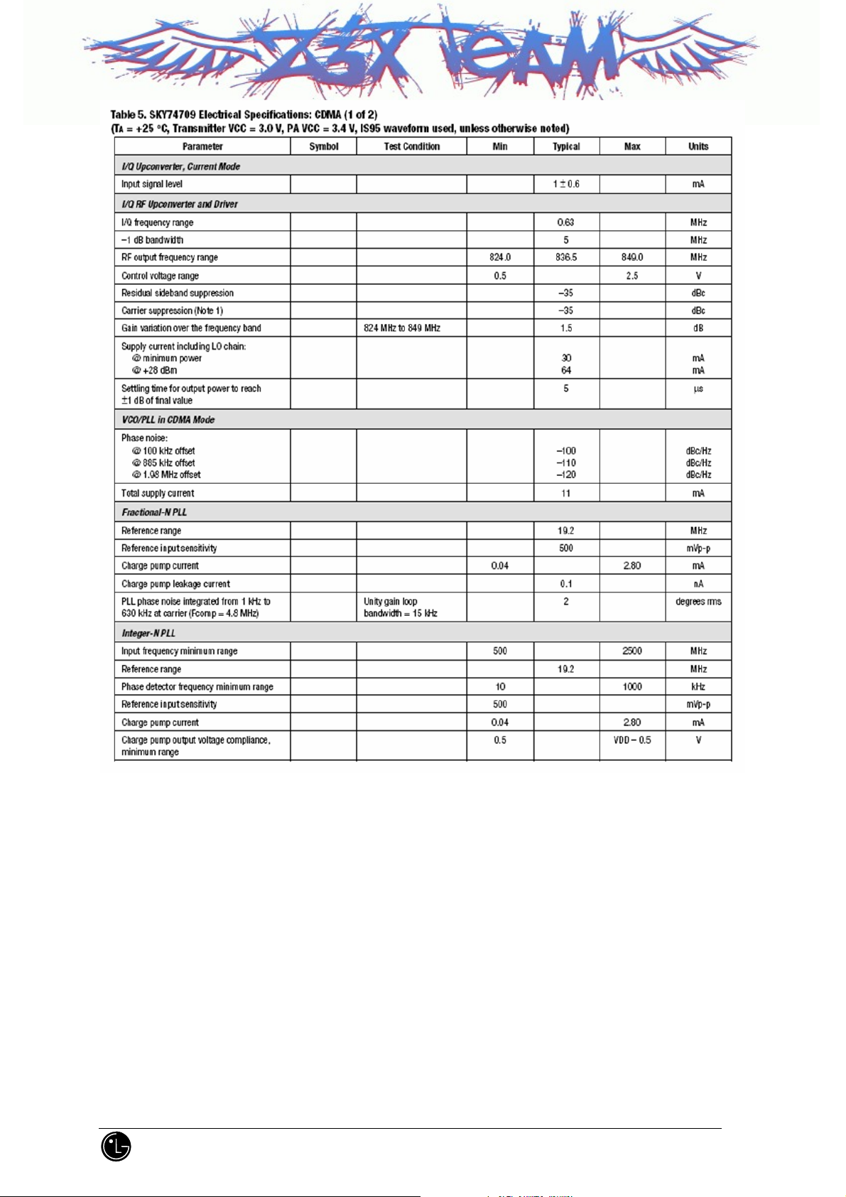
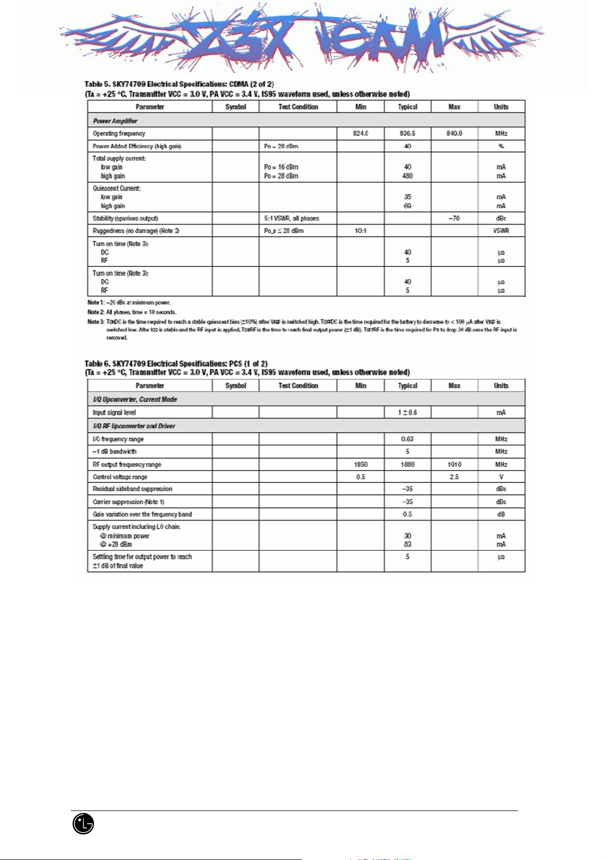
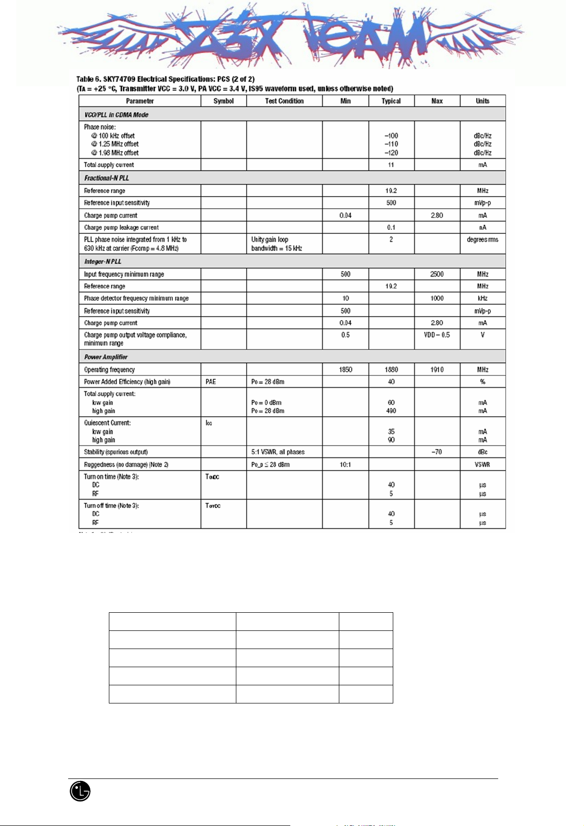
1. Specification
1.1 General Specification
1.1.1 Transmit/Receive Frequency Interval
1) CELLULAR : 70MHz
2) PCS : 140 MHz
1.1.2 Number of Channels (Channel Bandwidth)
1) CELLULAR : 20 Channels
2) PCS : 48 Channels
1.1.3 Operating Voltage : DC 3.2~4.1V
1.1.4 Battery Power Consumption : DC 3.7V
SLEEP IDLE MAX POWER
CELLULAR
PCS
1.1.5 Operating Temperature : -30°C ~ +60°C
1.1.6 Frequency Stability
1) CDMA : ±0.5PPM
2) PCS : ±0.1PPM
1.1.7 Antenna : Fixed Type, 50 Ω
1.1.8 Size and Weight
1) Size : 97.8(H) * 48(W) * 15.2(D) mm
2) Weight : 110 g (Approximately with standard battery)
1.1.9 Channel Spacing
1) CELLULAR : 1.25MHz
2) PCS : 1.25 MHz
1.5 mA 110 ~ 120mA 700 mA (24 dBm)
1.5 mA 120 ~ 130 mA 700 mA (24 dBm)
Z3X-BOX.COM
LG Electronics Inc.

1.1.10 Battery Type, Capacity and Operating Time.
Unit = Hours : Minutes
Standard (800mAh)
CELLULAR
Standby Time
PCS
CELLULAR
Talk time
PCS
1.2 Receive Specification
1.2.1 Frequency Range
1) CELLULAR : 869 MHz ~ 894 MHz
2) PCS : 1930 MHz ~ 1990 MHz
3) GPS : 1575.42 MHz
1.2.2 Local Oscillating Frequency Range :
1) CELLULAR : 3476 MHz ~ 3576 MHz
2) PCS : 3860 MHz ∼ 3980 MHz
3) GPS : 3150.84 MHz
160 Hrs (Slotted mode 2, sector
pwr :-75dBm)
160 Hrs (Slotted mode 2, sector
pwr :-75dBm)
144 minute (Rx Power -92dBm, Half rate)
144 minute (Rx Power -92dBm, Half rate)
1.2.3 Sensitivity
1) CELLULAR : -104 dBm (C/N 12dB or more)
2) PCS : -104 dBm (C/N 12dB or more)
3) GPS : -148.5 dBm (w/o SA), -152 dBm (w/SA)
1.2.4 Selectivity
1) CELLULAR : 3dB C/N Degration (With Fch±1.25 KHz : -30dBm)
2) PCS : 3dB C/N Degration (With Fch±1.25 KHz : -30dBm)
1.2.5 Interference Rejection
1) Single Tone : -30dBm at 900 kHz (CELLULAR), -30dBm at 1.25MHz(PCS)
2) Two Tone : -43dBm at 900 kHz & 1700kHz(CELLULAR), -43dBm at 1.25 MHz & 2.05 MHz
1.2.6 Spurious Wave Suppression : Maximum of -80dB
1.2.7 CDMA Input Signal Range
Dynamic area of more than -104~ -25 dB: 79dB at the 1.23MHz band.
z
Transmit Band : below –60dBm
z
Z3X-BOX.COM
LG Electronics Inc.

Receive Band : below –80dBm
z
1.3 Transmit Specification
1.3.1 Frequency Range
1) CELLULAR : 824MHz ~ 849MHz
2) PCS : 1850 MHz ~ 1910 MHz
1.3.2 Output Power
1) CELLULAR : 0.224 W
2) PCS: 0.224 W
1.3.3 CDMA TX Frequency Deviation :
1) CELLULAR: +300Hz or less
2) PCS: ± 150Hz
1.3.4 CDMA TX Conducted Spurious Emissions
1) CELLULAR : 900kHz : - 42 dBc/30kHz below
1.98MHz : - 54 dBc/30kHz below
2) PCS : -42 dBc / 30KHz below
1.3.5 CDMA Minimum TX Power Control
1) CELLULAR : - 50dBm below
2) PCS: -50dBm below
1.4 MS (Mobile Station) Transmitter Frequency
1.4.1 CELLULAR mode
Ch # Center Freq. (MHz) Ch # Center Freq. (MHz)
Z3X-BOX.COM
LG Electronics Inc.
1011
824.640
404
837.120
29
70
111
152
193
234
275
316
363
825.870
827.100
828.330
829.560
830.790
832.020
833.250
834.480
835.890
445
486
527
568
609
650
697
738
779
838.350
839.580
840.810
842.040
843.270
844.500
845.910
847.140
848.370
1.4.2 PCS mode
Ch # Center Freq (MHz) Ch # Center Freq (MHz) Ch # Center Freq (MHz)
25 1851.25 425 1871.25 825 1891.25
50 1852.50 450 1872.50 850 1892.50
75 1853.75 475 1873.75 875 1893.75
100 1855.00 500 1875.00 900 1895.00
125 1856.25 525 1876.25 925 1896.25
150 1857.50 550 1877.50 950 1897.50
175 1858.75 575 1878.75 975 1898.75
200 1860.00 600 1880.00 1000 1900.00
225 1861.25 625 1881.25 1025 1901.25
250 1862.50 650 1882.50 1050 1902.50
275 1863.75 675 1883.75 1075 1903.75
300 1865.00 700 1885.00 1100 1905.00
325 1866.25 725 1886.25 1125 1906.25
350 1867.50 750 1887.50 1150 1907.50
375 1868.75 775 1888.75 1175 1908.75
Z3X-BOX.COM
1.5
MS (Mobile Station) Receiver Frequency
1.5.1 CELLULAR mode
Ch. # Center Freq. (MHz) Ch. # Center Freq. (MHz)
1011
29
70
111
LG Electronics Inc.
869.640
870.870
872.100
873.330
404
445
486
527
882.120
883.350
884.580
885.810
152
874.560
568
887.040
193
234
275
316
363
1.5.2 PCS mode
Ch # Center Freq (MHz) Ch # Center Freq (MHz) Ch # Center Freq (MHz)
25 1931.25 425 1951.25 825 1971.25
50 1932.50 450 1952.50 850 1972.50
75 1933.75 475 1953.75 875 1973.75
100 1935.00 500 1955.00 900 1975.00
125 1936.25 525 1956.25 925 1976.25
875.790
877.020
878.250
879.480
880.890
609
650
697
738
779
888.270
889.500
890.910
892.140
893.370
150 1937.50 550 1957.50 950 1977.50
175 1938.75 575 1958.75 975 1978.75
200 1940.00 600 1960.00 1000 1980.00
225 1941.25 625 1961.25 1025 1981.25
250 1942.50 650 1962.50 1050 1982.50
275 1943.75 675 1963.75 1075 1983.75
300 1945.00 700 1965.00 1100 1985.00
325 1946.25 725 1966.25 1125 1986.25
350 1947.50 750 1967.50 1150 1987.50
375 1948.75 775 1968.75 1175 1988.75
1.5.3 GPS mode
- Center Freq. : 1575.42MHz
Z3X-BOX.COM
1.6 AC Adapter : See Appendix
1.7 Cigarret Lighter Adapter : See Appendix
LG Electronics Inc.

1.8 Portable Hands-Free Kit : See Appendix
Z3X-BOX.COM
LG Electronics Inc.

2. Installation
2.1 Installing a Battery Pack
1) The Battery pack is keyed so it can only fit one way. Align the groove in the battery pack with the rail on the
back of the phone until the battery pack rests flush with the back of the phone.
2) Slide the battery pack forward until you hear a “click”, which locks the battery in place.
2.2 For Adapter Use
1) Plug the adapter into a wall outlet. The adapter can be operated from a 110V source. When AC power is
connected to the adapter.
2) Insert the adapter jack into the phone with the installed battery pack.
2.3 For Mobile Mount
2.3.1 Installation Position
In order to reduce echo sound when using the Hands-Free Kit, make sure that the speaker and microphone are
not facing each other and keep microphone a generous distance from the speaker.
2.3.2 Interface Box
Choose an appropriate flat surface ( somewhere under the dash on the passenger side is preferred ) and mount
the IB bracket with the four self-tapping screws provided. Clip the IB into the IB bracket.
2.3.3. Microphone Installation
Install the microphone either by clipping I onto the sunvisor (driver’s side) or by attaching it to door post
(driver’s side), using a velcno adhesive tape (not included).
2.3.4 Cable Connections
2.3.5
Power and Ignition Cables
Z3X-BOX.COM
LG Electronics Inc.
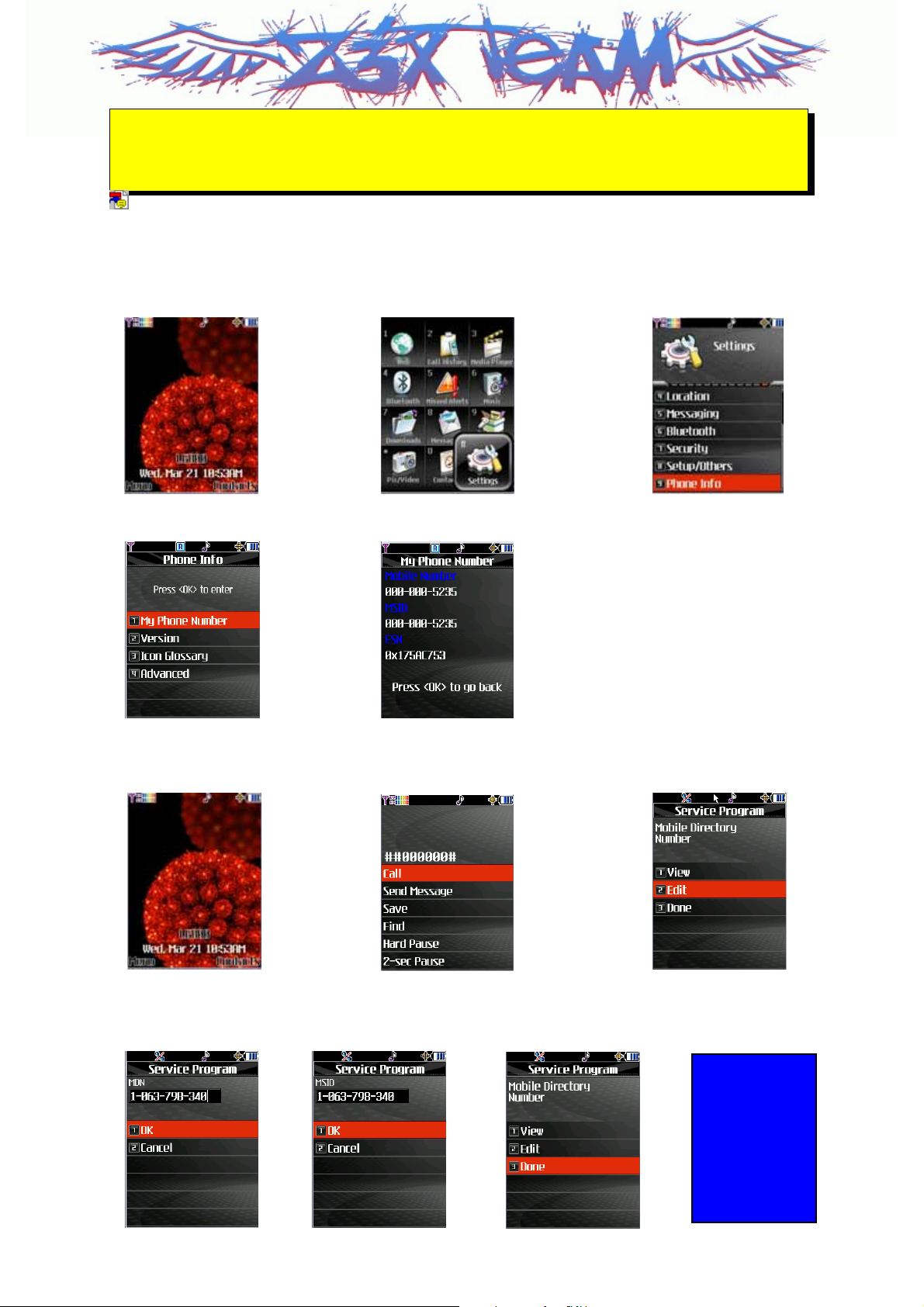
CHAPTER 2. NAM Input Method
(Inputting of telephone numbers included)
1. NAM Program Method and Telephone Number Inputting Method
1. 1 Check ESN (Read only)
Idle Screen Enter ‘MENU’, And Press “#” Press “9”
Î Î
Press “1” You can see ESN and PHONE NUMBER.
Î
1.2 Write PHONE NUMBER.
Idle Screen Press “##000000#” Press “2”
Î Î
Z3X-BOX.COM
Enter PHONE NUMBER(MDN) Enter PHONE NUMBER(MSID)
And Press “OK”. And Press “OK” Press “3” Phone is reset.
Î Î Î
Powering Off

CHAPTER 3. Circuit Description
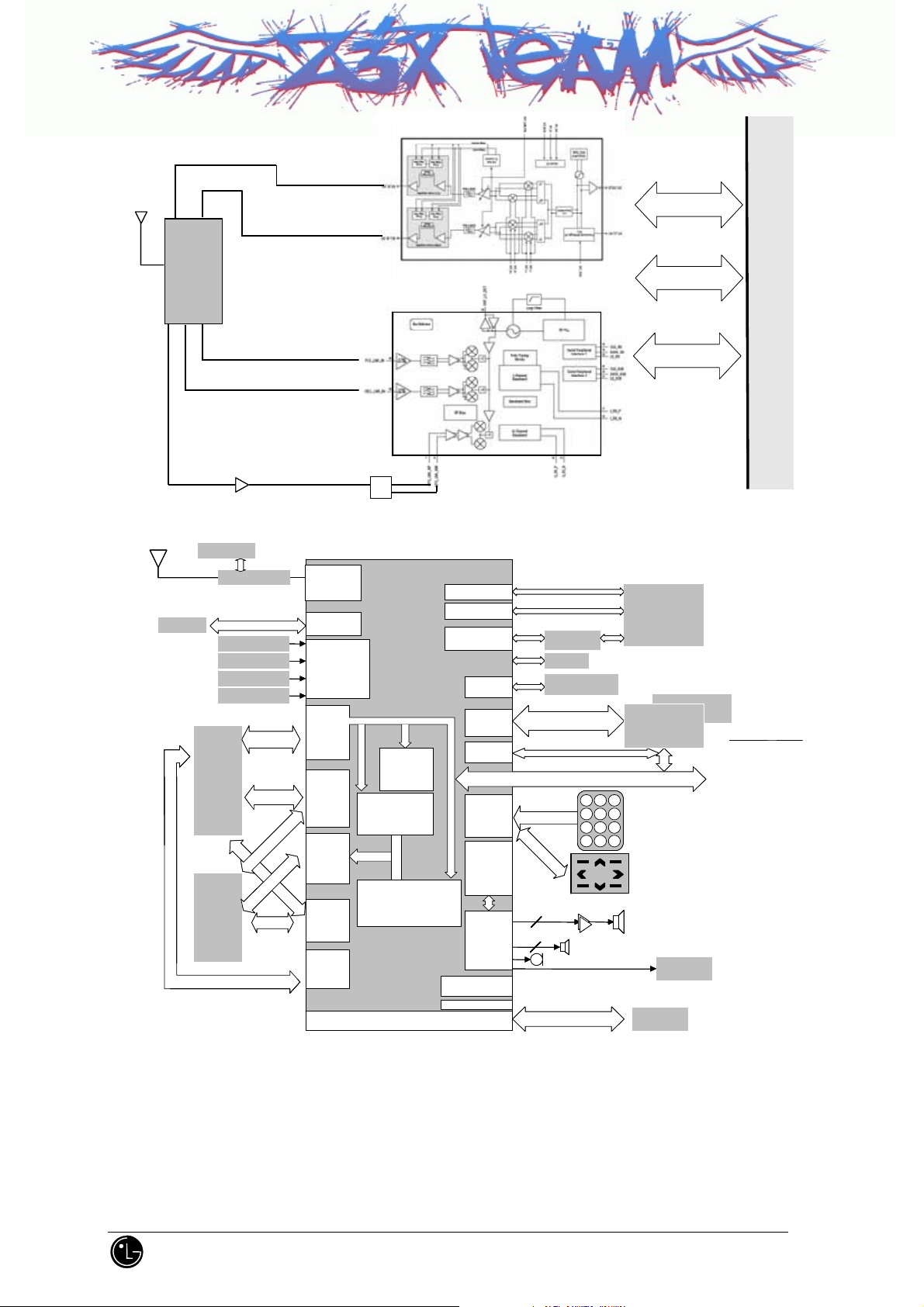
1. RF Transmit/Receive Part
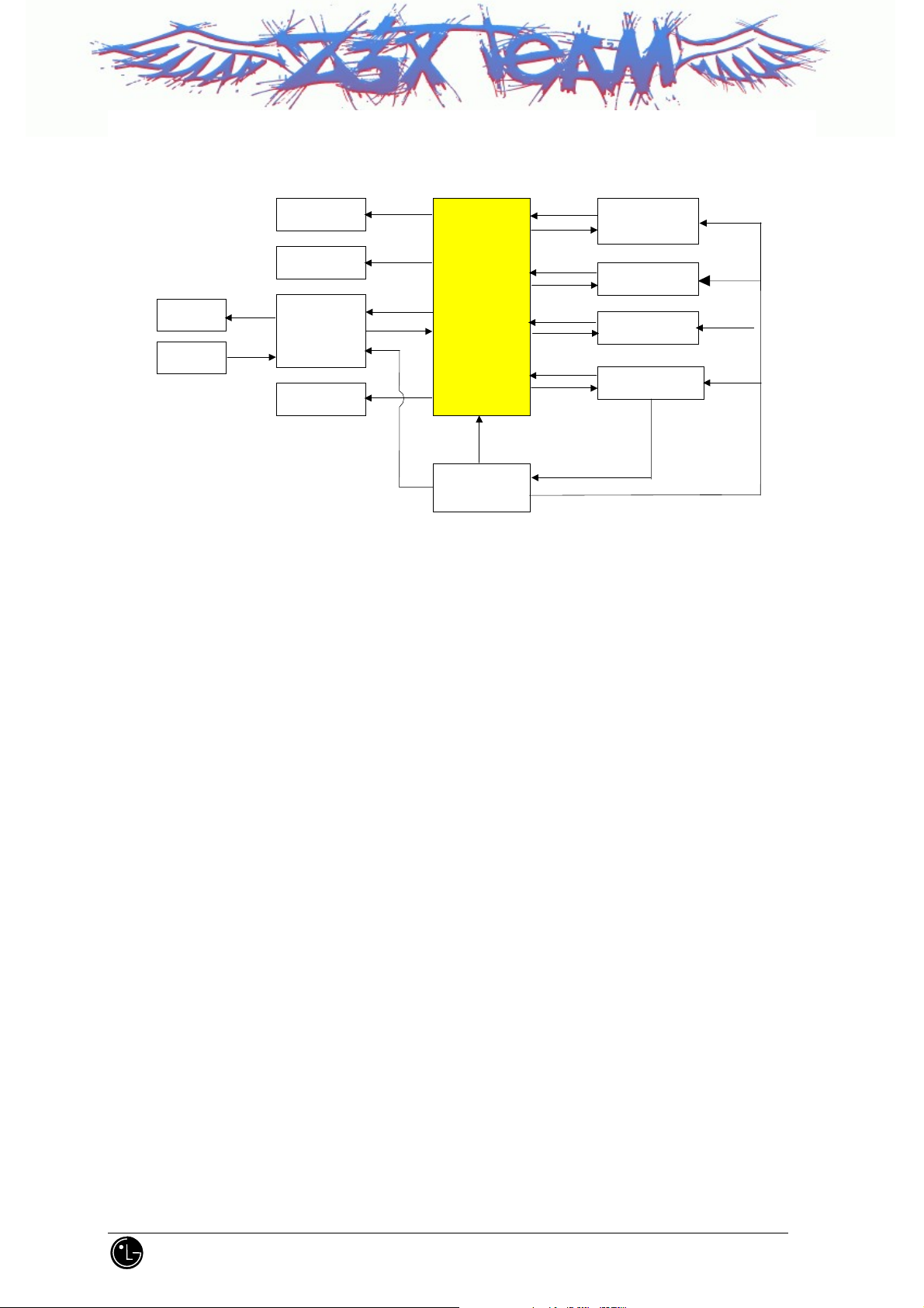
1.1 Overview
The Tx and Rx part employs the Direct-Conversion system. The Tx and Rx frequencies are respectively
824.04~848.97 and 869.04~893.97 for cellular and 1850~1910 and 1930~1990 for PCS. The block diagram is
shown in [Figure 1-1]. RF signals received through the antenna are seperated by the Quintplexer.
RF Signal fed into Skyworks RX MCM(SKY 74609) through the Quintplexer. In RX MCM, the IF signal is
changed into baseband signal directly. Then, this signal is changed into digital signal by the analog to digital
converter (ADC, A/D Converter), and the digital circuit part of the MSM(Mobile Station Modem) 6500
processes the data from ADC. The digital processing part is a demodulator.
In the case of transmission, TX MCM(SKY 74709) receives OQPSK-modulated anlaog signal from the
MSM6500. The TX MCM connects directly with MSM6500 using an analog baseband interface. In TX MCM,
the baseband quadrature signals are upconverted to the Cellular or PCS frequency bands and amplified to
provide signal drive capability to the pow er amp.
After that, the RF signal is amplified by the TX MCM in order to have enough power for radiation. Finally,
the RF signal is sent out to the cell site via the antenna after going through the Quintplexer.
Z3X-BOX.COM
LG Electronics Inc.
Antenna
Antenna
B/T Chip
B/T Chip
B/T Chip
Antenna
Antenna
Antenna
Quint-
Quint-
plexer
plexer
GPS
GPS
LNA
LNA
BT_VCTCXO
BT_VCTCXO
BT_VCTCXO
Bluetooth RF
Bluetooth RF
Bluetooth RF
VCTCXO 19.2MHz
VCTCXO 19.2MHz
VCTCXO 19.2MHz
INNER CHG
INNER CHG
INNER CHG
BATTERY
BATTERY
BATTERY
+2.9V_Rx_LDO
+2.9V_Rx_LDO
+2.9V_Rx_LDO
HDET
HDET
HDET
SKY
SKY
SKY
74609
74609
74609
RX
RX
RX
SKY
SKY
SKY
74609
74609
74609
TX
TX
TX
RF Interface
RF Interface
SKY 74709
SKY 74709
SKY 74609
GPS
GPS
BPF
BPF
MSM6500
MSM6500
Bluetooth
Bluetooth
Bluetooth
Baseband
Baseband
Baseband
Processor
Processor
Processor
PLL
PLL
PLL
HK ADC
HK ADC
HK ADC
Rx
Rx
Rx
ADCs
ADCs
ADCs
RF
RF
RF
Interface
Interface
Interface
TX
TX
TX
DACs
DACs
DACs
Z3X-BOX.COM
AUX
AUX
AUX
SBI
SBI
SBI
SBI
SBI
SBI
MSM6500
Mobile Station Modem
Mobile Station Modem
Mobile Station Modem
gpsOne
gpsOne
gpsOne
Processor
Processor
Processor
CDMA
CDMA
CDMA
Processor
Processor
Processor
DFM
DFM
DFM
Processor
Processor
Processor
JTAG Interfaces
JTAG Interfaces
JTAG Interfaces
SKY 74609
UART1
UART1
UART1
UART2
UART2
UART2
UART3/USB
UART3/USB
UART3/USB
CAMIF
CAMIF
CAMIF
ARM9
ARM9
ARM9
TDMI
TDMI
TDMI
Memory
Memory
Memory
Controller
Controller
Controller
General-
General-
GeneralPurpose
Purpose
Purpose
Interface
Interface
Interface
Vocoder
Vocoder
Vocoder
EVRC
EVRC
EVRC
13k
13k
13k
MP4
MP4
MP4
MIDI
MIDI
MIDI
QDSP4000
QDSP4000
QDSP4000
Integrated
Integrated
Integrated
CODEC
CODEC
CODEC
MODE Select
MODE Select
MODE Select
Interface
Interface
Interface
ETM
ETM
ETM
Data Comm
Data Comm
Data Comm
DM
DM
DM
USB
USB
USB
USB
USB
USB
Transceiver
Transceiver
Transceiver
LDO
LDO
LDO
Camera module
Camera module
Camera module
(1.3M C-MOS)
(1.3M C-MOS)
(1.3M C-MOS)
Microprocessor Bus
Microprocessor Bus
Microprocessor Bus
Address/Data
Address/Data
Address/Data
General-Purpose Interface Bus
General-Purpose Interface Bus
General-Purpose Interface Bus
1 2 3
1 2 3
1 2 3
4 5 6
4 5 6
Keypad input
Keypad input
Keypad input
2
2
2
2
2
2
4 5 6
7 8 9
7 8 9
7 8 9
* #0
* #0
* #0
OK
OK
OKOK
Audio AMP
Audio AMP
Audio AMP
EAR
EAR
EAR
MIC
MIC
MIC
Digital Test Bus JTAG
Digital Test Bus JTAG
Digital Test Bus JTAG
TX,RX I Q
TX,RX I Q
SBI,AUX SBI
SBI,AUX SBI
PC
PC
PC
Connectivity
Connectivity
Connectivity
Test/Debug
Test/Debug
Test/Debug
System
System
System
Memory
Memory
Memory
NAND Flash(2Gb)
NAND Flash(2Gb)
NAND Flash(2Gb)
LP-SDRAM(512Mb)
LP-SDRAM(512Mb)
LP-SDRAM(512Mb)
KEYPAD, BEZEL ,
KEYPAD, BEZEL ,
KEYPAD, BEZEL ,
SIIDEKEY
SIIDEKEY
SIIDEKEY
Touch Key PAD
Touch Key PAD
Touch Key PAD
Speaker
Speaker
Speaker
External
External
External
EAR/MIC
EAR/MIC
EAR/MIC
LCD
LCD
LCD
MSM
MSM
6500
6500
Peripheral Circuits
Peripheral Circuits
Peripheral Circuits
[Figure 1-1] Block Diagram Of CX800
1.2 Description of Receive Part Circuit
LG Electronics Inc.

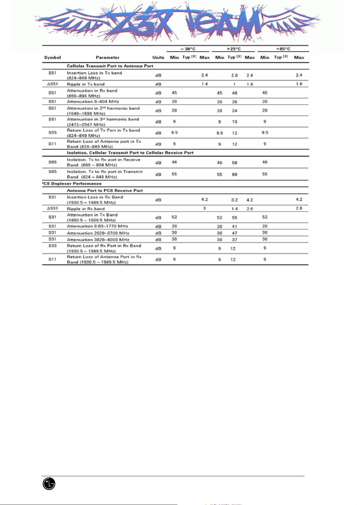
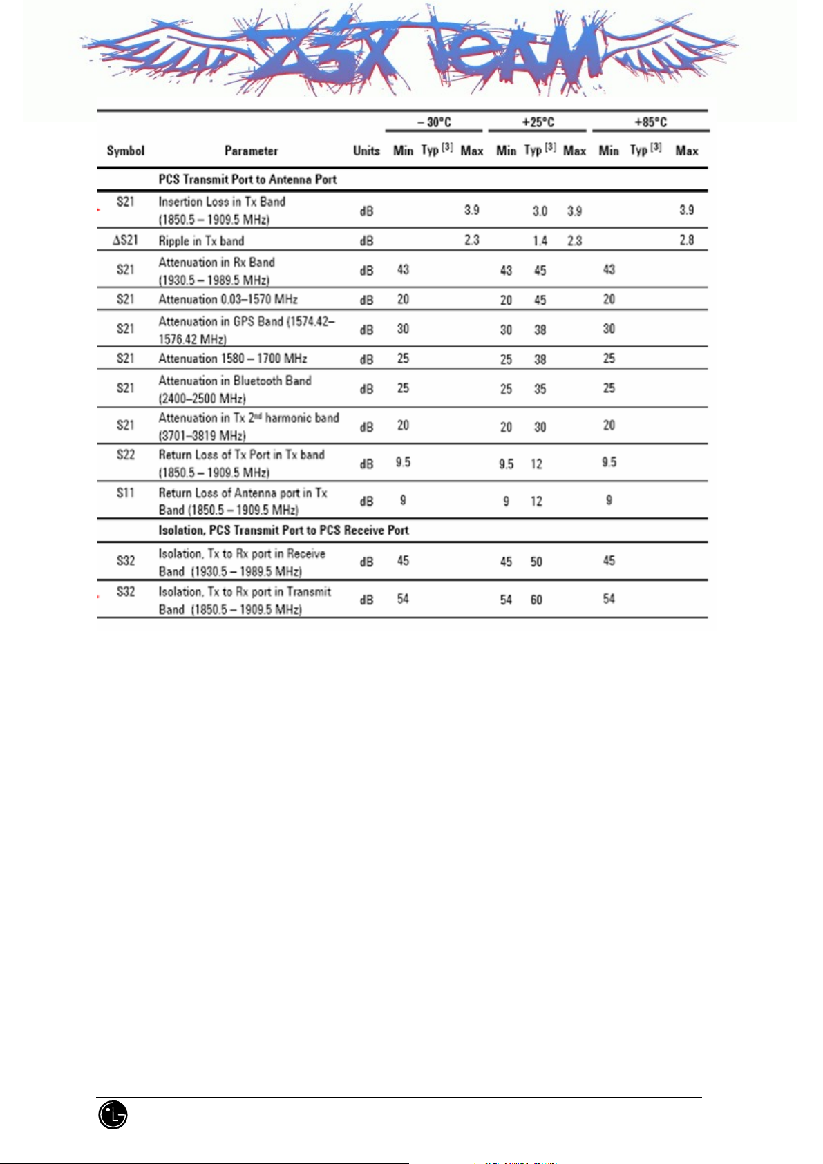
1.2.1 Quintplexer (U105)
The ACFM-7101 is a Quintplexer that combines a US PCS duplexer, a cellular band duplexer and a GPS
band filter into a single, miniature package with a single antenna port
The main function of Quintplexer(ACFM-7101) is to prohibit the other band signals from flowing into the
one band circuit and vice versa. RF designer can use common tri-band antenna regardless of frequency band
(800, 1575 and 1900 MHz). The specification of CX800 Quintplexer is described below:
.
Z3X-BOX.COM
LG Electronics Inc.
Z3X-BOX.COM
LG Electronics Inc.
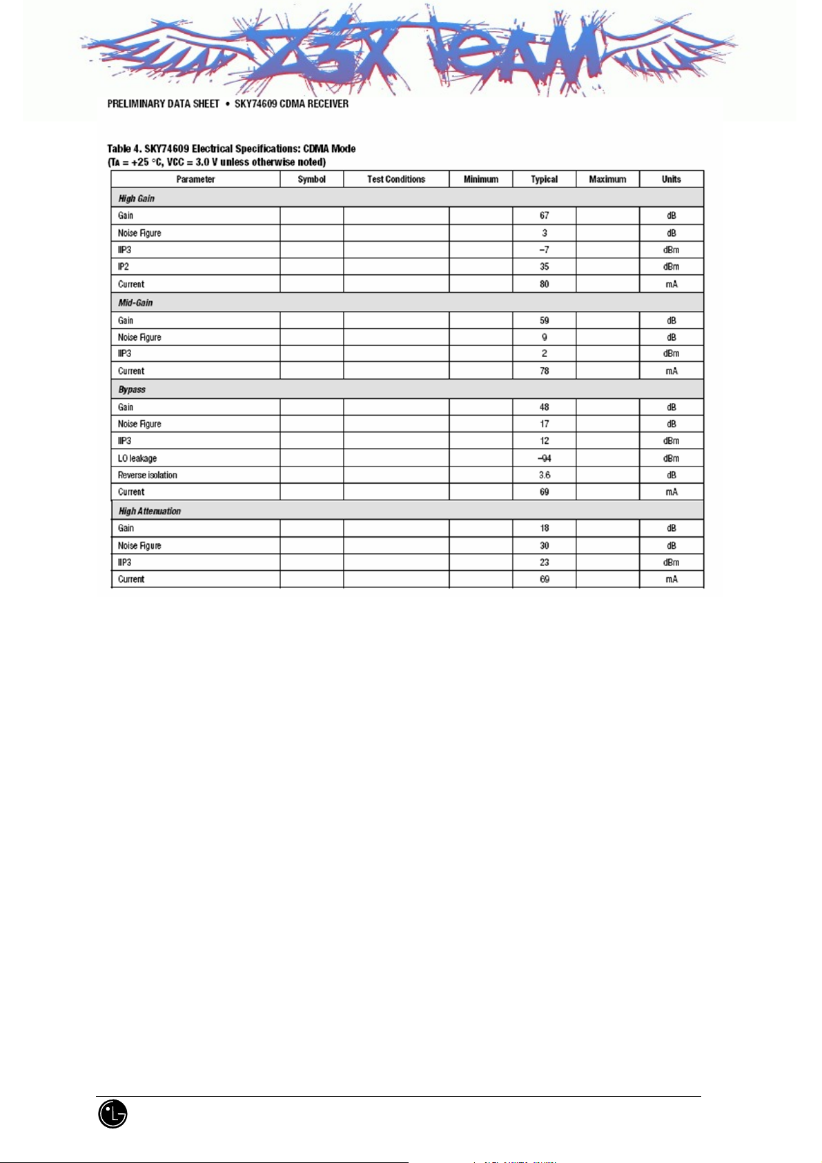
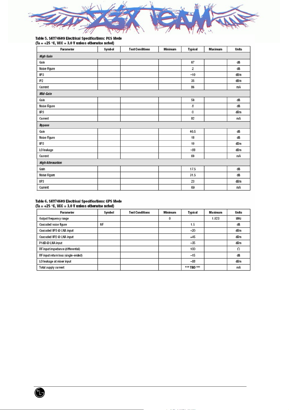
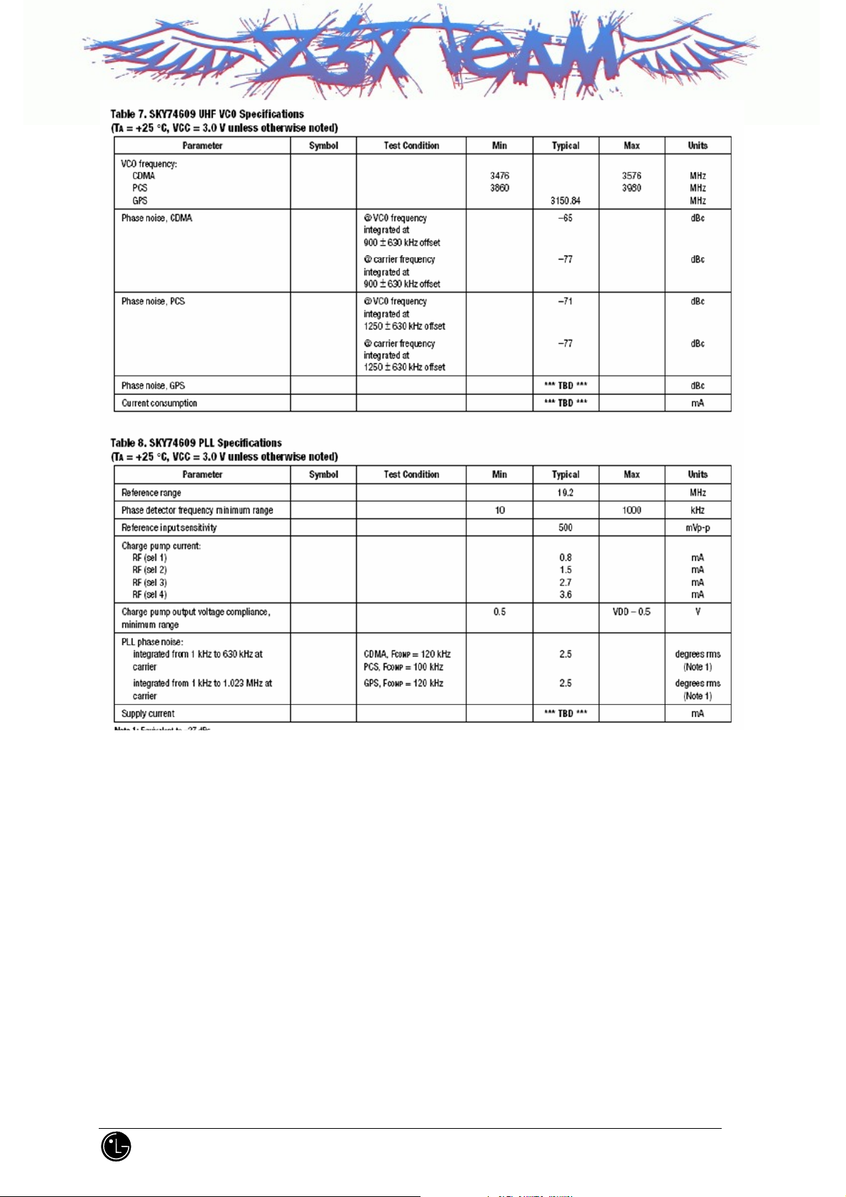
1.2.2
The SKY74609 receiver is a highly integrated device for tri-band, dual-mode Code Division Multiple Access
(CDMA) handsets with Global Positioning System (GPS) capability. The SKY74609 supports CDMA phones in
the cellular CDMA, Personal Communications System (PCS), and GPS modes. The device requires a minimum
number of external components to complete a CDMA radio subsystem. Included on-chip are the down converter,
base band filters with auto-tuning loop, UHF Voltage Controlled Oscillator (VCO), RF Phase Locked
Loop(PLL),and DC Offset Compensation (DCOC).External components needed for operation include matching
networks for differential mixer inputs and differential GPS Low Noise Amplifier (LNA) inputs, CDMA/PCS
Surface Acoustic Wave (SAW) filters, three bias resistors for accurate bias control over process variation, and
two high tolerance load resistors for In- Phase and Quadrature (I/Q) baseband output. The SKY74609 output is a
dual-channel, fully differential analog signal at the baseband. Both channels maintain a quadrature phase
relationship with each other.
RX MCM (SKY74609: U104)
Z3X-BOX.COM
LG Electronics Inc.
Z3X-BOX.COM
LG Electronics Inc.
Z3X-BOX.COM
LG Electronics Inc.
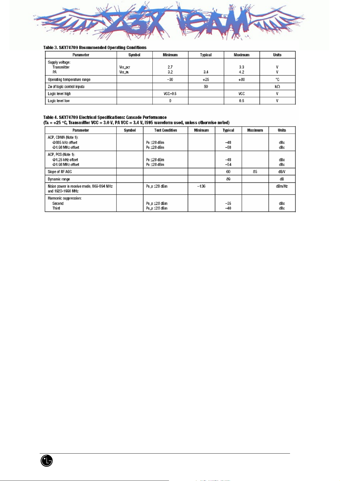
1.2.3 TX MCM (SKY74709: U103)
The SKY74709 transmitter is a highly integrated device designed for dual-band, single-mode CDMA handsets
in the cellular CDMA and Personal Communications System (PCS) modes. The SKY74709 includes interstage
transmit Surface Acoustic Wave (SAW) filters and separate CDMA and PCS Gallium Arsenide
(GaAs) Microwave Monolithic Integrated Circuit (MMIC) Power Amplifiers (PAs). The device meets the
stringent CDMA linearity requirements up to 28 dBm output power. The incoming CDMA baseband signal is
upconverted to the desired RF frequency by the In-Phase and Quadrature (I/Q) modulator and amplified by the
appropriate PA driver stage to provide variable outpu t p ower. The signal is filtered by an interstage transmit
SAW filter and sent to the respective PA to obtain the final rated power.
The only external components needed to complete a CDMA radio subsystem are supply bypass capacitors and
filtering capacitors at the I/Q inputs. The required Phase Lock Loop (PLL) filter and bias resistors have been
included on-chip. The state of the PAs is controlled by the SKY74709, which eliminates the need for
external switches to enable/disable the PAs and control their gain. The SKY74709 is designed to operate within
a supply voltage range of 3.2 V to 4.2 V. Together with the SKY74609 receiver, the SKY74709 transmitter
forms Skyworks Tri-Band, Dual-Mode CDMA RF Subsystem. This subsystem is compliant with the IS-95,
CDMA2000, and E-911standards.
Z3X-BOX.COM
LG Electronics Inc.
Z3X-BOX.COM
LG Electronics Inc.
Z3X-BOX.COM
LG Electronics Inc.
Z3X-BOX.COM
LG Electronics Inc.
1.2.4 GPS LAN(U102)
The characteristics of Low Noise Amplifier (LNA) are low noise figure, high gain, high intercept point and
high reverse isolation. The frequency selectivity characteristic of mobile phone is mostly determined by LNA.
The specification of CX800 GPS LNA is described below
Z3X-BOX.COM
Parameter GPS Band Units
Gain
Noise Figure
1dB compression point
IIP3
LG Electronics Inc.
17.7 dB
0.6 dB
14.4 dBm
6.5 dBm

1.2.5 GPS Rx RF SAW FILTER(F100)
The main function of GPS Rx RF SAW filter is to attenuate mobile phone spurious frequency, attenuate noise
amplified by the GPS LNA and suppress second harmonic originating in the GPS LNA.
1.3 Description of Frequency Synthesizer Circuit
1.3.1 Voltage Control Temperature Compensation Crystal Oscillator (VCTCXO, F101)
The temperature variation of mobile phone can be compensated by VCTCXO. The reference frequency of a
mobile phone is 19.2 MHz. The receiver frequency tuning signals called TRK_LO_ADJ from MSM as 0.5
V~2.5 V DC via R and C filter in order to generate the reference frequency of 19.2 MHz and input it into the
frequency synthesizer. Frequency stability depending on temperature is ±2.0 ppm.
Z3X-BOX.COM
LG Electronics Inc.

2. Digital/Voice Processing Part
2.1 Overview
The digital/voice processing part processes the user's commands and processes all the digital and voice signal
processing in order to operate in the phone. The digital/voice processing part is made up of a keypad/LCD,
receptacle part, voice processing part, mobile station modem part, memory part, and power supply part.
2.2 Configuration
2.2.1 Keypad/LCD and Receptacle Part
This is used to transmit keypad signals to MSM6500. It is made up of a keypad backlight part that illuminates
the keypad, LCD part that displays the operation status onto the screen, and a receptacle that receives and sends
out voice and data with external sources.
2.2.2 Voice Processing Part
The voice processing part is made up of an audio codec used to convert MIC signals into digital voice signals
and digital voice signals into analog voice signals, amplifying part for amplifying the voice signals and sending
them to the ear piece, amplifying part that amplifies ringer signals coming out from MSM6500, and amplifying
part that amplifies signals coming out from MIC and transferring them to the audio processor.
2.2.3 MSM (Mobile Station Modem) 6500 Part
MSM is the core elements of CDMA terminal and carries out the functions of CPU, encoder, interleaver,
deinterleaver, Viterbi decoder, Mod/Demod, and vocoder.
2.2.4 Memory Part
The memory part is made up of a flash memory, SRAM for storing data. Our memory is consist of 2G NAND
flahs memory and 512 SRAM.
2.2.5 Power Supply Part
The power supply part is made up of circuits for generating various types of power, used for the digital/voice
processing part.
Z3X-BOX.COM
LG Electronics Inc.

2.3 Circuit Description
2.3.1 Keypad/LCD and Receptacle Part
Once the keypad is pressed, the key signals are sent out to MSM6500 for processing. In addition, when the
key is pressed, the keypad lights up through the use of EL. The terminal status and operation are displayed on
the screen for the user with the characters and icons on the LCD.
Moreover, it exchanges audio signals and data with external sources through the receptacle, and then receives
power from the battery or external batteries.
2.3.2 Audio Processing Part
MIC signals are amplified through OP AMP, inputted into the audio codec(included in MSM6500) and
converted into digital signals. Oppositely, digital audio signals are converted into analog signals after going
through the audio codec. These signals are amplified at the audio amplifier and transmitted to the ear-piece. The
signals from MSM6500 activate the ringer by using signals generated in the timer in MSM6500.
2.3.3 MSM Part
MSM6500 is the core element of CDMA system terminal that includes ARM926EJ-S microprocessor core. It
supports both CDMA and Digital FM, operating in both the cellular and PCS spectrums. The subsystems within
the MSM6500 include a CDMA processor, a DFM processor, a multi-standard Vocoder, an integrated CODEC
with earpiece and microphone amplifiers, general-purpose ADC for subsystem monitoring, an ARM926EJ-S
microprocessor, and both Universal Serial Bus(USB) and an RS-232 serial interfaces supporting forward and
reverse link data communications of 307.2 Kbps simultaneously. And it also contains complete digital
modulation and demodulation systems for CDMA standards, as specified in IS-95-A/B/C. In MSM, coded
symbols are interleaved in order to cope with multi-path fading. Each data channel is scrambled by the long
code PN sequence of the user in order to ensure the con fidentiality of calls. Moreover, binary quadr ature codes
are used based on walsh functions in order to discern each channel. Data created thus are 4-phase modulated by
one pair of Pilot PN code and they are used to create I and Q data. When received, I and Q data are
demodulated into symbols by the demodulator, and then de-interleaved in reverse to the case of transmission.
Then, the errors of data received from viterbi decoder are detected and corrected. They are voice-decoded at the
vocoder in order to output digital voice data.
Z3X-BOX.COM
LG Electronics Inc.
LCD
Flash
Memory
Earpiece
Mic
Keypad
MSM6500
Processor
Audio
Ringer
Power
Supply
[Figure 2-2] Block Diagram of Digital/Voice Processing Part
SRAM
CAMERA MODULE
Receptacle
2.3.4 Memory Part
MCP contents 2 Gbits flash memory and 512 Mbits Static RAM. In the Flash Memory part of MCP are
programs used for terminal operation. The programs can be changed through down loading after the assembling
of terminals. On the SRAM data generated during the terminal operation are stored temporarily.
2.3.5 Power Supply Part
When the battery voltage (+3.7V) is fed and the PWR key of keypad is pressed, the power-up circuitry in
Power on & off part is activated by the PWR_ON_SW signal, and then the LDO regulators for MSM are
operated and +1.4V_MSMC, +1.85V_MSMP1,+2.6V_MSMP2, and +2.6V_MSMA are generated.
The Rx part regulator (+2.85V_RX) is operated by the control signal of SLEEP/ from MSM6500
The Tx part regulator (+3.1V_TX) is operated by the control signal of IDLE/ from MSM6500.
The Camera part regulators(+1.5V_CAM_VDD,+2.8V_A_SENSOR,+2.8V_D_SENSOR) are operated by
the control signal of CAMERA_EN/from MSM6500
Z3X-BOX.COM
LG Electronics Inc.

2.3.6 Logic Part
The logic part consists of internal CPU of MSM, RAM(MCP). The MSM6500 receives TCXO (=19.2MHz)
from U104 and controls the phone in both CDMA and FM modes. The major components are as follows:
z
The ARM926EJ-S microprocessor includes a 3 stage pipelined RISC architecture, both 32-bit ARM and
16-bit THUMB instruction sets, a 32-bit address bus, and a 32-bit internal data bus. It has a high performance
and low power consumption.
CPU
z
Flash ROM is used to store the terminal’s program. Using the down-loading program, the program can be
changed even after the terminal is fully assembled.
SRAM is used to store the internal flag information, call processing data, and timer data.
z
For key recognition, key matrix is setup using KYPD[1][3][5][7][9][11][13][15][17][19][21] signal from
MSM. The keypad lights up through the use of EL for easy operation in the dark.
MCP
KEYPAD
LG Electronics Inc.
Z3X-BOX.COM
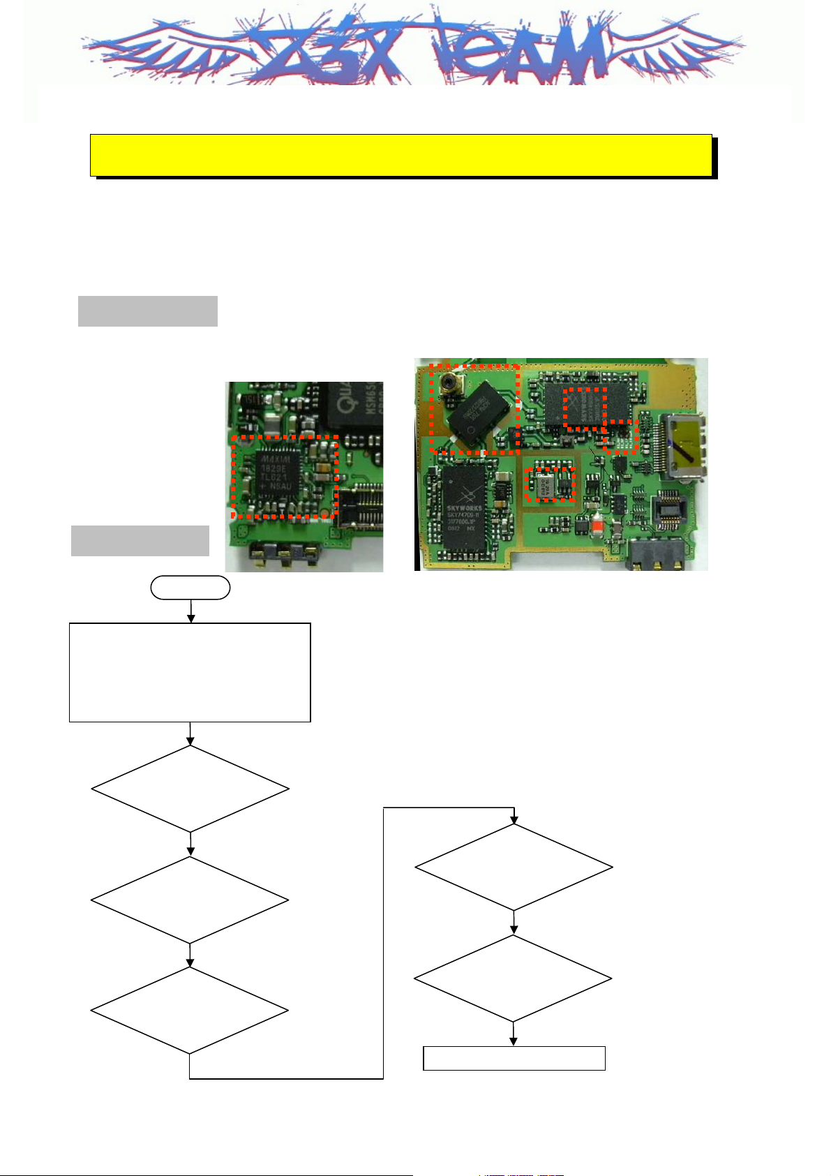
CHAPTER 4. Trouble Shooting
CHAPTER 4. Trouble Shooting
4.1 Rx Part Trouble
4.1.1 When Rx power isn’t enough
Test Point
Figure 4.1-1
CHECK POINTS OF RX PART
1
Checking Flow
START
Rx TEST SETUP(HHP)
- Test Channel : DCN(400) or PCS (600)
E5515C Setup
- CH : DCN(400) or PCS(600)
- Sector Power : -30 dBm
Spectrum Analyzer Setting
Oscilloscope Setting
1. Check
PMIC Circuit
Z3X-BOX.COM
4
3
5
2
2. Check
VCTCXO Circuit
3. Check
Control Signal
4. Check
Duplexer, Mobile SW
5. Check
Rx I/Q data
√ RedownloadSW, CAL
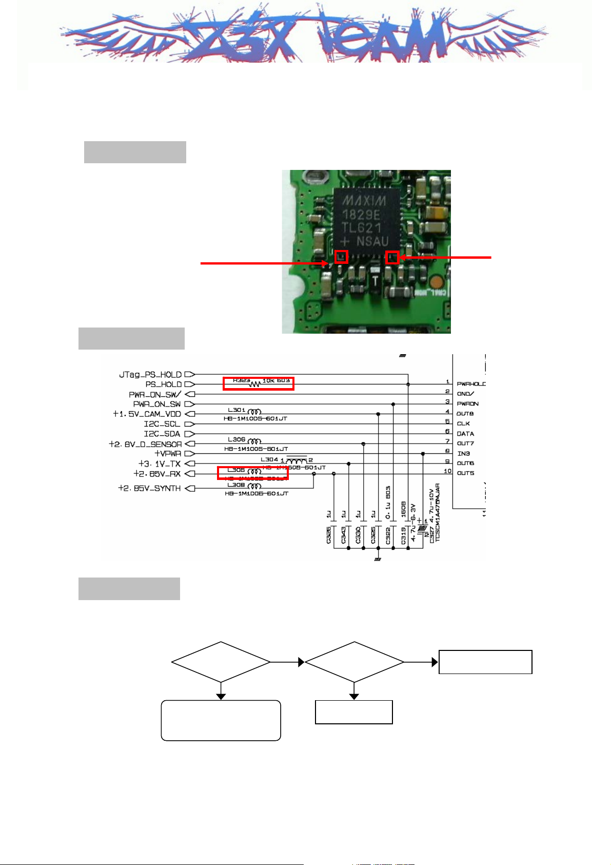
4.1.2 Checking Regulator Circuit
Test Point
U302 Pin 1
PS_Hold
Circuit Diagram
Figure 4.1-3 RX PART CIRCUIT OF MAX1829PMIC
U302 Pin10
+2.85V_RX
Figure 4.1-2
MAX1829 PMIC
Checking Flow
Check Pin 10
of U302
Z3X-BOX.COM
Check Pin 10
of U302
+2.85V_Rx OK?
PMIC Circuit is OK See
next Page to check
VCTCXO
No
Pin 10 High?
YesYes
Replace U302
No
Changing Board
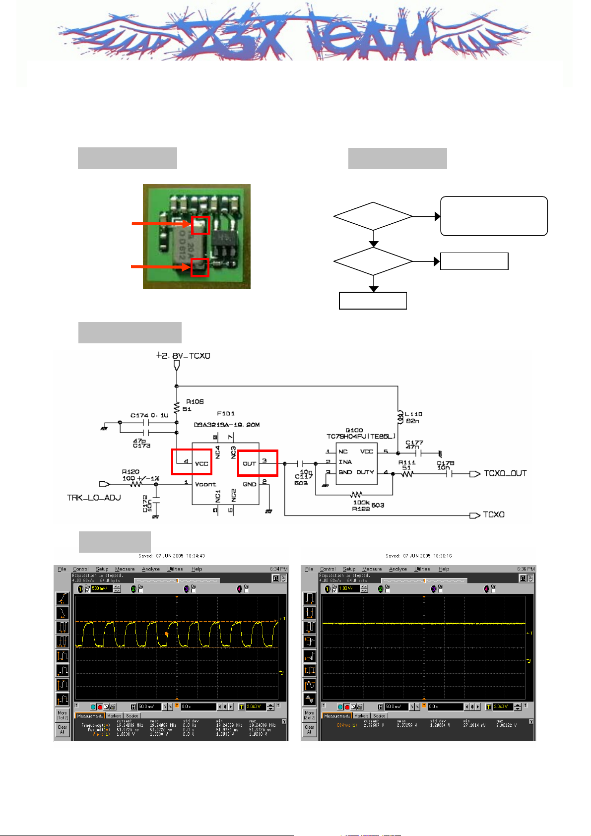
4.1.3 Checking VCTCXO Circuit
Test Point
F101 Pin4
+2.8V_TCXO
F101 Pin3
TCXO
Figure 4.2-6 VCTCXO
Circuit Diagram
Circuit Diagram
Check F101 Pin 3
Check F101 Pin 4
Checking Flow
19.2MHz OK?
No
+2.85V OK?
No
Check U304
Yes
Yes
VCTCXO Circuit is Ok
See next Page to check
Quintplexer
Changing F101
Figure 4.2-7 VCTCXO CIRCUIT
Waveform
Z3X-BOX.COM
Figure 4.1-6 TCXO OUT WAVEFORM Figure 4.1-7 +2.8 5V _TCX O WAV EF ORM
 Loading...