

Page 1

SERVICE MANUAL
SERVICE MANUAL
CAUTION
BEFORE SERVICING THE UNIT, READ THE “SAFETY PRECAUTIONS”
IN THIS MANUAL.
Internal Use Only
MARCH, 2017
MODEL: CJ65 (CJ65, CJS65F)
MODEL: CJ65
(CJ65, CJS65F)
Mini Hi-Fi System
P/NO : AFN77612196
Page 2

CONTENTS
SECTION 1 ........ GENERAL
SECTION 2 ........ CABINET & MAIN CHASSIS
SECTION 3 ........ ELECTRICAL
1-1
Page 3

SECTION 1
SUMMARY
CONTENTS
SERVICING PRECAUTIONS ............................................................................................................................ 1-3
ESD PRECAUTIONS ......................................................................................................................................... 1-5
HIDDEN KEY MODE ......................................................................................................................................... 1-6
1. HIDDEN KEY MODE TABLE .................................................................................................................... 1-6
2. HIDDEN KEY MODE DESCRIPTION ....................................................................................................... 1-7
SERVICE INFORMATION FOR EEPROM ........................................................................................................ 1-9
PROGRAM DOWNLOAD GUIDE .................................................................................................................... 1-10
FOTA UPDATE STEP USING BT APP .......................................................................................................... 1-12
SPECIFICATIONS ........................................................................................................................................... 1-14
1-2
Page 4
1-3
NOTES REGARDING HANDLING OF THE PICK-UP
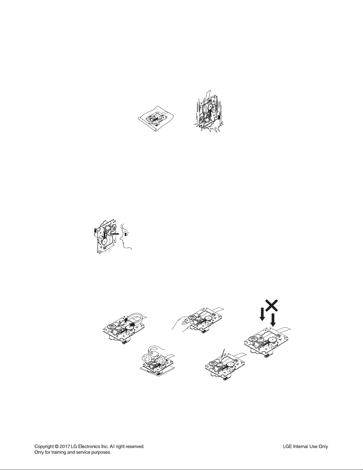
1. Notes for transport and storage
1) The pick-up should always be left in its conductive bag until immediately prior to use.
2) The pick-up should never be subjected to external pressure or impact.
2. Repair notes
1) The pick-up incorporates a strong magnet, and so should never be brought close to magnetic materials.
2) The pick-up should always be handled correctly and carefully, taking care to avoid external pressure and
impact. If it is subjected to strong pressure or impact, the result may be an operational malfunction and/or
damage to the printed-circuit board.
3) Each and every pick-up is already individually adjusted to a high degree of precision, and for that reason
the adjustment point and installation screws should absolutely never be touched.
4) Laser beams may damage the eyes!
Absolutely never permit laser beams to enter the eyes!
Also NEVER switch ON the power to the laser output part (lens, etc.) of the pick-up if it is damaged.
5) Cleaning the lens surface
If there is dust on the lens surface, the dust should be cleaned away by using an air bush (such as used
for camera lens). The lens is held by a delicate spring. When cleaning the lens surface, therefore, a cotton swab should be used, taking care not to distort lens.
6) Never attempt to disassemble the pick-up.
Spring has excess pressure. If the lens is extremely dirty, apply isopropyl alcohol to the cotton swab.
(Do not use any other liquid cleaners, because they will damage the lens.) Take care not to use too much
of this alcohol on the swab, and do not allow the alcohol to get inside the pick-up.
Storage in conductive bag
Drop impact
NEVER look directly at the laser beam, and don’t allow
contact with fingers or other exposed skin.
Magnet
How to hold the pick-up
Conductive Sheet
Cotton swab
Pressure
Pressure
SERVICING PRECAUTIONS
Page 5
NOTES REGARDING COMPACT DISC PLAYER REPAIRS
1. Preparations
1) Compact disc players incorporate a great many ICs as well as the pick-up (laser diode). These components
are sensitive to, and easily affected by, static electricity. If such static electricity is high voltage, components
can be damaged, and for that reason components should be handled with care.
2) The pick-up is composed of many optical components and other high-precision components. Care must be
taken, therefore, to avoid repair or storage where the temperature or humidity is high, where strong magnetism is present, or where there is excessive dust.
2. Notes for repair
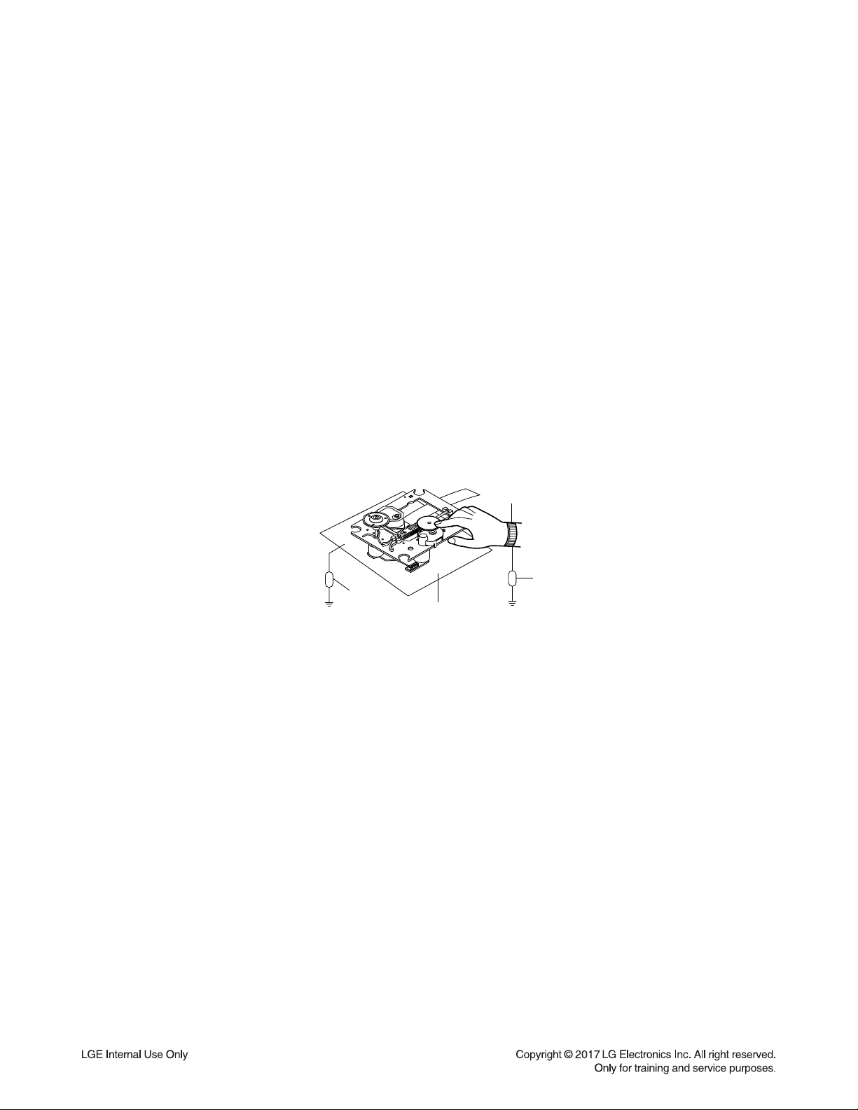
1) Before replacing a component part, first disconnect the power supply lead wire from the unit
2) All equipment, measuring instruments and tools must be grounded.
3) The workbench should be covered with a conductive sheet and grounded.
When removing the laser pick-up from its conductive bag, do not place the pick-up on the bag. (This is
because there is the possibility of damage by static electricity.)
4) To prevent AC leakage, the metal part of the soldering iron should be grounded.
5) Workers should be grounded by an armband (1 M)
6) Care should be taken not to permit the laser pick-up to come in contact with clothing, in order to prevent
static electricity changes in the clothing to escape from the armband.
7) The laser beam from the pick-up should NEVER be directly facing the eyes or bare skin.
Resistor
(1 M)
Conductive
Sheet
Resistor
(1 M)
Armband
1-4
Page 6
1-5
Electrostatically Sensitive Devices (ESD)
Some semiconductor (solid state) devices can be damaged easily by static electricity. Such components
commonly are called Electrostatically Sensitive Devices (ESD). Examples of typical ESD devices are integrated
circuits and some field-effect transistors and semiconductor chip components. The following techniques should
be used to help reduce the incidence of component damage caused by static electricity.
1. Immediately before handling any semiconductor component or semiconductor-equipped assembly, drain off
any electrostatic charge on your body by touching a known earth ground. Alternatively, obtain and wear a
commercially available discharging wrist strap device, which should be removed for potential shock reasons
prior to applying power to the unit under test.
2. After removing an electrical assembly equipped with ESD devices, place the assembly on a conductive surface
such as aluminum foil, to prevent electrostatic charge buildup or exposure of the assembly.
3. Use only a grounded-tip soldering iron to solder or unsolder ESD devices.
4. Use only an anti-static solder removal device. Some solder removal devices not classified as "anti-static" can
generate electrical charges sufficient to damage ESD devices.
5. Do not use freon-propelled chemicals. These can generate electrical charges sufficient to damage ESD
devices.
6. Do not remove a replacement ESD device from its protective package until immediately before you are
ready to install it. (Most replacement ESD devices are packaged with leads electrically shorted together by
conductive foam, aluminum foil or comparable conductive materials).
7. Immediately before removing the protective material from the leads of a replacement ESD device, touch the
protective material to the chassis or circuit assembly into which the device will by installed.
CAUTION : BE SURE NO POWER IS APPLIED TO THE CHASSIS OR CIRCUIT, AND OBSERVE ALL OTHER
SAFETY PRECAUTIONS.
8. Minimize bodily motions when handing unpackaged replacement ESD devices. (Otherwise harmless motion
such as the brushing together of your clothes fabric or the lifting of your foot from a carpeted floor can generate
static electricity sufficient to damage an ESD device).
CAUTION. GRAPHIC SYMBOLS
THE LIGHTNING FLASH WITH APROWHEAD SYMBOL. WITHIN AN EQUILATERAL TRIANGLE, IS
INTENDED TO ALERT THE SERVICE PERSONNEL TO THE PRESENCE OF UNINSULATED
“DANGEROUS VOLTAGE” THAT MAY BE OF SUFFICIENT MAGNITUDE TO CONSTITUTE A RISK OF
ELECTRIC SHOCK.
THE EXCLAMATION POINT WITHIN AN EQUILATERAL TRIANGLE IS INTENDED TO ALERT THE
SERVICE PERSONNEL TO THE PRESENCE OF IMPORTANT SAFETY INFORMATION IN SERVICE
LITERATURE.
ESD PRECAUTIONS
Page 7
1-6
HIDDEN MODE ENTRANCE KEY(Audio) EXIT KEY
Version Check
Front ‘Stop’
+ Remote Control Key ‘Play’ for 5s
Remote Control Key ‘Play’ for 1.5s
EEPROM INITIAL
Front ‘Stop’
+ Remote Control Key ‘ ‘ for 5s
Auto exit
Option EDIT
Front ‘Stop’
+ Remote Control Key ‘ ‘ for 5s
Front ‘Stop’ + Remote Control Key ‘ ‘
APD Test Display
Front ‘Stop’
+ Remote Control Key ‘3’ for 5s
Auto exit
Disc Lock On/Off
Front ‘Stop’ +
Remote Control Key ‘Stop’ for 5s
Front ‘Stop’
+ Remote Control Key ‘Stop’ for 5s
Power Disc Lock On/Off
Front ‘Stop’ + Front ‘Open’ for 5s Front ‘Stop’ + Front ‘Open’ for 5s
Demo ALL Key Lock
Front ‘Stop’
+ Remote Control Key ‘9’ for 5s
Front ‘Stop’
+ Remote Control Key ‘9’ for 5s
BT Auto Power On/Off Front/Remote Control Key ‘Power’ for 5s
Front/Remote Control Key ‘Power’
SET Power Off
ChildSafe On/Off Volume 0(Min) + Front ‘OK’ for 3s Volume 0(Min) + Front ‘OK’ for 3s
Measure
Front ‘Stop’
+ Remote Control Key ‘1’ for 5s
Remote Control Key ‘SOUND EFFECT’
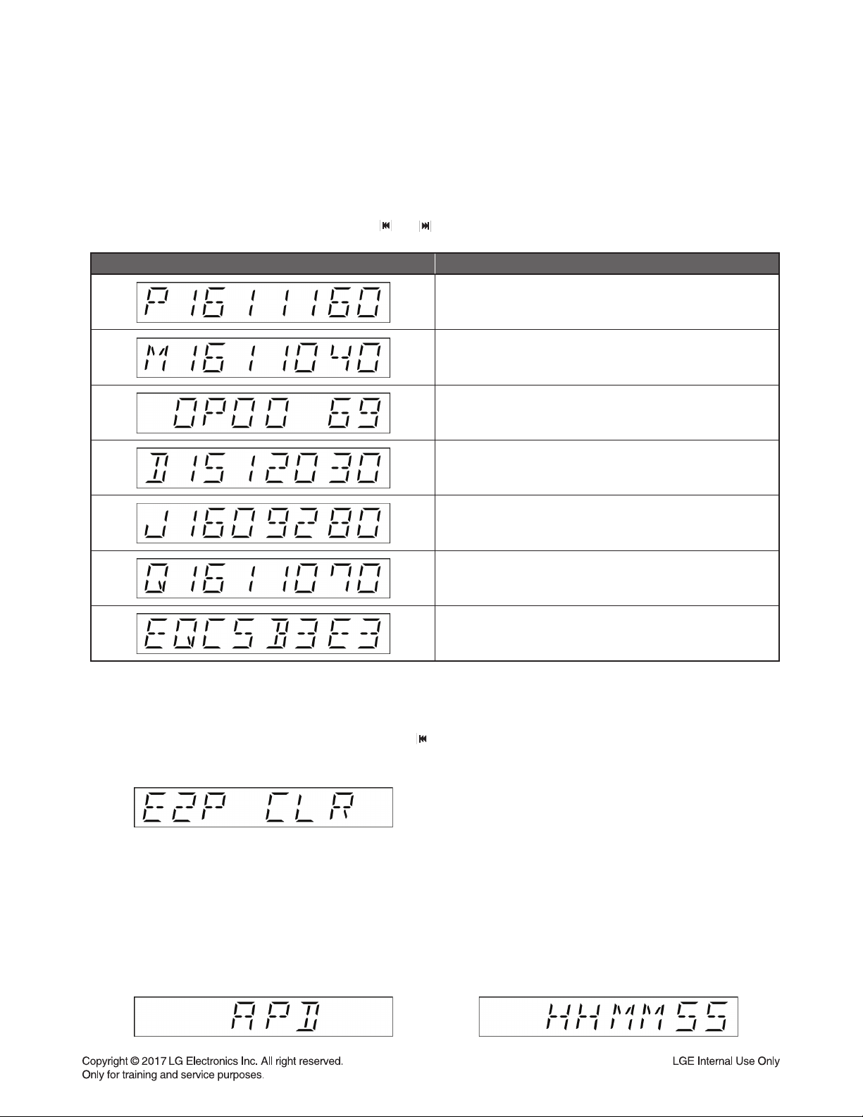
1. HIDDEN KEY MODE TABLE
HIDDEN KEY MODE
/
/
Page 8
1-7
2. HIDDEN KEY MODE DESCRIPTION
2-1. Version Check
- Function : Version Check.
- Entrance Key : Front ‘Stop’ + Remote Control Key ‘Play’ for 5s.
- Exit Key : Remote Control Key ‘Play’ for 1.5s.
- Operation explanation : Remote Control Key OR .
VFD Display (Example) Result
MCS Version
MICOM Version
OPTION Version
DEMO Version
DJ PRO Version
EQ Version
EQ Check sum Version
2-2. EEPROM Initial
- Function : Initialize data stored in EEPROM and BACKUP RAM data.
- Entrance Key : Front ‘Stop’ + Remote Control Key ‘ ‘ for 5s.
- Exit Key : Auto exit.
- Explanation : ‘E2P CLR’ is displayed on the VPD and turn off the power automatically.
2-3. OPTION EDIT (EEPROM)
- Refer to the page 00.
2-4. APD Test Display
- Function : Auto Power Down timer is displayed on VFD.
- Entrance Key : Front ‘Stop’ + Remote Control Key ‘3’ for 5s.
- Exit Key : Auto Exit.
- Explanation : display APD Timer HH=(hour) MM=(min), SS=(sec).
Page 9
1-8
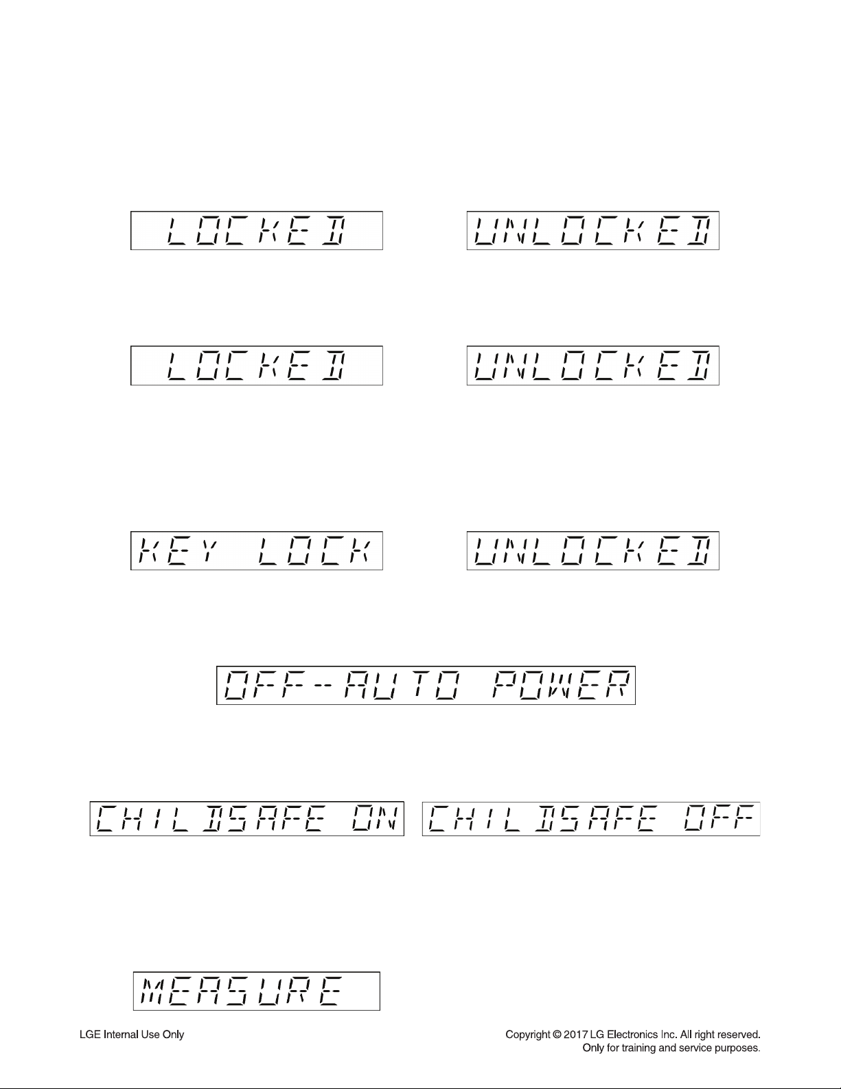
2-5. Disc Lock On/Off
- Function : Lock Open Key.
- Entrance Key : Front ‘Stop’ + Remote Control Key ‘Stop’ for 5s.
- Exit Key : Front ‘Stop’ + Remote Control Key ‘Stop’ for 5s.
- Operation Explain : Open Key Block ‘LOCKED’.
2-6. Power Disc Lock On/Off
- Function : Lock Power / Open / Front Volume Key.
- Entrance Key : Front ‘Stop’ + Front ‘Open’ for 5s.
- Exit Key : Front ‘Stop’ + Front ‘Open’ for 5s.
2-7. Demo All Key Lock
- Function : All key is blocked on Demo Mode.
- Entrance Key : Front ‘Stop’ + Remote Control Key ‘9’ for 5s.
- Exit Key : Front ‘Stop’ + Remote Control Key ‘9’ for 5s.
- Operation Key : In demo mode, all key blocks.
(only the volume key is effective when All Key Lock is enabled.)
To release Demo Mode, it is available after All Key Lock Off.
2-8. BT Auto Power On/Off
- Function : Ability to disable BT Auto Power On function by network shutdown regulation.
- Entrance Key : Front/Remote Control Key ‘Power’ for 5s.
- Exit Key : SET Power Off with Front / Remote Control Key ‘Power’.
2-9. ChildSafe On/Off
- Function : Power off Fade-in to previous volume.
- Entrance Key : Volume 0(Min) + Front ‘OK’ for 3s.
- Exit Key : Volume 0(Min) + Front ‘OK’ for 3s.
2-10. Measure
- Function : Change to EQ for Measure mode,
Down algorithm operation Disable,
Change to output setting value for measure mode.
- Entrance Key : Front ‘Stop’ + Remote Control Key ‘1’ for 5s
- Exit Key : Remote Control Key ‘SOUND EFFECT’
Page 10
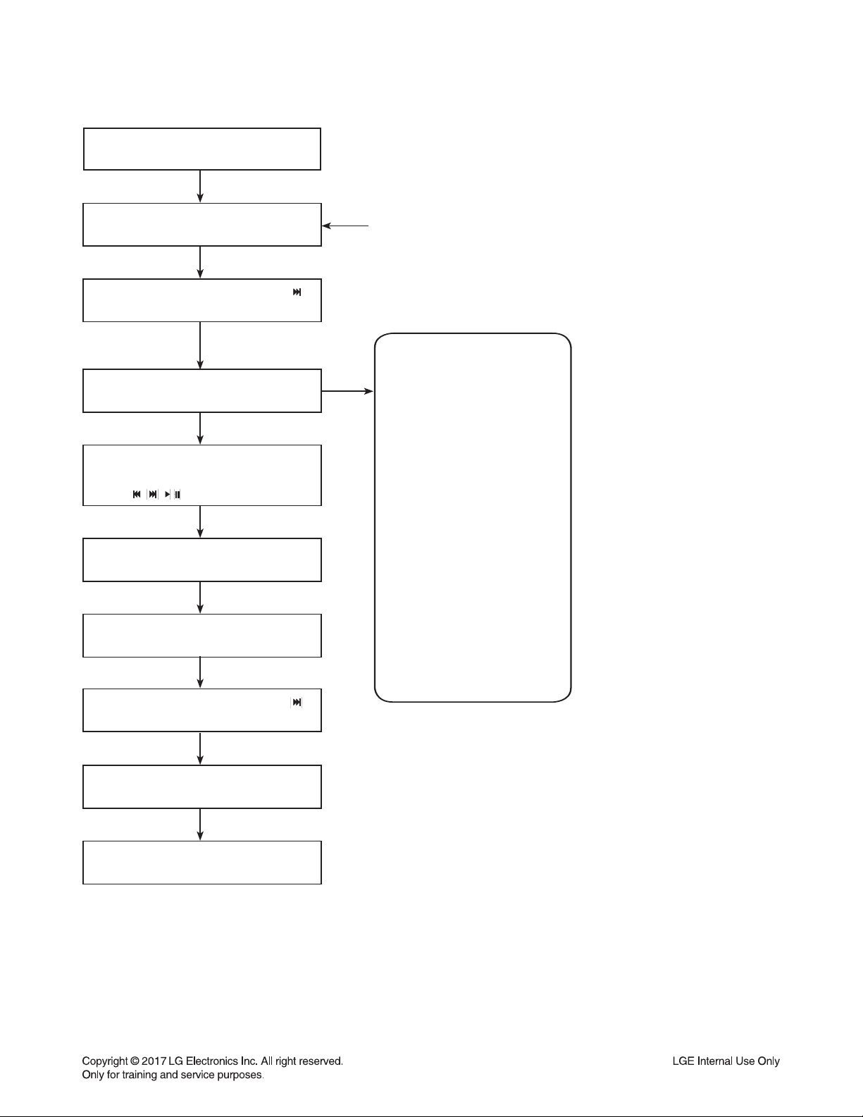
POWER ON
VFD “NO DISC” status
It is possible at any function.
(ex. It is possible at VFD “NO USB” status, too.)
This is an example.
Front ‘Stop’ + Remote control ‘ ’
push same timing during 5 s
FLD “OP00-…..”
Move to appropriate position
And make changes with remote control
“ , , , REPEAT” key.
Press ‘Stop’ Key
VFD “WRITE OK”
Front ‘Stop’ + Remote control ‘ ’
push same timing during 5 s
VFD “E2P CLR”
Completed
1-9
SERVICE INFORMATION FOR EEPROM
/
NAME
OPT0
OPT1
OPT2
OPT3
OPT4
OPT5
OPT6
OPT7
OPT8
OPT9
OPT10
OPT11
OPT12
OPT13
OPT14
DETECT NEW EEPROM
(OPTION EDIT SCREEN)
HEX
01
31
2D
26
49
00
00
43
4A
36
35
00
00
00
00
HEX
01
31
2D
26
49
00
00
43
4A
36
35
00
00
00
00
(LGEAP)
(LGEUS)
Page 11
1. CD PROGRAM
Download program file name must be HG740_CJ65_YYMMDDX.bin
If security program(Water Wall) is activated on PC, you must save the file to the USB storage device
and disable the security software, then download the file to your set.
Downloading file proceeds in the same way at USB1 function and USB2 function.
Caution:
When downloading the file, you should neither unplug the USB device, change to the other function,
nor power off the device. USB device must be unplugged when the downloading process is completed.
ON VFD DISPLAY SCREEN
1) (Fast) Format USB device.
2) Copy Firmware file to USB device.
NO USB
Insert USB device at USB function.
SEARCH
MICOM UP
FINISH
AUTO POWER OFF
1-10
PROGRAM DOWNLOAD GUIDE
Page 12
2. EQ & DEMO PROGRAM
Download program file name must be EQ_PRG.BIN
If security program(Water Wall) is activated on PC, you must save the file to the USB storage device
and disable the security software, then download the file to your set.
Downloading file proceeds in the same way at USB1 function and USB2 function.
Caution:
When downloading the file, you should neither unplug the USB device, change to the other function,
nor power off the device. USB device must be unplugged when the downloading process is completed.
ON VFD DISPLAY SCREEN
1) (Fast) Format USB device.
2) Copy Firmware file to USB device.
NO USB
Insert USB device at USB function.
SEARCH
EQDEMOUP
FINISH
AUTO POWER OFF
1-11
Page 13
1-12
FOTA UPDATE STEP USING BT APP
Step1 : App connecting
(Check FW version)
After connecting the BT App with SET,
the user could fi nd the “Device Version info” on
Setting tab.
Step3 : Select update button
When touch the “Update” button, user could
update the SET fi rmware using FOTA.
Step2 : Device version info
When touch the “Device Version info” button,
user could fi nd the current and latest SET
version on pop-up menu.
Step4 : Confi rm update
Select the OK button on the caution message.
Page 14
1-13
Step5 : Download from CDN server
1st step is download from CDN server to
smart phone. The progress bar is displayed
on BT App.
Step7 : FW Flash Writing Step8 : FOTA complete
After completed the download from the smart
phone, the SET overwrite the fi rmware to fl ash
memory.
When fi nishing the fl ash memory writing, pop-up
message about fi nish is displayed and the SET
auto power off.
Step6 : Transfer FW
After completed the download from server,
smart phone start to transfer the fi rmware to the
SET. The progress bar is displayed on BT App.
Page 15

SPECIFICATIONS
1-14
• GENERAL
Power requirements Refer to the main label on the unit.
Power consumption Refer to the main label on the unit.
Networked standby : 0.5 W
(If all network ports are activated.)
Dimensions (W x H x D) Approx. 350 mm x 163 mm x 251 mm
Operating temperature 5 °C to 35 °C (41 °F to 95 °F)
Operating humidity 60 %
• INPUTS
Analog audio in (AUX IN) 2.0 Vrms (1 kHz, 0 dB), 75 Ω, RCA jack (L, R)
Portable in (PORT.IN) 1.0 Vrms (3.5 mm stereo jack) x 1
Microphone (MIC) Sensitivity 20 mV (1 kHz), 6.3 mm jack x 1
• TUNER
FM Tuning Range 87.5 to 108.0 MHz or 87.50 to 108.00 MHz
AM Tuning Range 522 to 1,620 kHz, 520 to 1,710 kHz or 522 to 1,710 kHz
• SYSTEM
Frequency Response 70 to 20,000 Hz
Signal-to-noise ratio More than 75 dB
Dynamic range More than 75 dB
Bus Power Supply (USB) 5 V 500 mA
• AMPLIFIER (RMS Output power)
Total 900 W RMS
Front 450 W RMS X 2 (3 Ω at 1 kHz, 20 % THD)
• FRONT SPEAKER
Type 2 Way 2 Speaker
Impedance 3 Ω
Rated Input Power 450 W RMS
Max. Input power 900 W RMS
Net Dimensions (W x H x D) Approx. 299 mm x 363 mm x 230 mm
• Design and specifications are subject to change without notice.
Page 16

SECTION 2
CABINET & MAIN CHASSIS
CONTENTS
EXPLODED VIEWS ......................................................................................................................................... 2-3
1. CABINET AND MAIN FRAME SECTION ................................................................................................. 2-3
2. PACKING ACCESSORY SECTION ......................................................................................................... 2-7
3. SPEAKER SECTION ................................................................................................................................ 2-8
DISASSEMBLY INSTRUCTIONS ................................................................................................................... 2-9
1. Case Top ................................................................................................................................................... 2-9
2. Bracket ...................................................................................................................................................... 2-9
3. Panel Rear .............................................................................................................................................. 2-10
4. MAIN Board & SMPS Board ................................................................................................................... 2-11
5. Main PCB & SMPS PCB ......................................................................................................................... 2-12
6. Panel PCB & Multi Knob ......................................................................................................................... 2-13
7. Bracket SMPS ......................................................................................................................................... 2-14
8. MD ........................................................................................................................................................... 2-14
2-1
Page 17
2-2
Page 18
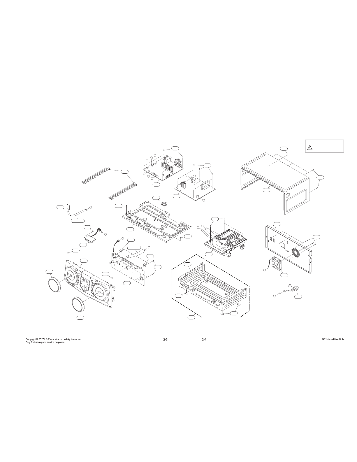
EXPLODED VIEWS
1. CABINET AND MAIN FRAME SECTION (CJ65)
D
A
B
MIC
262
BT
265
265
252
252
A42
H
300
498
A52
C
F
CABLE2
A00
254
254
443
E
FRONT
A43
266
443
G
443
274
443
263
498
443
443
264
443
443
D
E
F
G
C
B
A
A47
273
A46
443
MAIN
SMPS
443
H
CABLE1
A45
272
A44
NOTES) THE EXCLAMATION POINT WITHIN AN
EQUILATERAL TRIANGLE IS INTENDED
TO ALERT THE SERVICE PERSONNEL
TO THE PRESENCE OF IMPORTANT
SAFETY INFORMATION IN SERVICE
LITERATURE.
Page 19
Page 20
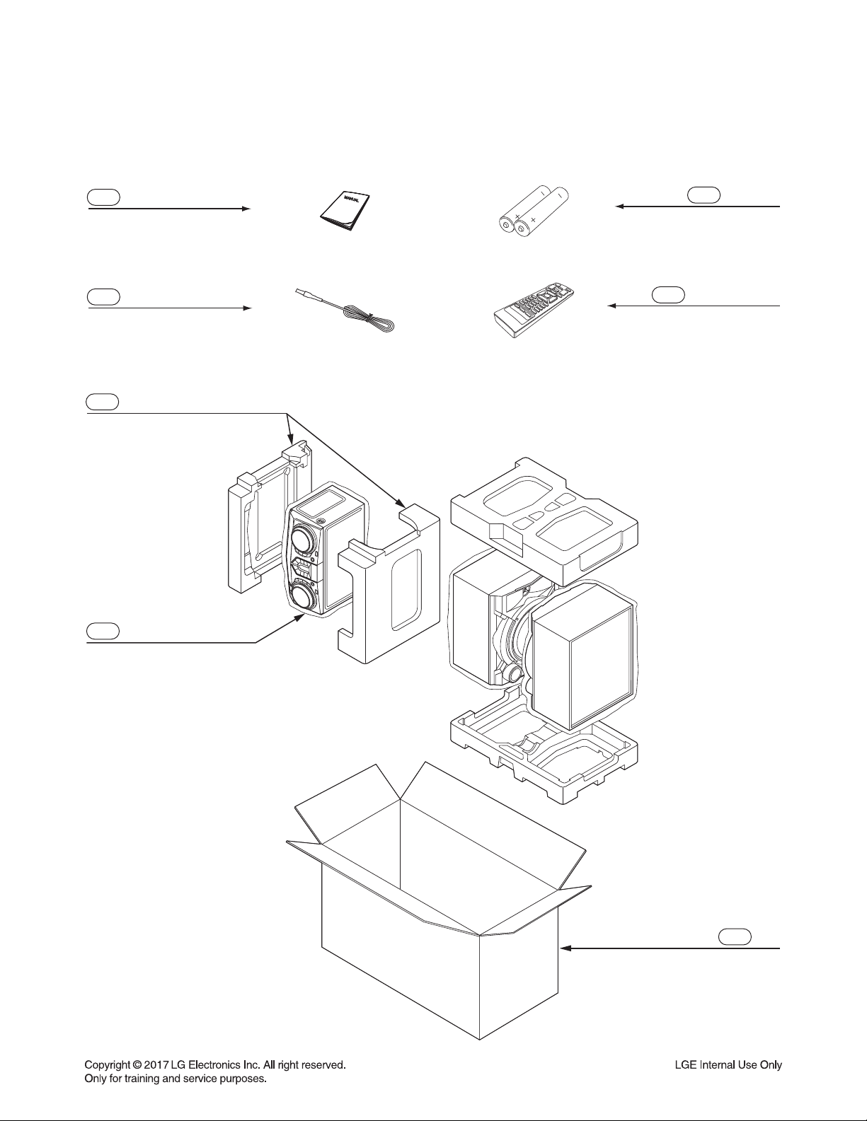
2-7
900 Remote control
808 Batteries
825 FM antenna
801 Owner’s manual
802 Box
804 Bag
Packing
803
2. PACKING ACCESSORY SECTION
Page 21

2-8
A60
3. SPEAKER SECTION
• FRONT SPEAKER (CJS65F)
Page 22

2-9
DISASSEMBLY INSTRUCTIONS
Figure 1
Figure 2
1. Case Top
1-1) Remove the 5 Screws.
1-2) Remove the Case Top.
2. Bracket
2-1) Remove the two Brackets between Front & Back Panel.
You can easily remove the Bracket after the hook detach from Front Panel.
Page 23

2-10
2
1
2
Figure 3
3. Panel Rear
3-1) Remove the 4 Screws from the Panel Rear.
3-2) Remove the Power Cord & FAN Cable from the SMPS Board.
3-3) Remove the Panel Rear.
Page 24

2-11
1
3
2
2
Figure 4
4. MAIN Board & SMPS Board
4-1) Remove the 9 Screws from the MAIN Board & SMPS Board.
4-2) Remove the 6 Cables from the MAIN Board.
4-3) Remove the Power Cord from the SMPS Board.
4-4) Remove the MAIN Board & SMPS Board.
Page 25

2-12
Figure 5
5. Main PCB & SMPS PCB
5-1) Remove the 2 Screws.
5-2) Unhook the 5 Locking Tabs by using Flat-head screwdriver.
5-3) Remove the Panel Front Assembly.
Page 26

2-13
(H1)
(H1)
(H1)
2
2
(L2)
(L2)
(L2)
(L2)
(L2)
(L2)
(H1)
(H1)
(H1)
1
(L1)
Figure 6
6. Panel PCB & Multi Knob
6-1) Multi Knob
6-1-1) Insert a Flat-head screwdriver in the hole (H1).
6-1-2) Remove the Multi Knob.
6-2) Jack PCB
6-2-1) Remove the 2 Screws.
6-2-2) Remove the Jack PCB.
6-3) BT Module
6-3-1) Unhook the Locking tab (L1).
6-3-2) Remove the BT Module.
6-4) Front PCB
6-4-1) Remove the 7 Screws.
6-4-2) Unhook the 2 Locking tabs (L2) from the Panel PCB.
6-4-2) Remove the Front PCB.
Page 27

2-14
Figure 8
8. MD
8-1) Remove the 2 Screws from the MD.
8-2) Remove the MD.
Figure 7
7. Bracket SMPS
7-1) Remove the Bracket SMPS.
Page 28

SECTION 3
ELECTRICAL
CONTENTS
ONE POINT REPAIR GUIDE ............................................................................................................................3-2
1. NO POWER ............................................................................................................................................3-2
2. NO BOOTING WHEN POWER ON THE SET........................................................................................3-4
3. VFD IS NOT DISPLAYED WHEN POWER ON THE SET .....................................................................3-5
4. NO OPERATION OF MD ........................................................................................................................3-6
5. NO SOUND ...........................................................................................................................................3-11
ELECTRICAL TROUBLESHOOTING GUIDE .................................................................................................3-17
1. POWER (SMPS) ...................................................................................................................................3-17
2. MCS PART CHECK ..............................................................................................................................3-20
3. IC503(GD25Q80) CHECK ....................................................................................................................3-20
4. FLD DISPLAY CHECK .........................................................................................................................3-21
5. PWM MODULATION CHECK ...............................................................................................................3-22
6. POWER AMP PART CHECK ...............................................................................................................3-23
7. TUNER / AUX FUNCTION CHECK ......................................................................................................3-24
8. TUNER FUNCTION CHECK.................................................................................................................3-24
9. CD FUNCTION .....................................................................................................................................3-25
10. DOUBLE USB FUNCTION ...................................................................................................................3-26
WAVEFORMS OF MAJOR CHECK POINT ....................................................................................................3-27
WIRING DIAGRAM ..........................................................................................................................................3-29
BLOCK DIAGRAMS ........................................................................................................................................3-31
1. SYSTEM BLOCK DIAGRAM ................................................................................................................3-31
2. SMPS BLOCK DIAGRAM .....................................................................................................................3-33
3. POWER BLOCK DIAGRAM .................................................................................................................3-35
CIRCUIT VOLTAGE CHART ........................................................................................................................... 3-37
1. INPUT VOLTAGE OF ICs .....................................................................................................................3-37
2. INPUT VOLTAGE OF CONNECTORS .................................................................................................3-37
3. VOLTAGE OF CAPACITORS ...............................................................................................................3-38
PRINTED CIRCUIT BOARD DIAGRAMS .......................................................................................................3-39
1. SMPS P.C.BOARD ...............................................................................................................................3-39
2. MAIN P.C.BOARD ................................................................................................................................3-41
3. FRONT P.C.BOARD .............................................................................................................................3-43
4. MIC P.C.BOARD DIAGRAM .................................................................................................................3-45
3-1
Page 29

3-2
ONE POINT REPAIR GUIDE
1. NO POWER
If the unit doesn’t work by no power problem, repair the set according to the following guide.
1-1. FUSE & BRIDGE DIODE
1-1-1. Solution
Please check and replace F901, BD901, TH901 or TH903 on SMPS board.
1-1-2. How to troubleshoot (Countermeasure)
1) Check if the fuse F901 is open or short-circuit.
2) Check if the bridge diode BD901 is short-circuit by over current with a digital multi meter.
3) Check if the NTC thermistor TH901 or TH903 is normal or open.
1-1-3. Service hint (Any picture / Remark)
< F901 >
If F901 is not short-circuit,
replace it with a same specifi ca-
tions one.
< TH901 >
If TH901 is open,
replace it with a new one.
< BD901 >
If BD901 is short-circuit,
replace it with a new one.
Page 30

3-3
ONE POINT REPAIR GUIDE
NO POWER
If the unit doesn’t work by no power problem, repair the set according to the following guide.
1-2. D951
1-2-1. Solution
Please check and replace D951 on SMPS board.
1-2-2. How to troubleshoot (Countermeasure)
1) Check the anode-cathod voltage of D951 with a digital multi-meter, it is normally 0.2 ~ 0.3 V.
If it doesn’t have any voltage, it’s destroyed. Replace it with a new one.
1-2-3. Service hint (Any picture / Remark)
< SMPS schematic diagram >
Page 31

3-4
ONE POINT REPAIR GUIDE
2. NO BOOTING WHEN POWER ON THE SET
The set doesn’t work when press the power button on the front board or the remote control.
2-1. FLASH MEMORY
2-1-1. Solution
Please check and replace IC501 on MAIN board.
2-1-2. How to troubleshoot (Countermeasure)
1) Check 12VA to CN102 in standby mode.
If there is no 12 VA, check the SMPS.
2) Check 12VA and PVDD when power on the set.
-
If the set doesn’t work regardless of what the KEY2 changes high to low while pressing the power button.
X500 and X501 work normally but, if you can not power on the set, replace IC500 with a new one on
the MAIN board.
2-1-3. Service hint (Any picture / Remark)
< Signal check point >
Page 32

3-5
ONE POINT REPAIR GUIDE
3. VFD IS NOT DISPLAYED WHEN POWER ON THE SET
When power on the set, any icons or characters on VFD are not displayed.
3-1. VFD
3-1-1. Solution
Please check and replace VFD300 on FRONT board.
3-1-2. How to troubleshoot (Countermeasure)
1) Check if 12 VA is output from SMPS to VFD via the MAIN board.
2) Check if Check if LED_5 V, DVCC_3 V output from the MAIN board.
3) Check if IC500 outputs VFD_D0, VFD_CLK and VFD_STB to the FRONT board.
4) Check if VFD300 output SW signal to the FRONT board.
If the SW signal isn’t output, replace VFD300 with new one.
5) check if Q300 and Q301 to the FRONT board.
If the VH signal isn’t output, replace Q300, Q301 with new one.
If the VH signal is output, replace VFD300 with new one.
3-1-3. Service hint (Any picture / Remark)
< Waveform of GR and SG signal >
Page 33

3-6
ONE POINT REPAIR GUIDE
4. NO OPERATION OF MD
When no sound output in the CD function, you can not listen to music reading data from a CD disc if
the servo motors in MD don’t work. This step is for checking the SPINDLE MOTOR among them.
4-1. SPINDLE MOTOR
4-1-1. Solution
Please check and replace IC400, IC401 on MAIN board.
4-1-2. How to troubleshoot (Countermeasure)
1) Check the SPDO signal from pin24 of IC401.
If no signal, check 3.3 V(RF) and X400.
2) Check the SPIN- & SPIN+ from IC400 to CN401 for driving SPINDLE motor. It is about 3.6 Vp-p.
If no signal, check +1.8 V and +5 V for IC401.
3) Check if the FFC cable is solidly connected between CN401 and MD.
4) Check the MD.
If the spindle motor is sort-circuit or has any trouble, it can not rotate CD discs.
Please check the function after changing another MD.
4-1-3. Service hint (Any picture / Remark)
About 3.6 Vpp
< Waveform of SP- & SP+
for driving SPINDLE motor >
< Signal check point >
Page 34

3-7
ONE POINT REPAIR GUIDE
< Signal check point >
NO OPERATION OF MD
When no sound output in the CD function, you can not listen to music reading data from a CD disc if
the servo motors in MD don’t work. This step is for checking the SLED MOTOR among them.
4-2. SLED MOTOR
4-2-1. Solution
Please check and replace IC400, IC401 on MAIN board.
4-2-2. How to troubleshoot (Countermeasure)
1) Check the SLDO signal from Pin23 of IC400.
If no signal, check 3.3 V(RF) and X400.
2) Check the SLED+ & SLED- from IC401 to CN401 for driving SPINDLE motor. It is about 2.9 Vp-p.
If no signal, check +1.8 V and +5 V for IC401.
3) Check if the FFC cable is solidly connected between CN401 and MD.
4) Check the MD.
If the sled motor is sort-circuit or has any trouble, it can not move the pickup module.
Please check the function after changing another MD.
4-2-3. Service hint (Any picture / Remark)
SL- TO CN401
SL+ TO CN401
< Waveform of SLED- & SLED+
for driving SLED motor >
Page 35

3-8
ONE POINT REPAIR GUIDE
NO OPERATION OF MD
When no sound output in the CD function, you can not listen to music reading data from a CD disc if
the servo motors in MD don’t work. This step is for checking the TRAY OPEN / CLOSE MOTOR among
them.
4-3. TRAY OPEN / CLOSE MOTOR
4-3-1. Solution
Please check and replace IC400, IC401 on MAIN board.
4-3-2. How to troubleshoot (Countermeasure)
1) Check MOT_OPEN & MOT_CLOSE signals from Pin K4, L4 of IC500 to IC400.
If no signal, check +1.8 V & + 5 V to IC401.
2) Check LOAD± from IC401 to CN401 for driving the tray open / close motor. It is about 3.85 Vp-p.
If no signal, check +5 V to IC401. If it has any trouble, replace it with a new one.
3) Check if the FFC cable is solidly connected between CN401 and MD.
4) Check the MD.
If the tray motor is sort-circuit or has any trouble, it can not open or close the tray.
Please check the function after changing another MD.
4-3-3. Service hint (Any picture / Remark)
LO- TO CN401
LO+ TO CN401
MOT_OPEN
CLOSE
< Waveform for driving
TRAY open / close motor >
< Signal check point >
Page 36

3-9
ONE POINT REPAIR GUIDE
NO OPERATION OF MD
When no sound output in the CD function, you can not listen to music reading data from a CD disc if
the pickup module in MD doesn’t work. This step is for checking the LASER TRACKING ACTUATOR.
4-4. LASER TRACKING ACTUATOR
4-4-1. Solution
Please check and replace IC400, IC401 on MAIN board.
4-4-2. How to troubleshoot (Countermeasure)
The tracking actuator makes the laser beam be positioned in the center of a track on CD disc.
1) Check the TRD signal from Pin22 of IC400.
If no signal, check 3.3 V(RF) and X400.
2) Check TR- & TR+ from IC408 to CN401 for driving the tracking actuator.
If no signal, check +1.8 V and +5 V for IC408.
3) Check if the FFC cable is solidly connected between CN401 and MD.
4) Check the MD.
If the pickup module has any trouble, it can not move the laser beam on the left or right side.
Please check the function after changing another MD.
4-4-3. Service hint (Any picture / Remark)
< Waveform of TR±
for driving TRACKING actuator >
< Signal check point >
Page 37

3-10
ONE POINT REPAIR GUIDE
NO OPERATION OF MD
When no sound output in the CD function, you can not listen to music reading data from a CD disc if
the pickup module in MD doesn’t work. This step is for checking the LASER FOCUSING ACTUATOR.
4-5. LASER FOCUSING ACTUATOR
4-5-1. Solution
Please check and replace IC400, IC401 on MAIN board.
4-5-2. How to troubleshoot (Countermeasure)
The focusing actuator makes the laser beam keep a regular interval with the surface of a CD disc.
1) Check the FOD signal from Pin21 of IC400.
If no signal, check 3.3 V(RF) and X400.
2) Check F- & F+ from IC408 to CN401 for driving the focusing actuator.
If no signal, check +1.8 V and +5 V for IC401.
3) Check if the FFC cable is solidly connected between CN401 and MD.
4) Check the MD.
If the pickup module has any trouble, it can not move the laser beam on the top or bottom side.
Please check the function after changing another MD.
4-5-3. Service hint (Any picture / Remark)
< Waveform of F±
for driving FOCUSING actuator >
< Signal check point >
Page 38

3-11
ONE POINT REPAIR GUIDE
5. NO SOUND
There is no sound output in the CD FUNCTION, repair the set according to the following guide.
5-1. IN THE CD FUNCTION
5-1-1. Solution
Please check and replace IC501, IC601 on MAIN board.
5-1-2. How to troubleshoot (Countermeasure)
1) Check CD_BCLK, CD_LRCK, & CD_DOUTA signals from IC401 to IC500.
If no signal, check if the RF & servo signals from MD is entered to IC401.
Refer to the “No operation of MD” guide on Item 4.
2) Check the following I2S signal flow. < I2S audio signal Interface >
- ADC_BCK : IC500_Pin E1 --> IC700_Pin23
- ADC_LRCK : IC500_Pin D1 --> IC700_Pin22 (44.1 kHz)
- MIX_DATA_0 : IC500_Pin E2 --> IC700_Pin24
- MIX_DATA_1 : IC500_Pin R2 --> IC700_Pin25
- ADC_MCLK : IC500_Pin D2 --> IC700_Pin44
If there is any trouble, check the power for each IC. The power is normal but, if the signal waveform to
the IC is distorted or no signal, replace it with a new one.
3) Check if “Digital audio AMP block” on Item 5-2 is normal.
5-1-3. Service hint (Any picture / Remark)
MCS_MCLK (16.93 MHz)
MCS_BCK(1.4 MHz)
MCS_DATA_OUT
MCS_LRCK(44.1 KHz)
< Waveform of I2S audio interface signals >
< I2S Signal Flow >
M
P/UP
PWM
TAS5548
TAS5624LA
FR,FL
12.288 MHZ
IC401
DSP IC500
176 PIN
BGA
Interrupt
controller
CDROM x8 speed
Decoder
NAND Controller
within BCH codec
14bits ECC
GDMA 3ch
ADC (12bit*5ch)
Timer, Watchdog
GPIO (72 Max)
SPI 4ch (Max)
RTC & Wake up
UART 4ch (Max)
I2C 2ch
SDHC-SDIO 4ch (Max)
USB 2.0 OTG
SRAM (10K)
Main Processor
Audio DSP-0
GDMA 2ch
I2S (7.1ch)
SPDIF (Rx, Tx)
ADPCM
PLL
Clock Controller
Reset Controller
Test Controller
Audio DSP-1
USB 1.1
Host/Device
ARM
926EJS
16KB
I-Cache
16KB
D-Cache
400Mhz
DSP
133Mhz
SRAM29KB
I-Cache 8KB
D-Cache 8KB
DSP
133Mhz
SRAM29KB
I-Cache 8KB
D-Cache 8KB
Boot ROM (20KB)
SDRAM
Controller
Page 39

3-12
ONE POINT REPAIR GUIDE
NO SOUND
There is no sound output by DIGITAL AUDIO AMP DAMAGE, repair the set according to the following
guide.
5-2. BY DIGITAL AUDIO AMP DAMAGE (IN ALL FUNCTIONS)
5-2-1. Solution
Please check and replace C744(IC701), C746(IC702) on MAIN board.
5-2-2. How to troubleshoot (Countermeasure)
1) Check PWM_FL±, PWM_FR± & PWM_SW± signals from IC700 to IC701 & 702 each input function.
If no signal, check if I2S audio signals are entered to IC700.
Refer to “I2S audio signal interface” on Item 5-1.
2) Check PVDD.
If PVDD is abnormal, check the SMPS.
3) Check +12 V for driving the gate of AMP IC.
a. All the powers are normal, but if +12 V is low, there is possible for AMP IC to be damaged.
b. Remove C742, C746(IC702), C740, C744(IC701) one by one.
When removed a inductance, if +12 V is recovered, the IC connected to it was damaged.
c. Replace the IC with a new one.
4) Check the impedance between IC701/IC702_OUT_A/OUT_B/OUT_C/OUT_D & GND.
a. If the impedance is 0 Ω, the IC must be damaged.
b. After removing the heat sink, replace it with a new one.
5-2-3. Service hint (Any picture / Remark)
< Signal check point >
Page 40

3-13
ONE POINT REPAIR GUIDE
NO SOUND
There is no sound output in the USB FUNCTION, repair the set according to the following guide.
5-3. IN THE USB FUNCTION
5-3-1. Solution
Please check and replace IC500 on MAIN board & IC104 on USB board.
5-3-2. How to troubleshoot (Countermeasure)
1) Check +5V_USB to USB board.
If the USB LED are turned on, the voltage is okay, if so not, check +5.6 V to pin6 of CN502.
2) Check USB D1± or USB D2± from MAIN board to USB board.
a. Check 2.0_D1±signals(pin U7, U8 ) or 1.1_D1± signals(pin A7, A8 ) to IC500.
b. Check USB± signals to CN502(pin1, 2, 4, 5).
If there is any trouble, check the power for each IC. The power is normal but , if the signal waveform to
the IC is distorted or no signal, replace it with a new one.
3) Check if “Digital audio AMP block” on item 5-2 is normal.
5-3-3. Service hint (Any picture / Remark)
D- to pin 1&4 of CN502
D+ to pin 2&5 of CN502
< Waveform of USB D± signal >
< USB function signal fl ow >
PWM
FR,FL
12.288 MHZ
DSP IC500
176 PIN
USB1_D±
USB2_D±
Interrupt
controller
CDROM x8 speed
Decoder
NAND Controller
within BCH codec
14bits ECC
GDMA 3ch
ADC (12bit*5ch)
Timer, Watchdog
GPIO (72 Max)
SPI 4ch (Max)
RTC & Wake up
UART 4ch (Max)
I2C 2ch
SDHC-SDIO 4ch (Max)
USB 2.0 OTG
SRAM (10K)
Main Processor
Audio DSP-0
GDMA 2ch
I2S (7.1ch)
SPDIF (Rx, Tx)
ADPCM
PLL
Clock Controller
Reset Controller
Test Controller
Audio DSP-1
USB 1.1
Host/Device
ARM
926EJS
16KB
I-Cache
16KB
D-Cache
400Mhz
DSP
133Mhz
SRAM29KB
I-Cache 8KB
D-Cache 8KB
DSP
133Mhz
SRAM29KB
I-Cache 8KB
D-Cache 8KB
Boot ROM (20KB)
SDRAM
Controller
Page 41

3-14
ONE POINT REPAIR GUIDE
NO SOUND
There is no sound output in the AUX FUNCTION, repair the set according to the following guide.
5-4. IN THE AUX FUNCTION
5-4-1. Solution
Please check and replace IC202 on MAIN board.
5-4-2. How to troubleshoot (Countermeasure)
1) Check AUX_L/R signals to IC202 (Pin29, 30).
2) Check if MCS_BCK, MCS_LRCK & MCS_MCLK are entered from IC500 to IC202.
3) Check if ADC_DATA is entered from IC202 to IC500.
If no signal, check +5 V & +3.3 V(ADC) for IC201. If is NG, replace it a new one.
4) Check the following I2S signal flow from IC801 to IC602. (Refer to Item 5-1.)
If there is any trouble, check the power for each IC. The power is normal but, if the signal waveform to
the IC is distorted or no signal, replace it with a new one.
5) Check if the digital audio AMP block is okay. Refer to “Digital Audio AMP” guide on Item 5-2.
If AMP is damaged, replace it with a new one.
5-4-3. Service hint (Any picture / Remark)
< AUX function signal fl ow >
PWM
FR,FL
12.288 MHZ
DSP IC500
176 PIN
IC202
AUX
AUX _L /R
Interrupt
controller
CDROM x8 speed
Decoder
NAND Controller
within BCH codec
14bits ECC
GDMA 3ch
ADC (12bit*5ch)
Timer, Watchdog
GPIO (72 Max)
SPI 4ch (Max)
RTC & Wake up
UART 4ch (Max)
I2C 2ch
SDHC-SDIO 4ch (Max)
USB 2.0 OTG
SRAM (10K)
Main Processor
Audio DSP-0
GDMA 2ch
I2S (7.1ch)
SPDIF (Rx, Tx)
ADPCM
PLL
Clock Controller
Reset Controller
Test Controller
Audio DSP-1
USB 1.1
Host/Device
ARM
926EJS
16KB
I-Cache
16KB
D-Cache
400Mhz
DSP
133Mhz
SRAM29KB
I-Cache 8KB
D-Cache 8KB
DSP
133Mhz
SRAM29KB
I-Cache 8KB
D-Cache 8KB
Boot ROM (20KB)
SDRAM
Controller
< Signal check point >
Page 42

3-15
ONE POINT REPAIR GUIDE
NO SOUND
There is no sound output in the TUNER FUNCTION, repair the set according to the following guide.
5-5. IN THE TUNER FUNCTION
5-5-1. Solution
Please check and replace IC202, TU200 on MAIN board.
5-5-2. How to troubleshoot (Countermeasure)
1) Check if TUNER_LR is entered from Pin1, 3 of TU200 to IC202(Pin27, 28).
If no signals, check +3.3 V for tuner power.
Check if the tuner control signals (CLK, DAT, CE, RST, SLT) are entered from IC500 to TU200.
If it doesn’t work, replace TUNER with a new one.
2) Check if MCS_BCK, MCS_LRCK, & MCS_MCLK are entered from IC500 to IC202.
3) Check if ADC_DATA is entered from IC202 to IC500.
If no signal, check +5 V & +3.3 V(ADC) for IC202. If is NG, replace it with a new one.
4) Check the following I2S audio signal flow from IC500 to IC700. (Refer to Item 5-1.)
If there is any trouble, check the power for each IC. The power is normal but, if the signal waveform to
the IC is distorted or no signal, replace it with a new one.
5) Check if the digital audio AMP block is okay. Refer to “Digital Audio AMP” guide on Item 5-2.
If AMP is damaged, replace it with a new one.
5-5-3. Service hint (Any picture / Remark)
< TUNER IN function signal fl ow >
PWM
FR,FL
12.288 MHZ
DSP IC500
176 PIN
BGA
IC202
TUNER_ L/R
TUN ER
A
Interrupt
controller
CDROM x8 speed
Decoder
NAND Controller
within BCH codec
14bits ECC
GDMA 3ch
ADC (12bit*5ch)
Timer, Watchdog
GPIO (72 Max)
SPI 4ch (Max)
RTC & Wake up
UART 4ch (Max)
I2C 2ch
SDHC-SDIO 4ch (Max)
USB 2.0 OTG
SRAM (10K)
Main Processor
Audio DSP-0
GDMA 2ch
I2S (7.1ch)
SPDIF (Rx, Tx)
ADPCM
PLL
Clock Controller
Reset Controller
Test Controller
Audio DSP-1
USB 1.1
Host/Device
ARM
926EJS
16KB
I-Cache
16KB
D-Cache
400Mhz
DSP
133Mhz
SRAM29KB
I-Cache 8KB
D-Cache 8KB
DSP
133Mhz
SRAM29KB
I-Cache 8KB
D-Cache 8KB
Boot ROM (20KB)
SDRAM
Controller
< Signal check point >
Page 43

3-16
ONE POINT REPAIR GUIDE
NO SOUND
There is no sound output in the PORTABLE FUNCTION, repair the set according to the following
guide.
5-6. IN THE PORTABLE FUNCTION
5-6-1. Solution
Please check and replace IC202 on MAIN board.
5-6-2. How to troubleshoot (Countermeasure)
1) Check PT_L/R signals to IC202 (Pin1, 2).
2) Check if MCS_BCK, MCS_LRCK, & MCS_MCLK are entered from IC500 to IC202.
3) Check if ADC_DATA is entered from IC202 to IC500.
If no signal, check +5 V & +3.3 V(ADC) for IC202. If NG, replace it a new one.
4) Check the following I2S signal flow from IC500 to IC700. (Refer to Item 5-1.)
If there is any trouble, check the power for each IC. The power is normal but, if the signal waveform to
the IC is distorted or no signal, replace it with a new one.
5) Check if the digital audio AMP block is okay. Refer to “Digital Audio AMP” guide on Item 5-2.
If AMP is damaged, replace it with a new one.
5-6-3. Service hint (Any picture / Remark)
< PORTABLE function signal fl ow >
PWM
FR,FL
12.288 MHZ
DSP IC500
176 PIN
IC202
Port able
PTB_L/R
Interrupt
controller
CDROM x8 speed
Decoder
NAND Controller
within BCH codec
14bits ECC
GDMA 3ch
ADC (12bit*5ch)
Timer, Watchdog
GPIO (72 Max)
SPI 4ch (Max)
RTC & Wake up
UART 4ch (Max)
I2C 2ch
SDHC-SDIO 4ch (Max)
USB 2.0 OTG
SRAM (10K)
Main Processor
Audio DSP-0
GDMA 2ch
I2S (7.1ch)
SPDIF (Rx, Tx)
ADPCM
PLL
Clock Controller
Reset Controller
Test Controller
Audio DSP-1
USB 1.1
Host/Device
ARM
926EJS
16KB
I-Cache
16KB
D-Cache
400Mhz
DSP
133Mhz
SRAM29KB
I-Cache 8KB
D-Cache 8KB
DSP
133Mhz
SRAM29KB
I-Cache 8KB
D-Cache 8KB
Boot ROM (20KB)
SDRAM
Controller
< Signal check point >
Page 44

1. POWER (SMPS)
No 5.6 VA
YES
F901 normal?
Replace F901 (Use the same fuse).
YES
NO
BD901 normal?
Replace BD901.
YES
NO
TH901(TH903) normal?
Replace TH901.
YES
NO
Is Vcc
(10 V ~ 18 V) supplied to
IC901 pin7?
Is there
about 2.5 V at IC951
pin1?
D902 normal?
Replace D951.
YES
NO
NO
Check or replace D902.
Is there
about 2.5 V at
IC941 Pin1?
Replace IC941.
YES
NO
D951 normal?
Replace D951.
YES
YES
NO
D933 normal?
Replace D933.
YES
NO
Power line of main PCB is short.
NO
3-17
ELECTRICAL TROUBLESHOOTING GUIDE
Page 45

No PVDD
YES
F901 normal?
Replace F901 (Use the same fuse).
YES
NO
BD901 normal?
Replace BD901.
YES
YES
NO
TH901(TH903) normal? Replace TH901.
YES
YES
NO
Is Vcc
(10 V ~ 18 V) supplied to
IC911 pin4?
D903 normal?
YES
NO
Check or replace D903.
• Check P-CTRL “H” signal from MCS.
• Check PC902.
Q901 normal?
Replace Q901.
Check or replace Q911.
YES
NO
D951 normal?
Replace D951.
YES
NO
Is there about 2.5 V
at IC951 pin1?
Replace IC951.
YES
NO
Q901 base “H”?
Power line of main PCB is short.
NO
NO
3-18
ELECTRICAL TROUBLESHOOTING GUIDE
Page 46

No 12 V
Is Vcc (15 V)
supplied to IC931?
Check or replace D935.
YES
YES
NO
IC931 pin4 “H”?
Check P-CTRL “H” signal from MCU.
YES
NO
Check or replace IC931.
No VFD
YES
D931 normal?
ZD931 normal?
Q300 / Q301 normal?
Check or replace D931.
Check or replace ZD931.
Check or replace Q300 / Q301.
YES
YES
YES
NO
NO
NO
Check or replace VFD.
3-19
ELECTRICAL TROUBLESHOOTING GUIDE
Page 47

3-20
3. IC503(GD25Q80) CHECK
CHECK IC500 PIN.
OKOK
Refer to MCS troubleshooting.
Replace MCS.
OKOK
Check
pinA12, pinB12 SF_SCK :
SF_MISO
Check MCS
voltage 3.3 VA.
Check MCS.
NO
NO
NO
YES
YES
YES
YES
ELECTRICAL TROUBLESHOOTING GUIDE
2. MCS PART CHECK
YES
YES
YES
YES
YES
MCS PART CHECK
OK
Refer to SMPS troubleshooting.
Check and change IC101.
X500: 24 MHz, X500: 32.768 kHz
Check the operation.
Check and change IC100.
NO
NO
NO
Check if voltage of CN102
Pin13, 14 is 12 VA.
Check if IC101
have 1.2 VA output.
Check if IC100
have 3.3 VA output.
Page 48

3-21
4. FLD DISPLAY CHECK
ELECTRICAL TROUBLESHOOTING GUIDE
FLD DISPLAY CHECK
OKOK
Check if both end voltage of F+, F- are over 1.85 V
VH : over 27 V.
Check CN300 connection.
If voltage isn’t over VH : 27 V, F- : 3 V
and, SW signal is not operation?
OK
Check output data IC500 Pin B3.
Check input data
IC500 Pin F2, B3, B1.
Replace IC500.
Replace VFD300.
Check each Pin voltage.
FLD light on?
OK
OKOK
Refer to SMPS troubleshooting.
Check
CN102 Pin13,14 input
voltage.
Check
CN300 connection and
power Pin14, 16,17
(VIN, F+, VDD).
Check
VFD300 voltage Pin27,
26, 31, 32 VH: over 27
V, SW Signal, F- : over
3 V is OK?
Check
IC500->VFD300 data
communication STB/
DATA/ CLK
Check VFD300.
Check IC500.
NO
NO
NO
NO
NO
NO
NO
YES
YES
YES
YES
YES
YES
YES
YES
YES
YES
YES
YES
YES
Page 49

3-22
ELECTRICAL TROUBLESHOOTING GUIDE
5. PWM MODULATION CHECK
PWM MODULATION PART
CHECK
• Check IC700(TAS5548) VDD 3.3 V - Pin9,14.35,50.
• Check X700 (12.288 MHz).
Replace X700(12.288 MHz).
Replace IC700.
Refer to CD troubleshooting.
Check each line resistor output.
OK
OK
OK
Check IC700 Pin21 CLK input.
Refer to
SMPS troubleshooting.
Check
CN102 Pin13, 14
(12 VA)
Check
X700(12.288 MHz)
operation.
Check
IC700(TAS5548) input
data Pin24, 25
PWM wave.
Check X700
(12.288 MHz).
Check IC700.
Check PWM
modulator output
FL: Pin48(-),49(+)
FR: Pin46(-),47(+).
Other output
check.
Check CD
Assy communication
Pin22, 23, 24.
Check
IC700 input
data.
NO
NO
NO
NO
NO
NO
NO
NO
YES
YES
YES
YES
YES
YES
YES
YES
YES
YES
YES
YES
OK
Page 50

3-23
ELECTRICAL TROUBLESHOOTING GUIDE
6. POWER AMP PART CHECK
YES
YES
YES
YES
YES
YES
YES
POWER AMP PART CHECK
OK
Refer to SMPS troubleshooting.
Check each line resistor output voltage.
Replace the coil.
Check IC701, IC702
Pin29, 30, 31, 36, 37, 38 input voltage.
Check PWM Modulator input
IC701 Pin14, 15 / IC702 Pin5, 6. 14, 15.
Check IC701, IC702
Pin27, 28, 32, 35, 39, 40.
NO
NO
NO
Check
CN102 Pin13, 14: +12 VA
Pin5, 6, 7 : 36 V.
Check IC701, IC702
Pin2: +12 V input.
Check output line coil.
Page 51

TUNER FUNCTION CHECK
Check tuner module(TU200)
operation.
Check tuner module voltage
(Pin4: +3.3 V).
YES
YES
NO
Check IC500 Pin P7, P8, P10, P11.
Check tuner module data.
YES
NO
Refer to function check.
8. TUNER FUNCTION CHECK
3-24
ELECTRICAL TROUBLESHOOTING GUIDE
7. TUNER / AUX FUNCTION CHECK
FUNCTION CHECK
Replace IC201.IC500(MLC3730) output data.
Check IC202
Pin18,19:ADC, MIC_DATA SDOUT,
Pin17: BCK, Pin16: LRCK,
Pin15: MCLK.
Check IC202
Pin8: ADC +3.3 V,
Pin13, 14, 25: DVCC +3.3 V.
Check CN102 Pin13,14: 12 VA.
Check JK200,TU200.
Check
IC500(MLC3730)
input data.
Check IC202
(PCM1865) Pin18, 19
output data.
Check
IC202 Pin8: ADC +3.3 V
Pin13,14,25: DVCC
+3.3 V.
Check IC202
(PCM1865) Pin27, 28,
29, 30 input.
NO
NO
NO
NO
NO
YES
YES
YES
YES
YES YES
YES
OK
Page 52

3-25
ELECTRICAL TROUBLESHOOTING GUIDE
9. CD FUNCTION
CD FUNCTION
Is Motor_open/close OK?
(IC400 Pin9,10)
Replace Cristal (X400).
Check loading motor.
Check IC400.
Check IC400
(Motor drive IC).
Is the MD(CN400 Pin7)
about 190 mV?
Check IM (pick-up).
IM driving
(Focus and tracking) is ok?
Check Vcc of IC401.
Replace IC500.
Check Cristal (X400).
Is Motor ok? (about 12 Ω)
Is no signal at spk?
Can the
disc insert?
Disc reading
is ok?
Check
the signal of IC401
Pin52,53,54.
Check IC500
input/output and
control line.
Check
the signal (16.9344
MHz) at IC401
Pin51.
Focus,
tracking, sled signal
is ok?
Is load +,- ok?
NO
NO
NO
NO
NO
NO
NO
NO
NO
YES
YES
YES
YES
YES
YES
YES
YES
YES
NO
YES
NO
Refer to function check.
Page 53

3-26
ELECTRICAL TROUBLESHOOTING GUIDE
10. DOUBLE USB FUNCTION
USB FUNCTION
Check USB jack
(JK301/ JK302).
Replace IC500.
Check CON301.
Check IC500
(Pin U7, U8/ A7, A8).
Display “NO FILE”.
Check USB_5 V.
Display “READ”.
Plug-in USB device.
Display “NO USB”.
Check USB_D-/D+
(R383, 384).
NO
NO
NO
NO
YES
YES
YES
YES
YES
YES
YES
Check USB audio file in USB device
(MP3, WMA file is playable)
Page 54

3-27
WAVEFORMS OF MAJOR CHECK POINT
CLK
DATA
ADDRESS
CS
CD-16 M
Fig 1. SDRAM
①IC504 pin38, ②IC504 pin53
③IC504 pin35, ④IC504 pin19
Fig 2. SERVO
⑤IC500 pin M1
1
2
3
4
CD_BCK
CD_LRCK
CD_DATA
MCS_MCLK
MCS_BCK
MCS_LRCK
ADC_DATA
Fig 3-1. AUDIO PATH
⑥IC500 pin N4, ⑦ICIC500 pin N1
⑧ICIC500 pin N2
Fig 3-2. AUDIO PATH
⑨IC500 pin D2, ⑩IC500 pin E1
⑪IC500 pin D1, ⑫IC500 pin E2
8
6
7
10
12
11
9
5
USB_5 V
D+
D-
Fig 4. USB
⑬IC500 pin A8, ⑭IC500 pin A7
14
13
Page 55

3-28
Page 56

3-29 3-30
ڜڜڨڐړڔٻ
ڤڞڐڋڋٻ
ڟڮګٻ
ڤڞڏڋڌٻ
ڭڡٻڤڞٻ
ڤڞڒڋڋٻ
ګڲڨٻ
ڤڞڍڋڍٻ
ڜڟڞٻ
ڤڞڐڋڎٻ
ڡڊڮٻڌڑڨٻ
ڤڞڐڋڏٻ
ڮڟڭڜڨٻ
ڤڞڏڋڋٻ
ڨۊۏۊۍٻڟڭٻ
گېۉۀۍٻ
ڨڤڞٻ
ګگڝٻ
ڰڮڝڌٻ
ڰڮڝڍٻ
ٻٻٻٻ ٻ ٻ ٻ ٻ
ٻ
ٻ
ٻ
ٻ
ٻ
ٻ
ٻ
ٻ
ٻ
ٻ
ٻ
ڨڜڤکٻ
ڝگٻ
ۈۊڿېۇۀٻ
ڜڰڳٻڤۉٻ
ڮڨګڮٻ
ڣڼۍۉۀێێٻ
ڡڡڞ
ٻٻٻٻ
ڡڧٻ
ڭڧٻ
ڥڜڞڦٻ
ڤڞڍڋڏٻ
ڠڳګڠکڟڠڭٻ
ڤڞڍڋڋٻ
ڎ
ګٻ
ڡڭڪکگٻ
ڌڏګٻڝٻگڪٻڝٻ
ړ
ګ
ٻ
ڌڏګ
ٻ
ڝ
ٻ
گڪٻڝٻ
ړ
ګ
ٻ
ړګٻ
ڰڮڝٻ
ڌڒګٻ
ڌڋګٻ
ړګٻ
ڰڮڝٻ
ڌڒګٻ
ڨڟٻ
ڌڋګ
ٻ
ڍڎګٻ
ڌڋګ
ٻ
ڍڎګٻ
ڮګڦںڭٻ
ڮګڦںڧٻ
jq[[⏈GmhuG㇡㥐G
WIRING DIAGRAM
Page 57

3-31 3-32
BLOCK DIAGRAMS
1. SYSTEM BLOCK DIAGRAM
ڤڤڞڐڋڋٻ
ڨڼۄۉٻڟڮګٻ
ٻ
ٻٻ
ڃچڎډڎڱںڞڟڇٻڱڞڞڌډڍڄٻ
ڟڠڞڦٻٻٻ
ڨڠڞڣڜکڤڮڨٻ
ڨٻ
ګڊڰګٻ
ڃڱڞڞڐڋڄٻ
ٻ
ٻ
گڪګٻ
ڝڧڪڞڦٻ
ڱۊۇېۈۀڊٻ
ڦۀ۔ڊێےۄۏھۃٻ
ڃچڎډڎڱڜڇڐڱڇچڌڍڱڄٻ
ڌڑڨڝٻ
ڮڟڭڜڨٻٻ
ڏڨڝٻ
ڡۇڼێۃٻ
ڤڞڏڋڋٻ
ڨۊۏۊۍٻڟۍۄۑۀٻ
ڰڮڝڌٻ
ڰڮڝڍٻ
ڤڞڏڋڌٻ
ڮڠڭڱڪٻڤڞٻ
ڤڞڍڋڍٻ
ڜڟڞٻ
ڟڭڨںڲڠکڊڞڜڮڊٻ
ڭڜڮڊڮڠڧڊڞڧڦڊڞڦڠٻ
ٻڮۋۀڼۆۀۍٻ
ڧۄۂۃۏۄۉۂٻ
ڜڟڞںڟڜگڜٻ
ڨڞڮںڝڞڦڊڧڭڞڦڊڨڞڧڦٻ
ڡڭڪکگڃڝگڧڄٻ
ڨڋڋںڌڐٻ
ڜڋڋںڌڑٻ
ڮڡںڟڤڊڟڪٻ
ڮڡںڞڮڊڮڞڦٻ
ڱڡڟںڮگڝڊڞڧڦڊڟڪڊڭڮگڇٻ
ڨڜڤکٻڱڪڧںڜڊڝڇٻ
ڦڠڴٻڌڊڍٻ
ڪګںڮڲڇڞڧںڮڲڇڰګںڮڲڇڟکںڮڲڇڟںڮڠکڮڠٻ
ڨڪگںڨڰگڠڇڞڧڪڮڠڇڪګڠکٻ
ڜڇڝڇڞڇڟڇڠڇڡڇګڟٻٻٻ
ڧڟٻ
ڮګڟڪڊڮڧڟڪٻ
ڊڡڪڟڊگڭڟٻ
ڧڪڜڟڇڮڧڠڟڇٻ
ڮګڤکڇگڭڇڡٻ
ڟڍڮچڊڈٻ
ګڲڨںڧڭڞڦڊڝڞڦڊڟڜگڜٻ
ڞڟںڭڲڊڨڞڧڦڊڧڭڞڦڊڝڞڦڇٻ
ڞڟںڟڜگٻ
ڞڟںڭڮگٻ
ڡۊۍٻڜڰڳٻ
ڌډڌٻڍډڋٻ
[CJ65 : Total 2hch 900W]
[CJ44 : Total 2ch 460W]
ڌڨڝٻ
ڮڊڡۇڼێۃٻ
ڮڡںڟڤڊڟڪٻ
ڮڡڍںڞڮڊڮڞڦٻ
ڜڰڳٻڤکٻ
گڰکڠڭٻ
ڃڡڨڊڜڨڄٻ
ګگڝٻ
ڨڤڞٻٻ
ڧګڡٻ
ڤڞڒڋڍٻ
ڜڨګٻ
ڤڞڒڋڋٻ
ګڲڨٻ
ڡڭڪکگڃڝگڧڄٻ
ڟڌچڊڈٻ
ڡڨڊڜڨٻ
ڤڞڍڋڋٻ
ڨڤڞٻڪګٻڜڨګٻ
ڤڭٻٻ
ڭۀھۀۄۑۀۍٻٻ
ࣜࣧࣜࣽࣜࣜࣾࣜ
ࣜ
ࣾࣜ
ڭڨڞٻٻڤکٻ
ڧڠڟٻ
ڧۄۂۃۏۄۉۂٻ
ڱڡڟٻ
ࣽࣽࣜࣜࣾࣜ
ࣜࣾࣜ
ڤڞڒڋڌٻ
ڜڨګٻ
Page 58

3-33 3-34
2. SMPS BLOCK DIAGRAM
Page 59

3-35 3-36
3. POWER BLOCK DIAGRAM
8#
8(&
(#0
(4106.'&
/2
6.8
8#
/#+0&52
/.%
6.8
8#
8#
$6/1&7.'
4/%
(55&4#/
4'5'6+%
625%
75$
75$
5;%
8(&
%5
/+%#/2
&48
670'4
6#5
4(+%$7
':2'0&'4
52-.'&
&8%%A8
2WNNWRࢲଡ
/+%#&%
2%/
25'05'
/161&4+8'
#/
52-.'&
%&2+%-72
8(&(
625%
645YKVEJKPI
#OR8
645YKVEJKPI
8
&8%%A8
28&&
8
6#5
6#5$
6#5
6#5$
zztwzG
O#
O#
O#
O#
O#
O#
O#
O#
O#
O#
O#
O#
O#
O#
O#
O#
O#
O#
O#
O#
O#
O#
O#
O#
O#
O#
#
O#
O#
O#
O#
O#
O#
#
O#
Page 60

CIRCUIT VOLTAGE CHART
1. INPUT VOLTAGE OF ICs 3. VOLTAGE OF CAPACITORS 2. INPUT VOLTAGE OF CONNECTORS
3-37 3-38
Location No. Pin No. SPEC [V] Test [V]
IC100
DC-DC Converter
4 VIN : 2.7~5.5 V VIN : 5.16 V
IC101
DC-DC Converter
4 VIN : 2.7~5.5 V VIN : 5.16 V
IC102
DC-DC Converter
1 VIN : 4.2~17 V VIN : 12.11 V
IC103
Analog Switch
5 VIN : 2.5~5.5 V VIN : 3.37 V
IC104
Analog Switch
5 VIN : 4.5~5.5 V VIN : 5.16 V
IC105
Analog Switch
5 VIN : 4.5~5.5 V VIN : 5.16 V
IC200
Line Driver
9 VDD : 3.0~3.6 V VIN : 3.33 V
IC202
A/D Converter
AVDD : 8
DVDD : 13
IOVDD : 14
AVDD : 3.0~3.6 V
DVDD : 3.0~3.6 V
IOVDD : 3.0~3.3 V
AVDD : 3.32 V
DVDD : 3.33 V
IOVDD : 3.33 V
IC400
Motor Driver
8, 19 VCC : 4.3~13.2V VCC : 5.14V
IC401
RF Amplifi er
1, 17, 47, 53, 58
DVDD,AVDD :
2.7~3.6 V
DVDD,AVDD : 3.34 V
IC500
Digital Signal
Processors
VDD12 : A9, E9, J14,
T10, P9, U4, J4
VDD33 : A4, B7,
A10, D14, P14, U9,
U5, U6, P4, D4
VDD12 : 1.08~1.32 V
VDD33 : 3.0~3.6 V
VDD12 : 1.2 V
VDD33 : 3.37 V
IC501
Serial Flash
Memory
8 VCC : 2.7~3.6 V VCC : 3.37 V
IC502
Voltage Detector
2 VCC : 1.1~5.5 V VCC : 3.37 V
IC503
Serial Flash
Memory
8 VCC : 2.7~3.6 V VCC : 3.37 V
IC504
SDRAM
1, 3, 9, 14, 27, 43, 49
VDD,VDDQ :
3.0~3.6 V
VCC : 3.37 V
IC700
Sound/Audio
Processor
9, 14, 50
DVDD : 3.0~3.6 V
AVDD : 3.0~3.6 V
DVDD : 3.34 V
AVDD : 3.34 V
IC701,IC702
Audio Amplifi er
PVDD : 29, 30, 31,
36, 37, 38
GVDD : 1, 22
VDD : 2
PVDD : 12~38 V
GVDD : 10.8~13.2 V
VDD : 10.8~13.2 V
PVDD : 36.20 V
GVDD : 11.82 V
VDD : 11.96 V
Block Location No. Spec. Test
Main
C121 220 uF / 10 V 3.06
C134 100 uF / 16 V 5.16
C169 100 uF / 16 V 11.23
C402 100 uF / 16 V 5.14
C411 47 uF / 16 V 3.34
C418 3.3 uF / 16 V 0.50
C421 47 uF / 16 V 1.66
C447 220 uF / 16 V 5.14
C713 100 uF / 16 V 3.34
C766 330 uF / 50 V 36.20
C770 330 uF / 50 V 36.20
C771 330 uF / 50 V 36.20
Control
C300 47 uF / 16 V 3.12
C310 47 uF / 16 V 3.34
CE300 47 uF / 16 V 12.03
CE301 1 uF / 50V 30.49
CE303 1 uF / 50 V 21.31
CE304 1 uF / 50 V 26.30
CE305 1 uF / 50 V 17.09
CE306 47 uF / 16 V 5.12
CE330 100 uF / 16 V 5.16
CE331 100 uF / 16 V 5.16
Pin Name Spec. Range [%] Test
Pin No MAIN(CN902) <-> SMPS (CN102)
5, 6, 7 PVDD 35.5 ±10 % 35.75
13, 14 12VA 12.1 ±10 % 12.16
Pin No MAIN(CN502) <-> USB(CN301)
1, 2 USB_5V 5.15 ±10 % 5.16
Pin No MAIN(CN5101) <-> BT Module
1 VDD 3.4 ±10 % 3.38
Pin No MAIN(CN101) <-> FRONT(CN300)
1 DVCC_3.3V 3.4 ±10 % 3.38
2 LED_5V 5.1 ±10 % 5.16
4 12VA_VFD 12 ±10 % 12.15
6 3.3VA 3.4 ±10 % 3.34
Pin No MAIN(CN400) <-> MD (Pick-up)
8 VCC 5 ±10 % 5.14
Page 61

3-39 3-40
PRINTED CIRCUIT BOARD DIAGRAMS
1. SMPS P.C.BOARD DIAGRAM
(TOP VIEW) (BOTTOM VIEW)
NOTE) Warning
Parts that are critical with respect to risk
of fire or electrical shock.
Page 62

3-41 3-42
2. MAIN P.C.BOARD DIAGRAM
(TOP VIEW) (BOTTOM VIEW)
Page 63

3-43 3-44
3. FRONT P.C.BOARD DIAGRAM
(TOP VIEW)
(BOTTOM VIEW)
Page 64

3-45 3-46
4. MIC P.C.BOARD DIAGRAM
(TOP VIEW)
(BOTTOM VIEW)
Page 65

3-47 3-48
 Loading...