

LG BL20 Service Manual
Service Manual Model : BL20
Internal Use Only
Service Manual
BL20
Date: September, 2009 / Issue 1.0

Table Of Contents
1. INTRODUCTION ...............................................5
1.1 Purpose ......................................................................5
1.2 Regulatory Information .................................................5
2. PERFORMANCE ...............................................7
2.1 Product Name .............................................................7
2.2 Supporting Standard ....................................................7
2.3 Main Parts : GSM Solution ...........................................7
2.4 HW Features ..............................................................8
2.5 SW Features .............................................................10
2.6 HW SPEC. .................................................................12
3. TECHNICAL BRIEF .........................................16
3.1 GENERAL DESCRIPTION .............................................16
3.2 GSM MODE ...............................................................17
3.3 UMTS MODE .............................................................21
3.4 OFF-CHIP RF COMPONENTS ......................................26
3.5 OFF-CHIP COMPONENTS ...........................................29
3.6 General Description ...................................................33
3.7 Power management ..................................................45
3.8 SUB SYSTEM ............................................................50
4. TROUBLE SHOOTING ..................................... 57
4.1 RF Component ..........................................................57
4.2 RF Path ....................................................................59
4.3 Trouble Shooting of GSM Part (GSM900/1800/1900) ..61
4.4 Trouble Shooting of WCDMA part ................................69
4.5 Checking Bluetooth Block ..........................................75
4.6 Checking FM Radio Block ..........................................80
4.7 Power ON Troubleshooting .........................................83
4.8 Charger Troubleshooting ............................................86
4.9 USB Troubleshooting ..................................................87
4.10 USIM Detect Troubleshooting ....................................88
4.11 Camera Troubleshooting ..........................................91
4.12 Main side view LED Troubleshooting .........................93
4.13 Slide Key side view LED Troubleshooting ...................95
4.14 LCD Troubleshooting ................................................97
4.16 Receiver Path ........................................................100
4.17 Headset path.........................................................103
4.18 Speaker phone path ..............................................105
4.19 Main microphone ..................................................108
4.20 Headset microphone ..............................................110
5. Download ...................................................112
5.1 Introduction .............................................................112
5.2 Downloading Procedure ...........................................113
5.3 Troubleshooting Download Errors ..............................129
5.4 Caution ...................................................................134
6. Block Diagram ........................................... 135
7. CIRCUIT DIAGRAM ...................................... 145
8. BGA Pin Map .............................................. 159
9. PCB LAYOUT ...............................................165
10. Calibration ................................................ 175
11. Test Mode ................................................. 178
12. EXPLODED VIEW & REPLACEMENT
PART LIST ................................................ 187
12.1 EXPLODED VIEW ...................................................187
12.2 Replacement Parts ................................................189
12.3 Accessory ............................................................. 213
4.15 Vibrator Troubleshooting ...........................................99
Copyright © 2009 LG Electronics. Inc. All right reserved.
Only for training and service purposes
- 3 -
LGE Internal Use Only

LGE Internal Use Only Copyright © 2009 LG Electronics. Inc. All right reserved.
- 4 -
Only for training and service purposes

1. INTRODUCTION
1. INTRODUCTION
1.1. Purpose
This manual provides the information necessary to repair, calibration, description and download the
features of this model.
1.2. Regulatory Information
A. Security
Toll fraud, the unauthorized use of telecommunications system by an unauthorized part (for example,
persons other than your company’s employees, agents, subcontractors, or person working on your
company’s behalf) can result in substantial additional charges for your telecommunications services.
System users are responsible for the security of own system.
There are may be risks of toll fraud associated with your telecommunications system. System users
are responsible for programming and configuring the equipment to prevent unauthorized use. The
manufacturer does not warrant that this product is immune from the above case but will prevent
unauthorized use of common carrier telecommunication service of facilities accessed through or
connected to it. The manufacturer will not be responsible for any charges that result from such
unauthorized use.
B. Incidence of Harm
If a telephone company determines that the equipment provided to customer is faulty and possibly
causing harm or interruption in service to the telephone network, it should disconnect telephone
service until repair can be done. A telephone company may temporarily disconnect service as long as
repair is not done.
C. Changes in Service
A local telephone company may make changes in its communications facilities or procedure. If these
changes could reasonably be expected to affect the use of the phones or compatibility with the net
work, the telephone company is required to give advanced written notice to the user, allowing the user
to take appropriate steps to maintain telephone service.
D. Maintenance Limitations
Maintenance limitations on the phones must be performed only by the manufacturer or its authorized
agent. The user may not make any changes and/or repairs expect as specifically noted in this manual.
Therefore, note that unauthorized alternations or repair may affect the regulatory status of the system
and may void any remaining warranty.
E. Notice of Radiated Emissions
This model complies with rules regarding radiation and radio frequency emission as defined by local
regulatory agencies. In accordance with these agencies, you may be required to provide information
such as the following to the end user.
Copyright © 2009 LG Electronics. Inc. All right reserved.
Only for training and service purposes
- 5 -
LGE Internal Use Only

1. INTRODUCTION
F. Pictures
The pictures in this manual are for illustrative purposes only; your actual hardware may look slightly
different.
G. Interference and Attenuation
A phone may interfere with sensitive laboratory equipment, medical equipment, etc. Interference from
unsuppressed engines or electric motors may cause problems.
H. Electrostatic Sensitive Devices
ATTENTION
Boards, which contain Electrostatic Sensitive Device (ESD), are indicated by the sign. Following
information is ESD handling:
• Service personnel should ground themselves by using a wrist strap when exchange system boards.
• When repairs are made to a system board, they should spread the floor with anti-static mat which is
also grounded.
• Use a suitable, grounded soldering iron.
• Keep sensitive parts in these protective packages until these are used.
• When returning system boards or parts like EEPROM to the factory, use the protective package as
described.
LGE Internal Use Only Copyright © 2009 LG Electronics. Inc. All right reserved.
- 6 -
Only for training and service purposes
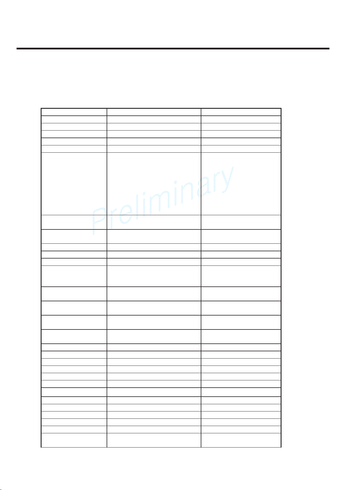
2. PERFORMANCE
2.1 Product Name
BL20 : WCDMA900/2100+EGSM/DCS/PCS
(HSDPA 3.6Mbps / GPRS Class 10 / EDGE Class 10)
2.2 Supporting Standard
Item Feature Comment
Supporting
Standard
Frequency Range WCDMA(FDD1) TX : 1920 – 1980 MHz
Application
Standard
WCDMA(FDD1,8)/EGSM/DCS1800/PCS1900 with
seamless handover
Phase 2+(include AMR)
SIM Toolkit : Class 1, 2, 3, C-E
WCDMA(FDD1) RX : 2110 – 2170 MHz
WCDMA(FDD8) TX : 880 – 915 MHz
WCDMA(FDD8) RX : 925 – 960 MHz
EGSM TX : 880 – 915 MHz
EGSM RX : 925 – 960 MHz
DCS1800 TX : 1710 – 1785 MHz
DCS1800 RX : 1805 – 1880 MHz
PCS1900 TX : 1850 – 1910 MHz
PCS1900 RX : 1930 – 1990 MHz
WAP 2.0, JAVA 2.0
2. PERFORMANCE
2.3 Main Parts : GSM Solution
Item Part Name Comment
Digital Baseband QSC6270 : Qualcomm
Analog Baseband QSC6270 : Qualcomm
RF Chip QSC6270 : Qualcomm
Copyright © 2009 LG Electronics. Inc. All right reserved.
Only for training and service purposes
- 7 -
LGE Internal Use Only

2. PERFORMANCE
2.4 HW Features
Item Feature Comment
Form Factor Slider type
Battery
Size Standard :
Weight 115g With Battery
Volume TBD
PCB LX-BUMP 2 10 Layers
Stand by time 2G Up to 300 hrs
Charging time 4 hrs @ Power Off / 900mAh
Talk time 2G Up to 180mins
RX sensitivity WCDMA(FDD1) : -106.7 dBm
TX output
power
GPRS compatibility GPRS Class 10
EDGE compatibility EDGE Class 10
SIM card type Plug-In SIM
Display 2.4” TFT QVGA
WCDMA/
GSM/
GPRS
EDGE GSM 900 : 27 dBm
1) Capacity
Standard : Li-Ion, 900mAh
2) Packing Type : Soft Pack
106.9 X 50.8 X 12.3mm
3G Up to 300 hrs
3G Up to 110 mins
WCDMA(FDD8) : -103.7 dBm
EGSM : -105 dBm
DCS 1800 : -105 dBm
PCS 1900 : -105 dBm
WCDMA : 24dBm/3.84MHz,+1/-3dBm
EGSM : 33dBm
DCS 1800 : 30 dBm
PCS 1900 : 30 dBm
DCS 1800 : 26 dBm
PCS 1900 : 26 dBm
3V /1.8V
@ Paging Period 5 (2G)
@ DRX 7 (3G)
@ Power Level 5 (2G)
@ Tx = 12dBm (3G)
Class3(WCDMA)
Class4 (EGSM)
Class1 (PCS)
Class1 (DCS)
E2 (GSM900)
E2 (PCS)
E2 (DCS)
Built-in Camera 5M CMOS Camera
Status Indicator Yes
Keypad Function Key : 4
Navigation Key : 5
ANT Main : Internal Fixed Type
System connector 5 Pin
Ear Phone Jack 3.5Phi, 4 Pole, Stereo
PC synchronization Yes
Memory NAND Flash : 2Gbit
SDRAM : 1Gbit
Speech coding FR, EFR, HR,AMR
Data & Fax Built in Data & Fax support
LGE Internal Use Only Copyright © 2009 LG Electronics. Inc. All right reserved.
- 8 -
Navigation Key:
Cancel Key, Menu Key,
Send Key, END/PWR Key
Only for training and service purposes

2. PERFORMANCE
Vibrator Built in Vibrator
Blue Tooth V2.1,A2DP
MIDI(for Buzzer
Function)
Music Player MP3/AAC/AAC+/WMA
Video Player MPEG4, H.263 40fps@QVGA
Camcorder MPEG4, 15fps@QVGA
Voice Recording Yes
Speaker Phone mode
Support
Travel Adapter Yes
CDROM Yes
Stereo Headset Yes
Data Cable Yes
T-Fla sh
(External Memory)
SW Decoded 64Poly
Yes
Yes
Copyright © 2009 LG Electronics. Inc. All right reserved.
Only for training and service purposes
- 9 -
LGE Internal Use Only
2. PERFORMANCE
2.5 SW Features
Item Feature Comment
RSSI 0 ~ 7 Levels
Battery Charging 0 ~ 3 Levels
Key Volume 0 ~ 7 Level
Audio Volume 1 ~ 20 Level
Time / Date Display Yes
Multi-Language Yes (English,German,Dutch,Czech,
Hungarian,Croatian,Polish,
Slovak,Turkish,French,
Italian,Spanish,Swedish,
Danish,Romanian,Greek,
Portuguese,Bulgarian,
TradChinese,SimpChinese,
Russian,Slovenian,Korean,Icela
ndic)
Quick Access Mode Dialing / Call Log / Contact / Menu /
Message / Camera / Favorite
PC Sync Schedule / Phonebook / MEMO /
SMS / Download (Photo, file)
Speed Dial Yes (1~9) Voice mail center -> 1 key
Profile Yes
CLIP / CLIR Yes
Phone Book Name + 5 Numbers + 1 Memo + 2 e-
mail + 3 Group Select + Picture +
Ringtone + Anniversary day
Last Dial Number Yes Total Call DB Max 100
Last Received
Number
Last Missed Number Yes Total Call DB Max 100
Search by Number
/ Name
Group 30
Fixed Dial Number Yes
Service Dial Number Yes
Own Number Yes
Voice Memo Yes
Call Reminder Yes
Network Selection Automatic
Mute Yes
Call Divert Yes
Call Barring Yes
Call Charge (AoC) Yes
Call Duration Yes
SMS (EMS) 1000 EMS : Release4
Yes Total Call DB Max 100
Name and Number
Total 1000 Member
LDN (SIM) N/A
LDN (SIM) N/A
LDN (SIM) N/A
(Except Text align)
LGE Internal Use Only Copyright © 2009 LG Electronics. Inc. All right reserved.
- 10 -
Only for training and service purposes
2. PERFORMANCE
SMS Over GPRS Yes
EMS Melody / Picture
Send / Receive / Save
MMS MPEG4
Send / Receive / Save
Long Message MAX 1000 Characters SMS 7pages
Cell Broadcast Yes
Download Over the WAP
Game Yes
Calendar Yes
Memo 100
World Clock Yes
Unit Convert Currency/Surface/Length/Volume/W
Stop Watch Yes
Wall Paper Yes
WAP Browser Over WAP 2.0 Obigo
Download Melody /
Wallpaper
SIM Lock Yes Operator Dependent
SIM Toolkit Yes R99
MMS Yes Obigo +LG MMS Client
EONS No
CPHS Yes V4.2
ENS No
Camera Yes 5M AF /
JAVA Yes CLDC V1.1 / MIDP V2.1
Voice Dial No
IrDa No
Bluetooth Yes BT 2.1+EDR
FM radio Yes
Ye s
Receive only
Ye s
Ye s
eight/Temperature/Velocity
Yes Over WAP
Digital Zoom : x2
Download Over WAP
HFP/HSP/A2DP&AVRCP
/OPP/BPP/PBAP/SPP/DUN/FTP
GPRS Yes Class 12
EDGE Yes Class 12
Hold / Retrieve Yes
Conference Call Yes Max. 6
DTMF Yes
Memo pad Yes
TTY No
AMR Yes
SyncML Yes
IM Yes(Only Orange) ORANGE MSN
Email Yes
Copyright © 2009 LG Electronics. Inc. All right reserved.
Only for training and service purposes
- 11 -
LGE Internal Use Only
2. PERFORMANCE
T
2.6 HW SPEC.
1) GSM transceiver specification
Item Specification
Phase Error
Frequency Error
EMC(Radiated Spurious Emission
Disturbance)
ransmitter Output power and Burst
Timing
Burst Timing <3.69us
Spectrum due to modulation out to
less than 1800kHz offset
Spectrum due to modulation out to
larger than 1800kHz offset to the
edge of the transmit band
Spectrum due to switching transient
Reference Sensitivity – TCH/FS Class II(RBER) : -105dBm(2.439%)
Usable receiver input level range 0.012(-15 - -40dBm)
Intermodulation rejection – Speech
channels
Rms : 5°
Peak : 20 °
GSM : 0.1 ppm
DCS/PCS : 0.1 ppm
GSM/DCS : < -28dBm
GSM : 5dBm – 33dBm ± 3dB
DCS/PCS : 0dBm – 30dBm ± 3dB
200kHz : -36dBm
600kHz : -51dBm/-56dBm
GSM :
1800-3000kHz :< -63dBc(-46dBm)
3000kHz-6000kHz : <-65dBc(-46dBm)
6000kHz < : < -71dBc(-46dBm)
DCS :
1800-3000kHz :< -65dBc(-51dBm)
6000kHz < : < -73dBc(-51dBm)
400kHz : -19dBm/-22dBm(5/0), -23dBm
600kHz : -21dBm/-24dBm(5/0), -26dBm
± 800kHz, ± 1600kHz
: -98dBm/-96dBm (2.439%)
AM Suppression
GSM : -31dBm
- DCS : -29dBm
Timing Advance ± 0.5T
-98dBm/-96dBm (2.439%)
LGE Internal Use Only Copyright © 2009 LG Electronics. Inc. All right reserved.
- 12 -
Only for training and service purposes
2) WCDMA transmitter specification
Item Specification
Transmit Frequency Band1 : 1920 MHz ~ 1980 MHz
Band8 : 880MHz~915MHz
Maximum Output Power +24 dBm / 3.84 MHz, +1 / -3 dB
Frequency Error within ±0.1 PPM
Open Loop Power Control Normal Conditions : within ±9 dB,
Extreme Conditions : within ±12 dB
Minimum Transmit Power < -50 dBm /3.84 MHz
Occupied Bandwidth < 5 MHz at 3.84 Mcps (99% of power)
Adjacent Channel Leakage
Power Ratio (ACLR)
Spurious Emissions
|f-fc| > 12.5 MHz
> 33 dB @ ±5 MHz,
> 43 dB @ ±10 MHz
< -36 dBm / 1 kHz RW @ 9 kHz ≤ f < 150 kHz
< -36 dBm / 10 kHz RW @ 150 KHz ≤ f < 30 MHz
< -36 dBm / 100 kHz RW @ 30 MHz ≤ f < 1 GHz
< -30 dBm / 1 MHz RW @ 1 GHz ≤ f < 12.75 GHz
< -60 dBm / 3.84 MHz RW @ 869 MHz ≤ f ≤ 894 MHz
< -60 dBm / 3.84 MHz RW @ 1930 MHz ≤ f ≤ 1900 MHz
< -60 dBm / 3.84 MHz RW @ 2110 MHz ≤ f ≤ 2155 MHz
< -67 dBm / 100 kHz RW @ 925 MHz ≤ f ≤ 935 MHz
< -79 dBm / 100 kHz RW @ 935 MHz < f ≤ 960 GHz
< -71 dBm / 100 kHz RW @ 1805 MHz ≤ f ≤ 1880 MHz
< -41 dBm / 300 kHz RW @ 1884.5 MHz < f < 1919.6 MHz
Transmit Intermodulation < -31 dBc @ 5 MHz & < -41 dBc @ 10 MHz
when Interference CW Signal Level = -40 dBc
Error Vector Magnitude < 17.5 %, when Pout ≥ -20 dBm
Peak Code Domain Error
< -15 dB at Pout t -20 dBm
2. PERFORMANCE
Copyright © 2009 LG Electronics. Inc. All right reserved.
Only for training and service purposes
- 13 -
LGE Internal Use Only
2. PERFORMANCE
3) WCDMA receiver specification
Item Specification
Receive Frequency Band1 : 2110 ~ 2170 MHz
Band8 : 925~960MHz
Reference Sensitivity Level Band1 : BER < 0.001 when Îor = -106.7 dBm / 3.84 MHz
Band8 : BER < 0.001 when Îor = -103.7 dBm / 3.84 MHz
Maximum Input Level BER < 0.001 when Îor = -25 dBm / 3.84 MHz
Adjacent Channel Selectivity
(ACS)
Blocking Characteristic BER < 0.001 when Îor = -103.7 dBm / 3.84 MHz
Spurious Response BER < 0.001 when Îor = -103.7 dBm / 3.84 MHz
Intermodulation BER < 0.001 when Îor= -103.7 dBm / 3.84 MHz
Spurious Emissions < -57 dBm / 100 kHz BW @ 9 kHz ≤ f < 1 GHz
ACS > 33 dB where BER < 0.001 when
Îor = -92.7 dBm / 3.84 MHz
& Ioac = –52 dBm / 3.84 MHz @ ±5 MHz
& Iblocking = -56 dBm / 3.84 MHz @ Fuw(offset) = ±10 MHz
or Iblocking = -44 dBm / 3.84 MHz @ Fuw(offset) = ±15 MHz
& Iblocking = -44 dBm
& Iouw1 = -46 dBm @ Fuw1(offset) = ±10 MHz
& Iouw2 = -46 dBm / 3.84 MHz @ Fuw2(offset) = ±20 MHz
< -47 dBm / 1 MHz BW @ 1 GHz ≤ f ≤ 12.75 GHz
Inner Loop Power Control
In Uplink
Adjust output(TPC command)
cmd 1dB 2dB 3dB
+1 +0.5/1.5 +1/3 +1.5/4
0 -0.5/+0.5 -0.5/+0.5 -0.5/+0.5
-1 -0.5/-1.5 -1/-3 -1.5/-4
group(10equal command group)
+1 +8/+12 +16/+24
LGE Internal Use Only Copyright © 2009 LG Electronics. Inc. All right reserved.
- 14 -
Only for training and service purposes
4) HSDPA transmitter specification
Item Specification
Transmit Frequency Band1 : 1920 MHz ~ 1980 MHz
Band8 : 880MHz~915 MHz
Maximum Output Power Sub-Test
1=1/15, 2=12/15 21~25dBm / 3.84 MHz
3=13/15 4=15/8 20~25dBm / 3.84 MHz
5=15/7 6=15/0 19~25dBm / 3.84 MHz
Sub-test
in table
C.10.1.4
HS-DPCCH
Power
5
Power step slot
step
1 Start of
2 Start of CQI 1 +/- 0.6
3 Middle of CQI 0 +/- 0.6
boundary
Ack/Nack
2. PERFORMANCE
Power
step size,
P [dB]
6 +/- 2.3
Transmitter power
step tolerance [dB]
Sub-Test : 1=1/15, 2=12/15, 3=13/15, 4=15/8, 5=15/7, 6=15/0
Frequency offset
Spectrum Emission Mask
Adjacent Channel Leakage
Power Ratio (ACLR)
Error Vector Magnitude < 17.5 %, when Pout ≥ -20 dBm
5) HSDPA receiver specification
Item Specification
Receive Frequency
Maximum Input Level
(BLER or R), 16QAM Only
from carrier f
2.5 ~ 3.5 MHz
3.5 ~ 7.5 MHz
7.5 ~ 8.5 MHz
8.5 ~ 12.5 MHz -49dBc 1 MHz
Sub-Test : 1=1/15, 2=12/15, 3=13/15, 4=15/8, 5=15/7, 6=15/0
> 33 dB @ ±5 MHz
> 43 dB @ ±10 MHz
Band1 : 2110 ~ 2170 MHz
Band8 : 925 ~ 960Hz
Sub-Test : 1=1/15, 2=12/15, 3=13/15, 4=15/8, 5=15/7, 6=15/0
BLER < 10% or R >= 700kbps
Minimum requirement
-35-15×(f-2.5)dBc
-35-1×(f-3.5)dBc
-35-10×(f-7.5)dBc
Measurement
Bandwidth
30 kHz
1 MHz
1 MHz
Copyright © 2009 LG Electronics. Inc. All right reserved.
Only for training and service purposes
- 15 -
LGE Internal Use Only
3. Technical Brief
3. TECHNICAL BRIEF
3.1 GENERAL DESCRIPTION
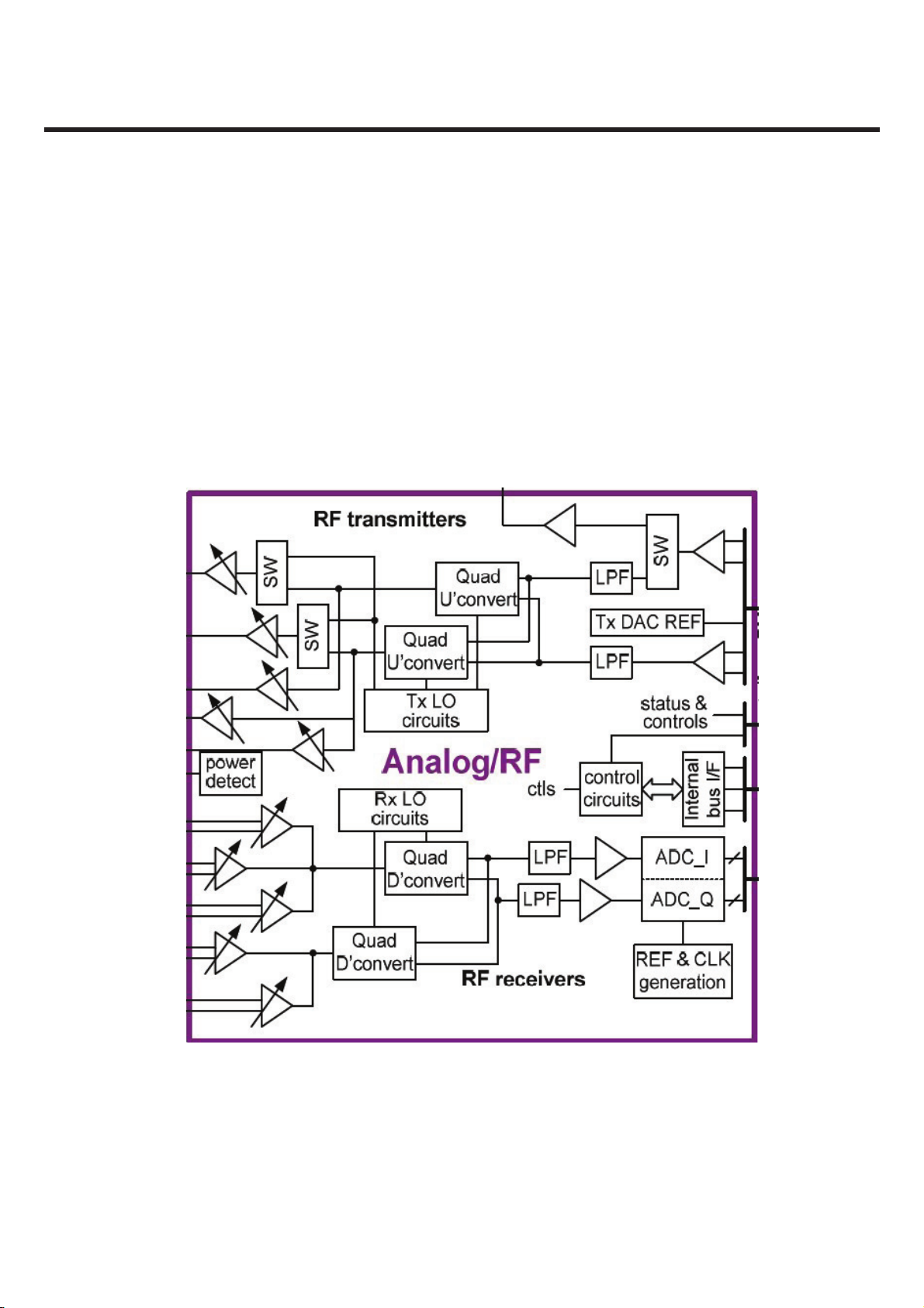
The RF platform of BL20 supports two different communication modes (WCDMA/GSM modes) including five
communication bands (W2100/W850/GSM900/GSM1800/GSM190). The all the RF blocks can be divided into
three main parts, which are a WCDMA part, a GSM, and an antenna switch Mode.
The simplifed block diagram is shown in Figure 1.1.1i
[Figure 1-1] Block diagram of RF part
LGE Internal Use Only Copyright © 2009 LG Electronics. Inc. All right reserved.
- 16 -
Only for training and service purposes

3. Technical Brief
3.2 GSM MODE
The EDGE/GPRS/GSM transceiver use a digital interface that is shared between receive and transmit data.
The receive interface is based on I and Q data and the transmitter interface is based on envelop and
frequency data.
The quad band EDGE/GSM/GPRS transceiver has the following general features:
Power class
GMSK low bands: Class 4 (33 dBm)
GMSK high bands: Class 1 (30 dBm)
8PSK low bands: Class E2 (27 dBm)
8PSK high bands: Class E2 (26 dBm)
Multi slot class 12 (4+4=5)
Dual Transfer Mode (DTM) class 9 (3+2=5)
Zero-IF receiver
-Polar modulation transmitter
3.2.1 GSM RECEIVER
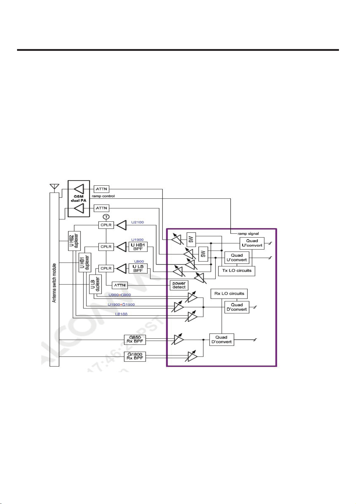
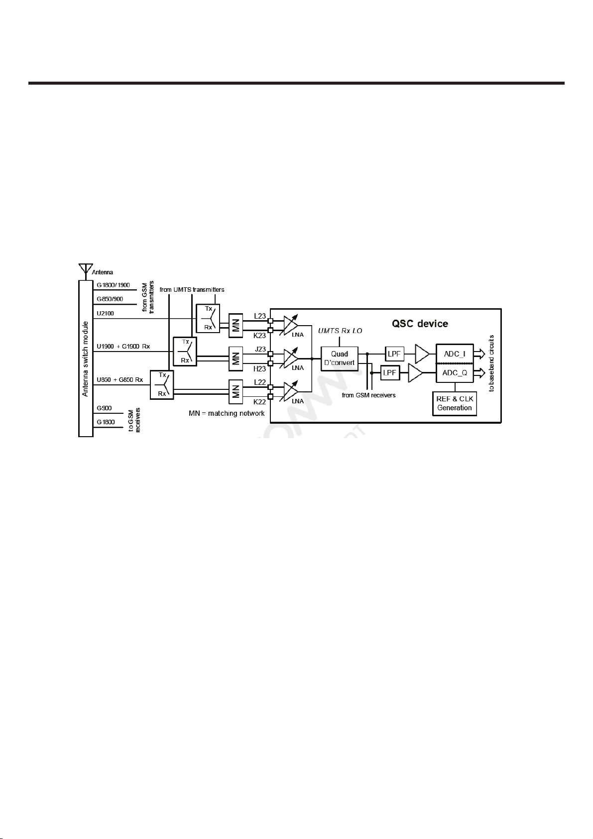
There are two recommended GSM receiver path configurations; bothare shown in Figure 1.3.2.1. The
configuration shown on top allows the GSM 850 and GSM 1900 bands to share the UMTS 850 and UMTS 1900
paths for US applications and uses four LNA inputs to support quad-band GSM operation.
The lower example uses two LNAsfor quad-band GSM operation (one low band and one high
band), with two-way SAW filters between the antenna switch and the QSC inputs for each
band type.
Copyright © 2009 LG Electronics. Inc. All right reserved.
Only for training and service purposes
- 17 -
LGE Internal Use Only
3. Technical Brief
[Figure 1-2] QSC GSM receiver signal paths functional diagram
LGE Internal Use Only Copyright © 2009 LG Electronics. Inc. All right reserved.
- 18 -
Only for training and service purposes

3. Technical Brief
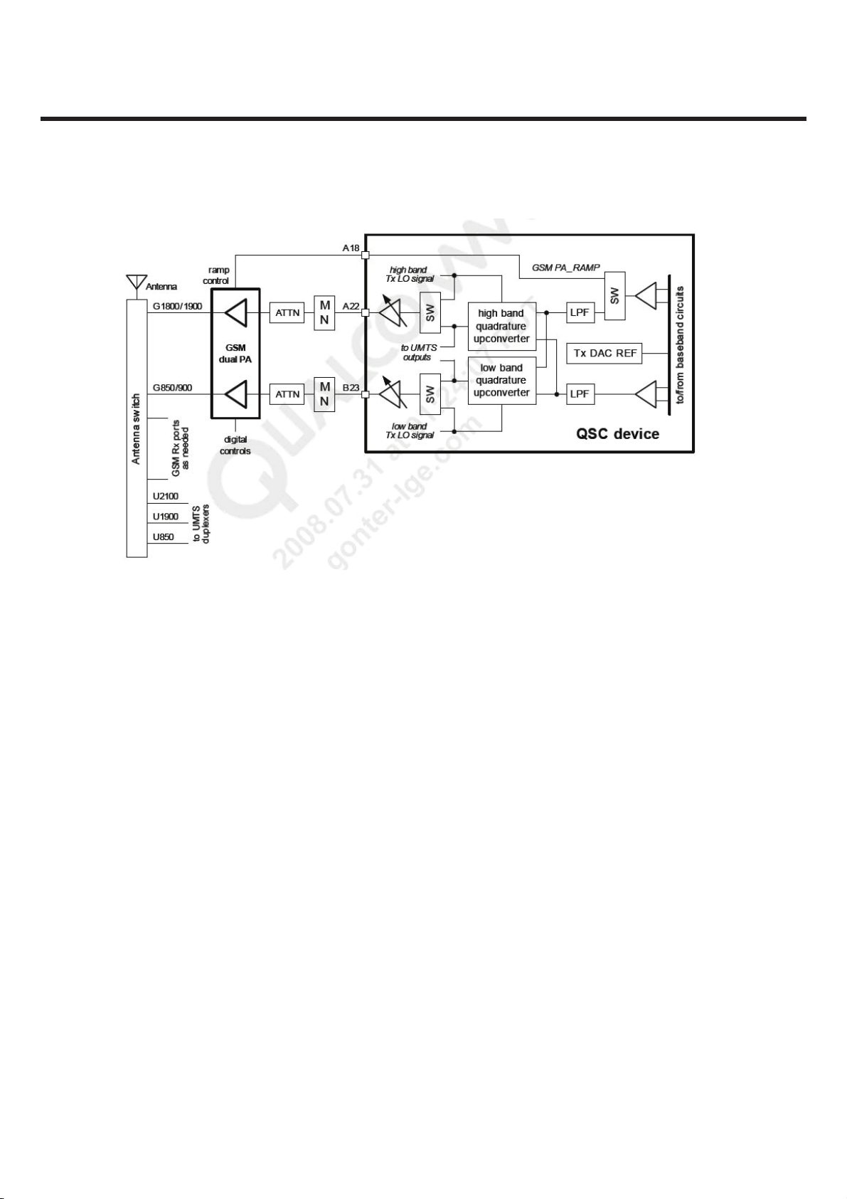
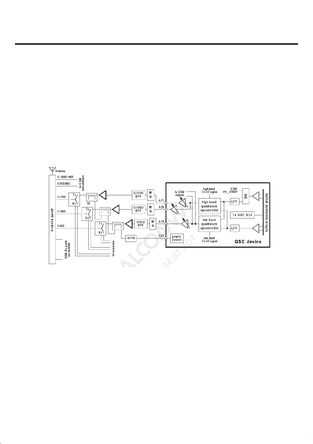
3.2.2 GSM TRANSMITTER
The QSC62x0 device supports quad-band GSM transmissions with two separate dual-band
driver amplifer outputs; in fact, most Tx active circuits are contained within the device.
Both GSM transmit paths (Figure 1.3.1.1) begin with a single, shared analog baseband
signal from the device’s baseband circuits - the same interface and baseband circuits used
by the UMTS transmitters. The GSM transmitters use the same quadrature upconvertersas well
- one for low band signals and one for high band —with just one active at a time. The
transmiter LO signals are generated by circuits described.
in next section and delivered to the upconvertercircuits at the correct frequency, with
the proper phase relationship, and with an adequate drive level.
The SPDT switches at each driver amplifier input allow selectionof the output signal:
either the actual GSM signal from the upconverteror a test signal generated by the Tx LO
synthesizer. The Tx output chain is functionally identical for both the low band and the
high band: the power amplifer is driven by the QSC device through a matching network
and a resistive attenuator; the PA output is routed to the antenna switch module whose
output is connected to the antenna. In addition to the through signal path, the QSC device
also provides the PA ramp control signal that ensures smooth transitions while the
transmitter is turned on and off for GSM’sburst transmissions.
The ramp signal is generated by one of the baseband circuit’s Tx DACs. A switch after
the baseband amplifer selects whether the DAC output signal is routed to GSM PA
module for ramping the PA up or down, or to the transmitter signal path fo
transmission.
Copyright © 2009 LG Electronics. Inc. All right reserved.
Only for training and service purposes
- 19 -
LGE Internal Use Only
3. Technical Brief
[Figure 1.2.2] QSC GSM transmitter signal paths functional diagram
LGE Internal Use Only Copyright © 2009 LG Electronics. Inc. All right reserved.
- 20 -
Only for training and service purposes
3. Technical Brief
3.3 UMTS MODE
The W-CDMA transceiver uses differential analog in-phase and quadrature-phase interfaces,
That is an IQ-interface, both in the receiver and transmitter information path..
The transceiver has the following general features:
. Power class : Power class 3 (+24dBm) in Band II and V
. Zero-IF Receiver.NoIF filter needed
. Direct IQ modulation transmitter
[Figure 1.3.1] WCDMA RF structure
Copyright © 2009 LG Electronics. Inc. All right reserved.
Only for training and service purposes
- 21 -
LGE Internal Use Only
3. Technical Brief
3.3.1 UMTS RECEIVER
The antenna collects the base station forward-link signal and radiates the phone’s reverse-link signal. In the
example of a multiband, multimode phone (Figure 1.2.2.1), a switch routes the antenna signals to one of the
three UMTS Rx/Tx paths, each begining with its own band-specific duplexer that separates that band’s receive
and transmit paths
[Figure 1.3.2] WCDMA Receiver schematic
Each UMTS duplexer provides a differential output signal that is comlatible with its QSC LNA input. The
duplexer-to-LNA interface requires a differential matching network (MN) thatoptimizes the power transfer
into the LNA. Although there are three UMTS LNAs, only one is active at a time. The active gain-stepped LNA
output drives a shared quadrature
Downconverter directly —an off-chip inter-stage filter is not required. The elimination of this filter is achieved
by a combination of factors:
-New on-chip QSC processing
-Higher performance achieved by the differential duplexer-to-LNA interface
-Greater duplexer suppression of Tx leakage
The downconverter’sRF circuitry includes another gain-stepped amplifier that supplements the LNA gain
steps to further extend the receiver dynamic range. The downconvertertranslates the active LNA’sRF signal
directly to baseband, producing two analog outputs: in-phase (I) and quadrature (Q). The UMTS baseband
signals are routed to lowpassfilters whose passbandand stopbandcharacteristics are optimized for the active
WCDMA waveform. Both filter outputs are buffered to drive their analog-to-digital converters for digitization.
The digital baseband outputs are routed to QSC baseband circuits for further processing.
LGE Internal Use Only Copyright © 2009 LG Electronics. Inc. All right reserved.
- 22 -
Only for training and service purposes
3. Technical Brief
3.3.2 UMTS TRANSMITTER
The QSC62x0 device support tri-band UMTS transmissions with three separate driver amplifier outputs; in
fact, most Tx active circuits are contained within the device. All three UMTS transmit paths (Figure 1.2.1.1)
begin with a single,shared analog baseband signal from the device’s baseband circuits. The baseband signal
is composed of two differential lines, one in-phase component and one quadrature-phase component. Each
component is lowpassfiltered and amplified to levels sufficient for driving the quadrature upconverters.
There are two upconverters—one for low-band signals and one for high band —but only one upconverteris
active at a time.
[Figure 1.3.3] WCDMA Transceiver Architecture
Each UMTS duplexer provides a differential output signal that is compatible with its QSC LNA input. The
duplexer-to-LNA interface requires a differential matching network (MN) thatoptimizes the power transfer
into the LNA. Although there are three UMTS LNAs, only one is active at a time. The active gain-stepped LNA
output drives a shared quadrature downconverterdirectly - an off-chip inter-stage filter is not required. The
elimination of this filter is achieved by a combination of factors:
-New on-chip QSC processing
-Higher performance achieved by the differential duplexer-to-LNA interface
-Greater duplexer suppression of Tx leakage. The downconverter’sRF circuitry includes another gain-stepped
amplifier that supplements the LNA gain steps to further extend the receiver dynamic range.
The downconvertertranslates the active LNA’sRF signal directly to baseband, producing two analog outputs:
in-phase (I) and quadrature (Q).
Copyright © 2009 LG Electronics. Inc. All right reserved.
Only for training and service purposes
- 23 -
LGE Internal Use Only

3. Technical Brief
The UMTS baseband signals are routed to lowpassfilters whose passbandand stopbandcharacteristics are
optimized for the active WCDMA waveform. Both filter outputs are buffered to drive their analog-to-digital
converters for digitization. The digital baseband outputs are routed to QSC baseband circuits for further
processing.
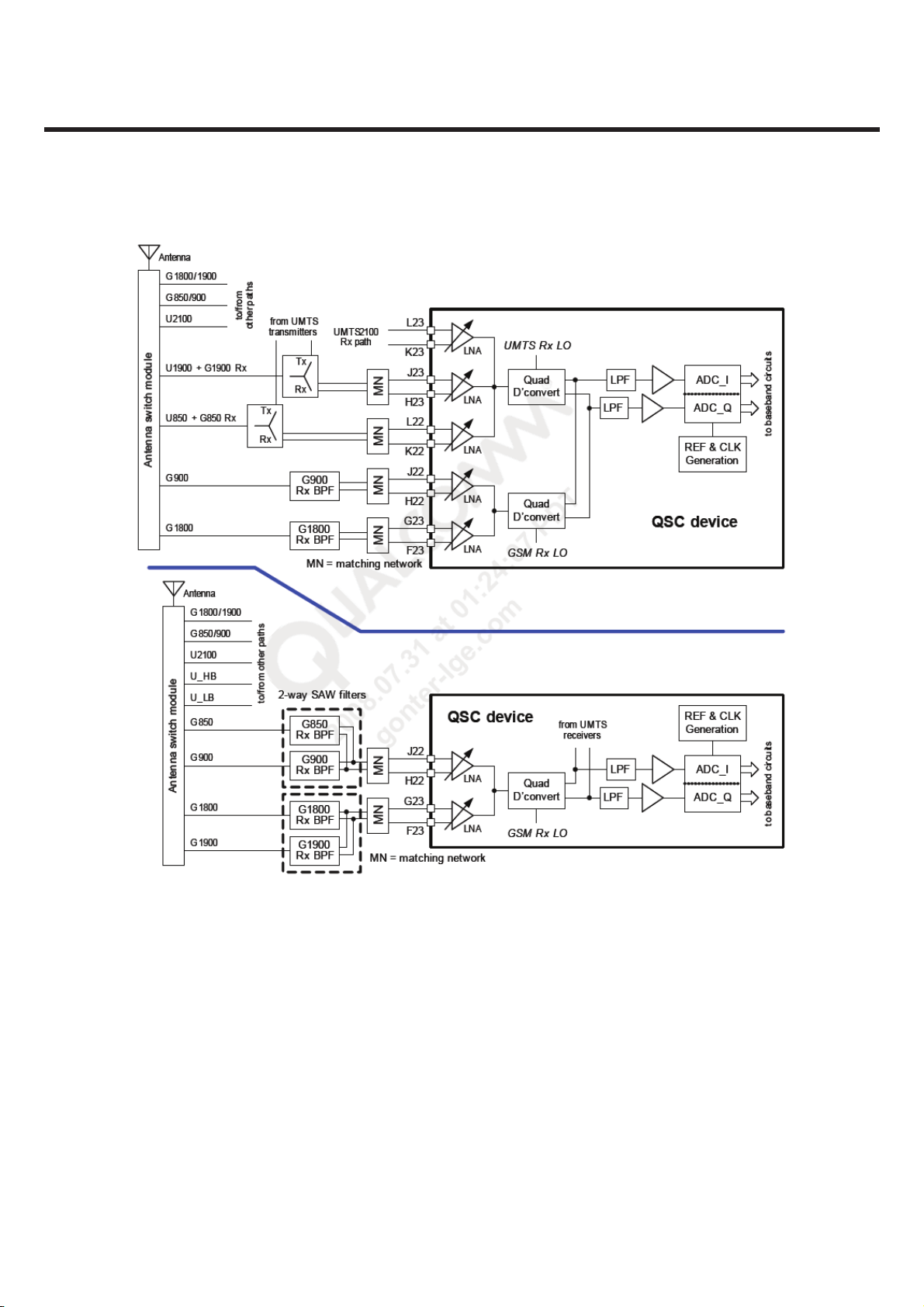
z Shared UMTS/GSM configuration (four GSM LNAs)
In this configuration, the GSM 850 receive path shares the UMTS 850 receiver front-end path (including
LNA).Begining at the antenna switch output, the GSM signal is routedthrough the UMTS850 duplexer to the
shared LNA input at pins L22 and K2. Likewise, the GSM 1900 receive path shares the UMTS 190front-end,
including pins J23 and H23. The GSM 900 and GSM 180bands have dedicated receive paths from the antenna
switch outputs to the QSC LNA inputs.Each band has its own band-select filter that drives its LNA input. All
four GSM bands include input filtering: the 850 and 1900 bands share the UMTS duplexer filtering, while the
900 and 1800 bands have dedicated bandpassfilters. The filter functions suppress out-of-band received
signals and the handset’s GSM transmitter leakage. Transmit power suppression must be adequate to avoid
overdrivingthe GSM Rx chain. Like the UMTS paths,
the GSM paths use a differential configuration into their LNAs, and thus equiredifferential matching networks.
The internal GSM receivers are functionally identical to the UMTS receivers: although there are multiple GSM
LNAs, only one is active at a time. The active gain-stepped LNA output drives a shared quadrature
downconverterdirectly
—an off-chip inter-stage filter is not required. The elimination of this filter is achieved by a combination of
factors:
New on-chip QSC processing
Higher performance achieved by the differential duplexer-to-LNA interface
Greater duplexer suppression of Tx leakage
The downconverter’s RF circuitry includes another gain-stepped amplifier that supplements the LNA gain
step to further extend the receiver dynamic range. The downconvertertranslates the active LNA’sRF signal
directly to baseband, producing two analog outputs: in-phase (I) and quadrature (Q). The GSM baseband
signals drive lowpass filters whose passbandand stopbandcharacteristics are optimized for the active GSM
waveform. Both filter outputs are buffered to drive their analog-to-digital converters for digitization. The
digital baseband outputs are routed to QSC baseband circuits for further processing.The Rx LO signal is
delivered to the downconvertercircuits from the LO generation and distribution circuits as described in next
section.
LGE Internal Use Only Copyright © 2009 LG Electronics. Inc. All right reserved.
- 24 -
Only for training and service purposes

3. Technical Brief
z Dedicated GSM configuration (two GSM LNAs)
In this configuration, the GSM 850 and GSM 1900 bands do not pass through the UMTS duplexers.
Instead, the two GSM LNA inputs are shared: the GSM 850 and GSM 900 bands share the low-band GSM LNA,
and the GSM 180and GSM 190bands share the high-band LNA. Four switch module outputs are required,
each driving its own GSM Rx path. A two-way SAW filter takes the two low-band (or high-band) single-ended
inputs from the antenna switch and provides one filtered, differential output that drives the appropriate QSC
LNA input.
Beyond the LNA inputs, this GSM receiver configuration is identical to the paths described earlier for the
shared UMTS/GSM configuration.
3.3.3. Rx LO circuits
The QSC62x0 device integrates all of the frequency synthesizer functions that generate the UMTS and GSM
receive LO signals (UHF local oscillator, PLL circuits, and loop filter), plus the distribution circuits that deliver
the quadrature LO signals to the two downconverters.
The buffered 19.2 MHz TCXO or XO signal provides the synthesizerinput (REF), the frequency refrence to
which the PLL is phase and frequency locked. The refernce is divided to create a fixed frequency input to the
phase detector, FR. The other phase detector input (FV) varies as the loop acquires a lock and is generated by
dividing the local oscillator output frequency using the feedback path’s counter. The closed-lop wilforce FV to
equal FR when locked.
If the loop is not locked, the error between FV and FR will create an error signal. This error signal is filtered by
the loop filter and applied to the local oscillator, tuning the output frequency so that the error is decreased.
Ultimately the loop forces the error to approach zero and the PLL is phase and frequency locked.
Copyright © 2009 LG Electronics. Inc. All right reserved.
Only for training and service purposes
- 25 -
LGE Internal Use Only
3. Technical Brief
3.4 OFF-CHIP RF COMPONENTS
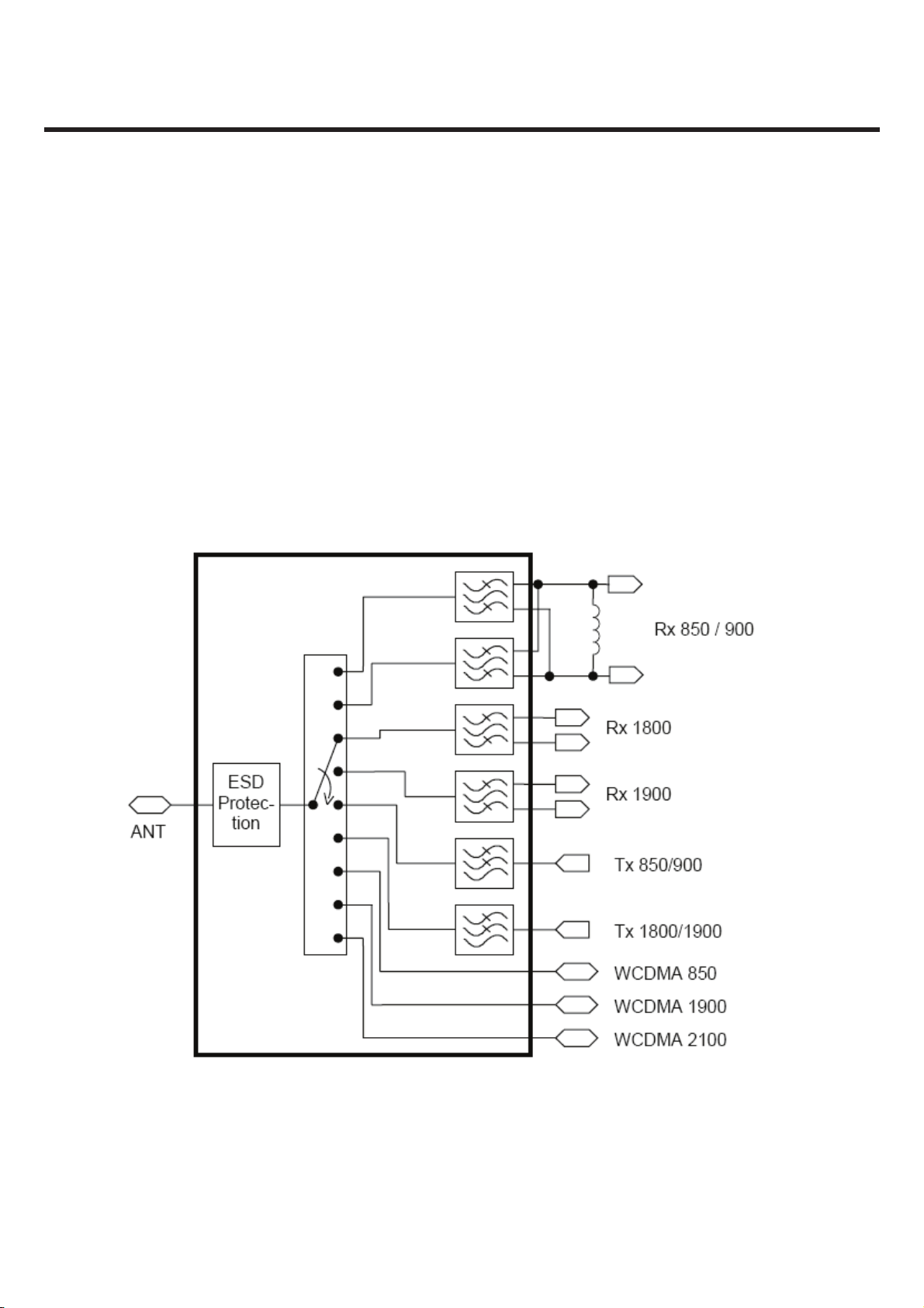
3.4.1 LMSP43QL-873 (FL100: FEM)
■Low-loss SAW frontend module for mobile telephone systems e
■Covering GSM850, GSM900, GSM1800, GSM1900, WCDMA 2100bands
■Integration of TX low pass filters, switches and decoder
■Integration of GSM 850, EGSM, PCN and PCS RX SAWs
■Balanced outputs of all RX ports, diplexed for GSM 850/ EGSMa
■Integration of ESD protection at Ant port to 8kV
acc. IEC-61000-4-2 (contact discharge)
[Figure 1.4.1] Block diagram of FEM
LGE Internal Use Only Copyright © 2009 LG Electronics. Inc. All right reserved.
- 26 -
Only for training and service purposes
3. Technical Brief
p
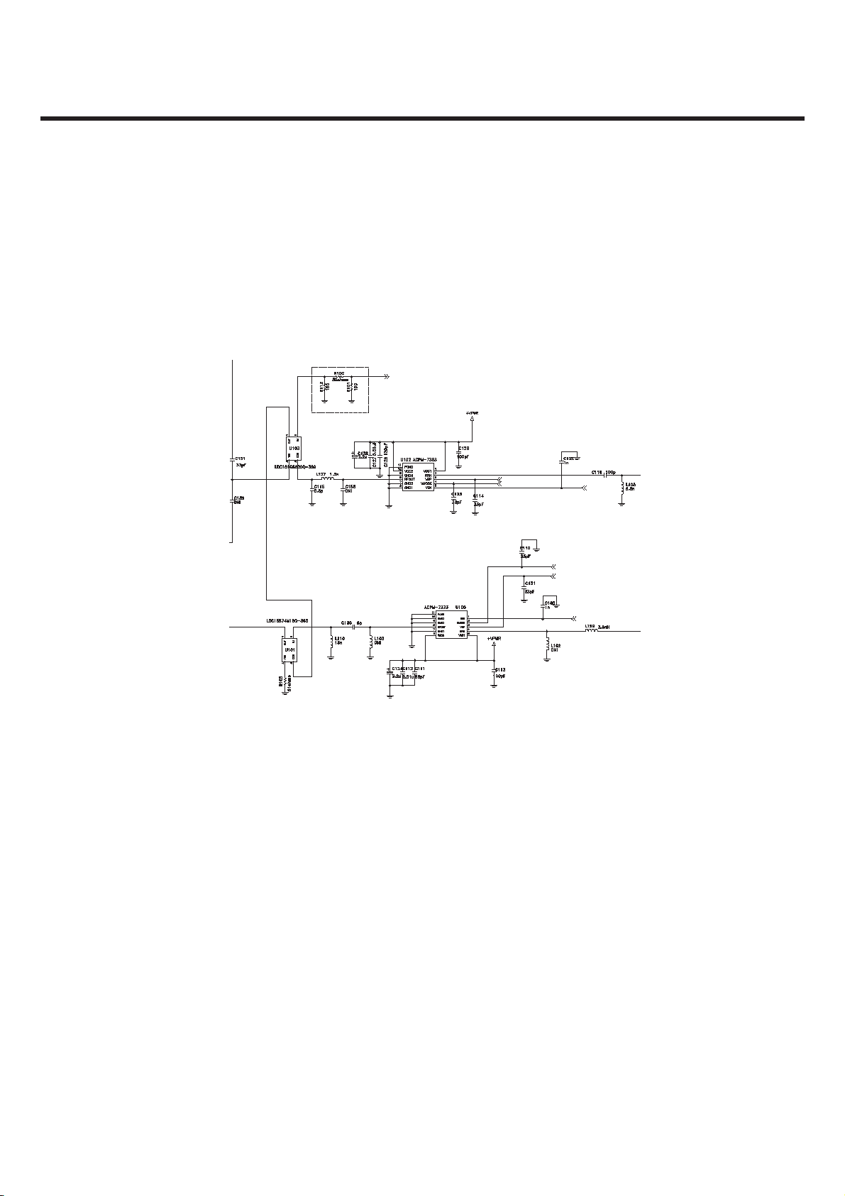
3.4.2 W-CDMA Power Amplifier (U102/104:
ACPM7383/7311) and Coupler(U101/103: LDC151G8620Q-359/LDC15874M19Q-360)
The UMTS PA output power is monitored by external power detector circuits(Coupler : and HDET function in
QSC6270). This detector voltage can be used for transmitter calibration and monitor to meet RF system
specification.
6dB Atten
F, when W1900 enabled
L127= 1nH, when W1900 enabled
PWR_DET
PA_R1
PA_R0
WCDMA_PA_ON0
PA_R0
PA_R1
WCDMA_PA_ON1
C130= 100pF, when W850 enabled
L110= DNI, when W850 enabled
[Figure 1.4.2] W-CDMA PAM, HDET, and Duplexer circuits.
Copyright © 2009 LG Electronics. Inc. All right reserved.
Only for training and service purposes
- 27 -
LGE Internal Use Only
3. Technical Brief
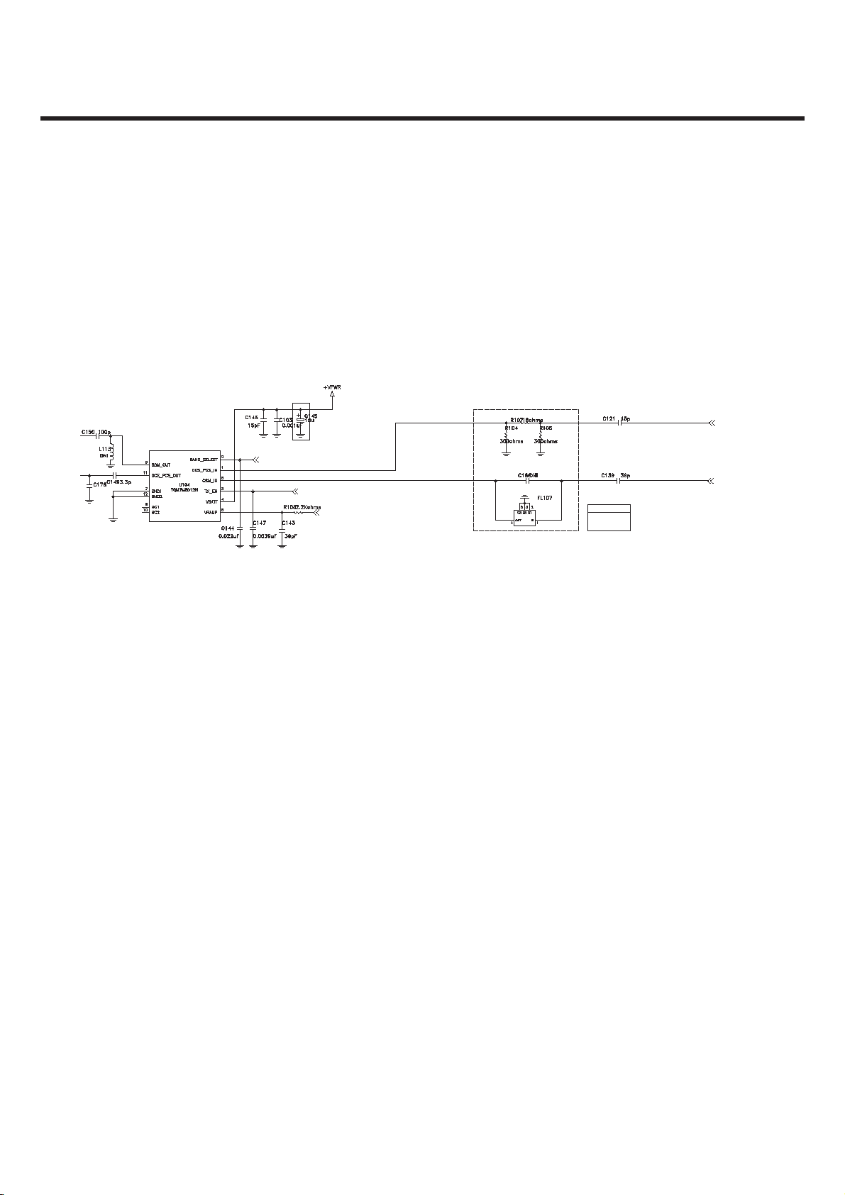
3.4.3 GSM850/EGSM/DCS/PCS Dual band Transmit Power Amplifier
(U101: TQM7M5012)
The dual band PA is operating to transmit for low band (GSM-850, GSM-900) and high band (GSM-1800,
GSM1900). Operating mode is selected and controlled by the QSC6270.(GSM_PA_BAND)
TX_GSM_HB
GSM_PA_BAND
DNI
GSM_PA_EN
GSM_PA_RAMP
GSM TX
3dB
B9442
3dB
EGSM Tx
SFSY0037601
B9442
TX_GSM_LB
[Figure 1.4.3] GSM900 /DCS/PCS TX Power Amplifier path
LGE Internal Use Only Copyright © 2009 LG Electronics. Inc. All right reserved.
- 28 -
Only for training and service purposes
3.5 OFF-CHIP COMPONENTS
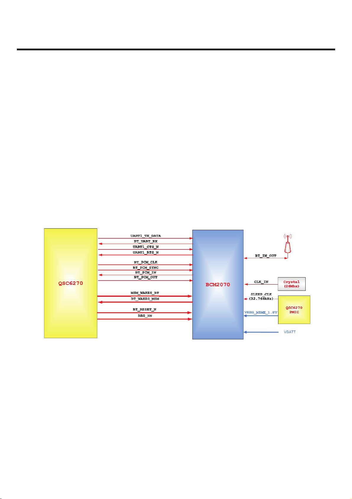
3.5.1 Bluetooth (BCM2070)
3. Technical Brief
Bluetooth block of BL20 consists of a BCM2070 chip-set, an external crystal oscillator(26MHz), and a
Bluetooth chip antenna (2.4GHz). QSC6270, which is main HW solution of BL20 Model, doesn’t include BT
baseband core. Instead, Bluetooth chipset, BCM2070, contains stand-alone baseband processor (V2.1+EDR)
as well as BT RF block. An external crystal oscillator (26MHz) is used to provide reference frequency to
BCM2070.
Figure 1 shows the Bluetooth system architecture in the BL20.
[Figure 1.5] Bluetooth system architecture
Copyright © 2009 LG Electronics. Inc. All right reserved.
Only for training and service purposes
- 29 -
LGE Internal Use Only
3. Technical Brief
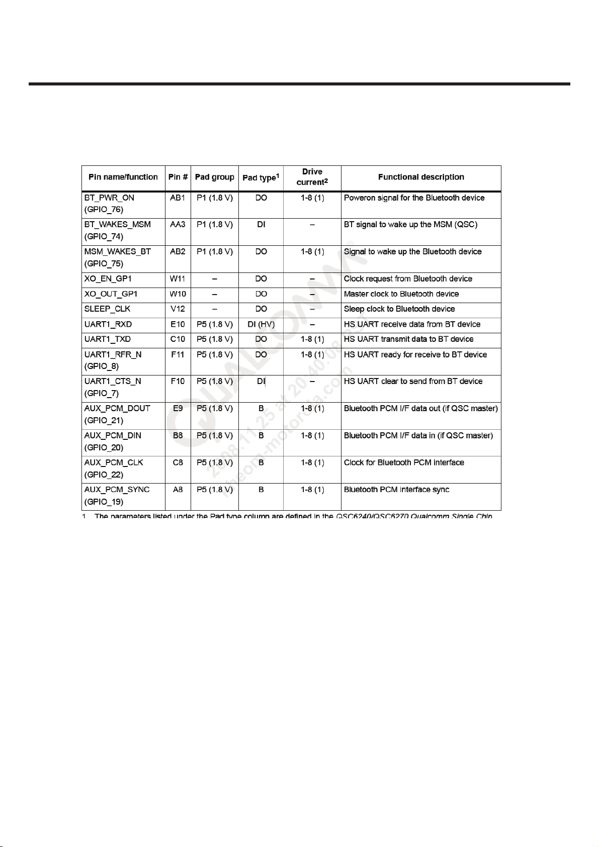
Table 1. Bluetooth Connection(GPIO) with QSC6270
LGE Internal Use Only Copyright © 2009 LG Electronics. Inc. All right reserved.
- 30 -
Only for training and service purposes
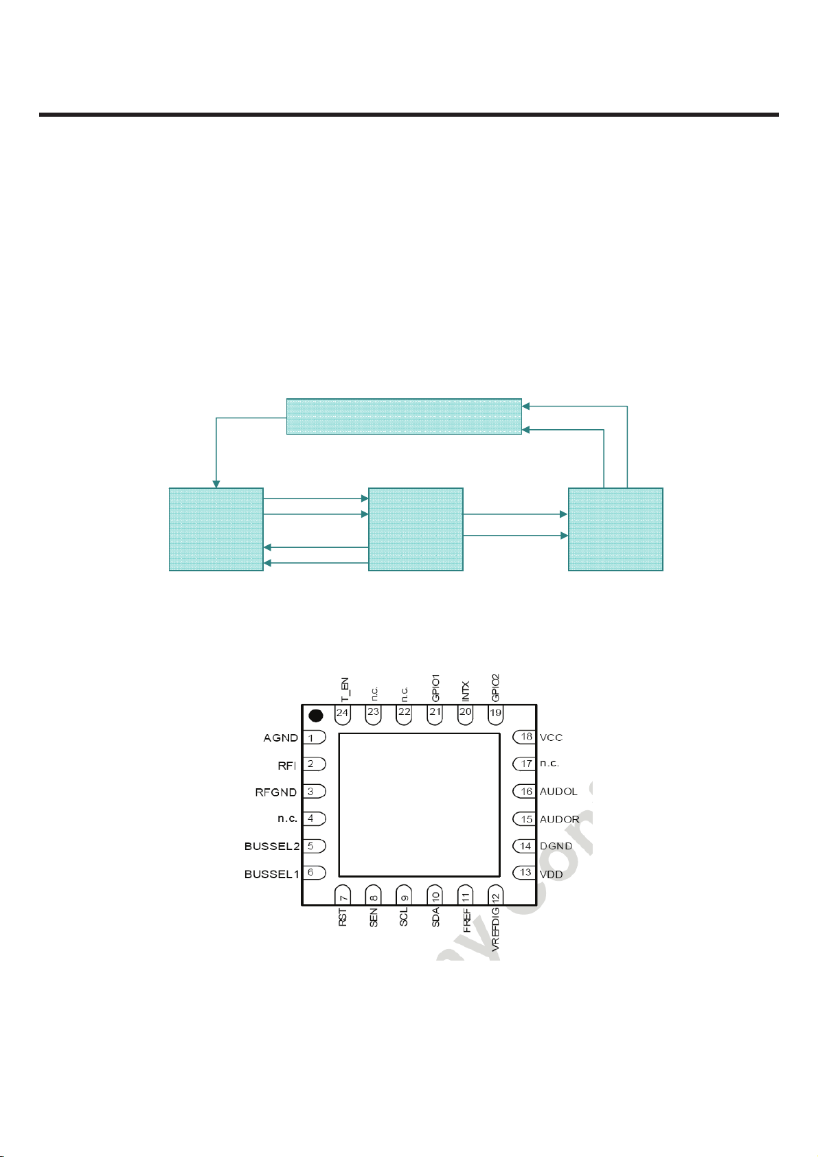
3.5.2 FM Receiver (TEA5991)
3. Technical Brief
The TEA5991 is a single chip FM stereo radio with RDS and RBDS decoder. The radio can be connected to a
headphone antenna and can tune from 70-108 MHz to cover the European, US, Chinese and Japanese FM
band. The radio delivers stereo audio output to an external amplifier. The radio can be controlled with a high
level command based interface through a I2C or SPI-bus.
[Figure3.xx.x.x] shows the FM Radio system architecture in the BL20.
5pin MicroUSB Connector
FM_ANT
FM
TEA5991
FM_R
FM_L
FM_I2C_SDA
FM_I2C_SDL
QSC6270
[Figure3.xx.x.x]
HP_R
HP_L
HP_EAR_R
HP_EAR_L
AUDIO
SUBSYSTEM
Pin Descriptions
Copyright © 2009 LG Electronics. Inc. All right reserved.
Only for training and service purposes
[Figure3.xx.x.x]
- 31 -
LGE Internal Use Only
 Loading...