

Page 1

B1300
SERVICE MANUAL
SERVICE MANUAL
Page 2

Table of Contents
Chapter 1 - Performance
1-1. Performance …………………………………………..
1-2. HW Feature ……………………………………………
Chapter 2 – Technical Brief
2-1. The RF Chipset ………………………………………
2-2. The PA Circuit ……………………………………….
2-3. Peripheral Circuit ……………………………………
2-4. Digital Baseband Chip ………………………………
2-5. Analog Baseband Chip ………………………………
2-6. CPU Memories ……………………………………….
2-7. Power Supplies ……………………………………….
2-8. Battery Charge Interface ………………………….
2-9. System Connector ………………………………….
2-10. Keypad Switches and Scanning …………………..
2-11. Display Interface …………………………………….
2-12. Microphone …………………………………………..
2-13. Receiver/Speaker/Buzzer …………………………
2-14. Headset Interface …………………………………..
2-15. Back-light Illumination ……………………………
2-16. Vibrator ………………………………………………
……………………
……………………
4
4
10
11
11
15
16
16
18
20
20
22
24
26
27
28
28
29
29
29
Chapter 3 – Failure List
Chapter 4 – Trouble Shooting
4-1. Power Supply …………………………………………
4-2. Software Download …………………………………
4-3. Voice Function ………………………………………
4-4. Display Function …………………………………….
……………………
……………………
30
32
32
33
34
35
Page 3

Table of Contents
Chapter 5 – Test Point Data
5-1. Component Side(1-1) ……………………………….
5-2. Component Side(1-2) ……………………………….
5-3. Keypad Side(2-1) …………………………………….
Chapter 6 – Assembly Instructions
1. Remove Battery Cover …………………………………
2. Remove Battery ………………………………………….
3. Remove Screws …………………………………………
4. Turn Handset Up ………………………………………..
5. Take off Front Panel …………………………………..
6. Take off Keypad & Metal-Dome …………………….
7. Take off Mainboard …………………………………….
8. Take off Battery Connecter & MIC & Vibrator …..
9. Turn Mainboard Down …………………………………
10. Take off Antenna ……………………………………...
11. Take off Shielding Cover …………………………….
……………………
……………………
37
37
41
45
48
48
48
49
49
49
50
50
51
51
52
52
Chapter 7 – Block Diagram
1. RF Section ………………………………………………..
2. Baseband Section ……………………………………….
Chapter 8 – Circuit Diagram
Chapter 9 – Tooling List
Chapter 10 – Equipment List
Chapter 11 – Exploded View &
……………………
……………………
……………………
……………………
……………………
Replacement Part List
Chapter 12 – Repair Record Form
……………………
53
53
54
55
61
64
65
73
Page 4

Chapter 1. Performance
1-1 Performance
Item Description Specification
EGSM900 band
Tx: 890 + n*0.2 MHz
Rx: 935 + n*0.2 MHz
(n = 0 ~ 124)
Tx: 890 + (n-1024)*0.2 MHz
1 Frequency Band
Rx: 935 +(n-1024)*0.2 MHz
(n = 975 ~ 1023)
GSM1800 band
Tx: 1710 + (n-512)*0.2
Rx: 1805 + (n-512)*0.2
(n = 512 ~ 885)
2 Phase error
3 Frequency error
4 Power Level
RMS < 5 degrees
Peak < 20 degrees
< 0.1ppm ~ =90 Hz (for GSM900)
or 180 Hz (for GSM1800)
GSM900
Control Level Power level Tolerance
5 33 dBm ±2dB
6 31 dBm ±3dB
7 29 dBm ±3dB
8 27 dBm ±3dB
9 25 dBm ±3dB
10 23 dBm ±3dB
11 21 dBm ±3dB
12 19 dBm ±3dB
13 17 dBm ±3dB
14 15 dBm ±3dB
15 13 dBm ±3dB
16 11 dBm ±5dB
17 9 dBm ±5dB
18 7 dBm ±5dB
19 5 dBm ±5dB
-4 -
Page 5

Item Description Specification
GSM1800
Control Level Power Level Tolerance
0 30 dBm ±2dB
1 28 dBm ±3dB
2 26 dBm ±3dB
3 24 dBm ±3dB
4 22 dBm ±3dB
5 20 dBm ±3dB
4 Power Level
6 18 dBm ±3dB
7 16 dBm ±3dB
8 14 dBm ±3dB
9 12 dBm ±4dB
10 10 dBm ±4dB
11 8 dBm ±4dB
12 6 dBm ±4dB
13 4 dBm ±4dB
14 2 dBm ±5dB
15 0 dBm ±5dB
GSM900
Offset from Carrier
(KHz).
100
200
250
400
600 ~ <1200
1200 ~ <1800
1800 ~ <3000
3000 ~ <6000
5
Spectrum due to
modulation
≧6000
GSM1800
Offset from Carrier
(KHz).
100
200
250
400
600 ~ <1200
1200 ~ <1800
1800 ~ <3000
3000 ~ <6000
≧6000
Max.
dBc
+0.5
-30
-33
-60
-60
-60
-63
-65
-71
Max.
dBc
+0.5
-30
-33
-60
-60
-60
-65
-65
-73
-5 -
Page 6
Item Description Specification
6
Spectrum due to switching
transient
7 Spurious emissions
8 Bit Error Rate
GSM900
Offset from Carrier
(KHz).
400
600
1200
Max.
dBm
-19
-21
-21
-24
1800
GSM1800
Offset from Carrier
(KHz).
400
600
1200
1800
Conduction, Emission Status, Appendix 1
Conduction, Emission Status, Appendix 2
Max.
dBm
-22
-24
-24
-27
GSM900
BER(Class II) <2.439% @-102dBm
DCS1800
BER(Class II) <2.439% @-102dBm
9 Rx Level Report accuracy
10 SLR
11 Sending Response
12 RLR
GSM900 GSM1800
>= -88 >= -86 2 2
>= -101 >= -99 3 2
< -101 < -99 4 2
8 +/- 3 dB
Frequency(Hz) Max.(dB) Min.(dB)
100 -12
200 0
300 0 -12
1,000 0 -6
2,000 4 -6
3,000 4 -6
3,400 4 -9
4,000 0
2 +/- 3 dB
-6 -
Page 7

Item Description Specification
Frequency(Hz) Max.(dB) Min.(dB)
100 -12
200 0
300 2 -7
500 * -5
1,000 0 -5
13 Receiving Response
3,000 2 -5
3,400 2 -10
4,000 2
* Mean that Adopt a straight line in
between 300Hz& 1,000Hz to be Max.
level in the range.
14 STMR 13 +/- 5 dB
15 Stability Margin > 6 dB
dB to ARL (dB) Level Ratio (dB)
-35 17.5
-30 22.5
16 Distortion
-20 30.7
-10 33.3
0 33.7
7 31.7
10 25.5
17 Side tone Distortion Three stage distortion < 10%
18
19
<Change>System frequency
(13MHz) tolerance
<Change>32.768KHz
tolerance
≦ 2.5ppm
≦ 30ppm
Full power: < 280mA (GSM) ;
20 Power consumption
< 220mA (DCS)
Standby : Normal : <=5mA
21 Talk time
GSM/ Level_7
(Battery Capacity 720mA): 180Min
-7 -
Page 8

Item Description Specification
Under conditions, at least 150 hours:
1.Brand new and full 720mAh battery
2.Full charge, keep GSM in idle mode
22 Standby time
23 Ringer Volume
3.Broadcast set off.
4.Signal strength=-82dBm,
DRX=9multiframes
5.Back light of phone set off, no press
keypad
At least 90dB under below conditions:
1. Ringer set as ringer 7.
2. Test distance set as 10 cm
24 Charge Voltage
25 Antenna display
26 Battery indicator
27 Low Voltage Warning
Fast Charge: < 720 Ma
Trickle Charge: < 35 mA
Level (RSSI)
0 RSSI<=-104
1 -103<=RSSI<= -98
2 -97 <=RSSI<= -92
3 -91 <=RSSI<= -86
4 -85 <=RSSI<= -76
5 -75 <=RSSI
Level (RSSI)
0 3.300≦V≦3.504
1 3.504≦V≦3.570
2 3.570≦V≦3.686
3 3.686≦V≦3.935
4 3.935≦V
3.504V
28 Forced shut down Voltage 3.35V
1 Li-Ion battery
29 Battery Type
Standard Voltage = 3.7V
Battery full charge voltage =4.2V
Capacity: 720mAh (Li-Ion);
-8 -
Page 9

Item Description Specification
Linear Charger
In put: 110V or 220 VAC, 50/60Hz
Out put: 5VDC+/-0.25V, 500mA
(No Load)
30 Travel Charger
Switching-mode charger
In put: 96- 246VAC, 50/60Hz
Out put: 5VDC+/-0.25V, 500mA
(No Load)
-9 -
Page 10

1-2 HW Feature
Item Feature Comment
Battery Li-Ion Battery, 720mAh
AVG TCVR current (mA)
Stand by current (mA) <=5mA
- Talk time
- Stand by time
- Charging time
RX sensitivity GSM:-107dBm, DCS:-105dBm
TX output power
GPRS compatibility N/A
SIM card type 3v/5v small
Display 128x64
Status Indicator Soft Icons
Keypad
ANT Internal
System connector Yes
GSM Imax(280mA),DCS Imax(220mA)
3-hour (GSM Tx Level_7)
TBD-hour(Paging Period:5 RSSI:-82dBm)
2-hour
GSM (Level 5:32dBm),
DCS (Level0: 29.5dBm)
0-9, #, *, C, Phone Book,up/down,
On/Off Hook
Ear Phone Jack N/A
PC synchronization N/A
Memory 2MB
Speech coding EFR/FR/HR
Data & Fax N/A
Vibrator Yes
Melody 15 default + 5 user edit
Voice Recording N/A
C-Mike N/A
Receiver Yes
Speaker Phone Yes
Portable Handsfree Yes, option
Travel Adapter Yes
Options
Switching
- 10 -
Page 11
Chapter 2. Technical Brief
Circuit Description
2-1 The RF Chipset
The B1300 RF integrates the TRF6150 transceiver IC, TX/RX VCO, Power amplifier
(RF3110), Front End Module 8450T(switchplexer, RF-SAW filter), for dualband transmitting
and receiving function.
- 11 -
Page 12

2-1-1 The Receiver
The RF receive signal( EGSM 925Mhz – 960MHz, DCS 1805Mhz – 1880Mhz) is input via
the antenna or coaxial connector. An antenna matching circuit is between the antenna and
the connector.
An t
EGSM ba n d
Di p l e x e r
DCS 18 0 0
ban d
EGSM
Swi t c h
DCS 18 0 0
Swi t c h
An t e n n a Swi t c h Mod u l e
SAW
LPF
SAW
LPF
Fr o n t End Mod ul e
EGSM-Rx
EGSM-Tx
DCS1800-Rx
DCS1800-Tx
- 12 -
Page 13

The RF receive signal( EGSM 925Mhz – 960MHz, DCS 1805Mhz – 1880Mhz) is input via
the antenna or coaxial connector. An antenna matching circuit is between the antenna and
the connector.
Module(FEM8450T) to switch either Rx or Tx path on. When the Rx path is turned on,
the RF receive signal then feeds into two paths, EGSM Rx and DCS1800 Rx.
This Front End Module contains two RF SAW filters, DCS SAW Filter to filter any unwanted
signal apart from the DCS Rx band. And the GSM SAW filter in the Front End Module is
to filter out unwanted signal beyond the GSM Rx band. These two paths are then connected
to the GSMLNA and DCSLNA of TRF6150 respectively.
The RF receive signal is amplified by LNAs in TRF6150, and then the signal then feeds into
quadrature demodulator for mixing with LO which is produced by the main synthesiser of
TRF6150 and external TX/RX VCO. TX/RX VCO will generate 2 times of RX frequency in
EGSM band and half times of RX frequency in DCS band to minimize the DC offset generated
by self mixing.
In TRF6150, the quadrature demodulator produce baseband(I/Q) signal .
This I/Q signal is amplified by two variable gain amplifiers and filtered by low pass filter,
and then fed to baseband IC in differential mode.
2-1-2 The TX IF Modulator
The TX I & Q signals from baseband IC are fed to Pin#18-21 of the TRF6150, where they
are then modulated onto a TX IF by the modulator inside TRF6150. The TX IF frequency is
listed as below.
EGSM Band
From To AUX VCO= 2 x IF Frequency
CH 1 CH 26 858 MHz
CH 27 CH 43 852.8 MHz
CH 44 CH 91 858 MHz
CH 92 CH 108 842.4 MHz
CH 109 CH 985 858 MHz
CH 986 CH 1002 842.4 MHz
CH 1003 CH 1024 858 MHz
- 13 -
Page 14

DCS Band
From To AUX VCO= 2 x IF Frequency
CH 512 CH 532 832 MHz
CH 533 CH 549 837.2 MHz
CH 550 CH 575 832 MHz
CH 576 CH 597 858 MHz
CH 598 CH 614 837.2 MHz
CH 615 CH 662 858 MHz
CH 663 CH 679 852.8 MHz
CH 680 CH 727 858 MHz
CH 728 CH 744 852.8 MHz
CH 745 CH 792 858 MHz
CH 793 CH 809 847.6 MHz
CH 810 CH 857 858 MHz
CH 858 CH 874 847.6 MHz
CH 875 CH 885 858 MHz
The signal TX LO IF (416 ~ 429Mhz) is produced by the AUX VCO (832 ~ 858MHz),
which has been divided down by a factor of 2 .
2-1-3 The Translation Loop Transmitter
The translation loop approach has many advantages over a traditional upconverter solution.
A typical upconverter transmitter usually consists of an IF modulator followed by a mixer for
upconversion to RF. In the translation loop transmitter, the RF transmit signal is instead
generated directly by a voltage controlled oscillator (VCO), the phase of which is locked to
the modulated IF reference in a fast phase-locked-loop. Because a VCO is inherently
a lower-noise source than a mixer, the translation loop transmitter produces a low noise floor,
so no subsequent high-selectivity filtering is necessary, and the diplexer or other post-PA filter
of the conventional approach is eliminated. This saves power and cost, as the insertion loss
of the duplexer is eliminated, and the output level of the power amplifier can be reduced.
- 14 -
Page 15

The transmit signal is generated directly by a external TX/RX VCO (VON1885C28DKB).
In the feedback path, the RF transmit signal is mixed with the off-chip main VCO to produce
the desired TXIF (416 ~ 429Mhz). This TXIF signal from the feedback path is then compared
to the TXIF signal from the IF modulator at the detector. The resulting signal after passing
a low pass filter drives the external TX/RX VCO.
A high side injection, i.e. RF = LO - IF, is used in the EGSM band upconversion while a low
side injection, i.e. RF = LO + IF, is used in the DCS band upconversion.
This upconversion scheme, with appropriate TXIFs, allows for a single wide-band VCO to
be used.
2-2 The PA Circuit
The RF3110 is a triple-band GSM/DCS/PCS power amplifier module that incorporates an
indirect closed loop method of power control. This simplifies the phone design by eliminating
the need for the complicated control loop design. The indirect closed loop is fully self
contained and required does not require loop optimization. It can be driven directly from the
DAC out-put in the baseband circuit.
The indirect closed loop is essentially a closed loop method of power control that is invisible
to the user. Most power control systems in GSM sense either for-ward power or collector/
drain current. The RF3110 does not use a power detector. A high-speed control loop is
incorporated to regulate the collector voltages of the amplifier while the stages are held at a
constant bias. The V RAMP signal is multiplied and the collector voltages are regulated to
the multiplied V RAMP voltage.
- 15 -
Page 16

2-3 Peripheral Circuit
Temperature Sensor
When the chip is not transmitting or receiving, its temperature can be measured by sensing
the voltage on the external resistor from pin 31 to ground.
From –40 to +85 C, the resistor voltage varies linearly from 0.9V to 1.35V.
Regulator and Serial Data Interface
TRF6150 built in 3 voltage regulators to supply internal functions and external RF componen
ts. The serial interface of TRF6150 consists of a 3-wire serial bus, comprising DATA,
CLOCK and STROBE signals. These signals are used to enter control words into the chip.
The control words contain information for programming the regulators, the synthesizers and
the receiver.
13 MHz Clock
The 13 MHz-clock consists of a TCXO (TOA1300VPM4DKG-SM2) which oscillates at a
frequency of 13MHz. It acts as time base of all synthesizers and Baseband.
2-4 Digital Baseband Chip : HERCROM20, F741529
HERCROM20 is a chip implementing the digital baseband processing of a GSM mobile
phone. It combines a TMS320C54X (LEAD2) DSP, a micro controller ARM7TDMIE, an
internal 4Mbit RAM memory, and their associated application peripherals.
The HERCROM20 supports the following features:
• CPU & DSP
• Memory Interface (MEMINT)
• Interrupt Controller
• I2C / Micro Wire Interface
• Serial Port Interface (SPI)
• UART Control/Interface
• Display Interface
• SIM Card Interface
• I/O System Connector Interface
• Radio Interface (RIF)
• JTAG Interface
• Real Time Clock (RTC)
• General Timers / Watch Dog Timer
• Keypad Control
• Backlight Control
• Vibrator Control
- 16 -
Page 17

System Block Diagram of Hercrom20
- 17 -
Page 18

2-5 Analog Baseband Chip : Nausica_CS, TWL3012B
The TWL3012B device includes a complete set of baseband functions that perform the
interface and processing of the following, voice signals, the baseband in-phase (I) and the
quadrature (Q) signals, which support both the single-slot and multislot modes.
The TWL3012B device also includes associated auxiliary RF control features, supply voltage
regulation, battery charging controls, and switch on/off system analysis.
The TWL3012B device supports the following features.
• Voiceband Coder / Decoder (codec)
• Baseband codec single and multislot with I/Q RF interface
• Automatic Power Control (APC) and Automatic Frequency Control (AFC)
• Voiceband Serial Port (VSP), Baseband Serial Port (BSP), and MCU Serial Port (USP),
Timing Serial Port (TSP).
• SIM Card Interface
• Battery Charging Interface (BCI)
• Six Low-Dropout, Low-Noise, Linear Voltage Regulators (VREG)
• Voltage Reference and Power On Control (VRPC)
• Five-channel analog-to-digital converter (MADC)
- 18 -
Page 19
System Block Diagram of Nausica_CS
- 19 -
Page 20

Peripheral
2-6 CPU Memories
Flash ROM
An 32Mbit programmable ROM which is capable of being written to while still in circuit.
Contains all the main command software for the mobile.
SRAM
A 4MBit SRAM memory is embedded in the HERCROM20 which is used for ARM7 & DSP
execution
2-7 Power Supplies
There are six regulators in the Nausica_CS . Those regulators are dedicated power supplies,
which provides most of the power requirements for the Baseband and RF circuits.
Each of these regulators can be controlled by Nausica_CS internal registers.
These are configured as shown in the following Figure and table.
Regulator Voltage Powers
Regulator 1 VR1 1.8V+/-0.15 Digital Core & RTC
Regulator 1B VR1B 2.0V+/-0.2 Nausica_CS Internal logic
Regulator 2 VR2 2.9V+/-0.1 Memory device
Regulator 2B VR2B 2.85V+/-0.15 Peripheral
Regulator 3 VR3 2.85V+/-0.15 Nausica _CS analog supply
SIM Regulator
3V+/-0.3
5V+/-0.5
Table1. – Power Supply
SIM Card
Permanent
Permanent
On/Off
Permanent
Permanent
On/Off
On/Off
- 20 -
Page 21

Power supply
- 21 -
Page 22

2-8 Battery Charge Interface
The charging device is a dc voltage source of 7 V absolute maximum. An external PMOS
power transistor in series with a power Schottky diode connected between VCHG and VCC3
of the TWL3012B device controls the current flow from the charging device to the main
battery. The role of the Schottky diode is to prevent reverse leakage current from the main
battery in case the charging device is connected to the mobile phone without delivering
any voltage at its output (charging device not plugged into the ac wall outlet, for example).
The main function of the battery charger interface is the charging control of both
Ni-MH/Ni-Cd/Li-Ion cell battery with the support of the microcontroller. In case of a
rechargeable backup battery, it also delivers a trickle charge current to the backup battery
from the main battery. The charging scheme for the Li-Ion battery is constant current first
(typical current is 1xC) followed by constant voltage charging once a certain voltage
threshold is reached (4.2 V typical). Charging is stopped when the charging current at
constant voltage has decreased down to C/20 (typical).
In addition to the above charging schemes, another scheme is systematically applied when a
battery charger is connected to a switched-off mobile phone: a constant charging current
(typically C/20) is applied to the battery when the battery voltage is lower than 3.6 V.
If the battery voltage is lower than 3.3 V (battery partially discharged or fully discharged) the
mobile phone is not started until the battery gets sufficiently recharged to greater than 3.3 V;
when this happens, the micro-controller is started to control the fast charge cycle of the main
battery, and the C/20 current is switched off.
- 22 -
Page 23

Battery Charge Control Circuit
- 23 -
Page 24

2-9 System Connector
This Connecter is for travel/desk charger, accessories connection and data access
(trace, debug and Software Download).
System Connector Specification
Pin Pin name
1 DSR / USC0
2 USC1
3 USC2
4 USC4 / USC3
5 USC5
6 Accessory
7 RX
8 TX
9 Headset SPK N
10 Headset SPK P
11 Headset MIC P
12 Headset MIC N
13 GND
14 GND
I/O
I
I
O
O
I
I
I
O
O
O
I
I
G
G
Pin Description
DSR ( GPIO32 ) ( DAI CLK /TCK)
GSPa_ RX / DAIRX / TDI
GSPa_TX / DAI TX /TDO
GSPa_RTS (DAI FS/ TMS)
GSPa_CTS
Accessory Detect / DAIReset
SW Debug (UART2)
SW Debug (UART2)
Auxiliary SPK N
Auxiliary SPK P
Auxiliary MIC P
Auxiliary MIC N
Ground
Ground
15 RPWRON
16 VCHARGE
17 VCHARGE
18 VBATT
Remote Pwron
I
Battery Charging Voltage(Charging)
I
Battery Charging Voltage(Charging)
I
Data Comm Supply Voltage
O
- 24 -
Page 25

Please forget about pin 19 to 22 (External Battery Contact Pin)
- 25 -
Page 26

2-10 Keypad Switches and Scanning
The key switches are metal domes which make contact between two concentric pads on the
top layer of the PCB when pressed. There are 18 switches (S301-318), connected in a
matrix of 5 rows by 4 columns, as shown in Figure, except for the power switch(S313) which
is connected independently. Functions, the row and column lines of the keypad are
connected to ports of Hercrom20. The rows are outputs with pull-up resistors embedded in
chipset, while the columns are inputs. When a key is pressed, the corresponding row and
column are connected together, causing the row output to go low and generate an interrupt.
The columns/rows are then scanned by Hercrom20 to identify the pressed key.
- 26 -
Page 27

2-11 Display Interface
Power to the LCD is supplied by VR2B of Nausica_CS. The LCD can be reseted by RES.
A low on this output reset the LCD. There is also the control output CS which is also derived
from Hercrom20, this acts as the chip select enable for the LCD module. Hercrom20 uses
data line D0-D7 to send serial data for displaying graphical text onto the LCD.
- 27 -
Page 28
2-12 Microphone
A microphone holder is mounted on PCB and is used to hold the microphone between frond
cover and PCB. The audio signal is passed to the MICIN of Nausica_CS. The voltage supply
MICBIAS is coming from Nausica_CS., and is a bias voltage for both the MICIP and AUDIO_
IN lines form system connector. The MICIN and AUDIO_IN signal is then A/D converted by
the voiceband codec of Nausica_CS. The digitized speech is then passed to the DSP of
Hercrom20 for processing (coding, interleaving etc.).
2-13 Receiver/Speaker/Buzzer
The low impedance speaker is driven by an audio amplifier. The audio amplifier is controlled
by the SHUTDOWN pin form Hercrom20. In normal off-hook, the audio amplifier is turned on,
when the headset is plugged in , the audio amplifier is turned off. When on-hook, the audio a
mplifier is turned off for power saving. There are two audio path (EARP & AUXOP) coming
from Nausica_CS. In Receiver mode, the audio input is fed with EARP, In Speaker/Buzzer
mode, the audio input is fed with AUXOP.
- 28 -
Page 29

2-14 Headset Interface
The audio input of the headset is connected to AUXIN pin of Nausica_CS, the microphone is
biased by MICBIAS pin form Nausica_CS, too.
The audio out to the headset kit is fed with EARN pin of Nausica_CS,
2-15 Back-light Illumination
In Back-Light illumination, there are 10 Blue LEDs (six for keys and four for the LCD), which
are driven by BACKLIGH line from Hercrom20. The purpose of Q302A, R319 and R318 is
used for the indication of pre-charge.
2-16 Vibrator
The vibrator is driven by the signal VIBRATOR, which is output from Hercrom20. The signal
is amplified by the transistor Q301A (IMX9) and is supplied from Vbat.
- 29 -
Page 30

Chapter 3. Failure List
FAILURE ITEM L1 L2 L3
NO RING TONE V
RING TONE DISTORTION V
NO KEY TONE V
AUDIO NOISE V V
POOR VOICE QUALITY V V
LOW VOICE VOLUME V V
RECEIVER / EARPIECE MUTE V V
POOR HANDFREE VOICE QUILITY V
TOTALLY DEAD/NO POWER V V
UNEXPECTED POWER ON V
UNEXPECTED POWER OFF/POWER OFF BY PLUG IN A EARPIECE V
RANDOM TIME DISPLAY V
CLOCK RESET AT POMER ON /CLOCK DEAD V V
NO SERVE FOUND/NO NET WORK REGISTER V
ROAMING AT POWER ON/UNEXPECTED INTERNATIONAL ROAMING V
WRONG IMEI CODE V
LCD NOT DISPLAY V
LCD DISPLAY MISSING ROW/LCD DISPLAY DETECT V
BLACK LCD V
FLICKING LCD DISPLAY / DISPLAY UNSTABLE V
BLACK LINE ON LCD DISPLAY V
RANDOM LCD DISPLAY V
LED FAIL V
WEAK SINGAL/ECHO IN TALKS V
NO TRANSMIT / RECEIVE V
ANTENNA DEFECT V
INCOME CALLS CAN'T BE PICKED UP V
REMOTE SIDE AUDIO MUTE V V
SIGNAL INTERCEPT V
- 30 -
Page 31

FAILURE ITEM L1 L2 L3
BAD CHARGER CONNECTOR V
CAN'T POWER ON AFTER CHARGING V V
SHORT WAITING HOURS V V
HIGH POWER CONSUMATION V V
BATTERY DAMAGE V
BATTERY CAN'T BE CHARGED V
BATTERY LEVEL DON'T DISPLAY V
BATTERY LEVEL DISPLAY NOT CORRECT V
INCOMPATIBLE WITH BATTERY V
SIM CARD UNRECOGNIZE V V
BAD SIM CARD CONTACT V
UNEXPECTED SIM CARD LOCK V
HOUSING DAMAGE V
BAD KEYPAD RESPONSE V V
- 31 -
Page 32

Chapter 4. Trouble Shooting
4-1 Power Supply Failure
a) Failure :
- Problem with turning on mobile phone
Solution:
- Test the set’s current by using battery
simulator: observe the value of current
used
C223~
C227
U304
J104
- Case 1:
If the Current is higher than 300mA,
please check C223~C227, if short circuit,
Replace it
- Case 2:
In the case the current is between 10
and 30mA, The cause could be FLASH
ROM(U304) defect, please use monitor
to re-install software. If the software can’t
be re-install through serial port, use JTAG
interface to re-install software.
b) Failure :
- Problem with charging the battery
- Charging connector damage
Solution :
- 32 -
- J104 may be bad connection or broken,
check the connector.
- J104 may be a cold soldering, Please
re-solder again.
- If J104 is broken, replace the connector
carefully
Page 33

Q101
c) Failure :
- The value of the charging current look
like short circuit.
Solution :
- Re-install the software
- Check Q101, if short circuit, replace it.
4-2 Software Download Failure
R109
R104
R105
J104
a) Failure :
- Problem with software download
Solution :
- J104 may be bad connection or broken,
check the connector.
- J104 may be a cold soldering, Please
re-solder again.
- Check R104,R105& R109, if cold
soldering, Please re-solder again.
- 33 -
Page 34

4-3 Voice Function Failure
a) Failure :
-Microphone voice failure
Solution :
J104
R301
MIC
- Test the bias voltage on R301, it should
be 2.5V,
- Replace Microphone, if bias voltage is fine.
b) Failure :
-Speaker failure
Solution :
- Check speaker connector, it may be bad
connection.
- Check U302 and related circuit, if short
circuit, replace it.
U302
c) Failure :
- Headset function failure
Solution :
- J104 may be bad connection or broken,
check the connector.
- J104 may be a cold soldering, Please
re-solder again.
- If J104 is broken, replace the connector
carefully
- 34 -
Page 35

4-4 Display Function Failure
a) Failure :
-No display on LCD
Solution :
-Test the resistance of C319~C327 by
using multi-meter, the value should be
infinity. Replace the capacitor, which has
any impedance.
- Test the resistance of R311~R313, if cold
soldering, Please re-solder again.
-Otherwise, replace LCD module .
C319
~
C327
LCD
R311
~
R313
b) Failure :
-Broken LCD
Solution :
- Replace whole LCD module.
-Solder the LCD module with care.
c) Failure :
--Fails on dark display, black line, short of
lines, unstable brightness
Solution :
- Test R311,~R313, if cold soldering,
Please re-solder again.
- Test C319~C327, if cold soldering,
Please re-solder again.
- Otherwise, Replace whole LCD module.
- 35 -
Page 36

LED
Q302 Q301
d) Failure :
-No Back-light
Solution :
- Replace the LED that doesn’t light up
including any failing parts of LED.
- If all of the LED fails, Please check
Q301, Q302 and related circuits.
- 36 -
Page 37

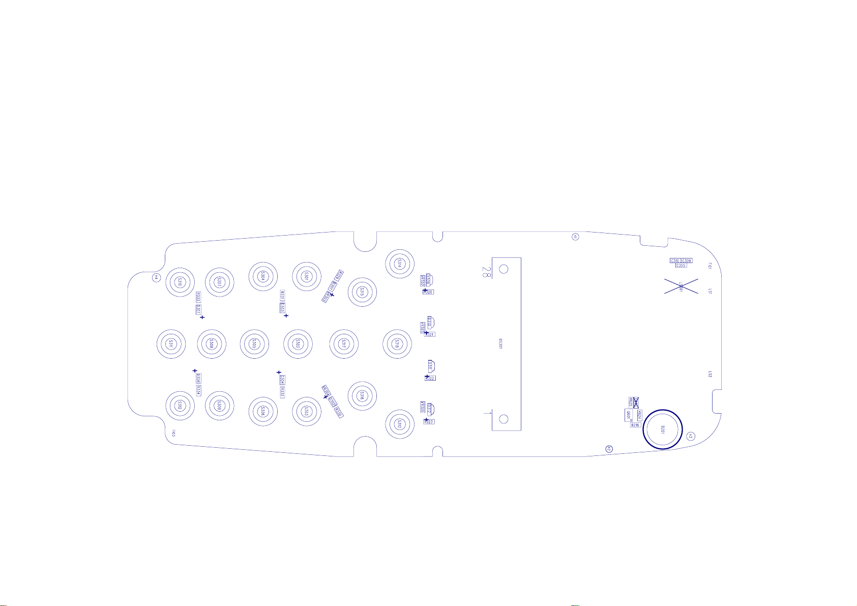
Chapter 5. Test Point Data
5-1 Component Side (1-1)
14
123
4138
9561071211
-37-
Page 38

-38-
Page 39

Loca-
tion
Component Side (1-1)
Battery connector : For damage or cold soldering cause power on failure1 J103
Nausica_CS : analog baseband chipset (ABB)2 U202
Hercrom20 : digital baseband chipset (DBB)3 U201
16Mbit flash ROM : For damage or cold soldering cause power on failure4 U304
5 Q101
6 Q301
7 Q302
9 J104
R104
13
14 D313
R105
R109
P-channel MOSFET with schottky diode : For damage or cold soldering
Cause charger function failure
Isolated dual transistors : For damage or cold soldering Q301A cause
vibration motor Failure, Q301B cause keypad back-light failure
Isolated dual transistors : For damage or cold soldering Q302A cause
pre-charger indication failure, Q302B cause the LCD back-light failure
Vibration motor : For damage or bad connection cause vibrator failure.8 J301
System connector : For damage or cold soldering cause headset failure,
trace/debug /SW download failure
SIM connector : For damage or bad connection cause SIM card failure.10 J102
Audio amplifier : For damage cause speaker function failure.11 U302
32.768kHz crystal : For damage cause RTC function failure.12 Y201
8P4R resistor network : For damage or cold soldering cause
trace/debug /SW download failure
Switching diode array : For damage or cold soldering cause the surge
noise by Vibrator
- 39 -
Page 40

- 40 -
Page 41

5-2 Component Side (1-2)
26
3222212425293130332327
28
-41-
Page 42

-42-
Page 43

Loca-
tion
Component Side (1-2)
21 C223
22 C224
23 C225
24 C226
25 C227
26
27 C206
28 R208
29
C207
C208
R301
C304
C305
VR2B regulator (2.85V) : For damage or cold soldering cause power
supply for DBB & ABB peripheral failure.
VR1B regulator (2V) : For damage or cold soldering cause power
supply for ABB internal logic failure
VR3 regulator (2.85V) : For damage or cold soldering cause power
supply for ABB analog circuits failure
VR2 regulator (2.9V) : For damage or cold soldering cause power
supply for Memory device failure.
VR1 regulator (1.8V) : For damage or cold soldering cause power
supply for DBB Core & RTC failure
SIM regulator (3V/5V) : For damage or cold soldering cause power
supply for SIM Interface failure
VREF output (1.2V) : For damage or cold soldering cause power
supply for power on failure
IBIAS output : For damage or cold soldering cause power supply for
Power on failure
Microphone Input : For damage or cold soldering cause microphone
failure
30
31
32
33 R204
R110
C107
C106
R107
R207
C205
Ext. audio Input : For damage or cold soldering cause external audio
input failure
Ext. audio output : For damage or cold soldering cause external audio
output failure
ABB local Osc. generator : For damage or cold soldering cause ABB
local Osc. failure
SIM card power control : For damage or cold soldering cause
SIM card power control failure.
- 43 -
Page 44

- 44 -
Page 45
5-3 Keypad Side (2-1)
1
235
4
-45-
Page 46

-46-
Page 47

Loca-
tion
Keypad Side (2-1)
1 DS301
D301~
2
D312
S301~
3
S317
5 Q601
LCM Connector : For damage or cold soldering cause LCD Display
failure
Back-Light LED : For damage or cold soldering cause back-light LED
failure
Keypad Switches : For damage or shirt circuit cause keypad function
failure
Backup Batter: For damage or cold soldering cause RTC function failure4 B201
T/R Switch transistor : For damage or cold soldering cause T/R Switch
function failure
- 47 -
Page 48

Chapter 6. Assembly Instructions
1. Remove Battery Cover
2. Remove Battery
- 48 -
Page 49

3. Remove Screws
4. Turn Handset Up
There are 4 screws in total
5. Take off Front Panel
- 49 -
Page 50

6. Take off Keypad & Metal-Dome
7. Take off Mainboard
- 50 -
Page 51

8. Take off Battery Connecter & MIC & Vibrator
Battery Connecter Vibrator
9. Turn Mainboard Down
MIC
- 51 -
Page 52

10. Take off Antenna
11. Take off Shielding Cover
- 52 -
Page 53

Chapter 7. Block Diagram
1. RF Section
- 53 -
Page 54

2. Baseband Section
Flash SRAM
Keypad
LCD
RF Interface
ARM 7
HERCROM 20
C54X
Codec
Nausica_CS
Vibrator
Backlight
System
Connector
Microphone
Battery
PM
Speaker
SIM Charger
- 54 -
Page 55

Baseband Top Schematic
Top Schematic
Baseband
Top Schematic
RF
Baseband
Peripheral
Baseband
Chip-set
Chapter 8. Circuit Diagram
-55-
/RESET_RF
TXVCO_ON
RADIO_TEMP
/PA_ON900
/PA_ON1800
PA_LEVEL
TCXOEN
TCXOBUFEN
CLK
DATA
TX_ON
13MHZ
AFC
VR2B
VBAT
Clara RF
IP
IN
QP
QN
EN
IP
IN
QP
QN
CLK
DATA
EN
/RESET_RF
TX_ON
TXVCO_ON
RADIO_TEMP
/PA_ON900
/PA_ON1800
PA_LEVEL
13MHZ
AFC
TCXOEN
TCXOBUFEN
VR2B
VBAT
100 Baseband Top Schematic
600 Clara RF
Page 56

CLK
-56-
I/O
J104
DSR_DAICLK
RXD_DAIRX
TXD_DAITX
RTS_DAIFS
CTS
ACCDET
RXD2
TXD2
SPKN
SPKP
MICP
MICN
GND
GND
RPWRON
VCHARGE
VCHARGE
VBATT
GT051-18P-LSS-SB-NB
R102 20k
IP
IN
QP
C103
1u/16V
VBAT
VBAT
C105
22p
VR113 VPORT0402 220K
C112
47p
QN
CLK
DATA
EN
/RESET_RF
TX_ON
TXVCO_ON
RADIO_TEMP
/PA_ON900
/PA_ON1800
PA_LEVEL
13MHZ
AFC
TCXOEN
TCXOBUFEN
VR2B
VBAT
C102
22n
HSP105
4
3 5
8 2
R101
0.22R
C101
10u
HSP106
HSP107
Q101
Si4833DY
HSP122
6
17
J103
4
3
2
1
C07-101
123
RST
VCC
HSP101
TP102
TP101
VR111 VPORT0402 220K
HSP102
HSP140
HSP138
HSP139
GND
VPP
P30-101-0209
J102
567
1
2
3
4
5
6
7
8
9
10
11
12
13
14
15
16
17
18
12
12
HSP141
HSP142
HSP143
HSP144
HSP145
D101 P0402FC08C
D104 P0402FC08C
VR112 VPORT0402 220K
HSP103
HSP137
HSP104
HSP136
VR109 VPORT0402 220K
VR110 VPORT0402 220K
VR108 VPORT0402 220K
C104
100n16V
HSP134
HSP135
VR106 VPORT0402 220K
VR107 VPORT0402 220K
HSP133
HSP132
HSP131
VR103 VPORT0402 220K
VR104 VPORT0402 220K
VR105 VPORT0402 220K
VR102 VPORT0402 220K
R104A MNR04-47R
1 2
R104B MNR04-47R
3 4
R104C MNR04-47R
5 6
R104D MNR04-47R
7 8
R105A MNR04-47R
1 2
R105B MNR04-47R
3 4
R105C MNR04-47R
5 6
R105D MNR04-47R
7 8
R107 4R7
R108 4R7
R110 47R
R114 4R7
R106 0
VR101 VPORT0402 220K
VBAT
R109A MNR04-10k
1 2
R109B MNR04-10k
3 4
R109C MNR04-10k
5 6
R109D MNR04-10k
7 8
R115 10k
R111 100k
C111
47p
C107 100n
C106 10u
C113 10u
C114
47p
200 Baseband Chip-set
VR2B
C110
47p
DSR_DAICLK
RXD_DAIRX
TXD_DAITX
RTS_DAIFS
CTS
ACCDET
RXD2
TXD2
RPWRON
HOOKDETECT
AUXI
AUXI_O
SIM_I/O
SIM_CLK
SIM_RST
SIM_VDD
Baseband Chip-set
EARN
MICIN
AUXOP
SHUTDOWN
VIBRATOR
/WR
/RD
FDP
AUXOP
SHUTDOWN
AUXON
AUXON
BACKLIGHT
VIBRATOR
BACKLIGHT
FWP
/RD
/WR
FDP
FWP
EARP
EARP
EARN
MICBIAS
MICBIAS
MICIN
MICIP
MICIP
ACCDET
ACCDET
VR2B
VBAT
IN
IP
EN
QN
QP
CLK
DATA
TX_ON
/RESET_RF
/BLE
/BLE
D[0..15]
/BHE
/CS2
/CS1
/CS0
A[0..21]
/RESET_OUT
D[0..15]
A[0..21]
/BHE
/CS1
/CS0
/CS2
D[0..15]
A[0..21]
/RESET_OUT
TXVCO_ON
RADIO_TEMP
KBC[0..3]
PA_LEVEL
/PA_ON900
/PA_ON1800
KBC[0..3]
KBR[0..4]
KBR[0..4]
KBR[0..4]
KBC[0..3]
AFC
13MHZ
TCXOEN
TCXOBUFEN
END_ON/OFF
END_ON/OFF
VBAT_2
BATT_ID
BATT_TEMP
VR2B
VBAT
VCHG2
VCHG2
VR2B
VBAT
ICTL
R103A MNR02-1k
1 2
R103B MNR02-1k
3 4
HSP121
VR2
VR2B
VBAT
VR2
VR2B
VBAT
VR2
VCHG
VR2
Baseband Peripheral
1
300 Baseband Peripheral
Page 57

BACKLIGHT
-57-
/RESET_OUT
VIBRATOR
SHUTDOWN
ACCDET
RXD_DAIRX
DSR_DAICLK
RTS_DAIFS
TXD_DAITX
TCXOEN
TCXOBUFEN
/RESET_RF
/PA_ON1800
/PA_ON900
TXVCO_ON
TX_ON
D[0..15]
A[0..21]
KBC[0..3]
KBR[0..4]
FWP
CTS
RXD2
TXD2
CLK
DATA
/WR
/RD
/CS2
/CS1
/CS0
/BLE
/BHE
FDP
EN
D[0..15]
A[0..21]
R221 n.m
R222 n.m
R223 n.m
R224 0402-R-Short
R225 n.m
R226 0402-R-Short
R227 0402-R-Short
R228 0402-R-Short
R229 0402-R-Short
U201
ULYSSE_179uBGA_HERCROM20
E14
TSPCLKX
D14
TSPDO
C13
TSPACT00
B13
TSPACT01
B12
TSPACT02
D11
TSPACT03
B10
TP227
TP206
TP207
BaseBand supply overview :
------------------------------------------------------VR1 (1.8V) Digital core & RTC Permanent
VR1B 2.0V Nova internal logic ON/OFF
VR2 2.0/2.9V Memory devices Permanent
VR2B 2.9V Nova & Samson peripherals Permanent
VR3 2.9V Nova analog supply ON/OFF
D0
D1
D2
D3
D4
D5
D6
D7
D8
D9
D10
D11
D12
D13
D14
D15
A0
A1
A2
A3
A4
A5
A6
A7
A8
A9
A10
A11
A12
A13
A14
A15
A16
A17
A18
A19
A20
A21
TSPACT04
E9
TSPACT05
E8
TSPACT06 nCS6
E7
TSPACT07 CLKX_SPI
C6
TSPACT08 nMREQ
E6
TSPACT09 MAS1
H10
TSPACT10 nWAIT
K13
TSPACT11 MCLK
D13
TSPEN0
D12
TSPEN1
B14
TSPEN2
C12
nSCS2 TSPEN3
P9
DATA00
K9
DATA01
P10
DATA02
N10
DATA03
K10
DATA04
P11
DATA05
M11
DATA06
L11
DATA07
N12
DATA08
P13
DATA09
N13
DATA10
M13
DATA11
M12
DATA12
N14
DATA13
M14
DATA14
L13
DATA15
J4
ADD00
K1
ADD01
K2
ADD02
K4
ADD03
L1
ADD04
L2
ADD05
L3
ADD06
M1
ADD07
N1
ADD08
M3
ADD09
M2
ADD10
N2
ADD11
P2
ADD12
N3
ADD13
L4
ADD14
N4
ADD15
P4
ADD16
K5
ADD17
L5
ADD18
N5
ADD19
P5
ADD20
K6
ADD21 CLK16X_IRDA
/CS2
/CS1
/CS0
/BLE
/BHE
FDP
KBC[0..3]
KBR[0..4]
RnW
nFOE X_A(3)
nCS2
nCS3
CS4 ADD22
nCS0
nCS1
TIME
SERIAL
PORT
MEMORY
INTERFACE
nBLE I/O15
nBHE I/O14
K8K7P6L7P7M7M8N8L8
nFWE X_A(0)
FDP nIACK
L9
M9
C1E3F4
C4
SDO INT0n
MICROWIRE
INTERFACE
KBC3 XDI_O1
KBC2 XDI_00
KBC4 XDI_O2
E5
D5
KBC2
KBC1
KBC3
SDI SDA
nSCS0 SCL
SCLK INT1n
G5
nSCS1 X_A(2)
IRDA PORT
DAICLK
DAIFS
DAIRX
DAITX
CTS
RXD
DSR
RTS
TXD
F2F1D1D2E4
E1
F3
TX_IRDA
RX_IRDA
X_A(4 ) TXIR_IRDA
X_A(1) RXIR_IRDA
CLKOUT_DSP SD_IRDA
F5
TX-MODEM
DSR-MODEM LPG
RTS-MODEM TOUT
SERIAL
INTERFACE
A9D9D8
D3
E2
RX_MODEM
CTS_MODEM XF
MCSI
INTERFACE
R201 0402-R-Short
R202 0402-R-Short
R203 0402-R-Short
B9
TXD_MCSI I/O9
CLK_MCSI I/O11
RXD_MCSI I/O10
FSYNCH_MCSI I/O12
ULYSSE
HERCROM20
VDDS1
VDDS1
VDDS1
VDDS2
VDDS1
VDDS2
VDDS2
XDI_O6 KBR3
XDI_O7 KBR4
KBR3
KBR4
G12
VDDA1
A14
D10
K12
VDDS2
P14
C3
VR205 VPORT0402 220K
VDDS1
J10
VR204 VPORT0402 220K
KBC0 NFIQ
kBC1 NIRQ
A6A5B5
A4B4D4B3A2
KBC0
XDI_O3 KBR0
XDI_O4 KBR1
XDI_O5 KBR2
KBR0
KBR2
KBR1
A10
H5
E11
TCXOEN
RFEN nOPC
EN_LMM_PWR X_IOSRB
POWER
MANAGEMENT
VDD
VDDLMM
VDD
VDD
VDD
F10A3B8M5A13
J5P8K3L6N9
VR203 VPORT0402 220K
J1J3M4
I/O00 TPU_WAIT
GENERIC I/O
POWER SUPPLYKEYBOARD INTERFACE
VDDLMM
VDDLMM
M6
G10
C14
I/O02 IRQ4
TSPDI I/O4
I/O6 BCLKX
I/O3 SIM_RnW
I/O01 TPU_IDLE
VDDARM
P12
C218
C219
100n
100n
H14
GNDA1
F11
K11
ARMCLK BCLKR
I/O7 NRESET_OUT
MISCELLANEOUS
GND
GND
GND
GND
L12
M10
N6
P1
C220
100n
C2
B1
C9
IDDQ
PWL LT
PWT BU
OMEGA
INTERRUPTS
JTAG & DEBUG
BASE BAND
INTERFACE
VOICE BAND
INTERFACE
ARM SERIAL
PORT (SPI)
SIM
INTERFACE
GND
GND
GND
GND
GND
J2C5C10P3A12B2N7
E12
L10
C222
C221
100n
100n
1 2
B11
E10
A11
GNDA2
OSC32K_IN
CLKTCXO
START_BIT CLK13M_OUT
ON_OFF
nRESPWON
INT4n IT_WAKEUP
EXT_FIQ
EXT_IRQ
nEMU0
nEMU1
nBSCAN
VFSRX
VCLKRX
MCUDI
MCUDO
MCUEN0
MCUEN1 I/O8
MCUEN2 I/O13
SIM_IO
SIM_CLK
SIM_RST
SIM_CD MAS0
SIM_PWCTL I/O5
GNDLMM
GNDLMM
GND
GNDLMM
GNDARM
N11
C201
n.m
C203
18p
3
Y201
MS1V-TK
32.768kHz
C11
CLK32K_OUT
OSC32K_OUT
TDI
TDO
TCK
TMS
BFSR
BDR
BFSX
BDX
VDX
VDR
TP213
TP215
TP217
TP216
TP214
TP212
VR1VR1
C202
n.m
C204
18p
TP205
UPR
R209
10k
G14
L14
U202
PTWL3012GGM
D201
RB751S-40
D10
ONnOFF
F6
RESPWRONZ
D7
RTC_ALARM
F7
INT1
H4
INT2
F2
TESTRESETZ
C8
TEST1/BULON
B8
TEST2/BULENA
A9
TEST3/BDLON
B9
TEST4/BDLENA
C7
TDO
A7
TDI
B7
TCK
A8
TMS
J5
BFSX
K5
BDX
G5
BFSR
H5
BDR
K7
VDR
G6
VDX
G7
VFS
H6
VCK
J6
UDX
K6
UDR
F5
UEN
B2
SDIO3
C4
SCLK3
B3
SRST3
VBAT_2
K3
VCC1
D2
VCC2
G9
VCC3
K2
SWITCH
J1
FDBK
H3
COMP
E2
VR2IN
D3
VR2SEL
H1
VR1OUT
E1
VR2OUT
H10
VR3OUT
C1
VR1BOUT
D1
VR2BOUT
R217 10k
C216
C215
100n
100n
D6
G3
B6
D7
E13
G2
G4
H4
TP218
H2
H3
G1
H1
F12
F13
F14
G13
H12
H13
H11
G11
A8
C8
C7
B7
A7
J13
J14
K14
J11
J12
R204 20k
VR3
VR2B
VR1B VR2VR1
C224
C223
10U
C225
2u2
10U
R211 10k
VR2B
R205
0402-R-Short
UPR
2 1
C226
C229
n.m
C227
10U
10U
UPR
C217
100n
TDO_ARM
R207
22k
C205
18p
A10
B10
F1
PWON
OSCAS
ON/OFF &
INTERRUPT
CONTROL
DEBUG &
TEST
BASE BAND CODEC
Nausica
VOICE BAND CODEC
MCU
SERIAL PORT
SIM
LEVEL SHIFTER
VOLTAGE
REGULATORS
GNDR1
GNDR2
GNDR3
K1
C2
G10
TDI
RPWON
TMS
J4
K4
TDR
TIME
SERIAL
PORT
MISC.
ANALOG
I/O
BATTERY
MANAGEMENT
CURRENT/
VOLTAGE
REFERENCES
REFGND
F3
TCK
TEN
TDO
A4
LCDSYNC
CK13M
TSCXP/ADIN4
TSCYP/ADIN5
VBACKUP
TP209
TP210
VR2B
TESTRESET
VR201 VPORT0402 220K
UPR
R206
100k
C212 1n
VR202
VPORT0402 220K
C5
A6
TSCYM
B6
TSCXM
B5
ADIN1
A5
ADIN2
E6
ADIN3
D6
C6
F10
DAC
F8
AFC
F9
APC
G8
AUXGND
E10
BDLQM
E9
BDLQP
E8
BDLIM
E7
BDLIP
R210A
D9
BULQM
R210B
D8
BULQP
R210C
C10
BULIM
R210D
C9
BULIP
MNR04-1k
MNR04-1k
MNR04-1k
MNR04-1k
K9
MICBIAS
H7
AUXI
J7
AGNDA1
K8
MICIP
J8
MICIN
H9
EARP
H8
EARN
J9
AUXOP
J10
AUXON
K10
BUZZOP
A3
VAUX
A1
VS2
B1
VS1
C207 220n
A2
SVDD
D4
SDIO5
B4
SCLK5
D5
SRST5
C3
UPR
J3
E5
VBAT
E4
VCHG
E3
ICTL
C214 100n
G4
BGTR1
G3
BGTR2
G2
BGTR3
H2
BGTR4
J2
BGTR5
G1
IBIAS
F4
VREF
C206
100n
Title
Size Document Number Rev
A2
Date: Sheet
I J
C211 33n
1 2
3 4
5 6
7 8
UPR
VBAT
C209 470p
C208 1u
R216 270R
C213 100n
C228
47p
C210 470p
C231 47p
TP228
R208
120k
1 2
1 2
3 4
5 6
7 8
B201 PHR0621S-VE5
VBAT_2
B1300 Baseband Chipset
<Doc> 2.2
13MHZ
END_ON/OFF
RPWRON
BATT_ID
BATT_TEMP
RADIO_TEMP
HOOKDETECT
AFC
PA_LEVEL
R215A
R215B
R215C
R215D
MNR04-1k
MNR04-1k
MNR04-1k
MNR04-1k
C232 47p
Place C231 and C232 as
close to Nausica as
possible
VBAT
VR2B
VR2
Lite-On Technology Corp.
of
11Wednesday, January 22, 2003
QN
QP
IN
IP
MICBIAS
AUXI
MICIP
MICIN
EARP
EARN
AUXOP
AUXON
SIM_VDD
SIM_I/O
SIM_CLK
SIM_RST
VCHG2
ICTL
VBAT_2
VBAT
VR2B
VR2
1
Page 58

ACCDET
-58-
EAR_PHONE
AUXI_O
MICBIAS
MICIP
MICIN
Microphone
Receiver/Speaker
EARP
AUXOP
EARN
AUXON
SHUTDOWN
R302
0402-R-Short
C353
10u
C356
47p
C337
47p
C357
47p
C341
47p
R303
n.m
EAR_PHONE
C304 100n
C305 100n
R356 120k
R304 4k7
R357 120k
R325 4k7
R355
2k2
R301
3k3
HSP301
C306 1u
C339 1u
VR301
VPORT0402 220K
C334
47p
R352 4R7
R354 4R7
R353 47R
C352
n.m.
C301
47p
2
1
R326
9k1
C332
47p
C351
n.m.
HSP362
M301
OB-22S42-C1033
C330
47p
C331
47p
C340
n.m.
C307
1u
VR2B
R351
120k
HSP361
VR307 VPORT0402 220K
4
3
2
1
CN301
HEADJACK
2
3
4
1
VR2
VR2B
VBAT
U302
TPA751DGN
IN-
IN+
BYPASS
nSD
C333 47p
C308 3n9
R306 9k1
9
GND
VR2
VR2B
VBAT
Place C331 and C338 as
close to TPA751DGN as
possible
6
VDD
5
Vo+
8
Vo-
7
GND
VBAT VBAT VBAT
BL-HB334E-TRB Blue
D303
D301
12
R329
6R8
BACKLIGHT
D302
12
R330
6R8
D307
D308
D304
12
12
12
12
R331
R332
R333
6R8
6R8
6R8
R338
1k
2
3 4
R308
680
Backlight
This portion place to top side
VBAT
C329 1u/16V
C313 47p
C338
47p
C312
47p
C311
47p
of PCB near to speaker/receiver
R334
6R8
Q301B
IMX9
R310
6R8
R0603
END_ON/OFF
VCHG2VCHG
R319
R327
10R
34
R318
56R
0805
R320
15R
12
D309
C355
47p
C310
47p
47R
6
5
Q302A
1
IMT17
BL-HB536A-TRB Blue
R321
R322
15R
15R
12
12
D311
D310
The magnetic part of
BRS-241302P should
be connected to GND
LS301
BRS-241302P
C309
HSP303
47p
12
R323
15R
D312
1
2
HSP302
R316
4K7
2
Q302B
IMT17
R317
3K3
KBC[0..3]
KBR[0..4]
Keypad
Vibrator
KBR0
KBR1
KBR2
KBR3
KBR4
VIBRATOR
VPORT0402 220K
HSP326
HSP327
HSP331
HSP330
HSP333
HSP334
HSP337
HSP340
HSP339
HSP323
HSP322
HSP321
HSP320
HSP319
VR302
HSP325
HSP329
HSP332
HSP335
HSP338
HSP324
HSP328
R339
1k
KBC0
VPORT0402 220K
HSP318 HSP313
HSP317
HSP316
HSP315
HSP314
VR303
S314
KSW
[OFF-HOOK]
S301
KSW
[1]
S304
KSW
[4]
S307
KSW
[7]
S310
KSW
[*]
VBAT
C335
n.m
5
R335
100k
KBC1
HSP312
HSP311
HSP310
HSP309
VR304
VPORT0402 220K
S315
KSW
[BOOK]
S302
KSW
[2]
S305
KSW
[5]
S308
KSW
[8]
S311
KSW
[0]
231
D313
DA221
1
Q301A
IMX9
6
KBC2
VPORT0402 220K
VPORT0402 220K
VBAT
C314
680p
HSP304
[C]
HSP305
HSP308
HSP307
[3]
[6]
[9]
[#]
1
2
VR306
VR305
S316
KSW
S303
KSW
S306
KSW
S309
KSW
S312
KSW
J301
LA4-436BB1
KBC3
[DOWN]
[UP]
HSP306
S317
KSW
S318
KSW
S313
KSW
[ON-HOOK/PWR]
D[0..15]
A[0..21]
/RESET_OUT
LCD Display
VR2B
7 8
5 6
3 4
1 2
7 8
5 6
3 4
1 2
1 2
3 4
5 6
7 8
C318
n.m
C328
n.m
VR310 VPORT0402 220K
HSP353
HSP354
HSP352 HSP336
HSP351
HSP349
HSP350
HSP348
HSP346
HSP347
DS301
1
VDD
2
C86
23
D0
22
D1
21
D2
20
D3
19
D4
18
D5
17
D6
16
D7
24
RD - E
25
WR - R/W
26
A0
28
CS
27
RES
G112064-23
HSP345
HSP344
HSP341
HSP343
HSP342
Title
B1300 Baseband Peripheral
Size Document Number Rev
<Doc> 2.2
A2
Date: Sheet
I J
C322
13
C3N
1u/16V
12
C1P
C321
11
C1N
1u/16V
10
C2N
C320
9
C2P
1u/16V
8
V2
7
V3
6
V4
5
V5
4
V6
14
VEE
C319
1u/16V
3
VSS
15
VSS
HSP359
Lite-On Technology Corp.
HSP357
HSP358
HSP356
HSP355
C327
1u/16V
C326
1u/16V
C325
1u/16V
C324
1u/16V
C323
1u/16V
VR2B
of
11Wednesday, January 22, 2003
D[0..15]
A[0..21]
U303
K6F4016U4D
D0
B6 A3
I/O0 A0
D1
C5
I/O1
D2
C6
I/O2
D3
D5
I/O3
D4
E5
I/O4
D5
F5
I/O5
D6
F6
I/O6
D7
G6
I/O7
D8
B1
I/O8
D9
C1
I/O9
D10
C2
I/O10
D11
D2
I/O11
D12
E2
I/O12
D13
F2
I/O13
D14
F1
I/O14
D15
G1
I/O15
E1
VR2
/BHE
/BLE
/WR
/RD
/CS2
/CS1
/CS0
FDP
FWP
/BHE
/BLE
/WR
/RD
/CS2
/CS1
/CS0
FDP
FWP
/RESET_OUT
Vcc
D6
Vcc
D1
GND
E3
NB
E6
GND
H6
NC
G2
NC
A1
A2
A4
A1
A3
A5
A2
A4
B3
A3
A5
B4
A4
A6
C3
A5
A7
C4
A6
A8
D4
A7
A9
H2
A8
A10
H3
A9
A11
H4
A10
A12
H5
A11
A13
G3
A12
G4
A13
A15
F3
A14
A16
F4
A15
A17
E4
A16
A18
D3
A17
A19
H1
DNU
B5
CS
A6
VR2
DNU
A1
LB
B2
UB
A2
OE
G5
WE
VR2
U304
D0
E2
D1
D2
D3
D4
D5
D6
D7
D8
D9
D10
D11
D12
D13
D14
D15
DQ0
H2
DQ1
E3
DQ2
H3
DQ3
H4
DQ4
E4
DQ5
H5
DQ6
E5
DQ7
F2
DQ8
G2
DQ9
F3
DQ10
G3
DQ11
F4
DQ12
G5
DQ13
F5
DQ14
G6
DQ15
G4
Vcc
F6
BYTE
C316
100n
H1
H6
A3
Vss
Vss
RY/BY
Am29LV160B
RESET
WP/ACC
A1
E1
A0
A2
D1
A1
A3
C1
A2
A4
A1
A3
A5
B1
A4
A6
D2
A5
A7
C2
A6
A8
A2
A7
A9
B5
A8
A10
A5
A9
A11
C5
A10
A12
D5
A11
A13
B6
A12
A14A14
A6
A13
A15
C6
A14
A16
D6
A15
A17
E6
A16
A18
B2
A17
A19
C3
A18
A20
D4
A19
A21
D3
A20
A4
WE
G1
OE
B4
B3
F1
CE
R315 10k
VR2
/RD
/WR
/CS2
/RESET_OUT
R311D MNR04-100R
D0
R311C MNR04-100R
D1
R311B MNR04-100R
D2
R311A MNR04-100R
D3
R312D MNR04-100R
D4
R312C MNR04-100R
D5
R312B MNR04-100R
D6
R312A MNR04-100R
D7
R313A MNR04-100R
R313B MNR04-100R
A0
R313C MNR04-100R
R313D MNR04-100R
R314 100R
C317
n.m
Page 59

VRF2
-59-
TXVCO_ON
R601
220R
C604
4n7-5%
ECHU
TCXOBUFEN
TCXOEN
AFC
13MHZ
TX_ON
PA_LEVEL
VBAT
/PA_ON1800
/PA_ON900
VR2B
CLK
DATA
EN
/RESET_RF
QN
QP
IN
IP
RADIO_TEMP
TO/FROM BASEBAND
123
47k
L614
6n8
C602
1n
10k
12
D601
HVC369B
Q603
DTA114YE
C601
5p6
C645
1n
C649
4U7-X5R
ACTIVE CIRCUITRY:
TX Main PLL + Main VCO
Aux PLL + Aux VCO
Offset PLL + TX/RX VCO
RX Main PLL + TX/RX VCO
C665
120p
R609 33R
C613
1n, COG
C648
C647
10n
n.m
C650
4U7-X5R
C666
n.m
C614
100p
C646
27p
C667
n.m
R610 33R
C664
100n
13
C651
4U7-X5R
8
9
LB_ON
HB_ON
TX_ON
CTRL
GND
5
712
Y601
VON1885C28DKB
TX/RX VCO
VRF3
VRF2
VRF3
12
R612
0402-R-Short
11610
RX
HB
Vcc
TX
RX
LB
TX
14
U601B
PTRF6150
47
46
45
DETD
DETR
FILT
VAPC
48
vhome
I
LPF
Vcc3
APC
APCEN
8
C617
27p
C671
1p
4
3
R614
R613
1k5
1k2
TX_1800
TX_900
TP606
R640
1k
C636
22p
VRF3
R616
6R8
34
12
R615B
R615A
680R
680R
R618
6R8
12
34
R617A
R617B
680R
680R
C663
680p
C631
4U7-X5R
C630
n.m
U603
RF3110
1
DCS_PCS_IN
7
GSM_IN
Low = GSM
High = PCN
C633
47p
Transmitter
131415161718192021222324252627282930313233343536373839
GND
GND
GND
GND
GND
GND
GND
GND
GND
GND
GND
GND
GND
GND
GND
GND
GND
GND
GND
GND
GND
B_SW
PA_EN
VRAMP
2
3
6
C634
12p
VBATT
4
VREG
VCC2_GSM
5
89101112
GND
GND
VCC_OUT
40
GND
GND
GND
GND
VCC2_DCS_PCS
HSL1
STRIPLINE-inn
GND
DCS_PCS_OUT
GSM_OUT
Frontend
U601C
PTRF6150
I/Q
Receiver
RXmixQp
RXmixQn
25
26
C620
1n
Main PLL
RXmixIp
27
C619
1n
L604
DCS1nan
DCS1nap
PCS1nan
x2
PCS1nap
90
GSM1nan
:2
GSM1nap
GNDlna
DECRXmix
RXmixIn
28
30
C618
n.m
1n8
44
43
L605
1n8
41
40
L606
10n-5%
37
36
L607
39
10n-5%
C635
n.m
12p
C626
C624
C627
n.m
12p
C625
n.m
C670
n.m
R624
47k
U602
FEM8450T
5
2
15
ANT
TX-900
TX-1800
9
RX-1800A
10
RX-1800B
13
RX-900B
12
RX-900A
C628
47p
VRF3
Title
Size Document Number Rev
A2
Date: Sheet
I
3
GND
6
GND
7
GND
8
GND
11
GND
14
GND
16
GND
VC2
VC1
Switch TX900 TX1800 RX900/RX1800
VCC1 2.8 V 0 V 0 V
1
4
VCC2 0 V 2.8 V 0 V
C629
12p
Q601
Si1905DL
1
6
2
5
3 4
VRF3
B1300 Clara RF
<Doc> 2.2
9
J600
MS-147
12
3
4
C615
n.m
R625
47k
Lite-On Technology Corp.
ANT-PAD-2_0-LGH
L608
3.3nH
11Monday, January 27, 2003
TP605E601
1
C616
n.m
1
of
L613
Main VCO
100n
R634
2k7
C660
6p8
L601
2n7
C603
33n-5%
ECHU
R602
1k2
VRF2
C622
2p7
C623
2p7
R603
680R
U601D
PTRF6150
C637
n.m
C608
100n
2
Q602
2SC5010
R619
1 3
6k8
C632
R637
5p
100R
CRF
Test
29
C609
68p
R605
2k2
4
MainSPUP1
Main
PLL
Aux
PLL
VCO
L603
120n
R638
68R
C605
27p
53454
MAINcp
AUXcp
142324
Main
AUXvcop
C653
1n
C621
27p
53
VCO
RX1op
RX1on
S
Q-Mod
I/Q
S
AUXvcon
C668
27p
AUX VCO
C662
100n
51
OMIXrf
PFD/CP
L609
15n-LQP-type
VRF2
6412
LBswitch
HBswitch
56
C657
33p
C658
33p
TXRXswitch
RX
TX
MainSPUP2
T
GNDtxcp
C606
3p9
C607
3p3
Synthesizer
Z601
LDB25D500A0013A
5
7 8
NCLNC
GND
1
R3
60
TXRXcp
59
R607
82R
R2
58
5716
RX
R606
1k8
D602
L612
HVC369B
22n
1 2
L602
120n
R604
2k2
C611
15n-5%
ECHU
H
GND
346
C610
2n2-5%
2
C669
n.m
C612
12n
ECHU
R608
3k3
13 MHz
R633
4
VCC
GND
GND
8
TP603
R632
0402-R-Short
OUT
Y602
TOA1300VPM4DKG-SM2
GND
U601A
PTRF6150
PG3.0
Vbat3
61
Vbat2
6
Vbat1
50
VR4in
10
CLK
11
DATA
12
EN
13
17
ResetZ
QN
18
QP
19
IN
20
IP
21
TP604
15R
I/Q
RX &
TX
Reg 3
Reg 2
Reg 1
Seriel
R631
15R
C655
n.m
C638
n.m
1 2
3 4
5 6
7 8
MNR04-1k
C654
2u2
1
R628A
R628B
R628C
R628D
CTL
TP601
GND
23567
TP602
GND
C656
1u
C652
1n
R630
560R
LNA/TX offset mixer - Vcc2
Demod / PA Ctrl - Vcc3
RX Buf / TX PFD - Vcc4
Interface
RX BB / VCO Buf - Vcc1
AUX PLL / 13Mhz - Vcc9
53
2 4
R629
1M
TX CP - Vcc6
Main VCO core - Vcc8
Main CP - Vcc5
AUX VCO - Vcc7
Main Counters - Vcc10
Bandgap
BIASref
GND
65
35
C639
R627
n.m
9k76 1%
U604
SN74AHC1GU04DCKR
Peripherals
Vreg3
62
Vreg2
7
Vreg1
49
38
42
52
55
33
63
22
15
3
32
31
C640
100n
VRF1
C642
C643
n.m
1p
C641
C644
n.m
5p6
Page 60

-60-
Page 61

Chapter 9. Tooling List
Level 1
DUMMY BATTERY
TEST SIM CARD
ANTISTATIC GLOVE
ESD COMPONENT BOX ( SMALL )
ESD COMPONENT BOX ( BIG )
ESD WRIST STRIP
ESD TRAY
FUNCTION
Pick up small part
Screwing
Clean lens
Clean hand set
For testing
SPECITEM
Motic 20x~80MAGANIFY(20 TIME )
8*22 mmDOUBLE TAPY ( 3M)
ELMTAPE CUTER MACHINE
3CPINCES
HIOS CL3000SCREW DRIVE
3M Model 908ELIMINATOR AIR GUN
15*15 CMLONG FIBER CLOTH
ANTISTATIC TABLE CLOTH
SCREW FEEDER
HAND SCREW DRIVE
- 61 -
Page 62

Level 2
Buzzer/Mic Replace
LED Replace
Murcury Battery Replace
DUMMY BATTERY
FUNCTION
Screwing
Clean lens
Clean hand set
For testing
SPECITEM
Weller WES50SOLDER STATION
Kester 0.6mmSOLDER WIRE
Fmkanc32-200FLUX PASTE
Motic 20x~80xMAGANIFY(20 TIME)
8*22 mmDOUBLE TAPY (3M)
ELMTAPE CUTER MACHINE
3CPINCES Pick up small part
HIOS CL3000SCREW DRIVE
3M Model 908ELIMINATOR AIR GUN
15*15 CMLONG FIBER CLOTH
PRINTER
SCANNER
PC
TEST SIM CARD
ANTISTATIC CLOTH
ANTISTATIC GLOVE
ANTISTATIC SHOES
ESD COMPONENT BOX ( SMALL )
ESD COMPONENT BOX ( BIG )
CLEANNER
CLEANNER BOTTLE
ESD WRIST STRIP
ESD TRAY
ANTISTATIC TABLE CLOTH
SCREW FEEDER
SOLDER IRON JIG
HAND SCREW DRIVE`
- 62 -
Page 63

Level 3
Buzzer/Mic Replace
LED Replace
Murcury Battery Replace
DUMMY BATTERY
FUNCTION
Screwing
Clean lens
Clean hand set
For testing
SPECITEM
Weller WES50SOLDER STATION
Kester 0.6mmSOLDER WIRE
Fmkanc32-200FLUX PASTE
Motic 20x~80xMAGANIFY(20 TIME)
8*22 mmDOUBLE TAPY (3M)
ELMTAPE CUTER MACHINE
3CPINCES Pick up small part
HIOS CL3000SCREW DRIVE
3M Model 908ELIMINATOR AIR GUN
15*15 CMLONG FIBER CLOTH
PRINTER
SCANNER
PC
TEST SIM CARD
ANTISTATIC CLOTH
ANTISTATIC GLOVE
ANTISTATIC SHOES
ESD COMPONENT BOX ( SMALL )
ESD COMPONENT BOX ( BIG )
CLEANNER
CLEANNER BOTTLE
ESD WRIST STRIP
ESD TRAY
ANTISTATIC TABLE CLOTH
SCREW FEEDER
SOLDER IRON JIG
HAND SCREW DRIVE`
- 63 -
Page 64

Chapter 10. Equipment List
Level 2
PC
Dummy Battery
Multimeter
OSC SCOPE
SPECTRUM
Level 3
HP 8960/HP 8922/R&S CMU200
HP 66311B (DC Power)
PC
GPIB Card (HP82350A)
FUNCTION
FUNCTION
SPECITEM
SPECITEM
Dummy Battery
Multimeter
OSC SCOPE
SPECTRUM
HP E6392B
- 64 -
Page 65

Chapter 11. Exploded View & Replacement Part List
-65-
11.1 Exploded View
M1M2M3M4M5M6M7M8M9
M10
M11
M12
M13
M18
M14
M15
M16
M17
Page 66

<Parts List of Exploded View>
No. Location No. LG Part No. GVC Part No. Description Service
M1 MDAL0002501 R2920002A0 B1300 bezel for LG Y
M2
M3
M4 LS301(BRS-241302P)
M5
M6
M7
M8 J103
M9
M10
M11
M12
M13
M14
M15 M301
M16 J301 (LA4-436BB1)
M17
M18
MWAZ0002901 R3870192R0 B1300 LENS FOR LG Y
MCJK0017802 R2710338R0 B1300 Front Case (SV) Y
SUSY0009201
MHGD0001701
SAFY0078401
SNGF0002201
ENZY0012801
ACGM0022802
MCCF0010801
SBPL0064501
MCJA0004502
MKAA0008401
ADCA0013701
SUMY0006601
SJMY0005701
GMZZ0009501
MCCC0010101
HJ001190M0 Speaker & Receiver BRS-241302P Y
R3850037Q0 LCM METAL SHEET1 0.2t Y
8404C699 Main Board + Keypad Y
R3930047M0 ANTENNA EMBEDED(IN BUILD ANTENNA) Y
R3010218M0 Battery connector C07-105-0029 Y
R2720244R0 B1300 Rear Case Assembly (SV) Y
R3814030J0 B1300 RUBBER CAP FOR ANTENNA Y
JB040094A0 BATTERY PACK,LI-ION Y
R2770040R0 B1300 Battery Cover (SV) Y
R392008110 B1300 P+R KEYPAD (Russia) Y
R401000810 B1300 METAL DOME Y
HJ11006590 MICRO PHONE OB-22S42-C1033 with Polymatech Y
R400001180 Vibrator 3V 11200rpm LA4-436BB1 Y
R3220072U0 MACHINE SCREW M1.6x3mm T6 Y
R3814033J0 B1300 RUBBER CAP FOR EAR-MIC Y
- 66 -
Page 67

11-2 Replacement Part List
Chip set
No. Location No. LG Part No. GVC Part No. Description Service
U201 CG010288B0 ASIC ULYSSE Hercrom200 DBBµBGA_179p N
U202 CG010438B0 ASIC Nausica_CS TWL3012GGM ABB µBGA_100p N
U601 CG01042DB0
IC ASIC Clara Transceiver TRF6150 S-PQFP-G64
Re3.1
N
Memory
Item Location No. LG Part No. GVC Part No. Description Service
U303 BB31911Y80 SRAM IC CHD416LVB-70 BGA 48P N
U304 BG16907YT0
Flash Memory IC 32Mbit dual-bank
AM29DL323GT90WMI
N
Electronic - Baseband Active
Item Location No. LG Part No. GVC Part No. Description Service
U302
Q101 DE04096YD0
Q301
Q302
D201
D313
#N/A
EQBN0013601
EQBP0007601
EDSY0011501
EDSY0011601
DA01043Y30 IC Audio Amplifier TPA751DGN S-PDSO-G8 N
IC MOSFET+Schottky Diode Si4833DY SO-8 Vishay
Siliconix
EAE1000340 TR NPN Pair IMX9 SMT6 Y
EBE1000240 TR PNP Pair IMT17 SMT6 Y
EJ12005840 Schottky Diode RB751S-40 SOD523 Y
EJE1001640 Diode Pair DA221 SOT416 Y
N
D301,D302,D303,D304
, D307,D308
D309,D310,D311,D312
Y201
D101,D104
EDLH0008901
EDLH0009001
EXXY0016101
#N/A
EL500290D0 LED 0816 BL-HB536E-TRB Blue Y
EL500289D0 LED 0622 BL-HB334E-TRB Blue Y
EM432762T0 X'TAL 32.768KHZ MS1V-TK 20PPM 12.5PF SMD 2P Y
HH000010X0 ESD Protection P0402FC08C P0402FC N
Electronic - RF Active
Item Location No. LG Part No. GVC Part No. Description Service
U602 CG31028YR0 IC Front End Module FEM8450T N
U603
EUSY0138203
DA01048YT0 IC Power Amplifier RF3110 Y
U604 DE04099Y30 IC INVERTOR SN74AHC1GU04DCKR SOT353 TI N
Z601 DE04103YZ0 IC BALUN LDB32920M05D-463 N
Q602
Q603
Q601
D601,D602
Y601
Y602
EQBN0015101
EQBP0007401
EQFP0004001
EDVY0001601
EXSC0005501
EXSK0003301
EA95857850 TR NPN 2SC5010-T1 Y
EB95001840 TR PNP DTA114YE EMT3 Y
EGE10002T0 Dual P-Channel 1.8V MOSFET Si1905DL SOT363 Y
EJE10018I0 Variable Capacitance Diode for VCO HVC369B Y
EMA0001410 VCO VON1885C28DKB Y
EN913003L0 VCTCXO 13MHz TOA1300VPM4DKG-SM2 Y
- 67 -
Page 68

Electronic - Passive
Item Location No. LG Part No. GVC Part No. Description Service
R106,R302,R361,R362
,R363
R107,R108,R114,R354 FM210479X0 CHIP RES 1/16W 5% 4.7ohm 1005 N
R616,R618 FM210689X0 CHIP RES 1/16W 5% 6.8ohm 1005 N
R327 FM01010010 CHIP RES 1/10W 5% 10ohm 1608 N
R631,R633,R320,R321
,R322,R323
R310 FM01068910 CHIP RES 1/10W 5% 6.8ohm 0603 N
R605 FM01022210 CHIP RES 1/10W 5% 2.2K 1608 N
R609,R610 FM21033010 CHIP RES 1/16W 5% 33ohm 1005 N
R110,R319,R353 FM210470X0 CHIP RES 1/16W 5% 47ohm 1005 N
R318 FM00056010 CHIP RES 1/8W 5% 56ohm 2012 N
R638 FM210680X0 CHIP RES 1/16W 5% 68ohm 1005 N
R607 FM210820X0 CHIP RES 1/16W 5% 82ohm 1005 N
R637,R314 FM21010110 CHIP RES 1/16W 5% 100ohm 1005 N
R601 FM210221X0 CHIP RES 1/16W 5% 220ohm 1005 N
R216,R329,R330,R331
,R332,R333,R334
FM21000010 CHIP RES 1/16W 5% 0ohm 1005 N
FM210150X0 CHIP RES 1/16W 5% 15ohm 1005 N
FM21027110 CHIP RES 1/16W 5% 270ohm 1005 N
R630 FM210561X0 CHIP RES 1/16W 5% 560ohm 1005 N
R603,R308 FM210681X0 CHIP RES 1/16W 5% 680ohm 1005 N
R338,R339,R640,R352 FM21010210 CHIP RES 1/16W 5% 1K 1005 N
R602,R613 FM210122X0 CHIP RES 1/16W 5% 1.2K 1005 N
R614 FM210152X0 CHIP RES 1/16W 5% 1.5K 1005 N
R606 FM210182X0 CHIP RES 1/16W 5% 1.8K 1005 N
R355,R604 FM210222X0 CHIP RES 1/16W 5% 2.2K 1005 N
R634 FM21027210 CHIP RES 1/16W 5% 2.7K 1005 N
R301,R608,R317 FM210332X0 CHIP RES 1/16W 5% 3.3K 1005 N
R304,R325,R316 FM21047210 CHIP RES 1/16W 5% 4.7k 1005 N
R619 FM21068210 CHIP RES 1/16W 5% 6.8K 1005 N
R306,R326 FM21091210 CHIP RES 1/16W 5% 9.1K 1005 N
R115,R209,R211,R315
,R217,R212
R102,R204 FM210203X0 CHIP RES 1/16W 5% 20K 1005 N
R207 FM210224X0 CHIP RES 1/16W 5% 220K 1005 N
R624,R625 FM210473X0 CHIP RES 1/16W 5% 47K 1005 N
R111,R206,R335 FM210104X0 CHIP RES 1/16W 5% 100K 1005 N
R208,R351,R356,R357 FM210124X0 CHIP RES 1/16W 5% 120K 1005 N
R629 FM210105X0 CHIP RES 1/16W 5% 1M 1005 N
R627 FN219761X0 CHIP RES 1/16W 1% 9.76K 1005 N
R101 FN900228X0 CHIP RES 1/4W 1% 0.22ohm 2012 N
FM210103X0 CHIP RES 1/16W 5% 10K 1005 N
- 68 -
Page 69

Item Location No. LG Part No. GVC Part No. Description Service
C103,C208,C319,C320
R103 FP911024X0 CHIP RES ARRAY 1/16W 5% 1Kohm 4P2R MNR02 N
R210,R215,R628 FP911025X0 CHIP RES ARRAY 1/16W 5% 1K 8P4R MNR04 N
R109 FP91104510
R104,R105 FP914705X0 CHIP RES ARRAY 1/16W 5% 47ohm 8P4R MNR04 N
R311,R312,R313 FP911015X0 CHIP RES ARRAY 1/16W 5% 100ohm 8P4R MNR04 N
R615,R617 FP916814X0 CHIP RES ARRAY 1/16W 5% 680ohm 4P2R MNR02 N
VR113,VR301,VR307,
VR310,C335,VR101,V
R102,VR103,VR104,V
R105,VR106,VR107,V
R108,VR109,VR110,V
R111,VR112,C351,C3
52
C610 GH022252P0 CHIP FILM 2012 2.2n/50V J 5% N
C604 GH047222P0 CHIP FILM 2012 4.7n/16V JN N
C613 GM01025270 CHIP MONO 2012 1n/50V JN N
C103,C208,C319,C320
,C321,C322,C323,C32
4,C325,C326,C327,C3
29
,C321,C322,C323,C32
4,C325,C326,C327,C3
FR00000130 VARISTOR VPORT0402 220K N
GM41056370 CHIP MONO 1608 1u/16V K/X5R N
GM410523J0 CHIP MONO 1608 1u/16V K N
CHIP RES ARRAY 1/16W 5% 100Kohm 8P4R
MNR04
N
C224,C654 GM02251H70 CHIP MONO 2012 2.2u/10V MX N
C631,C649,C650,C651 GM04751K70 CHIP MONO 2012 4.7u/10V KR N
C612 GH112322P0 CHIP FILM 3216 12n/16V J 5% N
C611 GH115322P0 CHIP FILM 3216 15n/16V J5% N
C603 GH133322P0 CHIP FILM 3216 33n/16V J 5% N
C106,C113,C223,C225
,C226,C227,C353,C10
1,C360,C361
C602 GM41025270 CHIP MONO 1608 0.001u/50V J N
C104 GM41042370 CHIP MONO 1608 0.1u/16V KX N
C207 GM42241370 CHIP MONO 1608 0.22u/10V K/X7R N
C643,C671 GM60105B70 CHIP MONO 1005 1p/50V CN N
C622,C623 GM62795B70 CHIP MONO 1005 2.7p/50V CN N
C607 GM63395270 CHIP MONO 1005 3.3p/50V JN N
C606 GM63995270 CHIP MONO 1005 3.9p/50V JN N
C632 GM60505B70 CHIP MONO 1005 5p/50V CN N
C601,C644 GM65695270 CHIP MONO 1005 5.6p/50V JN N
L608 HB11014940 INDUCTOR CHIP 1005 2.7nH ±0.3 N
C660 GM66895270 CHIP MONO 1005 6.8p/50V JN N
C626,C627,C629,C634 GM61205270 CHIP MONO 1005 12P/50V JN +/- 5%, NPO N
C203,C204,C205 GM61805270 CHIP MONO 1005 18p/50V JN N
C105,C636 GM62205270 CHIP MONO 1005 22p/50V JN N
GM01060Z70 CHIP MONO 2012 10u/6.3V M/X5R N
- 69 -
Page 70

Item Location No. LG Part No. GVC Part No. Description Service
C605,C617,C621,C646
,C668
C657,C658 GM63302270 CHIP MONO 1005 33p/50V JN N
C110,C111,C112,C114
,C228,C231,C232,C30
1,C313,C330,C331,C3
32,C333,C334,C337,C
338,C341,C355,C628,
C633,C309,C310,C311
,C312,C356,C357
C609 GM66805270 CHIP MONO 1005 68p/50V JN N
C614 GM61015270 CHIP MONO 1005 100p/50V JN N
C665 GM61215270 CHIP MONO 1005 120p/50V JN N
C209,C210 GM64715370 CHIP MONO 1005 470P/50V KX +/- 10%, X7R N
C314,C663 GM66815370 CHIP MONO 1005 680p/50V KX N
C212,C619,C620,C645
,C652,C653
C308 GM63925370 CHIP MONO 1005 3.9nF/50V JN N
C648,C362 GM61032370 CHIP MONO 1005 0.01u/16V KX +/- 10%, X7R N
C102 GM62232370 CHIP MONO 1005 0.022u/16V KX N
C211 GM63331370 CHIP MONO 33n/10v K/X7R 1005 N
GM62705270 CHIP MONO 1005 27p/50V JN N
GM64705270 CHIP MONO 1005 47p/50V JN N
GM61025370 CHIP MONO 1005 0.001u/50V KX N
C107,C206,C213,C214
,C215,C216,C217,C21
8,C219,C220,C221,C2
22,C304,C305,C316,C
608,C640,C662,C664
C306,C307,C339,C656 GM61050870 CHIP MONO 1005 1u/6.3V ZY N
L604,L605 HB11030440 CHIP INDUCTOR 1005 1.8nH 300mA +/- 0.3nH N
L601 HB110331U0
L614 HB11001040 CHIP INDUCTOR 1005 6.8nH 300mA 10% N
L606,L607 HB11028940 CHIP INDUCTOR 1005 10nH 250mA 10% N
L612 HB11029140 CHIP INDUCTOR 1005 22nH 250mA 10% N
L602,L603 HB11031340 CHIP INDUCTOR 1005 120nH 250mA 10% N
L613 HB11033040 CHIP INDUCTOR 1005 100nH 100mA +/-5% N
L609 HB110335U0
GM61041370 CHIP MONO 1005 0.1u/10V K X5R N
CHIP INDCTOR 1005 2.7nH +/-0.1nH 220mA FILM
TYPE
CHIP INDUCTOR SMD 1608 15nH +/-2% 150mA
FILM TYPE
N
N
- 70 -
Page 71

ELECTRO-MECH
Item Location No. LG Part No. GVC Part No. Description Service
B201
M4 LS301(BRS-241302P)
M15 M301
DS301
J600
J102
M8 J103
J104 (GT051-18P-LSSSB-NB)
CN301
M16 J301 (LA4-436BB1)
SBCL0001103
SUSY0009201
SUMY0006601
SVLM0006101
ENWY0002501
ENSY0008301
ENZY0012801
ENEY0003101
ENJE0003601
SJMY0005701
JB040124V0 BACKUP BATTERY 3.3V 6.8*2.1 MS621F FL11N Y
HJ001190M0 Speaker & Receiver BRS-241302P Y
HJ11006590 MICRO PHONE OB-22S42-C1033 with Polymatech Y
JG100140U0 LCD MODULE FSTN 28P Y
R301016960 RF MECHANICAL CONNECTOR MS-147 Y
R3010204F0 SIM CONNECTOR 11.7x7.5x2.0 ASB06E-A0G15 Y
R3010218M0 Battery connector C07-105-0029 Y
R3010274P0 Connector 0.5mm 18pin GT051-18P-LSS-LB-NB Y
R3950068I0 EARPHONE Jack LGK1709-1601 Y
R400001180 Vibrator 3V 11200rpm LA4-436BB1 Y
R401A011S0 Meatl CAN RF A316 N
SSAD0007903
JB100159E0 B1300 Travel Adapter Y
PCB
Item Location No. LG Part No. GVC Part No. Description Service
PCB 6 LAYER KG10320000 BOARD B1300 103mmx39mmx6 Layer N
Mechanics
Item Location No. LG Part No. GVC Part No. Description Service
M3
M1
M2
M9
M12
M14
M13
M17
M7
M10
M5
MCJK0017801
MCJK0017802
MDAL0002501
MWAZ0002901
ACGM0022801
ACGM0022802
MCJA0004501
MCJA0004502
ADCA0013701
MKAA0008401
GMZZ0009501
SNGF0002201
MCCF0010801
MHGD0001701
MPBZ0027701
R2710387R0 B1300 Front Case (CO) Y
R2710338R0 B1300 Front Case (SV) Y
R2920002A0 B1300 bezel for LG Y
R3870192R0 B1300 LENS FOR LG Y
R2720271R0 B1300 Rear Case Assembly (CO) Y
R2720244R0 B1300 Rear Case Assembly (SV) Y
R2770047R0 B1300 Battery Cover (CO) Y
R2770040R0 B1300 Battery Cover (SV) Y
R401000810 B1300 METAL DOME Y
R392008110 B1300 P+R KEYPAD (Russia) Y
R3220072U0 MACHINE SCREW M1.6x3mm T6 Y
R3930047M0 ANTENNA EMBEDED(IN BUILD ANTENNA) Y
R3814030J0 B1300 RUBBER CAP FOR ANTENNA Y
R3850037Q0 LCM METAL SHEET1 0.2t Y
R3630113G0 B1300 Sponge for backup battery Y
M18
MCCC0010101
R3814033J0 B1300 RUBBER CAP FOR EAR-MIC Y
PCBA
Item Location No. LG Part No. GVC Part No. Description Service
M6
SAFY0078401
8404C699 Main Board + Keypad Y
- 71 -
Page 72

- 72 -
Page 73

Chapter 12. Repair Record Form
LITE-ON Technology Corp.
PEPAIR ORDER / JOB SHEET
Customer : CONTACTPHONE NO.:
MODEL NO.:
CONTACTPHONE NO :
INSPECTION ITEM
LABEL WARRANTY Re-send
EQUIPMENT RECEIVED
ANT. Battery User-cardANT CAP Gold-card
COMPLAINT
NO ON/OFF POOR RECEPTION NOISY
WATER-DAMAGED DROP-DAMAGED DROPPED CALL
NO Tx/Rx NO IN/OUT NO SVC
NO CHARGE KEYPAD DISPLAY
VIBRATOR CHECK CARD/INSERT CARD NOISY
MSN NO.:
IMEI NO.:
SUBMITTED BY : DATE : RECEIVED BY : DATE :
Failure / Cause Repair Component Duration Comp. Fee Engineer Date
QUOTATION :
YES NO
INVOICE NO AMOUNT VAT TOTAL
APPROVED BY : CONFIRMED WORK DONE/RECEIVED
BY :
4 Copies : ( 1. User 2. Level 1 3. Level 2 4. Level 3 )
-73 -
 Loading...