

Page 1
2. TECHNICAL BRIEF
2. TECHNICAL BRIEF
<Circuit description>
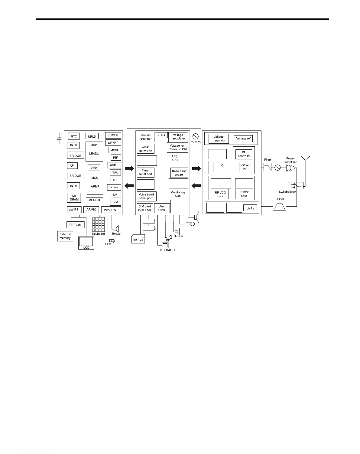
2-1 The RF Chipset
The A316 RF integrates the TRF6150 transceiver IC, TX/RX VCO, Power amplifier(RF3110), Front
End Module 8450T(switchplexer, RF-SAW filter), for dulaband transmitting and receiving function.
32KHz
QUARTZ
VCOs
- 11 -
Page 2
2. TECHNICAL BRIEF
- 12 -
2-1-1 The Receiver
The RF receive signal( EGSM 925Mhz – 960MHz, DCS 1805Mhz – 1880Mhz) is input via the antenna
or coaxial connector.
An antenna matching circuit is between the antenna and the connector.
Page 3
2. TECHNICAL BRIEF
- 13 -
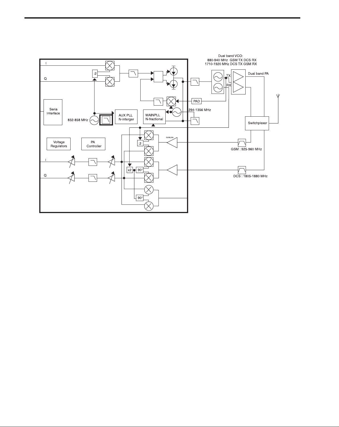
2-1-2 The TX IF Modulator
The TX I & Q signals from baseband IC are fed to Pin#18-21 of the TRF6150, where they are then
modulated onto a TX IF by the modulator inside TRF6150. The TX IF frequency is listed as below.
EGSM Band
DCS Band
The signal TX LO IF (416 ~ 429Mhz) is produced by the AUX VCO (832 ~ 858MHz), which has been
divided down by a factor of 2 .
2-1-3 The Translation Loop Transmitter
The translation loop approach has many advantages over a traditional upconverter solution. A typical
upconverter transmitter usually consists of an IF modulator followed by a mixer for upconversion to RF.
In the translation loop transmitter, the RF transmit signal is instead generated directly by a voltage
controlled oscillator (VCO), the phase of which is locked to the modulated IF reference in a fast phaselocked-loop. Because a VCO is inherently a lower-noise source than a mixer, the translation loop
transmitter produces a low noise floor, so no subsequent high-selectivity filtering is necessary, and the
diplexer or other post-PA filter of the conventional approach is eliminated. This saves power and cost,
as the insertion loss of the duplexer is eliminated, and the output level of the power amplifier can be
reduced.
The transmit signal is generated directly by a external TX/RX VCO (VON1885C28DKB). In the
feedback path, the RF transmit signal is mixed with the off-chip main VCO to produce the desired TXIF
(416 ~ 429Mhz). This TXIF signal from the feedback path is then compared to the TXIF signal from the
IF modulator at the detector. The resulting signal after passing a low pass filter drives the external
TX/RX VCO.
A high side injection, i.e. RF = LO - IF, is used in the EGSM band upconversion while a low side
injection, i.e. RF = LO + IF, is used in the DCS band upconversion. This upconversion scheme, with
appropriate TXIFs, allows for a single wide-band VCO to be used.
From To AUX VCO= 2 x IF Frequency
CH 1 CH 26 858 MHz
CH 27 CH 43 852.8 MHz
CH 44 CH 91 858 MHz
CH 92 CH 108 842.4 MHz
CH 109 CH 985 858 MHz
CH 986 CH 1002 842.4 MHz
CH 1003 CH 1024 858 MHz
From To AUX VCO= 2 x IF Frequency
CH 512 CH 532 832 MHz
CH 533 CH 549 837.2 MHz
CH 550 CH 575 832 MHz
CH 576 CH 597 858 MHz
CH 598 CH 614 837.2 MHz
CH 615 CH 662 858 MHz
CH 663 CH 679 852.8 MHz
CH 680 CH 727 858 MHz
CH 728 CH 744 852.8 MHz
CH 745 CH 792 858 MHz
CH 793 CH 809 847.6 MHz
CH 810 CH 857 858 MHz
CH 858 CH 874 847.6 MHz
CH 875 CH 885 858 MHz
Page 4
2. TECHNICAL BRIEF
- 14 -
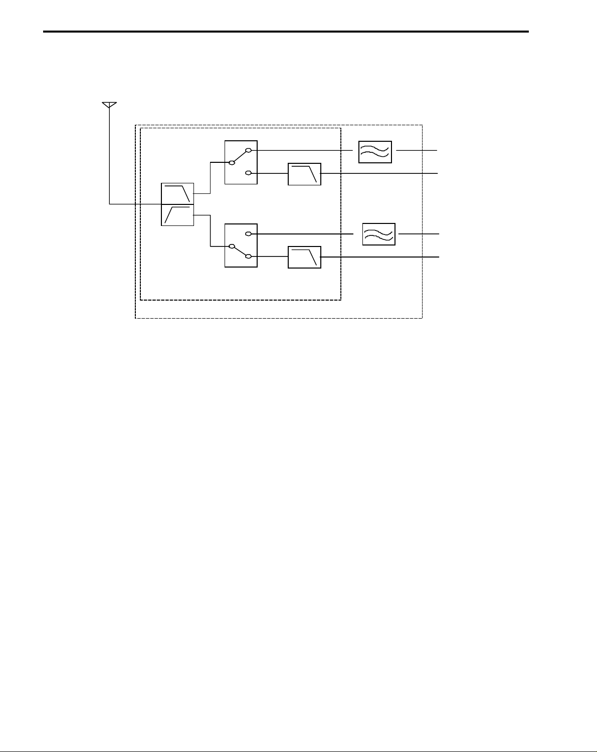
2-2 Front End Module
The switchplexer is used to control the Rx and Tx paths. And the control signals is connected to
Switchplexer(Diplexer) of Front End
Module(FEM8450T) to switch either Rx or Tx path on. When the Rx path is turned on, the RF receive
signal then feeds into two paths, EGSM Rx and DCS1800 Rx.
This Front End Module contains two RF SAW filters, DCS SAW Filter to filter any unwanted signal
apart from the DCS Rx band. And the GSM SAW filter in the Front End Module is to filter out
unwanted signal beyond the GSM Rx band. These two paths are then connected to the GSMLNA and
DCSLNA of TRF6150 respectively.
The RF receive signal is amplified by LNAs in TRF6150, and then the signal then feeds into quadrature
demodulator for mixing with LO which is produced by the main synthesiser of TRF6150 and
external TX/RX VCO. TX/RX VCO will generate 2 times of RX frequency in EGSM band and half times
of RX frequency in DCS band to minimize the DC offset generated by self mixing.
In TRF6150, the quadrature demodulator produce baseband(I/Q) signal . This I/Q signal is amplified by
two variable gain amplifiers and filtered by low pass filter, and then fed to baseband IC in differential
mode.
An t e n n a
An t e n n aAn t e n n a
An t e n n a S w i t c h
Swi tc hSwi tc h
Switch Module
Mo d u l eMo d u l e
Mo d u l e
Diplexer
DiplexerDiplexer
Diplexer
DC S 18 0 0
DC S 18 0 0DC S 1 8 0 0
DC S 18 0 0
Swi tc h
Swi tc hSwi tc h
Swi tc h
EG S M
EG S MEG S M
EG S M
Swi tc h
Swi tc hSwi tc h
Swi tc h
LPF
LPFLPF
LPF
LPF
LPFLPF
LPF
An t
An tAn t
An t
DC S 18 0 0
DC S 18 0 0DC S 1 8 0 0
DC S 18 0 0
band
bandband
band
EG S M
EG S MEG S M
EG S M ba n d
bandband
band
EGSM-Rx
EGSM-RxEGSM-Rx
EGSM-Rx
EGSM-Tx
EGSM-TxEGSM-Tx
EGSM-Tx
DCS1800-Rx
DCS1800-RxDCS1800-Rx
DCS1800-Rx
DCS1800-Tx
DCS1800-TxDCS1800-Tx
DCS1800-Tx
SAW
SAWSAW
SAW
SAW
SAWSAW
SAW
Fro nt
Fro ntFro nt
Fro nt End
En dEn d
En d Mod ul e
Mo d u l eMo d u l e
Mo d u l e
Page 5
2. TECHNICAL BRIEF
- 15 -
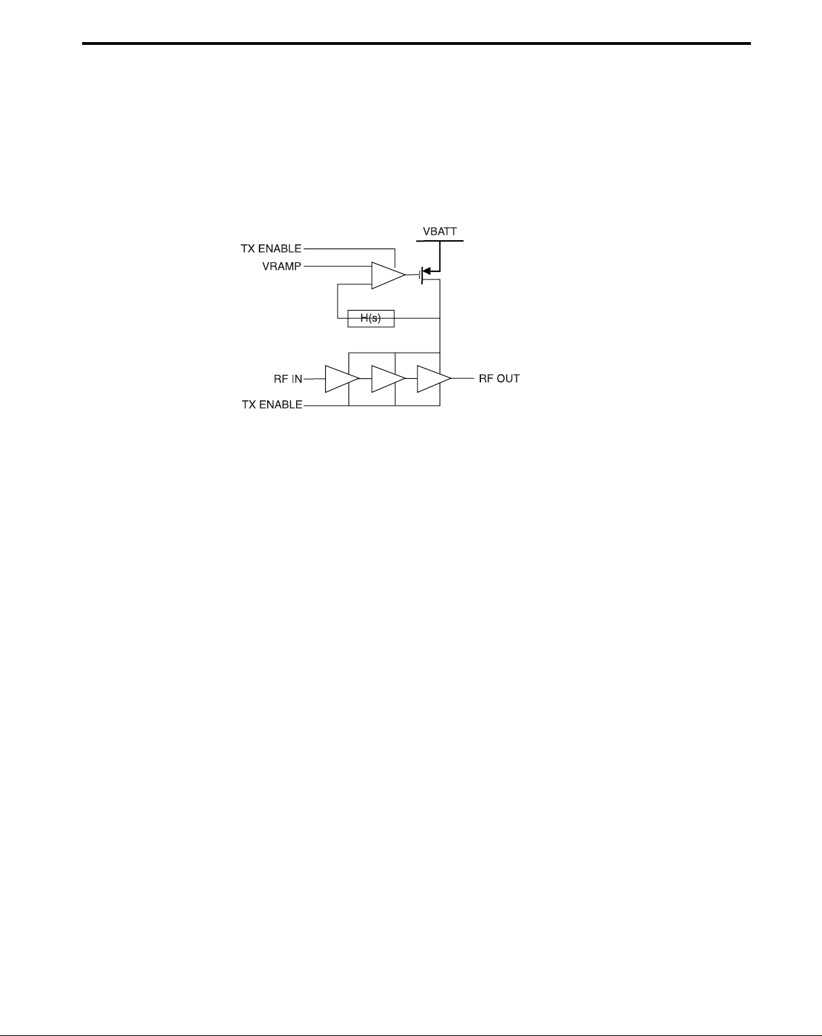
2-3 The PA Circuit
The RF3110 is a triple-band GSM/DCS/PCS power amplifier module that incorporates an indirect
closed loop method of power control. This simplifies the phone design by eliminating the need for the
complicated control loop design. The indirect closed loop is fully self contained and required does not
require loop optimization. It can be driven directly from the DAC out-put in the baseband circuit.
The indirect closed loop is essentially a closed loop method of power control that is invisible to the
user. Most power control systems in GSM sense either for-ward power or collector/drain current. The
RF3110 does not use a power detector. A high-speed control loop is incorporated to regulate the
collector voltages of the amplifier while the stages are held at a constant bias. The V RAMP signal is
multiplied and the collector voltages are regulated to the multiplied V RAMP voltage.
Page 6

2. TECHNICAL BRIEF
- 16 -
2-4 Penpheral Citcult
Temperature Sensor
When the chip is not transmitting or receiving, its temperature can be measured by sensing the
voltage on the external resistor from pin 31 to ground. From –40 to +85 C, the resistor voltage
varies linearly from 0.9V to 1.35V.
Regulator and Serial Data Interface
TRF6150 built in 3 voltage regulators to supply internal functions and external RF components.
The serial interface of TRF6150 consists of a 3-wire serial bus, comprising DATA, CLOCK and
STROBE signals. These signals are used to enter control words into the chip. The control words
contain information for programming the regulators, the synthesizers and the receiver.
13 MHz Clock
The 13 MHz-clock consists of a TCXO (TOA1300VPM4DKG-SM2) which oscillates at a
frequency of 13MHz. It acts as time base of all synthesizers and Baseband.
2-5 Digital Baseband Chip : HERCROM20, F741529
HERCROM20 is a chip implementing the digital baseband processing of a GSM mobile phone. It
combines a TMS320C54X (LEAD2) DSP, a micro controller ARM7TDMIE, an internal 2Mbit RAM
memory, and their associated application peripherals.
The HERCROM20 supports the following features:
• CPU & DSP
• Memory Interface (MEMINT)
• Interrupt Controller
• I2C / Micro Wire Interface
• Serial Port Interface (SPI)
• UART Control/Interface
• Display Interface
• SIM Card Interface
• I/O System Connector Interface
• Radio Interface (RIF)
• JTAG Interface
• Real Time Clock (RTC)
• General Timers / Watch Dog Timer
• Keypad Control
• Backlight Control
• Vibrator Control
Page 7

2. TECHNICAL BRIEF
- 17 -
System Block Diagram of Hercrom20
Page 8

2. TECHNICAL BRIEF
- 18 -
2-6 Analog Baseband Chip : Nausica_CS, TWL3012B
The TWL3012B device includes a complete set of baseband functions that perform the interface and
processing of the following, voice signals, the baseband in-phase (I) and the quadrature (Q) signals,
which support both the single-slot and multislot modes. The TWL3012B device also includes
associated auxiliary RF control features, supply voltage regulation, battery charging controls, and
switch on/off system analysis.
The TWL3012B device supports the following features.
• Voiceband Coder / Decoder (codec)
• Baseband codec single and multislot with I/Q RF interface
• Automatic Power Control(APC) and Automatic Frequency Control (AFC)
• Voiceband Serial Port (VSP), Baseband Serial Port (BSP), and MCU Serial Port(USP),
Timing Serial Port(TSP).
• SIM Card Interface
• Battery Charging Interface (BCI)
• Six Low-Dropout, Low-Noise, Linear Voltage Regulators (VREG)
• Voltage Reference and Power On Control (VRPC)
• Five-channel analog-to-digital converter (MADC)
Page 9

2. TECHNICAL BRIEF
- 19 -
System Block Diagram of Nausica_CS
Page 10

2. TECHNICAL BRIEF
- 20 -
2-7 CPU Memories
Flash ROM
An 16Mbit programmable ROM which is capable of being written to while still in circuit. Contains all the
main command software for the mobile.
SRAM
A 2MBit SRAM memory is embedded in the HERCROM20 which is used for ARM7 & DSP execution.
2-8 Power Supplies
There are six regulators in the Nausica_CS . Those regulators are dedicated power supplies, which
provides most of the power requirements for the Baseband and RF circuits. Each of these regulators
can be controlled by Nausica_CS internal registers. These are configured as shown in the following
Figure and table .
Table1. – Power Supply
Regulator Voltage Powers Permanent
Regulator VR1 1.8V+/-0.15 Digital Core & RTC Permanent
Regulator 1B VR1B 2.0V+/-0.2 Nausica_CS Internal logic On/Off
Regulator VR2 2.9V+/-0.1 Memory device Permanent
Regulator VR2B 2.85V+/-0.15 Peripheral Permanent
Regulator VR3 2.85V+/-0.15 Nausica _CS analog supply ON/Off
SIM Regulator 3V+/-0.35V+/-0.5 SIM Card On/Off
Page 11

2. TECHNICAL BRIEF
- 21 -
Figure 1. Power supply
Page 12

2. TECHNICAL BRIEF
- 22 -
2-9 Battery Charge Interface
The charging device is a dc voltage source of 7 V absolute maximum. An external PMOS power
transistor in series with a power Schottky diode connected between VCHG and VCC3 of the
TWL3012B device controls the current flow from the charging device to the main battery. The role of
the Schottky diode is to prevent reverse leakage current from the main battery in case the charging
device is connected to the mobile phone without delivering any voltage at its output (charging device
not plugged into the ac wall outlet, for example).
The main function of the battery charger interface is the charging control of both Ni-MH/Ni-Cd/Li-Ion
cell battery with the support of the microcontroller. In case of a rechargeable backup battery, it also
delivers a trickle charge current to the backup battery from the main battery. The charging scheme for
the Li-Ion battery is constant current first (typical current is 1xC) followed by constant voltage charging
once a certain voltage threshold is reached (4.2 V typical). Charging is stopped when the charging
current at constant voltage has decreased down to C/20 (typical).
In addition to the above charging schemes, another scheme is systematically applied when a battery
charger is connected to a switched-off mobile phone: a constant charging current (typically C/20) is
applied to the battery when the battery voltage is lower than 3.6 V.
If the battery voltage is lower than 3.2 V (battery partially discharged or fully discharged) the mobile
phone is not started until the battery gets sufficiently recharged to greater than 3.2 V; when this
happens, the micro-controller is started to control the fast charge cycle of the main battery, and the
C/20 current is switched off.
Page 13

2. TECHNICAL BRIEF
- 23 -
Battery Charge Control Circuit
Page 14

2. TECHNICAL BRIEF
- 24 -
2-10 System Connector
This Phone is equipped with a LG standard system connector MQ203-GVA-16R-PWJ for travel/desk
charger, accessories connection and data access (trace•debug and SW download).
System Connector Specification
Pin Name Description I /O
1 DGND Digital ground. In / Out
2
3 DC_In DC input for Charger. ( 5V / 650mA ) In
4
5 HF_Det Headset/HandsFree car-kit detection. In
6 DC_Out DC output for External accessories. ( 3V / 200 mA ) Out
7 RXD1 Primary serial data in. In
8 TXD1 Primary serial data out. Out
9 Mute (DTR) MS off-hook indicator. Active high. Out
10 RXD2 (DCD) Secondary serial data in. In
11 CTS Clear to Send. In
12 RTS Request to send. Out
13 Audio_Out Audio output. Out
14 Vflash / On_Req Vpp for flash memory. ( 12V / 25 mA ) / MS On request. In / In
15 Audio_In Audio input / Off_Hook detection for advanced headset. In
16 AGND Analog ground. In / Out
17 TXD2 Secondary serial data out. Out
18 DGND Digital ground. In / Out
Page 15

2. TECHNICAL BRIEF
- 25 -
2-11 Keypad Switches and Scanning
The key switches are metal domes which make contact between two concentric pads on the top layer
of the PCB when pressed. There are 18 switches (S301-318), connected in a matrix of 5 rows by 4
columns, as shown in Figure, except for the power switch(S313) which is connected independently.
Functions, the row and column lines of the keypad are connected to ports of Hercrom20. The rows are
outputs with pull-up resistors embedded in chipset, while the columns are inputs. When a key is
pressed, the corresponding row and column are connected together, causing the row output to go low
and generate an interrupt. The columns/rows are then scanned by Hercrom20 to identify the pressed
key.
Page 16

2. TECHNICAL BRIEF
- 26 -
2-12 Display Interface
Power to the LCD is supplied by VR2B of Nausica_CS. The LCD can be reseted by RES. A low on this
output reset the LCD. There is also the control output CS which is also derived from Hercrom20, this
acts as the chip select enable for the LCD module. Hercrom20 uses data line D0-D7 to send serial data
for displaying graphical text onto the LCD.
Page 17

2. TECHNICAL BRIEF
- 27 -
2-13 Microphone
A microphone holder is mounted on PCB and is used to hold the microphone between frond cover and
PCB. The audio signal is passed to the MICIN of Nausica_CS. The voltage supply MICBIAS is coming
from Nausica_CS., and is a bias voltage for both the MICIP and AUDIO_IN lines form system
connector. The MICIN and AUDIO_IN signal is then A/D converted by the voiceband codec of
Nausica_CS. The digitized speech is then passed to the DSP of Hercrom20 for processing (coding,
interleaving etc.).
2-14 Receiver/Speaker/Buzzer
The low impedance speaker is driven by an audio amplifier. The audio amplifier is controlled by the
SHUTDOWN pin form Hercrom20. In normal off-hook, the audio amplifier is turned on, when the
headset is plugged in , the audio amplifier is turned off. When on-hook, the audio amplifier is turned off
for power saving. There are two audio path (EARP & AUXOP) coming from Nausica_CS. In Receiver
mode, the audio input is fed with EARP, In Speaker/Buzzer mode, the audio input is fed with AUXOP.
Page 18

2. TECHNICAL BRIEF
- 28 -
2-15 Headset Interface
The audio input of the headset is connected to AUXIN pin of Nausica_CS, the microphone is biased by
MICBIAS pin form Nausica_CS, too.
The audio out to the headset kit is fed with EARN pin of Nausica_CS,
2-16 Back-light Illumination
In Back-Light illumination, there are 10 green LEDs (six for keys and four for the LCD), which are
driven by BACKLIGH line from Hercrom20. The purpose of Q302A, R319 and R318 is used for the
indication of pre-charge.
Page 19

2. TECHNICAL BRIEF
- 29 -
2-17 Vibrator
The vibrator is driven by the signal VIBRATOR, which is output from Hercrom20. The signal is
amplified by the transistor Q301A (IMX9) and is supplied from Vbat.
 Loading...