

LG CD-962A, AX Service manual
4
SERVICING PRECAUTIONS
NOTES REGARDING HANDLING OF THE PICK-UP
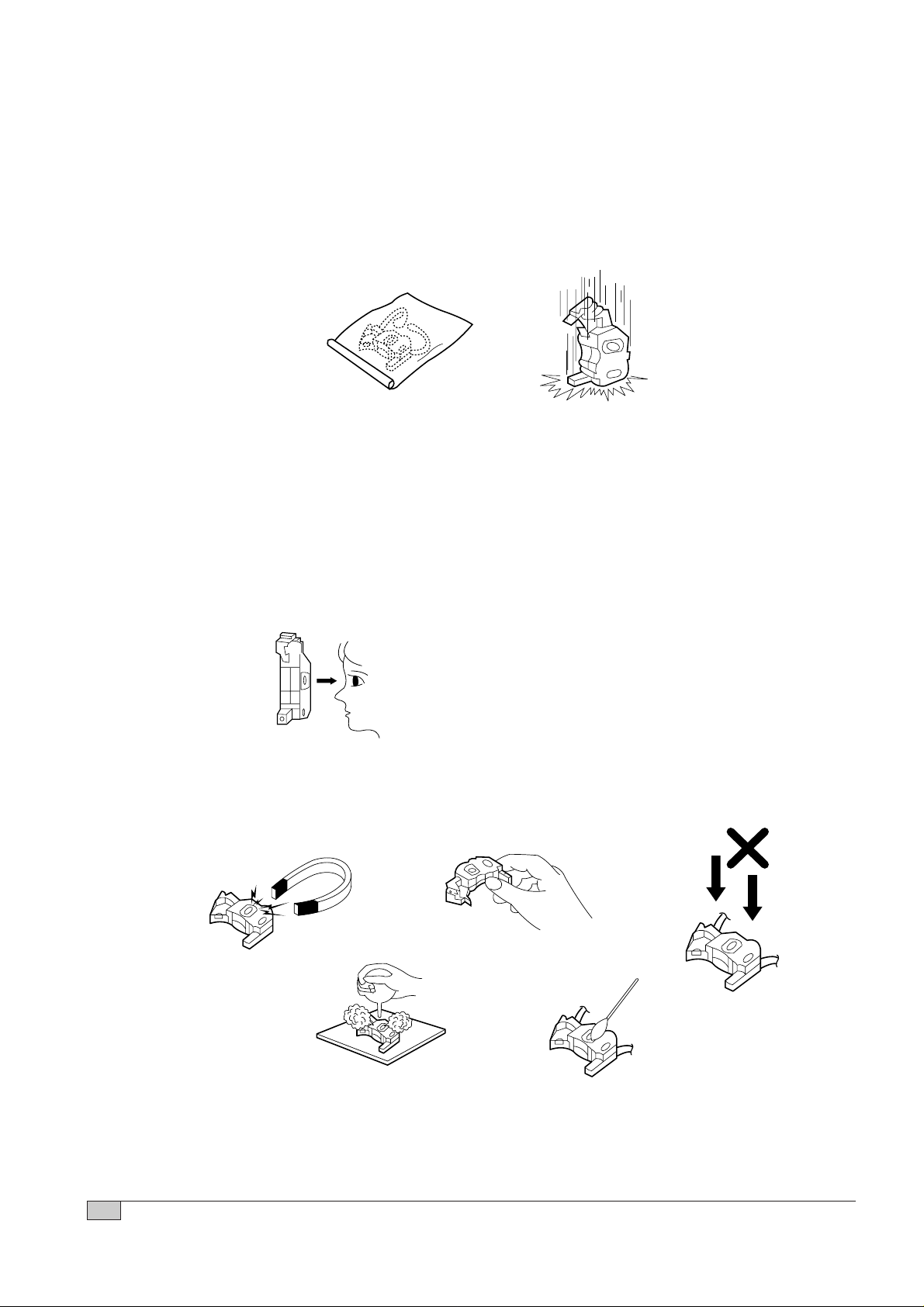
1. Notes for transport and storage
1) The pick-up should always be left in its conductive bag until immediately prior to use.
2) The pick-up should never be subjected to external pressure or impact.
2. Repair notes
1) The pick-up incorporates a strong magnet, and so should never be brought close to magnetic materials.
2) The pick-up should always be handled correctly and carefully, taking care to avoid external pressure and
impact. If it is subjected to strong pressure or impact, the result may be an operational malfunction and/or
damage to the printed-circuit board.
3) Each and every pick-up is already individually adjusted to a high degree of precision, and for that reason
the adjustment point and installation screws should absolutely never be touched.
4) Laser beams may damage the eyes!
Absolutely never permit laser beams to enter the eyes!
Also NEVER switch ON the power to the laser output part (lens, etc.) of the pick-up if it is damaged.
5) Cleaning the lens surface
If there is dust on the lens surface, the dust should be cleaned away by using an air bush (such as used
for camera lens). The lens is held by a delicate spring. When cleaning the lens surface, therefore, a
cotton swab should be used, taking care not to distort this.
6) Never attempt to disassemble the pick-up.
Spring by excess pressure. If the lens is extremely dirty, apply isopropyl alcohol to the cotton swab. (Do
not use any other liquid cleaners, because they will damage the lens.) Take care not to use too much of
this alcohol on the swab, and do not allow the alcohol to get inside the pick-up.
Storage in conductive bag
Drop impact
NEVER look directly at the laser beam, and don
¡˙t let
contact fingers or other exposed skin.
Magnet
How to hold the pick-up
Pressure
Pressure
Cotton swab
Conductive Sheet
5
NOTES REGARDING COMPACT DISC PLAYER REPAIRS
1. Preparations
1) Compact disc players incorporate a great many ICs as well as the pick-up (laser diode). These
components are sensitive to, and easily affected by, static electricity. If such static electricity is high
voltage, components can be damaged, and for that reason components should be handled with care.
2) The pick-up is composed of many optical components and other high-precision components. Care must
be taken, therefore, to avoid repair or storage where the temperature of humidity is high, where strong
magnetism is present, or where there is excessive dust.
2. Notes for repair
1) Before replacing a component part, first disconnect the power supply lead wire from the unit
2) All equipment, measuring instruments and tools must be grounded.
3) The workbench should be covered with a conductive sheet and grounded.
When removing the laser pick-up from its conductive bag, do not place the pick-up on the bag. (This is
because there is the possibility of damage by static electricity.)
4) To prevent AC leakage, the metal part of the soldering iron should be grounded.
5) Workers should be grounded by an armband (1MΩ)
6) Care should be taken not to permit the laser pick-up to come in contact with clothing, in order to prevent
static electricity changes in the clothing to escape from the armband.
7) The laser beam from the pick-up should NEVER be directly facing the eyes or bare skin.
Armband
Conductive
Sheet
Resistor
(1 Mohm)
Resistor
(1 Mohm)

6
ESD PRECAUTIONS
Electrostatically Sensitive Devices (ESD)
Some semiconductor (solid state) devices can be damaged easily by static electricity. Such components
commonly are called Electrostatically Sensitive Devices (ESD). Examples of typical ESD devices are integrated
circuits and some field-effect transistors and semiconductor chip components. The following techniques should
be used to help reduce the incidence of component damage caused by static electricity.
1. Immediately before handling any semiconductor component or semiconductor-equipped assembly, drain off
any electrostatic charge on your body by touching a known earth ground. Alternatively, obtain and wear a
commercially available discharging wrist strap device, which should be removed for potential shock reasons
prior to applying power to the unit under test.
2. After removing an electrical assembly equipped with ESD devices, place the assembly on a conductive
surface such as aluminum foil, to prevent electrostatic charge buildup or exposure of the assembly.
3. Use only a grounded-tip soldering iron to solder or unsolder ESD devices.
4. Use only an anti-static solder removal device. Some solder removal devices not classified as "anti-static" can
generate electrical charges sufficient to damage ESD devices.
5. Do not use freon-propelled chemicals. These can generate electrical charges sufficient to damage ESD
devices.
6. Do not remove a replacement ESD device from its protective package until immediately before you are
ready to install it. (Most replacement ESD devices are packaged with leads electrically shorted together by
conductive foam, aluminum foil or comparable conductive materials).
7. Immediately before removing the protective material from the leads of a replacement ESD device, touch the
protective material to the chassis or circuit assembly into which the device will by installed.
CAUTION : BE SURE NO POWER IS APPLIED TO THE CHASSIS OR CIRCUIT, AND OBSERVE ALL OTHER
SAFETY PRECAUTIONS.
8. Minimize bodily motions when handing unpackaged replacement ESD devices. (Otherwise harmless motion
such as the brushing together of your clothes fabric or the lifting of your foot from a carpeted floor can
generate static electricity sufficient to damage an ESD device).
8
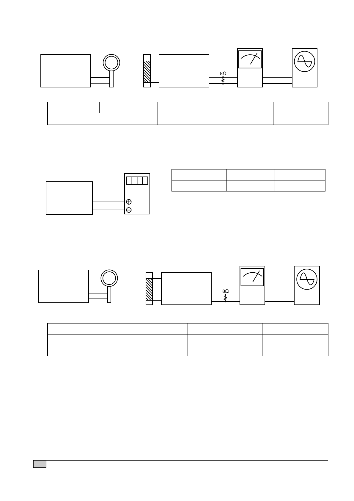
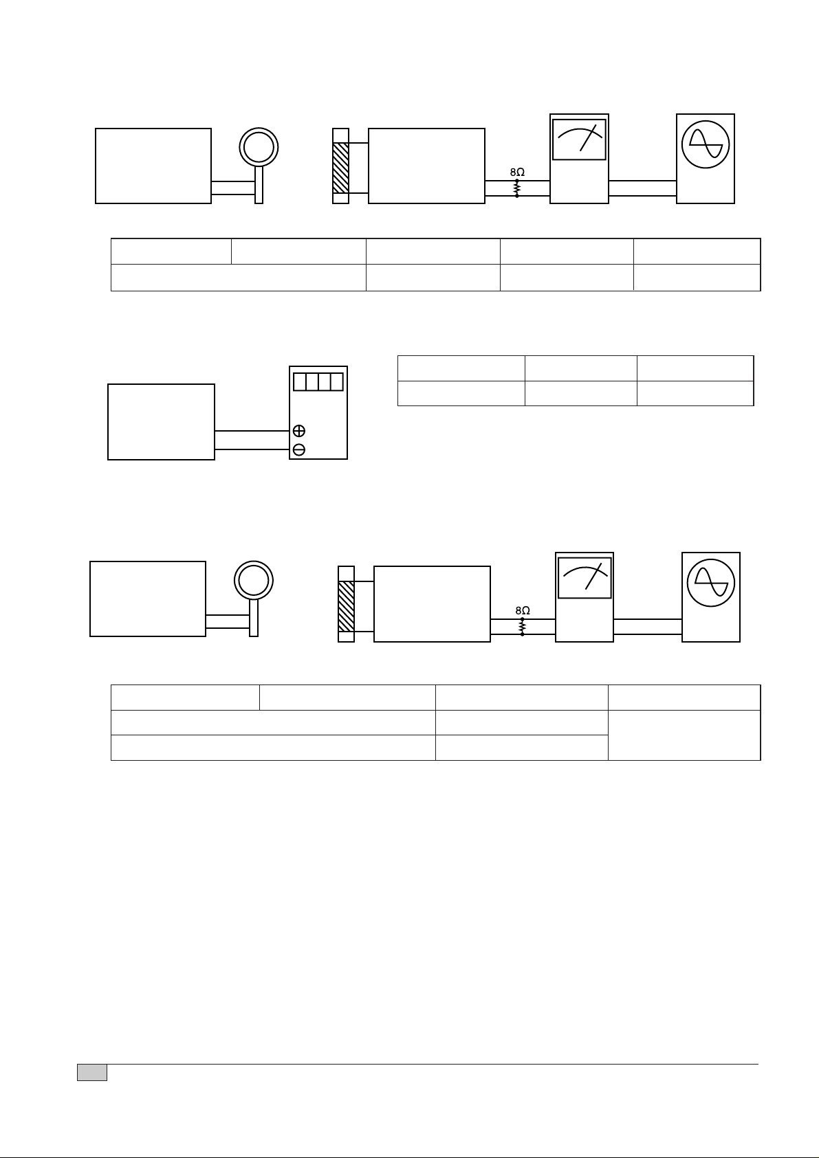
2. AM IF Adjustment
Figure 4.
4. AM Tracking Adjustment
Figure 3.
3. AM Coverage Adjustment
Figure 2.
Loop Ant.
SSG SET
L71
VTVM
OSCILLOSCOPE
Terminal
GND
Output
VOLTMETER
SET
PIN 2
GND
Loop Ant.
SSG
SETL71
VTVM
OSCILLOSCOPE
Terminal
GND
Output
SET Frequency Adjustment Adjustment
522kHz(9kHz Step) L72 1.0V ± 0.05V
SSG Frequency SET Frequency Adjusting part Adjustment Remark
1008kHz(9kHz Step)
T2 450kHz±1kHz Maximize the output
SSG Frequency SET Frequency Adjusting part Adjustment
603kHz(9kHz Step) L71
1404kHz(9kHz Step) TC71
Maximize the output
9
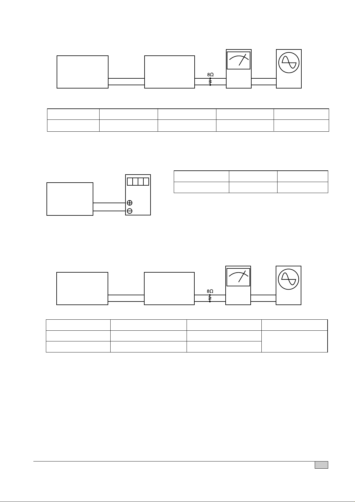
Figure 5.
5. FM IF Adjustment
6. FM Coverage Adjustment
Figure 7.
7. FM Tracking Adjustment
Figure 6.
VOLTMETER
SET
PIN 2
GND
SSG
SET
VTVM
OSCILLOSCOPE
Terminal
GND
PIN1
GND
Output
SSG
SET
VTVM
OSCILLOSCOPE
Terminal
GND
PIN1
GND
Output
SSG Frequency SET Frequency Adjusting part Adjustment Remark
90MHz 90MHz T1 10.7MHz Maximize the output
SET Frequency Adjusting Part Adjustment
76MHz L2 1 ± 0.05V
SSG Frequency SET Frequency Adjusting part Adjustment
78.6MHz 78.6MHz L1
101.75MHz 101.75MHz TC1
Maximize the output
10
10. LW IF Adjustment
Figure 12.
12. LW Tracking Adjustment
Figure 11.
11. LW Coverage Adjustment
Figure 10.
Loop Ant.
SSG SET
L71
VTVM
OSCILLOSCOPE
Terminal
GND
Output
VOLTMETER
SET
PIN 2
GND
Loop Ant.
SSG
SETL71
VTVM
OSCILLOSCOPE
Terminal
GND
Output
SET Frequency Adjustment Adjustment
153kHz L82 1.3 ± 0.05V
SSG Frequency SET Frequency Adjusting part Adjustment Remark
999kHz(9kHz Step), 1000kHz(10kHz Step) T2 450kHz±1kHz Maximize the output
SSG Frequency SET Frequency Adjusting part Adjustment
164kHz L71
254kHz TC81
Maximize the output
11
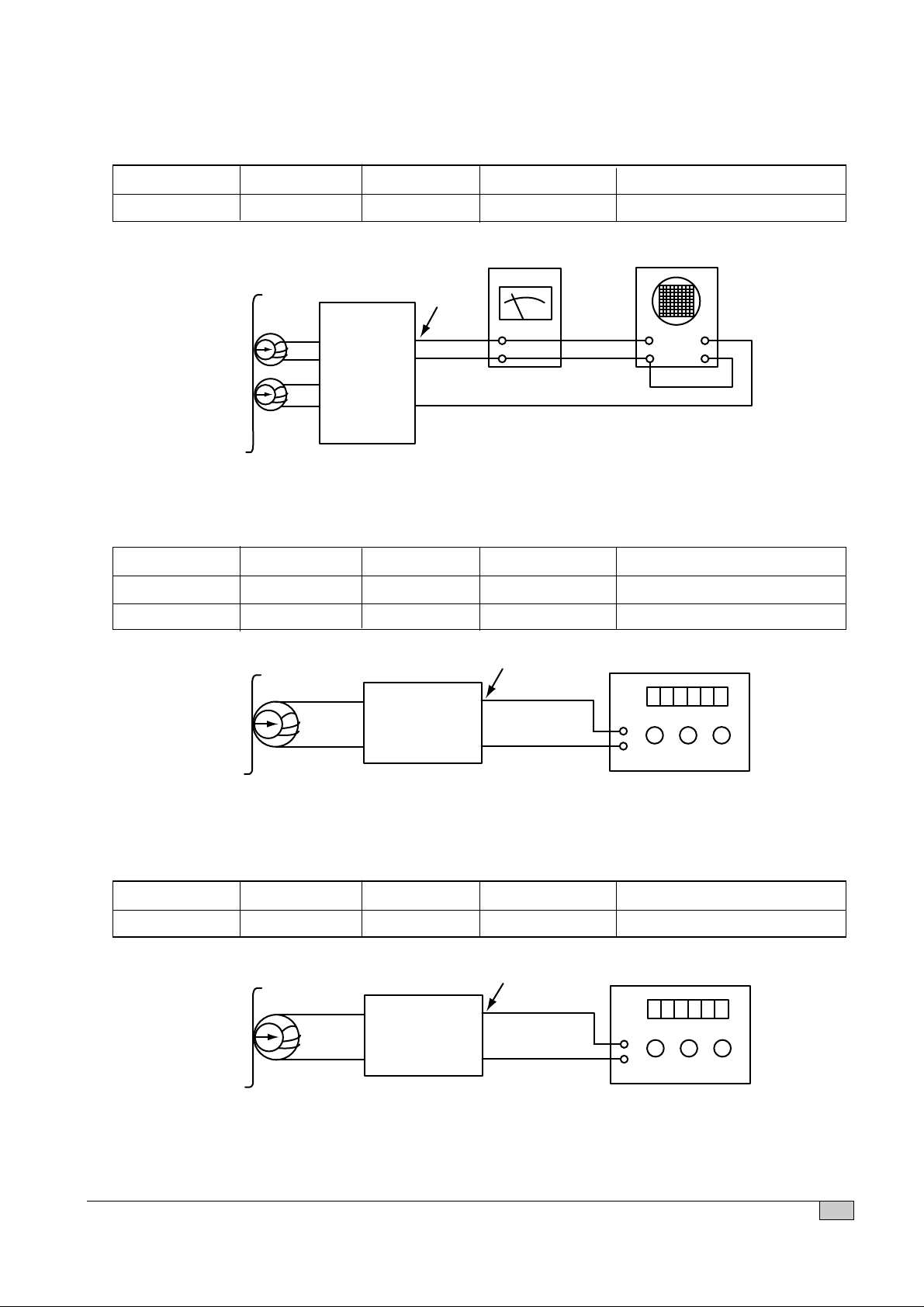
TAPE DECK ADJUSTMENT
1. AZIMUTH ADJUSTMENT
Figure 2. Azimuth Adjustment Connection Diagram
2. MOTOR SPEED ADJUSTMENT
Figure 3. Motor Speed Adjustment Connection Diagram
3. RECORD BIAS ADJUSTMENT
Figure 4. Record Bias Adjustment Connection Diagram
CH1 CH2
Speaker Out
Playback Mode
Head
Test Tape
MTT-114
L ch
R ch
GND
Dual-trace
synchroscope
Electronic
Voltmeter
L out
R out
Unit
Head
Playback Mode
Unit
Speaker Out
GND
L out
R out
Record/Playback
head
Test Tape
MTT-111
Frequency Counter
Deck Mode Test Tape Test Point Adjust for Adjustment
Playback MTT-114 L/R Output R/L Maximum Azimuth adjusting screw
Deck Mode Test Tape Test Point Adjust for Adjustment
Rec/Pause MTT-5511 Q140 EMITTER 70kHz±800Hz L140
Deck Mode Test Tape Test Point Adjust for Adjustment
Playback MTT-111N L/R Output 3kHz±90Hz VR250
Playback MTT-111N L/R Output 5.4kHz~6.3kHz CONFIRM
Test Tape
MTT-5511
Head
Record/Playback
and Pause Mode
Unit
PN102
Frequency Counter
Record/Playback
head
GND
13
CDP ADJUSTMENTS
When change the pick-up must be confirm as follow
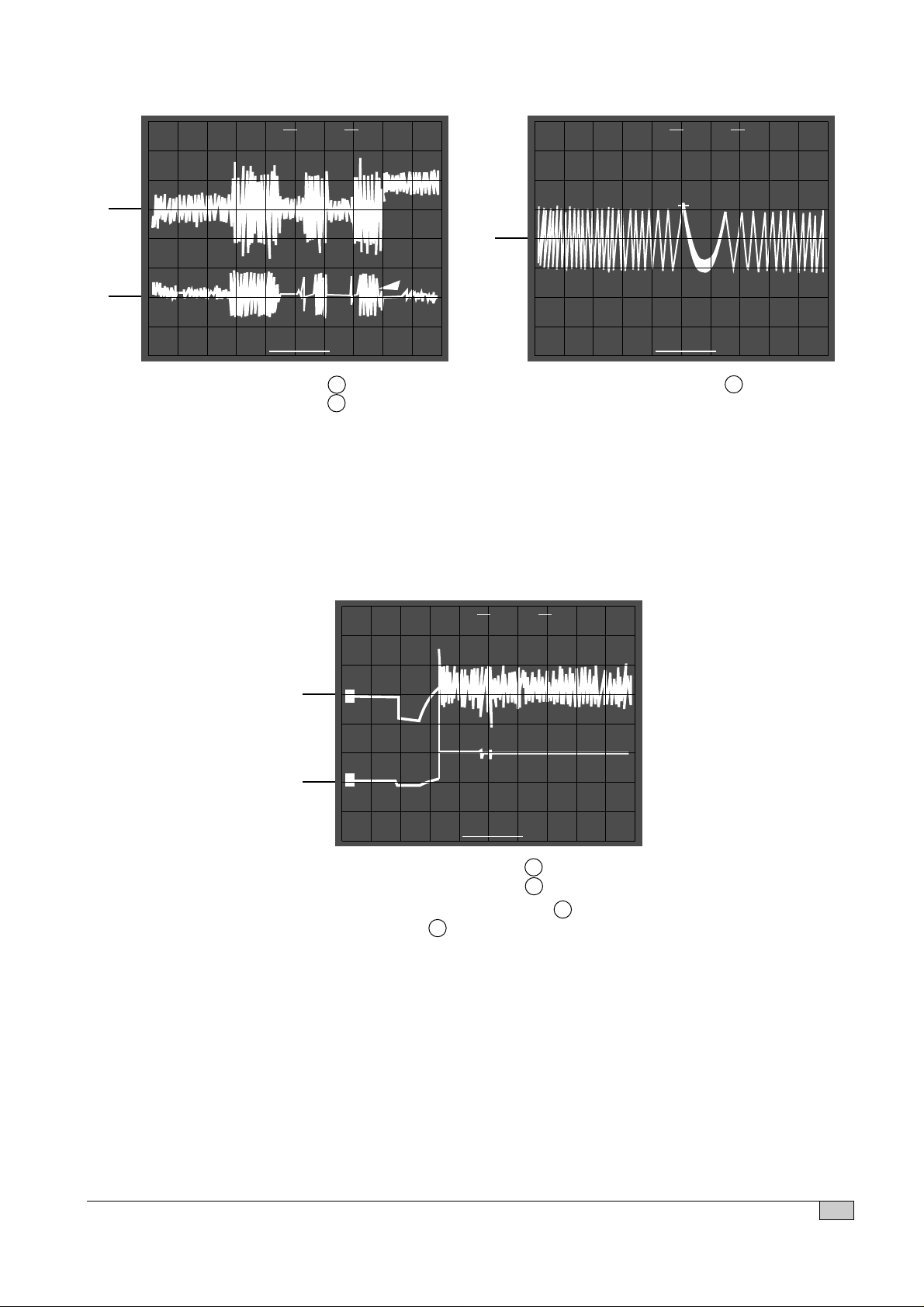
1. TRACKING BALANCE CONFIRMATION
1. Connect the oscilloscope to TEO and REF.
2. Access from 1 st selection to last section of test disc (YEDS-18)
3. Confirm the normal state of tracking error signal (T.B deviation : less than ±3%)
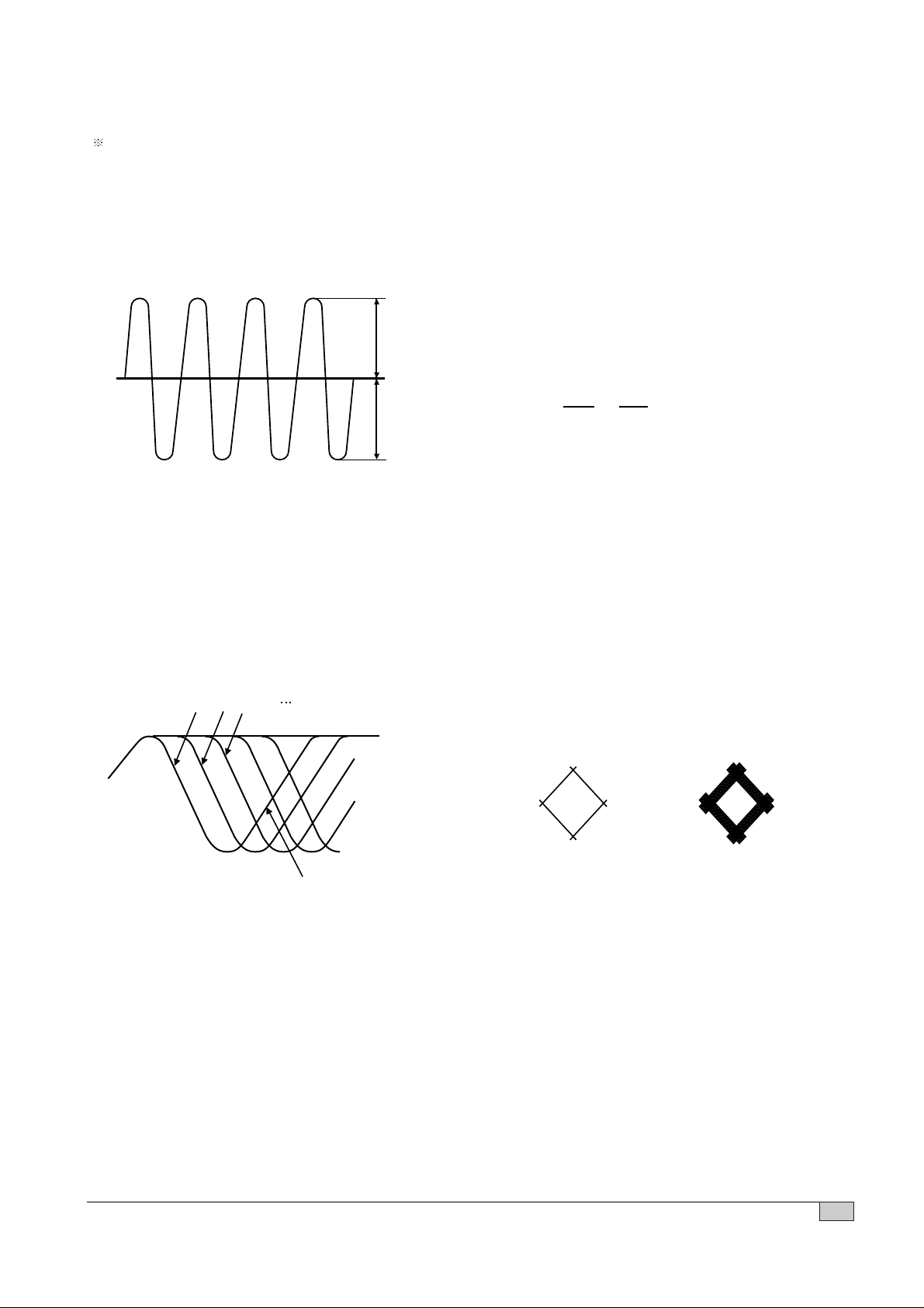
2. RF WAVEFORM CONFIRMATION
1. Connect the oscilloscope to RF and REF.
2. Put a test disc (SONY YEDS-18) into unit and playback the 18th selection of the test disc.
3. Confirm the normal state of RF waveform.
4. Confirm the less than 30nS of Jitter Meter reading.
OV(DC Mode) T.B deviation(%)
= X %
A
B
A=B
A+B
A-B
2
100
3T, 4T 5T,6T 11T
EYE-PATTERN EYE-PATTERN
OK NG
14
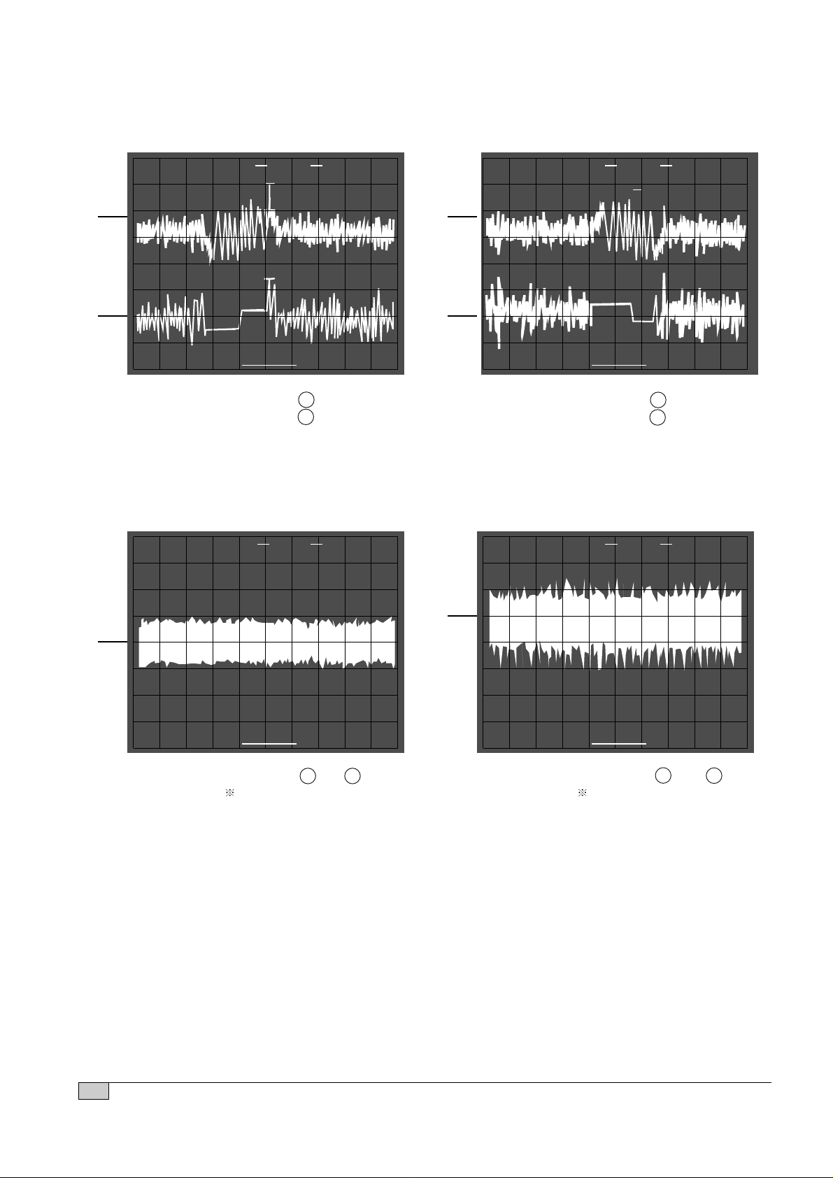
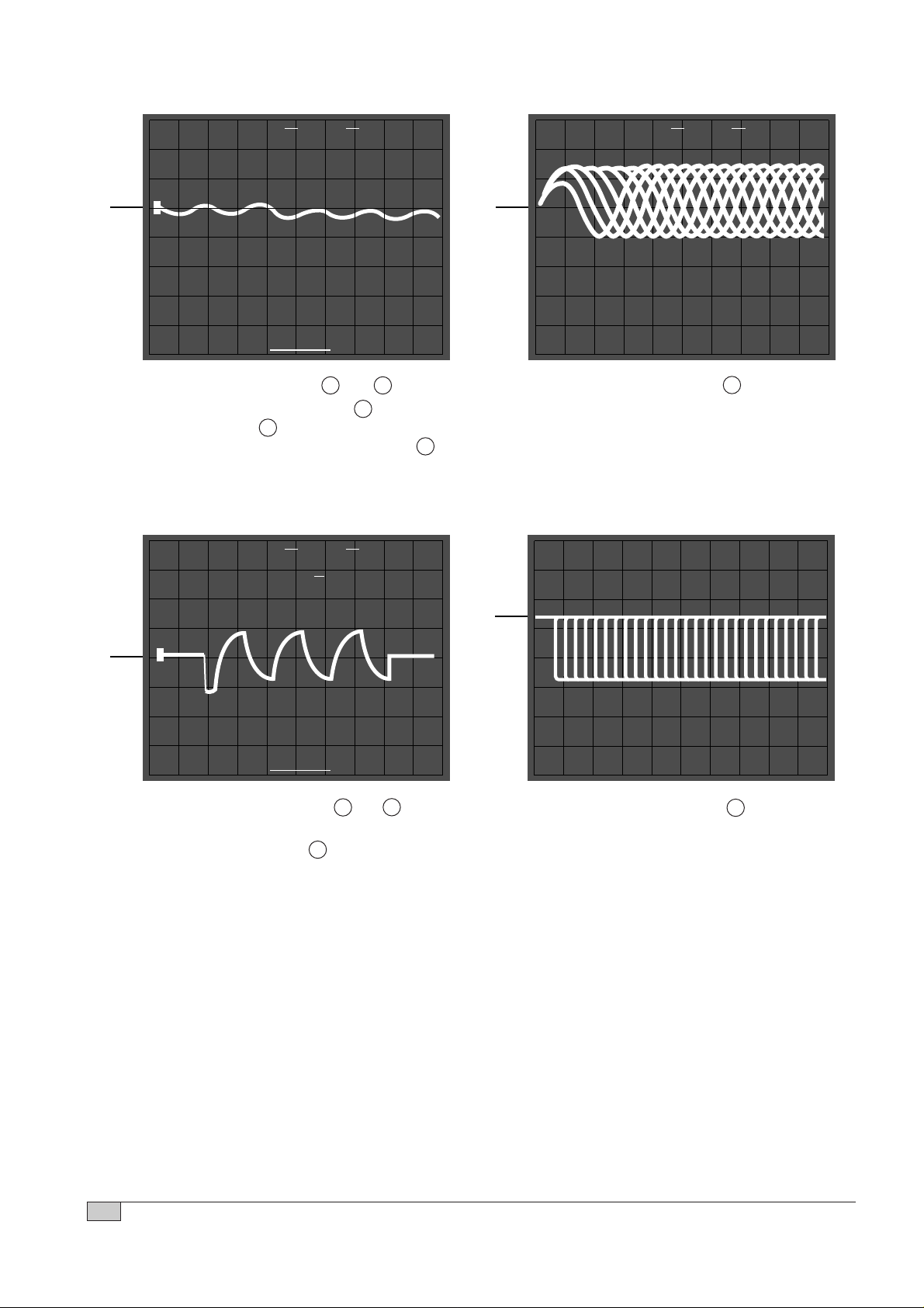
• Connection : 1. IC501 pin 54.(TEO)
2. IC501 pin 50
• Inspection : Check tracking servo
circuit.(RWD)
• Connection : 1. IC501 pin 54 .(TEO)
2. IC501 pin 50
• Inspection : Check tracking servo
circuit.(FWD)
FOCUS GAIN TRACKING GAIN
• Connection : 3. IC502 pin 1 and 2 .
Test disc : YEDS-43
• Inspection : Check focus servo circuit.
• Connection : 3. IC502 pin 26 and 27
Test disc: YEDS-43
• Inspection : Check tracking servo
circuit.
TRACKING ERROR(REW) TRACKING ERROR(FWD)
MAJOR WAVEFORM
∆V1=0.00V TRIG 1=1.0V
∆V2=0.00V
DLY>=0.85ms
1V 1V PEAKDET 1ms 1ms
SAVE
∆T=0.00ms
∆V1=0.00V TRIG 2=1.0V
∆V2=0.00V SREF 2 A
DLY>=0.85ms
1V 1V PEAKDET 1ms 1ms
∆T=0.00ms
∆V1=0.000V TRIG 1=0.09V
DLY>=4.25ms
0.5V PEAKDET 5ms 5ms
SAVE
∆T=0.00ms
∆V1=0.0% TRIG 1=-82%
DLY>=0.170s
>1V PEAKDET 0.2s 50ms
SAVE
∆T=0.000s
1
2
3
4
1
2
15
TRACKING COIL DRIVE E.F. BALANCE
• Connection : 1. IC501 pin 54 . (TEO)
2. IC501 pin 50
• Inspection : - Confirm tracking servo circuit.
- Check IC501 (Cold solder joint
or short circuit)
• Connection : 1. IC501 pin 54 .
• Inspection : Confirm tacking servo balance
deviation rate
READING
• Connection : 7. IC501 pin 48 .
8. IC501 pin 40 (FOK)
• Inspection : Check IC501 pin 4 to IC501 pin
48 (Pattern defective)
∆V1=0.00V TRIG 1=-0.1V
∆V2=0.00V
DLY>=0.425s
1V 2V PEAKDET 0.5s 50ms
SAVE
∆T=0.000s
∆V1=3.96V TRIG 1=1.1V
DLY>=1.70ms
1V PEAKDET 2ms 2ms
SAVE
∆T=0.00ms
∆V1=0.00V TRIG 1=0.2V
∆V2=0.00V
DLY>=0.425s
2V 5V PEAKDET 0.5s 50ms
SAVE
∆T=0.000s
1
1
2
7
8
16
• Connection : 9. IC502 pin 17 and 18
• Inspection : - Check IC501 pin 43 to IC502
pin 20 (Pattern defective)
- Check voltage. (IC502 pin 20 )
• Connection : 10. IC501 pin 74 .
• Inspection : Check objective Lens of Pickup
clear or not
• Connection : 11. IC502 pin 1 and 2 .
• Inspection : - Is focus search signal output to
IC501 pin 48 ?
• Connection : 12. IC501 pin 33 .
• Inspection : Check IC503 and surrounding
circuit (Cold solder joint or short
circuit)
TRIG 1=1.1V
∆V2=0.000V
DLY>=0.085s
0.5V PEAKDET 0.1s 50ms
SAVE
∆T=0.000s
TRIG 1=24%
DLY>=0.670ms
50mV 0.5ms 0.5ms
∆V1=0.00V TRIG 1=0.3V
DLY>=0.085s
2V PEAKDET 1s 50ms
SAVESREF 3 A
∆T=0.00s
>2V
9
11
12
10
 Loading...