

LG ACC-55-R, ACC-55-T, LHW-551-TB Service manual

WIRELESS DVD RECEIVER
SERVICE MANUAL
MODEL : LH-W551TB
LHS-55TBC, LHS-55TBS,
LHS-55TBW,
ACC55T, ACC55R
MODEL : LH-W551TB LHS-55TBC, LHS-55TBS, LHS-55TBW, ACC55T, ACC55R
SERVICE MANUAL

1-1
[CONTENTS]
SECTION 1. GENERAL
• SERVICING PRECAUTIONS . . . . . . . . . . . . . . . . . . . . . . . . . . . . . . . . . . . . . . . . . . . . . . . 1-2
• ESD PRECAUTIONS . . . . . . . . . . . . . . . . . . . . . . . . . . . . . . . . . . . . . . . . . . . . . . . . . . . . 1-4
• SPECIFICATIONS . . . . . . . . . . . . . . . . . . . . . . . . . . . . . . . . . . . . . . . . . . . . . . . . . . . . . . . .1-5
SECTION 2. AUDIO PART
• AUDIO TROUBLESHOOTING GUIDE . . . . . . . . . . . . . . . . . . . . . . . . . . . . . . . . . . . . . . . . 2-1
• WIRING DIAGRAM . . . . . . . . . . . . . . . . . . . . . . . . . . . . . . . . . . . . . . . . . . . . . . . . . . . . . . . 2-4
• BLOCK DIAGRAM . . . . . . . . . . . . . . . . . . . . . . . . . . . . . . . . . . . . . . . . . . . . . . . . . . . . . . . 2-6
• SCHEMATIC DIAGRAMS . . . . . . . . . . . . . . . . . . . . . . . . . . . . . . . . . . . . . . . . . . . . . . . . . 2-8
• PRINTED CIRCUIT DIARGAMS . . . . . . . . . . . . . . . . . . . . . . . . . . . . . . . . . . . . . . . . . . . . 2-22
SECTION 3. DVD & AMP PART
• ELECTRICAL TROUBLESHOOTING GUIDE . . . . . . . . . . . . . . . . . . . . . . . . . . . . . . . . . . .3-1
• DVD PART SCHEMATIC DIAGRAMS . . . . . . . . . . . . . . . . . . . . . . . . . . . . . . . . . . . . . . . .3-22
SECTION 4. EXPLODED VIEWS . . . . . . . . . . . . . . . . . . . . . . . . . . . . . . . . . . . . .4-1
SECTION 5. SPEAKER PART . . . . . . . . . . . . . . . . . . . . . . . . . . . . . . . . . . . . . . .5-1
SECTION 6. REPLACEMENT PARTS LIST . . . . . . . . . . . . . . . . . . . . . . . . . . . . .6-1
1-2
SERVICING PRECAUTIONS
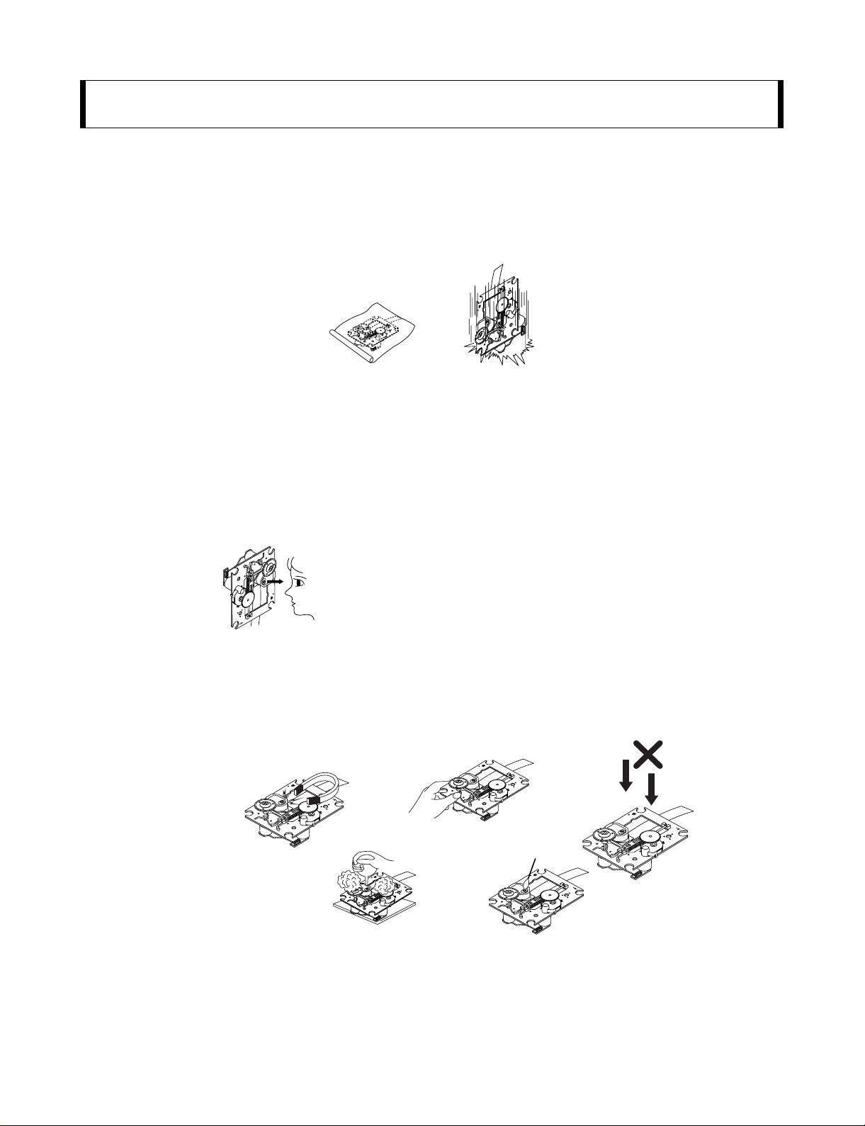
NOTES REGARDING HANDLING OF THE PICK-UP
1. Notes for transport and storage
1) The pick-up should always be left in its conductive bag until immediately prior to use.
2) The pick-up should never be subjected to external pressure or impact.
2. Repair notes
1) The pick-up incorporates a strong magnet, and so should never be brought close to magnetic materials.
2) The pick-up should always be handled correctly and carefully, taking care to avoid external pressure and
impact. If it is subjected to strong pressure or impact, the result may be an operational malfunction and/or
damage to the printed-circuit board.
3) Each and every pick-up is already individually adjusted to a high degree of precision, and for that reason
the adjustment point and installation screws should absolutely never be touched.
4) Laser beams may damage the eyes!
Absolutely never permit laser beams to enter the eyes!
Also NEVER switch ON the power to the laser output part (lens, etc.) of the pick-up if it is damaged.
5) Cleaning the lens surface
If there is dust on the lens surface, the dust should be cleaned away by using an air bush (such as used
for camera lens). The lens is held by a delicate spring. When cleaning the lens surface, therefore, a cotton swab should be used, taking care not to distort this.
6) Never attempt to disassemble the pick-up.
Spring by excess pressure. If the lens is extremely dirty, apply isopropyl alcohol to the cotton swab.
(Do not use any other liquid cleaners, because they will damage the lens.) Take care not to use too much
of this alcohol on the swab, and do not allow the alcohol to get inside the pick-up.
Storage in conductive bag
Drop impact
NEVER look directly at the laser beam, and don’t let
contact fingers or other exposed skin.
Magnet
How to hold the pick-up
Conductive Sheet
Cotton swab
Pressure
Pressure
SECTION 1. GENERAL
1-3
NOTES REGARDING COMPACT DISC PLAYER REPAIRS
1. Preparations
1) Compact disc players incorporate a great many ICs as well as the pick-up (laser diode). These components
are sensitive to, and easily affected by, static electricity. If such static electricity is high voltage, components
can be damaged, and for that reason components should be handled with care.
2) The pick-up is composed of many optical components and other high-precision components. Care must be
taken, therefore, to avoid repair or storage where the temperature of humidity is high, where strong magnetism is present, or where there is excessive dust.
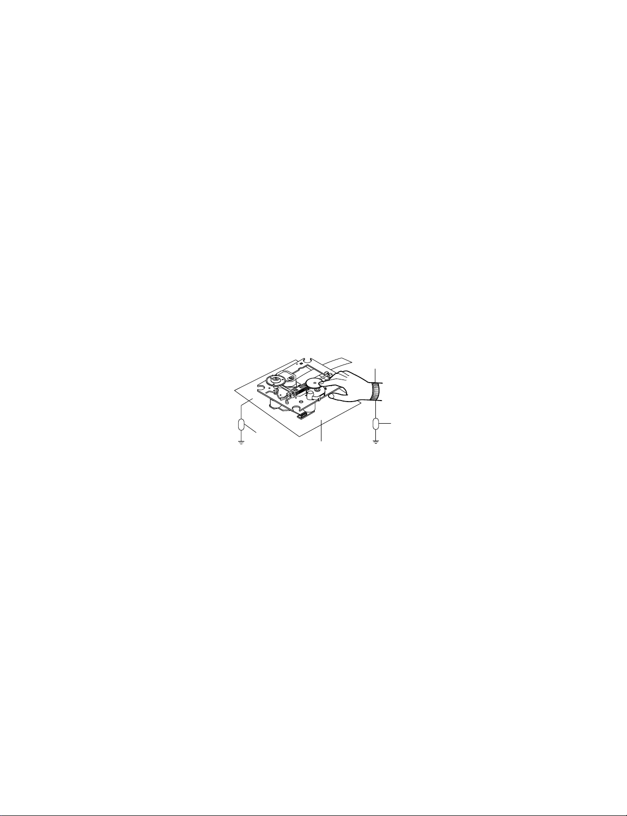
2. Notes for repair
1) Before replacing a component part, first disconnect the power supply lead wire from the unit
2) All equipment, measuring instruments and tools must be grounded.
3) The workbench should be covered with a conductive sheet and grounded.
When removing the laser pick-up from its conductive bag, do not place the pick-up on the bag. (This is
because there is the possibility of damage by static electricity.)
4) To prevent AC leakage, the metal part of the soldering iron should be grounded.
5) Workers should be grounded by an armband (1M Ω)
6) Care should be taken not to permit the laser pick-up to come in contact with clothing, in order to prevent
static electricity changes in the clothing to escape from the armband.
7) The laser beam from the pick-up should NEVER be directly facing the eyes or bare skin.
Resistor
(1 Mohm)
Conductive
Sheet
Resistor
(1 Mohm)
Armband
1-4
ESD PRECAUTIONS
Electrostatically Sensitive Devices (ESD)
Some semiconductor (solid state) devices can be damaged easily by static electricity. Such components
commonly are called Electrostatically Sensitive Devices (ESD). Examples of typical ESD devices are integrated
circuits and some field-effect transistors and semiconductor chip components. The following techniques should
be used to help reduce the incidence of component damage caused by static electricity.
1. Immediately before handling any semiconductor component or semiconductor-equipped assembly, drain off
any electrostatic charge on your body by touching a known earth ground. Alternatively, obtain and wear a
commercially available discharging wrist strap device, which should be removed for potential shock reasons
prior to applying power to the unit under test.
2. After removing an electrical assembly equipped with ESD devices, place the assembly on a conductive surface
such as aluminum foil, to prevent electrostatic charge buildup or exposure of the assembly.
3. Use only a grounded-tip soldering iron to solder or unsolder ESD devices.
4. Use only an anti-static solder removal device. Some solder removal devices not classified as "anti-static" can
generate electrical charges sufficient to damage ESD devices.
5. Do not use freon-propelled chemicals. These can generate electrical charges sufficient to damage ESD
devices.
6. Do not remove a replacement ESD device from its protective package until immediately before you are
ready to install it. (Most replacement ESD devices are packaged with leads electrically shorted together by
conductive foam, aluminum foil or comparable conductive materials).
7. Immediately before removing the protective material from the leads of a replacement ESD device, touch the
protective material to the chassis or circuit assembly into which the device will by installed.
CAUTION : BE SURE NO POWER IS APPLIED TO THE CHASSIS OR CIRCUIT, AND OBSERVE ALL OTHER
SAFETY PRECAUTIONS.
8. Minimize bodily motions when handing unpackaged replacement ESD devices. (Otherwise harmless motion
such as the brushing together of your clothes fabric or the lifting of your foot from a carpeted floor can generate static electricity sufficient to damage an ESD device).
CAUTION. GRAPHIC SYMBOLS
THE LIGHTNING FLASH WITH APROWHEAD SYMBOL. WITHIN AN EQUILATERAL TRIANGLE, IS
INTENDED TO ALERT THE SERVICE PERSONNEL TO THE PRESENCE OF UNINSULATED
“DANGEROUS VOLTAGE” THAT MAY BE OF SUFFICIENT MAGNITUDE TO CONSTITUTE ARISK OF
ELECTRIC SHOCK.
THE EXCLAMATION POINTWITHIN AN EQUILATERAL TRIANGLE IS INTENDED TO ALERT THE
SERVICE PERSONNEL TO THE PRESENCE OF IMPORTANT SAFETY INFORMATION IN SERVICE
LITERATURE.

1-5
GENERAL
Power supply Refer to main label
Power consumption Refer to main label
Weight 3.9 kg
External dimensions (W x H x D) 430 x 54 x 350 mm
Operating conditions Temperature: 5°C to 35°C, Operation status: Horizontal
Operating humidity 5% to 85%
CD/DVD
Laser Semiconductor laser, wavelength 650 nm
Signal system PAL 625/50, NTSC 525/60
Frequency response (audio) 200 Hz to 20 kHz
Signal-to-noise ratio (audio) More than 75 dB (1 kHz, NOP, 20 kHz LPF/A-Filter)
Dynamic range (audio) More than 70 dB
Harmonic distortion (audio) 0.5 % (1 kHz, at 12W position) (20 kHz LPF/A-Filter)
VIDEO
Video input 1.0 V (p-p), 75 Ω, negative sync., RCA jack x 1
Video output 1.0 V (p-p), 75 Ω, negative sync., RCA jack x 1
S-video output (Y) 1.0 V (p-p), 75 Ω, negative sync., Mini DIN 4-pin x 1
(C) 0.3 V (p-p), 75 Ω
Component Video output (Y) 1.0 V (p-p), 75 Ω, negative sync., RCA jack x 1
(Pb)/(Pr) 0.7 V (p-p), 75 Ω, RCA jack x 1
TUNER
FM
Tuning Range 87.5 - 108.0 MHz or 65.0 - 74.0 MHz, 87.5 - 108.0 MHz
Intermediate Frequency 10.7 MHz
Signal-to Noise Ratio 60 dB (Mono)
Frequency Response 140 - 10,000 Hz
AM [MW]
Tuning Range 522 - 1,620 kHz or 520 - 1,720 kHz
Intermediate Frequency 450 kHz
AMPLIFIER
Stereo mode 70W + 70W (8Ω at 1 kHz, THD 10 %)
Surround mode Front: 70W + 70W (THD 10 %)
Center*: 70W
Surround*: 70W + 70W (8Ω at 1 kHz, THD 10 %)
Subwoofer*: 150W (4Ω at 30 Hz, THD 10 %)
Input AV IN
Outputs S-VIDEO, MONITOR, PHONES: (32 Ω, 10.V)
WIRELESS TX (ACC25T) Transmission Output : 2.4GHz, Power Supply : DC 7V
WIRELESS RX (ACC25R) Reception Output : 2.4GHz, Amplifier : 70W + 70W (8Ω, THD 0.1 %)
SPEAKERS
Front Speaker Center Speaker Subwoofer Wireless Speaker
Type 1 Way 2 Speaker 1 Way 2 Speaker 1 Way 1 Speaker 1 Way 2 Speaker
Impedance 8 Ω 8 Ω 4 Ω 8 Ω
Frequency Response
150 - 20000 Hz 150 - 20000 Hz 40 - 1500 Hz 150 - 20000 Hz
Sound Pressure Level
86 dB/W (1m) 86 dB/W (1m) 82 dB/W (1m) 86 dB/W (1m)
Rated Input Power 70W 70W 150W 70W
Max. Input Power 140W 140W 300W 140W
Net Dimensions 280x1200x280 mm 500x83x90 mm 195x402x360 mm 280x1200x280 mm
Net Weight 2.38 kg 0.71 kg 6.2 kg 2.38 kg
(* Depending on the sound mode
settings and the source, there
may be no sound output.)
SPECIFICATIONS

2-1
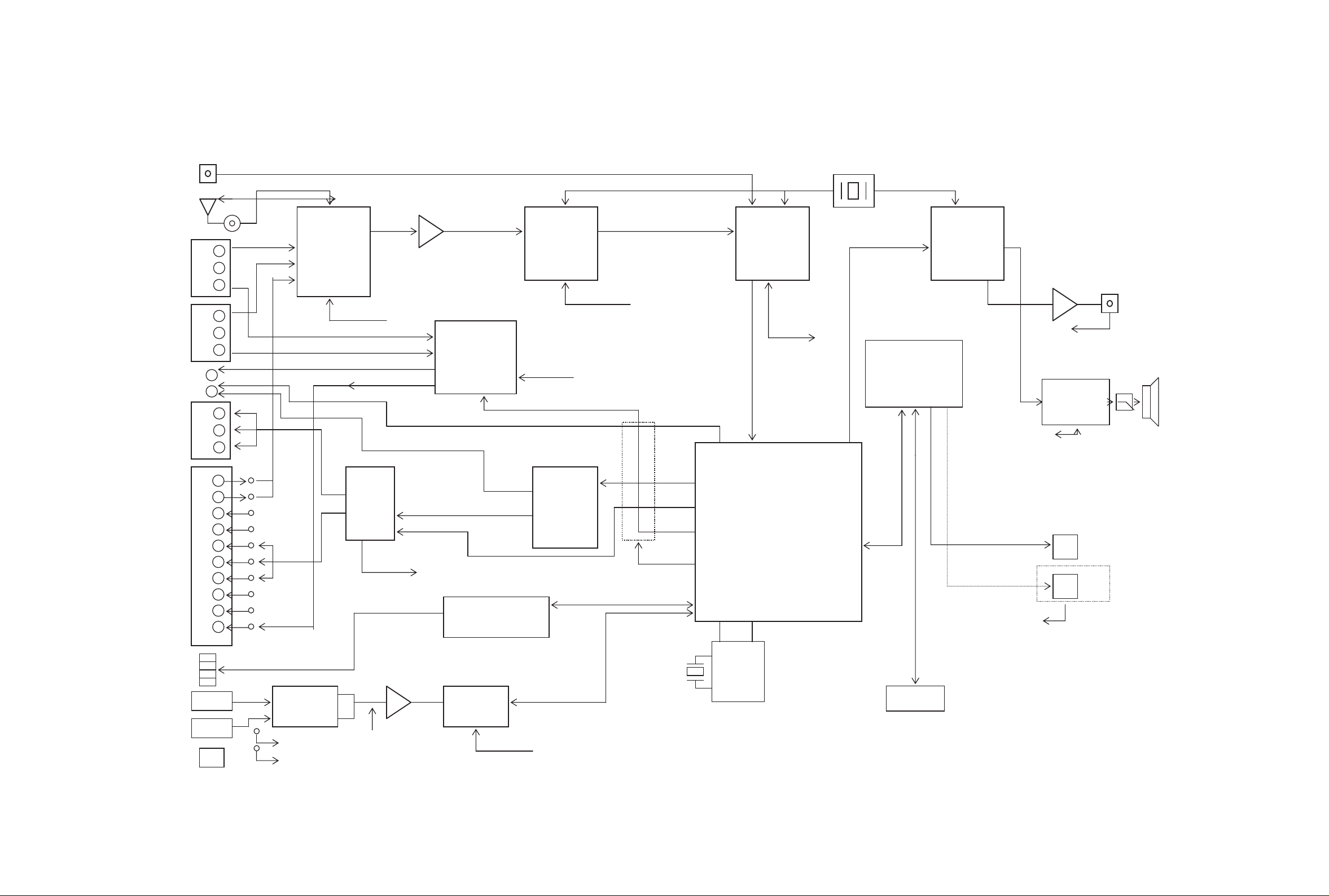
SECTION 2. AUDIO PART
AUDIO TROUBLESHOOTING GUIDE
1. POWER SUPPLY CIRCUIT

2-2
2. FRONT CIRCUIT (1/2)
PIN3
PIN4
PIN9
CN902 CN902
: -32.4 VKK
: -27.5 FL: -23.7 FL+
: +5.0

2-3
3. FRONT CIRCUIT (2/2)
2-4 2-5
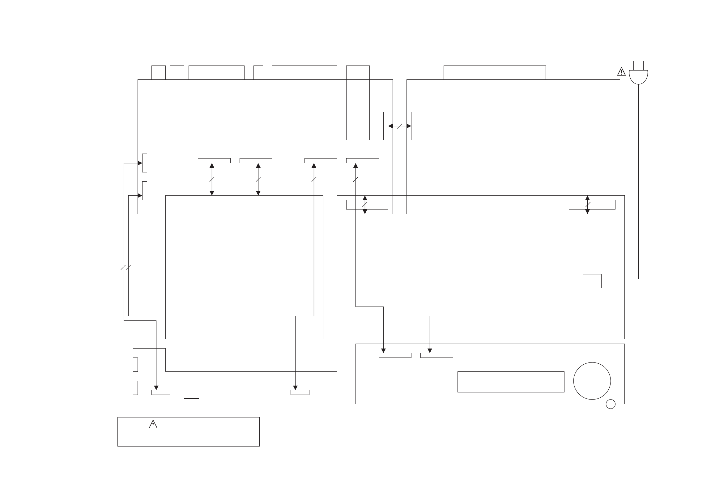
WIRING DIAGRAM
WIRELESS
PN801
CN350
OPTICALINSCART
JACK
MAIN PCB
PDM01 PDM03
23PIN 11PIN 24PIN 23PIN
OPTION
SW
AV1,2
COMPONENT
MONITOR OUT
S-VIDEO OUT
PN103
TUNER
PN104
SPEAKER TERMINAL
30PIN
PN302
AMP PCB
PN105
PN902 PN303
14PIN 14PIN
5PIN
6PIN
MIC
JACK
MIC
JACK
CN001
NOTES) Warning
NOTES) Parts that are shaded are critical
NOTES) With respect to risk of fire or
NOTES) electricial shock.
MIC&USB PCB
USB JACK
MD
PN005
PN002
PN001
SMPS PCB
VFD
FRONT
FRONT
PCB
PCB
H/P JACK
2-6 2-7
BLOCK DIAGRAM
Optical
Tuner
AV1
AV2
(option)
Monitor Out
S-AV
Component
Scart
(option)
USB Port
MIC
Wireless
L
R
V
L
R
V
G
B
R
L
R
L
R
G
B
R
8
16
V
MIC1
MIC2
7V
Tuner-L/R
AV1-L/R
AV2-L/R
SCART-L/R
SCART-ID
SCART-FB
(A)(T_CE,T_DO,T_DI,T_CLK,T_RDS_DATA,T_RDS,CLK)
Audio s/w
Bu 4052
CTL-A/B
AV1-CVBS
AV2-CVBS
Monitor out
SCART-CVBS out
C
Y
ALC
BA 3308
MIC1_DET(A)
MIC2_DET(A)
(B)
Slide
S/W
VIDEO-SW
Mixing
+
P
(R) ,Pr(R)
b
(A)
Video S/W
NJM 2279
out
(CVBS-S/W)
DVD-CVBS
Y
Y(G)
USB Controller
CS 5340
ADC
/RST-AD
ADC
CS 5340
Fs = 48kHz
Fx
/RST-AD
SW1, SW2,MUTE1
(A)
Video
S/W
NJM2279
(Y-S/W)
ALRCK,ABCK
MCLK,AMDAT
(A)
SPDI
F
AD-DATA
AD-BCK
AD-LRCK
(A)
C
YY
DVD BLOCK
CVBS
MUTE
TR Mute
Mic Volume : OSD CTL
SS
T
DIT
CS 8406
(slave)
8406_SDI,8406_SDO
8406_CLK,8406_CE
8406_RST,8406_INT
(A)
SPDIF
(ES 6698)
OPTION
12.288MHz
LRCK
BCK
ADAT 0,1,2,3
(FL/R,RL/R,C/SW)
AUDIO MICOM
LC876B48
(PIN MAP )
FRONT
PS 9818
(PWM)
(A) HP_DET
STA510A
AMP IC
AM
(A)
FAN1_CTL
FAN2_CTL
PDN
TH_W
FAN1
FAN2
H/P
OPTION
2-8 2-9
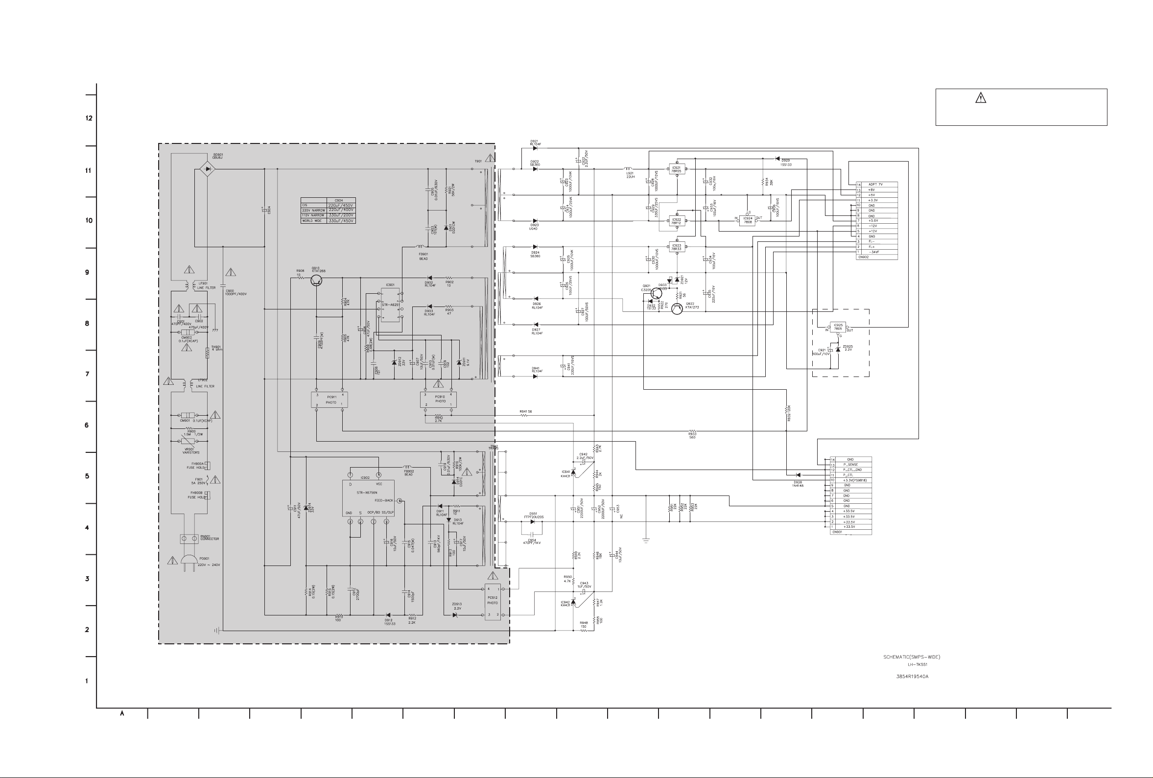
SCHEMATIC DIAGRAMS
1. POWER SCHEMATIC DIAGRAM_1
A B C D E F G H I J K L M N O P Q R ST
NOTES) Warning
NOTES) Parts that are shaded are critical
NOTES) With respect to risk of fire or
NOTES) electricial shock.
2-10 2-11
2. POWER SCHEMATIC DIAGRAM_2
A B C D E F G H I J K L M N O P Q R ST
2-12 2-13
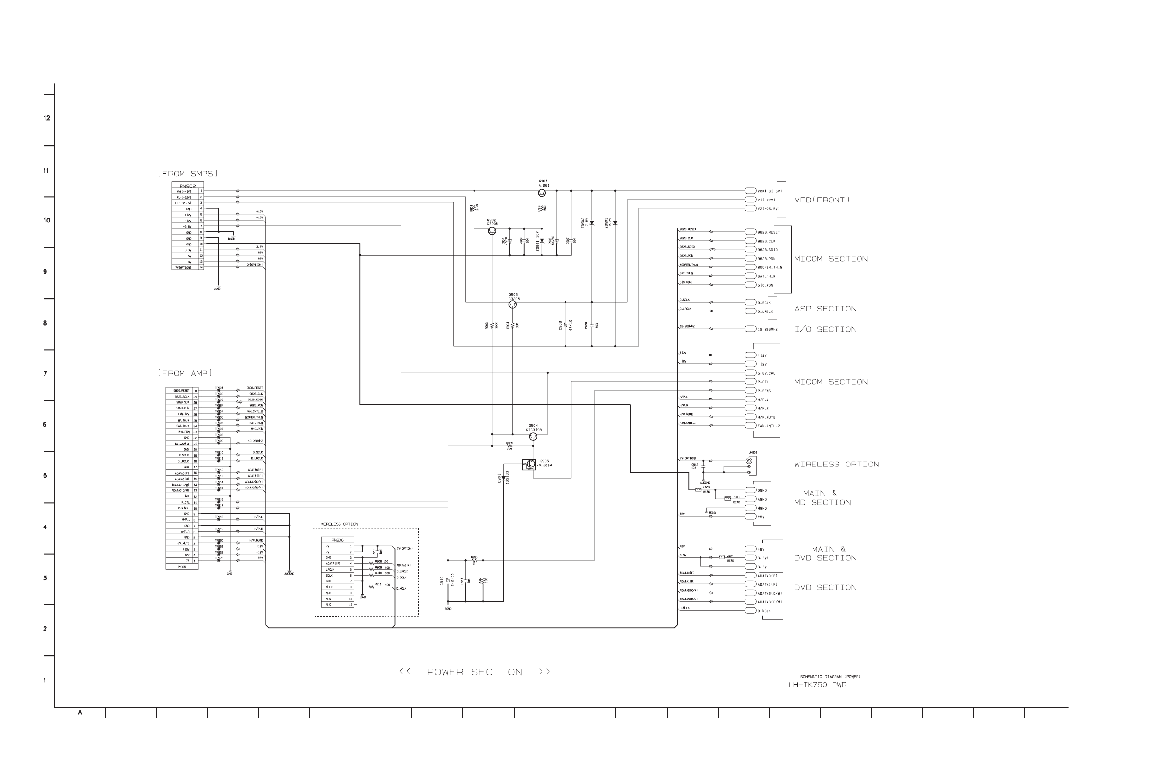
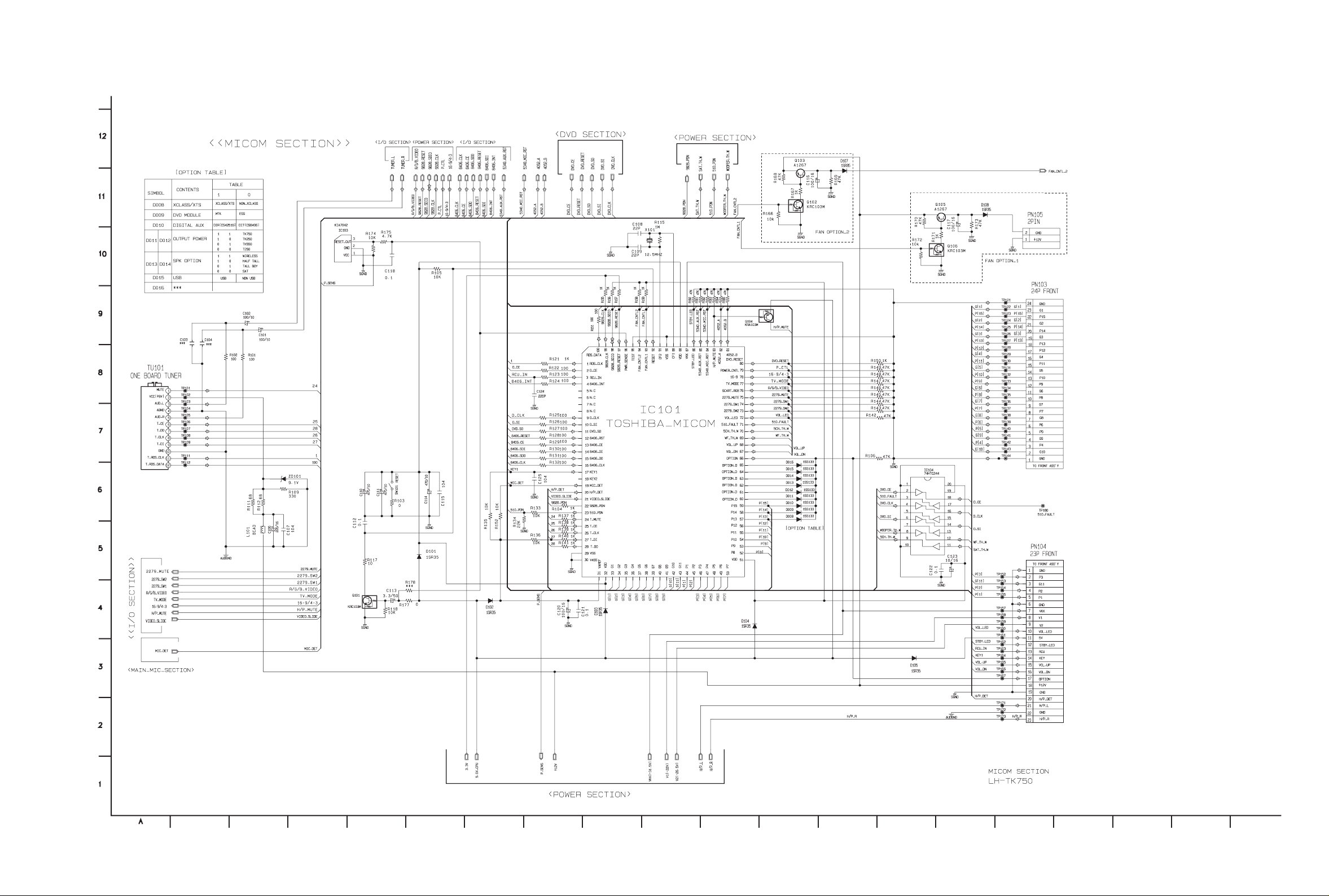
3. MICOM SCHEMATIC DIAGRAM
A B C D E F G H I J K L M N O P Q R ST
2-14 2-15
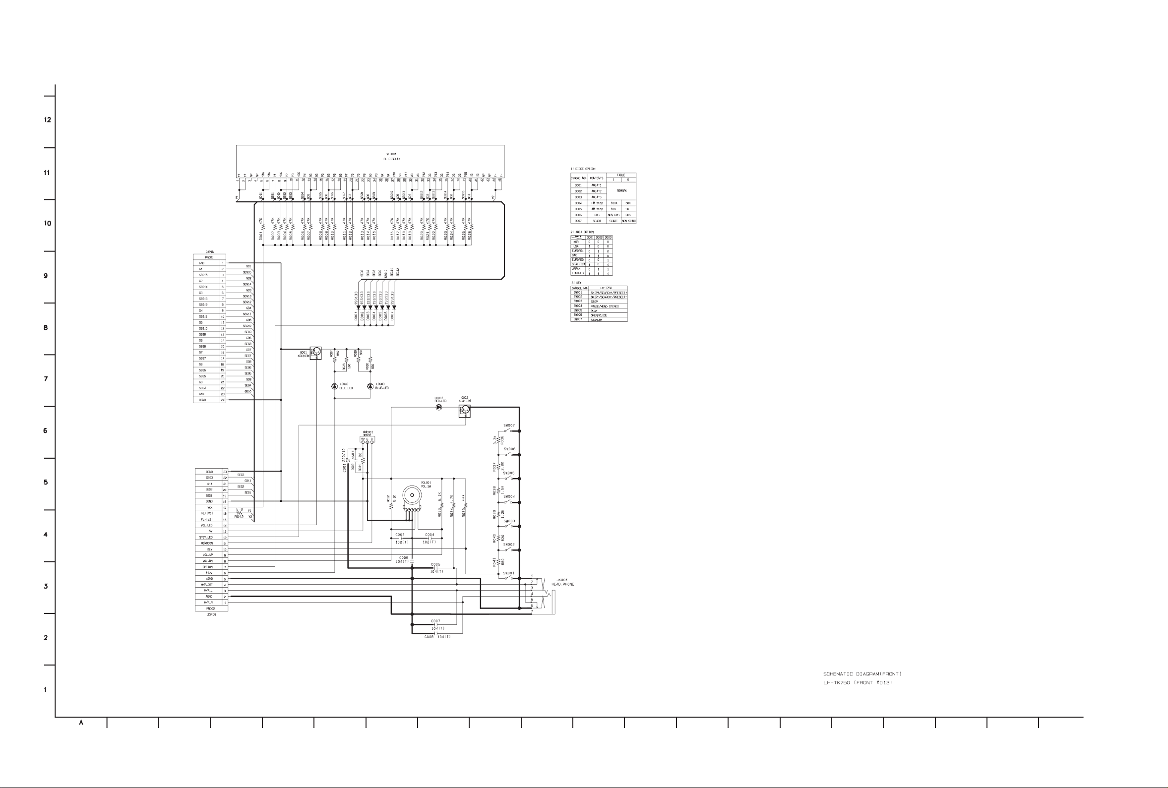
4. FRONT SCHEMATIC DIAGRAM
A B C D E F G H I J K L M N O P Q R ST

2-16 2-17
5. DSP& SCHEMATIC DIAGRAM
A B C D E F G H I J K L M N O P Q R ST

2-18 2-19
6. I/O SCHEMATIC DIAGRAM
A B C D E F G H I J K L M N O P Q R ST
2-20 2-21
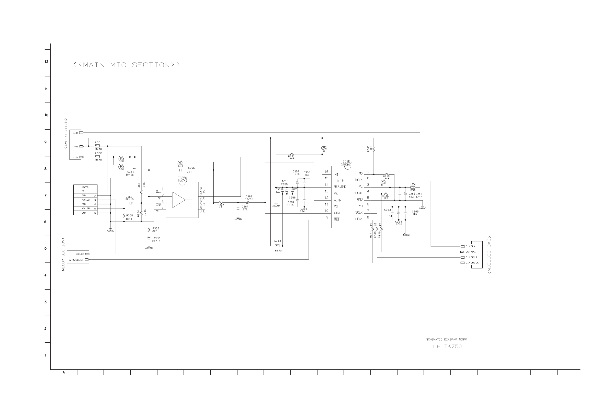
7. MAIN MIC SCHEMATIC DIAGRAM
A B C D E F G H I J K L M N O P Q R ST

2-22 2-23
PRINTED CIRCUIT BOARD DIAGRAMS
1. MAIN/DVD P.C. BOARD DIAGRAM ( TOP VIEW )
2-24 2-25
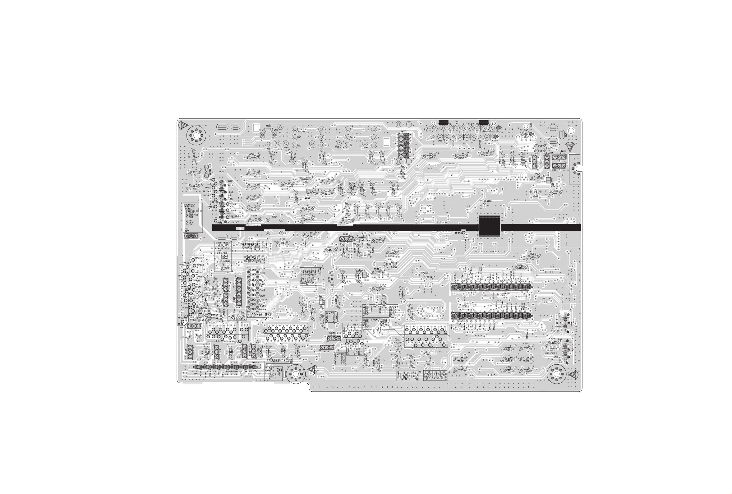
2. MAIN/DVD P.C. BOARD DIAGRAM ( BOTTOM VIEW )
6870R7505AC

2-26 2-27
3. FRONT MIC P.C. BOARD
6870R7507AA

2-28 2-29
4. SMPS P.C. BOARD
LOCATION GUIDE
NOTES) Warning
NOTES) Parts that are shaded are critical
NOTES) With respect to risk of fire or
NOTES) electricial shock.
5. MIC P.C. BOARD
( 5 TOOL )
LOCATION GUIDE
NOTES) Warning
NOTES) Parts that are shaded are critical
NOTES) With respect to risk of fire or
NOTES) electricial shock.
( 7 TOOL )
( TOP VIEW )
( BOTTOM VIEW )
2-30 2-31
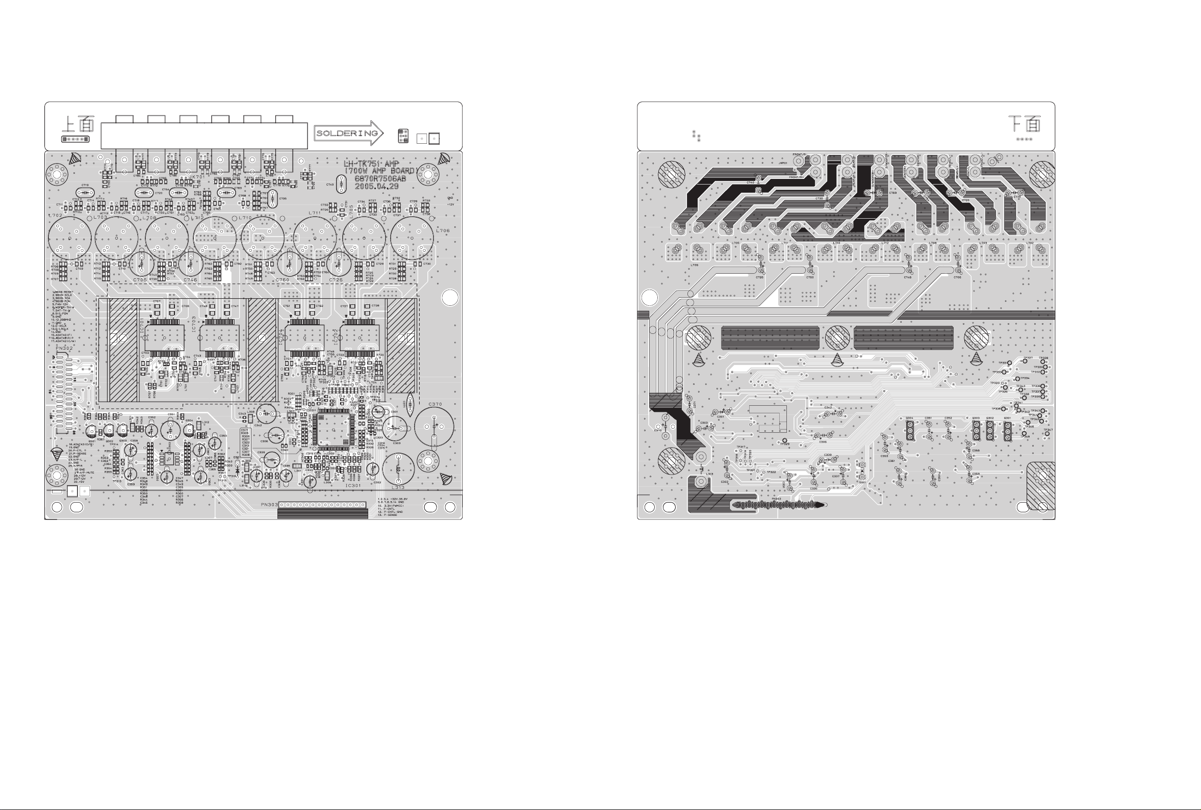
6. AMP P.C. BOARD
( TOP VIEW ) ( BOTTOM VIEW )
3-1
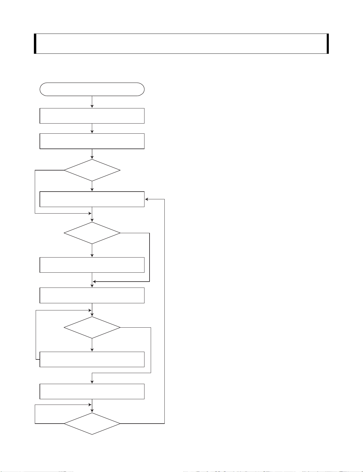
ELECTRICAL TROUBLESHOOTING GUIDE
1. System operation flow
SECTION 3. DVD & AMP PART
Power On
1. 8082 initializes SERVO, DSP & RISC registers
2. Write RISC code to SDRAM
3. Reset RISC
Show LOGO
Yes
SLED Moves to Inner Position
1. Judge whether have disc and disc type
2. Jump to related disc reading procedure
Tray Closed?
No
Tray Close to Closed position
SLED at Inner
Side?
No
Recieve
OPEN/ CLOSE
Key?
Yes
No
1. Execute Pressed Key & IR Key
2. Systemoperati on Routi ne Loop
1. Stop Playback & Open Tray
2. Display tray open message & LOGO
No
Receive
CLOSE Key?
Yes

3-2
2. Test & debug flow
TEST
Check the
AC Vol tage
Power PCBA (110V
or 220V)
Yes
Switch on the Power PCBA
Is the
DC Voltage
outputs OK? (-44V, -22V,
-26.5V, ±12V, 5.6V, 3.3V,
5V, 7V, 8V)
Yes
Are 3.3V and 5V DC
outputs normal on main
PCBA?
Yes
Update
FLASH
successfully?
No
No
No
No
Check the POWER PART
Check the POWER PART
Check the regulators or diode.
1. Check 27MHz system clock.
2. Check systemreset circuit.
3. Check FLASH R/Wenable signal PRD,
RWR.
4. Check FLASH Memory related circuit.
Yes
Replace FLASH
A
 Loading...