

Page 1

WIRELESS DVD RECEIVER
SERVICE MANUAL
MODEL : LH-W551TB
LHS-55TBC, LHS-55TBS,
LHS-55TBW,
ACC55T, ACC55R
MODEL : LH-W551TB LHS-55TBC, LHS-55TBS, LHS-55TBW, ACC55T, ACC55R
SERVICE MANUAL
Page 2

1-1
[CONTENTS]
SECTION 1. GENERAL
• SERVICING PRECAUTIONS . . . . . . . . . . . . . . . . . . . . . . . . . . . . . . . . . . . . . . . . . . . . . . . 1-2
• ESD PRECAUTIONS . . . . . . . . . . . . . . . . . . . . . . . . . . . . . . . . . . . . . . . . . . . . . . . . . . . . 1-4
• SPECIFICATIONS . . . . . . . . . . . . . . . . . . . . . . . . . . . . . . . . . . . . . . . . . . . . . . . . . . . . . . . .1-5
SECTION 2. AUDIO PART
• AUDIO TROUBLESHOOTING GUIDE . . . . . . . . . . . . . . . . . . . . . . . . . . . . . . . . . . . . . . . . 2-1
• WIRING DIAGRAM . . . . . . . . . . . . . . . . . . . . . . . . . . . . . . . . . . . . . . . . . . . . . . . . . . . . . . . 2-4
• BLOCK DIAGRAM . . . . . . . . . . . . . . . . . . . . . . . . . . . . . . . . . . . . . . . . . . . . . . . . . . . . . . . 2-6
• SCHEMATIC DIAGRAMS . . . . . . . . . . . . . . . . . . . . . . . . . . . . . . . . . . . . . . . . . . . . . . . . . 2-8
• PRINTED CIRCUIT DIARGAMS . . . . . . . . . . . . . . . . . . . . . . . . . . . . . . . . . . . . . . . . . . . . 2-22
SECTION 3. DVD & AMP PART
• ELECTRICAL TROUBLESHOOTING GUIDE . . . . . . . . . . . . . . . . . . . . . . . . . . . . . . . . . . .3-1
• DVD PART SCHEMATIC DIAGRAMS . . . . . . . . . . . . . . . . . . . . . . . . . . . . . . . . . . . . . . . .3-22
SECTION 4. EXPLODED VIEWS . . . . . . . . . . . . . . . . . . . . . . . . . . . . . . . . . . . . .4-1
SECTION 5. SPEAKER PART . . . . . . . . . . . . . . . . . . . . . . . . . . . . . . . . . . . . . . .5-1
SECTION 6. REPLACEMENT PARTS LIST . . . . . . . . . . . . . . . . . . . . . . . . . . . . .6-1
Page 3
1-2
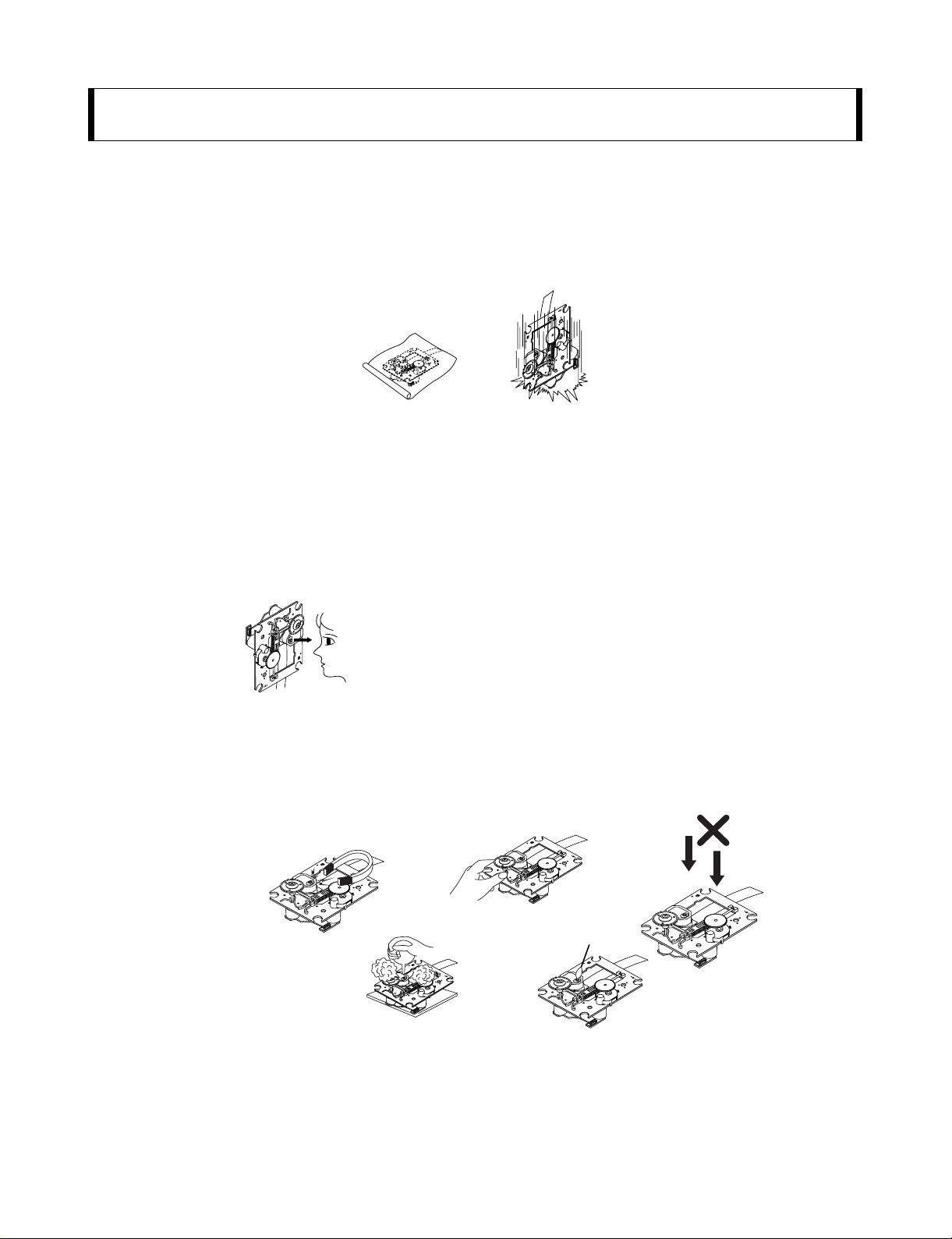
SERVICING PRECAUTIONS
NOTES REGARDING HANDLING OF THE PICK-UP
1. Notes for transport and storage
1) The pick-up should always be left in its conductive bag until immediately prior to use.
2) The pick-up should never be subjected to external pressure or impact.
2. Repair notes
1) The pick-up incorporates a strong magnet, and so should never be brought close to magnetic materials.
2) The pick-up should always be handled correctly and carefully, taking care to avoid external pressure and
impact. If it is subjected to strong pressure or impact, the result may be an operational malfunction and/or
damage to the printed-circuit board.
3) Each and every pick-up is already individually adjusted to a high degree of precision, and for that reason
the adjustment point and installation screws should absolutely never be touched.
4) Laser beams may damage the eyes!
Absolutely never permit laser beams to enter the eyes!
Also NEVER switch ON the power to the laser output part (lens, etc.) of the pick-up if it is damaged.
5) Cleaning the lens surface
If there is dust on the lens surface, the dust should be cleaned away by using an air bush (such as used
for camera lens). The lens is held by a delicate spring. When cleaning the lens surface, therefore, a cotton swab should be used, taking care not to distort this.
6) Never attempt to disassemble the pick-up.
Spring by excess pressure. If the lens is extremely dirty, apply isopropyl alcohol to the cotton swab.
(Do not use any other liquid cleaners, because they will damage the lens.) Take care not to use too much
of this alcohol on the swab, and do not allow the alcohol to get inside the pick-up.
Storage in conductive bag
Drop impact
NEVER look directly at the laser beam, and don’t let
contact fingers or other exposed skin.
Magnet
How to hold the pick-up
Conductive Sheet
Cotton swab
Pressure
Pressure
SECTION 1. GENERAL
Page 4
1-3
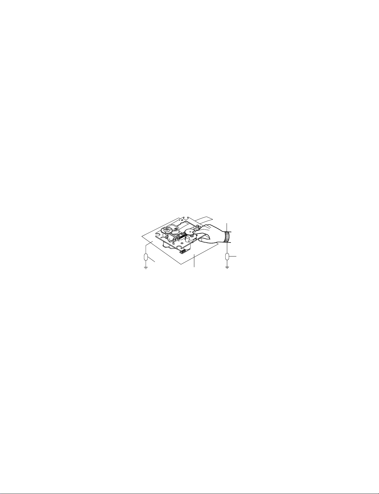
NOTES REGARDING COMPACT DISC PLAYER REPAIRS
1. Preparations
1) Compact disc players incorporate a great many ICs as well as the pick-up (laser diode). These components
are sensitive to, and easily affected by, static electricity. If such static electricity is high voltage, components
can be damaged, and for that reason components should be handled with care.
2) The pick-up is composed of many optical components and other high-precision components. Care must be
taken, therefore, to avoid repair or storage where the temperature of humidity is high, where strong magnetism is present, or where there is excessive dust.
2. Notes for repair
1) Before replacing a component part, first disconnect the power supply lead wire from the unit
2) All equipment, measuring instruments and tools must be grounded.
3) The workbench should be covered with a conductive sheet and grounded.
When removing the laser pick-up from its conductive bag, do not place the pick-up on the bag. (This is
because there is the possibility of damage by static electricity.)
4) To prevent AC leakage, the metal part of the soldering iron should be grounded.
5) Workers should be grounded by an armband (1M Ω)
6) Care should be taken not to permit the laser pick-up to come in contact with clothing, in order to prevent
static electricity changes in the clothing to escape from the armband.
7) The laser beam from the pick-up should NEVER be directly facing the eyes or bare skin.
Resistor
(1 Mohm)
Conductive
Sheet
Resistor
(1 Mohm)
Armband
Page 5
1-4
ESD PRECAUTIONS
Electrostatically Sensitive Devices (ESD)
Some semiconductor (solid state) devices can be damaged easily by static electricity. Such components
commonly are called Electrostatically Sensitive Devices (ESD). Examples of typical ESD devices are integrated
circuits and some field-effect transistors and semiconductor chip components. The following techniques should
be used to help reduce the incidence of component damage caused by static electricity.
1. Immediately before handling any semiconductor component or semiconductor-equipped assembly, drain off
any electrostatic charge on your body by touching a known earth ground. Alternatively, obtain and wear a
commercially available discharging wrist strap device, which should be removed for potential shock reasons
prior to applying power to the unit under test.
2. After removing an electrical assembly equipped with ESD devices, place the assembly on a conductive surface
such as aluminum foil, to prevent electrostatic charge buildup or exposure of the assembly.
3. Use only a grounded-tip soldering iron to solder or unsolder ESD devices.
4. Use only an anti-static solder removal device. Some solder removal devices not classified as "anti-static" can
generate electrical charges sufficient to damage ESD devices.
5. Do not use freon-propelled chemicals. These can generate electrical charges sufficient to damage ESD
devices.
6. Do not remove a replacement ESD device from its protective package until immediately before you are
ready to install it. (Most replacement ESD devices are packaged with leads electrically shorted together by
conductive foam, aluminum foil or comparable conductive materials).
7. Immediately before removing the protective material from the leads of a replacement ESD device, touch the
protective material to the chassis or circuit assembly into which the device will by installed.
CAUTION : BE SURE NO POWER IS APPLIED TO THE CHASSIS OR CIRCUIT, AND OBSERVE ALL OTHER
SAFETY PRECAUTIONS.
8. Minimize bodily motions when handing unpackaged replacement ESD devices. (Otherwise harmless motion
such as the brushing together of your clothes fabric or the lifting of your foot from a carpeted floor can generate static electricity sufficient to damage an ESD device).
CAUTION. GRAPHIC SYMBOLS
THE LIGHTNING FLASH WITH APROWHEAD SYMBOL. WITHIN AN EQUILATERAL TRIANGLE, IS
INTENDED TO ALERT THE SERVICE PERSONNEL TO THE PRESENCE OF UNINSULATED
“DANGEROUS VOLTAGE” THAT MAY BE OF SUFFICIENT MAGNITUDE TO CONSTITUTE ARISK OF
ELECTRIC SHOCK.
THE EXCLAMATION POINTWITHIN AN EQUILATERAL TRIANGLE IS INTENDED TO ALERT THE
SERVICE PERSONNEL TO THE PRESENCE OF IMPORTANT SAFETY INFORMATION IN SERVICE
LITERATURE.
Page 6

1-5
GENERAL
Power supply Refer to main label
Power consumption Refer to main label
Weight 3.9 kg
External dimensions (W x H x D) 430 x 54 x 350 mm
Operating conditions Temperature: 5°C to 35°C, Operation status: Horizontal
Operating humidity 5% to 85%
CD/DVD
Laser Semiconductor laser, wavelength 650 nm
Signal system PAL 625/50, NTSC 525/60
Frequency response (audio) 200 Hz to 20 kHz
Signal-to-noise ratio (audio) More than 75 dB (1 kHz, NOP, 20 kHz LPF/A-Filter)
Dynamic range (audio) More than 70 dB
Harmonic distortion (audio) 0.5 % (1 kHz, at 12W position) (20 kHz LPF/A-Filter)
VIDEO
Video input 1.0 V (p-p), 75 Ω, negative sync., RCA jack x 1
Video output 1.0 V (p-p), 75 Ω, negative sync., RCA jack x 1
S-video output (Y) 1.0 V (p-p), 75 Ω, negative sync., Mini DIN 4-pin x 1
(C) 0.3 V (p-p), 75 Ω
Component Video output (Y) 1.0 V (p-p), 75 Ω, negative sync., RCA jack x 1
(Pb)/(Pr) 0.7 V (p-p), 75 Ω, RCA jack x 1
TUNER
FM
Tuning Range 87.5 - 108.0 MHz or 65.0 - 74.0 MHz, 87.5 - 108.0 MHz
Intermediate Frequency 10.7 MHz
Signal-to Noise Ratio 60 dB (Mono)
Frequency Response 140 - 10,000 Hz
AM [MW]
Tuning Range 522 - 1,620 kHz or 520 - 1,720 kHz
Intermediate Frequency 450 kHz
AMPLIFIER
Stereo mode 70W + 70W (8Ω at 1 kHz, THD 10 %)
Surround mode Front: 70W + 70W (THD 10 %)
Center*: 70W
Surround*: 70W + 70W (8Ω at 1 kHz, THD 10 %)
Subwoofer*: 150W (4Ω at 30 Hz, THD 10 %)
Input AV IN
Outputs S-VIDEO, MONITOR, PHONES: (32 Ω, 10.V)
WIRELESS TX (ACC25T) Transmission Output : 2.4GHz, Power Supply : DC 7V
WIRELESS RX (ACC25R) Reception Output : 2.4GHz, Amplifier : 70W + 70W (8Ω, THD 0.1 %)
SPEAKERS
Front Speaker Center Speaker Subwoofer Wireless Speaker
Type 1 Way 2 Speaker 1 Way 2 Speaker 1 Way 1 Speaker 1 Way 2 Speaker
Impedance 8 Ω 8 Ω 4 Ω 8 Ω
Frequency Response
150 - 20000 Hz 150 - 20000 Hz 40 - 1500 Hz 150 - 20000 Hz
Sound Pressure Level
86 dB/W (1m) 86 dB/W (1m) 82 dB/W (1m) 86 dB/W (1m)
Rated Input Power 70W 70W 150W 70W
Max. Input Power 140W 140W 300W 140W
Net Dimensions 280x1200x280 mm 500x83x90 mm 195x402x360 mm 280x1200x280 mm
Net Weight 2.38 kg 0.71 kg 6.2 kg 2.38 kg
(* Depending on the sound mode
settings and the source, there
may be no sound output.)
SPECIFICATIONS
Page 7

2-1
SECTION 2. AUDIO PART
AUDIO TROUBLESHOOTING GUIDE
1. POWER SUPPLY CIRCUIT
Page 8

2-2
2. FRONT CIRCUIT (1/2)
PIN3
PIN4
PIN9
CN902 CN902
: -32.4 VKK
: -27.5 FL: -23.7 FL+
: +5.0
Page 9

2-3
3. FRONT CIRCUIT (2/2)
Page 10
2-4 2-5
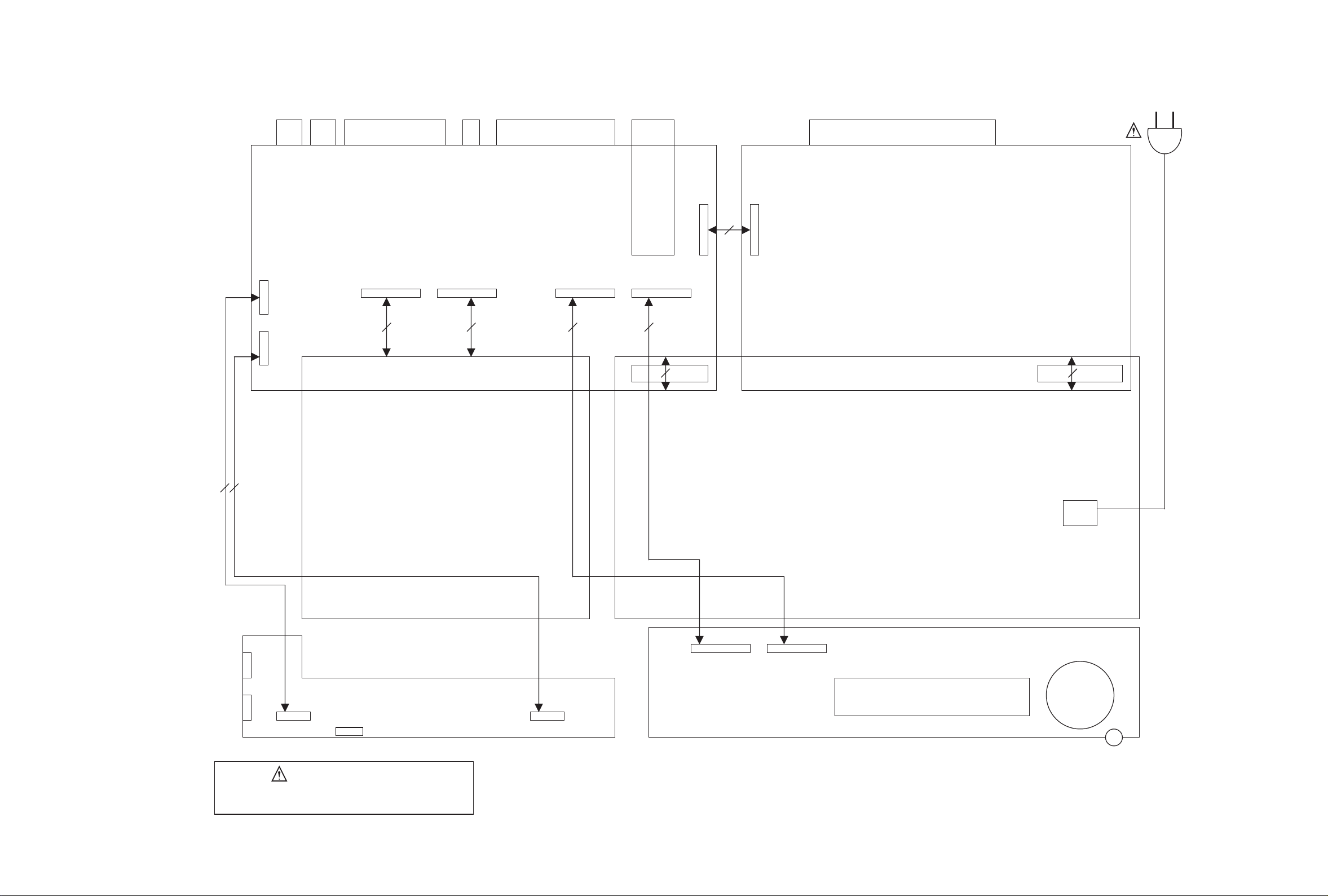
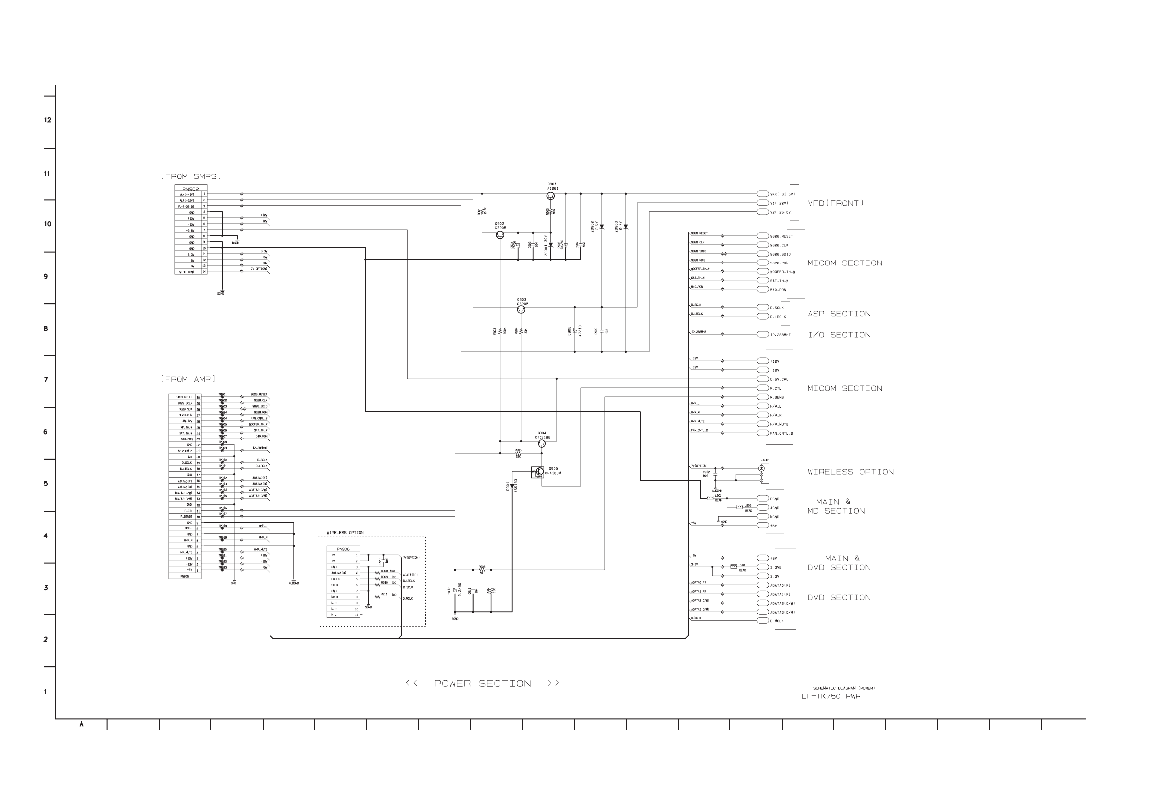
WIRING DIAGRAM
WIRELESS
PN801
CN350
OPTICALINSCART
JACK
MAIN PCB
PDM01 PDM03
23PIN 11PIN 24PIN 23PIN
OPTION
SW
AV1,2
COMPONENT
MONITOR OUT
S-VIDEO OUT
PN103
TUNER
PN104
SPEAKER TERMINAL
30PIN
PN302
AMP PCB
PN105
PN902 PN303
14PIN 14PIN
5PIN
6PIN
MIC
JACK
MIC
JACK
CN001
NOTES) Warning
NOTES) Parts that are shaded are critical
NOTES) With respect to risk of fire or
NOTES) electricial shock.
MIC&USB PCB
USB JACK
MD
PN005
PN002
PN001
SMPS PCB
VFD
FRONT
FRONT
PCB
PCB
H/P JACK
Page 11
2-6 2-7
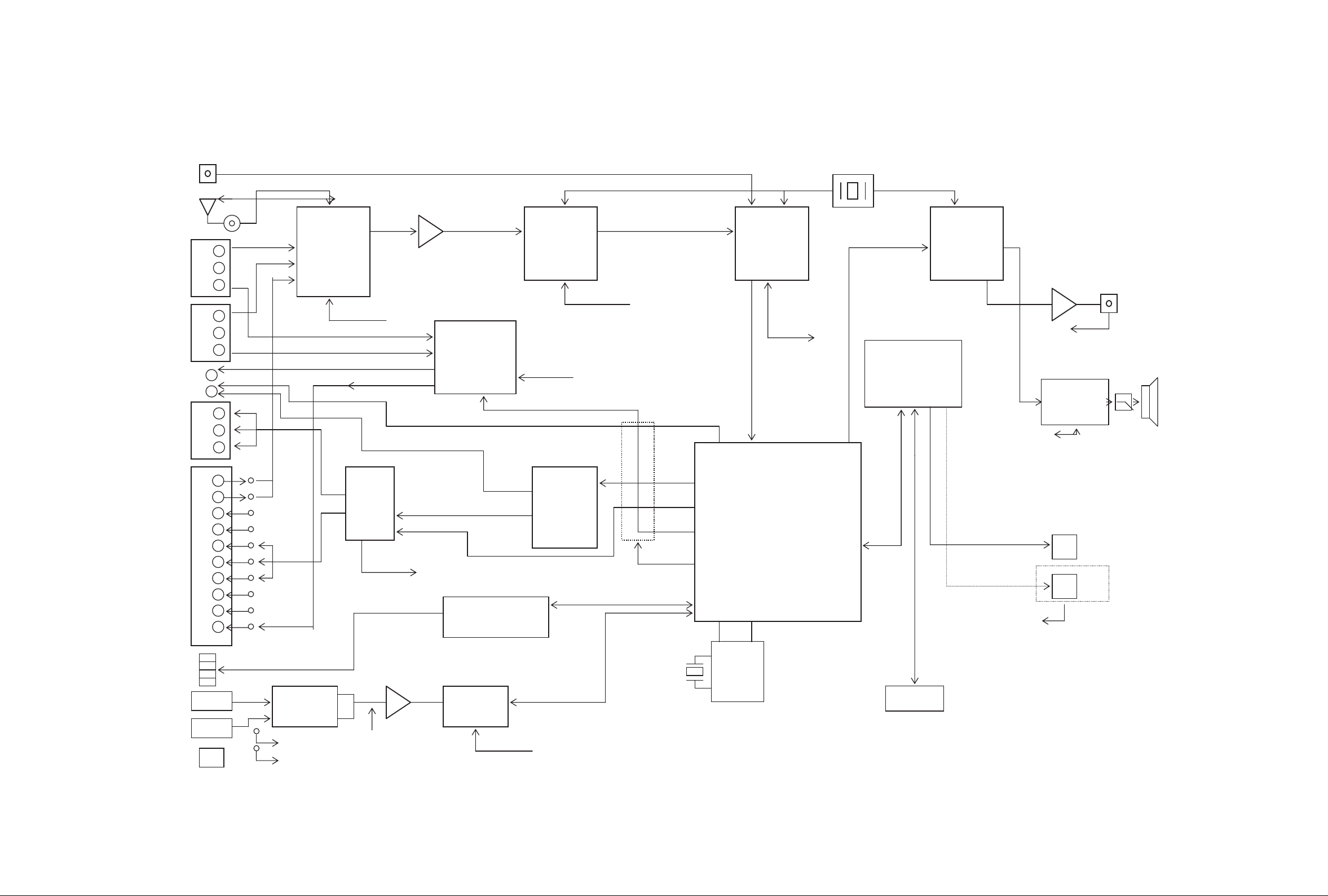
BLOCK DIAGRAM
Optical
Tuner
AV1
AV2
(option)
Monitor Out
S-AV
Component
Scart
(option)
USB Port
MIC
Wireless
L
R
V
L
R
V
G
B
R
L
R
L
R
G
B
R
8
16
V
MIC1
MIC2
7V
Tuner-L/R
AV1-L/R
AV2-L/R
SCART-L/R
SCART-ID
SCART-FB
(A)(T_CE,T_DO,T_DI,T_CLK,T_RDS_DATA,T_RDS,CLK)
Audio s/w
Bu 4052
CTL-A/B
AV1-CVBS
AV2-CVBS
Monitor out
SCART-CVBS out
C
Y
ALC
BA 3308
MIC1_DET(A)
MIC2_DET(A)
(B)
Slide
S/W
VIDEO-SW
Mixing
+
P
(R) ,Pr(R)
b
(A)
Video S/W
NJM 2279
out
(CVBS-S/W)
DVD-CVBS
Y
Y(G)
USB Controller
CS 5340
ADC
/RST-AD
ADC
CS 5340
Fs = 48kHz
Fx
/RST-AD
SW1, SW2,MUTE1
(A)
Video
S/W
NJM2279
(Y-S/W)
ALRCK,ABCK
MCLK,AMDAT
(A)
SPDI
F
AD-DATA
AD-BCK
AD-LRCK
(A)
C
YY
DVD BLOCK
CVBS
MUTE
TR Mute
Mic Volume : OSD CTL
SS
T
DIT
CS 8406
(slave)
8406_SDI,8406_SDO
8406_CLK,8406_CE
8406_RST,8406_INT
(A)
SPDIF
(ES 6698)
OPTION
12.288MHz
LRCK
BCK
ADAT 0,1,2,3
(FL/R,RL/R,C/SW)
AUDIO MICOM
LC876B48
(PIN MAP )
FRONT
PS 9818
(PWM)
(A) HP_DET
STA510A
AMP IC
AM
(A)
FAN1_CTL
FAN2_CTL
PDN
TH_W
FAN1
FAN2
H/P
OPTION
Page 12
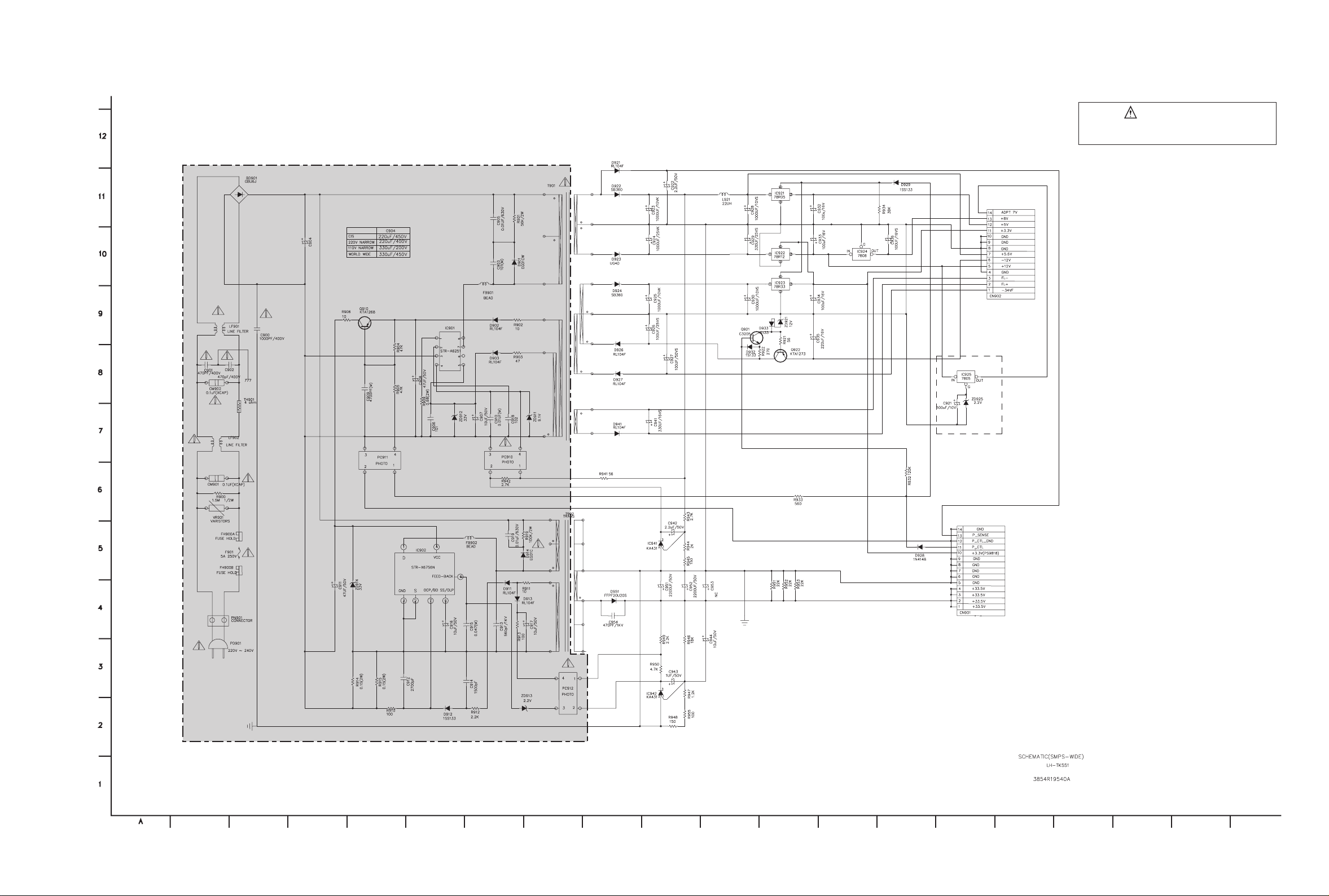
2-8 2-9
SCHEMATIC DIAGRAMS
1. POWER SCHEMATIC DIAGRAM_1
A B C D E F G H I J K L M N O P Q R ST
NOTES) Warning
NOTES) Parts that are shaded are critical
NOTES) With respect to risk of fire or
NOTES) electricial shock.
Page 13
2-10 2-11
2. POWER SCHEMATIC DIAGRAM_2
A B C D E F G H I J K L M N O P Q R ST
Page 14
2-12 2-13
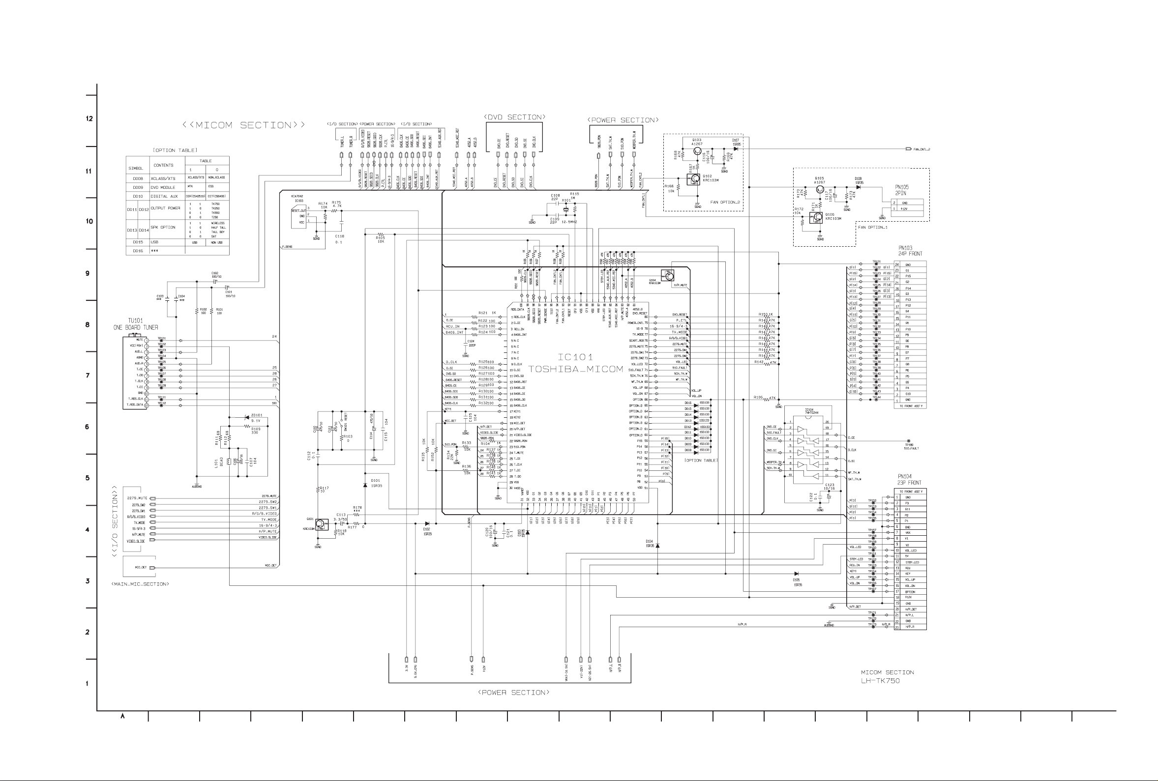
3. MICOM SCHEMATIC DIAGRAM
A B C D E F G H I J K L M N O P Q R ST
Page 15
2-14 2-15
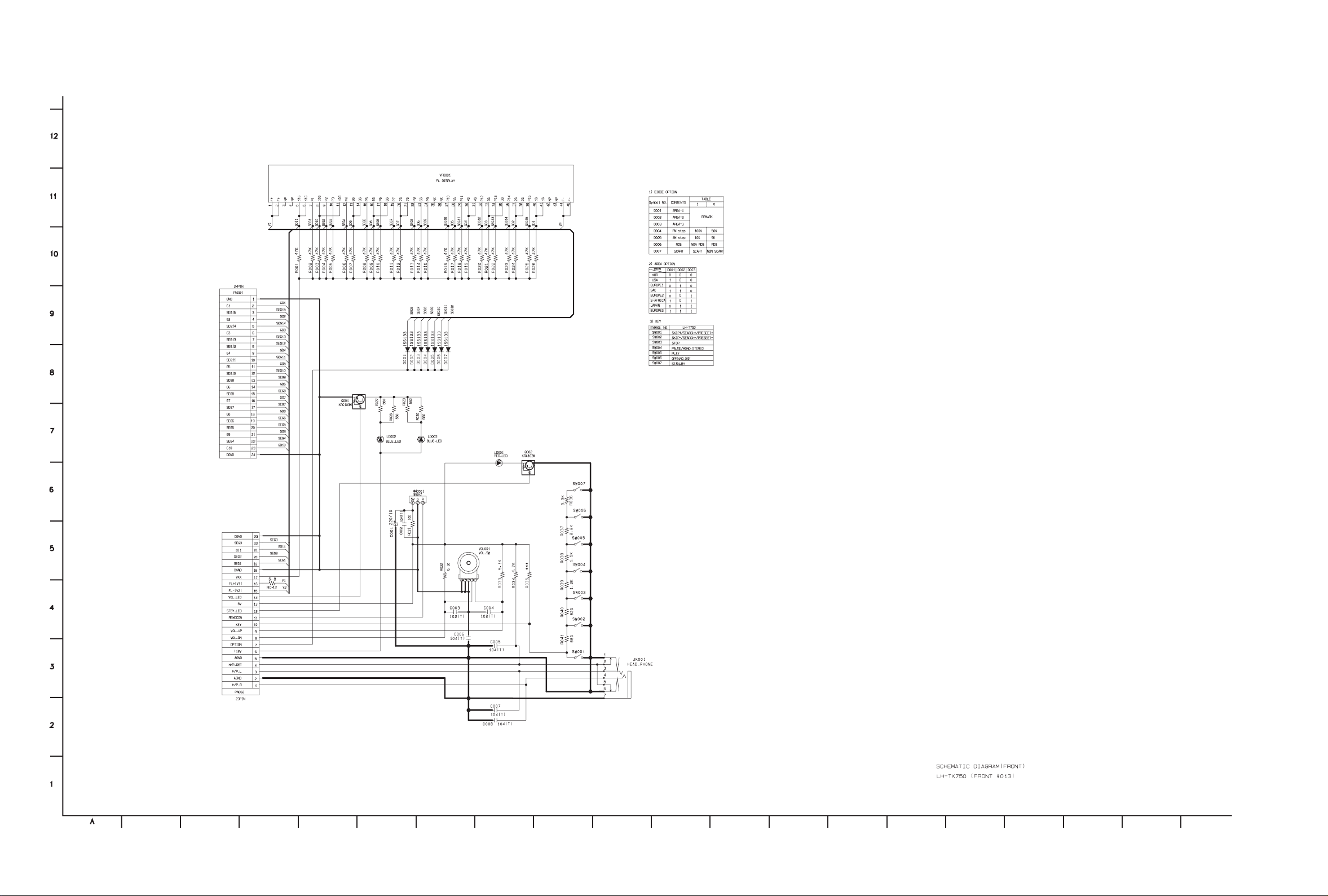
4. FRONT SCHEMATIC DIAGRAM
A B C D E F G H I J K L M N O P Q R ST
Page 16

2-16 2-17
5. DSP& SCHEMATIC DIAGRAM
A B C D E F G H I J K L M N O P Q R ST
Page 17

2-18 2-19
6. I/O SCHEMATIC DIAGRAM
A B C D E F G H I J K L M N O P Q R ST
Page 18
2-20 2-21
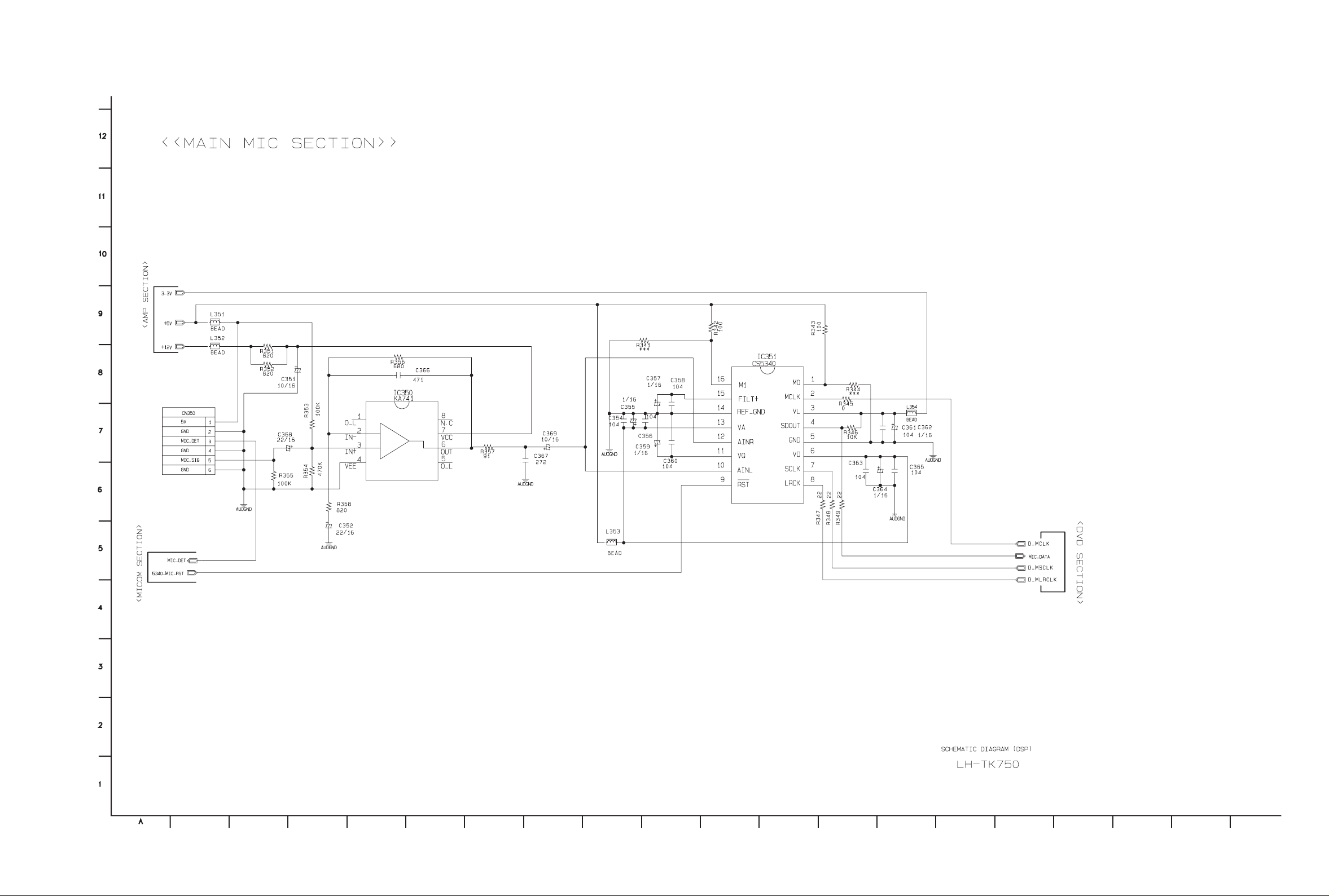
7. MAIN MIC SCHEMATIC DIAGRAM
A B C D E F G H I J K L M N O P Q R ST
Page 19

2-22 2-23
PRINTED CIRCUIT BOARD DIAGRAMS
1. MAIN/DVD P.C. BOARD DIAGRAM ( TOP VIEW )
Page 20
2-24 2-25
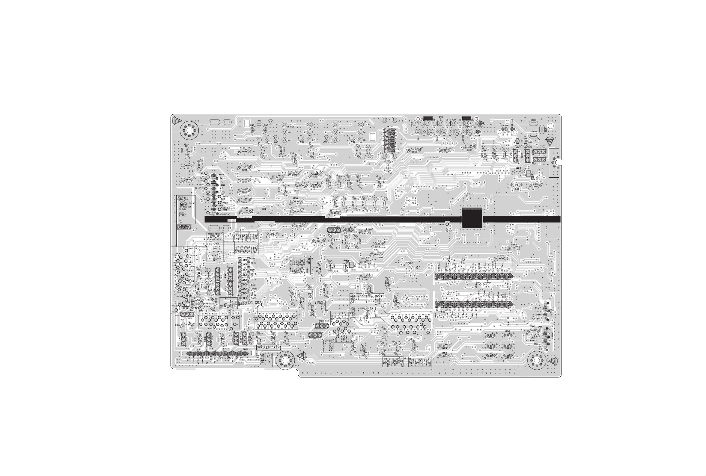
2. MAIN/DVD P.C. BOARD DIAGRAM ( BOTTOM VIEW )
6870R7505AC
Page 21

2-26 2-27
3. FRONT MIC P.C. BOARD
6870R7507AA
Page 22

2-28 2-29
4. SMPS P.C. BOARD
LOCATION GUIDE
NOTES) Warning
NOTES) Parts that are shaded are critical
NOTES) With respect to risk of fire or
NOTES) electricial shock.
5. MIC P.C. BOARD
( 5 TOOL )
LOCATION GUIDE
NOTES) Warning
NOTES) Parts that are shaded are critical
NOTES) With respect to risk of fire or
NOTES) electricial shock.
( 7 TOOL )
( TOP VIEW )
( BOTTOM VIEW )
Page 23
2-30 2-31
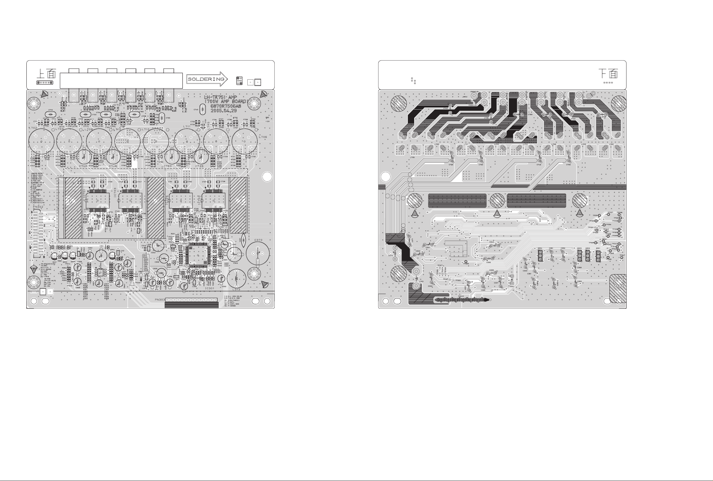
6. AMP P.C. BOARD
( TOP VIEW ) ( BOTTOM VIEW )
Page 24
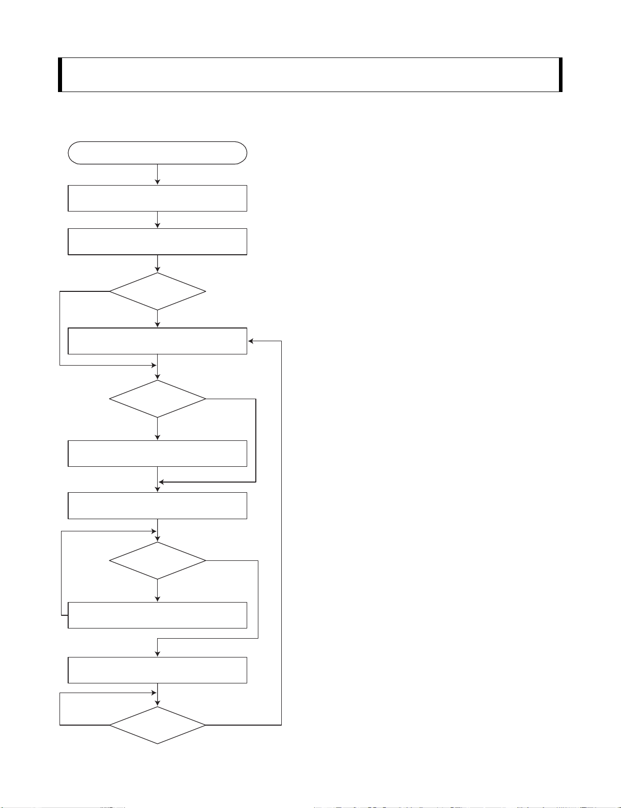
3-1
ELECTRICAL TROUBLESHOOTING GUIDE
1. System operation flow
SECTION 3. DVD & AMP PART
Power On
1. 8082 initializes SERVO, DSP & RISC registers
2. Write RISC code to SDRAM
3. Reset RISC
Show LOGO
Yes
SLED Moves to Inner Position
1. Judge whether have disc and disc type
2. Jump to related disc reading procedure
Tray Closed?
No
Tray Close to Closed position
SLED at Inner
Side?
No
Recieve
OPEN/ CLOSE
Key?
Yes
No
1. Execute Pressed Key & IR Key
2. Systemoperati on Routi ne Loop
1. Stop Playback & Open Tray
2. Display tray open message & LOGO
No
Receive
CLOSE Key?
Yes
Page 25

3-2
2. Test & debug flow
TEST
Check the
AC Vol tage
Power PCBA (110V
or 220V)
Yes
Switch on the Power PCBA
Is the
DC Voltage
outputs OK? (-44V, -22V,
-26.5V, ±12V, 5.6V, 3.3V,
5V, 7V, 8V)
Yes
Are 3.3V and 5V DC
outputs normal on main
PCBA?
Yes
Update
FLASH
successfully?
No
No
No
No
Check the POWER PART
Check the POWER PART
Check the regulators or diode.
1. Check 27MHz system clock.
2. Check systemreset circuit.
3. Check FLASH R/Wenable signal PRD,
RWR.
4. Check FLASH Memory related circuit.
Yes
Replace FLASH
A
Page 26

3-3
A
, 115.
Page 27

3-4
B
1.
2.
Page 28

3-5
C
ES6698.
ES6698.
ES6698.
Page 29

3-6
D
Page 30

3-7
E
PWM IC
received correct data
stream?
Normal
PWM IC out?(IC301)
Check Digital Amp circuit
(IC701, IC702, IC703, IC704)
Check connection between
IC300 ABCK, ALRCK,
ASDAT
Check the related circuit of
PWM.(Check Audio out
Pins52, 54, 55, 59,62, 68
Page 31

3-8
3. AUDIO µ-COM Circuit(DVD & AMP)
YES
Does CD/DVD appear
at FLD?
Does AV1, TV Audio, AV1 opt.
and FM 87.5 appear at FLD
OK
Does Loading appear
at FLD?
POWER ON
YES NO
YES
Does no Disc or Time
appear at FLD?
NO YES
NO
NO
NO
NO
NO
NO
Does it appear DVD Error
at FLD?
Refer to SMPS.
Refer to oscillator Circuit.
Check IC101 Reset
Waveform.
Check 3.3V line.
Check Power section
Circuit.
NO
Check power part of Main
B/D.
Check oscillator of X101.
Check if IC101 Pin80
is high.
Check if IC101 Pin32, 51,
80 are high(5V).
Check if IC101 Pin96
is high.
Replace IC101.
NO
NO
Check if DVD an Audio
Micom Insert is OK.
Check Power.
YES
Check DVD Module.
YES
Check SMPS.
YES YES
YES
YES
YES
YES
YES
Page 32

3-9
DETAILS AND WAVEFORMS ON SYSTEM TEST AND DEBUGGING
1. SYSTEM 27MHz CLOCK,RESET,FLASH R/W SIGNAL
1) ES6698FD main clock is at 27MHz(X501)
3.8V, 27MHz
FIG 1-1
2) ES6698FD reset is high active.
PWR_CTL(SYSTEM µ-COM)
IC501 PIN83)
5.2VA
Power Cord in
M_RESET(IC501 PIN 207)
URST(IC501 PIN 188)
FIG 1-2
Page 33

3-10
2. SDRAM CLOCK
1) ES6698FD main clock is at 27MHz(X501)
(IC503 PIN 38)
DCLK = 93MHz, Vp-p=2.2, Vmax=2.7V
FIG 2-1
3) Flash R/W enable signal during download(Downloading)
FRD(IC500 PIN 28)
FWR(IC500 PIN 11)
FIG 1-4
Page 34

3-11
3. TRAY OPEN/CLOSE SIGNAL
1) Tray open/close waveform
OPEN((PDM03 PIN7)
CLOSE(PDM03 PIN8)
TROPEN(IC402 PIN 4)
TRCLOSE(IC402 PIN 5)
FIG 3-1
2) Tray close waveform
OPEN((PDM03 PIN7)
CLOSE(PDM03 PIN8)
TROPEN(IC402 PIN 4)
TRCLOSE(IC402 PIN 5)
FIG 3-2
Page 35

3-12
4. SLED CONTROL RELATED SIGNAL (NO DISC CONDITION)
FMSO(2.0V/1.4V/1.0V)
(IC501 PIN 19)
STBY(5V) – (IC401 PIN 50)
SL+(4.7V/3.6V/1.9V)
(IC404 PIN 12)
SL-(5.3V/3.7V/2.5V)
(IC404 PIN 11)
FIG 4-1
3) Tray open waveform
OPEN(PDM03 PIN7)
CLOSE(PDM03 PIN8)
TROPEN(IC402 PIN 4)
TRCLOSE(IC402 PIN 5)
FIG 3-3
Page 36

3-13
5. LENS CONTROL RELATED SIGNAL(NO DISC CONDITION)
FOSO(1.5V/1.4V/1.3V)
(IC501 PIN 12)
F+(4.0V/3.6V/3.2V)
(IC404 PIN 14)
F-(4.0V/3.6V/3.2V)
(IC404 PIN 13)
FIG 5-1
6. LASER POWER CONTROL RELATED SIGNAL(NO DISC CONDITION)
MDI1(0V/180mV)
(IC401 PIN 26)
LD01(5.0V//3.5V)
IC401 PIN 20)
LD02(5.0V/3.6V)
(IC401 PIN 21)
FIG 6-1
Page 37

3-14
F+(IC404 PIN 14)
FE(IC401 PIN 40)
RFL(IC401 PIN 19)
FIG 7-2 (DVD)
7. DISC TYPE JUDGEMENT WAVEFORMS
F+(IC404 PIN 14)
FE(IC401 PIN 40)
RFL(IC401 PIN 19)
FIG 7-1 (DVD)
Page 38

3-15
F+(IC404 PIN 14)
FE(IC401 PIN 40)
RFL(IC401 PIN 19)
FIG 7-3 (CD)
F+(IC404 PIN 14)
FE(IC401 PIN 40)
RFL(IC401 PIN 19)
FIG 7-4 (CD)
Page 39

3-16
FE(IC401 PIN 40)
FOSO(IC501 PIN12)
F+(IC404 PIN 14)
F-(IC404 PIN 13)
FIG 8-2 (CD)
8. FOCUS ON WAVEFORMS
FE(IC401 PIN 40)
FOSO(IC501 PIN12)
F+(IC404 PIN 14)
F-(IC404 PIN 13)
FIG 8-1 (DVD)
Page 40

3-17
9. SPINDLE CONTROL WAVEFORMS (NO DISC CONDITION)
DMSO(1.4V/1.8V)
(IC501 PIN 18)
SP-(3.6V/2.4V)
(IC404 PIN 18)
SP+(3.6V/4.8V)
(IC404 PIN 17)
FIG 9-1
10. TRACKING CONTROL RELATED SIGNAL(System checking)
TE(IC401 PIN 39)
TRSO(IC501 PIN 13)
T-(IC404 PIN 16)
T+(IC404 PIN 15)
FIG 10-1(DVD)
Page 41

3-18
11. RF WAVEFORM
RFOP(2.3V/1.1V)
(IC401 PIN 55)
RFON(0.8V/2.0V)
(IC401 PIN 57)
FIG 11-1
TE(IC401 PIN 39)
TRSO(IC501 PIN 13)
T-(IC404 PIN 16)
T+(IC404 PIN 15)
FIG 10-2(CD)
Page 42

3-19
12. ES6698FD VIDEO OUTPUT WAVEFORMS
1) Full colorbar signal(COMPOSIT)
(IC501 PIN 110)
FIG 12-1
2) Y
(IC501 PIN 113)
FIG 12-2
Page 43

3-20
1) Audio L/R
FIG 13-1
13. AUDIO OUTPUT FROM PWM IC
(IC301 PIN 68, 49)
2) Audio related Signal
ASDAT0(IC501 PIN 117)
ABCK(IC501 PIN 123)
ALRCK(IC501 PIN 116)
ASDATA3
FIG 13-2
Page 44

3-21
1)
• R310 → TP301
or
R311 TP302
2)
• R320 → TP311
or
R321 TP312
3)
• R312 → TP303
or
R313 TP304
4)
• R318 → TP307
or
R319 TP308
5)
• R314 → TP305
or
R315 TP304
6)
• R318 → TP309
or
R319 TP310
14. DVD & AMP WAVEFORMS
Page 45

Page 46

A B C D E F G H I J K L M N O P Q R ST
3-22 3-23
DVD PART SCHEMATIC DIAGRAMS
1. DVD MPEG & DSP SCHEMATIC DIAGRAM
Page 47

A B C D E F G H I J K L M N O P Q R ST
3-24 3-25
2. RF & SERVO SCHEMATIC DIAGRAM
Page 48

3. FRONT MIC SCHEMATIC DIAGRAM(KARAOKE MODEL ONLY)
A B C D E F G H I J K L M N O P Q R ST
3-26 3-27
Page 49

3-28 3-29
4. USB CONTROLLER SCHEMATIC DIAGRAM
A B C D E F G H I J K L M N O P Q R ST
Page 50

5. AMP SCHEMATIC DIAGRAM ( 5TOOL )
A B C D E F G H I J K L M N O P Q R ST
3-30 3-31
Page 51

6. AMP SCHEMATIC DIAGRAM ( 7TOOL )
A B C D E F G H I J K L M N O P Q R ST
3-32 3-33
Page 52

• CABINET AND MAIN FRAME SECTION
4-1 4-2
SECTION 4. EXPLODED VIEWS
OPTIONAL PART
NOTES) THE EXCLAMATION POINT WITHIN AN
EQUILATERAL TRIANGLE IS INTENDED
TO ALERT THE SERVICE PERSONNEL
TO THE PRESENCE OF IMPORTANT
SAFETY INFORMATION IN SERVICE
LITERATURE.
452
JACK OPTION
A53
274
A50
452
283
A26
275
463
A46
463
463
463
250
463
463
A43
279
261
261
463
465
A45
A47
300
A44
261
Page 53

• DECK MECHANISM EXPLODED VIEW
4-3 4-4
012
019
A26
013
017
439
014
435
015
018
015B
015A
012
440
016
030
001
002
A01
003
A02
020
432
012A
026
A03
036
439
025
010
024
431
435
012A
021
430
035A
035
Page 54

4-5
• Packing Accessory Section
827
MICRO PHONE
826
FILTER(CIRC)
808
BATTERY
900
REMOCON
803
PACKING, CASING
OPTIONAL PART
811
PLUG ASS'Y 1WAY(YELLOW)
824
ANTENNA LOOP(AM)
825
ANTENNA (FM)
INSTRUCTION ASSEMBLY
801
828
AC ADAPTOR
PACKING, CASING
803
804
BAG
802
BOX
Page 55

Page 56

5-1
SECTION 5. SPEAKER SECTION
• CENTER SPEAKER
MODEL : LHS-55TBC
A70
752
750
751
754
OPTIONAL
PARTS
LHS-75TBC
XHS-75TBS
ONLY
752
752
755
753
758
757
751
Page 57

5-2
• FRONT/REAR SPEAKER
MODEL : LHS-55TBS
A80
854
A80A
863
862
850
851
OPTIONAL
PARTS
LHS-75TBS
XHS-75TBS
ONLY
852
853
855
857
856
850
858
851
859
860
861
864
865
867
866
Page 58

5-3
• SUB WOOFER SPEAKER
MODEL : LHS-55TBW
953
954
952
951
A90
956
950
Page 59

5-4
• MODEL : TRANSMITTER (ACC55T)
A300
380
(With LENS)
382
A80M
A80S
384
480
Page 60

5-5
• MODEL : RECEIVER(ACC55R)
394
398
A330
390
*NSP
492
A81A
A81M
392
*NSP
A81S
396
491
Page 61

5-6
< REFERENCE >
5-1. TRANSMITTER(TX) ELECTRICAL
5-1-1. TX MODULE BLOCK DIAGRAM
IA8
(BASEBAND IC)
3.3V
2
I C
ANT
TX ON
uPG2214
RX ON
RF IN(CH)
(SWITCH IC)
RX
AL2212
TX
(RF IC)
(EEPROM)
AT24C64AN
2
I C
OSC(44MHz)
RF OUT
(FILTER)
MFG22B2450
2.8V 3.3V
3.3V
POWER POWER
Page 62

5-7
5-1-2. TX SUB BLOCK DIAGRAM
TX MODULE
LED SWITCH
AUDIO IN
POWER - 7V REGULATOR - 5V
OP AMP
AUDIO
DVD
Page 63

5-8
5-1-3. TX MODULE SCHEMATIC DIAGRAM_1
Page 64

5-9
5-1-4. TX MODULE SCHEMATIC DIAGRAM_2
Page 65

5-10
5-1-5. TX MODULE SCHEMATIC DIAGRAM_3
Page 66

5-11
5-1-6. TX SUB SCHEMATIC DIAGRAM
Page 67

5-12
5-1-7. TX MODULE PRINTED CIRCUITED DIAGRAM(UPPER SIDE)
Page 68

5-13
5-1-8. TX MODULE PRINTED CIRCUITED DIAGRAM(LOWER SIDE)
Page 69

5-14
5-1-9. TX PRINTED CIRCUITED DIAGRAM
Page 70

5-15
5-2. RECEIVER(RX) ELECTRICAL
5-2-1. RX MODULE BLOCK DIAGRAM
SMPS
I2S(AUDIO OUT) POWER CONTROL
SWITCH
LED AMP
IA8
(BASEBAND IC)
RX
I2C
POWER
3.3V
(EEPROM)
AT24C64AN
ANT
RF IN
(RF IC)
AL2212
2.8V I2C 3.3V
POWER OSC(44MHz)
Page 71

5-16
5-2-2. RX MODULE SCHEMATIC DIAGRAM_1
Page 72

5-17
5-2-3. RX MODULE SCHEMATIC DIAGRAM_2
Page 73

5-18
5-2-4. RX MODULE SCHEMATIC DIAGRAM_3
Page 74

5-19
+
5-2-5. RX AMP SCHEMATIC DIAGRAM_1
CHB-
L1 15UH
1 2
RADIAL13.5DIA
1 2
1234567891011
123456789
RADIAL13.5DIA
L3 15UH
R5100000-1210
5%
C17
OUTPUT
C19
R
100NF
X7
C18
680PF
NPO
1000PF
R
X7
NPO
C41
NC
C27
1000PF
ChassisG nd
FILM
C23
470NF
R
X7
6.2
5%
EIA1210
R8
R7100000-1210
C26
6.2
R
100NF
X7
5%
EIA1210
5%
C21
100NF
R6
CHA+
NPO
R
C28
100NF
X7
L4 15UH
1 2
RADIAL13.5DIA
R
C25
680PF
X7
12
J1
101112
1000PF
NPO
C13
100NF
5%
R
X7
C15
CHB+
L2 15UH
1 2
RADIAL13.5DIA
R
680PF
X7
NPO
C40
NC
C2
1000PF
NPO
R
C6
100NF
X7
R
R2
6.2
EIA1210
C1
100NF
X7
R1100000-1210
5%
C12
ChassisG nd
FILM
C8
470NF
R
C11
100NF
X7
R3
6.2
5%
5%
EIA1210
R
C9
680PF
X7
R4100000-1210
R
VCC2N
VREG2
50VDC
PGND2N
INRB
DDX2B
C14 100NF
PGND2P
INRA
313233
DDX2A
VCC2P
INLB
DDX1B
X7
OUTPR
INLA
DDX1A
OUTPR
TWARN
282930
TWARN
OUTNL
FAULT
27
FAULT
C16 1uF
OUTNL
TRI-STATE
25
26
E
TRISTAT
EAPD
VCC1N
PWRDN
+
50VDC
C10 1uF
C5 1000UF
4V
+3
2345678910111213141516171819
OUTNR
OUTNR
U1
VSIG GNDREF
36 1
VSIG
35
X7R
EIA0805
C42
100NF
34
100NF
X7R
VREG2
C43
EIA0805
VREG1
50VDC
PGND1N
CONFIG
24
4V
+3
23
3.3V
C20 100NF
PGND1P
VL
22
VCC1P
VREG1
C44
R
X7
OUTPL
VREG1
21
C45 100NF
100NF
20
EIA0805
X7R
X7R
EIA0805
OUTPL
GNDR1
NC
GNDREF
DDX-2102
HeatSink
03
ChassisG nd
R9
220
0000-06
Page 75

5-20
5-2-6. RX AMP SCHEMATIC DIAGRAM_2
+34V+3.3V
123
4
J2
R11
10K
03
0000-06
C39
10nF
3
U3
1
89
KIA-7029
SOT-
Out
GND
2
Vcc
4
3
U2
TO-252-
BA33BC0FP
POWER
C35
22uF
10V
EIA3528_B
+
C36
Y5V
100NF
EIA0603
Vout
3
D
NC
GN
2
Vin
1
C38
100UF
16V
100UF-ELEC-16V-RADIAL
+
+3.3V
+3.3V
3
R13NS0000-060
03
R12NS0000-06
LRCLK
SDI_12
MCLK
BICLK
03
R24NS0000-06
03
R23NS0000-06
03
R22NS0000-06
3
R21NS0000-060
SDA
RESET
SCL
+5V
C37
Y5V
100NF
EIA0603
**Note: R20 can be
05
R2000000-08
replaced w ith an
EIA0805 ferr ite bead
if needed fo r EMI**
SDATA
123456789
J3
LRCK
MCLK
BICLK
SCL
SDA RESET
RESET
10
Page 76

5-21
5-2-7. RX AMP SCHEMATIC DIAGRAM_3
PWDN
C48
100NF
E
FAULT
26
FAULT
DDX1B
TRISTAT
24
25
TRISTATE
OCDETECT
DDX2A
DDX2B
TWARN
27
28
GND
TWARN
U4
SA
DDX1A
123456789
EAPD
23
EAPD
RESET
22
DDX3A
SCL
21
DDX3B
SDA
20
Y5V
+3.3V
C47
22UF
10VDC
+
C46
100NF
Y5V
17
18
19
VDD
VDD
PWDN
GND
PLL_FILTER
XTI
1011121314 15
EIA0603
EIA3528_B
EIA0603
16
GND
BICKI
GNDA
VDDA
BICLK
SDI_12 LRCKI
LRCLK
DDX-2001
VDDA
C31
+
C29
Y5V
100NF
22UF
10VDC
GNDA
EIA0603
EIA3528_A
EIA0603
100PF
NPO
EIA0603
EIA0603
1200PF
X7R
NPO
C33
C32
C34
220PF
3
R10
3.40K
0000-060
PLL
DDX1A
DDX1B
DDX2A
DDX2B
RESET
SCL
SDA
PLL
MCLK
GNDA
VDDA
SDI_12
12
L5
EIA0805
600 ohm@100mhz
C30
+3.3V
12
L6
600 ohm@100mhz
Y5V
100NF
EIA0603
EIA0805
Page 77

5-22
5-2-8. RX MODULE + AMP SCHEMATIC DIAGRAM
Page 78

5-23
5-2-9. RX SMPS(POWER) SCHEMATIC DIAGRAM
Page 79

5-24
5-2-10. RX MODULE PRINTED CIRCUITED DIAGRAM(UPPER SIDE)
Page 80

5-25
5-2-11. RX MODULE PRINTED CIRCUITED DIAGRAM(LOWER SIDE)
Page 81

5-26
5-2-12. AMP PRINTED CIRCUITED DIAGRAM(UPPER SIDE)
Page 82

5-27
5-2-14. RX SMPS(POWER) PRINTED CIRCUITED DIAGRAM(COMPONENT SIDE)
Page 83

 Loading...