

LG A290 SERVICE MANUAL

Internal Use Only
Service Manual
LG-A290
Date: January, 2012 / Issue 1.0

- 2 -
LGE Internal Use Only Copyright © 2012 LG Electronics. Inc. All right reserved.
Only for training and service purposes
Table Of Contents
1. INTRODUCTION ............................................................... 3
1.1 Purpose ................................................................................................3
1.2 Regulatory Information .................................................................3
1.3 Abbreviations.....................................................................................5
2. SYSTEM SPECIFICATION .................................................7
2.1 H/W Features ......................................................................................7
2.2 Technical Specification ...................................................................9
3. TECHNICAL BRIEF ..........................................................14
3.1 Digital Main Processor .................................................................14
3.2 Power Management .................................................................... 19
3.3 FEM with integrated Power Amplifier Module
(SKY77550, U400) .......................................................................... 24
3.4 Clocks ................................................................................................. 26
3.5 RFSYS of MT6253 (U101) ............................................................ 28
3.6 MEMORY(PF38F5060M0Y3DK, U100 ) ..................................30
3.7 BT & FM Module(MT6626, U401) ........................................... 34
3.8 SIM Card Interface ......................................................................... 38
3.9 Micro-SD Card Interface ............................................................. 41
3.10 LCD Interface ................................................................................ 44
3.11 Battery Charger Interface / MUIC ......................................... 46
3.12 Keypad Interface .........................................................................48
3.13 Audio Front-End ..........................................................................51
3.14 Camera Interface ......................................................................... 55
3.15 KEY BACLKLIGHT LED Interface ............................................ 57
3.16 Vibrator Interface ........................................................................ 58
3.17 Torch LED Interface .................................................................... 59
4.12 SIM1 Card Interface Trouble ................................................... 90
4.13 SIM2 Card Interface Trouble .................................................. 92
4.14 SIM3 Card Interface Trouble .................................................. 94
4.15 KEY backlight Trouble ............................................................... 96
4.16 Torch Trouble ................................................................................ 98
4.17 Micro SD Trouble ......................................................................100
4.18 Bluetooth Trouble ....................................................................102
4.19 FM Radio Trouble ....................................................................104
5. DOWNLOAD .................................................................106
6. BLOCK DIAGRAM .........................................................119
7. Circuit Diagram ...........................................................120
8 BGA PIN MAP ................................................................124
9. PCB LAYOUT .................................................................126
10. ENGINEERING MODE ................................................128
11 RF CALIBRATION ........................................................129
11.1 Configuration of Tachyon .....................................................129
11.2 How to use Tachyon .................................................................131
12 EXPLODED VIEW & REPLACEMENT PART LIST ........133
12.1 EXPLODED VIEW ........................................................................133
12.2 ReplacementParts ....................................................................134
12.3 Accessory .....................................................................................151
4. TROUBLE SHOOTING ....................................................60
4.1 RF Component .............................................................................. 60
4.2 RX Trouble ....................................................................................... 61
4.3 TX Trouble ........................................................................................ 65
4.4 Power On Trouble .......................................................................... 69
4.6 Vibrator Trouble ............................................................................. 74
4.7 LCD Trouble ..................................................................................... 76
4.8 Camera Trouble .............................................................................. 79
4.9 Speaker/ Receiver Trouble ......................................................... 83
4.10 3.5φ Headset Trouble ................................................................ 85
4.11 Microphone Trouble ..................................................................88

1. INTRODUCTION
1. INTRODUCTION
1.1 Purpose
This manual provides the information necessary to repair, calibration, description and download the features of this
model.
1.2 Regulatory Information
A. Security
Toll fraud, the unauthorized use of telecommunications system by an unauthorized part (for example, persons other
than your company’s employees, agents, subcontractors, or person working on your company’s behalf) can result in
substantial additional charges for your telecommunications services. System users are responsible for the security of
own system. There are may be risks of toll fraud associated with your telecommunications system. System users are
responsible for programming and configuring the equipment to prevent unauthorized use. The manufacturer does
not warrant that this product is immune from the above case but will prevent unauthorized use of common-carrier
telecommunication service of facilities accessed through or connected to it.
The manufacturer will not be responsible for any charges that result from such unauthorized use.
B. Incidence of Harm
If a telephone company determines that the equipment provided to customer is faulty and possibly causing harm or
interruption in service to the telephone network, it should disconnect telephone service until repair can be done. A
telephone company may temporarily disconnect service as long as repair is not done.
C. Changes in Service
A local telephone company may make changes in its communications facilities or procedure. If these changes could
reasonably be expected to affect the use of the this phone or compatibility with the network, the telephone company is
required to give advanced written notice to the user, allowing the user to take appropriate steps to maintain telephone
service.
D. Maintenance Limitations
Maintenance limitations on this model must be performed only by the manufacturer or its authorized agent. The user
may not make any changes and/or repairs expect as specifically noted in this manual. Therefore, note that unauthorized
alternations or repair may affect the regulatory status of the system and may void any remaining warranty.
LGE Internal Use Only Copyright © 2012 LG Electronics. Inc. All right reserved.
- 3 -
Only for training and service purposes
- 4 -
LGE Internal Use Only Copyright © 2012 LG Electronics. Inc. All right reserved.
Only for training and service purposes
1. INTRODUCTION
E. Notice of Radiated Emissions
This model complies with rules regarding radiation and radio frequency emission as defined by local regulatory agencies.
In accordance with these agencies, you may be required to provide information such as the following to the end user.
F. Pictures
The pictures in this manual are for illustrative purposes only; your actual hardware may look slightly different.
G. Interference and Attenuation
Phone may interfere with sensitive laboratory equipment, medical equipment, etc.Interference from unsuppressed
engines or electric motors may cause problems.
H. Electrostatic Sensitive Devices
ATTENTION
Boards, which contain Electrostatic Sensitive Device (ESD), are indicated by the sign.
Following information is ESD handling:
Service personnel should ground themselves by using a wrist strap when exchange system boards.
•
When repairs are made to a system board, they should spread the floor with anti-static mat which is also grounded.
•
Use a suitable, grounded soldering iron.
•
Keep sensitive parts in these protective packages until these are used.
•
When returning system boards or parts like EEPROM to the factory, use the protective package as described.
•
1.3 Abbreviations
For the purposes of this manual, following abbreviations apply:
APC Automatic Power Control
BB Baseband
BER Bit Error Ratio
CC-CV Constant Current – Constant Voltage
DAC Digital to Analog Converter
DCS Digital Communication System
1. INTRODUCTION
dBm dB relative to 1 milli watt
DSP Digital Signal Processing
EEPROM Electrical Erasable Programmable Read-Only Memory
ESD Electrostatic Discharge
FPCB Flexible Printed Circuit Board
GMSK Gaussian Minimum Shift Keying
GPIB General Purpose Interface Bus
GSM Global System for Mobile Communications
IPUI International Portable User Identity
IF Intermediate Frequency
LCD Liquid Crystal Display
LDO Low Drop Output
LED Light Emitting Diode
OPLL Offset Phase Locked Loop
PAM Power Amplifier Module
LGE Internal Use Only Copyright © 2012 LG Electronics. Inc. All right reserved.
- 5 -
Only for training and service purposes
PCB Printed Circuit Board
PGA Programmable Gain Amplifier
PLL Phase Locked Loop
PSTN Public Switched Telephone Network
RF Radio Frequency
RLR Receiving Loudness Rating
RMS Root Mean Square
RTC Real Time Clock
1. INTRODUCTION
SAW Surface Acoustic Wave
SIM Subscriber Identity Module
SLR Sending Loudness Rating
SRAM Static Random Access Memory
PSRAM Pseudo SRAM
STMR Side Tone Masking Rating
TA Travel Adapter
TDD Time Division Duplex
TDMA Time Division Multiple Access
UART Universal Asynchronous Receiver/Transmitter
VCO Voltage Controlled Oscillator
VCTCXO Voltage Control Temperature Compensated Crystal Oscillator
WAP Wireless Application Protocol
LGE Internal Use Only Copyright © 2012 LG Electronics. Inc. All right reserved.
- 6 -
Only for training and service purposes
2. SYSTEM SPECIFICATION
2.1 H/W Features
Item Feature Comment
Standard Battery Lithium Ion, 3.7V 1500mAh
Stand by TIME >450 hr., Min.@PP9
Stand by time >500 hr., Min.@PP5
>6.0hr., Min.@GSM900, PL=5
Talk time
Charging time Approx. 3 hours 30 min.
>14.0 hr., Min.@GSM900, PL=13
>8 hr., Min.@DCS, PL=0
>14 hr., Min.@DCS, PL=9
2. PERFORMANCE
RX Sensitivity GSM, EGSM: -109dBm, DCS: -109dBm
TX output power
GPRS compatibility Class 10
SIM card type 3V Small
Display MAIN : TFT 176 × 220(QCIF) pixel 262K Color
Status Indicator
ANT Internal
EAR Phone Jack Yes(3.5Ø)
PC Synchronization Yes
Speech coding EFR/FR/HR
GSM, EGSM: 32.3dBm(Level 5),
DCS , PCS: 29.5dBm(Level 0)
KEY TOTAL 22EA
Hard icons. Key Pad
Numeric(12EA : 0 ~ 9, #, *) Navigation Key OK Key(5EA)
Menu Key, Clear Key, Send Key, End Key,
SIM Switch Key(5EA)
Data and Fax Yes
Vibrator Yes
Loud Speaker Yes
Voice Recoding Yes
LGE Internal Use Only Copyright © 2012 LG Electronics. Inc. All right reserved.
- 7 -
Only for training and service purposes

- 8 -
LGE Internal Use Only Copyright © 2012 LG Electronics. Inc. All right reserved.
Only for training and service purposes
2. PERFORMANCE
Item Feature Comment
Microphone Yes
Speaker/Receiver 18 x 12 Speaker/Receiver
Travel Adapter Yes
MIDI SW MIDI (Mono SPK)
Camera 1.3M
Bluetooth / FM Radio Bluetooth version 2.1 / 76~108MHz supported

2.2 Technical Specification
Item Description Specification
2. PERFORMANCE
GSM850
TX: 824 ~ 849 MHz
RX: 869 ~ 894 MHz
DCS
1 Frequency Band
2 Phase Error
3 Frequency Error < 0.1ppm
TX: 1710 ~ 1785 MHz
RX: 1805 ~ 1880 MHz
PCS
TX: 1850 ~ 1910 MHz
RX: 1930 ~ 1990 MHz
RMS < 5 degrees
Peak < 20 degrees
GSM850 / EGSM
Level Power Toler. Level Power Toler.
5 33 dBm ±2dB 13 17 dBm ±3dB
6 31 dBm ±3dB 14 15 dBm ±3dB
7 29 dBm ±3dB 15 13 dBm ±3dB
8 27 dBm ±3dB 16 11 dBm ±5dB
EGSM
TX: 880 ~ 915MHz
RX: 925 ~ 960 MHz
4 Power Level
9 25 dBm ±3dB 17 9 dBm ±5dB
10 23 dBm ±3dB 18 7 dBm ±5dB
11 21 dBm ±3dB 19 5 dBm ±5dB
12 19 dBm ±3dB
DCS / PCS
Level Power Toler. Level Power Toler.
0 30 dBm ±2dB 8 14 dBm ±3dB
1 28 dBm ±3dB 9 12 dBm ±4dB
2 26 dBm ±3dB 10 10 dBm ±4dB
3 24 dBm ±3dB 11 8 dBm ±4dB
4 22 dBm ±3dB 12 6 dBm ±4dB
5 20 dBm ±3dB 13 4 dBm ±4dB
6 18 dBm ±3dB 14 2 dBm ±5dB
7 16 dBm ±3dB 15 0 dBm ±5dB
LGE Internal Use Only Copyright © 2012 LG Electronics. Inc. All right reserved.
- 9 -
Only for training and service purposes
- 10 -
LGE Internal Use Only Copyright © 2012 LG Electronics. Inc. All right reserved.
Only for training and service purposes
2. PERFORMANCE
Item Description Specification
GSM850 / EGSM
Offset from Carrier (kHz). Max. dBc
100 +0.5
200 -30
250 -33
400 -60
600 ~ <1,200 -60
1,200 ~ <1,800 -60
Output RF Spectrum
5
(due to modulation
1,800 ~ <3,000 -63
3,000 ~ <6,000 -65
6,000 -71
DCS/ PCS
Offset from Carrier (kHz). Max. dBc
100 +0.5
200 -30
250 -33
400 -60
600 ~ <1,200 -60
1,200 ~ <1,800 -60
1,800 ~ <3,000 -65
3,000 ~ <6,000 -65
6,000 -73
GSM850 / EGSM
Offset from Carrier (kHz). Max. dBm
Output RF Spectrum
6
(due to switching transient)
400
600 -21
1,200
1,800
-19
-21
-24
Item Description Specification
DCS/ PCS
Offset from Carrier (kHz). Max. dBm
2. PERFORMANCE
Output RF Spectrum
6
(due to switching transient)
7 Spurious Emissions Conduction, Emission Status
GSM850, EGSM
8 Bit Error Ratio
9 RX Level Report Accuracy ± 3 dB
10 SLR 15±3 dB
BER (Class II) < 2.439% @-102 dBm
DCS,PCS
BER (Class II) < 2.439% @-102 dBm
400 -22
600 -24
1,200 -24
1,800 -27
Frequency (Hz) Max.(dB) Min.(dB)
100 -12 -
200 0 -
300 0 -12
11 Sending Response
12 RLR(Norminal) 4± 3 dB
LGE Internal Use Only Copyright © 2012 LG Electronics. Inc. All right reserved.
1,000 0 -6
2,000 4 -6
3,000 4 -6
3,400 4 -9
4,000 0 -
- 11 -
Only for training and service purposes
Item Description Specification
Frequency (Hz) Max.(dB) Min.(dB)
100 -6 -
200 2 -
300 2 -9
500 * *
13 Receiving Response
1,000 2 -7
3,000 2 *
3,400 2 -12
2. PERFORMANCE
4,000 2
* Mean that Adopt a straight line in between 300 Hz and 1,000 Hz to
be Max. level in the range.
14 STMR(Vol. Nominal) >17dB
15 Echo Loss >58dB
16 Idle Noise Sending < -64dBm0p
17 Idle Noise Receiving < -54dBm0P(Volume Max)
System frequency
18
(13 MHz) tolerance
19 32.768KHz tolerance ≤ 30 ppm
20 Ringer Volume
21
Charge Current
≤ 2.5 ppm
At least 58 dB spl under below conditions:
1. Ringer set as ringer.
2. Test distance set as 100 cm
Fast Charge : Typ. 600 mA
Slow Charge : Typ. 500mA
Total Charging Time : < Approx. 3 hours 30min.
LGE Internal Use Only Copyright © 2012 LG Electronics. Inc. All right reserved.
- 12 -
Only for training and service purposes

Item Description Specification
Bar Number Power
4 over -91dBm±2dBm
4 -> 3 -91dBm±2dBm
22
Antenna Display
3 -> 2 -99dBm±2dBm
2 -> 1 -103dBm±2dBm
1 -> 0 -105dBm±2dBm
Battery Bar Number Voltage
3 ≥ 3.75± 0.05 V
3. TECHNICAL BRIEF
23 Battery Indicator
Low Voltage Warning
24
( Blinking Bar)
Forced shut down
25
Voltage
Sustain RTC
26
without battery
27 Battery Type
28 Travel Charger
3 -> 2 3.75 ± 0.05 V
2 -> 1 3.65 ± 0.05 V
1 -> 0 3.5 ± 0.05 V
≤ 3.5 ± 0.05V (Call), every 1 minute
≤ 3.5 ± 0.05V (Standby), every 3 minute.
3.35 ± 0.05V
Over 1 min(Super Cap : Polyacene Capacitor 10uAh)
Li-Ion Battery
Standard Voltage = 3.7 V
Battery full charge voltage = 4.2 V
Capacity: 1500mAh
Switching-mode charger
Input: 90 ~ 264 V, 47/63 Hz
Output: 5.1 V, 700 mA
LGE Internal Use Only Copyright © 2012 LG Electronics. Inc. All right reserved.
- 13 -
Only for training and service purposes
- 14 -
LGE Internal Use Only Copyright © 2012 LG Electronics. Inc. All right reserved.
Only for training and service purposes
3. TECHNICAL BRIEF
3. TECHNICAL BRIEF
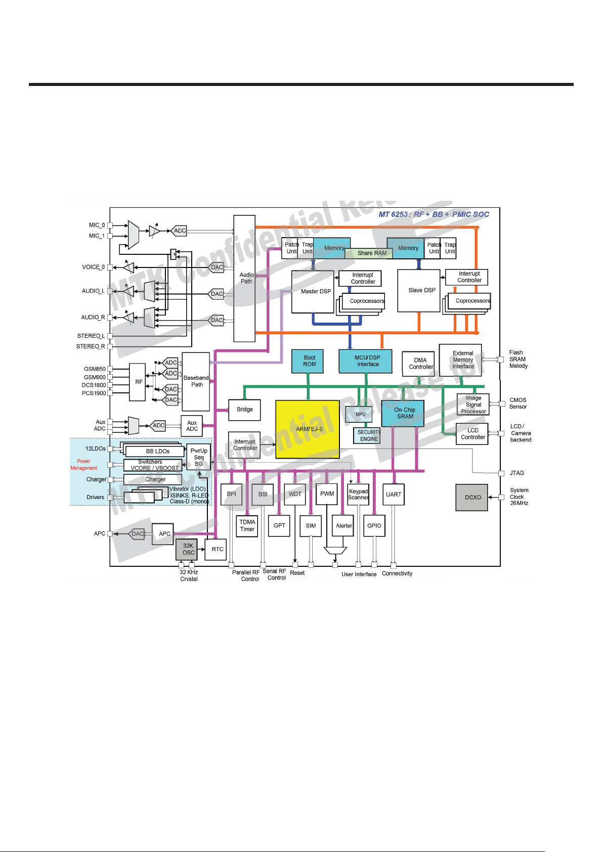
3.1 Digital Main Processor
Figure. 3.1.1 MT6253 Hardware Block Diagram

3.1.1 General
• Integrated voice-band, audio-band and base-band analog front ends.
• Package:
– aQFN, 11.5x11.5x0.85 mm.
– 0.47 mm pitch.
– 260balls, 0.47mm pitch package.
3.1.2 MCU Subsystem
• ARM7EJ-S 32-bit RISC processor.
• High performance multi-layer AMBA bus.
• Operating frequency 52/104MHz.
• Dedicated DMA bus, 7DMA channels.
• 144KB 0n-chip SRAM.
• On-chip boot ROM for Factory Flash Programming.
• Watchdog timer for system crash recovery.
• 3 sets of General Purpose Timer.
• Circuit Switch Data coprocessor.
• Division coprocessor.
3. TECHNICAL BRIEF
3.1.3 External Memory Interface
• Supports up to 3 external devices.
• Supports 16-bit memory components with maximum size of up to 64M Bytes for each bank.
• Supports Flash and SRAM/PSRAM with Burst Mode.
• Support legacy industry standard parallel LCD Interface.
• Suppport multi-media companion chips with 8/16 bits data width.
• Configurable driving strength for memory interface.
3.1.4 User Interface
• 6-row x 7-column keypad control with hardware scanner.
• Support multi key press for gaming.
• SIM/USIM Controller with hardware T=0/T=1 protocol control.
• Real Time Clock(RTC) operating with a separate power supply.
• General Purpose I/Os (GPIOs).
• 1 set of Pulse Width Modulation(PWM) Output.
• Alerter Output with Enhanced PWM or PDM.
• Maximum 7 external interrupt lines.
3.1.5 Security
Support security key and 128bit chip unique ID.
•
LGE Internal Use Only Copyright © 2012 LG Electronics. Inc. All right reserved.
- 15 -
Only for training and service purposes

- 16 -
LGE Internal Use Only Copyright © 2012 LG Electronics. Inc. All right reserved.
Only for training and service purposes
3. TECHNICAL BRIEF
3.1.6 Connectivity
• 3 sets of UART with hardware flow control and speed up to 921600 bps.
• IrDA modulator/demodulator with hardware framer supports SIR mode of operation.
• HS/FS/LS USB 2.0 Device controller.
• Multi Media Card/Secure Digital Memory Card/Memory Stick/Memory Stick Prto/SDIO host controller.
• Supports SDIO interface for SDIO peripherals as well as WIFI connectivity.
• DAI/PCM and !2S interface for Audio application.
3.1.7 Low Power Schemes
• Power Down Mode for analog and digital circuits.
• Processor Sleep Mode.
• Pause Mode of 32KHs clocking at Standby State.
• 3-channel Auxiliary 10-bit A/D Converter for application usage other than battery monitoring.
3.1.8 Power and Supply Management
• 2.8V to 4.7V Input Range.
• Charger Input up to 8V.
• 11 sets of LDO Optimized Specific GSM Sub-systems.
• One LDO for RF transceiver.
• High Operation Efficiency and Low Stand-by Current.
• Dual SIM Card Interface.
• One boost regulator and Four Open-Drain Output Current Regulators to Supply/Control the LED.
• LDO type Vibrator.
• One NMOS switch to control R(GB) LED.
• Thermal Overload Protection.
• Under Voltage Lock-out Protection.
• Over Voltage Protection.
3.1.9 Integrated RF Receiver
• Direct conversion architecture.
• Quad band differential input LNAs.
• Quadrature RF mixers.
• Fully integrated channel filter with f3dB=150kHs.
• 95dB gain with 60dB gain control range.
• No IIP2 calibration.

3.1.10 Integrated RF Transmitter
• Offset phase lock loop.
• IQ modulator DC offset calibration by BB ADC/DAC.
• Precise quadrature by IF divide-by-4.
• Integrated loop filter.
3.1.11 Integrated RF Frequency Synthesizer
• Programmable fractional-N synthesizer.
• Integrated wide range RFVCO.
• Integrated loop filter.
• Fast setting time suitable for multi-slot SPRS applications.
3.1.12 Integrated RF Digitally-Controlled Crystal Oscillator(DCXO)
• One-pin 26MHz crystal oscillator.
• On-chip programmable capacitor array for cross tune.
3. TECHNICAL BRIEF
3.1.13 Radio Interface and Baseband Front End
• GMSK modulator with analog I and Q channel outputs.
• 10-bit D/A Converter for uplink baseband I and Q signals.
• 14-bit high resolution A/D Converter for downlink baseband I and Q signals.
• Calibration mechanism of offset and gain mismatch for baseband A/D Converter and D/A
Converter.
• 10-bit D/A Converter for Automatic Power Control.
• Programmable Radio RX filter with adaptive bandwidth control.
• Dedicated Rx filter for FB acquisition.
• 6-Pin Baseband Parallel Interface(BRI) with programmable driving strength.
• Multi-band support.
3.1.14 Voice and Modem CODEC
• Digital tone generation.
• Voice Memo.
• Noise Reduction.
• Echo Suppression.
• Advanced Sidetone Oscillation Reduction.
• Digital sidetone generator with programmable gain.
• Two programmable acoustic compensation filters.
• GSM/GPRS quad vocoders for adaptive multirate(AMR), enhanced full rate(EFR), full.
rate(FR), and half rate(HR).
• GSM channel coding, equalization and A5/1, A5/2 and A5/3 ciphering.
• GPRS GEA1, GEA2 and GEA3 ciphering.
LGE Internal Use Only Copyright © 2012 LG Electronics. Inc. All right reserved.
- 17 -
Only for training and service purposes

- 18 -
LGE Internal Use Only Copyright © 2012 LG Electronics. Inc. All right reserved.
Only for training and service purposes
3. TECHNICAL BRIEF
3.1.15 Voice Interface and Voice Front End
• Two microphone inputs sharing one low noise amplifier with programmable gain and automatic gain control(AGC)
mechanism.
• Voice power amplifier with programmable gain.
• 2nd order Sigma-delta A/D Converter for voice uplink path.
• D/A Converter for voice downlink path.
• Supporter for voice downlink path.
• Supports half-duplex hands-free operation.
• Compliant with GSM 03.05
3.1.16 LCD Interface
• Dedicated Parallel Interface supports 2 external 8/9 bit Parallel Interface, and Serial interface for LCM.
3.1.17 LCD Controller
• Supports LCM format: RGB332, RGB444, RGB565, RGB666, RGB888.
• Supports LCD module with maximum resolution up to 240x320 at 16bpp.
• Capable of combining display memories with up to 4 blending layers.
• Accelerated Gamma correction with programmable gamma table.
• Supports hardware display rotation for each layer.
3.1.18 Audio CODEC
• Wavetable synthesis with up to 64 tones.
• Advanced wavetable synthesizer capable of generating and 47 sets of percussions.
• PCM Playback and Record.
• Digital Audio Playback.
3.1.19 Audio Interface and Audio Front End
• Supports I2S interface.
• High resolution D/A Converters for Stereo Audio playback.
• Stereo analog input for stereo audio source.
• Analog multiplexer for Stereo Audio.
• FM Radio Recording.
• Stereo to Mono Conversion.
• HE-AAC decode support.
3. TECHNICAL BRIEF
3.2 Power Management
Power management unit, so called PMU, is integrated into analog part. To facilitate software control and interface design,
PMU control share the CCI interface along with other analog parts, such as BBTX, BBRX, VBI and ABI during FT.
MT6253 PMU System
Charger
System
KPLED
Driver
LDOS
Buck
SIM IO 1 Boost
SIM IO 2
Power-on
Vibrator
Driver
Backlight
Driver
Sequence /
Protection
Speaker
Logic
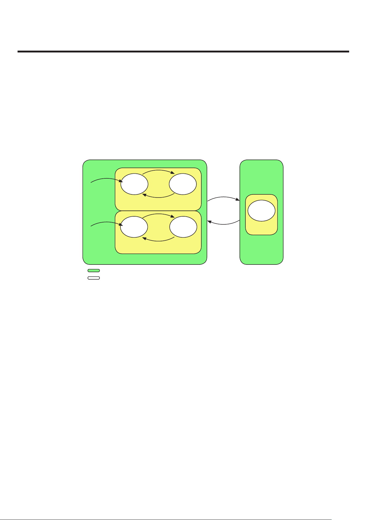
Figure. 3.2.1 PMU system block diagram
Driver
3.2.1 Low Dropout Regulators(LDOs), Buck converterand Reference
The PMU Integrates 12 LDOs that are optimized for their given functions by balancing quiescent current, dropout
voltage, line/load regulation, and output noise.
RF LDO (Vrf)
The RF LDO is a linear regulator that could source 180mA (max) with 2.8V output voltage. It supplies the RF circuitry of
the handset. The LDO is optimized for high performance and adequate quiescent current.
LGE Internal Use Only Copyright © 2012 LG Electronics. Inc. All right reserved.
- 19 -
Only for training and service purposes

- 20 -
LGE Internal Use Only Copyright © 2012 LG Electronics. Inc. All right reserved.
Only for training and service purposes
3. TECHNICAL BRIEF
Digital Core Buck Converter (Vcore)
The digital core regulator is a DC-DC step-down (Buck converter) that could source 200mA(max) with 1.2V to 0.9V
programmable output voltage based on software register setting. It supplies the power for baseband circuitry of the SoC.
The buck converter is optimized for high efficiency and low quiescent current.
Digital IO LDO (Vio)
The digital IO LDO is a linear regulator that could source 100mA (max) with 2.8V output voltage. It supplies the the
power for baseband circuitry of the SoC. The LDO is optimized for very low quiescent current and turns on automatically
together with Vm/Va LDOs.
Analog LDO (Va)
The analog LDO is a linear regulator that could source 100mA (max) with 2.8V output voltage.
It supplies the analog sections of the SoC. The LDO is optimized for low frequency ripple rejection in order to reject the
ripple coming from the burst at 217Hz of RF power amplifier.
TCXO LDO (Vtcxo)
The TCXO LDO is a linear regulator that could source 20mA (max) with 2.8V output voltage.
It supplies the temperature compensated crystal oscillator, which needs ultra low noise supply
with very good ripple rejection.
Single-Step RTC LDO (Vrtc)
The single-step RTC LDO is a linear regulator that can charge up a capacitor-type backup coin cell to 2.8V, which also
supplies the RTC module even at the absence of the main battery. The single-step LDO features the reverse current
protection and is optimized for ultra low quiescent current while sustaining the RTC function as long as possible.
Memory LDO (Vm)
The memory LDO is a linear regulator that could source 200mA (max) with 1.8V or 2.8V output voltage selection based on
the supply specification of memory chips. It supplies the memory circuitry in the handset. The LDO is optimized for very
low quiescent current with wide output loading range.
SIM LDO (Vsim)
The SIM LDO is a linear regulator that could source 80mA (max) with 1.8V or 3.0V output voltage selection based on
the supply specs of subscriber identity modules (SIM) card. It supplies the SIM card and SIM level shifter circuitry in the
handset. The Vsim LDO is controlled independently by the register named VSIM_EN.

3. TECHNICAL BRIEF
SIM2 LDO (Vsim2)
The SIM2 LDO is a linear regulator that could source 20mA (max) with 1.8V or 3.0V output voltage selection based on the
supply specs of the 2nd subscriber identity modules (SIM) card.
It supplies the 2nd SIM card and SIM level shifter circuitry in the handset. The Vsim2 LDO is controlled independently by
the register named VSIM2_EN.
USB LDO (Vusb)
The USB LDO is a linear regulator that could source 75mA (max) with 3.3V output dedicated for USB circuitry. It is
controlled independently by the register named RG_VUSB_EN.
Memory Card / Bluetooth LDO (Vbt)
The VBT LDO is a linear regulator that could source 150mA (max) with 1.5V, 1.8V, 2.5V or 2.8V output for memory card or
Bluetooth module. It is controlled independently by the register named RG_VBT_EN.
Camera Analog LDO (Vcama)
The Vcama LDO is a linear regulator that could source 150mA (max) with 1.5V, 1.8V, 2.5V or 2.8V output which is selected
by the register named VCAMA_SEL[1:0]. It supplies the analog power of the camera module. Vcama is controlled
independently by the register named RG_VCAMA_EN.
Camera Digital LDO (Vcamd)
The Vcamd LDO is a linear regulator that could source 75mA (max) with 1.3V, 1.5V, 1.8V or 2.8V output which is selected
by the register named VCAMD_SEL[1:0]. It supplies the digital power of the camera module. Vcamd is controlled
independently by the register named RG_VCAMD_EN.
LGE Internal Use Only Copyright © 2012 LG Electronics. Inc. All right reserved.
- 21 -
Only for training and service purposes
- 22 -
LGE Internal Use Only Copyright © 2012 LG Electronics. Inc. All right reserved.
Only for training and service purposes
3. TECHNICAL BRIEF
VCORE 1V2 / 1V0 200 mA PMU (BB)
VIO 2V8 100 mA
VRF 2V8 200 mA PAM
VA 2V8 125 mA BB(PLL, RFE, MBUF, AFE, RFD)
VM 1V8 / 2V8 200 mA EMI (BB), MEMORY
VTCXO 2V8 20 mA DCXO (BB)
VSIM 1V8 / 3V0 80 mA SIM1
VSIM2 1V8 / 3V0 20 mA SIM2, SIM3
VUSB 3V3 100 mA USB Power (BB)
VBT(VMMC) 1V8 / 2V84 / 3V0 150 mA MSDC (BB), T-FLASH
VCAM_A 1V5 / 1V8 / 2V5 / 2V8 150 mA CAMERA (ANALOG, IO)
VCAM_D 1V5 / 1V8 / 2V5 / 2V8 75 mA CAMERA (DIGITAL)
VRTC 2V8 1 mA
PULL UP(I2C1, I2C2, BT_PCMSYNC, BAT CONNECTOR)
SIM Selection, Jack DET, Hook DET, LCD, FM Radio
Table3.2.1. Power Supply Domains (Without RF)
3. TECHNICAL BRIEF
3.2.1 Power On
Together with Power Management IC (PMIC), MT6253 offers both fine and coarse resolutions of power control through
software programming. With this efficient method, the developer can turn on selective resources accordingly in order to
achieve optimized power consumption. The operating modes of MT6253 as well as main power states provided by the
PMIC are shown in Figure.3.2.1.
Power On
Power On
Active State
Active
Mode
Core
Processors
Power
Down Mode
Core
Processors
Software
Program
Software
Program
Sleep
Mode
Active
Mode
Software
Program
Pause
Mode
Core
Standby State
Phone Power State
Core Operating Mode
Figure 3.2.1. Major Phone Power States and Operating Modes for MT6253 based terminal
LGE Internal Use Only Copyright © 2012 LG Electronics. Inc. All right reserved.
- 23 -
Only for training and service purposes

- 24 -
LGE Internal Use Only Copyright © 2012 LG Electronics. Inc. All right reserved.
Only for training and service purposes
3. TECHNICAL BRIEF
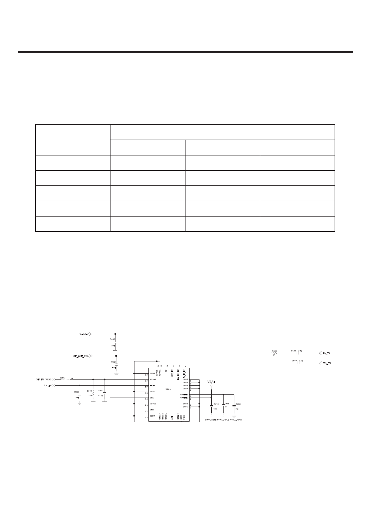
3.3 FEM with integrated Power Amplifier Module (SKY77550, U400)
3.3.1 Internal Block Diagram
SKY77550
TX_HB_IN(10)
VBATT (3)
VBATT (4)
HBT POWER AMPLIFIER
Match
(21) RX2
VRAMP (16)
TxEN (18)
BS (12)
VSW_EN (11)
Tx_LB_IN (9)
CURRENT SENSE
POWER AMPLIFIER CONTROL
LOGIC DECODER
(26) ANT
(19) RX1
Match
201287_001
Figure. 3.3.1 SKY77550 FUNCTIONAL BLOCK DIAGRAM
3.3.2 General Description
SKY77550 is a transmit and receive Front-End Module (FEM) with Integrated Power Amplifier Control(iPAC™) for Dualband cellular handsets comprising GSM850/900 and DCS1800/PCS1900 operation. Designed in a low profile, compact
form factor, the SKY77550 offers a complete Transmit VCO-to-Antenna and Antenna-to-Receive SAW filter solution. The
FEM also supports Class 12 General Packet Radio Service (GPRS) multi-slot operation.
The module consists of a GSM850/900 PA block and a DCS1800/PCS1900 PA block, impedance matching circuitry for
50 ohm input and output impedances, Tx harmonics filtering, high linearity / low insertion loss RF switch, and a Power
Amplifier Control (PAC) block with internal current sense resistor. The two Hetero-junction Bipolar Transistor (HBT) PA
blocks, a Bi-FET PAC and switch control circuit are fabricated onto a single Gallium Arsenide (GaAs) die. One PA block
supports the GSM850/900 bands and the other PA block supports the DCS1800/PCS1900 bands.
3. TECHNICAL BRIEF
C406
DNI
C400
DNI
C402
DNI
C409
56p
C408
1u
R402
51
C403 33p
C407
220p
33pC401
24K
R409
VBAT
10K
R407
U400
15
16
17
18
19
20
21
22
8
7
6
5
4
3
2
1
14
131211109
Tx_LB_IN
Tx_HB_IN
VSW_EN
BS
RSVD1
RSVD2
GND1
GND2
VBATT1
VBATT2
GND3
GND4
GND5
GND6
GND7
Rx2
RSVD3
Rx1
RSVD
TxEN
VRAMP
GND8
GND9
GND10
ANT
GND11
GND12
GND13
PGND
C410
10u
PA_EN
RF_ANT_SW1
RF_TX_RAMP
LB_TX
HB_TX
VLOGIC
(50V,C,NP0)(10V,2125) (50V,C,NPO)
Both PA blocks share common power supply pads to distribute current. The output of each PA block and the outputs
to the two receive pads are connected to the antenna pad through an RF switch. The GaAs die, Switch die and passive
components are mounted on a multi-layer laminate substrate. The assembly is encapsulated with plastic over mold.
Input Contrpol Bits
Mode
VSW_EN Tx_EN BS
STANDBY 0 0 0
1
Rx1
1
Rx2
Tx_LB 1 1 0
1 0 0
1 0 1
Tx_HB 1 1 1
1
Rx1 and Rx2 are broadband receive ports and each supports the GSM850, GSM900, DCS, and PCS nands.
Table 3.3.1 SKY77550 Mode Control Logic
LGE Internal Use Only Copyright © 2012 LG Electronics. Inc. All right reserved.
Figure 3.3.2 TX-module CIRCUIT DIAGRAM
- 25 -
Only for training and service purposes
- 26 -
LGE Internal Use Only Copyright © 2012 LG Electronics. Inc. All right reserved.
Only for training and service purposes
3. TECHNICAL BRIEF
C109 4.7u
X100
TSX-3225 26MHZ_7_4PF
26MHz
2 1
3 4
T4
V4
L33
K34
Y6
H6
M32
J31
RFVCO_MT
FREF
AU_VCM
PWM
XTAL1
XTAL2_GND
AVDD_RTC
BT_CLK_26M
3.4 Clocks
There are two major time bases in the MT6253. For the faster one is the 26 MHz clock originated from the digital control
oscillator(DCXO) of RF block. This is then converted to the square-wave signal through CLKSQ.
The other time base is the 32768 Hz clock generated by an on-chip oscillator connected to an external crystal.
26MHz
32KHz
DCXO
CLKSQ
1/2
MPLL
UPLL
XOSC_ANA
CLKSQ_26M_CK
CLKSQ_CON (0x8300_0100)
MPLI_113M_CK
PLL_CON0(0x8300_0200)
PLL_CON1(0x8300_0204)
MPLL_CON0(0x8300_0210)
MPLL_CON1(0x8300_0214)
UPLL_CON0(0x8300_0208)
UPLL_CON1(0x8300_020C)
UPLL_104M_CK
UPLL_48M_USB_CK
UPLL_48M_IRDA_CK
XOSCOUT
XOSC_CON(0x8300_0000)
1/2
USB PHY
CLKSQ_DIV2_MCU_SEL
(0x8300_0100[0])
1
0
CLKSQ_DIV2_MCU_SEL
(0x8300_0100[1])
1
0
CLKSQ_DIV2_GSM_SEL
(0x8300_0100[2])
1
0
CLKSQ_DIV2_USB_SEL
(0x8300_0100[3])
1
0
USB_PHY_CLK
MPLL_SEL
(0x8300_0204[1:0])
0
2
3
DPLL_SEL
(0x8300_0204[3:2])
0
2
3
GPLL_SEL
(0x8300_0204[4])
1
0
UPLL_SEL
(0x8300_0204[5])
1
0
FMCU_CK
FDSP_CK
FGSM_CK
FUSB_CK
F48M_CK
F32K_CK
MCU_DCM
EN
CG
DSP_DCM
EN
CG
GSM_DCM
EN
CG
USB_DCM
MSDC_DCM
EN
CG
EN
CG
SLOW_DCM
EN
CG
104MHz EMI_clock
104MHz AHB_clock
52MHz AHB_clock
52MHz APB_clock
104MHz GDSP1_CK
104MHz GDSP2_CK
52MHz GGSM_CK
52MHz BFE_clock
GUSB_CK
MSDC clock
IrDA clock
SLOW_CK
Figure. 3.4.1 Clock distributions inside the MT6253.
Figure. 3.4.2 Crystal Oscillator External Connection

3. TECHNICAL BRIEF
3.4.1 32.768KHz Time Base
The 32768 Hz clock is always running. It’s mainly used as the time base of the Real Time Clock(RTC) module, which
maintains time and date with counters. Therefore, both the 32768Hz oscillator and the RTC module is powered by
separate voltage supplies that shall not be powered down when the other supplies do.
In low power mode, the 13Mhz time base is turned off, so the 32768Hz clock shall be employed to update the critical
TDMA timer and Watchdog Timer. This time base is also used to clocks the keypad scanner logic
3.4.2 26MHz Time Base
Since PLL are based on 13MHz reference clock. There is an ½-dividers for PLL existing to allow using 26MHz DCXO.
There are 2 phase-locked loops(PLL) in MT6253. The UPLL generates 624Mhz clock output, then a frequency divider
further divide 6, and 13 to generate fixed 103Mhz, and 48Mhz for GSM_CLOCK and USB_CLOCK and DSP_CLOCK. These
four primary clocks then feed into GSM, USB, MCU and DSP Clock Domain, respectively.
These 2 PLLs require no off-chip components for operations and can be turn off in order to save power. After power-on,
the PLLs are off by default and the source clock signal is selected through multiplexers. The software shall take cares of
the PLL lock time while changing the clock selections. The PLL and usages are listed below.
- PLL supply four clock source : MCU_CLOCK(104~113Mhz), DSP_CLOCK(104~113Mhz),
GSM_CLOCK(104Mhz) and USB_CLOCK(48Mhz)
- For DSP/MCU system clock, MCU_CLOCK and DSP_CLOCK. The outputted 104~113Mhz clock is controlled by MCU for
500Khz per step and settled time is under 100uS. The clock is also connected to DSP/MCU DCM (dynamic clock manager)
for dynamically adjusting clock rate by digital clock divider.
MCU_CLOCK paces the operations of the MCU cores, MCU memory system, and MCU peripherals as well
Modem system clock, GSM_CLOCK, which paces the operations of the GSM/GPRS hardware, coprocessors as well. The
outputted 104Mhz clock is connecter to GSM_DCM for dynamically adjusting clock rate by digital clock divider. Typically
the GSM_DCM output clock no more than 52Mhz.
Note that PLL need some time to become stable after being powered up. The software shall take cares of the PLL lock
time before switching them to the proper frequency. Usually, a software loop longer than the PLL lock time is employed
to deal with the problem.
For power management, the MCU software program may stop MCU Clock by setting the Sleep Control Register. Any
interrupt requests to MCU can pause the sleep mode, and thus MCU return to the running mode.
AHB also can be stop by setting the Sleep Control Register. However the behavior of AHB in sleep mode is a little different
from that of MCU. After entering Sleep Mode, it can be temporarily waken up by any “hreq”(bus request), and then goes
back to sloop automatically after all “hreqs” de-assert. Any transactions can take place as usual in sleep mode, and it can
save power while there is no transaction on it. However the penalty is losing a little system efficiency for switching on
and off bus clock, but the impact is small
LGE Internal Use Only Copyright © 2012 LG Electronics. Inc. All right reserved.
- 27 -
Only for training and service purposes
- 28 -
LGE Internal Use Only Copyright © 2012 LG Electronics. Inc. All right reserved.
Only for training and service purposes
3. TECHNICAL BRIEF
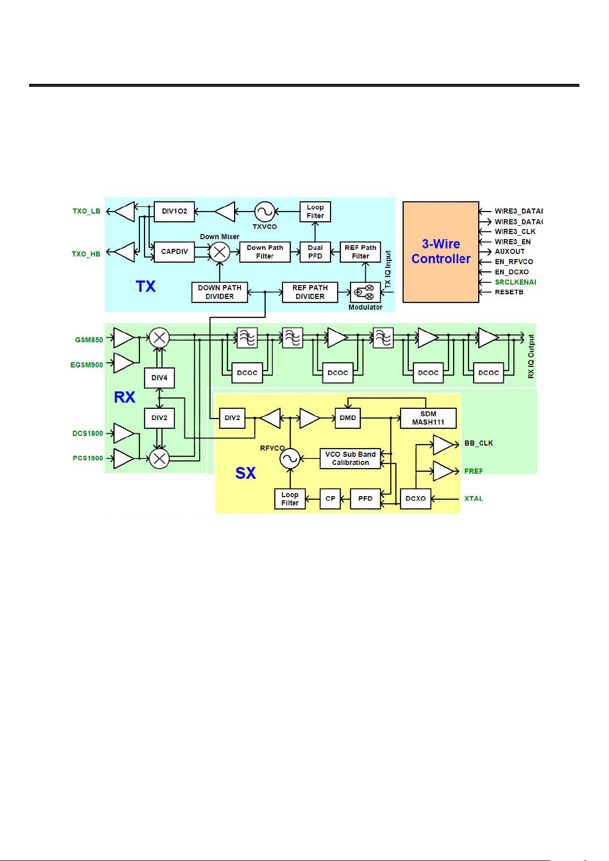
3.5 RFSYS of MT6253 (U101)
Figure. 3.5.1 Block DIAGRAM of RFSYS
3.5.1 GENERAL DESCRIPTION
RFSYS built in MT6253 SOC is a highly integrated RF transceiver for multi-band GMS and GPRS cellular systems. The
features are listed as following.
Receiver
- Direct conversion architecture
- Quad band differential input LNAs
- Quadrature RF mixers
- Fully integrated channel filter with f
- 95 dB gain with 60 dB gain control range
=150kHz
3dB

Transmitter
- Offset phase lock loop.
- IQ modulator.
- Integrated TX VCO.
- Integrated loop filter.
Frequency Synthesizer
- Programmable fractional-N synthesizer.
- Integrated wide range RFVCO.
- Integrated loop filter.
- Fast settling time suitable for multi-slot GPRS/EDGE applications.
Digitally-Controlled Crystal Oscillator (DCXO)
- One-pin 26 MHz crystal oscillator.
- On-chip programmable capacitor array for coarse tune.
- On-chip programmable capacitor array for fine tune.
3. TECHNICAL BRIEF
RFSYS in a-QFN package
LGE Internal Use Only Copyright © 2012 LG Electronics. Inc. All right reserved.
- 29 -
Only for training and service purposes
- 30 -
LGE Internal Use Only Copyright © 2012 LG Electronics. Inc. All right reserved.
Only for training and service purposes
3. TECHNICAL BRIEF
M18 AD Mux Family with Synchronous PSRAM
PSRAM Die
(Non-Multiplex I/O)
Flash Die
(Address/Data Multiplex I/O)
VSS
A[MAX:16]
DQ[15:0]
CLK
F-WP#
ADV#
F-WE#
VCCQ
WAIT
A[MAX:0]
A/DQ[15:0]
F1-CE#
F1-OE#
F1-VCC
F-VPP
F-RST#
P-CS#
R-OE#
P-CRE
R-WE#
R-LB#
R-UB#
P-VCC
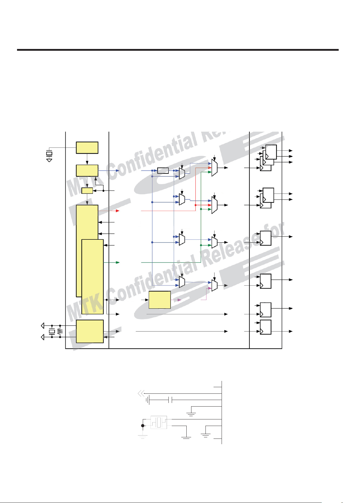
3.6 MEMORY(PF38F5060M0Y3DK, U100 )
3.6.1 Functional Description
The Numonyx™ StrataFlash® Cellular Memory (M18) device provides high read and write performance at low voltage on a
16-bit data bus.
The flash memory device has a multi-partition architecture with read-while-program and read-while-erase capability.
The device supports synchronous burst reads up to 108 MHz using ADV# and CLK address-latching (legacy-latching)
on some litho/density combinations and up to 133 MHz using CLK address-latching only on some litho/density
combinations. It is listed below in the following table.
Sync PSRAM AD-Mux I/O Block Diagram.
Notes:
1. F2-OE# must be treated as an RFU, Howerver, to ensure future compatibility, F2-OE# can be tied to F1-OE# or left
floated.
2. F2-VCC must be treated as an RFU, Howerver, to ensure future compatibility, F2-VCC can be tied to F1-VCC or left
floated.
3. For full AD-Mux (NOR/PSRAM), PSRAM Address[15:0] are shared with NOR ADQ[15:0]; See Figure, “ “ on apge 27.
4. For full AD-Mux (NOR/PSRAM) all address/data are shared with NOR ADQ[15:0], Upper addresses [Max:16] should be
connected to VSS.
Figure. 3.6.1 MEMORY BLOCK DIAGRAM
 Loading...