

LG A258 Service Manual

Internal Use Only
Service Manual
LG-A258
Date: June, 2011 / Issue 1.0

- 2 -
LGE Internal Use Only Copyright © 2011 LG Electronics. Inc. All right reserved.
Only for training and service purposes
Table Of Contents
1. INTRODUCTION ................................................................... 3
1.1 Purpose .....................................................................................................3
1.2 Regulatory Information ...................................................................... 3
1.3 Abbreviations..........................................................................................5
2. PERFORMANCE .................................................................... 7
2.1 H/W Features ...........................................................................................7
2.2 Technical Specification ........................................................................9
3. TECHNICAL BRIEF ..............................................................14
3.1 LG-A258 Functional Block Diagram ............................................ 14
3.2 Digital Main Processor (PMB8815, U200) ................................. 15
3.3 Power Management ......................................................................... 20
3.4 FEM with integrated Power Amplifier Module
(SKY77550, U301) ...............................................................................33
3.5 Crystal(26 MHz, X100) ...................................................................... 36
3.6 RF Subsystem of PMB8815 (U101) .............................................. 37
3.7 MEMORY ................................................................................................ 40
3.8 Bluetooth module .............................................................................. 45
3.9 SIM Card Interface .............................................................................. 47
3.10 LCD Interface .....................................................................................48
3.11 Vibrator Interface .............................................................................49
3.12 MINI ABB Interface .......................................................................... 50
3.13 Keypad Interface .............................................................................. 53
3.14 Audio Front-End ............................................................................... 55
3.15 Camera Interface .............................................................................. 61
3.16 KEY BACLKLIGHT LED Interface ................................................. 63
4. TROUBLE SHOOTING ........................................................64
4.1 Trouble shooting test setup ........................................................... 64
4.2 RF Component .................................................................................... 65
4.3 RX Trouble ............................................................................................. 66
4.4 TX Trouble .............................................................................................. 72
4.5 Power On Trouble ............................................................................... 78
4.6 Charging Trouble ................................................................................ 81
4.7 Vibrator Trouble .................................................................................. 84
4.8 LCD Trouble .......................................................................................... 87
4.9 Camera Trouble ................................................................................... 91
4.10 Speaker Trouble ................................................................................ 94
4.11 Earphone Trouble ............................................................................97
4.12 Micro SD Trouble
4.13 Bluetooth Trouble ..........................................................................104
4.14 FM Radio Trouble ...........................................................................106
5. DOWNLOAD .....................................................................109
6. BLOCK DIAGRAM .............................................................122
7. CIRCUIT DIAGRAM ..........................................................123
8. BGA PIN MAP ..................................................................128
9. PCB LAYOUT .....................................................................130
10. STAND ALONE TEST ......................................................132
10.1 Introduction .....................................................................................132
10.2 Setting Method ..............................................................................132
10.3 Tx Test .................................................................................................134
10.4 Rx Test .................................................................................................135
11.AUTO CALIBRATION .......................................................136
11.1 Overview ...........................................................................................136
11.2 Directory structure of Tachyon .................................................136
11.3 Description of Folder & File. .......................................................137
11.4 Procedure ..........................................................................................138
11.5 Tachyon Main UI .............................................................................139
11.6 AGC ......................................................................................................140
11.7 APC ......................................................................................................140
11.8 ADC ......................................................................................................140
11.9 Target Power ....................................................................................140
12. EXPLODED VIEW & REPLACEMENT PART LIST ..........141
12.1 EXPLODED VIEW .............................................................................141
12.2 Replacement Parts ........................................................................142
12.3 Accessory ..........................................................................................157
............................................................................102

1. INTRODUCTION
1.1 Purpose
This manual provides the information necessary to repair, calibration, description and download the features
of this model.
1.2 Regulatory Information
A. Security
Toll fraud, the unauthorized use of telecommunications system by an unauthorized part (for example, persons
other than your company’s employees, agents, subcontractors, or person working on your company’s behalf)
can result in substantial additional charges for your telecommunications services. System users are
responsible for the security of own system. There are may be risks of toll fraud associated with your
telecommunications system. System users are responsible for programming and configuring the equipment
to prevent unauthorized use. The manufacturer does not warrant that this product is immune from the above
case but will prevent unauthorized use of common-carrier telecommunication service of facilities accessed
through or connected to it.
The manufacturer will not be responsible for any charges that result from such unauthorized use.
B. Incidence of Harm
If a telephone company determines that the equipment provided to customer is faulty and possibly causing
harm or interruption in service to the telephone network, it should disconnect telephone service until repair
can be done. A telephone company may temporarily disconnect service as long as repair is not done.
C. Changes in Service
A local telephone company may make changes in its communications facilities or procedure. If these changes
could reasonably be expected to affect the use of the this phone or compatibility with the network, the
telephone company is required to give advanced written notice to the user, allowing the user to take
appropriate steps to maintain telephone service.
D. Maintenance Limitations
Maintenance limitations on this model must be performed only by the manufacturer or its authorized agent.
The user may not make any changes and/or repairs expect as specifically noted in this manual. Therefore, note
that unauthorized alternations or repair may affect the regulatory status of the system and may void any
remaining warranty.
1. INTRODUCTION
LGE Internal Use Only Copyright © 2011 LG Electronics. Inc. All right reserved.
- 3 -
Only for training and service purposes

- 4 -
LGE Internal Use Only Copyright © 2011 LG Electronics. Inc. All right reserved.
Only for training and service purposes
1. INTRODUCTION
E. Notice of Radiated Emissions
This model complies with rules regarding radiation and radio frequency emission as defined by local
regulatory agencies. In accordance with these agencies, you may be required to provide information such as
the following to the end user.
F. Pictures
The pictures in this manual are for illustrative purposes only; your actual hardware may look slightly different.
G. Interference and Attenuation
Phone may interfere with sensitive laboratory equipment, medical equipment, etc. Interference from
unsuppressed engines or electric motors may cause problems.
H. Electrostatic Sensitive Devices
ATTENTION
Boards, which contain Electrostatic Sensitive Device (ESD), are indicated
by the sign. Following information is ESD handling:
• Service personnel should ground themselves by using a wrist strap when exchange system boards.
• When repairs are made to a system board, they should spread the floor with anti-static mat which is also
grounded.
• Use a suitable, grounded soldering iron.
• Keep sensitive parts in these protective packages until these are used.
• When returning system boards or parts like EEPROM to the factory, use the protective package as described.
1.3 Abbreviations
For the purposes of this manual, following abbreviations apply:
Offset Phase Locked LoopOPLL
Light Emitting DiodeLED
Low Drop OutputLDO
Liquid Crystal DisplayLCD
Intermediate FrequencyIF
International Portable User IdentityIPUI
Global System for Mobile CommunicationsGSM
General Purpose Interface BusGPIB
Gaussian Minimum Shift KeyingGMSK
Flexible Printed Circuit BoardFPCB
Electrostatic DischargeESD
Electrical Erasable Programmable Read-Only MemoryEEPROM
Digital Signal ProcessingDSP
dB relative to 1 milli wattdBm
Digital Communication SystemDCS
Digital to Analog ConverterDAC
Constant Current – Constant VoltageCC-CV
Bit Error RatioBER
BasebandBB
Automatic Power ControlAPC
1. INTRODUCTION
LGE Internal Use Only Copyright © 2011 LG Electronics. Inc. All right reserved.
- 5 -
Only for training and service purposes
1. INTRODUCTION
Wireless Application Protocol
WAP
Voltage Control Temperature Compensated Crystal OscillatorVCTCXO
Voltage Controlled OscillatorVCO
Universal Asynchronous Receiver/TransmitterUART
Time Division Multiple AccessTDMA
Time Division DuplexTDD
Travel AdapterTA
Side Tone Masking RatingSTMR
Pseudo SRAMPSRAM
Static Random Access MemorySRAM
Sending Loudness RatingSLR
Subscriber Identity ModuleSIM
Surface Acoustic WaveSAW
Real Time ClockRTC
Root Mean SquareRMS
Receiving Loudness RatingRLR
Radio FrequencyRF
Public Switched Telephone NetworkPSTN
Phase Locked LoopPLL
Programmable Gain AmplifierPGA
Printed Circuit BoardPCB
Power Amplifier ModulePAM
LGE Internal Use Only Copyright © 2011 LG Electronics. Inc. All right reserved.
- 6 -
Only for training and service purposes
2. PERFORMANCE
2.1 H/W Features
Item Feature Comment
Standard Battery Lithium-ion r, 3.7V, 900mAh
Stand by TIME
Up to 290 hrs ( Paging Period 5, RSSI -85dBm )
Talk time Up to 361min : GSM Tx Level 7
Charging time Approx. 3 hours
TX output power
GSM, EGSM: 33dBm(Level 5),
DCS , PCS: 30dBm(Level 0)
SIM card type 3V Small
Display
MAIN : 2.2” TFT 176 Ý 220 pixel 262K Color
Sub : 0.968 mono 96 x 64
Status Indicator
Button (Outside)
Send Key, End Key, Navi Key(4EA), OK Key, Menu Key,
Contacts Key
Button (Inside)
Numeric Key 12EA
ANT Internal
EAR Phone Jack 5PIN I/O
PC Synchronization Yes
Speech coding
EFR/FR/HR/AMR
Data and Fax Yes
GPRS compatibility Class 12
Vibrator Yes
Loud Speaker Yes
Voice Recoding Yes
Microphone Yes
RX Sensitivity
GSM, EGSM: -109dBm, DCS: -109dBm
2. PERFORMANCE
LGE Internal Use Only Copyright © 2011 LG Electronics. Inc. All right reserved.
- 7 -
Only for training and service purposes
- 8 -
LGE Internal Use Only Copyright © 2011 LG Electronics. Inc. All right reserved.
Only for training and service purposes
2. PERFORMANCE
Travel Adapter Yes
Speaker/Receiver 18x12Ȱ Speaker/ Receiver
MIDI SW MIDI (Mono SPK)
Item Feature Comment
Camera 1.3M
Bluetooth / FM Radio Bluetooth version 2.1 / 76~108MHz supported
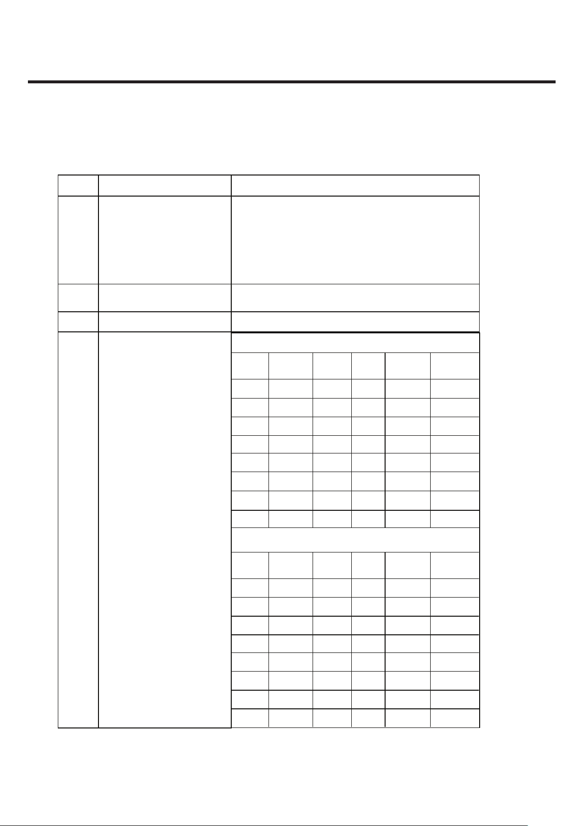
2.2 Technical Specification
Item Description Specification
1 Frequency Band
EGSM
TX: 880 ~ 915MHz
RX: 925 ~ 960 MHz
DCS
TX: 1710 ~ 1785 MHz
RX: 1805 ~ 1880 MHz
2 Phase Error
RMS < 5 degrees
Peak < 20 degrees
3 Frequency Error < 0.1 ppm
4 Power Level
Level Power Toler. Level Power Toler.
6 31dBm ·3dB 14 15dBm · 3dB
7 29dBm ·3dB 15 13dBm · 3dB
8 27dBm ·3dB 16 11dBm · 5dB
9 25dBm ·3dB 17 9dBm · 5dB
10 23dBm ·3dB 18 7dBm · 5dB
11 21dBm ·3dB 19 5dBm · 5dB
12 19dBm ·3dB
GSM850 / EGSM
5 33dBm ·2dB 13 17dBm · 3dB
Level Power Toler. Level Power Toler.
1 28dBm ·3dB 9 12dBm · 4dB
2 26dBm ·3dB 10 10dBm · 4dB
3 24dBm ·3dB 11 8dBm · 4dB
4 22dBm ·3dB 12 6dBm · 4dB
5 20dBm ·3dB 13 4dBm · 4dB
6 18dBm ·3dB 14 2dBm · 5dB
7 16dBm ·3dB 15 0dBm · 5dB
DCS/PCS
0 30dBm ·2dB 8 14dBm · 3dB
GSM850
TX: 824 ~ 849 MHz
RX: 869 ~ 894 MHz
PCS
TX: 1850 ~ 1910 MHz
RX: 1930 ~ 1990 MHz
2. PERFORMANCE
LGE Internal Use Only Copyright © 2011 LG Electronics. Inc. All right reserved.
- 9 -
Only for training and service purposes
- 10 -
LGE Internal Use Only Copyright © 2011 LG Electronics. Inc. All right reserved.
Only for training and service purposes
2. PERFORMANCE
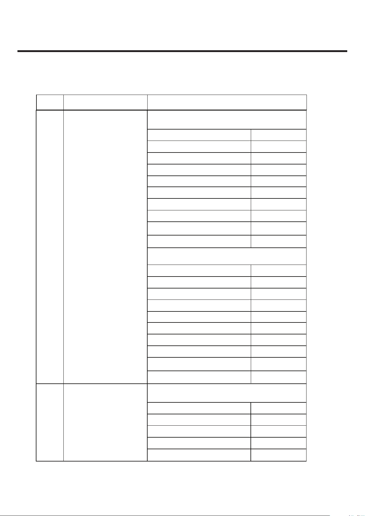
5
Output RF Spectrum
(due to modulation)
Offset from Carrier (kHz). Max. dBc
100 +0.5
200 -30
250 -33
400 -60
600~ <1,200 -60
1,200~ <1,800 -60
1,800~ <3,000 -63
3,000~ <6,000 -65
6,000 -71
GSM850/EGSM
Offset from Carrier (kHz). Max. dBc
100 +0.5
200 -30
250 -33
400 -60
600~ <1,200 -60
1,200~ <1,800 -60
1,800~ <3,000 -65
3,000~ <6,000 -65
6,000 -73
DCS/PCS
6
Output RF Spectrum
(due to switching
transient)
GSM850/EGSM
Offset from Carrier (kHz). Max. dBm
400 -19
600 -21
1,200 -21
1,800 -24
Item Description Specification
Item Description Specification
6
Output RF Spectrum
(due to switching
transient)
Offset from Carrier (kHz). Max. dBm
400 -22
600 -24
1,200 -24
1,800 -27
7 Spurious Emissions Conduction, Emission Status
8 Bit Error Ratio
GSM850, EGSM
BER (Class II) < 2.439% @-102 dBm
DCS, PCS
BER (Class II) < 2.439% @-102 dBm
9 RX Level Report Accuracy ·3 dB
10 SLR 14·3 dB
11 Sending Response
300 -12
1,000 -6
2,000 -6
3,000 -6
Frequency (Hz) Max.(dB) Min.(dB)
100 -
200 -
4,000 -
3,400 -9
0
0
4
4
-12
0
0
4
12 RLR 4·3 dB
DCS/PCS
2. PERFORMANCE
LGE Internal Use Only Copyright © 2011 LG Electronics. Inc. All right reserved.
- 11 -
Only for training and service purposes
- 12 -
LGE Internal Use Only Copyright © 2011 LG Electronics. Inc. All right reserved.
Only for training and service purposes
2. PERFORMANCE
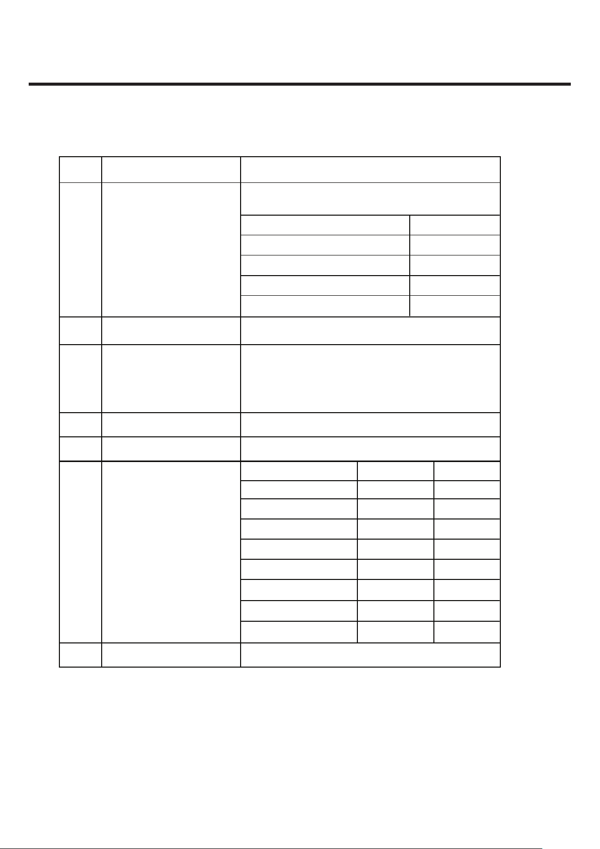
Item Description Specification
13 Receiving Response
300 -7
500 -5
1,000 -5
3,000 -5
Frequency (Hz) Max.(dB) Min.(dB)
100 -
200 -
4,000
3,400 -10
2
*
0
2
-12
0
2
2
14 STMR Over 17 dB
* Mean that Adopt a straight line in between 300 Hz
and 1,000 Hz to be Max. level in the range.
15 Stability Margin > 6 dB
-20
-10
0
7
dB to ARL (dB) Level Ratio (dB)
-35
-30
10
30.7
33.3
33.7
31.7
17.5
22.5
25.5
16 Distortion
17 Side Tone Distortion Three stage distortion < 10%
18
System frequency
(26 MHz) tolerance
˺ 2.5 ppm
19 32.768KHz tolerance ˺ 30 ppm
20 Ringer Volume
At least 58 dB SPL under below conditions:
1. Ringer set as ringer.
2. Test distance set as 100 cm
Item Description Specification
21 Charge Current
Fast Charge : Typ. 400 mA
Slow Charge : Typ. 400mA
Total Charging Time : < 3 hours
2 -> 1
0 -> OFF
Bar Number Power
4 -> 2
-104 · 2
-106 Under
-98 · 2
-101 · 2
22 Antenna Display
23 Battery Indicator
24
Low Voltage Warning
( Blinking Bar)
25
Forced shut down
Voltage
3.35 · 0.05V
27 Battery Type
Lithium-Ion Battery
Standard Voltage = 3.7 V
Battery full charge voltage = 4.2 V
Capacity: 900mAh
28 Travel Charger
Switching-mode charger
Input: 100 ~ 240V, 50/60 Hz
Output: 5.1V, 400 mA
26
Sustain RTC
without battery
Over 30 sec
7
7 -> 5
5 -> 4
-92 Over
-93 · 2
1 -> 0 -106 · 2
It alarms 3 times (standby)10% : 1
st
warning 5% : 2
nd
warning 0% : 3rdwarning
It alarms every 1min under 10%(call)
13 level(Full)
12
11
10
9
4
3
2 / 2
0
8
5
6
1
100~93%
92~85%
84~77%
76~70%
69~62%
61~54%
46~39%
30~24%
38~31%
23~16%
15~11% 10~8%
7 53~47%
7~1%
0%
/
2. PERFORMANCE
LGE Internal Use Only Copyright © 2011 LG Electronics. Inc. All right reserved.
- 13 -
Only for training and service purposes

- 14 -
LGE Internal Use Only Copyright © 2011 LG Electronics. Inc. All right reserved.
Only for training and service purposes
3. TECHNICAL BRIEF
3. TECHNICAL BRIEF
.(<3DG
6,0
9LEUDWRU
7)ODVK
X)&$3IRU57&
7;0RGXOH
*60
7[0RGXOH
ELW,&
6',2ELW
0&$0
7[/RZ+LJK
&75/6LJQDO
4Z')5/&%5
7)7/&'
Ě
4&,)
7)7/&'
Ě
4&,)
0/('
/&'B&75/
/&',)
ELW
,&
986%
75$16&(,9(5
*60
5[6$:
4Z2%5
+%B5;B13
/%B5;B13
1$1')ODVK
*ELW
1$1',)
;00
0(025<
86%
8$57
SLQ&RQQ
/*\A$6
0,1,$%%
,&,)
57*4:
08,&
&KDUJLQJ
/*\
''56'5$0
0ELW
%7
6'5$0,)
3&08$57
8$57
+HDGVHW
)0B$17
$*5
/(''ULYLQJ
/'2
8$577[5[
86%)6
-*\A$6
$XGLR
6XE6
\
VWHP
,&
63((&+
86%)6'3'0
+60LF,1
)05DGLR
+663((&+
+6030,',
\
73$3
,&,)
308
63.5&9
030,',/5
)05$',2/5
0LF,1
+6)05$',2
-*\
P$K/LLRQ
&KDUJLQJ
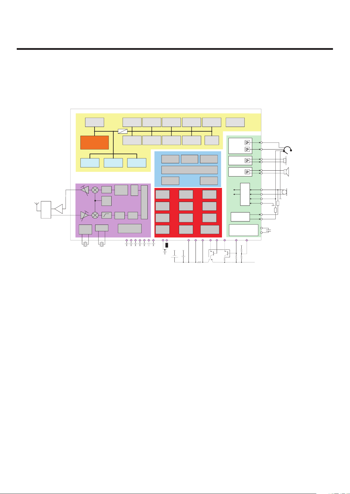
3.1 LG-A258 Functional Block Diagram
The functional component arrangement is mentioned below diagram.
Figure. 3.1.1 LG-A258 Functional Block Diagram
FM - radio
Digi tal -
Mic rophone
ARM11 76
RAM ROMcac he
Ext ernal
Mem ory- IF
USI F
Mea surem ent
IF (A/D)
SD/ MM C SIM
GSM
TEA KLite
RF
Co ntro l
GSM
Ci pher
GPT U
I² S / DA I
IR - M emor y
Loud spe aker
Mic Supply
gener ation
HSR
HSL
EPP
EPN
LSP
LSN
MI CP1
MI CN1
MI CP2
MI CN2
Mic
MU X
VM IC
VUM IC
16 O hm
100 m W
8 Ohm
700 m W
2x 16 Ohm
2x 30 mW
Ster eo
Hea dset
Earpie ce
Cha rge Pu mp
(n egativ e vo ltage for
bipola r audio out )
VMM C
VAN ALPM U
VUS B
LA UX
Ch arg e
DC/ D C
Bu ck
Vib rato r
64 - b it b us 32 - b it b us
IF
GMS K
DA C
SD
PLL
FEM
32 kH z
XO
DSPAD C
PA
c
s
iM
Lo wPow er
DC XO
RF PM U
USB 2.0
FS
CI F
DC C
Key pad
4k7
0. 15 5 %
1.8V ~2.5V
VCHARGE 4. 5 V … 20V
2
T
AB
V
N
ESNE
S
PES
N
ES
S
C
C
S
B
GHC
D
D
V
TN
H
SV
BC 847 S
1 2
6
4
5
3
for example
ZXT P 25020
min.
10 µF
(0 V ) 3.05 V … 5.1 V (6 V)
002
>ef
h
T 1
A
m5
.1
.x
a
m
7.5µA
135 mV … 600mV
GH
C
V
4k3
127k
470
1.0V…
1,8V
Vco re
LR TC
LSI M
Bac k -
lig ht
LDO bloc king c aps, 100 nF
DC/ DC
Batt ery Charge r
3.2 Digital Main Processor (PMB8815, U101)
3. TECHNICAL BRIEF
Figure. 3.2.1 X-Gold 215 Hardware Block Diagram
Only for training and service purposes
LGE Internal Use Only Copyright © 2011 LG Electronics. Inc. All right reserved.
- 15 -

- 16 -
LGE Internal Use Only Copyright © 2011 LG Electronics. Inc. All right reserved.
Only for training and service purposes
3. TECHNICAL BRIEF
3.2.1 General
Technology:
– SoC, Monolithic, 65 nm CMOS
• Package:
– eWLB, 8x9x0.8 mm
– 0.5 mm pitch
– 240 balls / 6-layer PCB
3.2.2 RF Transceiver
• Dual-band direct conversion receiver
• Tri/Quad-band possible with external circuitry
• Fully integrated digital controlled X0
• Additional buffer for 2 external system clocks
• Fully digital RF-Synthesizer incl. ȭȟ-Transmitter
3.2.3 Baseband
• DSP:
– 178 MHz TeakLite™
• MCU:
– ARM ® 1176 @ 208 MHz
• MCU RAM:
– 3.00Mbit
• Memory I/F:
– 1Gbit NOR flash/One NAND flash/SDR SDRAM
– 4Gbit NAND flash/DDR SDRAM
• Modem:
– GPRS class 12, (RX/TX CS1-CS4)
– EGPRS class 12, (RX MCS1-MCS9, TX MCS1-MCS4)
• Cipher Units:
– A51/2/3
– GEA-1/2/3
• Security:
– OMTP TR0
– Secure Boot
– RSA(ROM)/SHA-1(HW accel.)
– OCDS disabling
– Certificate Management

• Speech Codec:
– FR / HR / EFR / NB-AMR
• Audio Codec (running on ARM1176):
– SP-MIDI
– SB-ADPCM
– MP3
– WB-AMR
– AAC/AAC+/eAAC+
• Others:
– DARP (SAIC)
– TTY
• Customization:
– E-Fuses
3.2.4 External Memory
• External Bus Unit
– 16-bit address bus
– 16-bit address/data muxed bus
– 1.8V support
• Flash / RAM
– NOR Type
– NAND Type(1bit ECC supported)
– Parallel Flash/Cellular RAM(Page & Burst Mode)
- 16-bit AD-multiplexed(concurrent usage of DDR interface and AD-multiplexed interface is not supported)
- 16-bit AAD-multiplexed
– iNAND Type e.g. oneNAND
– SDRAM
- DDR SDRAM : up to 4 Gbit
- SDR SDRAM : up to 1 Gbit
• Memory card
– SD/MMC card interface with 1 or 4 data lines
3.2.5 Connectivity
• Up to 3xUSIF (configurable either as SPI or UART), I2C, I2S; Interfaces @ 1.8V
• Direct (U)SIM 1.8/3V
• USB2.0 up to 480 Mbit/s (High Speed) w/ external USB Phy over ULPI interface
• Stereo Headset (Amplifier integrated)
• 3 external analog measurement PIN’s
• Bluetooth, A-GPS, WLAN support (I2C, I2S, SPI)
3. TECHNICAL BRIEF
LGE Internal Use Only Copyright © 2011 LG Electronics. Inc. All right reserved.
- 17 -
Only for training and service purposes

- 18 -
LGE Internal Use Only Copyright © 2011 LG Electronics. Inc. All right reserved.
Only for training and service purposes
3. TECHNICAL BRIEF
3.2.6 Mixed Signal
• Improved audio performance
• Loudspeaker Audio Class D Amplifier, 700 mW@8 ȳ mono for hands-free and ringing
• Stereo Headset 2x30 mW@16 ȳ w/o coupling C
• Mono Earpiece 100 mW@16 ȳ
• Digital microphone supported
• Differential microphone input
3.2.7 FM Radio
• Integrated FM radio
– FM Stereo RDS Receiver
– Sensitivity 2 ɆV EMF
– Support for US & EU bands
– Stereo recording
3.2.8 Power Management
• Direct-to-Battery Connection
– LDOs (incl. capless)
– DC/DC step-down converter
– DC/DC step-up for white LED supply
• Battery Type
– Li-Ion
• Charging control
– Battery temperature
– Watchdog protection
– Start-up on flat battery
• External Charger
– Switch mode
• USB battery charging
– USB charging spec 1.0 compliant
• Backlight
– Up to 4 serial white LEDs (integrated LDO)

3. TECHNICAL BRIEF
3.2.9 Display
• Type
– 128x160, 65k color (serial)
– QVGA, 262k color (parallel)
• Interface
– Parallel 8/9bit MIPI-DBI Type B
– Serial MIPI-DBI Type C
– Interf. voltage at 1.8V or 2.8V
• gRacr - Display Controller (Hardware)
– 30 fps Display update without DMA (up to 60 fps) (full or partial)
– Video post processing Scaling, Rotation (90¶ steps), Mirroring
– Overlay with alpha blending
– Color conversion YUV -> RGB
– 2D vector graphics (Lines, filled rectangles, Bit block transfer (e.g. sprites, scrolling, antialiased bitmap fonts)
3.2.10 Camera
• 2 Mpx YUV parallel interface
• HW JPEG encoder (39 Mpx/sec)
• 39 MHz Pixel Rate
• 15 fps@ 2 Mpx full resolution
3.2.11 Video Capabilities
• Video Decoding MPEG-4/H.263
– QCIF@30 fps
– QVGA@15fps
• Video Encoding MPEG-4/H.263
– QCIF@15 fps
3.2.12 Audio Capabilities
• Polyphonic ring tones
– 64 voices MIDI, SP-MIDI
– FM synthesizer
• AMR-WB
• True ring tones (MP3)
• MP3, eAAC+
• G.722 SB-ADPCM encoding/decoding
LGE Internal Use Only Copyright © 2011 LG Electronics. Inc. All right reserved.
- 19 -
Only for training and service purposes
- 20 -
LGE Internal Use Only Copyright © 2011 LG Electronics. Inc. All right reserved.
Only for training and service purposes
3. TECHNICAL BRIEF
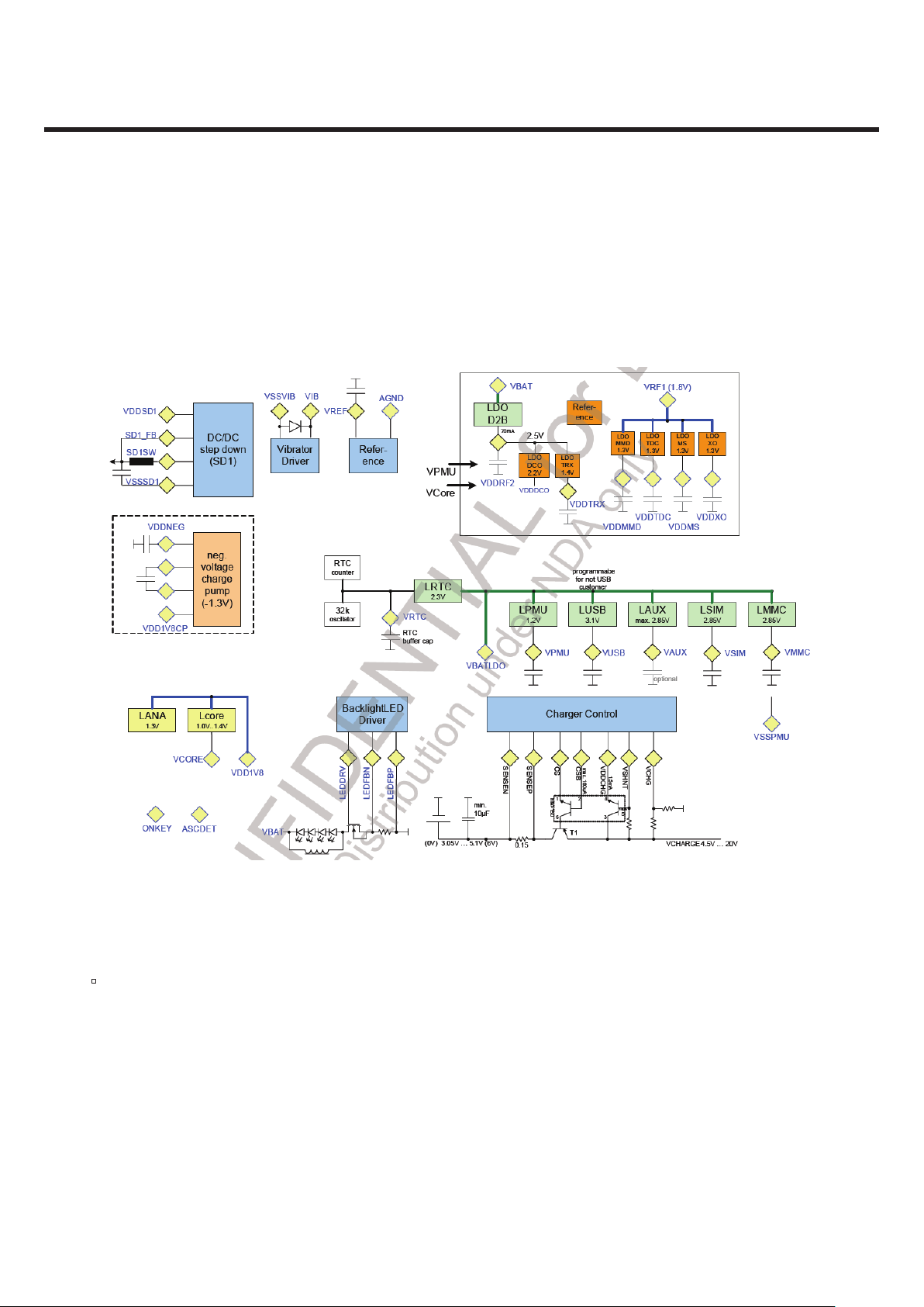
3.3 Power Management
A mobile platform requires power supplies for different functions. These power supplies are generated in the
integrated power management Unit (PMU). The PMU is designed to deliver the power for a typical standard
phone.
Figure. 3-2-1 Block Figure of the PMU Modules X-Gold tm 215
DC/DC Step Down Converter for 1.8V (SD1)
The DC/DC converter generates a 1.8V supply rail. This voltage rail is used to supply main parts of the system,
like the digital core of the chip (via LDO LCORE), some parts of the mixed signal macro, parts of the RF macro
and the external memory if a 1.8V memory is used. The efficiency of the DC/DC converter is optimized for an
average load current of 100mA. That is the load current estimated for the GSM talk mode.

3. TECHNICAL BRIEF
Linear voltage Regulators (low dropout) LDOs
The LDOs are used to generate the supply for the different supply domains not directly supplied out of the
DC/DC converter.
LCORE
The LCORE LDO provides the VCORE supply used for most of the digital parts of the chip
LPMU
The LPMU provides VPMU sued for the PMU supply, e.g. for the startup state machine and analog parts like
ADC, sense amplifier etc.
LUSB
The LUSB LDO generates the supply for the USB transceiver (output driver and input). If no USB interface is
required, LUSB can be used as general purpose LDO.
LAUX
The LAUX generates VAUX. It is a general purpose LDO and can be used for different functions depending on
the phone application, e.g. for the display or Camera.
LMMC
The LMMC generates VMMC. It is a general purpose LDO and can be used e,g. for memory cards
LSIM
The LSIM LDO generates the VSIM supply for the SIM card and interface. It is designed to supply Standard SIM
cards according ETSI TS 102 221.
Other LDOs
• The RF module has implemented several LDO’s for different RF power domains.
• The mixed signal module has some LDO’s for the audio driver and microphone supply
• The FM receiver has an internal LDO for sensitive RF circuits.
LGE Internal Use Only Copyright © 2011 LG Electronics. Inc. All right reserved.
- 21 -
Only for training and service purposes
- 22 -
LGE Internal Use Only Copyright © 2011 LG Electronics. Inc. All right reserved.
Only for training and service purposes
3. TECHNICAL BRIEF
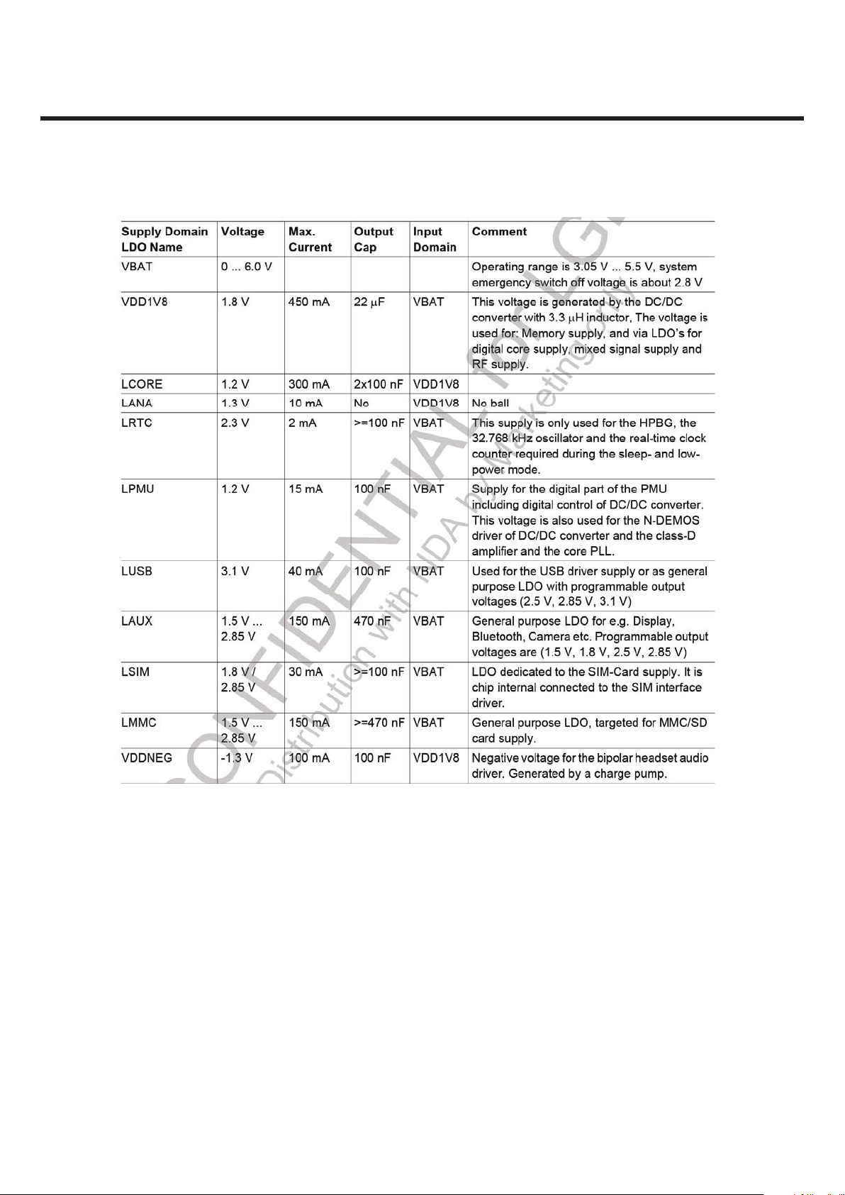
Table. 3.3.1 Power supply Domains (without RF)

3. TECHNICAL BRIEF
3.3.1 Power on and startup
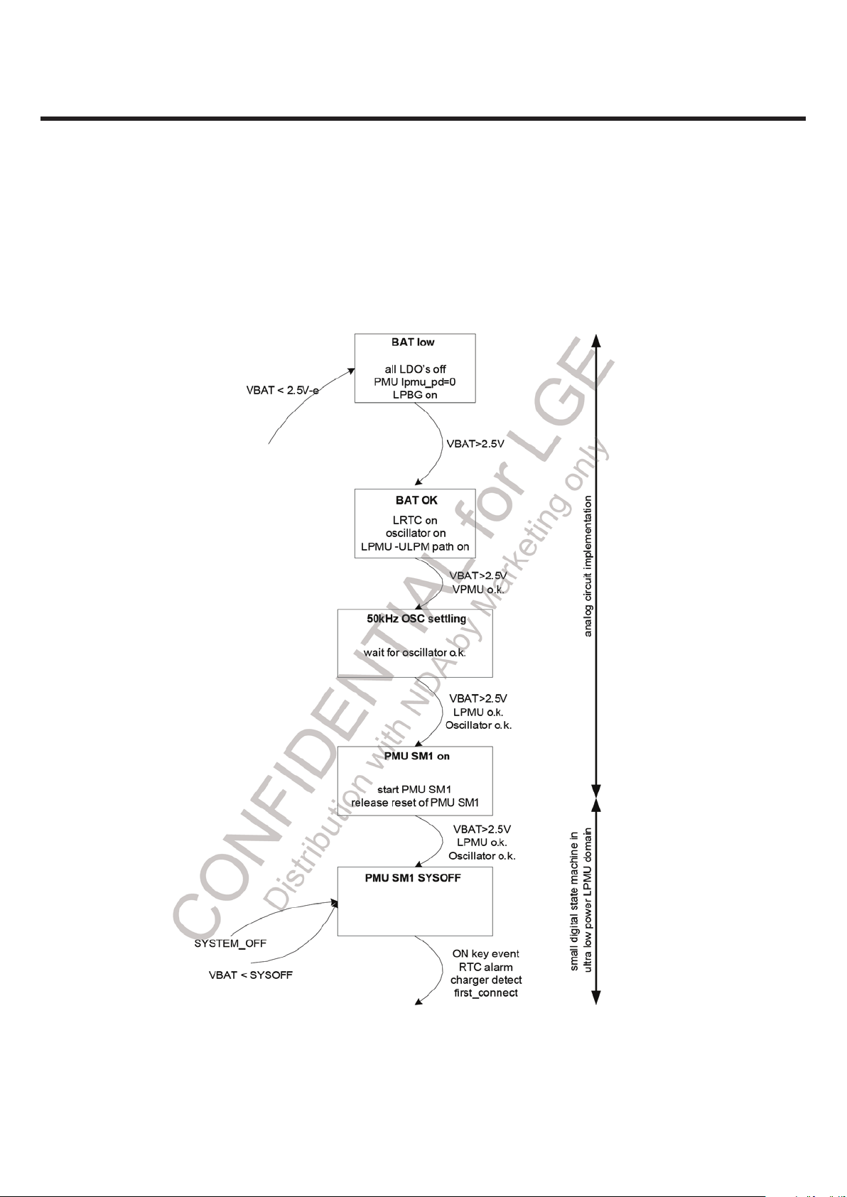
Analog startup Circuit
Because the POR circuit and the LPBG are directly connected to the battery, it is not possible to switch them
off. If the battery voltage exceed the power on reset threshold (2.5V), the power on reset is released, the LPMU
regulator and the LRTC voltage regulator are switched on. The LPMU regulator starts in its ultra-low power
mode
The LPMU regulator generates a control signal (lpmu_OK) that enables the 50KHZ PMU oscillator. The output
clock of the oscillator is checked with a fully coded counter. A counter overflow releases the reset
(vpmu_rst_n) signal for the small PMU state-machine.
Small first digital State-Machine
The small PMU state-machine is always connected to VPMU After starting from reset the small startup state
machine enters the SYSTEM OFF state and only continuous the startup procedure if a switch on event like first
connect, on-key, wake up or charge detect occurs.
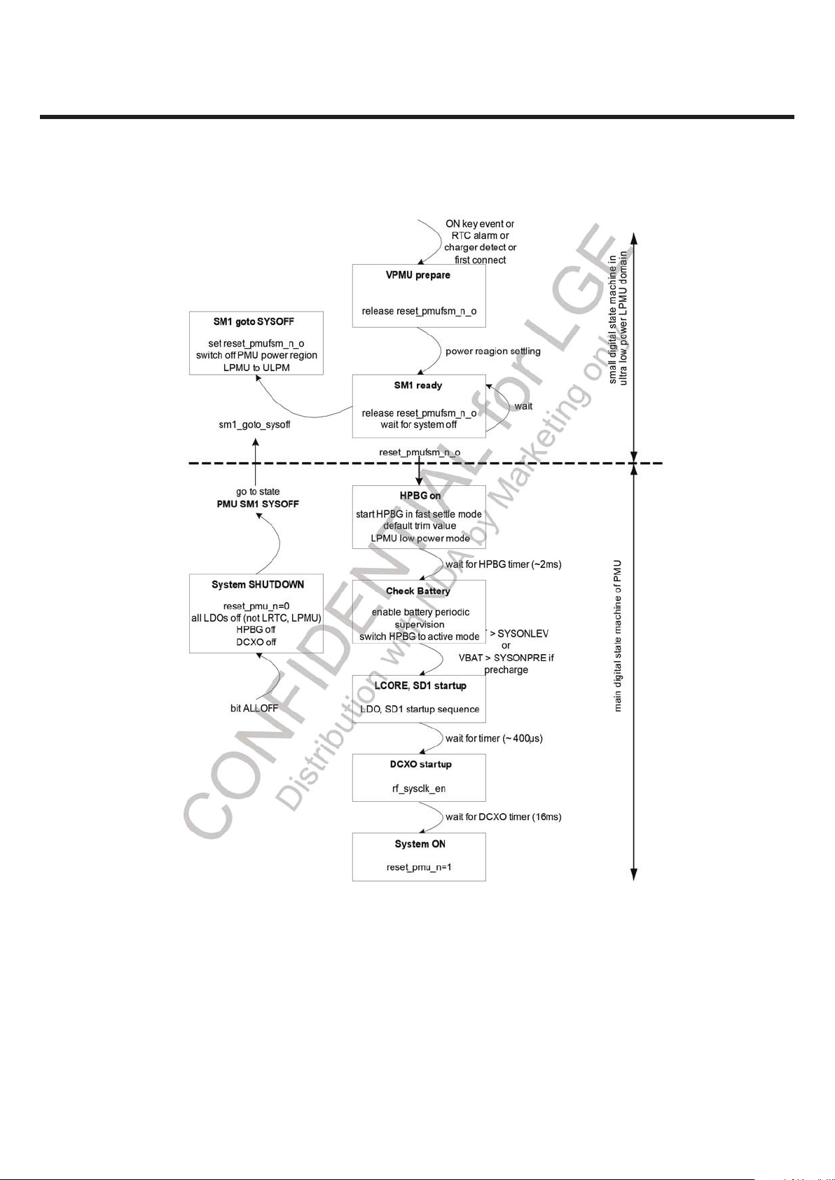
PMU-main State-Machine
The main PMU state-machine is always connected to VPMU also. The power up sequence driven by the PMU
state-machine can be seen in Figure18. After enabling the reference (HPGB) and waiting for the settling time,
the battery voltage is measured and compared with the power on threshold. If the battery voltage is high
enough, the SD1 DC/DC converter and the LCORE LDO are started. A timer ensures that the supply voltage
will be stable before the DCXO is enabled. The DCXO settling time is ensured using a fixed timer. After an
overflow of this timer, the reset is released for the rest of the system. The PMU state machine remains in this
System-ON state until the system is switched into the OFF state. For example the system sleep mode is
completely configured by software( for example switching off the LDO’s, switching of the DCXO etc.) and
controlled by the VCXO_enable signal. The reason for the startup is stored in the ResetSourceRead register.
Battery Measurement
LGE Internal Use Only Copyright © 2011 LG Electronics. Inc. All right reserved.
- 23 -
Only for training and service purposes
- 24 -
LGE Internal Use Only Copyright © 2011 LG Electronics. Inc. All right reserved.
Only for training and service purposes
3. TECHNICAL BRIEF
The ADC and the oscillator for the ADC needs the VDD_ADC supply voltage from the LADC LDO. LADC uses
either the charger voltage VDD_CHARGE or VDDRTC as input voltage. The input voltage is selected
automatically by a bulk switch circuit. LADC, the ADC and the oscillator are enabled on request for every battery
measurement if the charger unit is not running. This is handled by an ADC control block in one of the statemachines. If the charger unit is running the ADC is controlled by the charger state-machine
Figure.3.3.2 First Part of the State Machine, Running in Different Power Domains than the Second Part
3. TECHNICAL BRIEF
Figure 3.3.3 Second (Main) Part of the Startup State Machine in the VPMU Domain
LGE Internal Use Only Copyright © 2011 LG Electronics. Inc. All right reserved.
- 25 -
Only for training and service purposes

- 26 -
LGE Internal Use Only Copyright © 2011 LG Electronics. Inc. All right reserved.
Only for training and service purposes
3. TECHNICAL BRIEF
3.3.2 Switching on due to first connect
If the battery voltage is connected the first time, that means the system enters the first time the SYSOFF state,
this is stored in a first connect flag. If the first connect flag is set, the system will start immediately and not wait
for any other system on event in the SYSOFF state.
3.3.3 Switching on due to on-Key event
The on key is connected to the ONKEY pad. The ESD protection and the input structure of this pad are
connected to VRTC. If the ONKEY pad is forced to VRTC by an external key or similar circuit, the system starts.
The ONKEY is sampled with the PMU clock. It has to be sampled four times high before a valid on event is
generated. The status of the ON key can be read in the PMU registers, so it can be used as a functional key
during phone operation also
3.3.4 Switching on due to RTC alarm
The real time clock can generate a wakeup signal called RTC alarm. This signal is sampled from the state-
machine and after successfully detecting a high, the system is switched on.
3.3.5 Switching on due to charging
When a battery with a voltage below the SSONLEV level is inserted, the state machine will not start the system.
As long as the battery voltage stays lover than SYSONLEV the system will stay off. The only possibility to start
up the system is due to an external charger.
If an external charger is connected and detected and the battery is charged above the SYSONPRE voltage level
the system will start up.
The PMU main state machine waits in the Check battery state until the battery voltage condition is fulfilled.
The charger state machine provides the necessary pre-charge indication signal. This pre-charge signal is
denounced in a small counter to have a stable signal. This is important, especially in half/full-wave charging
where the charger detection is switching between charger detected/not detected according the AC supply
frequency. reasons
For details on pre-charging see the charger chapter. The charger is controlled by an independent state
machine. The pre-charge signal is used to trigger the pre-charge signal is used to trigger the pre-charge
functionality. The charger state machine fully control the pre-charge, the PMU-state machine now changes to
state HPBG on state and the system starts. This state change is indicated to the charger state-machine to
enable the charger watchdog for safety

3. TECHNICAL BRIEF
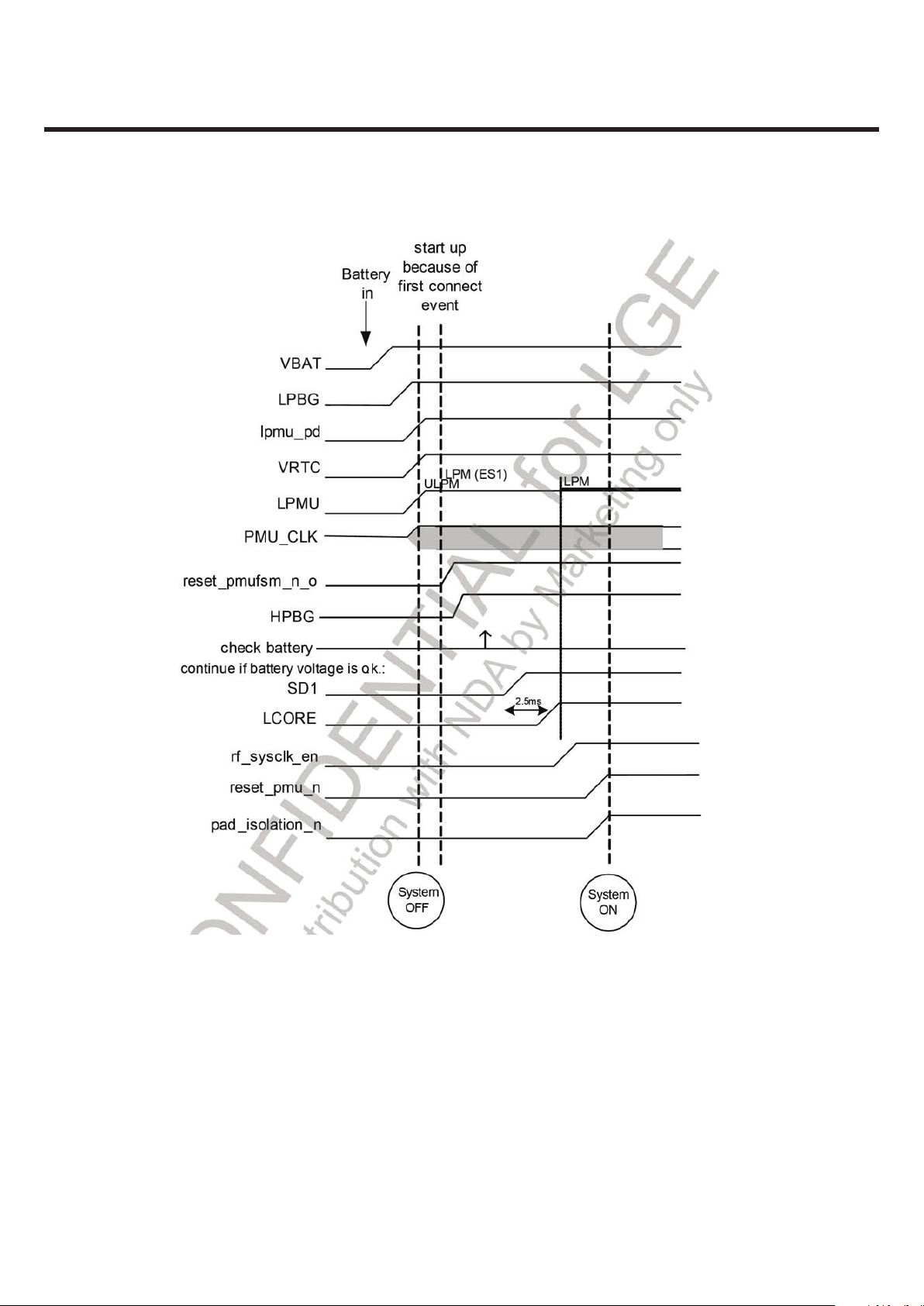
3.3.6 Power Supply Start-up sequence
In order to avoid an excessive drop on the battery voltage caused by in-rush current during system power-on,
possibly leading to system instability and “hick-ups” a staggered turn-on approach for the regulators is
implemented. The regulators are turned on in a well defined sequence, thus spreading the in-rush current
transients over time.
The IO’s of X-GOLD TM 215 are isolated in OFF mode (core supply is off). The isolation signal is controlled by
the PMU state machine. This ensures that the PADs are in a well defined state during core supply settling. This
allows to power up the LCORE core regulator and wait for the core to reach reset state before powering up the
I/O supply regulators.
LGE Internal Use Only Copyright © 2011 LG Electronics. Inc. All right reserved.
- 27 -
Only for training and service purposes
- 28 -
LGE Internal Use Only Copyright © 2011 LG Electronics. Inc. All right reserved.
Only for training and service purposes
3. TECHNICAL BRIEF
Figure 3.3.4 Start Up Sequence (triggered by First Connect Event)

3. TECHNICAL BRIEF
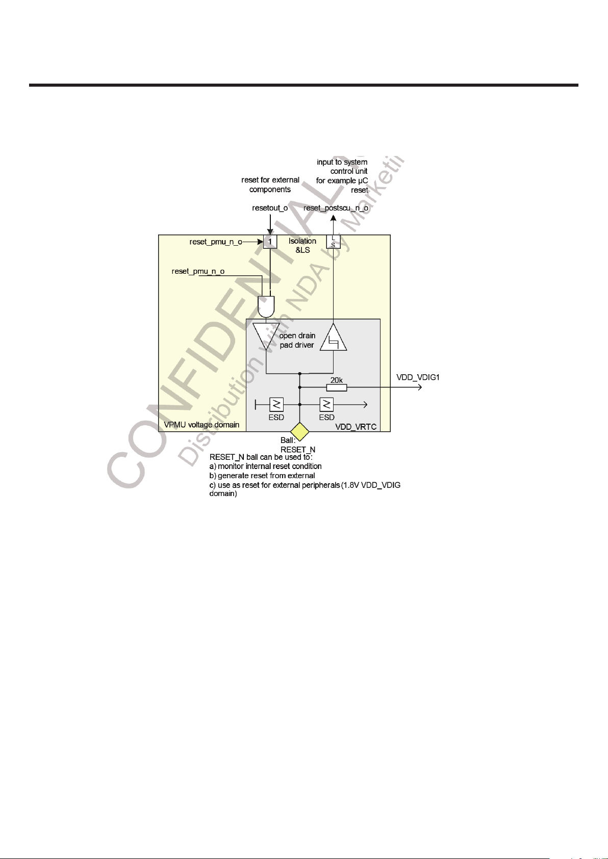
3.3.7 External Reset Handling
The chip reset can be controlled by an external RESET_N ball. If this ball is pulled low, the chip will be reset.
All PMU registers are reset during the external reset including LSIM control bits. The PMU statemachines are
also not reset from the external reset. An SW or watchdog reset will not reset the PMU registers. A SW and
Watchdog reset is seen on the reset_n pad to allow the reset of external devices. Basically there are three reset
sources, first the reset signal controlled by the PMU (reset_pmu_n_o), second the reset signal controlled by the
SCU (resetout_o) and third the external reset (RESET_N). The SCU reset is triggered by SW (for example due to a
SW reset or watchdog reset). The PMU reset is controlled by the PMU state machine. The output of the reset
handling block is the reset_postscu_n_o signal. This signal controls for example the ɆC subsystem and releases
reset for the controller. During normal start up, the PMU releases the reset_pmu_n_o signal after entering the
SYSTEM ON state. At this time the resetout_o signal is high, the RESET_N pad is not pulled low and therefore
the reset_postscu_n_o signal follows the reset_pmu_n_o signal. That means the ɆC reset will be released and
the ɆC starts operation. If the SW triggers an external reset via the SCU, signal resetout_o will be forced to low
for a certain time and RESET_N will be forced to low by the open drain driver. At the same time the feedback to
the SCU will be masked to not reset the baseband. The RESET_N pad is in the VDDRTC domain but the internal
pull up is connected to the VDD_VDIG1 (1.8V) domain. That allows the pad to be used as reset for external
devices running in the VDD1V8 domain. The RESET_N pad can also be used to monitor the chip internal reset
condition during startup.
The open drain driver is a weak driver, that means it can be forced to high during debug from external pushing
some current into the pad. In testmode signal reset_pmu_n_o is high, that means the chip reset is fully
controlled from external
LGE Internal Use Only Copyright © 2011 LG Electronics. Inc. All right reserved.
- 29 -
Only for training and service purposes
- 30 -
LGE Internal Use Only Copyright © 2011 LG Electronics. Inc. All right reserved.
Only for training and service purposes
3. TECHNICAL BRIEF
3.3.8 Sysclock Switching
The PMU controls the rf_sysclk_en signal of the DCXO in the RF macro. During startup the PMU enables the
DCXO. After the system is running the DCXO is controlled by the SCU of the baseband by using the
vcxo_enable signal. This is handled by a dedicated logic in the PMU, see Figure 3.3.6. As long as
rf_sysclk_en_pmu, the output of the PMU state-machine is high, vcxo_enable controls the rf_sysclk_en signal
to the RF. If rf_sysclk_en_pmu is low, the DXCO is switched off, independent from vcxo_enable.
Figure 3.3.5 PMU, CGU and External Reset
 Loading...