

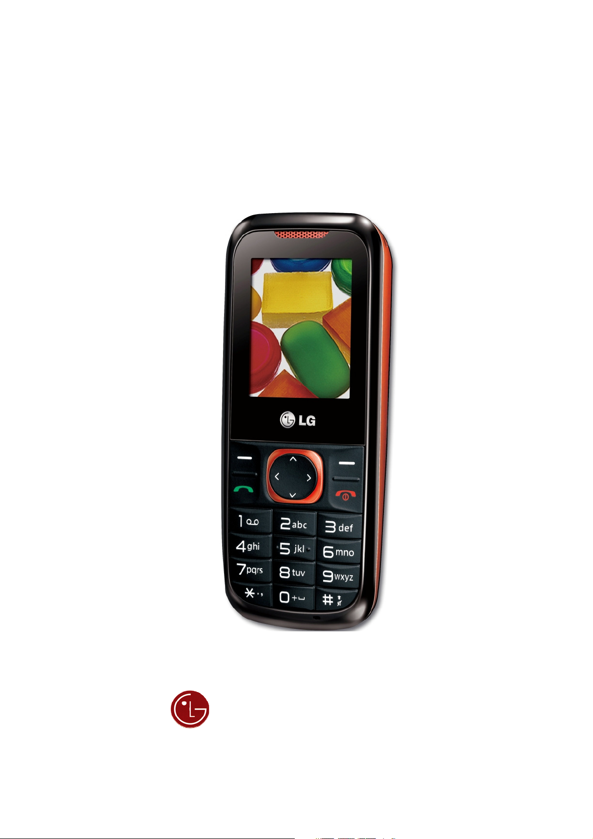
LG Electronics
LG-A120
Service Manual
1

Table Of Contents
1. INTRODUCTION…………………...3
1.1 Purpose…………………………………3
1.2 Regulatory Information………………..3
2. PERFORMANCE…………………..5
2.1 H/W Features…………………………..5
2.2 S/W Features…………………………..6
3. TECHNICAL BRIEF………………14
3.1 Digital Main Processor(
3.2 Power Amplifier Module(
3.3 Transceiver Module(
3.4 Memory Module (
3.5 FM Radio Module (
3.6 LCD Interface………………………....32
3.7 SIM Card Interface…..……………….34
3.8 KEYPAD Interface……………….…...35
3.9 Battery Charging Block Interface…...36
3.10 Audio Interface……………….….…..37
K5L6443ABM-AD11)
MT6223
SKY77542
AD6548
)…………..23
AR1200/1210
)……….14
)…....22
….....26
)…….….30
4.14 Torch LED Trouble…………….75
4.15 FM Radio Trouble……………..77
4.16 No Connection Trouble……….80
4.17 RX Trouble…………………..…83
4.18 DCXO Trouble…………………86
4.19 SAW Filter Trouble……………87
4.20 TX Trouble……………………..88
4.21 Transceiver trouble……………90
4.22 PAM Trouble…………………...91
4.23 Mobile Switch Trouble………...96
5. DOWNLOAD………………....98
5.1 Download setup…………………98
5.2 Download Process……………...99
6. BLOCK DIAGRAM………….107
7. CIRCUIT DIAGRMA………...108
3.11 Vibrator Interface….………………...38
3.12 Key LED Interface……………….….39
4. TROUBLE SHOOTING…………..40
4.1 Power On Trouble……………………40
4.2 SIM Card Trouble…………………….43
4.3 Vibrator Trouble………………………45
4.4 Keypad Trouble……………………….47
4.5 RTC Trouble…………………………..50
4.6 Key Backlight Trouble………………..52
4.7 LCM Backlight Trouble…………….…55
4.8 LCM Trouble……………….……….…58
4.9 Microphone Trouble…………………..61
4.10 Receiver Trouble…………………….64
4.11 Speaker Trouble……………………..66
4.12 Headphone Trouble………….……...69
4.13 Charging Trouble…………………....73
8. BGA IC PIN Check…………114
9. PCB LAYOUT……………….116
10.ENGINEERING MODE……118
11. CALIBRATION…………….122
11.1 Test Equipment Setup……….122
11.2 Calibration Steps……………..123
12. STAND ALONE TEST…….162
12.1 Test Configuration……………162
12.2 META tool Install process…...163
12.3 Rx Test………………………...166
12.4 Tx Test…………………………172
13. #EV#………………………...178
2

1. INTRODUCTION
1.1 Purpose
This manual provides information necessary to repair, description and download the features
of this model.
1.2 Regulatory Information
A. Security
Toll fraud, the unauthorized use of telecommunications system by an unauthorized part(for
example ,persons other than your company’s employees, agents, subcontractors, or person
working on your company’s behalf) can result in substantial additional charges for your
telecommunications services.
System users are responsible for the security of own system. There are may be risks of toll
fraud associated with your telecommunications system. System users are responsible for
programming and configuring the equipment to prevent unauthorized use .The manufacturer
dose not warrant that this product is immune from the above case but will prevent unauthorized
use of common-carrier telecommunications service of facilities accessed through or connected
to it.
The manufacturer will not be responsible for any charges that result from such unauthorized
use.
B. Incidence of Harm
If a telephone company determines that the equipment provided to customer is faulty and
possibly causing harm or interruption in service to the telephone network, it should disconnect
telephone service until repair can be done. A telephone company may temporarily disconnect
service as long as repair is not done.
C. Changes in Service
A local telephone company may make changes in its communications facilities or procedure. If
these changes could reasonably be expected to affect the use of the this phone or compatibility
with the network, the telephone company is required to give advanced written notice to the user,
allowing the user to take appropriate steps to maintain telephone service.
D. Maintenance Limitations
Maintenance limitations on this model must be performed only by the manufacturer or its
authorized agent . The user may not make any changes and/or repairs expect as specifically
noted in this manual.
Therefore, note that authorized alternations or repair may affect the regulatory status of the
system and may void any remaining warranty.
3

E. Notice of Radiated Emissions
This model complies with rules regarding radiation and radio frequency emission as defined
by local regulatory agencies. In accordance with these agencies, you may be required to provide
information such as the following to the end user.
F. Pictures
The pictures in this manual are for illustrative purposes only; your actual hardware may look
slightly different.
G. Interference and Attenuation
Phone may interfere with sensitive laboratory equipment, medical equipment, etc.
Interference from unsuppressed engines or electric motors may cause problems.
H. Electrostatic Sensitive Devices
ATTENTION
Boards, which contain Electrostatic Sensitive Devices(ESD),are indicated by the
sign .
Following information is ESD handing:
. Service personnel should ground themselves by using a wrist strap when exchange system
boards.
. When repairs are made to a system board , they should spread the floor with anti-static mat
which is
also grounded .
. Use a suitable, grounded soldering iron .
. Keep sensitive parts in these protective packages until these are used.
. When returning system boards or parts like EEPROM to the factory, use the protective
packages as
described.
4
2. PERFORMANCE
2.1 H/W Features
Solution 6223D MTK
Type Bar type
Antenna Type Internal (dual-Band)
Main Display 1.77” 128 x 160 , TFT/65k
Battery 950mAh Li-ion inner pack 950mAh: 55x34x5.7mm
Music player Yes
FM Receiver Yes , US/Europe band support
Embedded FM antenna Yes
Real time FM recording Yes
Loud Speaker Yes
Music player--real resuming Yes
Memory Size 64Mb+32Mb User memory: 729KB
LMT (Lost Mobile Tracker) Yes
Torch LED Y
In flight mode Yes
Only for FM (AMR/WAV
file)
(87.5~108MHz)
Tension contact FPC
type FM Antenna on
Battery cover.
x 2 , Φ16 speaker
LMT for: AMA
M-DOG: China
5

2.2 S/W Features
Feature Detail Item Description
OS OS Operating System Y
Audio
Speech Code FR,EFR,HR,AMR-NB Y
AMR code GSM Full Rate
3GPP Adaptive Multi Rate (AMR-NB)
FM Radio Y
MP3 Ring
Tone
Integrated hands
free
speaker
Key Tone
Volume
Ring Tone
Volume
Ring Tone MP3 ring tone/Midi Y
Call Alert
type
MP3 decode Y
Speaker phone mode Y
6 Level (Include Mute) Y
6 Level (Include Mute) Y
Ring, Vibrate, Ring & Vibrate, Ring after
vibrate, Silent
Y
Y
Bands
Connectivity
Earpiece
Volume
Mute Y
GSM dual
band MS
900-1800
PCS dual
band MS
850-1900
Circuit N Date Service
Packet N
Infrared
(IrDA)
Bluetooth N
USB N
USB Mass
6 Level (Include Mute) Y
Configuration is during software compile
time.
N
N
N
Y Frequency
storage
RS232(UAR
T)
Only for manufacture tool Y
6
Voice
Voice
Y
Function
Camera
Recording
Voice
Command
Answering
machine
Capture Size 160x120, 320x240, 640x480 N
Preview Size Full Screen: 128x128 N
Quality Low, Normal, High N
EV +4, +3, +2, +1, 0, -1, -2, -3, -4 N
WB Auto, Daylight, Tungsten,
Zoom 640x480 : 1x
Effect Normal, Sepia, Grayscale, Color invert N
N
N
N
FLUORESCENT, Cloud,
INCANDESCENCE
N
320x240 : 1x, 2x
160x120/128x128 : 1x, 2x, 4x
File Manager
(Sound folder)
Continuous
Shot
Self Timer 3 seconds, 5 seconds, 10 seconds N
Shutter tone Off, tone1, tone2, tone3 N
Storage Phone/SD card N
Reset Setting Restore to default setting N
Browse detail
image Info
Full Screen
View
Browse file
tree
Copy,
Rename,
Delete, Move
files
1 Shot, 3 shot, 6 shot N
N Image Viewer
N
Y
Y
Rename,
Delete,
Multi-Delete,
Create folder
Display RSSI 6 level (0~5 level) Y
Y
7
Battery level 4 level (0~3 level) Y
RTC Date & Time Display Y
Call History
PLMN/Servic
e Indicator
Quick Access
Mode In Idle
Dimming
Clock
Dual Clock N
Home
shortcut
Last Dial
Number
Last
Received
Number
Last Missed
Number
Y
Y
N
Display Shortcut icon in Idle(Quick
Access)
Max : 40 records Y
Max : 40 records Y
Max : 40 records Y
Y
Call
Management
Scratch Pad
Memory
Call Duration Last Call time, Total Call Time Y
Last Call
Charge Units
Total Charge
Units
Call Waiting Y
Call Swap Y
Call Retrieve Y
Auto Answer N
Auto Redial Y
Calling Line N
Full Call
Divert
Speed
N
Y Call Cost
Y
Y
Y
Dialing
Last Number
Redial
Y
8
Multi Party
Call
ECT Explicit Call Transfer Y
Y
Network
Cell Broadcast
Automatic Network
Selection
Manual
Network
Preferred
Network
Network
Service
Status
DTMF
Signaling
DTMF
Enable &
Disable
Read Cell
Broadcast
Y
Y
(User definition) Y
Y
Y DTMF
Y
Y
Contacts(Pho
ne Book)
On/Off
setting
Alert setting N
CB message
Language
setting
Channel
Setting
Entry 1000 Y
Field Name, Mobile, Home, Office Y
Copy ME <-> SIM Y
Move ME <-> SIM Y
FDN Y
SDN Y
Email Entry N
Picture ID N
Receive On/Off Y
Y
Y
Video Caller
ID
vCard N
N
9
Business
Card
N
Supplementary
Services
Delete Delete, Delete All(SIM or Phone), Multi
Delete
CFU Call Forwarding Unconditional Y
CFB Call Forwarding on Mobile Subscriber
Busy
CFNRy Call Forwarding on No Reply Y
CFNRc Call Forwarding on Mobile Subscriber
Not Reachable
BAOC Barring of All Outgoing Calls Y
BOIC Barring of Outgoing International Calls Y
BOICexHC Barring of Outgoing International Calls
except those directed to the Home
PLMN Country
BAIC Barring of All Incoming Calls Y
BICRoam Barring of Incoming Calls when
Roaming Outside the/Home PLMN
Y
Y
Y
Y
Y
SIM
Short
Message
Country
Conference
Call
Plug in Type 3V & 1.8 V Y
SIM Lock Service Provider / Network Lock N
SIM Toolkit Class 3 Y
Read
Message
Write and
Edit Message
Send and Receive
Message
Reply to
Message
Forward
Message
Up to 5 Y
Y
Y
Y
Y
Y
Extract Number
from
Message
Y
10
Message
Status
Y
Message
Unread
Settable Message
Center Number,
Reply Path
and Validity
Visible and Audible
Message
Receive
Voice Mail Y
Settable Voice Mail
Center
Number
Message
Protocol
Message Overflow
Y
Y
Y
Y
Normal, Y
Blinking Icon Y
Miscellaneous
Function
Indicator
Message
Center
Number
Nokia Smart
Message
Development &
Test
Facility
Field Test
Facility
Display
Software
Version
IMEI Y
Restore
Y
N
Y
Y
Y
Y
Factory
Setting
11
Battery
Charging
Mode
Language Selectable Auto Language Y Text Input
Y
Predictive
word input
Scheduler
World Time
Unit converter Length, Weight, Y
Stop Watch N
Calculator + - * / Y
Calendar MAX: 100 records (35 chars) Y
To Do MAX: 50 records (35 chars) Y
Memo MAX: 10 records (80 chars) N
Setting Local
Time
Display Two
Number of
Cities Time
Daylight
saving
NITZ Y
T9 Y
Y
Dual Clock N
Y
Phone Book
Sync
Message
Sync
Game 2 C game Y
Security
Real Time
Clock
Emergency
Call
Handset
Lock
Security
Code
PIN Lock Y
Keypad Lock Y
12/24 Hour Y
Calendar Y
Time Zone Y
Only For manufacture N PC Sync
N
Y
Y
When Delete All N
Daylight
saving
12
N

Alarm
Once, Daily, Mon~Fri, hourly Y
Manager
Dimming
Clock
Power-off
Alarm
On Alarm
Event
Mobile
Tracking
software
M-DOG For China Y
Accessory Charger
Adapter
Normal
earmic
(without hook
switch)
N
Y
Display & Ring Y
For India, Asia Y Others
Y
Y
User Memory 729 KB Y
13
3. TECHNICAL BRIEF
3.1 Digital Main Processor
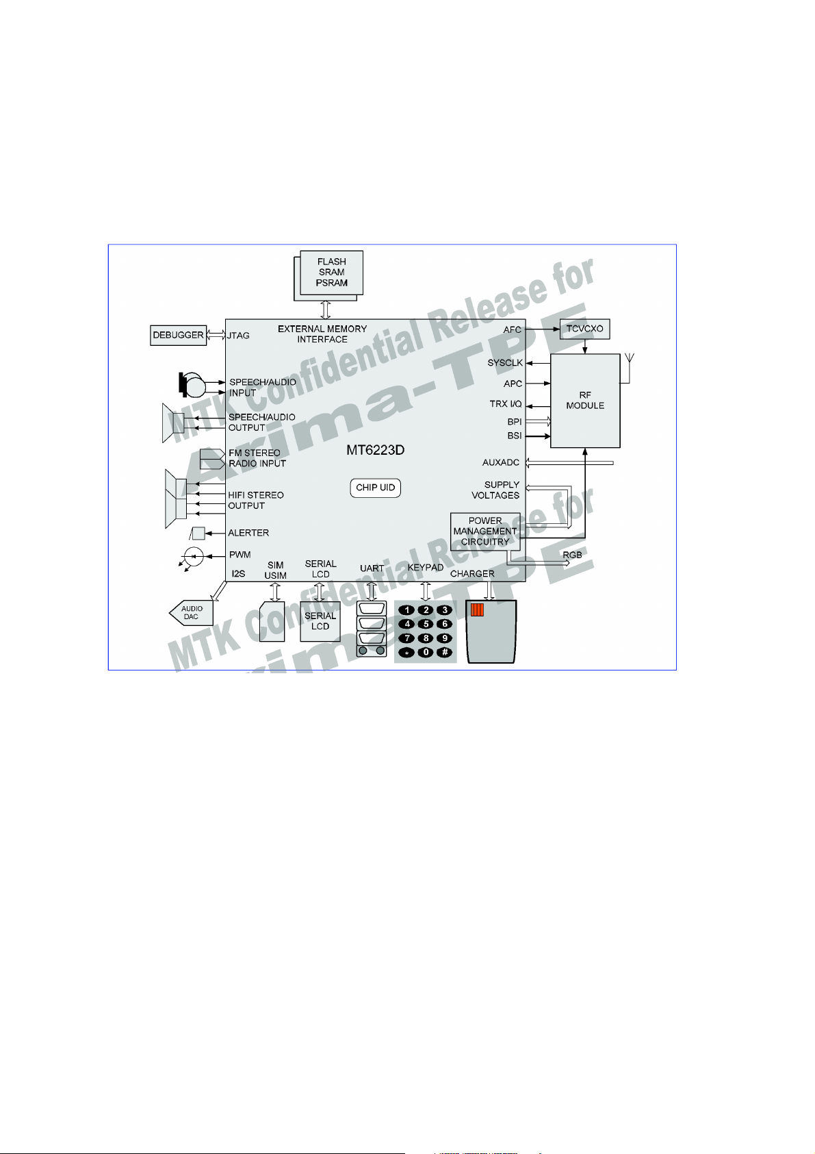
Figure.3-1-1 MT6223 FUNCTIONAL BLOCK DIAGRAM
14

3.1.1 System Overview
MT6223D is an entry level chipset solution with class 12 GPRS/GSM modem. It integrates not
only analog baseband but also power management blocks into one chip and can greatly reduce the
component count and make smaller PCB size. Besides, MT6223D is capable of SAIC (Single
Antenna Interference Cancellation) and AMR speech.
Based on 32 bit ARM7EJ-STM RISC processor, MT6223D provides an unprecedented
platform for high quality Modem performance.
Platform
MT6223D runs the ARM7EJ-STM RISC processor at up to 52Mhz, thus providing best trade-off
between system performance and power consumption.
For large amount of data transfer, high performance DMA (Direct Memory Access) with
hardware flow control is implemented, which greatly enhances the data movement speed while
reducing MCU processing load.
Targeted as a modem-centric platform for mobile applications, MT6223D also provides hardware
security digital rights management for copyright protection. For further safeguarding, and to protect
manufacturer’s development investment, hardware flash content protection is also provided to
prevent unauthorized porting of software load.
Memory
MT6223D supports up to 2 external state-of-the-art devices through its 16-bit host interface.
Devices such as burst/page mode Flash, page mode SRAM, and Pseudo SRAM are supported. To
minimize power consumption and ensure low noise, this interface is designed for flexible I/O
voltage and allows lowering of supply voltage down to 1.8V. The driving strength is configurable for
signal integrity adjustment. The data bus also employs retention technology to prevent the bus
from floating during turn over.
Multi-media
MT6223D utilize high resolution audio DAC, digital audio, and audio synthesis technology to
provide superior audio features., e.g. MP3 ring tone.
Connectivity, and Storage
MT6223D supports UART as well as Bluetooth interface. Also, necessary peripheral blocks are
embedded for a voice centric phone: Keypad Scanner with the capability to detect multiple key
presses, SIM Controller, Alerter, Real Time Clock, PWM, Serial LCD Controller, and General
Purpose Programmable I/Os.
Audio
Using a highly integrated mixed-signal Audio Front-End, architecture of MT6223D allows for
easy audio interfacing with direct connection to the audio transducers. The audio interface
integrates D/A and A/D Converters for Voice band, as well as high resolution Stereo D/A
Converters for Audio band. In addition, MT6223D also provides Stereo Input and
Analog Mux. MT6223D also supports AMR codec to adaptively optimize speech and audio quality.
15

Radio
MT6223D integrates a mixed-signal Baseband front-end in order to provide a well-organized
radio interface with flexibility for efficient customization. It contains gain and offset calibration
mechanisms, and filters with programmable coefficients for comprehensive compatibility control on
RF modules. This approach also allows the usage of a high resolution D/A Converter for controlling
VCXO or crystal, thus reducing the need for expensive TCVCXO. MT6223D achieve great
MODEM performance by utilizing 14-bit high resolution A/D Converter in the RF downlink
path. Furthermore, to reduce the need for extra external current-driving component, the driving
strength of some BPI outputs is designed to be configurable.
Debug Function
The JTAG interface enables in-circuit debugging of software program with the ARM7EJ-S core.
With this standardized debugging interface, MT6223D provides developers with a wide set of
options in choosing ARM development kits from different third party vendors. Low Power Features
MT6223D offers various low-power features to help reduce system power consumption. These
features include Pause Mode of 32KHz clocking at Standby State, Power Down Mode for individual
peripherals, and Processor Sleep Mode. In addition, MT6223D are also fabricated in advanced low
leakage CMOS process, hence providing an overall ultra low leakage solution.
Power Management
MT6223D integrates all regulators that a voice-centric phone needs. Seven LDOs optimized for
Specific GSM/GPRS baseband sub-systems are included, and a RF transceiver needed LDO is
also built-in. Besides Li-Ion battery charge function, SIM card level shifter interface, two open-drain
output switches to control the LED and vibrator are equipped. Other power management schemes
such as thermal overload protection, Under Voltage Lock-out Protection (UVLO), over voltage
protection and oower-on reset and start-up timer are also MT6223D features. Besides, 3 NMOS
switches controlling the RGB LEDs are also embedded to reduce BOM coount.
Package
The MT6223D device is offered in 9mm×9mm, 224-ball,
0.5 mm pitch, TFBGA package.
3.1.2 Platform Feature
General
Integrated voice-band, audio-band and base-band analog front ends
TFBGA 9mm×9mm, 224-ball, 0.5 mm pitch package
MCU Subsystem
ARM7EJ-S 32-bit RISC processor
High performance multi-layer AMBA bus
Java hardware acceleration for fast Java-based games and applets
Operating frequency: 26/52 MHz
16

Dedicated DMA bus
7 DMA channels
320K bits on-chip SRAM
On-chip boot ROM for Factory Flash Programming
Watchdog timer for system crash recovery
3 sets of General Purpose Timer
Circuit Switch Data coprocessor
Division coprocessor
External Memory Interface
Supports up to 2 external devices
Supports 16-bit memory components with maximum size of up to 128M Bytes each
Supports Flash and SRAM/PSRAM with Page Mode or Burst Mode
Industry standard serial LCD Interface
Supports multi-media companion chips with 8/16 bits data width
Flexible I/O voltage of 1.8V ~ 2.8V for memory interface
Configurable driving strength for memory interface
User Interfaces
5-row × 7-column keypad controller with hardware scanner
Supports multiple key presses for gaming
SIM/USIM Controller with hardware T=0/T=1 protocol control
Real Time Clock (RTC) operating with a separate power supply
General Purpose I/Os (GPIOs)
2 Sets of Pulse Width Modulation (PWM) Output
Alerter Output with Enhanced PWM or PDM
6 external interrupt lines
Security
Supports security key and 59 bit chip unique ID
Connectivity
3 UARTs with hardware flow control and speed up to 921600 bps
DAI/PCM and I2S interface for Audio application
Low Power Schemes
Power Down Mode for analog and digital circuits
Processor Sleep Mode
Pause Mode of 32KHz clocking at Standby State
3-channel Auxiliary 10-bit A/D Converter for application usage other than battery monitoring
Power and Supply Management
2.8V to 5.5V Input Range
Charger Input up to 8V
Seven LDOs Optimized for Specific GSM
17

Sub-systems
One LDO for RF transceiver
High Operation Efficiency and Low Stand-by Current
Li-Ion Battery Charge function
SIM Card Interface
Two Open-Drain Output Switches to Control the LED and Vibrator
Three NMOS switches to control RGB LEDs
Thermal Overload Protection
Under Voltage Lock-out Protection
Over Voltage Protection
Power-on Reset and Start-up Timer
Test and Debug
Built-in digital and analog loop back modes for both Audio and Baseband Front-End
DAI port complying with GSM Rec.11.10
JTAG port for debugging embedded MCU
3.1.3 MODEM Features
Radio Interface and Baseband Front End
GMSK modulator with analog I and Q channel outputs
10-bit D/A Converter for uplink baseband I and Q signals
14-bit high resolution A/D Converter for downlink baseband I and Q signals
Calibration mechanism of offset and gain mismatch for baseband A/D Converter and D/A
Converter
10-bit D/A Converter for Automatic Power Control
13-bit high resolution D/A Converter for Automatic Frequency Control
Programmable Radio RX filter with adaptive bandwidth control
Dedicated Rx filter for FB acquisition
2 Channels Baseband Serial Interface (BSI) with 3-wire control
Bi-directional BSI interface. RF chip register read access with 3-wire or 4-wire interface.
10-Pin Baseband Parallel Interface (BPI) with programmable driving strength
Multi-band support
Voice and Modem CODEC
Dial tone generation
Voice Memo
Noise Reduction
Echo Suppression
Advanced Sidetone Oscillation Reduction
Digital sidetone generator with programmable gain
18

Two programmable acoustic compensation filters
GSM/GPRS quad vocoders for adaptive multirate (AMR), enhanced full rate (EFR), full rate
(FR) and half rate (HR)
GSM channel coding, equalization and A5/1, A5/2 and A5/3 ciphering
GPRS GEA1, GEA2 and GEA3 ciphering
Programmable GSM/GPRS Modem
GSM Circuit Switch Data
GPRS Class 12
Voice Interface and Voice Front End
Two microphone inputs sharing one low noise amplifier with programmable gain and automatic
gain control (AGC) mechanism
Voice power amplifier with programmable gain
2nd order Sigma-Delta A/D Converter for voice uplink path
D/A Converter for voice downlink path
Supports half-duplex hands-free operation
Compliant with GSM 03.50
3.1.4 Multi-Media Features
LCD Interface
Dedicated Serial Interface supports 1 external Serial interface for LCM
LCD Controller
Supports LCM format: RGB332, RGB444, RGB565, RGB666, RGB888
Supports LCD module with maximum resolution up to 176x220 at 16bpp
2 layer blending
Supports hardware display rotation for each layer
Audio CODEC
Wavetable synthesis with up to 64 tones
Advanced wavetable synthesizer capable of generating simulated stereo
Wavetable including GM full set of 128 instruments and 47 sets of percussions
PCM Playback and Record
Digital Audio Playback
Audio Interface and Audio Front End
Supports I2S interface
High resolution D/A Converters for Stereo Audio playback
Stereo analog input for stereo audio source
Analog multiplexer for Stereo Audio
FM Radio Recording
Stereo to Mono Conversion
19

3.1.5 General Description
Figure3-1-2 details the block diagram of MT6223D. on a dual-processor architecture,
MT6223D integrates both an ARM7EJ-S core and 2 digital signal processor cores. ARM7EJ-S is
the main processor that is responsible for running 2G and 2.5G protocol software. Digital signal
processors handle the MODEM algorithms as well as advanced audio functions.
Except for some mixed-signal circuitries, the other building blocks in MT6223D are connected to
either the microcontroller or one of the digital signal processors.
Specifically, MT6223D consist of the following subsystems:
Microcontroller Unit (MCU) Subsystem - includes an ARM7EJ-S RISC processor and
its accompanying memory management and interrupt handling logics.
Digital Signal Processor (DSP) Subsystem - includes 2 DSP cores and their
accompanying memory, memory controller, and interrupt controller.
MCU/DSP Interface - where the MCU and the DSPs exchange hardware and
software information.
Microcontroller Peripherals - includes all user interface modules and RF control
interface modules.
Microcontroller Coprocessors - runs computing-intensive processes in place of
Microcontroller.
DSP Peripherals - hardware accelerators for GSM/GPRS/EGDE channel codec.
Voice Front End - the data path for converting analog speech from and to digital
speech.
Audio Front End - the data path for converting stereo audio from stereo audio source
Baseband Front End - the data path for converting digital signal from and to analog
signal of RF modules.
Timing Generator - generates the control signals related to the TDMA frame timing.
Power, Reset and Clock subsystem - manages the power, reset, and clock
distribution inside MT6223D
LDOs, Power-on sequences, swicthes and SIM level shifters.
20

Figure.3-1-2 MT6223 BLOCK DIAGRAM
21
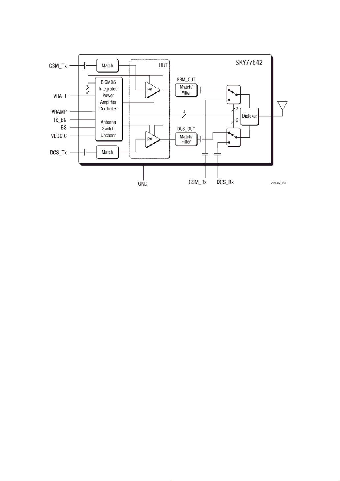
3.2 Power Amplifier Module (SKY77542)
Figure.3-2-1 SKY77542 FUNCTIONAL BLOCK DIAGRAM
The SKY77542 is a transmit and receive front-end module (FEM) with Integrated Power
Amplifier Control (iPAC.) for dual-band cellular handsets comprising GSM900 and DCS1800
operation.Designed in a low profile, compact form factor, the SKY77542 offers a complete Transmit
VCO-to- Antenna and Antenna-to-Receive SAW filter solution. The FEM also supports Class 12
General Packet Radio Service (GPRS) multi-slot operation.
The module consists of a GSM900 PA block and a DCS1800 PA block, impedance-matching
circuitry for 50 Ω input and output impedances, Tx harmonics filtering, high linearity and low
insertion loss PHEMT RF switches, diplexer and a Power Amplifier Control (PAC) block with
internal current sense resistor. A custom BiCMOS integrated circuit provides the internal PAC
function and decoder circuitry to control the RF switches. The two Heterojunction Bipolar Transistor
(HBT) PA blocks are fabricated onto a single Gallium Arsenide (GaAs) die. One PA block supports
the GSM900 band and the other PA block supports the DCS1800 band. Both PA blocks share
common power supply pads to distribute current. The output of each PA block and the outputs to
the two receive pads are connected to the antenna pad through PHEMT RF switches and a
diplexer. The GaAs die, PHEMT die, Silicon (Si) die and passive components are mounted on a
multi-layer laminate substrate. The assembly is encapsulated with plastic overmold.
Band selection and control of transmit and receive modes are performed using two external
control pads. Refer to the functional block diagram in Figure 3-2-1 below. The band select pad (BS)
selects between GSM and DCS modes of operation. The transmit enable (Tx_EN) pad controls
receive or transmit mode of the respective RF switch (Tx = logic 1). Proper timing between transmit
enable (Tx_EN) and Analog Power Control (VRAMP) allows for high isolation between the antenna
and Tx-VCO while the VCO is being tuned prior to the transmit burst.
The SKY77542 is compatible with logic levels from 1.2 V to VCC for BS and Tx_EN pads,
depending on the level applied to the VLOGIC pad. This feature provides additional flexibility for
the designer in the selection of FEM interface control logic.
22
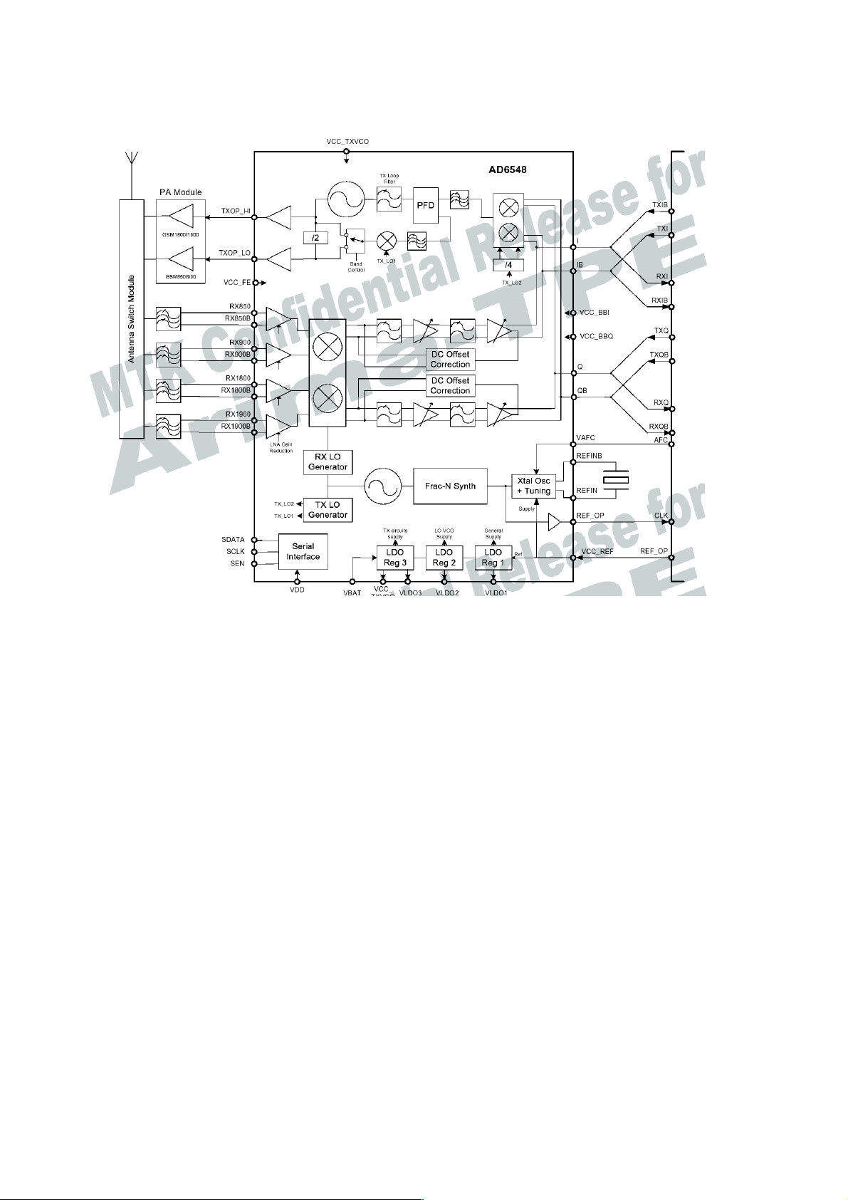
3.3 Transceiver Module (AD6548)
Figure.3-3-1 AD6548 FUNCTIONAL BLOCK DIAGRAM
3.3.1 General Descriptions
The AD6548/9 provides a highly integrated direct conversion radio solution that combines, on a
single chip, all radio and power management functions necessary to build the most compact GSM
radio solution possible. The only external components required for a complete radio design are the
Rx SAWs, PA, Switchplexer and a few passives enabling an extremely small
cost effective GSM Radio solution.
The AD6548/9 uses the industry proven direct conversion receiver architecture of the OthelloTM
family. For Quad band applications the front end features four fully integrated programmable gain
differential LNAs. The RF is then downconverted by quadrature mixers and then fed to the
baseband programmable-gain amplifiers and active filters for channel selection. The Receiver
output pins can be directly connected to the baseband analog processor. The Receive path
features automatic calibration and tracking to remove DC offsets.
The transmitter features a translation-loop architecture for directly modulating baseband signals
onto the integrated TX VCO. The translation-loop modulator and TX VCO are extremely low noise
removing the need for external SAW filters prior to the PA.
The AD6548/9 uses a single integrated LO VCO for both the receive and the transmit circuits.
The synthesizer lock times are optimized for GPRS applications up to and including class 12.
To dramatically reduce the BOM both TX Translational loop and main PLL Loop Filters are fully
23

integrated into the device.
AD6548 incorporates a complete reference crystal calibration system. This allows the external
VCTCXO to be replaced with a low cost crystal. No other external components are required. The
AD6549 uses the traditional VCTCXO reference source.
The AD6548/9 also contains on-chip low dropout voltage regulators (LDOs) to deliver regulated
supply voltages to the functions on chip, with a battery input voltage of between 2.9V and 5.5V.
Comprehensive power down options are included to minimize power consumption in normal use.
A standard 3 wire serial interface is used to program the IC. The interface features low-voltage
digital interface buffers compatible with logic levels from 1.6V to 3.0V.
The AD6548/9 is packaged in a 5mm × 5mm , 32-lead LFCSP package.
ORDERING GUIDE Model TemperatureRange Package
AD6548BCPZ
-20°C to +85°C
LFCSP-32
AD6549BCPZ -20°C to +85°C LFCSP-32
3.3.2 Features
Fully Integrated GSM Transceiver including
Direct Conversion Receiver
4 Differential LNAs
Integrated Active RX Channel Select Filters
Programmable Gain Baseband Amplifiers
Translation Loop Direct VCO Modulator
Integrated TX VCO and tank
External TX filters eliminated
Integrated Loop filter components
High performance multi band PLL system
Fast Fractional-N Synthesizer
Integrated Local Oscillator VCO
Fully Integrated Loop filters
Crystal Reference Oscillator & Tuning System (AD6548)
Power Management
Integrated LDOs allow direct battery supply connection
Small footprint
32-Lead 5 X 5 mm Chipscale Package
APPLICATIONS
Dual, Triple and Quad Band Radios
- GSM850, E-GSM 900, DCS1800 and PCS1900
- GPRS to Class 12- EDGE RX
24
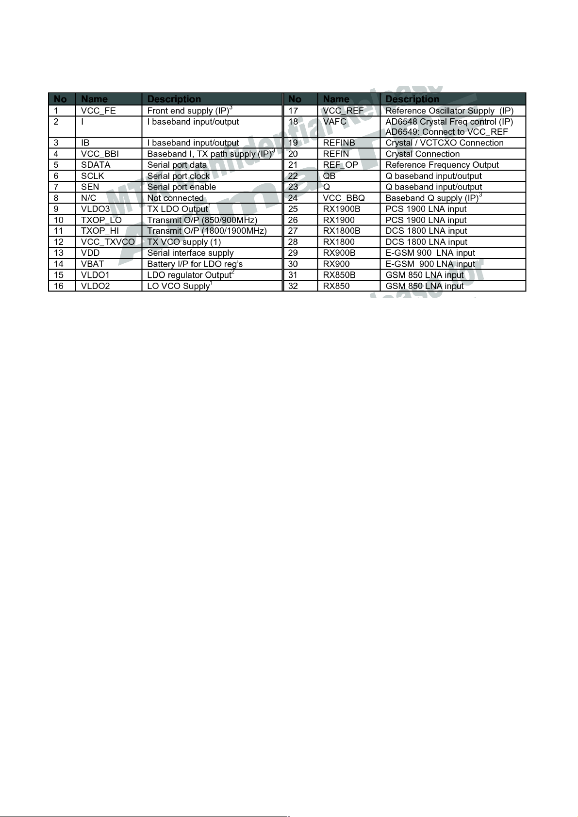
3.3.3 Pin Descriptions
25
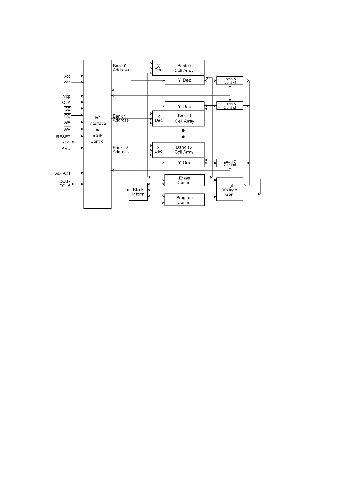
3.4 Memory Module (K5L6443ABM-AD11)
Figure.3-4-1 K5L6443ABM-AD11 FUNCTIONAL BLOCK DIAGRAM
GENERAL DESCRIPTION
The K5L6433ABM is a MultiChip Package Memory which combines 64Mbit NOR Flash
Memory and 32M bit UtRAM2.
The 64Mb NOR Flash featuring single 1.8V power supply is a 64Mbit Synchronous Burst Multi
Bank Flash Memory organized as 4Mx16. The memory architecture of the device is designed to
divide its memory arrays into 135 blocks with independent hardware protection. This block
architecture provides highly flexible erase and program capability. The 64Mb NOR Flash consists
of sixteen banks. This device is capable of reading data from one bank while programming or
erasing in the other bank. Regarding read access time, the device provides an 14.5ns burst access
time and an 70ns initial access time at 54MHz. At 66MHz, the device provides an 11ns burst
access time and 70ns initial access time. At 83MHz, the device provides an 9ns burst access time
and 70ns initial access time. At 108MHz, the device provides an 7ns burst access time and 70ns
initial access time. The device performs a program operation in units of 16 bits (Word) and an
erase operation in units of a block. Single or multiple blocks can be erased. The block erase
operation is completed within typically 0.7sec. The device requires 15mA as program/erase current
in the extended temperature ranges.
SAMSUNG’s UtRAM products are designed to meet the request from the customers who want to
cope with the fast growing mobile applications that need high-speed random access memory.
UtRAM is the solution for the mobile market with its low cost, high density and high performance
feature. device is fabricated by SAMSUNG¢s advanced CMOS technology using one transistor
memory cell. The device supports the traditional SRAM like asynchronous operation
(asynchronous page read and asynchronous write), the NOR flash like synchronous operation
(synchronous burst read and asynchronous write) and the fully synchronous operation
(synchronous burst read and synchronous burst write). These operation modes are defined
through the Confifuration Register Setting. It supports the special features for the standby power
saving. Those are the PAR(Partial Array Refresh) mode, DPD(Deep Power Down) mode and
26

internal TCSR(Temperature Compensated Self Refresh). It also supports variable and fixed
latency, driver strength settings, Burst sequence (wrap or No-wrap) options and a device ID
register (DIDR).
The K5L6433ABM is suitable for use in data memory of mobile communication system to
reduce not only mount area but also power consumption.
This device is available in 88-ball FBGA Type.
Features
<Common>
‧ Operating Temperature : -25°C ~ 85°C
‧ Package : 88-ball FBGA Type - 8mm x 10mm x 1.2mmt, 0.8mm pitch
<NOR Flash>
‧ This device has the Sync MRS option
( Extended Configuration Register )
‧ Single Voltage, 1.7V to 1.95V for Read and Write operations
‧ Organization
- 4,194,304 x 16 bit (Word Mode Only)
‧ Read While Program/Erase Operation
‧ Multiple Bank Architecture
- 16 Banks (4Mb Partition)
‧ OTP Block : Extra 256word block
‧ Read Access Time (@ CL=30pF)
- Asynchronous Random Access Time : 70ns
- Synchronous Random Access Time : 70ns
- Burst Access Time :7ns (108Mhz)
‧ Page Mode Operation
8-Words Page access allows fast asychronous read Page Read Access Time : 20ns
‧ Burst Length :
- Continuous Linear Burst
- Linear Burst : 8-word & 16-word with Wrap
‧ Block Architecture
- Eight 4Kword blocks and one hundred twenty seven 32Kword blocks
- Bank 0 contains eight 4 Kword blocks and seven 32Kword blocks
- Bank 1~Bank 15 contain one hundred twenty 32Kword blocks
‧ Reduce program time using the VPP
‧ Support Single & Quad word accelerate program
‧ Power Consumption (Typical value, CL=30pF)
- Async/Sync burst Access Current : 24mA
- Program/Erase Current : 15mA
- Read While Program/Erase Current : 40mA
- Standby Mode/Auto Sleep Mode :15uA
‧ Block Protection/Unprotection
27

- Using the software command sequence
- Last two boot blocks are protected by WP=VIL
- All blocks are protected by VPP=VIL
‧ Handshaking Feature
- Provides host system with minimum latency by monitoring RDY
‧ Erase Suspend/Resume
‧ Program Suspend/Resume
‧ Unlock Bypass Program/Erase
‧ Hardware Reset (RESET)
‧ Data Polling and Toggle Bits
- Provides a software method of detecting the status of program
or erase completion
‧ Endurance : 100,000 Program/Erase Cycles
‧ Support Common Flash Memory Interface
‧ Low Vcc Write Inhibit
<UtRAM2>
• Process technology: CMOS
• Organization: 2M x 16 bit
• Power supply voltage: 1.7V~1.95V
• Three state outputs
• Supports Configuration Register Set
- CRE pin set up
- Software set up
• Supports power saving modes
- PAR (Partial Array Refresh)
- DPD (Deep Power Down)
- Internal TCSR (Temperature Compensated Self Refresh)
• Supports driver strength optimization
• Support 2 operation modes
- Asynchronous mode (4-Page)
- Synchronous mode
• Random access time:70ns
• Page access time:20ns
• Synchronous burst operation
- Max. clock frequency : 104MHz
- Fixed and Variable read latency
- 4 / 8 / 16 / 32 and Continuous burst
- Wrap / No-wrap
- Latency : 3(Variable) @ 104MHz
- Burst stop
- Burst read suspend
- Burst write data masking
28

Pin DESCRIPTION
29
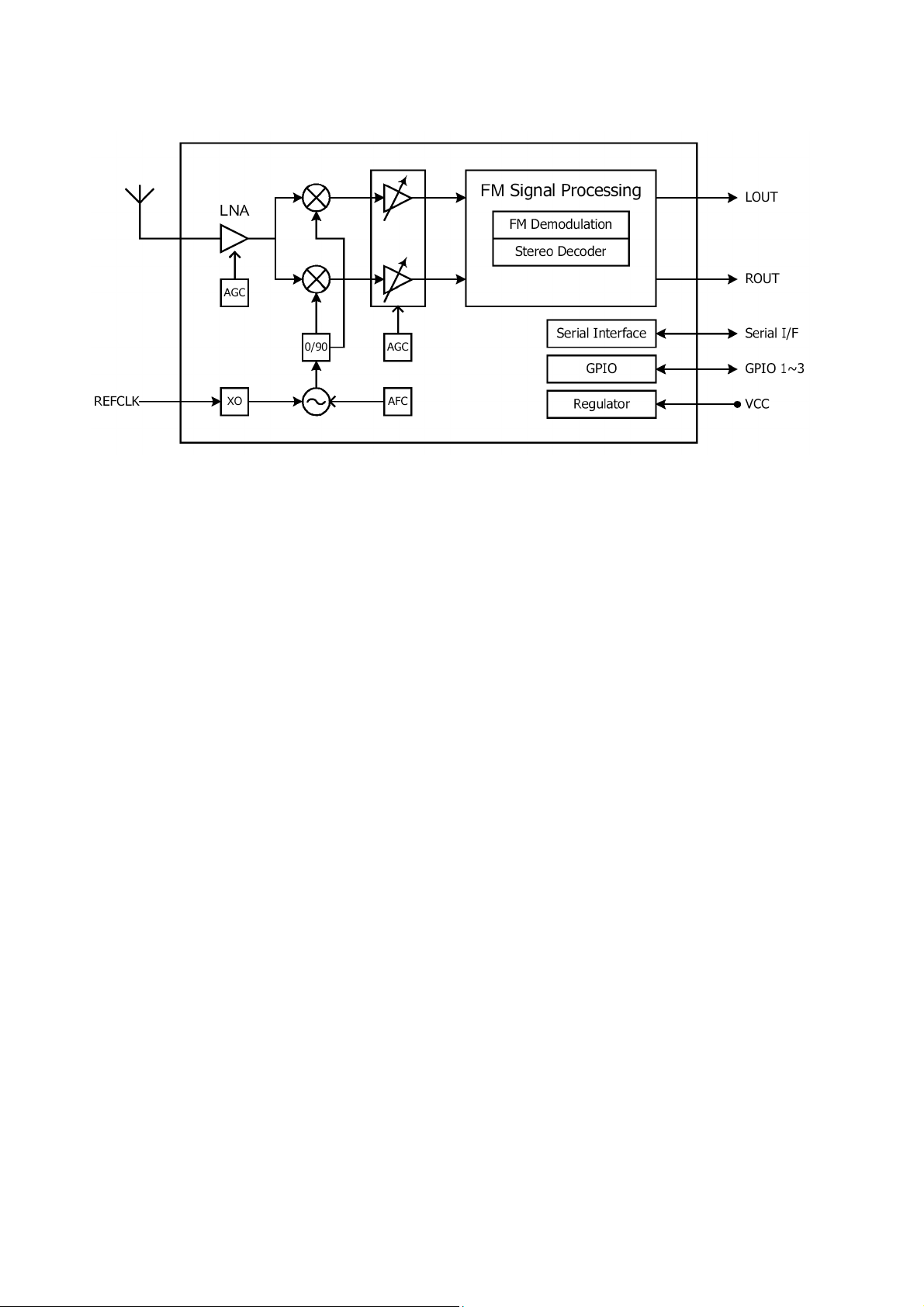
3.5 FM Radio Module (AR1200/1210)
AR1200 /AR1210 is a highly integrated single chip stereo FM radio receiver for all kinds of
applications. AR1200 /AR1210 supports worldwide FM bands from 76 to 108MHz. It integrates
LNA, Mixer, Oscillator and LDO regulator to minimize the external BOM cost.
The built-in FM signal processing unit with noise reduction mechanism provides optimum
sound quality. A simple 2-wire/3-wire interface allows easy control from the host. For
AR1200,Radio Data System(RDS) and Radio Broadcast Data System(RBDS) demodulator and
decoder are also supported.
AR1200 and AR1210 are pin-to-pin compatible and are the same in all FM radio receiver
functions, specs and packages except the RDS/RBDS function. AR1200 supports RDS/ RBDS
receiver function, while AR1210 do not.
Figure. 3-5-1
AR1200/1210
FM Receiver Block Diagram
30
 Loading...