

Page 1

787LE Service Manual
1. PRECAUTION AND NOTICES------------------------------------------------------------------------------------- 1
1.1. SAFETY PRECAUTIONS ----------------------------------------------------------------------------------------1
1.2. PRODUCT SAFETY NOTICE----------------------------------------------------------------------------------- 1
1.3. SERVICE NOTES-------------------------------------------------------------------------------------------------- 1
2. SERVICE TOOL & EQUIPMENT REQUIRED----------------------------------------------------------2
3. SPECIFICATIONS----------------------------------------------------------------------------------------------------- 2~3
PRODUCT SPECIFICATIONS
3.1.
FACTORY SUPPORTING MODES
3.2.
3.3. D-SUB CONNECTOR -------------------------------------------------------------------------------------------- 3
4. EXPLODED VIEW AND PARTS LIST --------------------------------------------------------------------------- 4~5
4.1. EXPLODED VIEW------------------------------------------------------------------------------------------------ 4
4.2. EXPLODED VIEW PARTS LIST-------------------------------------------------------------------------------- 5
5. BLOCK DIAGRAM---------------------------------------------------------------------------------------------------- 6
6. SCHEMATIC DIAGRAM -------------------------------------------------------------------------------------------- 7~13
6.1. ADE------------------------------------------------------------------------------------------------------------------ 7
6.2. POWER ------------------------------------------------------------------------------------------------------------- 8
6.3. INPUT INTERFACE ----------------------------------------------------------------------------------------------9
6.4. OUTPUT INTERFACE -------------------------------------------------------------------------------------------10
6.5. MICRO CONTROLLER ------------------------------------------------------------------------------------------ 11
6.6. POWER PCB ------------------------------------------------------------------------------------------------------- 12
6.7. INVERTER---------------------------------------------------------------------------------------------------------- 13
7. WORKING THEOREM----------------------------------------------------------------------------------------------- 14~19
8. WIRING DIAGRAM--------------------------------------------------------------------------------------------------- 20
9. PCB LAYOUT----------------------------------------------------------------------------------------------------------- 21~26
9.1. MAIN PCB TOP VIEW ------------------------------------------------------------------------------------------- 21
9.2. MAIN PCB BOTTOM VIEW------------------------------------------------------------------------------------- 22
9.3. CON PCB TOP VIEW --------------------------------------------------------------------------------------------23
9.4. CON PCB BOTTOM VIEW --------------------------------------------------------------------------------------24
9.5. POWER PCB TOP VIEW ----------------------------------------------------------------------------------------25
9.6. POWER PCB BOTTOM VIEW---------------------------------------------------------------------------------- 26
10. TROUBLE SHOOTING FLOW CHART ------------------------------------------------------------------------- 27~30
10.1. NO POWER -------------------------------------------------------------------------------------------------------- 27
10.2. MCU NO FUNCTION --------------------------------------------------------------------------------------------28
10.3. NO DISPLAY------------------------------------------------------------------------------------------------------- 29
10.4. LOSE COLOR------------------------------------------------------------------------------------------------------ 30
11. ADJUSTMENT----------------------------------------------------------------------------------------------------------31~32
11.1. ADJUSTMENT CONDITIONS AND PRECAUTIONS-------------------------------------------------------31
11.2. MAIN ADJUSTMENTS------------------------------------------------------------------------------------------- 31
11.3. ALIGNMENT PROCEDURES----------------------------------------------------------------------------------- 31
12. ELECTRICAL PARTS LIST ---------------------------------------------------------------------------------------- 33~41
TABLE OF CONTENTS
PAGE
------------------------------------------------------------------------------ 2
------------------------------------------------------------------------ 3
8/25/2003
Page 2

787LE Service Manual
1. PRECAUTION AND NOTICES
1.1. SAFETY PRECAUTIONS
This monitor is manufactured and tested on a ground principle that a user's safety comes first.
However, improper use or installation may cause damage to the monitor as well as to the user.
Carefully go over the following WARNINGS before installing and keep this guide handy.
WARNINGS:
This monitor should be operated only at the correct power sources indicated on the label on
u
the rear end of the monitor. If you're unsure of the power supply in your residence, consult
your local dealer or power company.
Use only the special power adapter that comes with this monitor for power input.
u
Do not try to repair the monitor your self as it contains no user-serviceable parts. This
u
monitor should only be repaired by a qualified technician.
Do not remove the monitor cabinet. There is high-voltage parts inside that may cause
u
electric shock to human bodies, even when the power cord is unplugged.
Stop using the monitor if the cabinet is damaged. Have it checked by a service technacian.
u
Put your monitor only in a clean, dry environment. If it gets wet, unplug the power cable
u
immediately and consult your service technician.
Always unplug the monitor before cleaning it. Clean the cabinet with a clean, dry cloth.
u
Apply non-ammonia based cleaner onto the cloth, not directly onto the glass screen.
Keep the monitor away from magnetic objects, motors, TV sets, and transformer.
u
Do not place heavy objects on the monitor or power cord.
u
1.2. PRODUCT SAFETY NOTICE
Many electrical and mechanical parts in this chassis have special safety visual inspections and
the protection afforded by them cannot necessarily be obtained by using replacement
components rated for higher voltages, wattage, etc. Before replacing any of these components
read the parts list in this manual carefully. The use of substitute replacement parts which do not
have the same safety characteristics as specified in the parts list may create shock, fire, or other
hazards.
1.3. SERVICE NOTES
1. When replacing parts or circuit boards, clamp the lead wires around terminals before
soldering.
2. When replacing a high wattage resistor (more than 1W of metal oxide film resistor) in
circuit board, keep the resistor about 5mm away from circuit board.
3. Keep wires away from high voltage, high temperature components and sharp edges.
4. Keep wires in their original position so as to reduce interference.
5. Usage of this product please refer to also user's manual.
-1-
8/25/2003
Page 3

787LE Service Manual
2. SERVICE TOOL & EQUIPMENT REQUIRED
1. SIGNAL GEN.
2. MULTIMETER
3. OSCILLOSCOPE
4. SCREW DRIVER
5. IRON
6. ABSORBER
7. SOLDER
8. DUMMY LOAD (5ohm/200W)
3. SPECIFICATIONS
3.1. PRODUCT SPECIFICATIONS
LCD Panel 17.0" TFT
Power Management Energy Star compliant VESA
DPMS compatible
< 2W
Displayable Resolution SXGA 1280× 1024 (max.)
Pixel Dimension 0.264(H)× 0.264(V)mm
LCD Display Color 16.2M Color Max. (6bit+2FRC)
Viewing Angle CR≧10
Horizontal: -70°+70°
Vertical: -65°+65°
Tilt +90°, -5°
Contrast Ratio 400 : 1 (typ.)
Brightness 200 cd/ m2 (min.)
260 cd/m2 (typ.)
Response Time Tr: 9 ms Tf: 16ms
Active Display Area 339.5mm(H)× 272mm(V)
Temperature Operating: 0°C ~ +40°C
Storage: -20°C ~ +60°C
Compliance UL 1950, C-UL, EN60950, FCC-B, CE MARK,
TÜV/GS, TCO99, CB.
Power Input Voltage: 100~240 Vac
Consumption: 45 Watts (Max.)
-2-
8/25/2003
Page 4
787LE Service Manual
3.2. FACTORY SUPPORTING MODES
There are totally 35 timings mode that can be saved in memory by FIFO architecture.
This monitor can support VGA up to SXGA resolution.
There are some resolution example listed in lookup timing table.
Lookup timing table: 1.VGA 720× 400 (70Hz) mode
2.VGA 640× 480 (60Hz) mode
3.VESA 640× 480 (72Hz) mode
4.VESA 640× 480 (75Hz) mode
5.VESA 800× 600 (56Hz) mode
6.VESA 800× 600 (60Hz) mode
7.VESA 800× 600 (72Hz) mode
8.VESA 800× 600 (75Hz) mode
9.VESA 1024× 768 (60Hz) mode
10.VESA 1024× 768 (70Hz) mode
11.VESA 1024× 768 (75Hz) mode
12.VESA 1280× 1024 (60Hz) mode
13.VESA 1280× 1024 (75Hz) mode
14.VESA 1152× 864 (75Hz) mode
15.MAC 640× 480 (67Hz) mode
16.MAC 832× 624 (74.5Hz) mode
17.MAC 1152× 870 (75Hz) mode
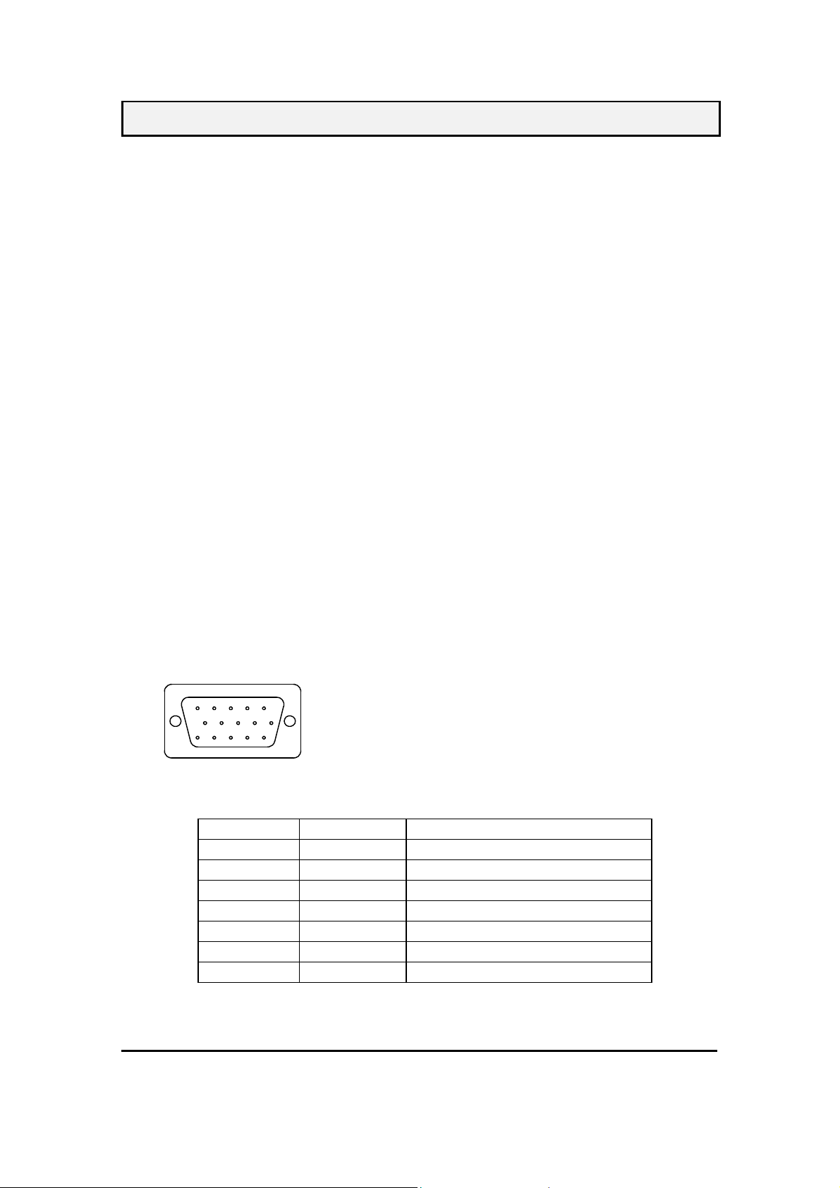
3.3. D-SUB CONNECTOR
D-SUB 15 PIN CONNECTOR
1 2 3 4 5
6 7 8 9 10
11 12 13 14 15
SIGNAL LEVEL
CONNECTOR SIGNAL DESCRIPTION
R RED 0.7vp-p(VIDEO)
G GREEN 0.7vp-p(VIDEO)
B BLUE 0.7vp-p(VIDEO)
H H/SYNC TTL positive or negative
V V/SYNC TTL positive or negative
SDA DDC1/2B TTL
SCL DDC1/2B TTL
1.R 6.GND 11.GND
2.G 7.GND 12.SDA
3.B 8.GND 13.H.SYNC
4.GND 9. +5V 14.V.SYNC
5.GND 10.GND 15.SCL
-3-
8/25/2003
Page 5
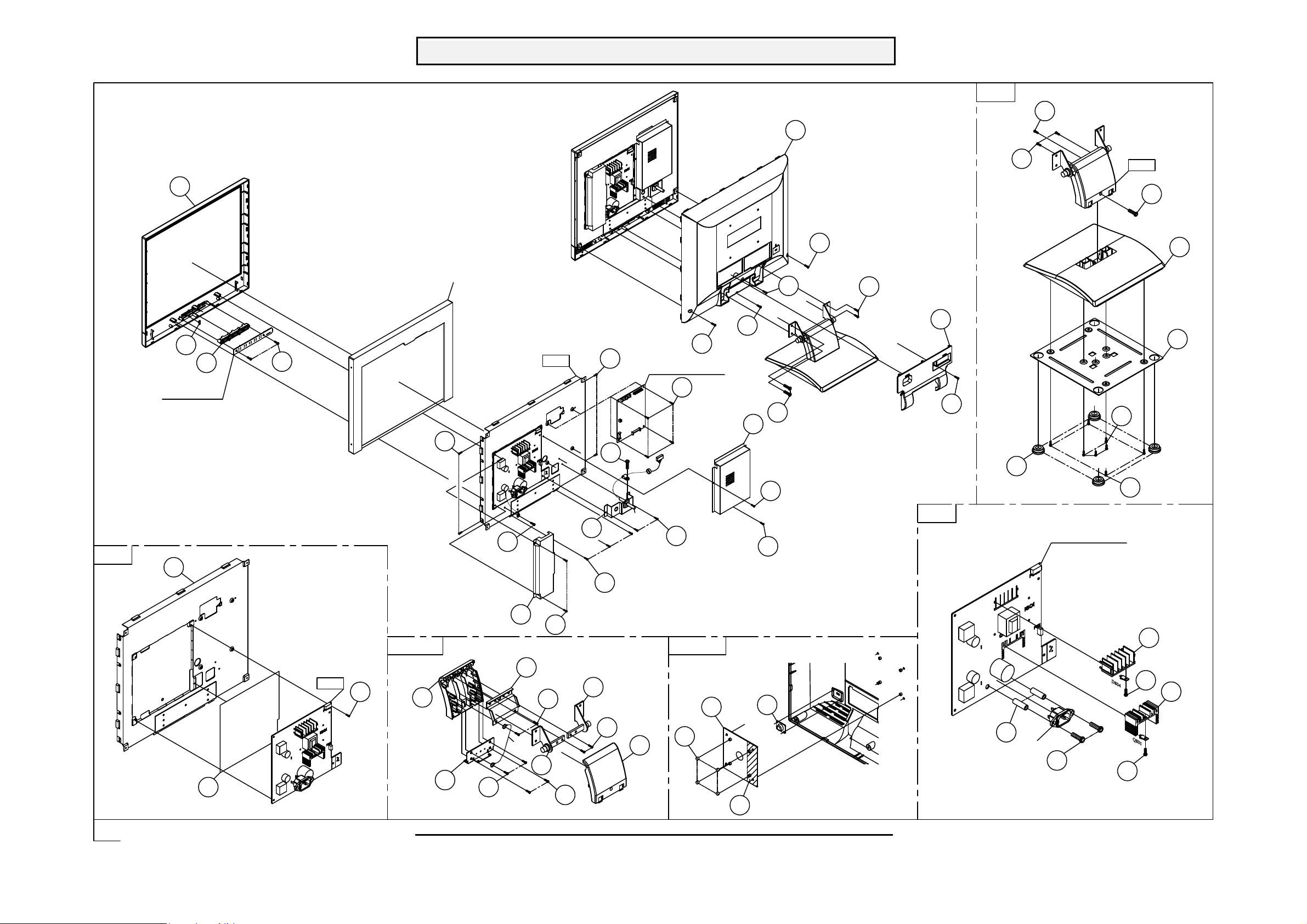
FIG.1
4.1. Exploded View
787LE Service Manual
5B11
2C01
1F01
1F02
1F03
KEYPAD PCB ASS'Y
1F12
X2
1F04
V901
X2
FIG.4
1F04
1F23
X2
1F29
MAIN PCB ASS'Y
X4
1F14
TO: MAIN PCB
P104
1F28
1F18
1F25
1F26
X2
1F29
1F25
X2
2C02
1F30
5B10 X2
5B15
X4
5B14
FIG.3
5B16
5B01
5B12
X4
FIG.4
1F05
1F08
FIG.2
1F15
FIG.3
5B02
5B07
5B08
1F24
X2
1F19
P983
5B03
5B08
5B05
1F17
X2
5B06
X2
X2
1F07
5B04
1F10
5B10
X3
X2
P961
5B09
X2
1F17
NOTE.1
2C05
X4
2C03
2C04
1F20
1F20
2C06
FIG.2
9R01
X2
POWER PCB ASS'Y
P951
9S01
X2
5B13
9S03
X4
9H02
9S02
9H03
-4-
8/25/2003
Page 6
787LE Service Manual
4.2. EXPLODED VIEW PARTS LIST
Ref. No. Source Part No. DESCRIPTION SPECIFICATION Q‘TY REMARK
1F01 2024262953 FRONT BEZEL LG ABS+PC PS-7604B MT11010 1
1F02 2053753001 LED INDIC.-PWR JT178L/LEP PMMA 94HB 1
1F03 2044262202 FUNCTION KEY JT178L ABS 94V0 PS-7604B 1
1F04 2082730062 SCREW,BND+ M3X6(BND+) 4
1F05 2071966800 METAL FITTG JT178L/SECC 0.8MM PANEL-178K77 1
1F07 2071966200 METAL FITTG JT178K77 SECC T=1.0MM(I/0) 1
1F08 2072454600 INSULATOR MYLAR(168*168T=0.5)MM(94V0) 1
1F10 2084740102 SCREW,BND T+ M4X10(BND T+) 3
1F12 2084730082 SCREW,BND T+ M3X8(BND T+) 2
1F14 2082630062 SCREW M3X6 P=0.5 4
1F15 2082630062 SCREW M3X6 P=0.5 1
1F17 2082630062 SCREW M3X6 P=0.5 4
1F18 2071666100 SHIELD PLATE JT178K77 SPTE T=0.3MM(MAIN) 1
1F19 2071667500 SHIELD PLATE JT178L/SPTE T:0.3MM(INVERTER) 1
1F20 2082630062 SCREW M3X6 P=0.5 2
1F23 2081430082 SCREW,(WASH) M3X8 P=0.5(TOOTH,WASHER) 1
1F24 2085740062 SCREW,B OTW+ B,OTW+,M4x6 1
1F25 2087340086 SCREW,B SPW+ M4X8 B SPW+ ö3.96 NYLON 4
1F26 2082740082 SCREW,BND+ M4X8(BND+) 1
1F28 2084740102 SCREW,BND T+ M4X10(BND T+) 1
1F29 2082630064 SCREW M3X6 P=0.6 BLACK 2
1F30 2082630064 SCREW M3X6 P=0.6 BLACK 1
2C01 2022259707 CABI BACK 787LE/ABS+PC BACK C LG LOGO 1
2C02 2027257503 DUST COVER JT178L/ABS+PC BLACK C 1
2C03 2071863900 BRACKET,FIX JT178L/SECC 1.0T KEWSINGTON 1
2C04 2072457100 INSULATOR PC BLACK 94V0 T=0.5 1
2C05 2072455300 INSULATOR SILICON RUBBER ö6.5Xö9.0 4
2C06 2071958300 METAL FITTG VE170 KENSINGTON 1
5B01 2028255202 STAND JT178L ABS 94HB BLACK C 1
5B02 2027255802 DUST COVER JT178L ABS 94HB BLACK C 1
5B03 2071962700 METAL FITTG JT178L SECC 1.5T HINGE(UP) 1
5B04 2106655100 HINGE JT178L(L) 0~90' 1
5B05 2106655200 HINGE JT178L(R) 0~90' 1
5B06 2084740082 SCREW,BND T+ M4X8(BND T+) 2
5B07 2071962800 METAL FITTG JT178L SECC 1.5T H1NGE (DOWN) 1
5B08 2084740082 SCREW,BND T+ M4X8(BND T+) 4
5B09 2027255902 DUST COVER JT178L/ABS 94HB BLACK C 1
5B10 2085740122 SCREW,B OTW+ SCREW B OTW+ M4X12 4
5B11 2084740102 SCREW,BND T+ M4X10(BND T+) 1
5B12 2071966700 METAL FITTG JT178L SECC 1.5T (STAND) 1
5B13 2084740082 SCREW,BND T+ M4X8(BND T+) 4
5B14 2082740122 SCREW,BND+ M4X12 (BND+) 4
5B15 2039802303 FOOT PAD VA520 CR420xö16.5x5.8 BLACK 4
5B16 2082630062 SCREW M3X6 P=0.5 1
9H02 2072259700 HEAT SINK JT178K77 44WX27LX20H 1
9H03 2072259600 HEAT SINK JT178K77 45WX20LX20H 1
9R01 2063252000 SPACER SUPPORT NYLON 66 94V2 15.87*06.6*42.5 2
9S01 2083730102 SCREW,BND T+ SCREW BND T+ 2
9S02 2084730082 SCREW,BND T+ M3X8(BND T+) 1
9S03 2084730082 SCREW,BND T+ M3X8(BND T+) 1
-5-
9/24/2003
Page 7
5. BLOCK DIAGRAM
787LE Service Manual
AC INPUT
100V ~ 220V
SYNC
I105
SW power supply
12V
I801
INVERTER
I901
P102
Q101,Q104
R.G.B INPUT
DC-DC
I804
PANEL
DISPLAY
LVDS
I106,I107
SCALAR
I101
MCU
I108,DDC
5V
VLCD
Q102
3.3V
I103
1.8V
I104
5V MCU
Q107,Q108
H,V SYNC
VGA INPUT
P104
SCL,SDA
VGA 5V
EEPROM
I109
-6-
OSC
X101
8/25/2003
Page 8
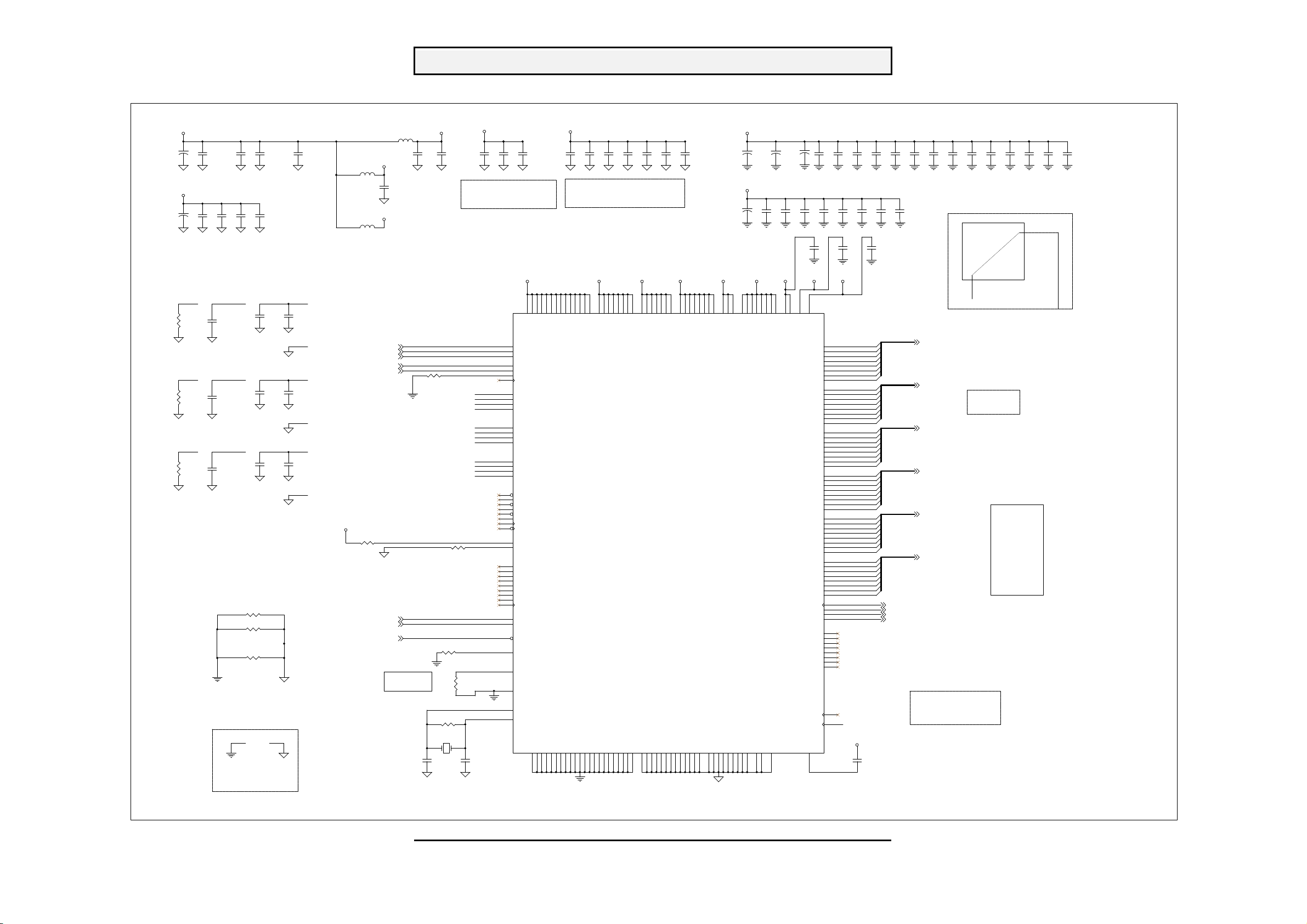
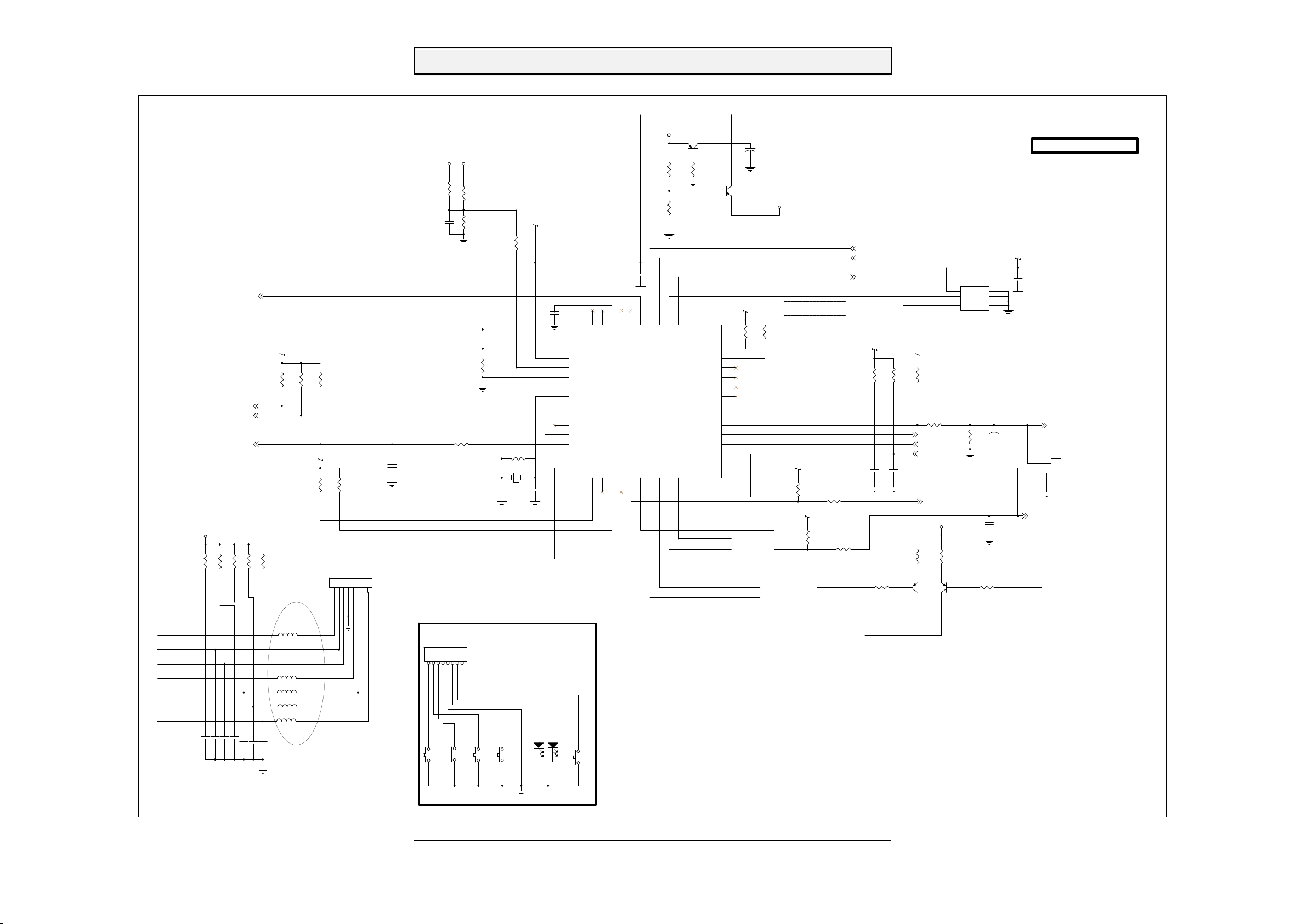
6. Schematic Diagrams
6.1. ADE
787LE Service Manual
AVDD_1.8
C101
47uF/16V
C148
47uF/16V
C102
0.1uF
AVDD_3.3
C150
C149
0.1uF
0.1uF
REFR
REFG
REFCR
R102
15K 1%
0603
R104
15K 1%
0603
REFB
R106
15K 1%
0603
C155
0.1uF
0603
REFCG
C158
0.1uF
0603
REFCB
C161
0.1uF
0603
INTERNAL ADC REFERENCE RESISTORS AND
DECOUPLING CAPACITORS. PLACE THESE
COMPONENTS CLOSE TO THEIR RESPECTIVE
PINS
DGND
AGND and DGND are isolated,
not completely separated
Place near PAD1
C104
0.1uF
C151
0.1uF
R201 0R 0805
R202 0R 0805
R204 0R 0805
DGND
C105
0.1uF
C152
0.1uF
REFPR
C153
0.47uF
0603
REFPG
C156
0.47uF
0603
REFPB
C159
0.47uF
0603
AGND
AGND
C154
100pF
REFMR
C157
100pF
0603
REFMG
C160
100pF
0603
REFMB
C107
0.1uF
BEAD120R
RVDD_3.3
L101
1 2
0805
L103
1 2
0805
BEAD100R
R101
NC
ADE-RESET#[6]
BEAD120R
XVDD_1.8
LVDD_1.8
AHSYNC[4]
AVSYNC[4]
ADE-SCL[6]
ADE-SDA[6]
L102
1 2
0805
C138
0.1uF
0603
INR[4]
ING[4]
INB[4]
XCLK_EN
0:xclk o/p disable
1:xclk o/p active
C162
22pF
0603
C109
0.1uF
0603
R187
0603
PVDD_1.8
C110
0.1uF
0603
0R
R108 NC
R188
0R
0603
R110
0R
0603
R111
1M0603
X101
27MHz Crystal
AVDD_1.8
C111
0.1uF
0603
PLACE CAPACITORS C111, C112,
AND C113 ON PINS 14, 38, AND 42,
RESPECTIVELY
(TMDS power supply pins)
REFR OGA1
REFCR
REFPR
REFMR
REFG
REFCG
REFPG
REFMG
REFB
REFCB
REFPB
REFMB
C163
22pF
0603
C113
C112
1nF
0.1uF
DVDD_1.8 AVDD_1.8
I101
92
INR
80
ING
68
INB
55
HSYNC
54
VSYNC
53
CSYNC
183
CLKIN
87
REFR
95
REFCR
89
REFPR
88
REFMR
75
REFG
83
REFCG
77
REFPG
76
REFMG
63
REFB
71
REFCB
65
REFPB
64
REFMB
16
RX2M
17
RX2P
20
RX1M
21
RX1P
23
RX0M
24
RX0P
27
RXCP
28
RXCM
30
REXT
36
RBIAS
7
YUV0
6
YUV1
5
YUV2
4
YUV3
3
YUV4
2
YUV5
1
YUV6
208
YUV7
8
YUVCLK
203
SCL
204
SDA
207
RESETN
184
TCON_IN
206
XCLK_EN
99
TST_SCAN
48
XTAL_IN
49
XTAL_OUT
9
DVDD18
DGND DVDD18
10 11
121
123
140
DVDD18
DVDD18
DGND
DGND
12
100
105
AVDD_3.3
C114
10nF
0603
142
164
DVDD18
DVDD18
DVDD18
DGND
DGND
DGND
112
122
C115
C116
100pF
0.1uF
PLACE CAPACITORS C114, C115, C116, C117,
C118, C119, AND C120 ON PINS 15, 19, 22, 25,
29, (31 & 32), AND 40, RESPECTIVELY
(TMDS power supply pins)
DVDD_3.3 PVDD_1.8AVDD_3.3 AVDD_3.3
166
178
180
191
193
199
201
101
111
125
134
148
158
172
DVDD18
DVDD18
DVDD18
DVDD18
DVDD18
DVDD18
DVDD18
DVDD33
DVDD33
DVDD33
DVDD33
DVDD33
DVDD33
DGND
DGND
DGND
DNGD
DGND
DGND
DGND
DGND
DGND
DGND
DGND
DGND
DGND
DGND
124
135
141
143
149
159
165
167
173
179
181
186
192
194
200
DVDD_1.8
C123
C122
C118
C119
AVDD18
AVDD18
AVDD18
0.1uF
58596970818293
AVDD18
AVDD18
C120
10nF
AVDD33
AVDD33
AVDD33
AVDD33
C117
1nF
10nF
AVDD_1.8 LVDD_1.8 XVDD_1.8
185
61737485869798
AVDD18
AVDD18
DVDD33
DVDD33
ADE3XXX
PQFP208
DGND
DGND
AGND
AGND
AGND
AGND
AGND
AGND
AGND
AGND
AGND
AGND
AGND
AGND
202
56576062666772787984909196
C121
47uF/16V
DVDD_3.3
C139
47uF/16V
143842
15192225293132
94
AVDD33
AVDD33
AVDD33
AVDD33
RVDD18
RVDD18
RVDD18
RVDD33
RGND
RGND
RGND
RGND
RGND
RGND
RGND
AGND
1318263334353739414345
RGND
47uF/16V
RVDD33
RVDD33
RVDD33
RGND
PGND
C140
0.1uF
40
RVDD33
RVDD33
RVDD33
PGND
XGND
47
47uF/16V
C141
0.1uF
44
46
PVDD18
RVDD33
51
LVDD18
PVDD18
TCON0
TCON1
TCON2
TCON3
TCON4
TCON5
TCON6
TCON7
CLKOUT
C142
0.1uF
10uF/10V
ORA0
ORA1
ORA2
ORA3
ORA4
ORA5
ORA6
ORA7
OGA0
OGA1
OGA2
OGA3
OGA4
OGA5
OGA6
OGA7
OBA0
OBA1
OBA2
OBA3
OBA4
OBA5
OBA6
OBA7
ORB0
ORB1
ORB2
ORB3
ORB4
ORB5
ORB6
ORB7
OGB0
OGB1
OGB2
OGB3
OGB4
OGB5
OGB6
OGB7
OBB0
OBB1
OBB2
OBB3
OBB4
OBB5
OBB6
OBB7
OCLK
XCLK
C232
50
XVDD18
ODE
OHS
OVS
LGND
52
C124
0.1uF
C143
0.1uF
133
132
131
130
129
128
127
126
120
119
118
117
116
115
114
113
110
109
108
107
106
104
103
102
177
176
175
174
171
170
169
168
163
162
161
160
157
156
155
154
153
152
151
150
147
146
145
144
138
136
137
139
198
197
196
195
190
189
188
187
205
182
C125
0.1uF
C144
0.1uF
C233
1uF
ORA0
ORA1
ORA2
ORA3
ORA4
ORA5
ORA6
ORA7
OGA0
OGA2
OGA3
OGA4
OGA5
OGA6
OGA7
OBA0
OBA1
OBA2
OBA3
OBA4
OBA5
OBA6
OBA7
ORB0
ORB1
ORB2
ORB3
ORB4
ORB5
ORB6
ORB7
OGB0
OGB1
OGB2
OGB3
OGB4
OGB5
OGB6
OGB7
OBB0
OBB1
OBB2
OBB3
OBB4
OBB5
OBB6
OBB7
LVDD_1.8
C126
0.1uF
C164
0.1uF
0603
C145
0.1uF
C234
1uF
C127
0.1uF
C146
0.1uF
OCLK [5]
ODE
OHS
OVS
C128
C129
0.1uF
0.1uF
C147
0.1uF
0805
ORA[7:0] [5]
OGA[7:0] [5]
OBA[7:0] [5]
ORB[7:0] [5]
OGB[7:0]
OBB[7:0] [5]
[5]
[5]
[5]
Indicate Pin# at every 5/10 pins
5 : short line
10 : long line
1,53,105 &157 should be
labeled
C131
C130
0.1uF
0.1uF
ADE3000
1 52
[5]
C133
C132
0.1uF
0.1uF
GND splitting
* Same VIA #
* Similar
length
C134
0.1uF
AGND
104
RB
GB
BB
Sync
RA
GA
BA
C135
0.1uF
DGND
C136
0.1uF
C137
0.1uF
-7-
9/24/2003
Page 9
6.2. Power
787LE Service Manual
P101
ON/OFF
1
BRIGHT
2
5V
3
4
GND
5
MUTE
6
VOLUM
7
8
[6]
ON/OFF
[6]
BRIGHT
PAD4
1
2
3
4 5
9
PAD2
1
2
3
4 5
9
8
7
6
8
7
6
MUTE 3
PAD5
1
2
3
4 5
9
PAD3
1
2
3
4 5
9
VOLUM 3
8
7
6
8
7
6
+5V
470uF/25V
DVDD_3.3
C170
L107
0.47/2W
1 2
0.47/2W
R256
L130
NC
1206
C178
0.1uF
0603
I103
RA:AMC7585-3.3ST
RB:AIC1084-33CM
R254
NC
I103
3
AIC1084
INPUT
OUTPUT
GND
1
I104 RC1117-ADJ
ADJ
VOUTVIN
SOT223
1
12V
249 1%
NC
2
23
R121
0603
L104
470uF/16V
C176
330uF/16V
Copper plate
Min : 10 x 10
mm
R120
0603
560
47uF/16V
DVDD_3.3
C177
0.1uF
C179
C165
NC
C171
1 2
DVDD_1.8
12
+
L119
BEAD60R
1206
C180
0.1uF
0603
C242
NC
AVDD_3.3
1206
L132
1 2
BEAD60R
L131
1 2
BEAD60R
1206
5V
CPT 18" USE L105 ONLY
AU 17",CMO 17",SANYO 18"
USE L106 ONLY
PAN 12V
L106
BEAD60R
1206
C174
NC
[6]
PANELPOWER
AVDD_1.8
R115
330
R119
2.2K
1Amax
NC
L105
1206
R116
330
Q102
KSB772
R113
10K
R118
R117
330
330
Q103
MMBT3904
DGND
DGND
PGND and DGND are isolated,
not completely separated
VLCD
CPT 18" R115,R116,R117,R118
USE 1.6K
-8-
9/24/2003
Page 10
6.3. Input Interface
787LE Service Manual
INPUT INTERFACE
AVDD_3.3AVDD_3.3 AVDD_3.3
R134
47
0603
R135 100
0603
P104
10
11
12
13
1
2
3
4
5
6
7
8
9
1
2
3
4
5
6
7
8
9
10
11
12
13
D120
ZD5V6
1 2
DB15-SCL
DB15-SDA
DB15-AVSYNC
DB15-AHSYNC
VGA_5V
BLUE
GREEN
RED
DDC-SCL [6]
DDC-SDA[6]
VGA_5V
D103
1N4148
D106
1N4148
D104
1N4148
1 2
D107
1N4148
1 2
R128
75
0603
D105
1N4148
1 2
D108
1N4148
1 2
R129
75
0603
R128-130
Place at
CN side
Place near CN
1 2
1 2
L120
0603 0R
1 2
L121
0603 0R
1 2
L122
0603 0R
1 2
L120,L121,L122 change to 0R
R130
75
0603
Guraded by AGND All the way
(From CN to ADE) & >= 12mil
0603
R122 100
100
R125
R127 100
C187
C188
NC
NC
0603
0603
C182 0.1uF
C183 0.1uF
C186 0.1uF
0603
C189
NC
0603
R197
0R 0603
R198
0R 0603
R1990R0603
AGND
R/G/B
INB
ING
INR
AHSYNC is important signal
First Priority with Least VIA
TOP side ONLY
DB15-AHSYNC
[2]
[2]
[2]
DB15-AVSYNC
R126
33K/NC
0603
R133
33K/NC
0603
R123
330
0603
R131
330
0603
RC-AHSYNC
C240
C184
NC
0.1uF
0603
0603
RC-AVSYNC
C190
NC
0603
AVDD_3.3
23
D119
BAT54C
1
SOT-23
L127
BEAD120R
0805
1 2
I105F
14
13 12
7
74LVC14
SO-14
I105E
14
11 10
7
74LVC14
SO-14
R124
0603
22
R132
0603
AHSYNC [2]
C185
22P
0603
C191
22P
0603
AVSYNC [2]
22
AGND
Add VIA on AGND
every 10mm
C192
47p
C193
NC
D110
NC
D114
ZD5.6V
AVDD_3.3
1 2
1 2
R139
10K
0603
D111
NC
1 2
D115
ZD5.6V
1 2
D112
NC
1 2
D116
ZD5.6V
1 2
D113
NC
1 2
D117
ZD5.6V
1 2
Analog Input (VGA)
Place near CN
R140
10K
0603
RC-AVSYNC
RC-AHSYNC
I105A
14
1 2
7
74LVC14
SO-14
I105B
14
3 4
7
74LVC14
SO-14
R137
MCU_VS
100 0603
R138
MCU_CS
100 0603
-9-
9/24/2003
Page 11
6.4. Output Interface
787LE Service Manual
ORA[7:0][2]
OGA[7:0][2]
OBA[7:0][2]
These are CRITICAL signal
NO VIA is allowed
OVS[2]
OCLK[2]
OHS[2]
ODE[2]
BRIGHTNESS[6]
BLON pin : Reset HIGH
Place Q104 if inverter is Low active
Place R180 if inverter is High active
C210
CAP/NC
0603
OBA0
OBA1
OBA2
OBA3
OBA4
OBA5
OBA6
OBA7
OCLK
OHS
ODE
OVS
ORA0
ORA1
ORA2
ORA3
ORA4
ORA5
ORA6
ORA7
OGA0
OGA1
OGA2
OGA3
OGA4
OGA5
OGA6
OGA7
1
2
3
4
1
2
3
4
R147 22
R148 22
R149 22
R151 22
R157
4.7K
0603
1
2
3
4
1
2
3
4
1
2
3
4
1
2
3
4
RP09
RP8SF
RP11
RP8SF
RP01
RP8SF
RP03
RP8SF
RP05
RP8SF
RP07
RP8SF
22R
22R
[6]
22R
22R
22R
22R
MMBT3904
BLON
3 2
8
7
6
5
8
7
6
5
0603
0603
0603
0603
0603
R251
SOT-23
1
Q104
MMBT3904
ORB[7:0][2]
OGB[7:0][2]
OBB[7:0][2]
C215
0.1uF
0603
RA0
8
RA1
7
RA2
6
RA3
5
RA4
8
RA5
7
RA6
6
RA7
5
GA0
8
GA1
7
GA2
6
GA3
5
GA4
8
GA5 GB5
7
GA6
6
GA7
5
BA0
BA1
BA2
BA3
BA4
BA5
BA6
TP12
1
FPVS
FPCLK
FPHS
FPDE
C211
CAP/NC
0603
+5V
R155
1K
0603
R156
1
Q101
2
MMBT3904
R160
NC
0603
2.2K
NC
3
0603
C212
0603
NC
0603
R159
TP13
R174
4.7K
0603
1
TP14
C213
0603
+
10uF/16V
1
C241
TP15
C214
0603
3
SOT-23
1
R252
NC
0603
+5V
R158
4.7K
0603
1
2
OBB0
OBB1
OBB2
OBB3
OBB4
OBB5
OBB6
OBB7
ORB0
ORB1
ORB2
ORB3
ORB4
ORB5
ORB6
ORB7
OGB0
OGB1
OGB2
OGB3
OGB4
OGB5
OGB6
OGB7
1
2
3
4
1
2
3
4
RP02
1
2
3
4
22R
RP8SF
RP04
1
2
3
4
22R
RP8SF
RP06
1
2
3
4
22R
RP8SF
RP08
1
2
3
4
22R
RP8SF
RP10
8
7
6
5
22R
RP8SF
RP12
8
7
6
5
22R
RP8SF
RB0
8
RB1
7
RB2
6
RB3
5
RB4
8
RB5
7
RB6
6
RB7
5
GB0
8
GB1
7
GB2
6
GB3
5
GB4
8
7
GB6
6
GB7
5
FPHS
FPVS
FPDE
DVDD_3.3
FPCLK
BB0
BB1
BB2
BB3
BB4
BB5
BB6
BB7BA7
FPHS
FPVS
FPDE
VCC_LVDS
RB6
RB7
RB0
RB1
RB2
RB3
RB4
RB5
GB6
GB7
GB0
GB1
GB2
GB3
GB4
GB5
BB6
BB7
BB0
BB1
BB2
BB3
BB4
BB5
FPCLK
0603
L123
BEAD60
1206
C202
0.1uF
C203
0.1uF
0603
RA6
RA7
RA0
RA1
RA2
RA3
RA4
RA5
GA6
GA7
GA0
GA1
GA2
GA3
GA4
GA5
BA6
BA7
BA0
BA1
BA2
BA3
BA4
BA5
50
51
52
54
55
56
10
11
12
14
16
18
15
19
20
22
23
24
25
27
28
30
31
VCC_LVDS
C194
0.1uF
0603
C204
0.1uF
0603
TXIN27
2
TXIN5
TXIN0
TXIN1
TXIN2
TXIN3
TXIN4
3
TXIN6
8
TXIN10
TXIN11
4
TXIN7
6
TXIN8
7
TXIN9
TXIN12
TXIN13
TXIN14
TXIN16
TXIN17
TXIN15
TXIN18
TXIN19
TXIN20
TXIN21
TXIN22
TXIN23
TXIN24
TXIN25
TXIN26
TXCLKIN
C195
0.1uF
0603
50
51
52
54
55
56
10
11
12
14
16
18
15
19
20
22
23
24
25
27
28
30
31
C205
0.1uF
0603
2
3
8
4
6
7
C196
0.1uF
0603
TXIN27
TXIN5
TXIN0
TXIN1
TXIN2
TXIN3
TXIN4
TXIN6
TXIN10
TXIN11
TXIN7
TXIN8
TXIN9
TXIN12
TXIN13
TXIN14
TXIN16
TXIN17
TXIN15
TXIN18
TXIN19
TXIN20
TXIN21
TXIN22
TXIN23
TXIN24
TXIN25
TXIN26
TXCLKIN
1917
VVV
I107
CS5824
TSSOP56
C197
0.1uF
0603
26
V
TXCLKOUT-
TXCLKOUT+
1917
VVV
I106
CS5824
TSSOP56
PWRDWN
TXOUT0-
TXOUT0+
TXOUT1-
TXOUT1+
TXOUT2-
TXOUT2+
TXOUT3-
TXOUT3+
LVDSVCC
LVDSGND
LVDSGND
LVDSGND
PLLVCC
PLLGND
PLLGND
GND
GND
GND
GND
GND
26
V
PWRDWN
TXOUT0-
TXOUT0+
TXOUT1-
TXOUT1+
TXOUT2-
TXOUT2+
TXOUT3-
TXOUT3+
TXCLKOUT-
TXCLKOUT+
LVDSVCC
LVDSGND
LVDSGND
LVDSGND
PLLVCC
PLLGND
PLLGND
GND
GND
GND
GND
GND
32
48
TXB1
47
46
45
42
41
38
37
40
39
44
49
43
36
34
35
33
53
29
21
13
5
LVDSPDN
TXB0
TXB2
TXB3
TXB4
TXB5
TXB6
TXB7
TXB8
TXB9
DVDD_3.3
R141
10K
0603
LVDSPDN
32
TXA0
48
TXA1
47
TXA2
46
TXA3
45
TXA4
42
TXA5
41
TXA6
38
TXA7
37
TXA8
40
TXA9
39
R142 0R
44
49
43
36
34
35
33
53
29
21
13
5
C199
0.1uF
0603
C200
10nF
0603
C198
0.1uF
0603
C201
1nF
0603
0603
L110
BEAD120R
0805
L111
BEAD120R
0805
LVDS_STBY[6]
VCC_LVDS
VCC_LVDS
VLCD
C169
0.1uF
C166
+
330uF/16V
GND
TXB0
TXB2
TXB4
TXB8
TXB6
TXA0
TXA2
GND
TXA4
TXA8
TXA6
VCC_LVDS
L112
C206
BEAD120R
0805
0.1uF
0603
VCC_LVDS
L113
C207
0.1uF
0603
C208
10nF
0603
C209
1nF
0603
BEAD120R
0805
OUTPUT INTERFACE
P105
1
2
1
2
3
4
3
4
6
5
6
7
19
16
13
11
9
30
28
17
26
23
21
CONN 15x2
5
7
9
11
13
15
17
19
21
23
25
27
29
GND
14
8
18
10
TXB3
15
12
12
14
TXB9
10
16
18
20
22
24
26
28
30
TXB7
8
TXA1
29
27
GND
24
25
TXA9
22
20
THE 6 PIN PCB MUST
CANCER DELETE
TXB1
TXB5
TXA3
TXA5
TXA7
BRIGHT [3]
ACTVE LOW
ON/0FF [3]
-10-
9/24/2003
Page 12
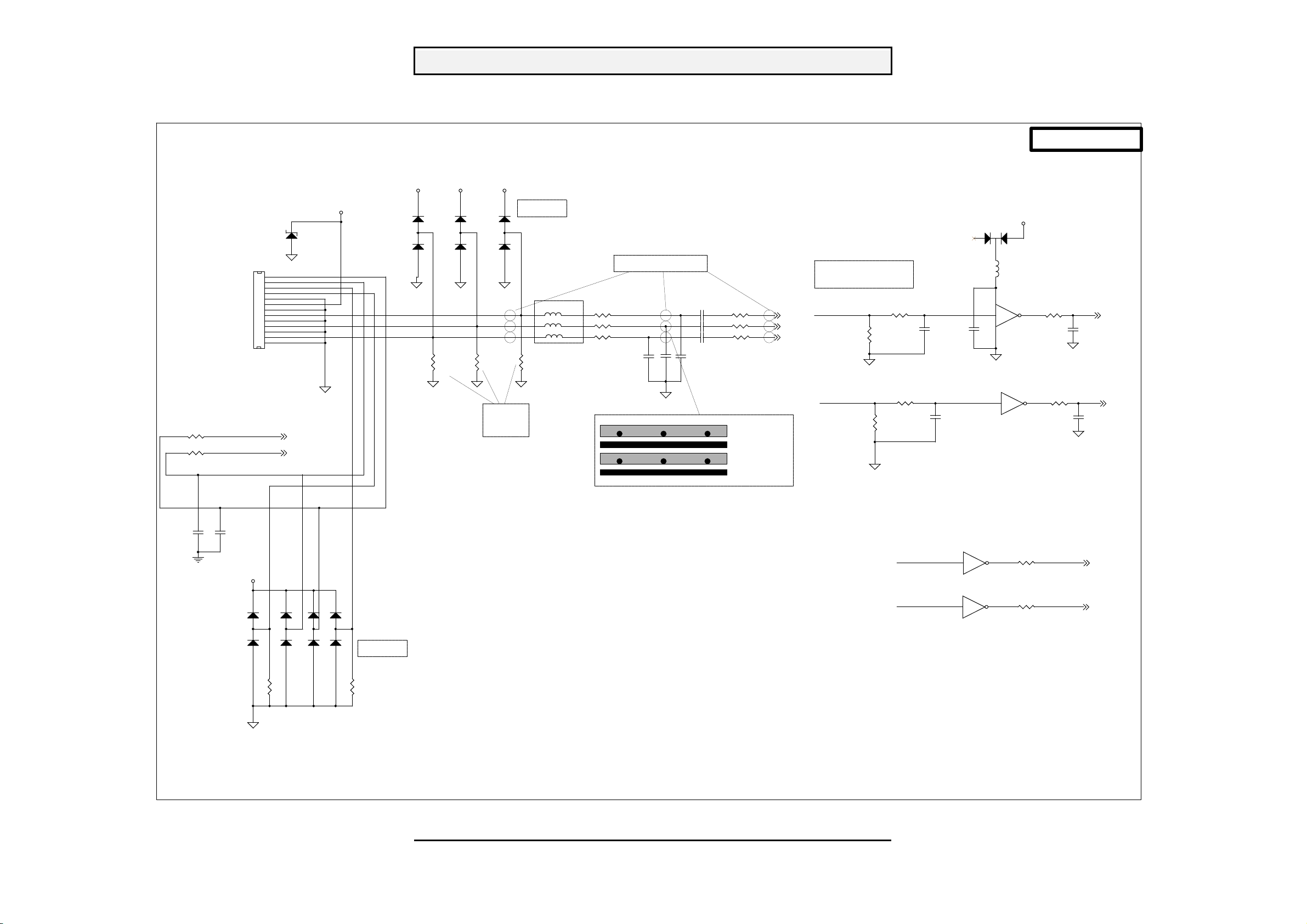
6.5. MICROCONTROLLER
[3]
PANELPOWER
R178
3.3K
0603
ADE-SDA
[2]
ADE-SCL
[2]
ADE-RESET#[2]
+5V
R194
R193
POWER
LED_ORG
LED_GRN
MENU
UP
DOWN
ENTER
OSD Control
Panel
Interface
R192
3.3K
0603
C225NC
3.3K
0603
R195
R196
3.3K
3.3K
3.3K
0603
0603
0603
L114 BEAD600R
L115 BEAD600R
L116 BEAD600R
L117 BEAD600R
L118 BEAD600R
C226NC
C228NC
C227
C229NC
C230NC
NC
C231NC
R179
3.3K
0603
R180
NC
0603
+5V_MCU
R182
3.3K
0603
I/O KEY PORT
P103 CON8
CW5
787LE Service Manual
+5V
Q107
MMBT3906
C239
/STANDBY
WP
+5V_MCU
47uF
R168
100K
0603
BRIGHTNESS
RXD
TXD
VGA 5V
Write Protect (H:protect)
R169
10K
0603
+5V_MCU
* From 7414
MCU_VS
MCU_CS
LVDS_STBY
[4]
SCL
SDA
I109
24C16
DIP8
VCC
TEST
SCL
SDA
GND
1
A0
2
A1
3
A2
4
8
7
6
5
EEPROM
+5V_MCU
R175
4.7K
0603
R176
4.7K
0603
+5V_MCU+5V_MCU
R243
NC
0603
POWER
ENTER
2.2K
0603
BRIGHTNESS
DDC-SCL
R200
VOLUME
R244
[4]
2.2K
DDC-SDA
C220
NC
R242
0603
100
0603
100
0603
R165
LED_GRN
LED_ORG
R245
NC
0603
R246
+5V_MCU
R241
NC
0603
LED-GREENLED-GREEN LED-ORANGE
10k
0603
C221
33pF
0603
Q105
MMBT3906
R185
680
0603
BLON
+5V
Backlite ON
R186
680
0603
Q106
MMBT3906
C244
NC
0603
R167
0603
MUTE
10k
+12V
R183
3.3K
0603
ADE-SDA
ADE-SCL
ADE-RESET#
C238
0.1uF
0603
C216
0.1uF
0603
R253
0603
5V
R210
1k
R161
0
NC
0603
R162
R220
1K
0603
NC
0603
22pF
R177
0603
C222
0603
1K
C219
0.1uF
0603
R181
0603
X102
12MHz Crystal
R190
100
0603
1M
+5V_MCU
C218
0.1uF
0603
C223
22pF
0603
7
RST
8
VDD
9
P6.3/AD3
10
VSS
11
X2
12
X1
13
ISDA/P3.4/T0
14
ISCL/P3.5/T1
15
STOUT/P4.2
16
P6.2/AD2/HLFHI
17
P1.0
C217
0.1uF
0603
1
2
3
4
5
6
NC
NC
VDD3
DA0/P5.0
DA2/P5.2
DA1/P5.1
44
VSYNC
43
HSYNC
I108
MTV312M44PLCC
P1.1
P3.2/INT0
P1.2
P1.3
P1.4
P1.5
P1.6
P1.7
1819202122232425262728
R212
10K
41
42
DA3/P5.3
P6.1/AD1
DA4/P5.4
P6.0/AD0
R211
1.5K
MMBT3906
40
DA5/P5.5
DA8/HLFHO
DA9/HALFV
HBLANK/P4.1
VBLANK/P4.0
DA7/HCLAMP
DA6/P5.6
P6.7/DA13
P6.6/DA12
P6.5/DA11
P6.4/DA10
HSCL/P3.0/Rxd
HSDA/P3.1/Txd
Q108
39
38
37
36
35
34
33
32
31
30
29
SCL
SDA
MENU
UP
DOWN
8
1234567
LED-ORANGE
CW3
CW6
CW7
CW1
CW2
CW4
P701
8 HEADER
DOWN
S705
1234567
1
UP
S703
S702
PWR/SW
PSM/LED
PWR/LED
KEY PAD
GREEN
S704
ORANGE
D701
S706
8
2
MICROCONTROLLER
+5V_MCU
C224
0.1uF
0603
MUTE
VOLUME
P106
1
2
3
NC
C243
10u /50V
-11-
9/24/2003
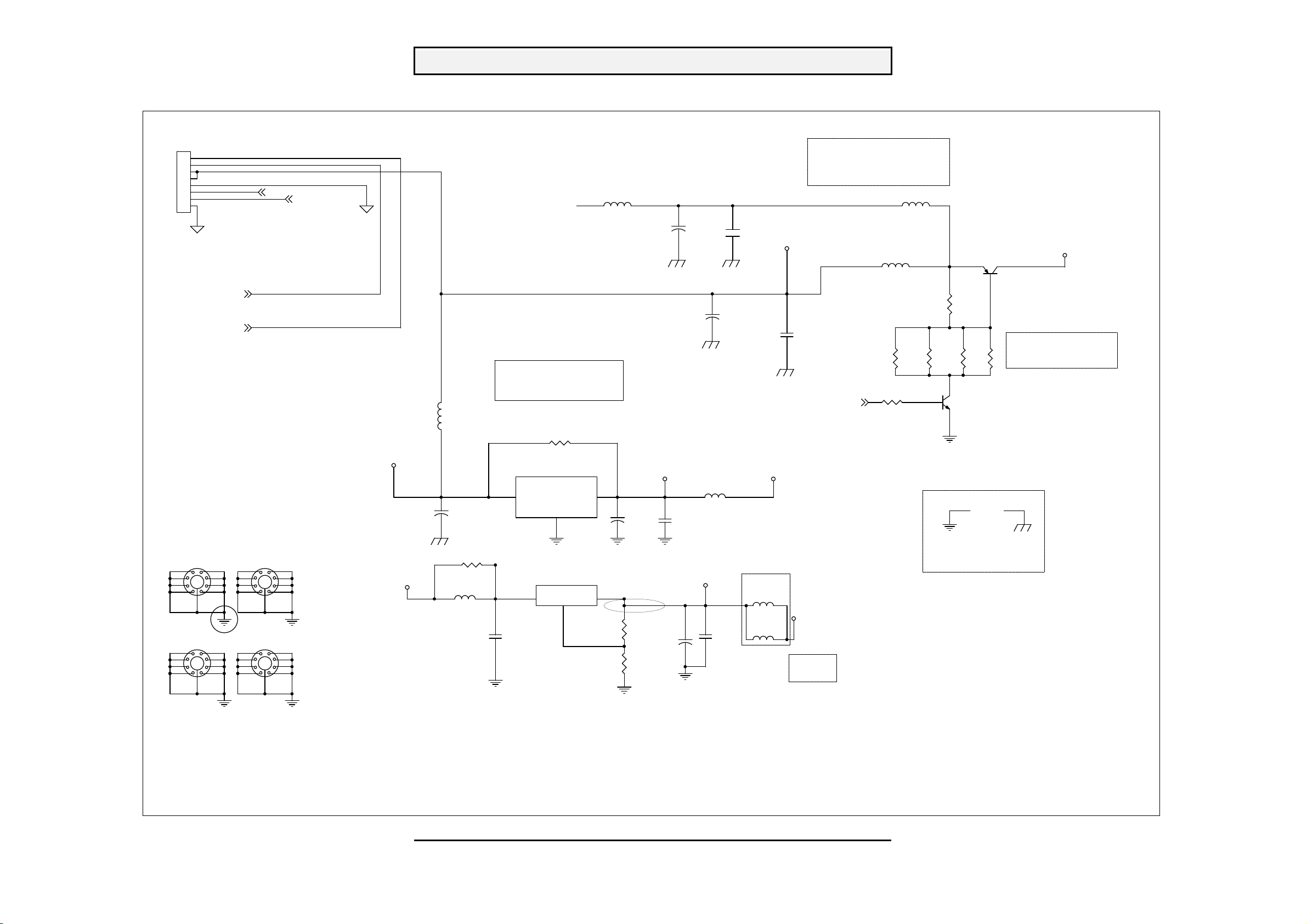
Page 13
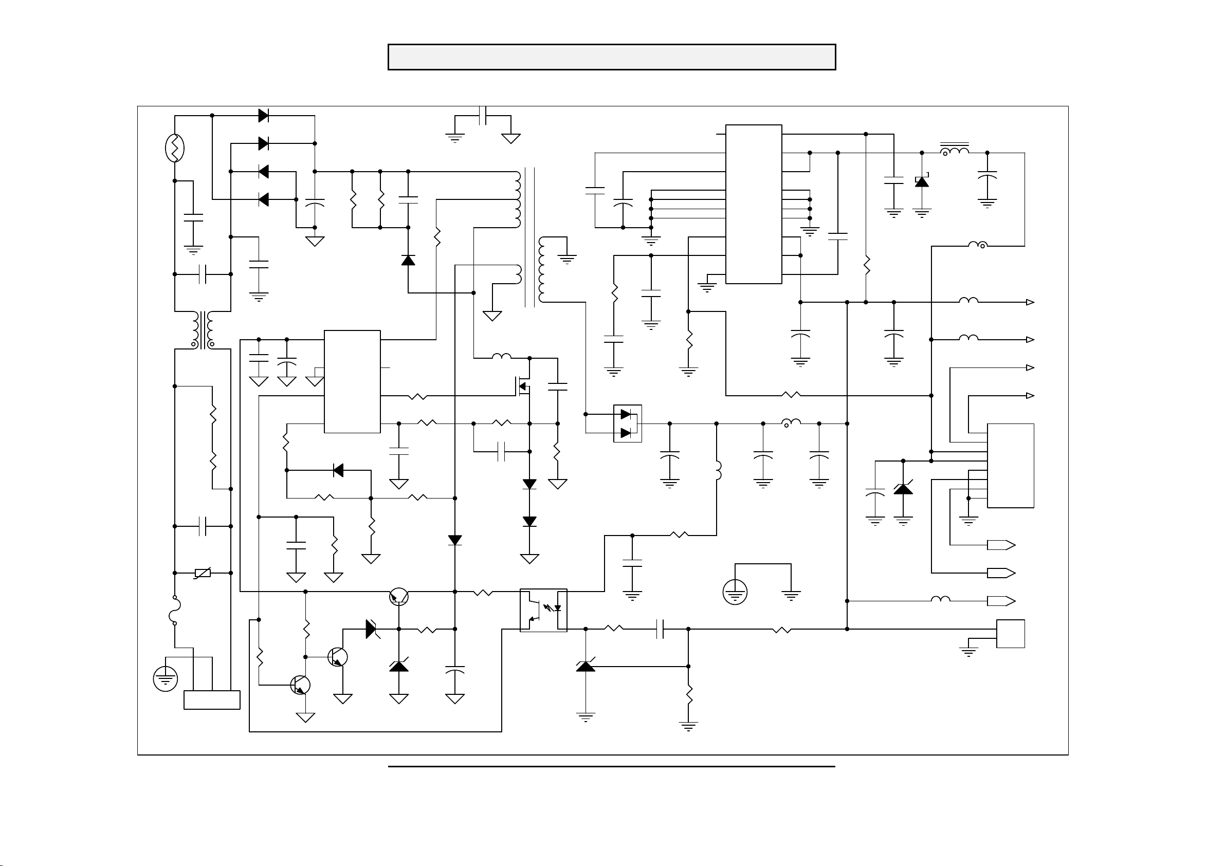
6.6. POWER PCB
787LE Service Manual
D805 2A07
R840
D807 2A07
10 3A
D810 2A07
D813 2A07
C802
4700PF
Y1
C824
0.22UF
C811
0.1uF
L805
ET-20
R833
470K
R801
470K
C801
0.22UF
R803
NC
F801
2.5A/250V
L
R
G
P801
AC IN 100-240V
C803
4700PF
Y1
C808
100uF/25V
C804
22nF
R820
47K
R818
68K
Q804
2SC945
100K/1W
+
C812
120uF/400V
TEA1533AP
1
Vcc
+
2
GND
3
Ctrl
4 5
DEMSense
R821
39K 1%
R823
1K
7A3(6.8V)
R804
I801
Drain
HVS
Driver
D801
1N4148
D808
Q803
2SC945
10nF/630V
R802
100K/1W
D802
1H7G
8
7
6
R816
10K 1%
2SC2120
D809
15-2
C806
R807 10
R806 470
C805
1000PF
R814 33K1%R822 200K 1%
Q802
R819
4K7
R805
1
D806
1H5G
+
C810
22uF/25V
C823
4700PF
Y1
PQ-2620
1
2
3
5
6
L802
BEAD
Q801
A09N70I
R826 12K
C807 22nF
D803
1U5G
D811
1U5G
4
R817
4K7
3
T801
C809
220PF 1KV
I802
TLP721F
I803
TL431
C832
470nF
10-12
7-9
R810
0.15/2W
R809
9K1 1%
1
2
+
C831
1uF/50V
C822
22nF
D804
FCH30A15
R813
100
C818
220PF
R865
10K 1%
+
C821
1500UF/16V
R815 120
C819
2200PF
C820
0.1UF
R812
2.43K 1%
I804 L4973
20
Sync
19
SS
18
V5.1
17
Gnd
16
Gnd
15
Gnd
14
Gnd
13
Vfb
12
COMP
L809
BEAD
Out
Out
Vcc
Vcc
1
2
3
4
5
6
7
8
9
1011
OSC
Gnd
Gnd
Gnd
Gnd
BootINH
C829
680UF/16V
R808 150 1%
L804
+
5UH
C813
1500UF/16V
R811
9.1K 1%
C828
220nF
+
+
C816
1500UF/16V
C814
2.7nF
R824
20K 1%
C830
680uF/16V
C833
680uF/16V
+
D814
6V2
L812
115uH
+
D812
SR560
C826
680uF/16V
L806
28UH
TO Inverter
L810
+
BEAD
TO Inveter
L803
BEAD
TO Inverter
TO Inverter
8
ON/OFF
7
Brigntness
6
5V
5
5V
4
GND
3
Standby
2
Volume
1
GND
P802
TO Audio
TO Audio
TO Audio
L811
NC
1
12V
2
GND
P805
-12-
9/24/2003
Page 14

6.7. INVERTER
787LE Service Manual
12V
C918
220uF/25V
5V
C815
220uF/16V
Brightness
R902 39K 1%
ON/OFF
C903 1uF
C905 0.1UF
C902 0.1UF
C906 0.47uF
C932
0.1uF
+
+
+
R905
10K
10uF/50V
+
R906 NC
C908
0.01UF
C901 220uF/25V
R933
100K
R904
R901
47K 1%
15
C917
C907 4.7uF/16V
10 11
C909
1500PF
Q905
2N7000
R934
220K
R903
51.1k 1%
C904
1uF/50V
1
CTIMR
2
OVP
3
ENA
4
SST
5
VDDA
6
GNDA
7
REF
8
RT1
9
FB
CMPNDR_D
I901 OZ960
Q906
2N7000
C933
0.1uF
+
NDR_B
PDR_A
CT
RT
PGND
LCT
DIM
LPWM
PDR_C
D920
9.1V
R932
10K
20
19
18
17
16
15
14
13
12
R909
10K
C913
47nF
R926
4.7
R925
4.7
C912 220PF
R908 62K 1%
C911
0.01UF
R907 27K
R931 4.7
R930 4.7
D919
5.6V
D918 SS14
4 5
3
2
1
D921 SS14
R915 10K
D908 5.6V
C910
47nF
Q903
2SC945
C914
2.2uF
G1D1
S1
D1
G2
D2
S2
D2
C915
2.2uF
6
7
8
I902
AOP600
D922 SS14
4 5
G1D1
3
S1
2
G2
1
S2
D923 SS14
R927
100K
R923
39K
D1
D2
D2
6
7
8
2 8
5 9
L901
EEL-19
24:2400
2 8
5 9
L903
EEL-19
24:2400
I903
AOP600
Q901
2N7000
Q902
2N7000
D905
1N4148
R914
1M
D910
1N4148
D911
1N4148
R919
51K
R921
1M
R922
1M
D904
1N4148
C928
5PF 3KV
C929
8200PF
C930
5PF 3KV
C931
8200PF
D916
1N4148
C926
0.1uF
D917
1N4148
C927
0.1uF
C919
1
47PF 3KV
3
C920 47PF 3KV
R912
499 1%
D914
1N4148
C924 47PF 3KV
C925
47PF 3KV
1N4148
R920
10K
L904
EE-8.3
1
3
R917
499 1%
D915
270 1%
2
4
D906
1N4148
R913
270 1%
L905
EE-8.3
1N4148
R918
2
4
D912
4
3
2
1
D907
1N4148
4
3
2
1
D913
1N4148
P901
H
H
NC
L
P906
H
H
NC
L
R916
390K
C916
0.1uF
Q904
2SA733
-13-
9/24/2003
Page 15

787LE Service Manual
7. WORKING THEOREM
A. DC-DC CONVERTER
This brick convert is the 12V input voltage to 5V output for panel use and system controller use .
It consists of a PWM IC (L4973 I804), flywheel diode (D812 SR560), buck choke (L812) and
capacitor C826.
I804 (L4973) is a PWM generator working at 200KHz.
5V Out put at 2,3 pin
VCC 12V In put at 8 pin
B. Scaling controller
The ADC is to convert RGB analog signal to digital signal that scaling chip can acknowledge.
The HSYNC input receives a logic signal and provides the frequency reference for pixel clock
generation.
The scaling IC is to converts the input signal ranging from VGA to SXGA into SXGA resolution
that panel can acknowledge.
The scaling IC is to converts the input signal ranging from VGA to SXGA into SXGA resolution
that panel can acknowledge.
When power is first applied, the ADE3XXX is asynchronously reset from a pin. The uC typically
programs the ADE3XXX with a number of default values and sets up the ADE3XXX to identify
activity on any of the input pins. All preconfigured values and RAMs, such as DVI settings,
line-lock PLL settings, video input modes (YUV), OSD characters, LCD timing values (output
sequencer), scale kernels, gamma curves, sRGB color warp, APC dithering, output pin
configuration (OMUX), etc. can be preloaded into the ADE3XXX.
The typical end state is that the ADE3XXX is initialized into a low power mode, ready to turn
active once the power button is pressed. activity detect When the monitor has been powered on,
the inputs can be monitored for active video sources. Based on the activity monitors, the uC
chooses an input or power down state.
SMEAS 40 sync / timing measurement Once an input source is selected, all available information
on frequencies and line/pixel counts is measured for the selected source and made available to the
uC.
SMEAS 40 mode set Once the uC has determined the matching video mode or calculated a video
mode using a GTF algorithm, the datapath is programmed to drive the flat panel. Clock
frequencies for the internal memory and datapath are also set at this time. autotune When the uC
calls for an autotune, the uC sets up an iterative loop to search for the best phase, gain, offset, etc.
At each step of the loop, the uC kicks off a test in which the ADE3XXX which performs extensive
statistical analysis of the incoming data stream. The results of the analysis are made available to
the uC which is responsible for the optimization algorithmSRT digital contrast / brightness In
response to user OSD control, the uC can program single 8b registers that set brightness and
contrast for each color channel independently.
SRGB 80 white point control In response to user OSD control, the uC can program three 8b
registers that set the white point for the output.
SRGB 80 gamma adjustment The uC can program the gamma RAMs to implement 10b accurate
color transformations.
GAMMA 92 sRGB control The SRGB block allows simple, intuitive color control with just a few
registers.
SRGB 80 pattern generation For production testing, the ADE3XXX can be programmed by the uC
to output a wide set of test patterns.
PGEN 74 flicker reduction For smart panel applications, the uC can set up the flicker detection
block to report any correlation with the polarity inversion signal. The uC can then change the
polarity inversion to a non-correlating pattern to eliminate flicker.
HDCP The ADE3XXX contains the BlockCipher and Decryption functions - interactions over
DDC are managed by the uC for maximum flexibility. The uC models the slow (frame rate, e.g.
60Hz) authentication handshaking and state machine whereas the ADE3XXX handles the fast (line
rate, e.g. 50kHz) decryption state machine.
HDCP 34 backlight control The ADE3XXX provides two PWM outputs for direct control of the
-14-
8/25/2003
Page 16

787LE Service Manual
power components in a typical backlight. The uC sets up the registers and enables the function.
PWM 97
Table 1: Pin Description
Pin # Name Type Description
1 YUV6 Input TV Video input port: Data 6
2 YUV5 Input TV Video input port: Data 5
3 YUV4 Input TV Video input port: Data 4
4 YUV3 Input TV Video input port: Data 3
5 YUV2 Input TV Video input port: Data 2
6 YUV1 Input TV Video input port: Data 1
7 YUV0 Input TV Video input port: Data 0
8 YUVCLK Input TV Video input port: Clock
9 DVDD18 Power Digital 1.8V VDD
10 DGND Power Digital Ground
11 DVDD18 Power Digital 1.8V VDD
12 DGND Power Digital Ground
13 AGND Power Analog Ground
14 AVDD18 Power Analog 1.8V VDD
15 AVDD33 Power Analog 3.3V VDD
16 RX2M Input DVI Receiver Channel 2 MINUS input (RED)
17 RX2P Input DVI Receiver Channel 2 PLUS input (RED)
18 AGND Power Analog Ground
19 AVDD33 Power Analog 3.3V VDD
20 RX1M Input DVI Receiver Channel 1 MINUS input (GREEN)
21 RX1P Input DVI Receiver Channel 1 PLUS input (GREEN)
22 AVDD33 Power Analog 3.3V VDD
23 RX0M Input DVI Receiver Channel 0 MINUS input (BLUE)
24 RX0P Input DVI Receiver Channel 0 PLUS input (BLUE)
25 AVDD33 Power Analog 3.3V VDD
26 AGND Power Analog Ground
27 RXCP Input DVI Receiver Clock Channel PLUS input
28 RXCM Input DVI Receiver Clock Channel MINUS input
29 AVDD33 Power Analog 3.3V VDD
30 REXT Passive 1% 475 Ohm resistor to Analog 3.3V VDD
31 AVDD33 Power Analog 3.3V VDD
32 AVDD33 Power Analog 3.3V VDD
33 AGND Power Analog Ground
34 AGND Power Analog Ground
35 AGND Power Analog Ground
36 RBIAS Passive 1% 2.0 kOhm resistor to Analog Ground
37 AGND Power Analog Ground
38 AVDD18 Power Analog 1.8V VDD
39 AGND Power Analog Ground
40 AVDD33 Power Analog 3.3V VDD
41 AGND Power Analog Ground
42 AVDD18 Power Analog 1.8V VDD
43 AGND Power Analog Ground
44 AVDD18 Power Analog 1.8V VDD
45 AGND Power Analog Ground
46 AVDD18 Power Analog 1.8V VDD
47 XGND Power Crystal Oscillator Ground
48 XTAL_IN Input Crystal Oscillator input
49 XTAL_OUT Output Crystal Oscillator output
50 XVDD18 Power Crystal Oscillator 1.8V VDD
51 LVDD18 Power Line Lock PLL 1.8V VDD
52 LGND Power Line Lock PLL Ground
-15-
8/25/2003
Page 17

787LE Service Manual
53 CSYNC Input Composite Sync Input - for Sync On Green
54 VSYNC Input Vertical Sync Input
55 HSYNC Input Horizontal (or Composite) Sync Input
56 AGND Power Analog Ground
57 AGND Power Analog Ground
58 AVDD33 Power Analog 3.3V VDD
59 AVDD33 Power Analog 3.3V VDD
60 AGND Power Analog Ground
61 AVDD18 Power Analog 1.8V VDD
62 AGND Power Analog Ground
63 REFB Passive 1% 15.0 kOhm resistor to Analog Ground
64 REFMB Passive connect to Analog Ground
65 REFPB Passive 470nF capacitor to Analog Ground
66 AGND Power Analog Ground
67 AGND Power Analog Ground
68 INB Input Analog Video Port: Blue Channel input
69 AVDD33 Power Analog 3.3V VDD
70 AVDD33 Power Analog 3.3V VDD
71 REFCB Passive 100nF capacitor to Analog Ground
72 AGND Power Analog Ground
73 AVDD18 Power Analog 1.8V VDD
74 AVDD18 Power Analog 1.8V VDD
75 REFG Passive 1% 15.0 kOhm resistor to Analog Ground
76 REFMG Passive connect to Analog Ground
77 REFPG Passive 470nF capacitor to Analog Ground
78 AGND Power Analog Ground
79 AGND Power Analog Ground
80 ING Input Analog Video Port: Green Channel input
81 AVDD33 Power Analog 3.3V VDD
82 AVDD33 Power Analog 3.3V VDD
83 REFCG Passive 100nF capacitor to Analog Ground
84 AGND Power Analog Ground
85 AVDD18 Power Analog 1.8V VDD
86 AVDD18 Power Analog 1.8V VDD
87 REFR Passive 1% 15.0 kOhm resistor to Analog Ground
88 REFMR Passive connect to Analog Ground
89 REFPR Passive 470nF capacitor to Analog Ground
90 AGND Power Analog Ground
91 AGND Power Analog Ground
92 INR Input Analog Video Port: Red Channel input
93 AVDD33 Power Analog 3.3V VDD
94 AVDD33 Power Analog 3.3V VDD
95 REFCR Passive 100nF capacitor to Analog Ground
96 AGND Power Analog Ground
97 AVDD18 Power Analog 1.8V VDD
98 AVDD18 Power Analog 1.8V VDD
99 TST_SCAN Input connect to Digital Ground
100 DGND Power Digital Ground
101 DVDD33 Power Digital 3.3V VDD
102 OBA7 Output Output Port A: Blue Data 7
103 OBA6 Output Output Port A: Blue Data 6
104 OBA5 Output Output Port A: Blue Data 5
105 DGND Power Digital Ground
106 OBA4 Output Output Port A: Blue Data 4
107 OBA3 Output Output Port A: Blue Data 3
108 OBA2 Output Output Port A: Blue Data 2
109 OBA1 Output Output Port A: Blue Data 1
-16-
8/25/2003
Page 18

787LE Service Manual
110 OBA0 Output Output Port A: Blue Data 0
111 DVDD33 Power Digital 3.3V VDD
112 DGND Power Digital Ground
113 OGA7 Output Output Port A: Green Data 7
114 OGA6 Output Output Port A: Green Data 6
115 OGA5 Output Output Port A: Green Data 5
116 OGA4 Output Output Port A: Green Data 4
117 OGA3 Output Output Port A: Green Data 3
118 OGA2 Output Output Port A: Green Data 2
119 OGA1 Output Output Port A: Green Data 1
120 OGA0 Output Output Port A: Green Data 0
121 DVDD18 Power Digital 1.8V VDD
122 DGND Power Digital Ground
123 DVDD18 Power Digital 1.8V VDD
124 DGND Power Digital Ground
125 DVDD33 Power Digital 3.3V VDD
126 ORA7 Output Output Port A: Red Data 7
127 ORA6 Output Output Port A: Red Data 6
128 ORA5 Output Output Port A: Red Data 5
129 ORA4 Output Output Port A: Red Data 4
130 ORA3 Output Output Port A: Red Data 3
131 ORA2 Output Output Port A: Red Data 2
132 ORA1 Output Output Port A: Red Data 1
133 ORA0 Output Output Port A: Red Data 0
134 DVDD33 Power Digital 3.3V VDD
135 DGND Power Digital Ground
136 ODE Output Output Data Enable
137 OHS Output Output Horizontal Sync
138 OCLK Output Output Clock
139 OVS Output Output Vertical Sync
140 DVDD18 Power Digital 1.8V VDD
141 DGND Power Digital Ground
142 DVDD18 Power Digital 1.8V VDD
143 DGND Power Digital Ground
144 OBB7 Output Output Port B: Blue Data 7
145 OBB6 Output Output Port B: Blue Data 6
146 OBB5 Output Output Port B: Blue Data 5
147 OBB4 Output Output Port B: Blue Data 4
148 DVDD33 Power Digital 3.3V VDD
149 DGND Power Digital Ground
150 OBB3 Output Output Port B: Blue Data 3
151 OBB2 Output Output Port B: Blue Data 2
152 OBB1 Output Output Port B: Blue Data 1
153 OBB0 Output Output Port B: Blue Data 0
154 OGB7 Output Output Port B: Green Data 7
155 OGB6 Output Output Port B: Green Data 6
156 OGB5 Output Output Port B: Green Data 5
157 OGB4 Output Output Port B: Green Data 4
158 DVDD33 Power Digital 3.3V VDD
159 DGND Power Digital Ground
160 OGB3 Output Output Port B: Green Data 3
161 OGB2 Output Output Port B: Green Data 2
162 OGB1 Output Output Port B: Green Data 1
163 OGB0 Output Output Port B: Green Data 0
164 DVDD18 Power Digital 1.8V VDD
165 DGND Power Digital Ground
166 DVDD18 Power Digital 1.8V VDD
-17-
8/25/2003
Page 19

787LE Service Manual
167 DGND Power Digital Ground
168 ORB7 Output Output Port B: Red Data 7
169 ORB6 Output Output Port B: Red Data 6
170 ORB5 Output Output Port B: Red Data 5
171 ORB4 Output Output Port B: Red Data 4
172 DVDD33 Power Digital 3.3V VDD
173 DGND Power Digital Ground
174 ORB3 Output Output Port B: Red Data 3
175 ORB2 Output Output Port B: Red Data 2
176 ORB1 Output Output Port B: Red Data 1
177 ORB0 Output Output Port B: Red Data 0
178 DVDD18 Power Digital 1.8V VDD
179 DGND Power Digital Ground
180 DVDD18 Power Digital 1.8V VDD
181 DGND Power Digital Ground
182 CLKOUT Output not to be connected - reserved
183 CLKIN Input to be connected to Digital Ground - reserved
185 DVDD33 Power Digital 3.3V VDD
186 DGND Power Digital Ground
191 DVDD18 Power Digital 1.8V VDD
192 DGND Power Digital Ground
193 DVDD18 Power Digital 1.8V VDD
194 DGND Power Digital Ground
199 DVDD18 Power Digital 1.8V VDD
200 DGND Power Digital Ground
201 DVDD18 Power Digital 1.8V VDD
202 DGND Power Digital Ground
203 SCL Input I2C Clock
204 SDA Open Drai
205 XCLK Output Crystal clock buffered output
206 XCLK_EN Input Crystal clock output enable
0 : xclk output disabled
1 : xclk output active
207 RESETN Input Reset input, Active Low
MTV312M64
The MTV312M micro-controller is an 8051 CPU core embedded device especially tailored for
CRT/LCD
Monitor applications. It includes an 8051 CPU core, 1024-byte SRAM, 14 built-in PWM DACs,
VESA DDC interface, 4-channel A/D converter, and a 64K-byte internal program Flash-ROM.
A “CMOS output pin” means it can sink and drive at least 4mA current. It is not recommended to
use such
pin as input function.
A “open drain pin” means it can sink at least 4mA current but only drive 10~20uA to VDD. It can
be used as input or output function and needs an external pull up resistor.
A “8051 standard pin” is a pseudo open drain pin. It can sink at least 4mA current when output is
at low level, and drives at least 4mA current for 160nS when output transits from low to high, then
keeps driving at 100uA to maintain the pin at high level. It can be used as input or output function.
It needs an external pull up resistor when driving heavy load device.
POWER CONFIGURATION
The MTV312M can work on 5V or 3.3V power supply system.
In 5V power system, the VDD pin is connected to 5V power and the VDD3 needs an external
capacitor, all
output pins can swing from 0~5V, input pins can accept 0~5V input range.
And ADC conversion range is 5V. However, X1 and X2 pins must be kept below 3.3V.
-18-
8/25/2003
Page 20

787LE Service Manual
In 3.3V power system, the VDD and VDD3 are connected to 3.3V power, all output pins swing
from 0~3.3V, HSYNC, VSYNC and open drain pin can accept 0~5V input range, other pins must
be kept below 3.3V. And the ADC conversion range is 3.3V.
INVERTER
In order to drive the CCFLs embedded in the panel module, there is a half bridge inverter to
convert by the controller.
The input 12V up to hundreds of AC voltage output.
The inverter is formed by symmetric in order to drive the separate lamp modules.
The input stage consists of a PWM controller, half bridge inverter, and switching MOSFET to
convert DC input into AC output.
The output stage consists of a tuning capacitor, coupling capacitor, transformer, push-pull
MOSFET pair to boost AC output up to hundreds of voltage.
And one resister is serial to lamp for output voltage feedback.
There are two signal to control the inverter which come from system.
Logic “high” level which send to I901 is turn on the inverter.
BRI signal control brightness by DC level which was integral from PWM signal.
-19-
8/25/2003
Page 21

8. Wiring Diagram
787LE Service Manual
LCD PANEL
P981
P901
POWER PCB
P906
TO:METAL FITTG
GND
P802
P601
P953
P701
P701
KEYPAD PCB
P101 P105
MAIN PCB
P103
P104
P961
I/O CABLE
-20-
8/25/2003
Page 22

9. PCB Layout
9.1. MAIN PCB TOP VIEW
787LE Service Manual
-21-
8/25/2003
Page 23

9.2. MAIN PCB BOTTOM VIEW
787LE Service Manual
-22-
8/25/2003
Page 24

9.3. CON PCB TOP VIEW
787LE Service Manual
-23-
8/25/2003
Page 25

9.4. CON PCB BOTTOM VIEW
787LE Service Manual
-24-
8/25/2003
Page 26

9.5. POWER PCB TOP VIEW
787LE Service Manual
-25-
8/25/2003
Page 27

9.6. POWER PCB BOTTOM VIEW
787LE Service Manual
-26-
8/25/2003
Page 28

787LE Service Manual
10. TROUBLE SHOOTING FLOW CHART
10.1. NO POWER
POWER
STAR
Check
12V O/P
D804
Check F801
D805,D807
D810,D813
Check
I801
,Q801
STAR
12V
Check
5V O/P
C826
Check
I804
D812
P802 5,6 PIN
5V
12V
Check
Check
P901,P906
Check I101
L901,L903
L904,L905
D918,D922
Check
I901
MAIN PCB
PANEL
CHECK
MAIN PCB
5V OK?
Y
3.3V OK?
Y
1.8V OK?
N
N
N
CHECK
POWER PCB
OK?
CHECK
I103,
SUROUND CAP
BEAD OK?
CHECK
I104,
SUROUND CAP
BEAD OK?
-27-
CHECK
I106,I107
SUROUND CAP
OK?
CHECK
I101,
SUROUND CAP
BEAD OK?
8/25/2003
Page 29

10.2. MCU NO FUNCTION
787LE Service Manual
CHECK
C239
MCU 5V
OK?
Y
CHECK
I108 PIN7,PIN9
5V?
Y
CHECK
12MHz PIN11,PIN12
OK?
Y
CHECK
PIN13,PIN14
CLOCK OK?
N
N
N
N
CHECK
Q108,Q107
OK?
CHECK
R190,C219
OK?
CHECK
X102,C222,C223
OK?
CHECK
I108 TO I101
OK?
Y
CHECK
I108,EVERY TWO
PIN SHORT?
N
CHECK
KEYPAD P103
OK?
-28-
8/25/2003
Page 30

10.3. NO DISPLAY
787LE Service Manual
Power Key Work
OK?
Y
Check
H V sync
Y
Check R.G.B
DATA
Y
Check
X101,X102
Y
Check I101
OCLK,ODE,
OVS,OHS
N
N
N
N
N
Check
Keypad
Check
I105
CHECK
I/O cable
Check
C162,C163,
C222,C223
Check
ADE SCL,SDA
N
N
N
R197,R198,R199
N
N
Check
5V MCU
Check
P104
Check
Check
I104,I103
Check
I108,SCL,SDA
N
N
N
N
N
Check
I108
Check
I/O cable
Check
I101
Check
Avdd 1.8V,3.3V
Check
I109,SCL,SDA
Y
Check
I106,I107
N
Check
Q102
N
Check
INVERTER
N
Check
PANEL
-29-
8/25/2003
Page 31

10.4. LOSE COLOR
787LE Service Manual
Some bits
Lost
Y
Check
RP01~RP12
I106 poor
soldering
P105
soldering
N
N
I101 or R-pack
soldering
Y
I107 poor
soldering
Lose color
R or G or B
Y
Check
P104
Pin 8,10,12
Y
Check
L120,121,122
R122,125,127
Y
I101
fail or poor
soldering
N
N
Check
Sign Cable
Check
C182,183,186
R197,198,199
-30-
8/25/2003
Page 32

787LE Service Manual
1
2
2
11. ADJUSTMENT
11.1. ADJUSTMENT CONDITIONS AND PRECAUTIONS
1. Approximately 30 minutes should be allowed for warm up before proceeding.
2. Adjustments should be undertaken only on those necessary elements since most of them
have been carefully preset at the factory.
3. ESD protection is needed before adjustment.
11.2. MAIN ADJUSTMENTS
1. WHITE BALANCE FUNCTION KEY
2. GEOMETRY FUNCTION KEY
NO. FUNCTION DESIGNATION
11.3. ALIGNMENT PROCEDURES
Adjustment Conditions and Precautions:
(A). Power supply voltage:
AC 110/120V±10% 60 Hz±5%, AC 220/240V±10% 50 Hz±5%.
(B). Warm up time:
The display must be power ON for at least 30 minutes at full white pattern before
starting alignments.
This is especially critical in color temperature and white balance adjustments.
(C). Signals: reference the front detail specifications and timing table.
Video : reference the front detail specifications.
1. Adjustment of White Balance:
A. TIMING: 1280x1024 64KHz/60Hz.
B. PATTERN: 5 Blocks.
C. LCD MONITOR set to 1280x1024 80K/75Hz BURN IN and warm up over 30 minutes.
D. CA110 color analizer at the center of screen and along a perpendicular to the screen at
20cm from the display.
E. Power turn off, Press
LED ison, release
(Fig.1)
“▲” and “ ”
“▼” and “ ”
-31-
and turn on power at the same time after power
key, Then press “ ” key go to factory mode.
(Fig.1)
8/25/2003
Page 33

787LE Service Manual
2
2
2
2 1 2 2 1
F. Adjust Color Temperature:
(1) EEPROM INIT (5 BLOCKS):
Press “▼” key move cursor to EEPROM INIT, Press key then monitor will
INIT ADC value.
(2) Press “▲” key move cursor to “White Balance”, Press key do white balance
adjustment.
(3) Press “▼” key move cursor to “Color Temerature Adjust”, Press key, Then
OSD will display Fig.2
(4) 9300K verify: move cursor to 9300K Press key.
Press “▼” ,“▲” key adjust R.G.B value
x=0.283 ±0.03
y=0.298 ±0.03
Press key return to Fig.2
(5) 6500K verify: Repeat (4) press “▼” ,“▲” move cursor to 6500K press key
x=0.310 ±0.03
y=0.330 ±0.03
Y≧200 cd/m2
(6) Press key go back to Fig.2, Then press key return to Fig.1, Power key
OFF/ON quit factory mode.
G. Color Temperature & Luminance Verify:
BRIGHTNESS MAX, CONTRAST MAX
9300K: x=0.283 ±0.03 y=0.298 ±0.03
6500K: x=0.310 ±0.03 y=0.330 ±0.03 Y≧200 cd/m2
2. Geometry:
(a). Set cross-hatch pattern and preset timing as timing table listed.
(b). Change to each mode in turn and wait for the monitor finish auto-alignment and save
process before change to next mode.
(c). Until all of modes are agjusted, exit OSD menu and press PWR OFF to exit factory
mode.
(Fig.2)
-32-
8/25/2003
Page 34

787LE Service Manual
12. ELECTRICAL PARTS LIST
When you place a parts order, be sure to indicate the following data on the order:
l Location No.
l Parts No.
l Description
LOC NO. SOURCE PART NO. DESCRIPTION SPECIFICATION REMARK
MAIN P.C.BOARD
C101 2333347613 CAP,ELE 105'C EC 47u/ 16V 5*11 P=2.5
C102 2346410496 CAP,CHIP 85'C CS 0603/Y5V/50V 0.1u Z
C104 2346410496 CAP,CHIP 85'C CS 0603/Y5V/50V 0.1u Z
C105 2346410496 CAP,CHIP 85'C CS 0603/Y5V/50V 0.1u Z
C107 2346410496 CAP,CHIP 85'C CS 0603/Y5V/50V 0.1u Z
C109 2346410496 CAP,CHIP 85'C CS 0603/Y5V/50V 0.1u Z
C110 2346410496 CAP,CHIP 85'C CS 0603/Y5V/50V 0.1u Z
C111 2346410496 CAP,CHIP 85'C CS 0603/Y5V/50V 0.1u Z
C112 2346410496 CAP,CHIP 85'C CS 0603/Y5V/50V 0.1u Z
C113 2346110296 CAP,CHIP 125'C CS 0603/X7R/50V 1000p K
C114 2346110396 CAP,CHIP 125'C CS 0603/X7R/50V 0.01u K
C115 2341110196 CAP,CHIP 125'C CS 0603/COG/50V 100p J
C116 2346410496 CAP,CHIP 85'C CS 0603/Y5V/50V 0.1u Z
C117 2346110296 CAP,CHIP 125'C CS 0603/X7R/50V 1000p K
C118 2346110396 CAP,CHIP 125'C CS 0603/X7R/50V 0.01u K
C119 2346410496 CAP,CHIP 85'C CS 0603/Y5V/50V 0.1u Z
C120 2346110396 CAP,CHIP 125'C CS 0603/X7R/50V 0.01u K
C121 2333347613 CAP,ELE 105'C EC 47u/ 16V 5*11 P=2.5
C122 2333347613 CAP,ELE 105'C EC 47u/ 16V 5*11 P=2.5
C123 2333347613 CAP,ELE 105'C EC 47u/ 16V 5*11 P=2.5
C124 2346410496 CAP,CHIP 85'C CS 0603/Y5V/50V 0.1u Z
C125 2346410496 CAP,CHIP 85'C CS 0603/Y5V/50V 0.1u Z
C126 2346410496 CAP,CHIP 85'C CS 0603/Y5V/50V 0.1u Z
C127 2346410496 CAP,CHIP 85'C CS 0603/Y5V/50V 0.1u Z
C128 2346410496 CAP,CHIP 85'C CS 0603/Y5V/50V 0.1u Z
C129 2346410496 CAP,CHIP 85'C CS 0603/Y5V/50V 0.1u Z
C130 2346410496 CAP,CHIP 85'C CS 0603/Y5V/50V 0.1u Z
C131 2346410496 CAP,CHIP 85'C CS 0603/Y5V/50V 0.1u Z
C132 2346410496 CAP,CHIP 85'C CS 0603/Y5V/50V 0.1u Z
C133 2346410496 CAP,CHIP 85'C CS 0603/Y5V/50V 0.1u Z
C134 2346410496 CAP,CHIP 85'C CS 0603/Y5V/50V 0.1u Z
C135 2346410496 CAP,CHIP 85'C CS 0603/Y5V/50V 0.1u Z
C136 2346410496 CAP,CHIP 85'C CS 0603/Y5V/50V 0.1u Z
C137 2346410496 CAP,CHIP 85'C CS 0603/Y5V/50V 0.1u Z
C138 2346410496 CAP,CHIP 85'C CS 0603/Y5V/50V 0.1u Z
C139 2333347613 CAP,ELE 105'C EC 47u/ 16V 5*11 P=2.5
C140 2346410496 CAP,CHIP 85'C CS 0603/Y5V/50V 0.1u Z
C141 2346410496 CAP,CHIP 85'C CS 0603/Y5V/50V 0.1u Z
C142 2346410496 CAP,CHIP 85'C CS 0603/Y5V/50V 0.1u Z
C143 2346410496 CAP,CHIP 85'C CS 0603/Y5V/50V 0.1u Z
C144 2346410496 CAP,CHIP 85'C CS 0603/Y5V/50V 0.1u Z
C145 2346410496 CAP,CHIP 85'C CS 0603/Y5V/50V 0.1u Z
C146 2346410496 CAP,CHIP 85'C CS 0603/Y5V/50V 0.1u Z
C147 2346410496 CAP,CHIP 85'C CS 0603/Y5V/50V 0.1u Z
C148 2333347613 CAP,ELE 105'C EC 47u/ 16V 5*11 P=2.5
C149 2346410496 CAP,CHIP 85'C CS 0603/Y5V/50V 0.1u Z
C150 2346410496 CAP,CHIP 85'C CS 0603/Y5V/50V 0.1u Z
C151 2346410496 CAP,CHIP 85'C CS 0603/Y5V/50V 0.1u Z
C152 2346410496 CAP,CHIP 85'C CS 0603/Y5V/50V 0.1u Z
C153 2346747496 CAP,CHIP 85'C CS 0603/Y5V/16V 0.47u Z
C154 2341110196 CAP,CHIP 125'C CS 0603/COG/50V 100p J
C155 2346410496 CAP,CHIP 85'C CS 0603/Y5V/50V 0.1u Z
C156 2346747496 CAP,CHIP 85'C CS 0603/Y5V/16V 0.47u Z
C157 2341110196 CAP,CHIP 125'C CS 0603/COG/50V 100p J
C158 2346410496 CAP,CHIP 85'C CS 0603/Y5V/50V 0.1u Z
-33-
9/24/2003
Page 35

787LE Service Manual
LOC NO. SOURCE PART NO. DESCRIPTION SPECIFICATION REMARK
C159 2346747496 CAP,CHIP 85'C CS 0603/Y5V/16V 0.47u Z
C160 2341110196 CAP,CHIP 125'C CS 0603/COG/50V 100p J
C161 2346410496 CAP,CHIP 85'C CS 0603/Y5V/50V 0.1u Z
C162 2341122096 CAP,CHIP 125'C CS 0603/COG/50V 22p J
C163 2341122096 CAP,CHIP 125'C CS 0603/COG/50V 22p J
C164 2346410496 CAP,CHIP 85'C CS 0603/Y5V/50V 0.1u Z
C166 2333333791 CAP,ELE 105'C EC 330u/ 16V 8*11 P=5.0
C169 2346410496 CAP,CHIP 85'C CS 0603/Y5V/50V 0.1u Z
C170 2333447791 CAP,ELE 105'C EC 470u/ 25V 10*13.0 P=5.0
C171 2333347791 CAP,ELE 105'C EC 470u/ 16V 10*12.5 P=5.0
C176 2333333791 CAP,ELE 105'C EC 330u/ 16V 8*11 P=5.0
C177 2346410496 CAP,CHIP 85'C CS 0603/Y5V/50V 0.1u Z
C178 2346410496 CAP,CHIP 85'C CS 0603/Y5V/50V 0.1u Z
C179 2333347613 CAP,ELE 105'C EC 47u/ 16V 5*11 P=2.5
C180 2346410496 CAP,CHIP 85'C CS 0603/Y5V/50V 0.1u Z
C182 2346410496 CAP,CHIP 85'C CS 0603/Y5V/50V 0.1u Z
C183 2346410496 CAP,CHIP 85'C CS 0603/Y5V/50V 0.1u Z
C185 2341122096 CAP,CHIP 125'C CS 0603/COG/50V 22p J
C186 2346410496 CAP,CHIP 85'C CS 0603/Y5V/50V 0.1u Z
C191 2341122096 CAP,CHIP 125'C CS 0603/COG/50V 22p J
C192 2341147096 CAP,CHIP 125'C CS 0603/COG/50V 47p J
C194 2346410496 CAP,CHIP 85'C CS 0603/Y5V/50V 0.1u Z
C195 2346410496 CAP,CHIP 85'C CS 0603/Y5V/50V 0.1u Z
C196 2346410496 CAP,CHIP 85'C CS 0603/Y5V/50V 0.1u Z
C197 2346410496 CAP,CHIP 85'C CS 0603/Y5V/50V 0.1u Z
C198 2346410496 CAP,CHIP 85'C CS 0603/Y5V/50V 0.1u Z
C199 2346410496 CAP,CHIP 85'C CS 0603/Y5V/50V 0.1u Z
C200 2346110396 CAP,CHIP 125'C CS 0603/X7R/50V 0.01u K
C201 2346110296 CAP,CHIP 125'C CS 0603/X7R/50V 1000p K
C202 2346410496 CAP,CHIP 85'C CS 0603/Y5V/50V 0.1u Z
C203 2346410496 CAP,CHIP 85'C CS 0603/Y5V/50V 0.1u Z
C204 2346410496 CAP,CHIP 85'C CS 0603/Y5V/50V 0.1u Z
C205 2346410496 CAP,CHIP 85'C CS 0603/Y5V/50V 0.1u Z
C206 2346410496 CAP,CHIP 85'C CS 0603/Y5V/50V 0.1u Z
C207 2346410496 CAP,CHIP 85'C CS 0603/Y5V/50V 0.1u Z
C208 2346110396 CAP,CHIP 125'C CS 0603/X7R/50V 0.01u K
C209 2346110296 CAP,CHIP 125'C CS 0603/X7R/50V 1000p K
C215 2346410496 CAP,CHIP 85'C CS 0603/Y5V/50V 0.1u Z
C216 2346410496 CAP,CHIP 85'C CS 0603/Y5V/50V 0.1u Z
C217 2346410496 CAP,CHIP 85'C CS 0603/Y5V/50V 0.1u Z
C218 2346410496 CAP,CHIP 85'C CS 0603/Y5V/50V 0.1u Z
C219 2346410496 CAP,CHIP 85'C CS 0603/Y5V/50V 0.1u Z
C221 2341133096 CAP,CHIP 125'C CS 0603/COG/50V 33p J
C222 2341122096 CAP,CHIP 125'C CS 0603/COG/50V 22p J
C223 2341122096 CAP,CHIP 125'C CS 0603/COG/50V 22p J
C224 2346410496 CAP,CHIP 85'C CS 0603/Y5V/50V 0.1u Z
C232 2347710696 CAP,CHIP 85'C CS 0805/Y5V/10V 10u Z
C233 2347610596 CAP,CHIP 85'C CS 0805/Y5V/16V 1.0u Z
C234 2347610596 CAP,CHIP 85'C CS 0805/Y5V/16V 1.0u Z
C238 2346410496 CAP,CHIP 85'C CS 0603/Y5V/50V 0.1u Z
C239 2333347613 CAP,ELE 105'C EC 47u/ 16V 5*11 P=2.5
C240 2346410496 CAP,CHIP 85'C CS 0603/Y5V/50V 0.1u Z
C241 2333310613 CAP,ELE 105'C EC 10u/ 16V 5*11 P=2.5
C243 2333610613 CAP,ELE 105'C EC 10u/ 50V 5*11 P=2.5
D103 2364600196 DIODE,SWITCH SMD LL4148 3.5X1.5ö TEMIC GS08
D104 2364600196 DIODE,SWITCH SMD LL4148 3.5X1.5ö TEMIC GS08
D105 2364600196 DIODE,SWITCH SMD LL4148 3.5X1.5ö TEMIC GS08
D106 2364600196 DIODE,SWITCH SMD LL4148 3.5X1.5ö TEMIC GS08
D107 2364600196 DIODE,SWITCH SMD LL4148 3.5X1.5ö TEMIC GS08
D108 2364600196 DIODE,SWITCH SMD LL4148 3.5X1.5ö TEMIC GS08
D114 2364503996 DIODE,ZENER SMD BZV55-C5V6 PHILIPS
D115 2364503996 DIODE,ZENER SMD BZV55-C5V6 PHILIPS
D116 2364503996 DIODE,ZENER SMD BZV55-C5V6 PHILIPS
D117 2364503996 DIODE,ZENER SMD BZV55-C5V6 PHILIPS
D119 RA 2364201296 DIODE,RECT(SMD) BAT54C-7 SOT-23 DII
-34-
9/24/2003
Page 36

787LE Service Manual
LOC NO. SOURCE PART NO. DESCRIPTION SPECIFICATION REMARK
D119 RB 2364201896 DIODE,RECT(SMD) BAT54C CHENMKO SOT-23
D120 2364503996 DIODE,ZENER SMD BZV55-C5V6 PHILIPS
I101 2365928496 IC,DIGITAL SMD ADE3000SX PQFP208 ST
I103 RA 2365807496 IC,LINEAR(SMD) AIC1084-33CM AIC TO-263
I103 RB 2365810796 IC,LINEAR(SMD) AP1084K33A(3.3V) ATC TO-263
I104 RA 2365810896 IC,LINEAR(SMD) AP1117DA(ADJ) ATC TO-252
I104 RB 2365812096 IC,LINEAR(SMD) AIC1117CE-ADJ AIC TO-252
I105 RA 2365922496 IC,DIGITAL SMD 74LVC14A PHILIPS SO14
I105 RB 2365921996 IC,DIGITAL SMD SN74LVC14AD TI
I106 RA 2365920096 IC,DIGITAL SMD THC63LVDM83A THINE
I106 RB 2365917996 IC,DIGITAL SMD SN75LVDS83DGG TI
I106 RC 2365926196 IC,DIGITAL SMD NT7181CF TSSOP NOVATEK
I106 RD 2365928896 IC,DIGITAL SMD M385 TSSOP-56P MRT
I107 RA 2365920096 IC,DIGITAL SMD THC63LVDM83A THINE
I107 RB 2365917996 IC,DIGITAL SMD SN75LVDS83DGG TI
I107 RC 2365926196 IC,DIGITAL SMD NT7181CF TSSOP NOVATEK
I107 RD 2365928896 IC,DIGITAL SMD M385 TSSOP-56P MRT
I108 2365928596 IC,DIGITAL SMD MTV312MV64 PLCC44 MYSON
I109 RA 2365316200 IC,LINEAR 24LC16B DIP-8 MICROCHI
I109 RB 2365424300 IC,DIGITAL M24C16-WBN6T ST PDIP8
I109 RC 2365424000 IC,DIGITAL AM24LC16(PDIP-8L) ATC
L101 2379812156 BEAD,HI-IMPEDANCE Z= 120ohm( 1MHZ~) 0805 300mA
L102 2379812156 BEAD,HI-IMPEDANCE Z= 120ohm( 1MHZ~) 0805 300mA
L103 2379310166 BEAD,HI-IMPEDANCE Z= 100ohm( 50MHZ~) 0603 200mA
L106 2379560086 BEAD,HI-CURRENT Z= 60ohm 1206 I>3.0A
L107 2235547813 RES,MTL 2 RS 2WS 0.47ohm J P=15.0
L110 2379812156 BEAD,HI-IMPEDANCE Z= 120ohm( 1MHZ~) 0805 300mA
L111 2379812156 BEAD,HI-IMPEDANCE Z= 120ohm( 1MHZ~) 0805 300mA
L112 2379812156 BEAD,HI-IMPEDANCE Z= 120ohm( 1MHZ~) 0805 300mA
L113 2379812156 BEAD,HI-IMPEDANCE Z= 120ohm( 1MHZ~) 0805 300mA
L114 2379860166 BEAD,HI-IMPEDANCE Z= 600ohm( 50MHZ~) 0805 200mA
L115 2379860166 BEAD,HI-IMPEDANCE Z= 600ohm( 50MHZ~) 0805 200mA
L116 2379860166 BEAD,HI-IMPEDANCE Z= 600ohm( 50MHZ~) 0805 200mA
L117 2379860166 BEAD,HI-IMPEDANCE Z= 600ohm( 50MHZ~) 0805 200mA
L118 2379860166 BEAD,HI-IMPEDANCE Z= 600ohm( 50MHZ~) 0805 200mA
L119 2379560086 BEAD,HI-CURRENT Z= 60ohm 1206 I>3.0A
L120 2253200096 RES,CHIP 1/10W RC 0603 1/10W 0 ohm J T
L121 2253200096 RES,CHIP 1/10W RC 0603 1/10W 0 ohm J T
L122 2253200096 RES,CHIP 1/10W RC 0603 1/10W 0 ohm J T
L123 2379560086 BEAD,HI-CURRENT Z= 60ohm 1206 I>3.0A
L127 2379812156 BEAD,HI-IMPEDANCE Z= 120ohm( 1MHZ~) 0805 300mA
L131 2379560086 BEAD,HI-CURRENT Z= 60ohm 1206 I>3.0A
L132 2379560086 BEAD,HI-CURRENT Z= 60ohm 1206 I>3.0A
P101 2404301107 CONNECTOR JST PH 8P SIDE P=2.0 OR EQUAL
P103 2404371007 CONNECTOR JST PH 8P TOP P=2.0 OR EQUAL
P104 2404301112 CONNECTOR JST PH 13P SIDE P=2.0 OR EQUAL
P105 2404222230 PIN PLUG CH71302V1P3 P=2.0 30PIN CVILUX
Q101 RA 2360301696 XISTOR,NPN R SMD PMBS3904 PHILIPS SOT-23
Q101 RB 2360300896 XISTOR,NPN R SMD MMBT3904 FAIRCHILD SOT-23
Q101 RC 2360301296 XISTOR,NPN R SMD MMBT3904 DIODES SOT-23
Q102 2361211700 XISTOR,PNP A KSB772 TO-126 FAIRCHILD
Q103 RA 2360301696 XISTOR,NPN R SMD PMBS3904 PHILIPS SOT-23
Q103 RB 2360300896 XISTOR,NPN R SMD MMBT3904 FAIRCHILD SOT-23
Q103 RC 2360301296 XISTOR,NPN R SMD MMBT3904 DIODES SOT-23
Q104 RA 2360301696 XISTOR,NPN R SMD PMBS3904 PHILIPS SOT-23
Q104 RB 2360300896 XISTOR,NPN R SMD MMBT3904 FAIRCHILD SOT-23
Q104 RC 2360301296 XISTOR,NPN R SMD MMBT3904 DIODES SOT-23
Q105 RA 2360100696 XISTOR,PNP R SMD PMBS3906 PHILIPS SOT-23
Q105 RB 2360100596 XISTOR,PNP R SMD MMBT3906 FAIRCHILD SOT-23
Q105 RC 2360100796 XISTOR,PNP R SMD MMBT3906 DIODES SOT-23
Q106 RA 2360100696 XISTOR,PNP R SMD PMBS3906 PHILIPS SOT-23
Q106 RB 2360100596 XISTOR,PNP R SMD MMBT3906 FAIRCHILD SOT-23
Q106 RC 2360100796 XISTOR,PNP R SMD MMBT3906 DIODES SOT-23
Q107 RA 2360100696 XISTOR,PNP R SMD PMBS3906 PHILIPS SOT-23
Q107 RB 2360100596 XISTOR,PNP R SMD MMBT3906 FAIRCHILD SOT-23
-35-
9/24/2003
Page 37

787LE Service Manual
LOC NO. SOURCE PART NO. DESCRIPTION SPECIFICATION REMARK
Q107 RC 2360100796 XISTOR,PNP R SMD MMBT3906 DIODES SOT-23
Q108 RA 2360100696 XISTOR,PNP R SMD PMBS3906 PHILIPS SOT-23
Q108 RB 2360100596 XISTOR,PNP R SMD MMBT3906 FAIRCHILD SOT-23
Q108 RC 2360100796 XISTOR,PNP R SMD MMBT3906 DIODES SOT-23
R102 2251215026 RES,CHIP 1/10 RC 0603 1/10W 15Kohm F
R104 2251215026 RES,CHIP 1/10 RC 0603 1/10W 15Kohm F
R106 2251215026 RES,CHIP 1/10 RC 0603 1/10W 15Kohm F
R110 2253200096 RES,CHIP 1/10W RC 0603 1/10W 0 ohm J
R111 2253210596 RES,CHIP 1/10W RC 0603 1/10W 1Mohm J
R113 2253210396 RES,CHIP 1/10W RC 0603 1/10W 10Kohm J
R115 2253233196 RES,CHIP 1/10W RC 0603 1/10W 330 ohm J
R116 2253233196 RES,CHIP 1/10W RC 0603 1/10W 330 ohm J
R117 2253233196 RES,CHIP 1/10W RC 0603 1/10W 330 ohm J
R118 2253233196 RES,CHIP 1/10W RC 0603 1/10W 330 ohm J
R119 2253222296 RES,CHIP 1/10W RC 0603 1/10W 2.2Kohm J
R120 2253256196 RES,CHIP 1/10W RC 0603 1/10W 560 ohm J
R121 2251224906 RES,CHIP 1/10 RC 0603 1/10W 249 ohm F
R122 2251210006 RES,CHIP 1/10 RC 0603 1/10W 100 ohm F
R123 2253233196 RES,CHIP 1/10W RC 0603 1/10W 330 ohm J
R124 2253222096 RES,CHIP 1/10W RC 0603 1/10W 22 ohm J
R125 2251210006 RES,CHIP 1/10 RC 0603 1/10W 100 ohm F
R127 2251210006 RES,CHIP 1/10 RC 0603 1/10W 100 ohm F
R128 2251275096 RES,CHIP 1/10 RC 0603 1/10W 75 ohm F
R129 2251275096 RES,CHIP 1/10 RC 0603 1/10W 75 ohm F
R130 2251275096 RES,CHIP 1/10 RC 0603 1/10W 75 ohm F
R131 2253233196 RES,CHIP 1/10W RC 0603 1/10W 330 ohm J
R132 2253222096 RES,CHIP 1/10W RC 0603 1/10W 22 ohm J
R134 2253247096 RES,CHIP 1/10W RC 0603 1/10W 47 ohm J
R135 2253210196 RES,CHIP 1/10W RC 0603 1/10W 100 ohm J
R137 2253210196 RES,CHIP 1/10W RC 0603 1/10W 100 ohm J
R138 2253210196 RES,CHIP 1/10W RC 0603 1/10W 100 ohm J
R139 2253210396 RES,CHIP 1/10W RC 0603 1/10W 10Kohm J
R140 2253210396 RES,CHIP 1/10W RC 0603 1/10W 10Kohm J
R141 2253210396 RES,CHIP 1/10W RC 0603 1/10W 10Kohm J
R142 2253200096 RES,CHIP 1/10W RC 0603 1/10W 0 ohm J
R147 2253222096 RES,CHIP 1/10W RC 0603 1/10W 22 ohm J
R148 2253222096 RES,CHIP 1/10W RC 0603 1/10W 22 ohm J
R149 2253222096 RES,CHIP 1/10W RC 0603 1/10W 22 ohm J
R151 2253222096 RES,CHIP 1/10W RC 0603 1/10W 22 ohm J
R155 2253210296 RES,CHIP 1/10W RC 0603 1/10W 1Kohm J
R156 2253222296 RES,CHIP 1/10W RC 0603 1/10W 2.2Kohm J
R157 2253247296 RES,CHIP 1/10W RC 0603 1/10W 4.7Kohm J
R158 2253247296 RES,CHIP 1/10W RC 0603 1/10W 4.7Kohm J
R159 2253247296 RES,CHIP 1/10W RC 0603 1/10W 4.7Kohm J
R165 2253210396 RES,CHIP 1/10W RC 0603 1/10W 10Kohm J
R167 2253210396 RES,CHIP 1/10W RC 0603 1/10W 10Kohm J
R168 2253210496 RES,CHIP 1/10W RC 0603 1/10W 100Kohm J
R169 2253210396 RES,CHIP 1/10W RC 0603 1/10W 10Kohm J
R175 2253247296 RES,CHIP 1/10W RC 0603 1/10W 4.7Kohm J
R176 2253247296 RES,CHIP 1/10W RC 0603 1/10W 4.7Kohm J
R177 2253210296 RES,CHIP 1/10W RC 0603 1/10W 1Kohm J
R178 2253233296 RES,CHIP 1/10W RC 0603 1/10W 3.3Kohm J
R179 2253233296 RES,CHIP 1/10W RC 0603 1/10W 3.3Kohm J
R181 2253210596 RES,CHIP 1/10W RC 0603 1/10W 1Mohm J
R182 2253233296 RES,CHIP 1/10W RC 0603 1/10W 3.3Kohm J
R183 2253233296 RES,CHIP 1/10W RC 0603 1/10W 3.3Kohm J
R185 2253268196 RES,CHIP 1/10W RC 0603 1/10W 680 ohm J
R186 2253268196 RES,CHIP 1/10W RC 0603 1/10W 680 ohm J
R187 2253200096 RES,CHIP 1/10W RC 0603 1/10W 0 ohm J
R188 2253200096 RES,CHIP 1/10W RC 0603 1/10W 0 ohm J
R190 2253210196 RES,CHIP 1/10W RC 0603 1/10W 100 ohm J
R192 2253233296 RES,CHIP 1/10W RC 0603 1/10W 3.3Kohm J
R193 2253233296 RES,CHIP 1/10W RC 0603 1/10W 3.3Kohm J
R194 2253233296 RES,CHIP 1/10W RC 0603 1/10W 3.3Kohm J
R195 2253233296 RES,CHIP 1/10W RC 0603 1/10W 3.3Kohm J
-36-
9/24/2003
Page 38

787LE Service Manual
LOC NO. SOURCE PART NO. DESCRIPTION SPECIFICATION REMARK
R196 2253233296 RES,CHIP 1/10W RC 0603 1/10W 3.3Kohm J
R197 2253200096 RES,CHIP 1/10W RC 0603 1/10W 0 ohm J
R198 2253200096 RES,CHIP 1/10W RC 0603 1/10W 0 ohm J
R199 2253200096 RES,CHIP 1/10W RC 0603 1/10W 0 ohm J
R200 2253222296 RES,CHIP 1/10W RC 0603 1/10W 2.2Kohm J
R201 2253300096 RES,CHIP 1/8 RC 0805 1/8 W 0ohm J
R202 2253300096 RES,CHIP 1/8 RC 0805 1/8 W 0ohm J
R204 2253300096 RES,CHIP 1/8 RC 0805 1/8 W 0ohm J
R210 2253210296 RES,CHIP 1/10W RC 0603 1/10W 1Kohm J
R211 2253215296 RES,CHIP 1/10W RC 0603 1/10W 1.5Kohm J
R212 2253210396 RES,CHIP 1/10W RC 0603 1/10W 10Kohm J
R220 2253210296 RES,CHIP 1/10W RC 0603 1/10W 1Kohm J
R242 2253210196 RES,CHIP 1/10W RC 0603 1/10W 100 ohm J
R244 2253222296 RES,CHIP 1/10W RC 0603 1/10W 2.2Kohm J
R246 2253210196 RES,CHIP 1/10W RC 0603 1/10W 100 ohm J
R253 2253200096 RES,CHIP 1/10W RC 0603 1/10W 0 ohm J
R256 2235547813 RES,MTL 2 RS 2WS 0.47ohm J P=15.0
RP01 2259222008 RES,CHIP NETWORKS 8P4R 1/16W 22ohm J P=0.8
RP02 2259222008 RES,CHIP NETWORKS 8P4R 1/16W 22ohm J P=0.8
RP03 2259222008 RES,CHIP NETWORKS 8P4R 1/16W 22ohm J P=0.8
RP04 2259222008 RES,CHIP NETWORKS 8P4R 1/16W 22ohm J P=0.8
RP05 2259222008 RES,CHIP NETWORKS 8P4R 1/16W 22ohm J P=0.8
RP06 2259222008 RES,CHIP NETWORKS 8P4R 1/16W 22ohm J P=0.8
RP07 2259222008 RES,CHIP NETWORKS 8P4R 1/16W 22ohm J P=0.8
RP08 2259222008 RES,CHIP NETWORKS 8P4R 1/16W 22ohm J P=0.8
RP09 2259222008 RES,CHIP NETWORKS 8P4R 1/16W 22ohm J P=0.8
RP10 2259222008 RES,CHIP NETWORKS 8P4R 1/16W 22ohm J P=0.8
RP11 2259222008 RES,CHIP NETWORKS 8P4R 1/16W 22ohm J P=0.8
RP12 2259222008 RES,CHIP NETWORKS 8P4R 1/16W 22ohm J P=0.8
U001 2202512800 PCB MULTILAYER 178L66 MAIN FR4*4 132*100 1.00
X101 2369104701 XTAL,OSC 27.000MHZ/49US
X102 2369103601 XTAL,OSC 12.000MHZ/49US
CON P.C.BOARD
D701 2363703891 LED LED 3ö GRN/YEL
P701 2427408183 WIRE HARNESS 8P H/B 1061#26+120C 180L P=2.0
S701 2403702513 SWITCH,TACT TSTA-2 4.3mm 160g HUA JIE
S702 2403702513 SWITCH,TACT TSTA-2 4.3mm 160g HUA JIE
S703 2403702513 SWITCH,TACT TSTA-2 4.3mm 160g HUA JIE
S704 2403702513 SWITCH,TACT TSTA-2 4.3mm 160g HUA JIE
S705 2403702513 SWITCH,TACT TSTA-2 4.3mm 160g HUA JIE
U701 2202124900 PC BOARD JT178I17 K/B CAM1 140*16
POWER P.C.BOARD
C801 2300922401 CAP MTL MINI X2 0.22u/275V P=15.0 M
C802 RA 2287547201 CAP,CER CK45E 4700.000PF 500VA M
C802 RB 2287147201 CAP,CER CK45E 4700.000PF 250VA M
C803 RA 2287547201 CAP,CER CK45E 4700.000PF 500VA M
C803 RB 2287147201 CAP,CER CK45E 4700.000PF 250VA M
C804 2349122396 CAP,CHIP 125'C CS 1206/X7R/50V 0.022u K
C805 2349110296 CAP,CHIP 125'C CS 1206/X7R/50V 1000p K
C806 RA 2270000005 CAP,SPE B32529 MKT 0.01u/630V J P=5.0
C806 RB 2303210391 CAP,MTL CF93M 0.010UF 250V K
C807 2349122396 CAP,CHIP 125'C CS 1206/X7R/50V 0.022u K
C808 2333410791 CAP,ELE 105'C EC 100u/ 25V 6.3*11 P=5.0
C809 2285122191 CAP,CER CC 220p/1KV/Y5P P=5.0 K
C810 2333622691 CAP,ELE 105'C EC 22u/ 50V 5*11 P=5.0
C811 2281410491 CAP,CER CK45F 0.100UF 50V Z
C812 2357512708 EC HI-RIPPLE 105C 120uF/400V 18*36 P=7.5
C812 2357612708 EC HI-RIPPLE 105C EC 120u/450V 20*34 P=7.5 (for INDIA)
C812 2357612708 EC HI-RIPPLE 105C EC 120u/450V 20*34 P=7.5 (for Australia)
C813 2330005801 CAP,MINI ELE EC 1500u/ 16V 10*20 P=5.0
C814 2301527291 CAP,MTL CF93M 2700.000PF 100V J
-37-
9/24/2003
Page 39

787LE Service Manual
LOC NO. SOURCE PART NO. DESCRIPTION SPECIFICATION REMARK
C815 RA 2330005501 CAP,MINI ELE EC 220u/16V 6.3*11 P=2.5
C815 RB 2335322701 CAP,ELE Low Esr 105'C EC 220u/ 16V 8*11.5 P=3.5
C816 2330005801 CAP,MINI ELE EC 1500u/16V 10*20 P=5.0
C818 2272122191 CAP,CER TC 220p/50V CH P=5.0 J
C819 2344322396 CHIP CAP 125'C CS 1206/COG/16V 0.022u J
C820 2349410496 CAP,CHIP 85'C CS 1206/Y5V/50V 0.1u Z
C821 2330005801 CAP,MINI ELE EC 1500u/16V 10*20 P=5.0
C822 2301522391 CAP,MTL CF93M 0.022UF 100V J
C823 2287147201 CAP,CER CK45E 4700.000PF 250VA M
C823 RA 2287547201 CAP,CER CK45E 4700.000PF 500VA M
C824 2300922401 CAP MTL MINI X2 0.22u/275V P=15.0 M
C826 RA 2335368711 CAP,ELE Low Esr 105'C EC 680u/ 16V 8*16 P=3.5
C826 RB 2335368781 CAP,ELE Low Esr 105'C EC 680u/ 16V 8*20 P=3.5
C828 2301522491 CAP,MTL CF93M 0.220UF 100V J
C829 RA 2335368711 CAP,ELE Low Esr 105'C EC 680u/ 16V 8*16 P=3.5
C829 RB 2335368781 CAP,ELE Low Esr 105'C EC 680u/ 16V 8*20 P=3.5
C830 RA 2335368711 CAP,ELE Low Esr 105'C EC 680u/ 16V 8*16 P=3.5
C830 RB 2335368781 CAP,ELE Low Esr 105'C EC 680u/ 16V 8*20 P=3.5
C831 2333610591 CAP,ELE 105'C EC 1u/ 50V 5*11 P=5.0
C832 2301547491 CAP,MTL CF93M 0.470UF 100V J
C833 RA 2335368711 CAP,ELE Low Esr 105'C EC 680u/ 16V 8*16 P=3.5
C833 RB 2335368781 CAP,ELE Low Esr 105'C EC 680u/ 16V 8*20 P=3.5
C901 2335422751 CAP,ELE Low Esr 105'C EC 220u/ 25V 8*12 P=3.5
C902 2281410491 CAP,CER CK45F 0.100UF 50V Z
C903 2301510591 CAP,MTL CF93M 1.000UF 100V J
C904 2333610591 CAP,ELE 105'C EC 1u/ 50V 5*11 P=5.0
C905 2281410491 CAP,CER CK45F 0.100UF 50V Z
C906 2301547491 CAP,MTL CF93M 0.470UF 100V J
C907 2349647596 CAP,CHIP CS 1206/Y5V/16V 4.7u Z
C908 2301510391 CAP,MTL CF93M 0.010UF 100V J
C909 2301515291 CAP,MTL CF93M 1500.000PF 100V J
C910 2301547391 CAP,MTL CF93M 0.047UF 100V J
C911 2301510391 CAP,MTL CF93M 0.010UF 100V J
C912 2272122191 CAP,CER TC 220p/50V CH P=5.0 J
C913 2301547391 CAP,MTL CF93M 0.047UF 100V J
C914 2301522591 CAP,MTL CF93M 2.200UF 100V J
C915 2301522591 CAP,MTL CF93M 2.200UF 100V J
C916 2281410491 CAP,CER CK45F 0.100UF 50V Z
C917 2333422691 CAP,ELE 105'C EC 22u/ 25V 5*11 P=5.0
C918 2335422751 CAP,ELE Low Esr 105'C EC 220u/ 25V 8*12 P=3.5
C919 2275447001 CAP,CER TC 47P/3KV SL P=7.5 J
C920 2275447001 CAP,CER TC 47P/3KV SL P=7.5 J
C924 2275447001 CAP,CER TC 47P/3KV SL P=7.5 J
C925 2275447001 CAP,CER TC 47P/3KV SL P=7.5 J
C926 2281410491 CAP,CER CK45F 0.100UF 50V Z
C927 2281410491 CAP,CER CK45F 0.100UF 50V Z
C928 2275450901 CAP,CER TC 5P/3KV SL P=7.5 J
C929 2301582291 CAP,MTL MEB 8200P/100V J
C930 2275450901 CAP,CER TC 5P/3KV SL P=7.5 J
C931 2301582291 CAP,MTL MEB 8200P/100V J
C932 2349410496 CAP,CHIP 85'C CS 1206/Y5V/50V 0.1u Z
C933 2349410496 CAP,CHIP 85'C CS 1206/Y5V/50V 0.1u Z
D801 2363600195 DIODE,SWITCH 1N4148 DO-35
D802 RA 2363223195 DIODE,RECT UF4007 GS
D802 RB 2363231995 DIODE,RECT UF4007 PEC
D803 RA 2363230895 DIODE,RECT 1H6G WILLAS
D803 RB 2363601495 DIODE,SWITCH 1U5G 1A/600V PEC
D804 2363300100 DIODE,SCHOTTKY FCH30A15 30A/150V NI
D805 2363221195 DIODE,RECT PG208 PEC
D806 2363221495 DIODE,RECT UF4005G PEC.
D807 2363221195 DIODE,RECT PG208 PEC
D808 2363504595 DIODE,ZENER HZ7-A3 6.6V-6.9V 0.5W HITACHI
D809 2363506395 DIODE,ZENER HZ15-2 14.5-15.1V 0.5W HITACHI
D810 2363221195 DIODE,RECT PG208 PEC
D811 RA 2363230895 DIODE,RECT 1H6G WILLAS
(India & Australia none)
-38-
9/24/2003
Page 40

787LE Service Manual
LOC NO. SOURCE PART NO. DESCRIPTION SPECIFICATION REMARK
D811 RB 2363601495 DIODE,SWITCH 1U5G 1A/600V PEC
D812 2363301206 DIODE,SCHOTTKY SB560(F76) DO201AD PEC
D813 2363221195 DIODE,RECT PG208 PEC
D814 RA 2363501095 DIODE,ZENER HZ6C-2 6.0-6.3V 0.5W HITACHI
D814 RB 2363516295 DIODE,ZENER BZX79C6V2 5.8-6.6V PHILIPS
D814 RC 2363517495 DIODE,ZENER TZX6V2C 6.0-6.3V TELEFUNKEN
D904 2363600195 DIODE,SWITCH 1N4148 DO-35
D905 2363600195 DIODE,SWITCH 1N4148 DO-35
D906 2363600195 DIODE,SWITCH 1N4148 DO-35
D907 2363600195 DIODE,SWITCH 1N4148 DO-35
D908 RA 2363516995 DIODE,ZENER MTZ5.6C 5.61-5.91V ROHM
D908 RB 2363517195 DIODE,ZENER TZX5V6E 5.6-5.9V TELEFUNKEN
D908 RC 2363504195 DIODE,ZENER RD5.6EB3 5.84V-5.88V 0.5W
D910 2363600195 DIODE,SWITCH 1N4148 DO-35
D911 2363600195 DIODE,SWITCH 1N4148 DO-35
D912 2363600195 DIODE,SWITCH 1N4148 DO-35
D913 2363600195 DIODE,SWITCH 1N4148 DO-35
D914 2363600195 DIODE,SWITCH 1N4148 DO-35
D915 2363600195 DIODE,SWITCH 1N4148 DO-35
D916 2363600195 DIODE,SWITCH 1N4148 DO-35
D917 2363600195 DIODE,SWITCH 1N4148 DO-35
D918 2364202696 DIODE,RECT(SMD) SS14 DO-214AC PEC
D919 RA 2363516995 DIODE,ZENER MTZ5.6C 5.61-5.91V ROHM
D919 RB 2363517195 DIODE,ZENER TZX5V6E 5.6-5.9V TELEFUNKEN
D919 RC 2363504195 DIODE,ZENER RD5.6EB3 5.84V-5.88V 0.5W
D920 RA 2363510895 DIODE,ZENER HZ9C-1 8.9-9.3V 0.5W HITACHI
D920 RB 2363501195 DIODE,ZENER MTZJ9.1B
D920 RC 2363515595 DIODE,ZENER BZX79C9V1 8.5-9.6V PHILIPS
D920 RD 2363516595 DIODE,ZENER TZX9V1C 8.9-9.3V TELEFUNKEN
D921 2364202696 DIODE,RECT(SMD) SS14 DO-214AC PEC
D922 2364202696 DIODE,RECT(SMD) SS14 DO-214AC PEC
D923 2364202696 DIODE,RECT(SMD) SS14 DO-214AC PEC
F801 RA 2213125207 FUSE FUSE 2.5A/250V 21502.5 LITTEL
F801 RB 2213125211 FUSE FUSE 2.5A/250V SG501302.5 PICO
F804 2407200991 HOLDER,FUSE CQ-05T (5mm DIA FUSE)
I801 2365327800 IC,LINEAR TEA1533AP SOT97-1 PHILIPS
I802 RA 2362401800 PHOTO COUPLR TLP621(D4-GR-LF2) TOSHIBA
I802 RB 2362401600 PHOTO COUPLR TLP721F(D4-GR) TOSHIBA
I803 RA 2365307391 IC,LINEAR TL431CLP MOTOROLA
I803 RB 2365327691 IC,LINEAR CM431BCN CHAMPION
I803 RC 2365328191 IC,LINEAR AP431VA TO-92 ATC
I804 2365811296 IC,LINEAR(SMD) L4973D5.1 SO20 ST
I901 2365329600 IC,LINEAR OZ960D DIP-20P MICRO
I902 2360700296 FET P&N-CH AOP600 PDIP-8 AOS
I903 2360700296 FET P&N-CH AOP600 PDIP-8 AOS
L802 2379101495 FERRITE CORE 3.5X9X0.8
L803 2379101495 FERRITE CORE 3.5X9X0.8
L804 2371154600 COIL,CHOKE JD176 5.2UH 15.5T(REF)
L805 2371121301 COIL,CHOKE CHOKE 21mH 0.32mm*35Ts ET-20
L806 2371107000 COIL,CHOKE JC186H 28uH 29TS(REF) LAE
L809 2379101595 FERRITE CORE 3.5X4.5X0.8
L810 2379101495 FERRITE CORE 3.5X9X0.8
L812 2371111101 COIL,CHOKE 115uH 0.1*50 45.5Ts I=5A 16*18
L901 2374300400 XFORMER INVERTER EEL-19 24/2400Ts 0.50/0.05mm
L903 2374300400 XFORMER INVERTER EEL-19 24/2400Ts 0.50/0.05mm
L904 2371140401 COIL,CHOKE 300mH/300mH (0.05mm/410Ts)*2
L905 2371140401 COIL,CHOKE 300mH/300mH (0.05mm/410Ts)*2
P801 2407412800 SOCKET AC INLET 0707-0001 INALWAYS
P802 2404301107 CONNECTOR JST PH 8P SIDE P=2.0 OR EQUAL
P901 2404380403 CONNECTOR 88227-032X 4.0mm ACE
P906 2404380403 CONNECTOR 88227-032X 4.0mm ACE
P982 2379102800 FERRITE CORE 17.5X12.7X9.5CORE W 1015#18Y/G
Q801 2361610000 FET,N-CH APO9N701-A TO-220CMF APEC
Q802 2361301291 XISTOR,NPN R 2SC2120(Y) TOSHIBA
Q803 RA 2361316191 XISTOR,NPN R 2PC945P PHILIPS
-39-
9/24/2003
Page 41

787LE Service Manual
LOC NO. SOURCE PART NO. DESCRIPTION SPECIFICATION REMARK
Q803 RB 2361313691 XISTOR,NPN R KSC945C-G FAIRCHILD
Q803 RC 2361302591 XISTOR,NPN R 2SC945(P) TO-92 NEC
Q804 RA 2361316191 XISTOR,NPN R 2PC945P PHILIPS
Q804 RB 2361313691 XISTOR,NPN R KSC945C-G FAIRCHILD
Q804 RC 2361302591 XISTOR,NPN R 2SC945(P) TO-92 NEC
Q901 2361609891 FET,N-CH 2N7000TA TO-92 FAIRCHILD
Q902 2361609891 FET,N-CH 2N7000TA TO-92 FAIRCHILD
Q903 RA 2361316191 XISTOR,NPN R 2PC945P PHILIPS
Q903 RB 2361313691 XISTOR,NPN R KSC945C-G FAIRCHILD
Q903 RC 2361302591 XISTOR,NPN R 2SC945(P) TO-92 NEC
Q904 RA 2361111491 XISTOR,PNP R 2PA733P PHILIPS
Q904 RB 2361110791 XISTOR,PNP R KSA733C-G TA FAIRCHILD
Q904 RC 2361100491 XISTOR,PNP R 2SA733(P) NEC
Q905 2361609891 FET,N-CH 2N7000TA TO-92 FAIRCHILD
Q906 2361609891 FET,N-CH 2N7000TA TO-92 FAIRCHILD
R801 2253447496 RES,CHIP 1/4 RC 1206 1/4 W 470Kohm J
R802 2235410406 RES,MTL 1 RS 1W 100Kohm J P=7.0
R804 2235410406 RES,MTL 1 RS 1W 100Kohm J P=7.0
R805 2253410996 RES,CHIP 1/4 RC 1206 1/4 W 1ohm J
R806 2253447196 RES,CHIP 1/4 RC 1206 1/4 W 470ohm J
R807 2253410096 RES,CHIP 1/4 RC 1206 1/4 W 10ohm J
R808 2251415006 RES,CHIP 1/4 RC 1206 1/4 W 150 ohm F
R809 2251491016 RES,CHIP 1/4 RC 1206 1/4 W 9.1Kohm F
R810 2241215816 RES,WIR 2 RW 2WS 0.15 ohm J P=7.0
R811 2251491016 RES,CHIP 1/4 RC 1206 1/4 W 9.1Kohm F
R812 2251424316 RES,CHIP 1/4 RC 1206 1/4 W 2.43Kohm F
R813 2253410196 RES,CHIP 1/4 RC 1206 1/4 W 100ohm J
R814 2251433026 RES,CHIP 1/4 RC 1206 1/4 W 33Kohm F
R815 2233412195 RES,CBN 1/4 S RD 1/4WS 120.00 J
R816 2251410026 RES,CHIP 1/4 RC 1206 1/4 W 10Kohm F
R817 2253447296 RES,CHIP 1/4 RC 1206 1/4 W 4.7Kohm J
R818 2253468396 RES,CHIP 1/4 RC 1206 1/4 W 68Kohm J
R819 2253447296 RES,CHIP 1/4 RC 1206 1/4 W 4.7Kohm J
R820 2253447396 RES,CHIP 1/4 RC 1206 1/4 W 47Kohm J
R821 2251439026 RES,CHIP 1/4 RC 1206 1/4 W 39Kohm F
R822 2251420036 RES,CHIP 1/4 RC 1206 1/4 W 200Kohm F
R823 2253410296 RES,CHIP 1/4 RC 1206 1/4 W 1Kohm J
R824 2251420026 RES,CHIP 1/4 RC 1206 1/4 W 20Kohm F
R826 2253412396 RES,CHIP 1/4 RC 1206 1/4 W 12Kohm J
R833 2253447496 RES,CHIP 1/4 RC 1206 1/4 W 470Kohm J
R840 2229201212 THERMISTOR,PTH SCK-103 10+-20% 3A THINKING
R865 2251410026 RES,CHIP 1/4 RC 1206 1/4 W 10Kohm F
R901 2253415096 RES,CHIP 1/4 RC 1206 1/4 W 15ohm J
R902 2251439026 RES,CHIP 1/4 RC 1206 1/4 W 39Kohm F
R903 2251451126 RES,CHIP 1/4 RC 1206 1/4 W 51.1Kohm F
R904 2251447026 RES,CHIP 1/4 RC 1206 1/4 W 47Kohm F
R905 2253410396 RES,CHIP 1/4 RC 1206 1/4 W 10Kohm J
R907 2253427396 RES,CHIP 1/4 RC 1/4W 27.00K J T3216
R908 2251462026 RES,CHIP 1/4 RC 1206 1/4 W 62Kohm F
R909 2253410396 RES,CHIP 1/4 RC 1206 1/4 W 10Kohm J
R912 2251449906 RES,CHIP 1/4 RC 1206 1/4 W 499 ohm F
R913 2239227005 RES,PRE 1/4 S RN 1/4WS 270 ohm F
R913 2239233005 RES,PRE 1/4 S RN 1/4WS 330 ohm F (for INDIA)
R913 2239233005 RES,PRE 1/4 S RN 1/4WS 330 ohm F (for Australia)
R914 2253410596 RES,CHIP 1/4 RC 1/4W 1.00M J T3216
R915 2253410396 RES,CHIP 1/4 RC 1206 1/4 W 10Kohm J
R916 2253439496 RES,CHIP 1/4 RC 1/4W 390.00K J T3216
R917 2251449906 RES,CHIP 1/4 RC 1206 1/4 W 499 ohm F
R918 2251427006 RES,CHIP 1/4 RC 1206 1/4 W 270 ohm F
R919 2253451396 RES,CHIP 1/4 RC 1/4W 51.00K J T3216
R920 2253410396 RES,CHIP 1/4 RC 1206 1/4 W 10Kohm J
R921 2253410596 RES,CHIP 1/4 RC 1/4W 1.00M J T3216
R922 2253410596 RES,CHIP 1/4 RC 1/4W 1.00M J T3216
R923 2253439396 RES,CHIP 1/4 RC 1206 1/4 W 39Kohm J
R925 2233447995 RES,CBN 1/4 S RD 1/4WS 4.70 J
-40-
9/24/2003
Page 42

787LE Service Manual
LOC NO. SOURCE PART NO. DESCRIPTION SPECIFICATION REMARK
R926 2233447995 RES,CBN 1/4 S RD 1/4WS 4.70 J
R927 2233410495 RES,CBN 1/4 S RD 1/4WS 100.00K J
R930 2233447995 RES,CBN 1/4 S RD 1/4WS 4.70 J
R931 2253447996 RES,CHIP 1/4 RC 1206 1/4 W 4.7ohm J
R931 2239227005 RES,PRE 1/4 S RN 1/4WS 270 ohm F (for INDIA)
R931 2239227005 RES,PRE 1/4 S RN 1/4WS 270 ohm F (for Australia)
R932 2253410396 RES,CHIP 1/4 RC 1206 1/4 W 10Kohm J
R933 2253410496 RES,CHIP 1/4 RC 1206 1/4 W 100Kohm J
R934 2253422496 RES,CHIP 1/4 RC 1206 1/4 W 220Kohm J
T801 2374226002 XFORMER,POWR PQ2620 250uH
U801 2202126100 PC BOARD JT178L17 P/B CAM1 199*170
OTHERS
P951 2427130047 POWER CORD GERMAN WALL 1.83M BLACK (EUROPE)
P951 2427130110 POWER CORD KOREA WALL 1.83M BLACK (KOREA)
P951 2427130101 POWER CORD UK WALL 1.83M BLACK (UK)
P951 2427130046 POWER CORD USA WALL 1.8M BLACK (USA)
P951 2427130094 POWER CORD AUSTRALIA WALL 1.83M BLACK (AUSTRALIA)
P951 2427130058 POWER CORD JAPAN WALL TYPE 1.83M BLK (JAPAN)
P951 2427130105 POWER CORD RUSSIA WALL 1.83M BLACK (RUSSIA)
P951 2427130112 POWER CORD INDIA WALL 1.83M BLACK (INDIA)
P953 2427412695 WIRE HARNESS 8P H/H 1007#24 100L P=2.0
P961 2427501164 I/O CABLE D15/C13 2919(3+6) 1.83M BLK
P981 2427412661 WIRE HARNESS 30P JAE FI/15*2P 2725#28 80L
P983 2427307061 LUG W/WIRE ö4.3*2 1007#18 BLACK L=60mm
P985 2427307062 LUG W/WIRE ö4.3/3.2 1007#18 BLK L=60mm
V901 2212003610 LCD PANEL CLAA170EA02VG CPT
-41-
9/24/2003
 Loading...