

Page 1
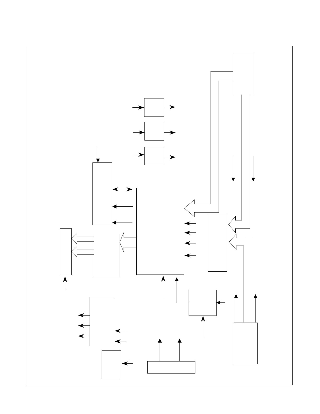
BLOCK DIAGRAM
- 10 -
D-SUB
DVI-I
Gm5020
including
(ADC / TMDS Rx )
LVDS
(LVDS823)
Memory
(KM416S102BT)
H-Sync A
V-Sync A
Micom
68HC08-BD48
M-CLK
Out - CLK
DE ,H/V Sync out
R,G,B Even/Odd
LCD Module
R,G,B
differential
LVDS:Low Voltage Differential Signaling
Data 48 Bit
Address
Inverte r CTL
Module CTL
R,G,B
Inverter
Digital Signal
3.3V
Reg.
DVDD 3 .3 V
AVD D 3 .3 V
12V
Powe r CTL
V-Sync
ADC CLK
5V
2.5V
Reg.
DVDD2.5V
AVDD2.5V
3.3V
Reg.
PVDD 3 .3 V
3.3 VM
5V 5V
DVI-Analog Signal
R,G,B
H-Sync B
V-Sync B
BA7657
(Video Switch)
R,G,B
5V
H/V-Sync
Hsync
Switch
(A or B)
H-Sync A
H-Sync
H-Sync B
3.3 VM
Power Board
12V
5V
MAIN BOARD
Page 2

DESCRIPTION OF BLOCK DIAGRAM (Main Board)
- 11 -
1. Input signal switching part.
There are two inputs which are analog and digital input.
They come from each 15 pin D-Sub and 24 pin DVI-D connector.
2. Video Controller Part.
This part amplifies the level of video signal for the digital conversion and converts from the analog video signal to
the digital video signal using a pixelclock.
The pixel clock for each mode is generated by the PLL.
The range of the pixel clock is from 25MHz to 135MHz.
This part consists of the Scaler and frame buffers which converts frame rate of input signal to 60Hz frame rate.
The Scaler gets the video signal converted analog to digital, interpolates input to1280 X 1024 resolution signal
and outputs 8-bit R, G, B signal to transmitter.
Especially pre-amp / ADC / Video controller are merged to one chip ‘Gm5020’ by Genesis.
Also FRC is separate.
3. Display Data Transmitter Part.
This part transmit digital signal from the Scaler to the receiver of module.
4. Power Part.
This part consists of the one 5V, two 3.3V and one 2.5 regulators to convert power which is provided 12V, 5V in
Power Board.
12V is provided for inverter, 5V is provided for Micom and LCD Panel.
Also, 5V is converted 3.3V and 2.5V by regulator. Converted power is provided for IC in the main board.
5. MICOM Part.
This part consists of EEPROM IC which stores control data, Reset IC and the Micom.
The Micom distinguishes polarity and frequency of the H/V sync are supplied from signal cable.
The controlled data of each modes is stored in EEPROM.
6. Inverter
The inverter converts from DC12V to AC 700V and operate back-light lamp of module.
Page 3

BLOCK DIAGRAM
- 12 -
EMI
COMPONENTS
LINE
100 ~ 240V
INPUT RECTIFIE R
AND FILTER
ENERGY
TRANSFER
OUTPUT RECTIFIE R
AND FILTER
12V
5V
GND
SIGNAL
COLLENTION
PHOTO-COUPLER
ISOLATION
PWM CONTROL
CIRCUIT
HVDC
100KHz
PRIMARY
SECONDARY
50 ~ 60Hz
POWER BOADR
DESCRIPTION OF BLOCK DIAGRAM
1. EMI components.
This part contains of EMI components to comply with global marketing EMI standards like FCC, VCCI CISPR,
the circuit included a line-filter, across line capacitor and of course the primary protection fuse.
2. Input rectifier and filter.
This part function is for transfer the input AC voltage to a DC voltage through a bridge rectifier and a bulk capacitor.
3. Energy Transfer.
This part function is transfer the primary energy to secondary through a power transformer.
4. Output rectifier and filter.
This part function is to make a pulse width modulation control and to provide the driver signal to power switch, to
adjust the duty cycle during different AC input and output loading condition to achive the dc output stablize, and also
the over power protection is also monitor by this part.
5. Photo-Coupler isolation.
This part function is to feed back the dc output changing status through a photo transistor to primary controller to
achive the stablized dc output voltage.
6. Signal collection.
This part function is to collect the any change from the dc output and feed back to the primary through photo
transistor
 Loading...