

Page 1
- 9 -
BLOCK DIAGRAM
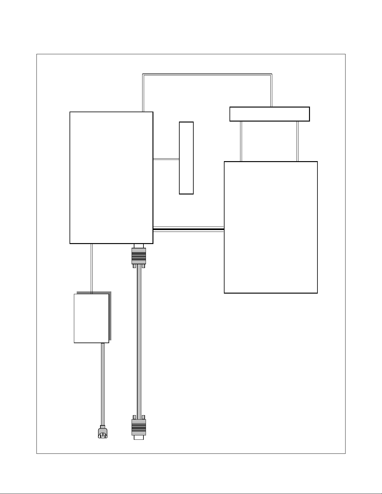
POWER CORD
15-pin D-SUB SIGNAL CABLE
POWER
SUPPLY
CONTROL PCB
INVERTER PCB
MAIN LOGIC
PCB
LCD MODULE
System Block Diagram
Page 2
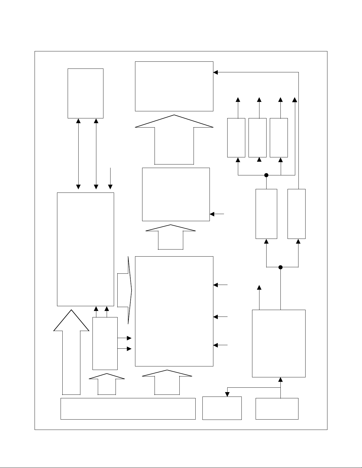
BLOCK DIAGRAM
- 10 -
DC/DC
Converter
(L4973)
24V
ST5V
5V
EEPROM
24LC16
ADC/PLL/Scaler
(gmZAN1)
(MICOM)
(MYS212M)
Switch
FDC6325L
Switch
FDC6325L
Schmitt Trigger
(74HCT14)
LCD
Interface
21Pin
Connector
RGB
H.V
D-
Sub
15P
DDC
Control
DC
Jack
SCL
SDA
TMDS/
Control
CON
9P
Inverter
3.3VD
3.3V_PL
Module Power 5V
3.3V_P
L
3.3VD
ST5V
Transmitter
sil100
RGB
+3.3V
3.3V_AD
Regulator
BA033
Regulator
BA033
Regulator
BA033
3.3V_A
D
+3.3V
Page 3

DESCRIPTION OF BLOCK DIAGRAM
- 11 -
1. Scaler One chip IC(GMZAN1, U3)
GMZAN1 (U3) is one chip IC which it supports four internal function blocks of Video Amp, PLL, A/D converter and
Video processor.
Video signal (0.7Vp.p) clamped through C44, 45, 191 with matching IC’s proper cut off voltage.
This signal is processed as a proper 8 bit digital signal by U3’s amplifying, phase locking, A/D converting,
and scaling operations.
U3 generates Clock, Horizontal and Vertical sync, Data Enable signals as LCD Panel’s input signals.
2. System Controller (Microprocessor) Circuit
1) Microprocessor (U4) distinguishes polarity and frequency by calculating horizontal and vertical sync input
from signal source.
2) Microprocessor (U4) carries out power control by sending power-down trigger signal to each IC.
3) Microprocessor (U4) communicates with EEPROM (U1), and GMZAN1 (U3) through IIC(2 lines) or 6 bit bus line.
It makes all devices operated properly.
4) Microprocessor (U4) let User adjust screen by OSD function.
3. DC/ DC Converter
This circuit supplies DC power for each device needing DC voltage of 3.3VD, 3.3V_AD, 3.3V_PL, and 5VS.
L4973D5.1(U13) , the DC/DC controller IC converts input 12Vdc into 5VS and 3.3Vdc with peripheral circuit
composed of Inductor (L11), condensing components (ZD5, C72), and Regulators(U2, U7, U24).
MODPWR(3.3V) for LCD module power is switched by U12, switching FET, controlled by Microprocessor.
3.3VD, 3.3V_AD, and 3.3V_PL for GMZAN1 (U3) is switched by U5, switching FET, controlled by Microprocessor for
Power saving.
4. Transmitter
Transmitter (U9) gets signals of HSYNC , VSYNC, DEN, DCLK from U3, and outputs TMDS
(Transition Minimized Differential Signal) through TX pins.
When PD pin’s input is low, transmitter goes to power down mode.
 Loading...