

Page 1
Internal Use Only
North/Latin America http://aic.lgservice.com
Europe/Africa http://eic.lgservice.com
Asia/Oceania http://biz.lgservice.com
LED LCD TV
SERVICE MANUAL
CHASSIS : LA23E
MODEL : 55LM9600 55LM9600-UC
CAUTION
BEFORE SERVICING THE CHASSIS,
READ THE SAFETY PRECAUTIONS IN THIS MANUAL.
Printed in KoreaP/NO : MFL67460305 (1204-REV00)
Page 2

CONTENTS
CONTENTS .............................................................................................. 2
PRODUCT SAFETY ................................................................................. 3
SPECIFICATION ....................................................................................... 4
ADJUSTMENT INSTRUCTION .............................................................. 10
EXPLODED VIEW .................................................................................. 18
SCHEMATIC CIRCUIT DIAGRAM ..............................................................
Only for training and service purposes
- 2 -
LGE Internal Use OnlyCopyright © LG Electronics. Inc. All rights reserved.
Page 3
SAFETY PRECAUTIONS
IMPORTANT SAFETY NOTICE
Many electrical and mechanical parts in this chassis have special safety-related characteristics. These parts are identified by in the
Schematic Diagram and Exploded View.
It is essential that these special safety parts should be replaced with the same components as recommended in this manual to prevent
Shock, Fire, or other Hazards.
Do not modify the original design without permission of manufacturer.
General Guidance
An isolation Transformer should always be used during the
servicing of a receiver whose chassis is not isolated from the AC
power line. Use a transformer of adequate power rating as this
protects the technician from accidents resulting in personal injury
from electrical shocks.
It will also protect the receiver and it's components from being
damaged by accidental shorts of th e cir cuitry that may be
inadvertently introduced during the service operation.
If any fuse (or Fusible Resistor) in this TV receiver is blown,
replace it with the specified.
When replacing a high wattage resistor (Oxide Metal Film Resistor,
over 1 W), keep the resistor 10 mm away from PCB.
Keep wires away from high voltage or high temperature parts.
Before returning the receiver to the customer,
always perform an AC leakage current check on the exposed
metallic parts of the cabinet, such as antennas, terminals, etc., to
be sure the set is safe to operate without damage of electrical
shock.
Leakage Current Cold Check(Antenna Cold Check)
With the instrument AC plug removed from AC source, connect an
electrical jumper across the two AC plug prongs. Place the AC
switch in the on position, connect one lead of ohm-meter to the AC
plug prongs tied together and touch other ohm-meter lead in turn to
each exposed metallic parts such as antenna terminals, phone
jacks, etc.
If the exposed metallic part has a return path to the chassis, the
measured resistance should be between 1 MΩ and 5.2 MΩ.
When the exposed metal has no return path to the chassis the
reading must be infinite.
An other abnormality exists that must be corrected before the
receiver is returned to the customer.
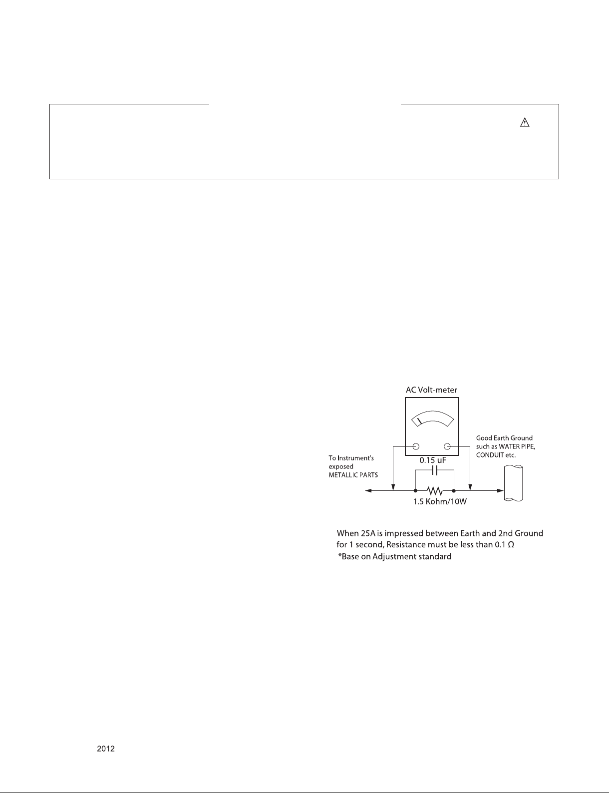
Leakage Current Hot Check (See below Figure)
Plug the AC cord directly into the AC outlet.
Do not use a line Isolation Transformer during this check.
Connect 1.5 K / 10 watt resistor in parallel with a 0.15 uF capacitor
between a known good earth ground (Water Pipe, Conduit, etc.)
and the exposed metallic parts.
Measure the AC voltage across the resistor using AC voltmeter
with 1000 ohms/volt or more sensitivity.
Reverse plug the AC cord into the AC outlet and repeat AC voltage
measurements for each exp ose d metallic par t. Any voltage
measured must not exceed 0.75 volt RMS which is corresponds to
0.5 mA.
In case any measurement is out of the limits specified, there is
possibility of shock hazard and the set must be checked and
repaired before it is returned to the customer.
Leakage Current Hot Check circuit
Only for training and service purposes
- 3 -
LGE Internal Use OnlyCopyright © LG Electronics. Inc. All rights reserved.
Page 4
SPECIFICATION
NOTE : Specifications and others are subject to change without notice for improvement
1. Application range
This spec sheet is applied LCD TV with ( LA23E ) chassis
2. Test condition
Each part is tested as below without special notice.
1)
Temperature : 25
2) Relative Humidity: 65 % ± 10 %
3) Power Voltage : Standard input voltage
(220~240V@ 60Hz)
4) Specification and performance of each parts are followed
ea ch drawing and s pe cificatio n b y p art number in
accordance with BOM.
5) The receiver must be operated for about 20 minutes prior to
the adjustment.
3. Test method
1) Performance: LGE TV test method followed
2) Demanded other specification
- Safety : UL, CSA, CE, IEC specification
- EMC: FCC, ICES, CE, IEC specification
- Wireless : WirelessHD Specification (Option)
ºC
± 5 ºC (77±9 ºF), CST : 40±5
ºC
.
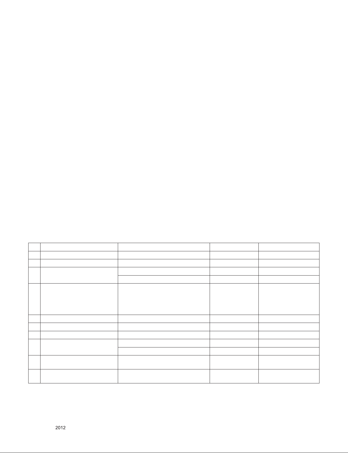
4. General Specification
No Item Specication Remark
1 Market 1) North America
2 Broadcasting System 1) ATSC / NTSC
3 Receiving System 1) VSB/64 & 256 QAM/ NTSC-M
4 Input Voltage AC 100 ~ 240V 50/60Hz FHD + T120Hz
5 Available Channel 1) VHF : 02~13
2) UHF : 14~69
3) DTV : 02-69
4) CATV : 01~135
5) CADTV : 01~135
6 Screen Size 47/55 inche Wide(1920 × 1080) 47/55LM9600-UC
7 Aspect Ratio 16:9
8 Tuning System FS
9 LCD Module LC470DUT-SEF1 LGD 47LM9600-UC
LC550DUT-SEF1 LGD 55LM9600-UC
10 Operating Environment 1) Temp : 0 ~ 40 deg
2) Humidity : ~ 80 %
11 Storage Environment 1) Temp : -20 ~ 60 deg
2) Humidity : ~ 85 %
Only for training and service purposes
- 4 -
LGE Internal Use OnlyCopyright © LG Electronics. Inc. All rights reserved.
Page 5
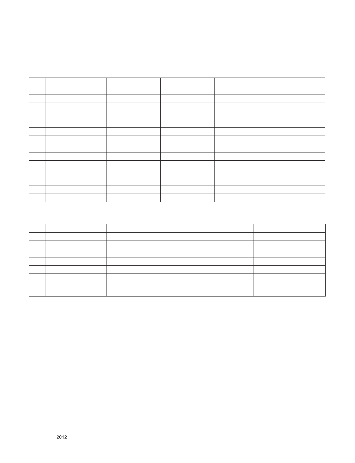
5. External input format
5.1. 2D mode
5.1.1. Component input (Y, CB/PB, CR/PR)
No. Resolution H-freq(kHz) V-freq.(kHz) Pixel clock Proposed
1. 720*480 15.73 60.00 13.5135 SDTV ,DVD 480I
2. 720*480 15.73 59.94 13.50 SDTV ,DVD 480I
3. 720*480 31.50 60.00 27.027 SDTV 480P
4. 720*480 31.47 59.94 27.00 SDTV 480P
5. 1280*720 45.00 60.00 74.25 HDTV 720P
6. 1280*720 44.96 59.94 74.176 HDTV 720P
7. 1920*1080 33.75 60.00 74.25 HDTV 1080I
8. 1920*1080 33.72 59.94 74.176 HDTV 1080I
9. 1920*1080 67.50 60.00 148.50 HDTV 1080P
10. 1920*1080 67.432 59.94 148.352 HDTV 1080P
11. 1920*1080 27.00 24.00 74.25 HDTV 1080P
12. 1920*1080 26.97 23.94 74.176 HDTV 1080P
13. 1920*1080 33.75 30.00 74.25 HDTV 1080P
14. 1920*1080 33.71 29.97 74.176 HDTV 1080P
5.1.2. RGB Input (PC)
No. Resolution H-freq(kHz) V-freq.(kHz) Pixel clock Proposed
1 640*350 31.468 70.09 25.17 EGA Х
2 720*400 31.469 70.08 28.32 DOS O
3 640*480 31.469 59.94 25.17 VESA(VGA) O
4 800*600 37.879 60.31 40.00 VESA(SVGA) O
5 1024*768 48.363 60.00 65.00 VESA(XGA) O
6 1360*768 47.712 60.015 85.50 VESA (WXGA) Х
7 1920*1080 67.5 60 148.8 WUXGA
(Reduced Blanking)
O
Only for training and service purposes
- 5 -
LGE Internal Use OnlyCopyright © LG Electronics. Inc. All rights reserved.
Page 6
5.1.3. HDMI Input 1 (PC/DTV)
No Resolution H-freq(kHz) V-freq.(Hz) Pixel clock(MHz) Proposed
HDMI-PC
1 31.468 70.09 25.17 25.17 EGA Х
2 31.469 70.08 28.32 28.32 DOS O
3 31.469 59.94 25.17 25.17 VESA(VGA) O
4 37.879 60.31 40.00 40.00 VESA(SVGA) O
5 48.363 60.00 65.00 65.00 VESA(XGA) O
6 54.348 60.053 80.00 85.50 VESA O
7 63.981 60.020 108.00 108.00 VESA (SXGA) O
8 47.712 60.015 85.50 148.5 VESA (WXGA) O
9 1920*1080 67.5 60 148.5
HDMI-DTV
1 720*480 31.50 60.00 27.027 SDTV 480P
2 720*480 31.47 59.94 27.00 SDTV 480P
3 1280*720 45.00 60.00 74.25 HDTV 720P
4 1280*720 44.96 59.94 74.176 HDTV 720P
5 1920*1080 33.75 60.00 74.25 HDTV 1080I
6 1920*1080 33.72 59.94 74.176 HDTV 1080I
7 1920*1080 67.50 60.00 148.50 HDTV 1080P
8 1920*1080 67.432 59.94 148.352 HDTV 1080P
9 1920*1080 27.00 24.00 74.25 HDTV 1080P
10 1920*1080 26.97 23.976 74.176 HDTV 1080P
11 1920*1080 33.75 30.00 74.25 HDTV 1080P
12 1920*1080 33.71 29.97 74.176 HDTV 1080P
WUXGA(Reduced Blanking)
O
Only for training and service purposes
- 6 -
LGE Internal Use OnlyCopyright © LG Electronics. Inc. All rights reserved.
Page 7
5.2. 3D mode
5.2.1. RF Input
No Resolution H-freq(kHz) V-freq.(Hz) Pixel clock(MHz) Proposed Remark
1 1920*1080 45 60 74.25 HDTV 1080I Side by Side (Half), Top & Bottom
2 1280*720 45 60 74.25 HDTV 720P Side by Side (Half), Top & Bottom
5.2.2. USB Input (3D supported mode automatically)
No Resolution H-freq(kHz) V-freq.(Hz) Pixel clock(MHz) Proposed Remark
1 1920*1080 33.75 30.00 74.25 HDTV 1080p Side by Side (Half), Top & Bottom,
Checkerboard, MPO (Photo)
5.2.3. USB Input (3D supported mode manually)
No Resolution H-freq(kHz) V-freq.(Hz) Pixel clock(MHz) Proposed Remark
1 1920*1080 33.75 30.00 74.25 HDTV 1080p Side by Side (Half), Top & Bottom
Checkerboard, Single Frame
Sequential,
Row Interleaving, Column Interleaving
(Photo : Side by Side, Top & Bottom)
5.2.4. HDMI-PC Input (3D supported mode manually)
No Resolution H-freq(kHz) V-freq.(Hz) Pixel clock(MHz) Remark
1 1024*768 48.363 60.004 65.000 Side by Side (Half), Top & Bottom
2 1360*768 47.712 60.015 85.500 Side by Side (Half), Top & Bottom
3 1920*1080 67.50 60.00 148.50 Side by Side (Half), Top & Bottom
Checkerboard, Single Frame Sequential
Row Interleaving, Column Interleaving
5.2.5. RGB-PC Input
No Resolution H-freq(kHz) V-freq.(Hz) Pixel clock(MHz) Remark
1 1920*1080 67.5 60.000 148.5 Side by Side (Half) , Top & Bottom
2 1360*768 47.712 60.015 85.50 Side by Side (Half) , Top & Bottom
3 1024*768 48.363 60.00 65.00 Side by Side (Half) , Top & Bottom
5.2.6. HDMI 1.3(3D supported mode manually)
No Resolution H-freq(kHz) V-freq.(Hz) Pixel clock(MHz) Remark
1 1280*720p 45.00 60.00 74.25 Side by Side (Half) , Top & Bottom,
Single Frame Sequential
2 1920*1080i 33.75 60.00 74.25 Side by Side (Half) , Top & Bottom
3 1920*1080p 67.50 60.00 148.50 Side by Side (Half) , Top & Bottom
Checkerboard, Single Frame Sequential
Row Interleaving, Column Interleaving
4 1920*1080p 27.00 24.000 74.25 Side by Side (Half) , Top & Bottom
Checkerboard
5 1920*1080p 33.75 30.000 74.25 Side by Side (Half), Top & Bottom
Checkerboard
Only for training and service purposes
- 7 -
LGE Internal Use OnlyCopyright © LG Electronics. Inc. All rights reserved.
Page 8
5.2.7. HDMI 1.4a(3D supported mode automatically)
No Resolution H-freq(kHz) V-freq.(Hz) Pixel clock(MHz) Proposed Remark
1 1280*720p 89.91 / 90.00 59.94 / 60.00 148.35 / 148.50 Mandatory Frame Packing,
2 1280*720p 44.96 / 45.00 59.94 / 60.00 74.18 / 74.25 Mandatory Top & Bottom
3 1920*1080i 33.72 / 33.75 59.94 / 60.00 74.18 / 74.25 Mandatory Side by Side (Half)
4 1920*1080p 43.94 / 54.00 23.97 / 24.00 148.35 / 148.50 Mandatory Frame Packing,
5 1920*1080p 26.97 / 27.00 23.97 / 24.00 74.18 / 74.25 Mandatory Top & Bottom
6 1280*720p 44.96 / 45.00 59.94 / 60.00 74.18 / 74.25 Primary Side by Side (Half)
7 1920*1080i 67.432 / 67.50 59.94 / 60.00 148.35 / 148.50 Primary Frame Packing
8 1920*1080p 67.43 / 67.50 59.94 / 60.00 148.35 / 148.50 Primary Top & Bottom
9 1920*1080p 26.97 / 27.00 23.97 / 24.00 74.18 / 74.25 Primary Side by Side (Half)
10 1920*1080p 67.432 / 67.50 29.976 / 30.00 148.35 / 148.50 Primary Frame Packing,
11 1920*1080p 33.716 / 33.75 29.976 / 30.00 74.18 / 74.25 Primary Top & Bottom
12 1920*1080i 33.72 / 33.75 59.94 / 60.00 74.18 / 74.25 Secondary Top & Bottom
13 1920*1080p 67.43 / 67.50 59.94 / 60.00 148.35 / 148.50 Secondary Side by Side (Half)
14 1920*1080p 33.716 / 33.75 29.976 / 30.00 74.18 / 74.25 Secondary Side by Side (Half)
15 720*480p 62.938 / 63.00 59.94 / 60.00 54.00 / 54.054 Secondary (16:9) Frame Packing,
16 720*480p 31.469 / 31.50 59.94 / 60.00 27.00 / 27.027 Secondary (16:9) Top & Bottom
17 720*480p 31.469 / 31.50 59.94 / 60.00 27.00 / 27.027 Secondary (16:9) Side by Side (Half)
18 720*480p 62.938 / 63.00 59.94 / 60.00 54.00 / 54.054 Secondary (4:3) Frame Packing,
19 720*480p 31.469 / 31.50 59.94 / 60.00 27.00 / 27.027 Secondary (4:3) Top & Bottom
20 720*480p 31.469 / 31.50 59.94 / 60.00 27.00 / 27.027 Secondary (4:3) Side by Side (Half)
21 640*480p 62.938 / 63.00 59.94 / 60.00 50.35 / 50.40 Secondary Frame Packing,
22 640*480p 31.469 / 31.50 59.94 / 60.00 25.175 / 25.20 Secondary Top & Bottom
23 640*480p 31.469 / 31.50 59.94 / 60.00 25.175 / 25.20 Secondary Side by Side (Half)
24 1280*720p 89.91 / 90.00 59.94 / 60.00 148.35 / 148.50 Line Alternative
25 1280*720p 44.96 / 45.00 59.94 / 60.00 148.35 / 148.50 Side by Side (Full)
26 1920*1080i 67.432 / 67.50 59.94 / 60.00 148.35 / 148.50 Field Alternative
27 1920*1080i 33.72 / 33.75 59.94 / 60.00 148.35 / 148.50 Side by Side (Full)
28 1920*1080p 43.94 / 54.00 23.97 / 24.000 148.35 / 148.50 Line Alternative
29 1920*1080p 26.97 / 27.00 23.97 / 24.000 148.35 / 148.50 Side by Side (Full)
30 1920*1080p 67.432 / 67.50 29.976 / 30.00 148.35 / 148.50 Line Alternative
31 1920*1080p 33.716 / 33.75 29.976 / 30.00 148.35 / 148.50 Side by Side (Full)
32 720*480p 62.938 / 63.00 59.94 / 60.00 54.00 / 54.054 16:9 Line Alternative
33 720*480p 31.469 / 31.50 59.94 / 60.00 54.00 / 54.054 16:9 Side by Side (Full)
34 720*480p 62.938 / 63.00 59.94 / 60.00 54.00 / 54.054 4:3 Line Alternative
35 720*480p 31.469 / 31.50 59.94 / 60.00 54.00 / 54.054 4:3 Side by Side (Full)
36 640*480p 62.938 / 63.00 59.94 / 60.00 50.35 / 50.40 Line Alternative
37 640*480p 31.469 / 31.50 59.94 / 60.00 50.35 / 50.40 Side by Side (Full)
Only for training and service purposes
- 8 -
LGE Internal Use OnlyCopyright © LG Electronics. Inc. All rights reserved.
Page 9
R
L
R
L
5.2.8. DLNA Input (3D supported mode automatically)
No Resolution H-freq(kHz) V-freq.(Hz) Pixel clock(MHz) Proposed Remark
1 1920*1080 33.75 30.00 74.25 HDTV 1080p Side by Side (Half), Top & Bottom,
Checkerboard, MPO (Photo)
5.2.9. DLNA Input (3D supported mode manually)
No Resolution H-freq(kHz) V-freq.(Hz) Pixel clock(MHz) Proposed Remark
1 1920*1080 33.75 30.00 74.25 HDTV 1080p Side by Side (Half), Top & Bottom
Checkerboard, Single Frame
Sequential,
Row Interleaving, Column Interleaving
(Photo : Side by Side, Top & Bottom)
5.2.10. Component Input
No Resolution H-freq(kHz) V-freq.(Hz) Pixel clock(MHz) Proposed Remark
1 1280*720 44.96 59.94 74.176 HDTV 720P Side by Side, Top & Bottom
2 1920*1080 33.75 60.00 74.25 HDTV 1080I Side by Side, Top & Bottom
3 1920*1080 33.72 59.94 74.176 HDTV 1080I Side by Side, Top & Bottom
4 1920*1080 67.500 60 148.50 HDTV 1080P Side by Side, Top & Bottom
5 1920*1080 67.432 59.94 148.352 HDTV 1080P Side by Side, Top & Bottom
6 1920*1080 27.000 24.000 74.25 HDTV 1080P Side by Side, Top & Bottom
7 1920*1080 26.97 23.976 74.176 HDTV 1080P Side by Side, Top & Bottom
8 1920*1080 33.75 30.000 74.25 HDTV 1080P Side by Side, Top & Bottom
9 1920*1080 33.71 29.97 74.176 HDTV 1080P Side by Side, Top & Bottom
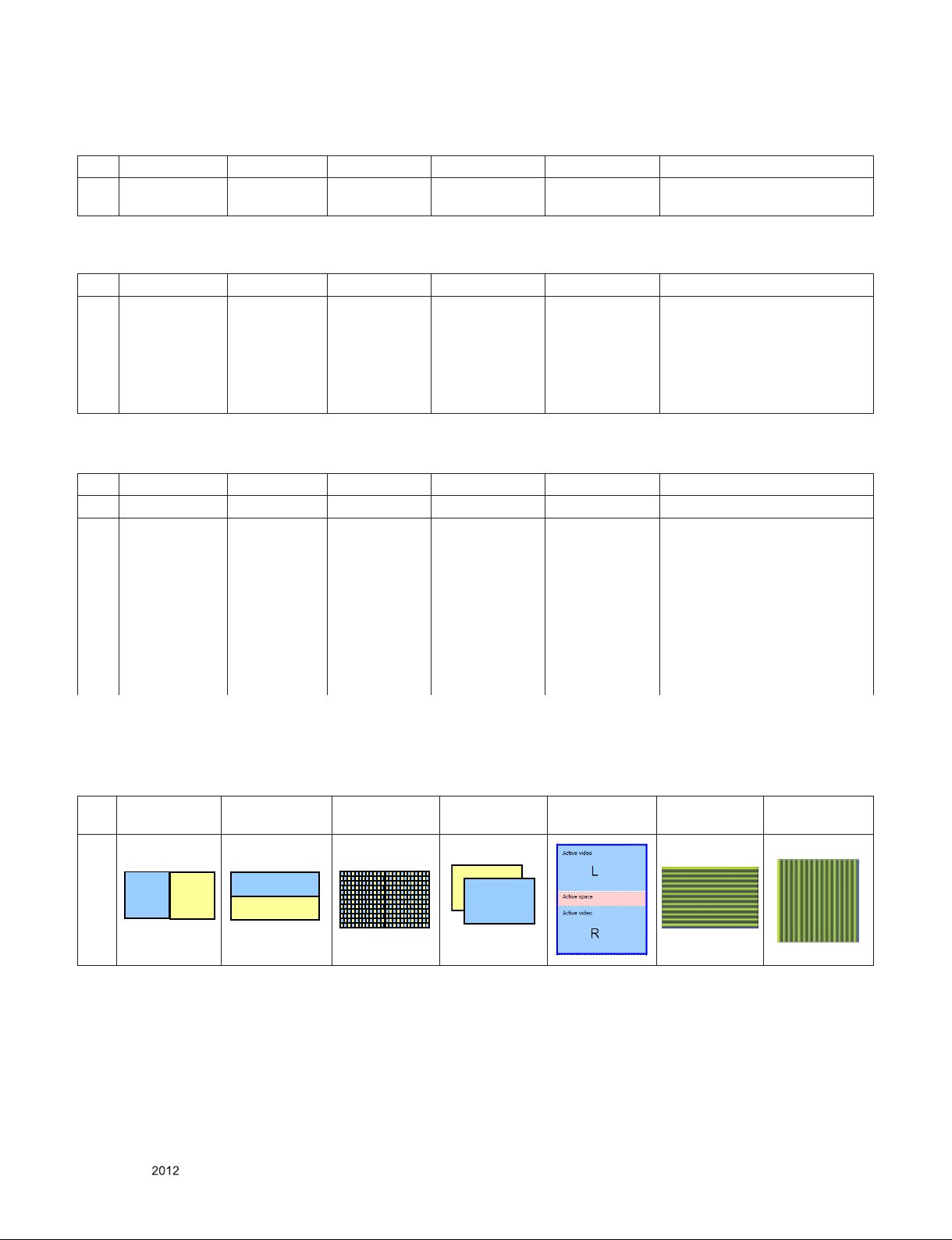
5.3. 2D to 3D Mode
- Remark: 3D Input mode
No. Side by Side Top & Bottom Checkerboard Single Frame
Sequential
1
- 9 -
Only for training and service purposes
Frame Packing Line
Interleaving
Column
Interleaving
LGE Internal Use OnlyCopyright © LG Electronics. Inc. All rights reserved.
Page 10
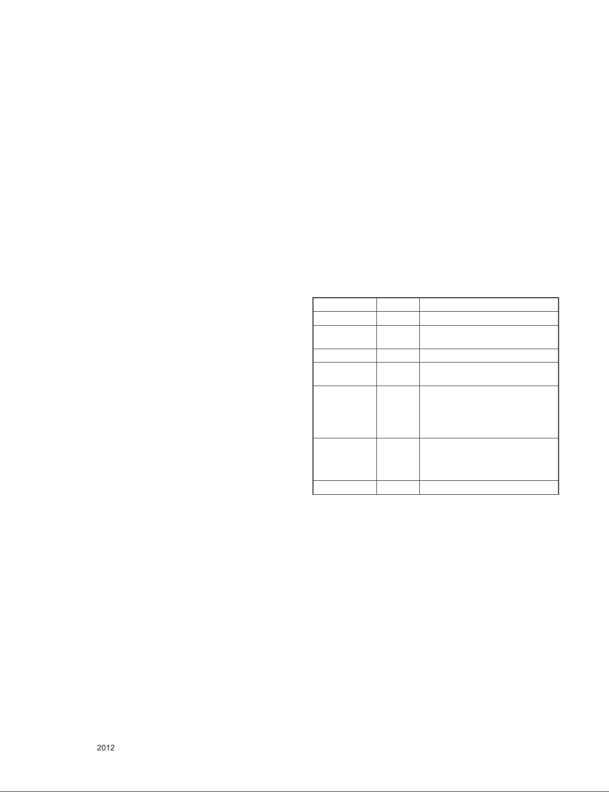
ADJUSTMENT INSTRUCTION
1. Application Range
This spec. sheet applies to LA23E/J Chassis applied LCD TV
all models manufactured in TV factory
2. Specification
(1) Because this is not a hot chassis, it is not necessary to use
an isolation transformer. However, the use of isolation
transformer will help protect test instrument.
(2) Adjustment must be done in the correct order.
(3) The adjustment must be performed in the circumstance of
25 ±5 °C of temperature and 65±10% of relative humidity if
there is no specific designation.
(4) The input voltage of the receiver must keep 100~240V,
50/60Hz.
(5) The receiver must be operated for about 5 minutes prior to
the adjustment when module is in the circumstance of over
15 °C
In case of keeping module is in the circumstance of 0°C, it
should be placed in the circumstance of above 15°C for 2
hours
In case of keeping module is in the circumstance of below
-20°C, it should be placed in the circumstance of above
15°C for 3 hours.
[Caution]
When still image is displayed for a period of 20 minutes or
longer (especially where W/B scale is strong.
Digital pattern 13ch and/or Cross hatch pattern 09ch), there
can some afterimage in the black level area
3.3. Automatic Adjustment
3.3.1. Overview
ADC adjustment is needed to find the optimum black level and
gain in Analog-to-Digital device and to compensate RGB
deviation
3.3.2. Equipment & Condition
1) Jig (RS-232C protocol)
2) Inner Pattern
- Resolution : 1080p (Inner Pattern)
- Resolution : 1024*768 RGB (Inner Pattern)
- Pattern : Horizontal 100% Color Bar Pattern
- Pattern level : 0.7±0.1 Vp-p
3.3.3 Adjustment
3.3.3.1. Adjustment method
▪ Using RS-232, adjust items listed in 3.1 in the other shown in
“4.1.3.3”
3.3.3.2. Adj. protocol
Protocol Command Set ACK
Enter adj. mode aa 00 00 a 00 OK00x
Source change xb 00 40
xb 00 60
Begin adj. ad 00 10
Return adj. result OKx (Case of Success)
Read adj. data (main)
ad 00 20
b 00 OK40x (Adjust 480i Comp1 )
b 00 OK60x (Adjust 1024*768 RGB)
NGx (Case of Fail)
(main)
000000000000000000000000007c007b006dx
3. Adjustment items
3.1. Final assembly adjustment
▪ EDID/DDC check
▪ White Balance adjustment
▪ ADC Adjustment check
▪ RS-232C functionality check
▪ Factory Option setting per destination
▪ Ship-out mode setting (In-Stop)
3.2. Etc
▪ Ship-out mode
▪ Tool option menu
▪ USB Download(S/W Update, Option, Service only)
(sub )
ad 00 21
Conrm adj. ad 00 99 NG 03 00x (Fail)
End adj. aa 00 90 a 00 OK90x
3.3.3.3 Adj. order
▪ aa 00 00 [Enter ADC adj. mode]
▪ xb 00 40 [Change input source to Component1(480i)]
▪ ad 00 10 [Adjust 480i Comp1]
▪ xb 00 60 [Change input source to RGB(1024*768)]
▪ ad 00 10 [Adjust 1024*768 RGB]
▪ ad 00 90 End adj.
Ref) ADC adj. RS232C Protocol_Ver1.0
(Sub)
000000070000000000000000007c00830077x
NG 03 01x (Fail)
NG 03 02x (Fail)
OK 03 03x (Success)
Only for training and service purposes
- 10 -
LGE Internal Use OnlyCopyright © LG Electronics. Inc. All rights reserved.
Page 11
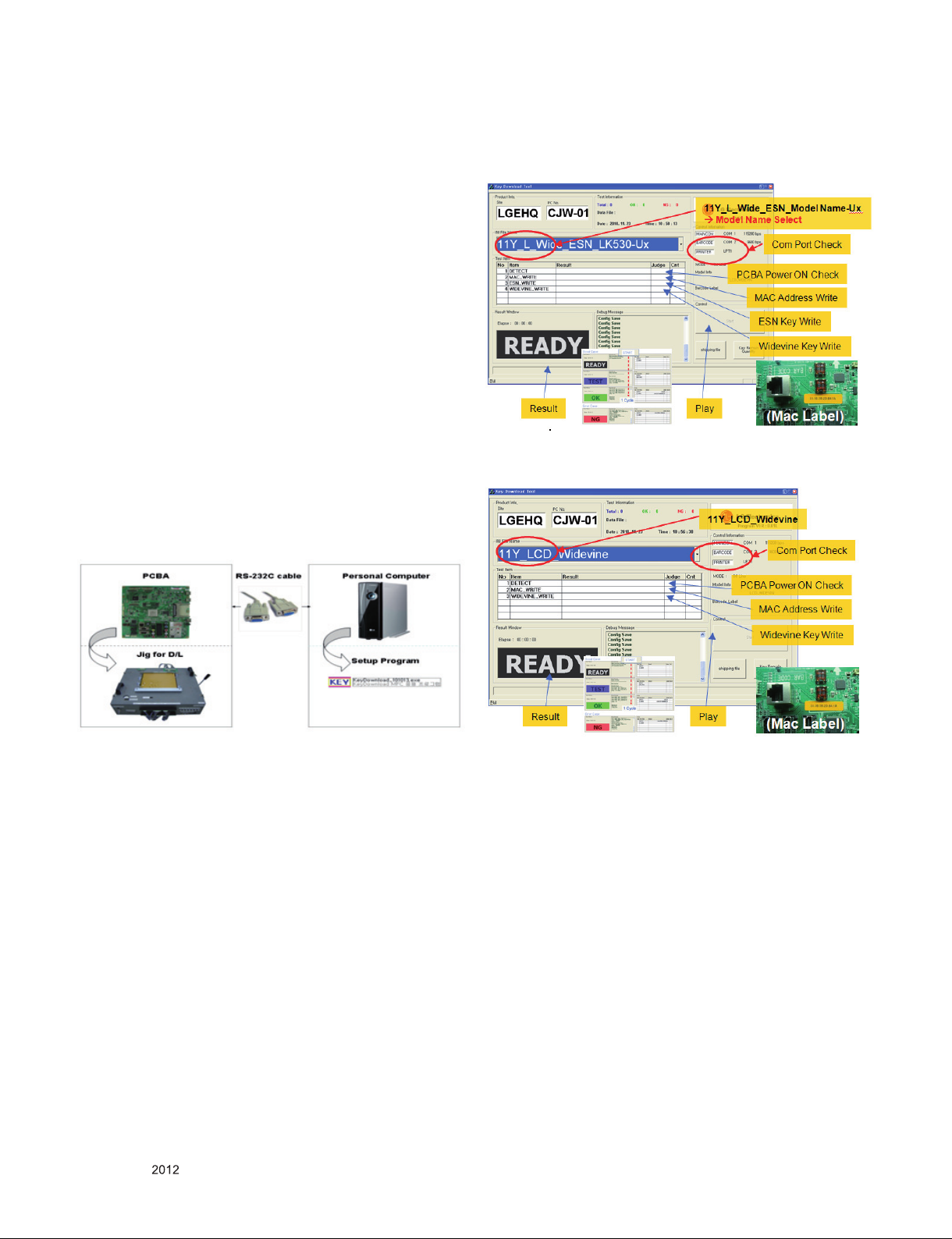
4. Manual Adjustment
4.1. MAC Address, ESN Key and Widevine
Key download
4.1.1. Equipment & Condition
1) Play file: keydownload.exe
4.1.2. Communication Port connection
1) Key Write: Com 1,2,3,4 and 115200 (Baudrate)
2) Barcode: Com 1,2,3,4 and 9600 (Baudrate)
4.1.3. Download process
1) Select the download items.
2) Mode check: Online Only
3) Check the test process
- U S, Canad a m ode ls : DET EC T -> M AC _WR IT E ->
WIDEVINE_WRITE
- Korea, Me xico models: DE TECT -> MA C_WRITE ->
WIDEVINE_WRITE
4) Play : START
5) Check of result: Ready, Test, OK or NG
6) Printer out (MAC Address Label)
4.1.4. Communication Port connection
1) Connect: PCBA Jig -> RS-232C Port == PC -> RS-232C
Port
4.1.5. Download
1) US, Canada, Mexico models (12Y LCD TV + MAC +
Widevine + ESN Key)
2) Korea, Mexico models (11Y LCD TV + MAC + Widevine
Only)
Only for training and service purposes
4.1.6. Inspection
- In INSTART menu, check these keys.
- 11 -
LGE Internal Use OnlyCopyright © LG Electronics. Inc. All rights reserved.
Page 12
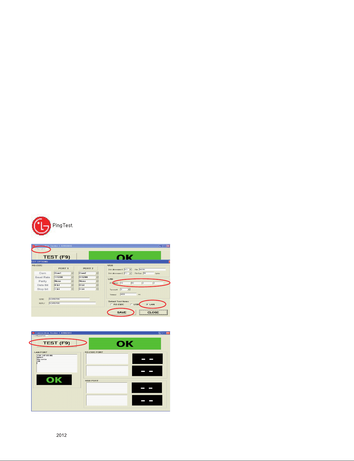
4.2. PING Test
* LAN card can be verified by using PING test
4.2.1 Adjustment Method(Board)
(1) Connect LAN to the board and power on.
(Default IP can be set to automatic setting. When power
ON, IP can be automatically be achieved from the router)
(2) Press ADJ key in the adjustment remote control.
(3) Check Network status by pressing 13. ACAP PING TEST
in EZ ADJUST. If it operates properly, it will show “Network
is operating properly.” If it does not, it will show “Network is
not working properly.”
4.2.2 Adjustment Method(Manufacturer)
(4) Connect the PC with PING Test program installed and the
LAN port of the SET via Cross LAN Cable. (The IP setting
of the PC has to be 12.12.2.3)
(5) After the PING Test program has been executed, check the
program setting. (IP of the set will be 12.12.2.2. Double
check the setting. Do not check the Modem because it will
not be used.)
(6) Press the Power Only Key in Adjustment remote control.
(IP of the set will be set)
(7) Upon pressing “RUN” in the program, it will show “OK” or
“NG” according to the test result.
● After all the adjustments, to disable the IP setting, press
INSTOP key.
4.3 EDID Download
4.3.1 Overview
▪ It is a VESA regulation. A PC or a MNT will display an optimal
resolution through information sharing without any necessity
of user input. It is a realization of “Plug and Play”.
4.3.2 Equipment
▪ Since embedded EDID data is used, EDID download JIG,
HDMI cable and D-sub cable are not need.
▪ Adjust remocon
4.3.3 Download method
1) Press Adj. key on the Adj. R/C,
2) Select EDID D/L menu.
3) By pressing Enter key, EDID download will begin
4) If Download is successful, OK is display, but If Download is
failure, NG is displayed.
5) If Download is failure, Re-try downloads.
※ Caution) When EDID Download, must remove RGB/HDMI
Cable.
4.3.3.1. EDID DATA
# HDMI 1(C/S : 43 2C)
EDID Block 0, Bytes 0-127 [00H-7FH]
0 1 2 3 4 5 6 7 8 9 A B C D E F
---------------------------------------------------------------------------------------- 0 | 00 FF FF FF FF FF FF 00 1E 6D 01 00 01 01 01 01
10 | 01 16 01 03 80 A0 5A 78 0A EE 91 A3 54 4C 99 26
20 | 0F 50 54 A1 08 00 31 40 45 40 61 40 71 40 81 80
30 | 01 01 01 01 01 01 02 3A 80 18 71 38 2D 40 58 2C
40 | 45 00 A0 5A 00 00 00 1E 66 21 50 B0 51 00 1B 30
50 | 40 70 36 00 A0 5A 00 00 00 1E 00 00 00 FD 00 39
60 | 3F 1F 52 10 00 0A 20 20 20 20 20 20 00 00 00 FC
70 | 00 4C 47 20 54 56 0A 20 20 20 20 20 20 20 01 43
Only for training and service purposes
- 12 -
EDID Block 1, Bytes 128-255 [80H-FFH]
0 1 2 3 4 5 6 7 8 9 A B C D E F
---------------------------------------------------------------------------------------- 0 | 02 03 2E F1 48 90 22 20 05 04 03 02 01 23 09 57
10 | 07 78 03 0C 00 10 00 B8 2D 20 C0 0E 01 4F 00 FE
20 | 08 10 06 10 18 10 28 10 38 10 E3 05 03 01 02 3A
30 | 80 18 71 38 2D 40 58 2C 45 00 A0 5A 00 00 00 1E
40 | 01 1D 80 18 71 1C 16 20 58 2C 25 00 A0 5A 00 00
50 | 00 9E 01 1D 00 72 51 D0 1E 20 6E 28 55 00 A0 5A
60 | 00 00 00 1E 26 36 80 A0 70 38 1F 40 30 20 25 00
70 | A0 5A 00 00 00 1A 00 00 00 00 00 00 00 00 00 2C
LGE Internal Use OnlyCopyright © LG Electronics. Inc. All rights reserved.
Page 13

# HDMI 2(C/S : 43 1C)
EDID Block 0, Bytes 0-127 [00H-7FH]
# HDMI 4(C/S : 43 FC)
EDID Block 0, Bytes 0-127 [00H-7FH]
0 1 2 3 4 5 6 7 8 9 A B C D E F
---------------------------------------------------------------------------------------- 0 | 00 FF FF FF FF FF FF 00 1E 6D 01 00 01 01 01 01
10 | 01 16 01 03 80 A0 5A 78 0A EE 91 A3 54 4C 99 26
20 | 0F 50 54 A1 08 00 31 40 45 40 61 40 71 40 81 80
30 | 01 01 01 01 01 01 02 3A 80 18 71 38 2D 40 58 2C
40 | 45 00 A0 5A 00 00 00 1E 66 21 50 B0 51 00 1B 30
50 | 40 70 36 00 A0 5A 00 00 00 1E 00 00 00 FD 00 39
60 | 3F 1F 52 10 00 0A 20 20 20 20 20 20 00 00 00 FC
70 | 00 4C 47 20 54 56 0A 20 20 20 20 20 20 20 01 43
EDID Block 1, Bytes 128-255 [80H-FFH]
0 1 2 3 4 5 6 7 8 9 A B C D E F
---------------------------------------------------------------------------------------- 0 | 02 03 2E F1 48 90 22 20 05 04 03 02 01 23 09 57
10 | 07 78 03 0C 00 10 00 B8 3D 20 C0 0E 01 4F 00 FE
20 | 08 10 06 10 18 10 28 10 38 10 E3 05 03 01 02 3A
30 | 80 18 71 38 2D 40 58 2C 45 00 A0 5A 00 00 00 1E
40 | 01 1D 80 18 71 1C 16 20 58 2C 25 00 A0 5A 00 00
50 | 00 9E 01 1D 00 72 51 D0 1E 20 6E 28 55 00 A0 5A
60 | 00 00 00 1E 26 36 80 A0 70 38 1F 40 30 20 25 00
70 | A0 5A 00 00 00 1A 00 00 00 00 00 00 00 00 00 1C
# HDMI 3(C/S : 43 0C
EDID Block 0, Bytes 0-127 [00H-7FH]
0 1 2 3 4 5 6 7 8 9 A B C D E F
---------------------------------------------------------------------------------------- 0 | 00 FF FF FF FF FF FF 00 1E 6D 01 00 01 01 01 01
10 | 01 16 01 03 80 A0 5A 78 0A EE 91 A3 54 4C 99 26
20 | 0F 50 54 A1 08 00 31 40 45 40 61 40 71 40 81 80
30 | 01 01 01 01 01 01 02 3A 80 18 71 38 2D 40 58 2C
40 | 45 00 A0 5A 00 00 00 1E 66 21 50 B0 51 00 1B 30
50 | 40 70 36 00 A0 5A 00 00 00 1E 00 00 00 FD 00 39
60 | 3F 1F 52 10 00 0A 20 20 20 20 20 20 00 00 00 FC
70 | 00 4C 47 20 54 56 0A 20 20 20 20 20 20 20 01 43
0 1 2 3 4 5 6 7 8 9 A B C D E F
---------------------------------------------------------------------------------------- 0 | 00 FF FF FF FF FF FF 00 1E 6D 01 00 01 01 01 01
10 | 01 16 01 03 80 A0 5A 78 0A EE 91 A3 54 4C 99 26
20 | 0F 50 54 A1 08 00 31 40 45 40 61 40 71 40 81 80
30 | 01 01 01 01 01 01 02 3A 80 18 71 38 2D 40 58 2C
40 | 45 00 A0 5A 00 00 00 1E 66 21 50 B0 51 00 1B 30
50 | 40 70 36 00 A0 5A 00 00 00 1E 00 00 00 FD 00 39
60 | 3F 1F 52 10 00 0A 20 20 20 20 20 20 00 00 00 FC
70 | 00 4C 47 20 54 56 0A 20 20 20 20 20 20 20 01 43
EDID Block 1, Bytes 128-255 [80H-FFH]
0 1 2 3 4 5 6 7 8 9 A B C D E F
---------------------------------------------------------------------------------------- 0 | 02 03 2E F1 48 90 22 20 05 04 03 02 01 23 09 57
10 | 07 78 03 0C 00 10 00 B8 5D 20 C0 0E 01 4F 00 FE
20 | 08 10 06 10 18 10 28 10 38 10 E3 05 03 01 02 3A
30 | 80 18 71 38 2D 40 58 2C 45 00 A0 5A 00 00 00 1E
40 | 01 1D 80 18 71 1C 16 20 58 2C 25 00 A0 5A 00 00
50 | 00 9E 01 1D 00 72 51 D0 1E 20 6E 28 55 00 A0 5A
60 | 00 00 00 1E 26 36 80 A0 70 38 1F 40 30 20 25 00
70 | A0 5A 00 00 00 1A 00 00 00 00 00 00 00 00 00 FC
# RGB(C/S : 5C)
EDID Block 0, Bytes 0-127 [00H-7FH]
0 1 2 3 4 5 6 7 8 9 A B C D E F
---------------------------------------------------------------------------------------- 0 | 00 FF FF FF FF FF FF 00 1E 6D 01 00 01 01 01 01
10 | 01 16 01 03 68 A0 5A 78 0A EE 91 A3 54 4C 99 26
20 | 0F 50 54 A1 08 00 31 40 45 40 61 40 71 40 81 80
30 | 01 01 01 01 01 01 02 3A 80 18 71 38 2D 40 58 2C
40 | 45 00 A0 5A 00 00 00 1E 66 21 50 B0 51 00 1B 30
50 | 40 70 36 00 A0 5A 00 00 00 1E 00 00 00 FD 00 3A
60 | 3E 1E 53 10 00 0A 20 20 20 20 20 20 00 00 00 FC
70 | 00 4C 47 20 54 56 0A 20 20 20 20 20 20 20 00 5C
EDID Block 1, Bytes 128-255 [80H-FFH]
0 1 2 3 4 5 6 7 8 9 A B C D E F
---------------------------------------------------------------------------------------- 0 | 02 03 2E F1 48 90 22 20 05 04 03 02 01 23 09 57
10 | 07 78 03 0C 00 10 00 B8 4D 20 C0 0E 01 4F 00 FE
20 | 08 10 06 10 18 10 28 10 38 10 E3 05 03 01 02 3A
30 | 80 18 71 38 2D 40 58 2C 45 00 A0 5A 00 00 00 1E
40 | 01 1D 80 18 71 1C 16 20 58 2C 25 00 A0 5A 00 00
50 | 00 9E 01 1D 00 72 51 D0 1E 20 6E 28 55 00 A0 5A
60 | 00 00 00 1E 26 36 80 A0 70 38 1F 40 30 20 25 00
70 | A0 5A 00 00 00 1A 00 00 00 00 00 00 00 00 00 0C
Only for training and service purposes
- 13 -
LGE Internal Use OnlyCopyright © LG Electronics. Inc. All rights reserved.
Page 14
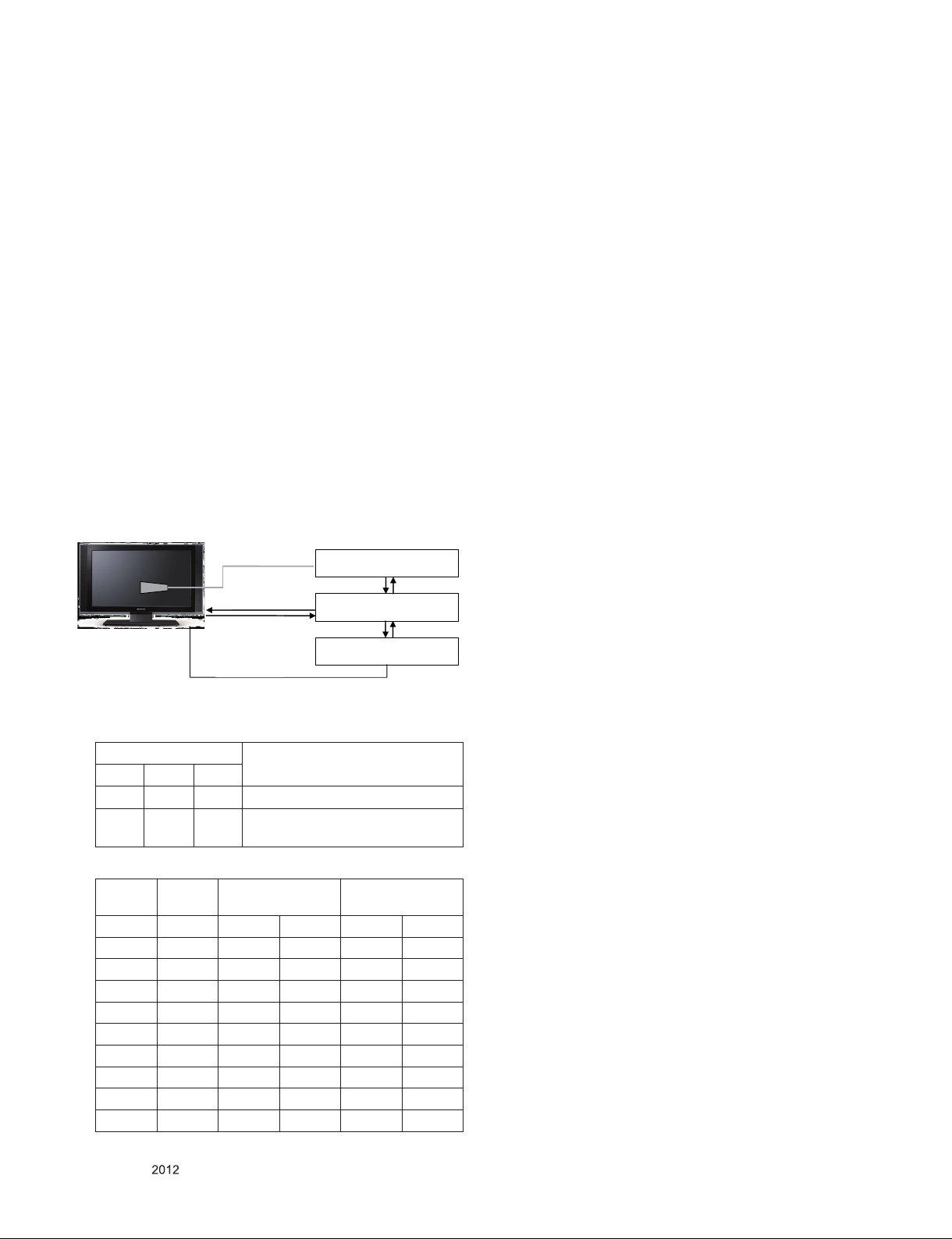
4.4. White Balance Adjustment
If TV internal pattern is used, not needed
4.4.1. Overview
▪ W/B adj. Objective & How-it-works
(1) Objective: To reduce each Panel’s W/B deviation
(2) How-it-works: When R/G/B gain in the OSD is at 192, it
means the panel is at its Full Dynamic Range. In order to
prevent saturation of Full Dynamic range and data, one of
R/G/B is fixed at 192, and the other two is lowered to find
the desired value.
(3) Adj. condition: normal temperature
- Surrounding Temperature: 25±5 °C
- Warm-up time: About 5 Min
- Surrounding Humidity: 20% ~ 80%
4.4.2. Equipment
(1) Color Analyzer: CA-210 (NCG: CH 9 / WCG: CH12 / LED:
CH14)
(2) Adj. Computer (During auto adj., RS-232C protocol is
needed)
(3) Adjust Remocon
(4) Vi deo Signal Generator MSPG-925F 720p/204- Gray
(Model: 217, Pattern: 49)
※ Color Analyzer Matrix should be calibrated using CS-1000
4.4.3. Equipment connection
Color Analyzer
Probe
RS-232C
※
Signal Source
※
4.4.4. Adjustment Command (Protocol)
(1) RS-232C Command used during auto-adj.
RS-232C COMMAND
CMD DATA ID
Wb 00 00 Begin White Balance adj.
Wb 00 ff End White Balance adj.
(internal pattern disappears )
(2) Adjustment Map
Adj. item Command
(lower caseASCII)
CMD1 CMD2 MIN MAX
Cool R Gain j g 00 C0
G Gain j h 00 C0
B Gain j i 00 C0
Medium R Gain j a 00 C0
G Gain j b 00 C0
B Gain j c 00 C0
Warm R Gain j d 00 C0
G Gain j e 00 C0
B Gain j f 00 C0
Explanation
Data Range
(Hex.)
RS-232C
Computer
RS-232C
Pattern Generator
4.4.5. Adj. method
4.4.5.1. Auto adj. method
(1) Set TV in ADJ mode using P-ONLY key (or POWER ON
key)
(2) Place optical probe on the center of the display
- It need to check probe condition of zero calibration before
adjustment.
(3) Connect RS-232C Cable
(4) Select mode in ADJ Program and begin a adjustment.
(5) When WB adjustment is completed with OK message,
check adjustment status of pre-set mode (Cool, Medium,
Warm)
(6) Remove probe and RS-232C cable.
▪ W/B Adj. must begin as start command “wb 00 00” , and
finish as end command “wb 00 ff”, and Adj. offset if need
4.4.5.2. Manual adj. method
(1) Set TV in Adj. mode using POWER ON
(2) Zero Calibrate the probe of Color Analyzer, then place it on
the center of LCD module within 10cm of the surface..
(3) Press ADJ key -> EZ adjust using adj. R/C -> 9. White-
Balance then press the cursor to the right (KEY►). When
KEY(►) is pressed 216 Gray internal pa ttern will be
displayed.
(4) One of R Gain / G Gain / B Gain should be fixed at 192,
and the rest will be lowered to meet the desired value.
(5) Adj. is performed in COOL, MEDIUM, WARM 3 modes of
color temperature.
▪ If internal pattern is not available, use RF input. In EZ Adj.
menu 6.White Balance, you can select one of 2 Test-pattern:
ON, OFF. Default is inner (ON). By selecting OFF, you can
adjust using RF signal in 216 Gray pattern.
▪ Adj. condition and cautionary items
(1) Lighting condition in surrounding area
Surrounding lighting should be lower 10 lux. Try to isolate
adj. area into dark surrounding.
(2) Probe location: Color Analyzer (CA-210) probe should be
within 10cm and perpendicular of the module surface (80°~
100°)
(3) Aging time
- After Aging Sta rt, Keep the Power ON status during 5
Minutes.
- In case of LCD, Back-light on should be checked using no
signal or Full-white pattern.
Only for training and service purposes
- 14 -
LGE Internal Use OnlyCopyright © LG Electronics. Inc. All rights reserved.
Page 15
4.4.6. Reference (White Balance Adj. coordinate and
color temperature)
▪ Luminance: 204 Gray
▪ Standard color coordinate and temperature using CS-1000
(over 26 inch)
Mode
Cool 0.269 0.273 13,000K 0.0000
Medium 0.285 0.293 9,300K 0.0000
Warm 0.313 0.329 6,500K +0.0030
▪
Standard color coordinate and temperature using CA-210(CH 18) - ALEF
Mode
Cool 0.269±0.002 0.273±0.002 13,000K 0.0000
Medium 0.285±0.002 0.293±0.002 9,300K 0.0000
Warm 0.313±0.002 0.329±0.002 6,500K +0.0030
▪
Standard color coordinate and temperature using CA-210(CH 14) - LGD
Mode
Cool 0.269±0.002 0.273±0.002 13,000K 0.0000
Medium 0.285±0.002 0.293±0.002 9,300K 0.0000
Warm 0.313±0.002 0.329±0.002 6,500K 0.0000
Coordinate
X Y
Coordinate
X Y
Coordinate
X Y
Temp △uv
Temp △uv
Temp △uv
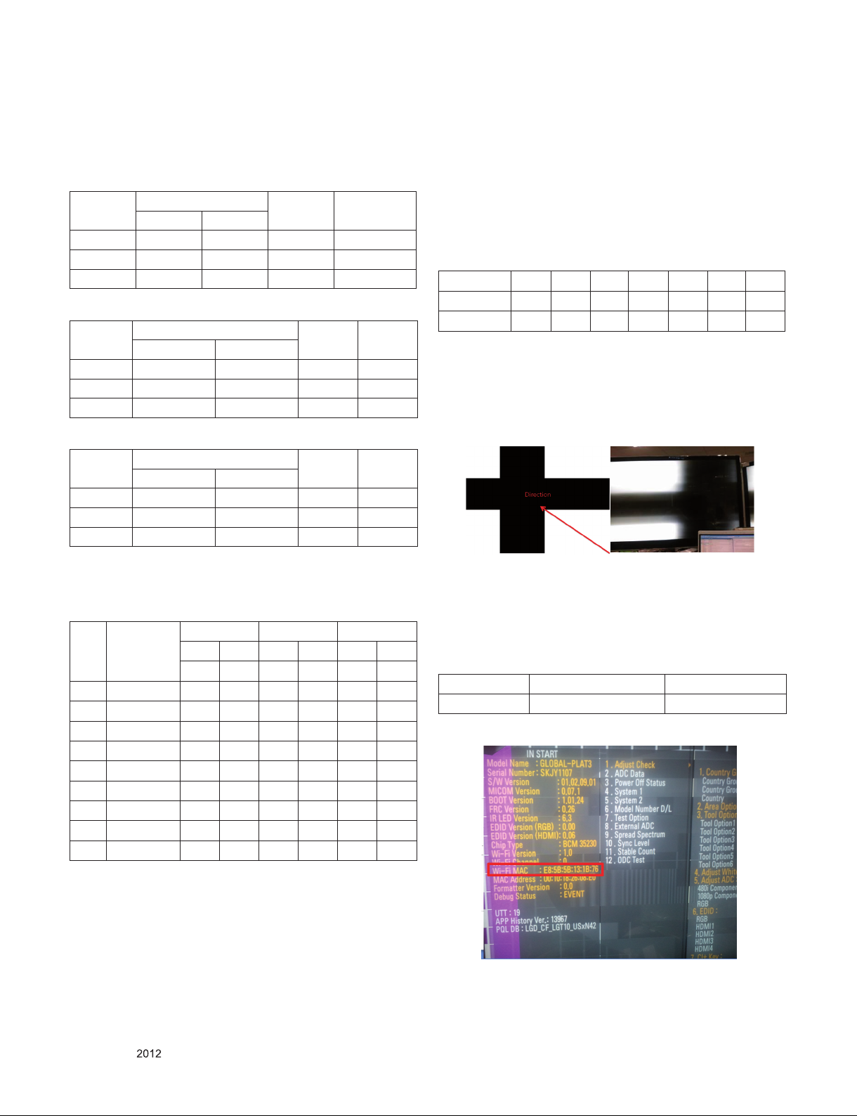
4.5. Option selection per country
4.5.1. Overview
(1) Press ADJ key on the Adj. R/C, and then select Country
Group Menu.
(2) Depending on destination, select KR or US, then on the
lower Country option, select US, CA, MX. Selection is done
using +, - KEY
4.6. Tool Option Inspection
▪ Method: Press Adj. key on the Adj. R/C, then select Tool option.
Model Tool 1 Tool 2 Tool 3 Tool 4 Tool 5 Tool 6 Tool 7
47LM9600-UC
55LM9600-UC
32999 45122 30605 20527 55823 1324 63115
33001 45122 30605 20527 55823 1324 63115
4.7. Local Dimming Inspection (Optional)
4.7.1. ALEF models with local dimming
(1) Press ‘TILT” key of the Adj. R/C and check movin g
patterns. The black bar patterns moves from top to bottom.
If a local dimming function does not work, a whole screen
shows full white
4.4.6.1 ALELF&EDGE LED&IOL White balance table
▪ Edge LED module change color coordinate because of aging time
▪
apply under the color coordinate table, for compensated aging time
Edge (LM860X)
Aging time
GP4
1 0-2 283 293 299 313 320 339
2 3-5 282 291 298 311 319 337
3 6-9 281 290 297 310 318 336
4 10-19 279 289 295 309 316 335
5 20-35 277 284 293 304 314 330
6 36-49 274 279 290 299 311 325
7 50-79 271 277 287 297 308 323
8 80-149 270 274 286 294 307 320
9 Over 150 269 273 285 293 306 319
(Min)
Cool Medium Warm
X Y X Y X Y
269 273 285 293 313 329
4.4.7 THX Adjustment (For US Models)
For THX models, White Balance 4 point automatic control can
be done through the below steps. (Warm axis)
(1) 100 IRE White Balance Adjustment done.
(2) Control Backlight so the Maximum brightness
*In case of 100 IRE adjustment, backlight target value is
125cd/m2.
(3) 4 Point gamma and W/B adjustment done.
* With the controlled maximum brightness, adjust the Gamma
2.2 (60, 40, and 20 IRE / do not adjust at 80 IRE)
*For 10 IRE, set R, G, B gain to 0, 0, and 0, respectively.
4.8. Ship-out mode check (In-stop)
▪ After final inspection, press In-Stop key of the Adj. R/C and
check that the unit goes to Stand-by mode.
▪ After final inspection, Always turn on the Mechanical S/W.
4.9. WIFI MAC ADDRESS CHECK
a. Using RS232
Command Set ACK
Transmission [A][l][][Set ID][][20][Cr] [O][K][x] or [N][G]
b. check the menu on in-start
Note that there are Wi-Fi MAC and MAC address.
Wi-Fi MAC is used for wireless network and MAC address is used
for wired network
Only for training and service purposes
- 15 -
LGE Internal Use OnlyCopyright © LG Electronics. Inc. All rights reserved.
Page 16
5. GND and Internal Pressure check
5.1. Method
(1) GND & Internal Pressure auto-check preparation
- Check that Power Cord is fully inserted to the SET.
(If loose, re-insert)
(2) Perform GND & Internal Pressure auto-check
- Unit fully inserted Power cord; Antenna cable and A/V
arrive to the auto-check process.
- Connect D-terminal to AV JACK TESTER
- Auto CONTROLLER (GWS103-4) ON
- Perform GND TEST
- If NG, Buzzer will sound to inform the operator.
- If OK, changeover to I/P check automatically.
(Remove CORD, A/V form AV JACK BOX)
- Perform I/P test
- If NG, Buzzer will sound to inform the operator.
- If OK, Good lamp will lit up and the stopper will allow the
pallet to move on to next process.
7. Magic Motion Remote Control Inspection
- Requ ired Ins trument s: Ins pection RF-re mote con trol,
Inspection IR-KEY-CODE remote control.
- Prior to the test, AA battery for the RF-remote control should
be adequate.
(Change the battery for each LOT is recommended)
- Test procedures
(1) Press the ‘START’ key on the controller to pair with the set.
(2) Press the ‘OK’ key in the controller and check whether the
cursor appears on the set.
(3) Press ‘Vol+ (STOP)’ key to de-pair with the set.
8. 3D function test
8.1 Test equipment
(1) Pattern Generator MSHG-600 or MSPG-6100 (HDMI 1.4
support)
(2) Pattern: HDMI mode (model No. 872, pattern No. 83)
5.2. Checkpoint
(1) Test voltage
- GND: 1.5KV/min at 100mA
- SIGNAL: 3KV/min at 100mA
(2) TEST time: 1 second
(3) TEST POINT
- GND Test = POWER CORD GND and SIGNAL CABLE
GND.
- Hi-pot Test = POWER CORD GND and LIVE & NEUTRAL.
(4) LEAKAGE CURRENT: At 0.5mArms
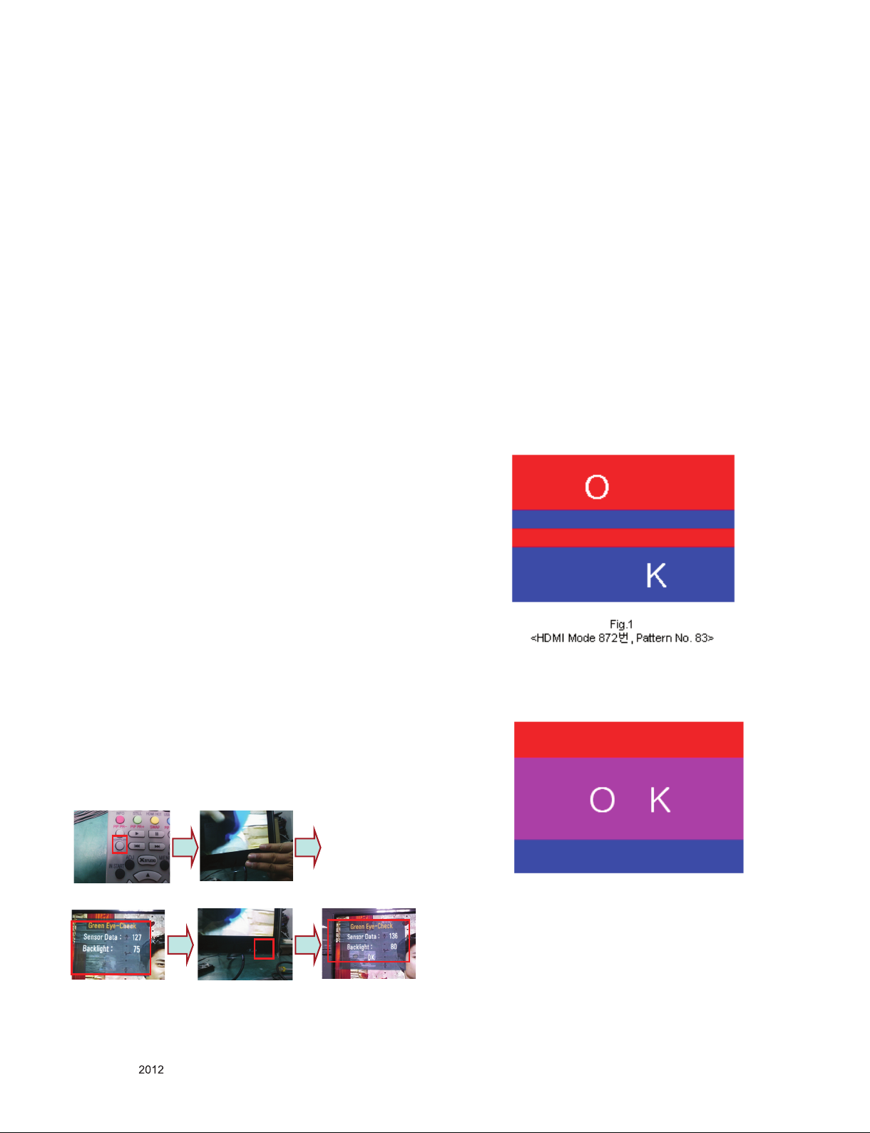
6. EYE-Q Operation check
Step 1) Turn on the TV..
Step 2) Press ' EY E button' o n t he adjustm en t remote -
controller.
Step 3) Cover 'Eye Q sensor' on the front of set with your
hands, hold it for 6 seconds.
Step 4) Check "the Sensor Data" on the screen, make certain
that Data is below 10. If Data isn’t below 10 in 6
seconds, Eye Q sensor would be bad. You should
change Eye Q sensor.
Step 5) Uncover your hands from Eye Q sensor, hold it for 6
seconds.
Step 6) Check "Back Light(xxx)" on the screen, check data
increase . You should change Eye Q sensor.
8.2 Test method
(1) Input 3D test signal as Fig.1.
(2) Press ‘OK” key as a 3D input OSD is shown.
(3) Check pattern as Fig2 without 3D glasses. (3D mode
without 3D glasses)
<Step 2>
<Step 4>
Only for training and service purposes
<Step 3>
<Step 5>
<Step 6>
- 16 -
Fig.2
<OK in 3D mode without 3D glasses>
LGE Internal Use OnlyCopyright © LG Electronics. Inc. All rights reserved.
Page 17
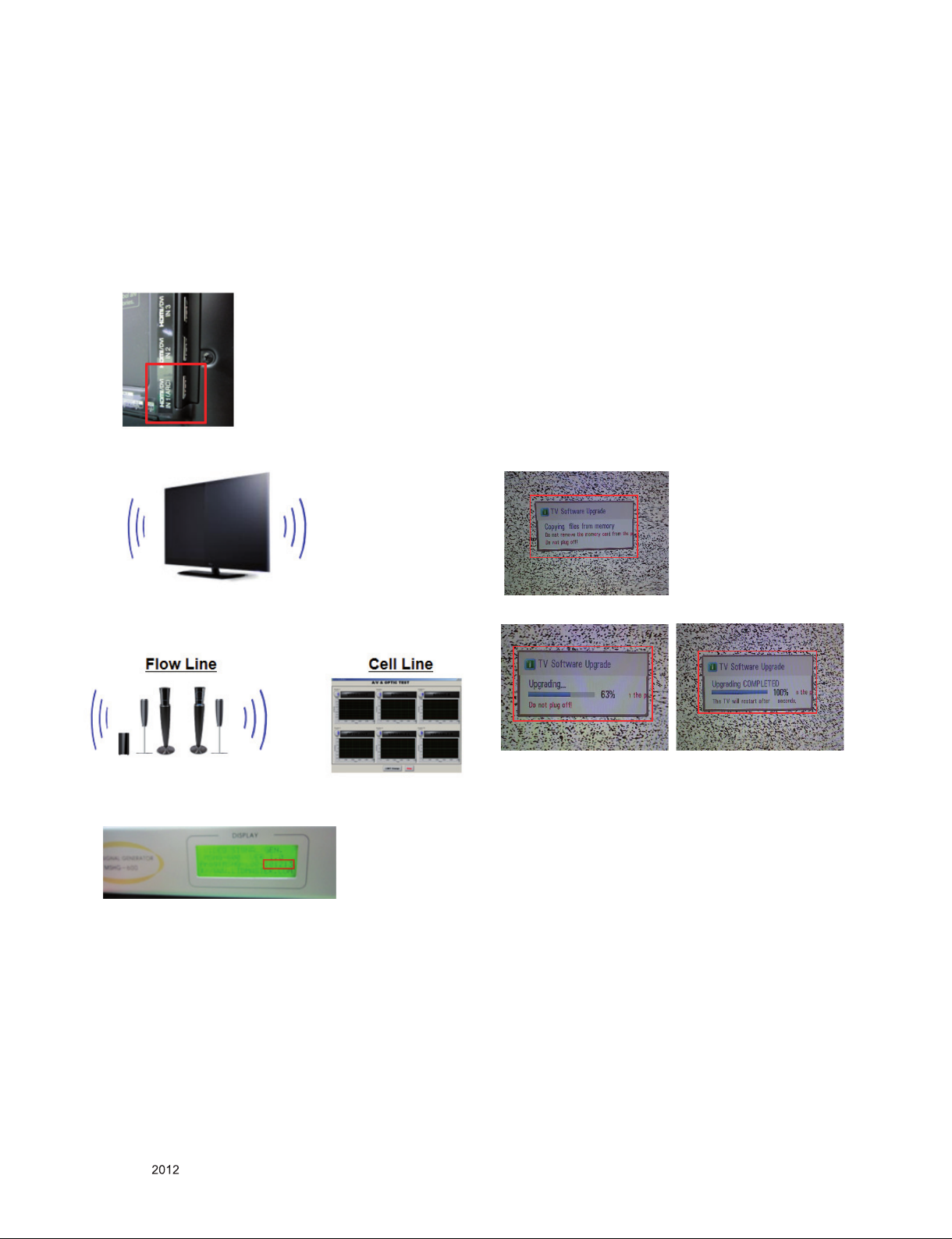
9. HDMI ARC Function Inspection
9.1. Test equipment
- Optic Receiver Speaker
- MSHG-600 (SW: 1220 ↑)
- HDMI Cable (for 1.4 version)
9.2 Test method
(1) Insert the HDMI Cable to the HDMI ARC port from the
master equipment (HDMI1)
(2) Check the sound from the TV Set
10. USB S/W Download
(optional, Service only)
(1) Put the USB Stick to the USB socket
(2) Automatically detecting update file in USB Stick
- If your downloaded program version in USB Stick is lower
than that of TV set, it didn’t work. Otherwise USB data is
automatically detected.
(3) Show the message “Copying files from memory”
(5) Updating Completed, The TV will restart automatically
(6) If your TV is turned on, check your updated version and
Tool option.
* If downloading version is more high than your TV have, TV
can lost all channel data. In this case, you have to channel
recover. If all channel data is cleared, you didn’t have a DTV/
ATV test on production line.
* After downloading, TOOL OPTION setting is needed again.
(1) Push "IN-START" key in service remote controller.
(2) Select "Tool Option 1" and Push “OK” button.
(3) Punch in the number. (Each model has their number.)
(3) Check the Sound from the Speaker or using AV & Optic
TEST program (It’s connected to MSHG-600)
* Remark: Inspect in Power Only Mode and check SW version
in a master equipment
.
(4) Updating is staring.
(5) Updating Completed, The TV will restart automatically
(6) If your TV is turned on, check your updated version and
Tool option.
* If downloading version is more high than your TV have, TV
can lost all channel data. In this case, you have to channel
recover. If all channel data is cleared, you didn’t have a DTV/
ATV test on production line.
* After downloading, TOOL OPTION setting is needed again.
(1) Push "IN-START" key in service remote controller.
(2) Select "Tool Option 1" and Push “OK” button.
(3) Punch in the number. (Each model has their number.)
Only for training and service purposes
- 17 -
LGE Internal Use OnlyCopyright © LG Electronics. Inc. All rights reserved.
Page 18
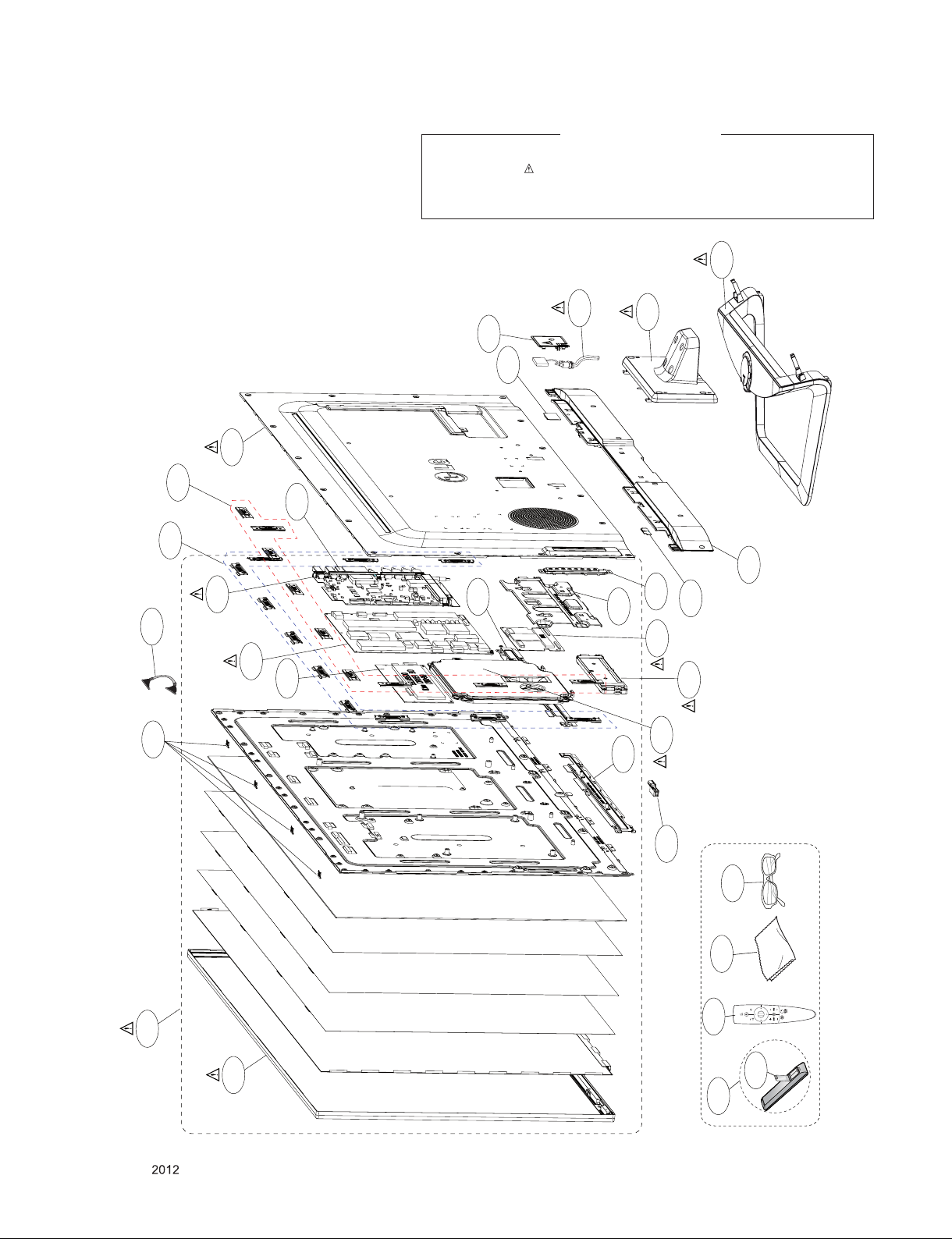
EXPLODED VIEW
IMPORTANT SAFETY NOTICE
Many electrical and mechanical parts in this chassis have special safety-related characteristics. These
parts are identified by in the Schematic Diagram and EXPLODED VIEW.
It is essenti al that these special safet y parts shoul d be replac ed with the same compo nents as
recommended in this manual to prevent X-RADIATION, Shock, Fire, or other Hazards.
Do not modify the original design without permission of manufacturer.
920
LV1
860
830
820
540
400
530
521
200D
710
850
570
700
810
840
910
510
541
122
560
120
121
Except for Location No. 120, 121, 510, 521, 530, 540
200
300
Only for training and service purposes
- 18 -
501
A5
A24
A2
AG1
HOME
LGE Internal Use OnlyCopyright © LG Electronics. Inc. All rights reserved.
/
A21
Page 19
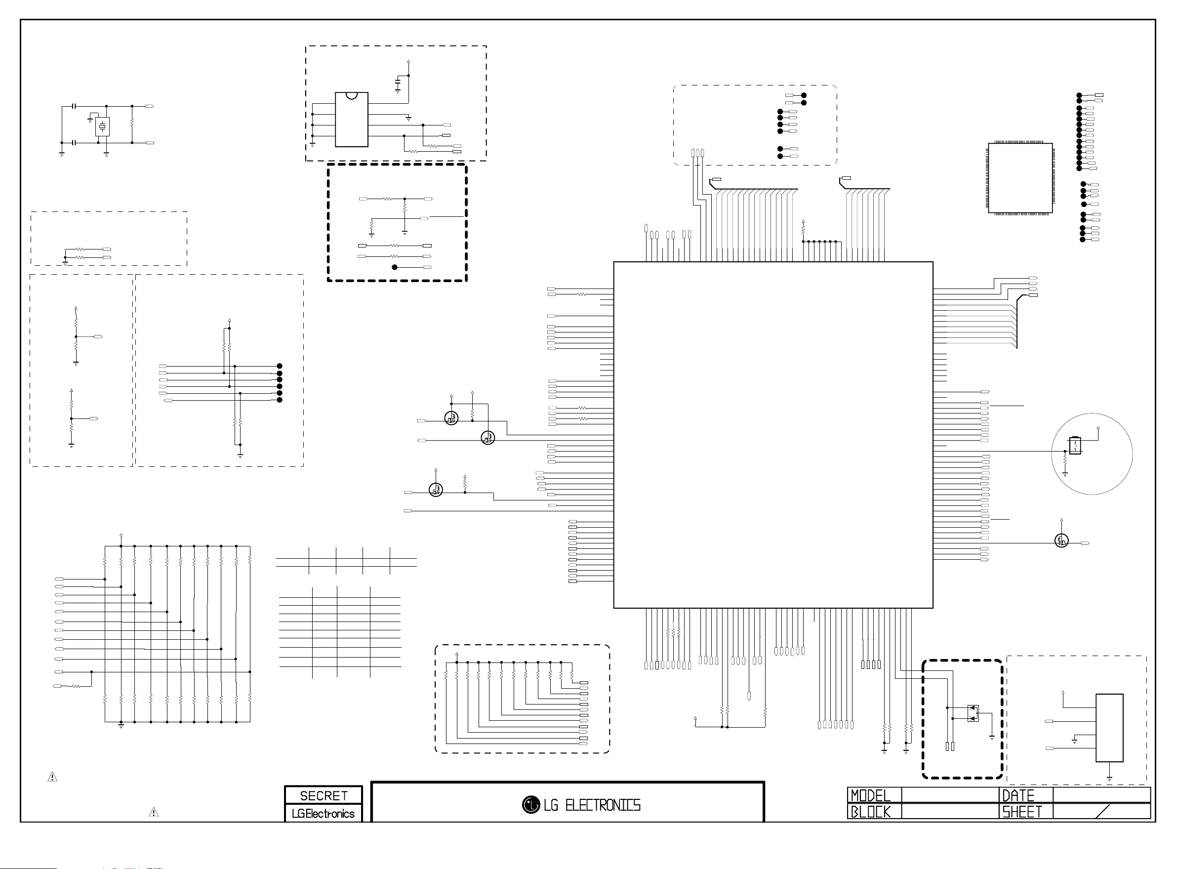
System Configuration
Copyright ⓒ 2012 LG Electronics. Inc. All right reserved.
Only for training and service purposes
LGE Internal Use Only
NVRAM
Clock for LG1152
MAIN Clock(24Mhz)
C100
8pF
50V
X-TAL_1
GND_1
1
2
X101
24MHz
4
3
C101
8pF
50V
GND_2
X-TAL_2
PLL SET[1:0] ==> Internal Pull-UP. N.C is high
00 : CPU clock(1056Mhz), Main0,1/2 DDR (792/792 Mhz)
01 : CPU clock(792Mhz), Main0,1/2 DDR (672/792 Mhz)
10 : CPU clock(1152Mhz), Main0,1/2 DDR (792/672 Mhz)
11 : CPU clock(984Mhz), Main0,1/2 DDR (792/792 Mhz)
BOOT MODE
"11" or "01" : NOR
"10" : eMMC
"00" : NAND
OPT
R102 22
R103 22
OPT
PLLSET1
PLLSET0
R112
XIN_MAIN
1M
XO_MAIN
JTAG I/F FOR MAIN
+3.3V_NORMAL
+3.3V_NORMAL
4.7K
R187
BOOT_MODE1
4.7K
R185
OPT
BOOT_MODE1
+3.3V_NORMAL
4.7K
R188
OPT
4.7K
R186
BOOT_MODE0
TRST_N0
TDI0
TDO0
TMS0
TCK0
SOC_RESET
OPT
OPT
R131 10K
R132 10K
OPT
OPT
R133 10K
R134 10K
BOOT_MODE0
+3.3V_NORMAL
HW_OPT_0
HW_OPT_1
HW_OPT_2
HW_OPT_3
HW_OPT_4
HW_OPT_5
HW_OPT_6
HW_OPT_7
HW_OPT_8
HW_OPT_9
HW_OPT_10
HP_AMP_MUTE
BackEnd 1
BackEnd 2
Pannel Resol
OPTIC I/F
3D Depth IC
DDR Size
CP BOX
FrontEnd 1
FrontEnd 2
OPT
22
R117
10K
URSA5
R110
FRC_EXTERNAL
R100 10K
10K
FRC3
FRC_INTERNAL
R107 10K
R111
FHD
OPTIC
R124 10K
UD
NON_OPTIC
R125 10K
R138 10K
R139 10K
OPT
3D_DEPTH
R140 10K
R145 10K
1GByte
R141 10K
R146 10K
NON_3D DEPTH
CP_BOX
R152 10K
R147 10K
DVB_T2_TUNER
NON_CP_BOX
R153 10K
R148 10K
NON_DVB_T2_TUNER
DVB_S_TUNER
R156 10K
R154 10K
DVB_C2_TUNER
R158 10K
R155 10K
NON_DVB_S_TUNER
NON_DVB_C2_TUNER
ZORAN_FRC
R121 10K
NOT_ZORAN_FRC
R126 10K
MODEL_OPT_0
MODEL_OPT_1
MODEL_OPT_2
MODEL_OPT_3
MODEL_OPT_4
MODEL_OPT_5
MODEL_OPT_6
MODEL_OPT_7
MODEL_OPT_8
MODEL_OPT_9
MODEL_OPT_10
Zoran FRC
(For UD)
MODEL OPTION 8 is just for CP Box
It should not be appiled at MP
THE SYMBOL MARK OF THIS SCHEMETIC DIAGRAM INCORPORATES
SPECIAL FEATURES IMPORTANT FOR PROTECTION FROM X-RADIATION.
FILRE AND ELECTRICAL SHOCK HAZARDS, WHEN SERVICING IF IS
ESSENTIAL THAT ONLY MANUFATURES SPECFIED PARTS BE USED FOR
THE CRITICAL COMPONENTS IN THE SYMBOL MARK OF THE SCHEMETIC.
IC102
R1EX24256BSAS0A
A0
1
A1
A2
VSS
8
2
7
A0’h
3
6
4
5
Place to LVDS Wafer
FRC_RESET
I2C_SCL1
SoC
internal
NO_FRC
FRC
0
0 1
1
HIGH
FHD
OPTIC
3D DEPTH
3D_Depth_IC
DDR Reserved
CP BOX
Enable
T2 Tuner
Support
S Tuner
Support
Support
C2 Tuner
Support
C111
0.1uF
VCC
WP
SCL
SDA
R151 22
4.7K
R113
R160 22
R162 22
MHL_DET
HDMI_INT
LG FRC3
10
0
LOW
UD
NON_OPTIC
NON_3D_Depth_IC
DDR_Default
Disable
Not Support
Not Support
Not Support
Not Support
+3.3V_NORMAL
Write Protection
- Low : Normal Operation
- High : Write Protection
R143
OPT
22
10K
FRC3
R170
SOC_RX
SOC_TX
2N7002K
URSA5
1
R142
OPT
22
FRC3_RESET
3D_DEPTH_RESET
I2C_BE_SDA1I2C_SDA1
I2C_BE_SCL1
LOCAL_DIM_EN
+5V_NORMAL
G
D
Q100
2N7002K
+5V_NORMAL
G
S
D
Q105
OPT
+3.3V_NORMAL
R178
2.2K
I2C_SCL5
I2C_SDA5
I2C_SCL3
I2C_SDA3
+3.3V_NORMAL
S
+3.3V_NORMAL
R203
100K
R180
3.3K
R179
2.2K
OPT
R181
100K
2N7002K
3.3K
R202
G
S
D
Q103
I2C PULL UP
R182
2.2K
R195
2.2K
SOC_RESET
BOOT_MODE1
BOOT_MODE0
ERROR_OUT
/USB_OCD2
/USB_OCD3
M_REMOTE_RX
M_REMOTE_TX
IRB_SPI_MISO
IRB_SPI_MOSI
IRB_SPI_CK
IRB_SPI_SS
AV1_CVBS_DET
DTV_ATV_SELECT
R196
3.3K
R197
3.3K
XIN_MAIN
XO_MAIN
TRST_N0
TMS0
TCK0
TDI0
TDO0
PLLSET1
PLLSET0
EPHY_INT
UART1_RX
UART1_TX
R198
3.3K
I2C_SCL1
I2C_SDA1
I2C_SCL2
I2C_SDA2
I2C_SCL3
I2C_SDA3
I2C_SCL4
I2C_SDA4
I2C_SCL5
I2C_SDA5
I2C_SCL6
I2C_SDA6
R199
3.3K
R150 22
R101 22
R184
R183
1.2K
R104 560
1%
BOOT_MODE1
BOOT_MODE0
1.2K
I2C_SDA1
I2C_SCL1
I2C_SDA2
I2C_SCL2
I2C_SDA3
I2C_SCL3
I2C_SDA4
I2C_SCL4
I2C_SDA5
I2C_SCL5
I2C_SDA6
I2C_SCL6
A22
XIN_MAIN
B22
XO_MAIN
AB16
OPM1
AB17
OPM0
AE3
PORES_N
V23
TRST_N0
U25
TMS0
V25
TCK0
V24
TDI0
U24
TDO0
Y22
TRST_N1
AA22
TMS1
AB20
TCK1
AB21
TDI1
W22
TDO1
AB9
PLLSET1
AB8
PLLSET0
AB15
BOOT_MODE1
AB14
BOOT_MODE0
Y23
EXT_INTR3/GPIO48
W25
EXT_INTR2/GPIO63
W24
EXT_INTR1/GPIO62
W23
EXT_INTR0/GPIO61
Y5
UART0_RX/GPIO49
W6
UART0_TX/GPIO50
AA6
UART1_RX
Y6
UART1_TX
AB5
UART2_RX
AA5
UART2_TX
AB23
SPI_DI0/GPIO39
AB24
SPI_DO0/GPIO38
AA25
SPI_SCLK0/GPIO37
AB25
SPI_CS0/GPIO36
Y25
SPI_DI1/GPIO35
AA23
SPI_DO1/GPIO34
Y24
SPI_SCLK1/GPIO33
AA24
SPI_CS1/GPIO32
AB6
SCL0/GPIO60
AB4
SDA0/GPIO59
AC5
SCL1/GPIO58
AC4
SDA1/GPIO57
AD4
SCL2/GPIO56
AE4
SDA2/GPIO71
AE5
SCL3/GPIO70
AD5
SDA3/GPIO69
AE6
SCL4/GPIO68
AD6
SDA4/GPIO67
AC6
SCL5/GPIO66
AC7
SDA5/GPIO65
FPGA_LVDS_INFO
USB_CTL3
DiiVA_POD_CTL
M25
M24
M23
N23
T27
EB_CS3/GPIO64
EB_CS2/GPIO79
EB_CS1/GPIO78
EB_CS0/GPIO77
RMII_REF_CLK
RMII_CRS_DV
RMII_MDIO
RMII_MDC
AD2
AB1
AB2
AB3
AC2
R105 22
EPHY_MDC
EPHY_MDIO
EPHY_REFCLK
EPHY_CRS_DV
for DiiVA(China)
SEL_USB3
SEL_USB2
SEL_USB1
EB_ADDR[0-14]
EB_OE_N
EB_BE_N1
EB_BE_N0
EB_WE_N
T28
U27
EB_OE_N
EB_WE_N
U26
U28
EB_WAIT
EB_BE_N1
J22
K22
J23
EB_BE_N0
EB_ADDR17/GPIO84
EB_ADDR16/GPIO83
EB_ADDR15/GPIO82
EB_ADDR[11]
EB_ADDR[12]
EB_ADDR[13]
EB_ADDR[14]
L26
L27
L25
N26
EB_ADDR14
EB_ADDR13
EB_ADDR12
EB_ADDR[9]
EB_ADDR[8]
EB_ADDR[10]
N27
M26
L28
EB_ADDR9
EB_ADDR11
EB_ADDR10
IC100
LG1152D-B1
LG1152_NON_RM
RMII_TXEN
RMII_TXD1
RMII_TXD0
RMII_RXD1
RMII_RXD0
CAM_CE1_N
CAM_CE2_N
CAM_CD1_N
CAM_CD2_N
CAM_VS1_N
CAM_VS2_N
CAM_IREQ_N
CAM_RESET
CAM_INPACK_N
AC3
AE1
AD3
AD1
W26
V28
Y27
Y26
W28
W27
AA28
AB26
AA27
AA26
R108 22
R106 22
EPHY_EN
EPHY_TXD1
EPHY_RXD0
EPHY_TXD0
EPHY_RXD1
+3.3V_NORMAL
/PCM_CE2
/PCM_CE1
CAM_CD2_N
CAM_CD1_N
CI
10K
R166
CAM_IREQ_N
CI
R167 10K
PCM_RST
CAM_INPACK_N
EPHY_INT
EB_ADDR[5]
EB_ADDR[7]
EB_ADDR[6]
L24
L23
K28
EB_ADDR8
EB_ADDR7
EB_ADDR6
EB_ADDR5
CAM_VCCEN_N
CAM_WAIT_N
CAM_REG_N
CAM_IOIS16_N
Y28
V27
V26
CAM_REG_N
CAM_WAIT_N
CI
10K
R168
PCM_5V_CTL
HP_DET
EB_ADDR[3]
EB_ADDR[2]
EB_ADDR[4]
K27
K26
K25
K24
EB_ADDR4
EB_ADDR3
EB_ADDR2
SC_CLK/GPIO90
SC_DETECT/GPIO93
R25
U23
T25
SMARTCARD_DET
SMARTCARD_CLK
SEL_USB1
SEL_USB2
SEL_USB3
/RST_PHY
SC_DET
DiiVA_POD_CTL
+3.3V_NORMAL
EB_ADDR[1]
EB_ADDR[0]
10K
R109
K23
V22
U22
EB_ADDR1
EB_ADDR0
EB_DATA15
EB_DATA14
SC_VCCEN/GPIO89
SC_VCC_SEL/GPIO88
SC_RST/GPIO91
SC_DATA/GPIO92
T24
T23
R24
SMARTCARD_RST
SMARTCARD_VCC
SMARTCARD_DATA
SMARTCARD_PWR_SEL
T22
R22
P22
N22
M22
EB_DATA9
EB_DATA13
EB_DATA12
EB_DATA11
EB_DATA10
SD_CLK/GPIO76
SD_CMD/GPIO73
SD_CD_N/GPIO75
SD_WP_N/GPIO74
SD_DATA3/GPIO72
C22
C23
A23
B23
A24
MOTOR_CCW
MOTOR_CLOSE_SW
MO_SENS_TO_MAIN_UP
MO_SENS_TO_MAIN_DOWN
EB_DATA[0-7]
EB_DATA[0]
EB_DATA[1]
EB_DATA[3]
EB_DATA[2]
EB_DATA[4]
EB_DATA[5]
EB_DATA[6]
EB_DATA[7]
L22
T26
R28
R27
R26
P28
P27
P26
N28
EB_DATA8
EB_DATA7
EB_DATA6
EB_DATA5
EB_DATA4
EB_DATA3
EB_DATA2
EB_DATA1
EB_DATA0
EMMC_RST
EMMC_CLK
EMMC_CMD
EMMC_DATA7
EMMC_DATA6
EMMC_DATA5
EMMC_DATA4
EMMC_DATA3
EMMC_DATA2
EMMC_DATA1
EMMC_DATA0
NAND_CS1
NAND_CS0
NAND_ALE
NAND_CLE
NAND_REN
NAND_WEN
SD_DATA2/GPIO87
SD_DATA1/GPIO86
SD_DATA0/GPIO85
USB_DP1
USB_DM1
USB_DP2
USB_DM2
USB_TXR_RKL
USB_ANALOGTEST
BT_USB_DP
BT_USB_DM
BT_TXR_RKL
BT_ANALOGTEST
R173
Y4
C25
B25
AA1
AA2
AA4
22
22
OPT
R175
R176
R174
B24
C24
A25
MOTOR_CW
IR_B_RESET
MOTOR_OPEN_SW
B27
A27
A26
B26
USB_DM3
USB_DP3
USB_HUB_IC_IN_DM
USB_HUB_IC_IN_DP
Place near Jack side
E28
F27
F26
C26
EMMC_DATA[7]
E27
EMMC_DATA[6]
E26
EMMC_DATA[5]
D27
EMMC_DATA[4]
D28
EMMC_DATA[3]
C27
EMMC_DATA[2]
C28
EMMC_DATA[1]
D26
EMMC_DATA[0]
R23
P24
N25
P23
N24
P25
AC1
GPIO31
V7
GPIO30
W5
GPIO29
W4
GPIO28
V6
GPIO27
V5
GPIO26
V4
GPIO25
U6
GPIO24
U5
GPIO23
U4
GPIO22
T6
GPIO21
T5
GPIO20
T4
GPIO19
R6
GPIO18
R5
GPIO17
R4
GPIO16
P6
GPIO15
P5
GPIO14
P4
GPIO13
N6
GPIO12
N5
GPIO11
N4
GPIO10
N3
GPIO9
M6
GPIO8
AC23
GPIO7
AC24
GPIO6
AE24
GPIO5
AD23
GPIO4
AE23
GPIO3
AC22
GPIO2
AD22
GPIO1
AE22
GPIO0
OPT
WIFI_DP
LG1152 B1
MAIN & GPIO
RCLAMP0502BA
WIFI_DM
M25
M24
M23
N23
T27
T28
U27
U26
U28
J22
K22
J23
EB_OE_N
EB_WE_N
EB_WAIT
EB_BE_N1
EB_BE_N0
A22
XIN_MAIN
B22
EB_CS3/GPIO64
EB_CS2/GPIO79
EB_CS1/GPIO78
EB_CS0/GPIO77
XO_MAIN
AB16
OPM1
EB_ADDR17/GPIO84
EB_ADDR16/GPIO83
AB17
OPM0
AE3
PORES_N
V23
TRST_N0
U25
TMS0
V25
TCK0
V24
TDI0
U24
TDO0
Y22
TRST_N1
AA22
TMS1
AB20
TCK1
AB21
TDI1
W22
TDO1
AB9
PLLSET1
AB8
PLLSET0
AB15
BOOT_MODE1
AB14
BOOT_MODE0
Y23
EXT_INTR3/GPIO48
W25
EXT_INTR2/GPIO63
W24
EXT_INTR1/GPIO62
W23
EXT_INTR0/GPIO61
Y5
UART0_RX/GPIO49
W6
UART0_TX/GPIO50
AA6
UART1_RX
Y6
UART1_TX
AB5
UART2_RX
AA5
UART2_TX
AB23
SPI_DI0/GPIO39
AB24
SPI_DO0/GPIO38
AA25
SPI_SCLK0/GPIO37
AB25
SPI_CS0/GPIO36
Y25
SPI_DI1/GPIO35
AA23
SPI_DO1/GPIO34
Y24
SPI_SCLK1/GPIO33
AA24
SPI_CS1/GPIO32
AB6
SCL0/GPIO60
AB4
SDA0/GPIO59
AC5
SCL1/GPIO58
AC4
SDA1/GPIO57
AD4
SCL2/GPIO56
AE4
SDA2/GPIO71
AE5
SCL3/GPIO70
AD5
SDA3/GPIO69
AE6
SCL4/GPIO68
AD6
SDA4/GPIO67
AC6
SCL5/GPIO66
AC7
SDA5/GPIO65
RMII_REF_CLK
RMII_CRS_DV
RMII_MDIO
RMII_MDC
RMII_TXEN
RMII_TXD1
RMII_TXD0
RMII_RXD1
RMII_RXD0
CAM_CE1_N
CAM_CE2_N
AD2
AB1
AB2
AB3
AC2
AC3
AE1
AD3
AD1
W26
V28
Y27
LG1152_RM
IC100-*1
OPTIC_FPGA_RESET
OPTIC_SERDES_RESET
3D_DEPTH_RESET
/RST_PHY
OLED_TCON_RESET
HW_OPT_9
HW_OPT_7
HW_OPT_8
DSUB_DET
SC_DET
COMP1_DET
HW_OPT_5
HW_OPT_6
M_RFModule_ISP
HW_OPT_10
M_RFModule_RESET
FRC_RESET
HW_OPT_2
HW_OPT_1
HW_OPT_0
HW_OPT_4
FLASH_WP
/RST_HUB
HW_OPT_3
HP_DET
RF_SWITCH_CTL
/TU_RESET
/S2_RESET
OPT
D100
I2C_SDA2
I2C_SCL2
SMARTCARD_DATA
SMARTCARD_RST
SMARTCARD_PWR_SEL
SMARTCARD_VCC
SMARTCARD_DET
L26
L27
L25
N26
N27
M26
L28
L24
L23
K28
K27
K26
K25
K24
K23
V22
U22
T22
R22
P22
N22
M22
L22
T26
R28
R27
R26
P28
P27
P26
N28
EB_ADDR9
EB_ADDR8
EB_ADDR7
EB_ADDR6
EB_ADDR5
EB_ADDR4
EB_ADDR3
EB_ADDR2
EB_ADDR1
EB_ADDR0
EB_DATA9
EB_DATA8
EB_DATA7
EB_DATA6
EB_DATA5
EB_DATA4
EB_DATA3
EB_DATA2
EB_DATA1
EB_ADDR14
EB_ADDR13
EB_ADDR12
EB_ADDR11
EB_ADDR15/GPIO82
CAM_CD1_N
CAM_CD2_N
CAM_VS1_N
CAM_VS2_N
CAM_IREQ_N
Y26
W28
W27
AA28
AB26
EB_DATA0
EB_ADDR10
EB_DATA15
EB_DATA14
EB_DATA13
EB_DATA12
EB_DATA11
EB_DATA10
E28
EMMC_RST
F27
EMMC_CLK
F26
EMMC_CMD
C26
EMMC_DATA7
E27
EMMC_DATA6
E26
EMMC_DATA5
D27
EMMC_DATA4
D28
EMMC_DATA3
C27
EMMC_DATA2
C28
EMMC_DATA1
D26
EMMC_DATA0
R23
NAND_CS1
P24
NAND_CS0
N25
NAND_ALE
P23
NAND_CLE
N24
NAND_REN
P25
NAND_WEN
AC1
GPIO31
V7
GPIO30
W5
GPIO29
W4
GPIO28
V6
GPIO27
V5
GPIO26
V4
GPIO25
U6
GPIO24
U5
GPIO23
U4
GPIO22
T6
GPIO21
T5
GPIO20
T4
GPIO19
R6
GPIO18
R5
GPIO17
R4
GPIO16
P6
GPIO15
P5
GPIO14
P4
GPIO13
N6
GPIO12
N5
GPIO11
N4
GPIO10
N3
GPIO9
M6
GPIO8
AC23
GPIO7
AC24
GPIO6
AE24
GPIO5
AD23
GPIO4
AE23
GPIO3
AC22
GPIO2
AD22
GPIO1
AE22
CAM_RESET
CAM_INPACK_N
CAM_VCCEN_N
CAM_WAIT_N
CAM_REG_N
CAM_IOIS16_N
Y28
V27
V26
AA27
AA26
GPIO0
SC_CLK/GPIO90
SC_DETECT/GPIO93
SC_VCCEN/GPIO89
SC_VCC_SEL/GPIO88
SC_RST/GPIO91
SC_DATA/GPIO92
SD_CLK/GPIO76
SD_CMD/GPIO73
SD_CD_N/GPIO75
SD_WP_N/GPIO74
SD_DATA3/GPIO72
SD_DATA2/GPIO87
SD_DATA1/GPIO86
SD_DATA0/GPIO85
USB_DP1
USB_DM1
USB_DP2
USB_DM2
USB_TXR_RKL
USB_ANALOGTEST
BT_USB_DP
BT_USB_DM
BT_TXR_RKL
BT_ANALOGTEST
Y4
R25
U23
T25
T24
T23
R24
C22
C23
A23
B23
A24
B24
C24
A25
B27
A27
A26
B26
C25
B25
AA1
AA2
AA4
SMARTCARD_CLK
MOTOR_CLOSE_SW
MOTOR_OPEN_SW
MOTOR_CW
MOTOR_CCW
MO_SENS_TO_MAIN_UP
MO_SENS_TO_MAIN_DOWN
OPTIC_FPGA_RESET
OPTIC_SERDES_RESET
OLED_TCON_RESET
FPGA_LVDS_INFO
IRB_SPI_MISO
IRB_SPI_MOSI
IRB_SPI_CK
IRB_SPI_SS
IR_B_RESET
EMMC_RST
EMMC_CLK
EMMC_CMD
EMMC_DATA[0-7]
+3.3V_NORMAL
SW1
JTP-1127WEM
12
2.7K
R201
DEBUG
For ISP
Delete PV
4 3
1/16W
5%
+5V_NORMAL
G
D
HDMI_S/W_RESET
S
Q104
2N7002K
Debug
+3.3V_NORMAL
UART1_RX
UART1_TX
1
P100
12507WS-04L
1
DEBUG
2
3
4
5
Page 20
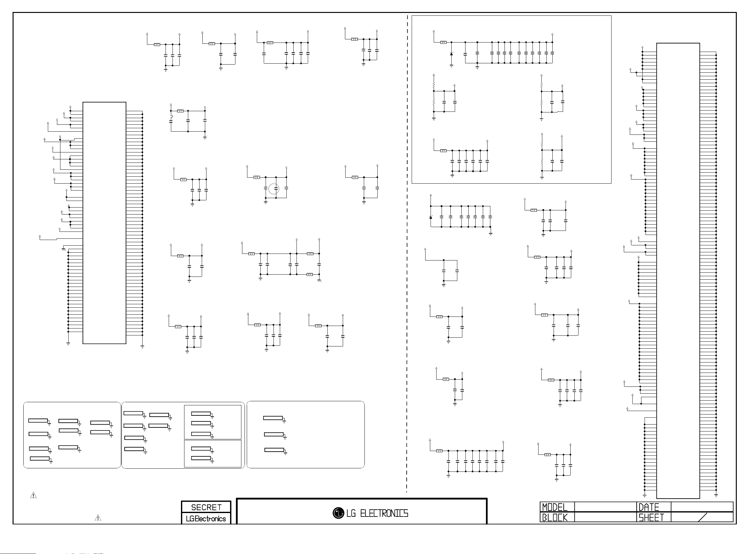
+1.0V_VDD
Copyright ⓒ 2012 LG Electronics. Inc. All right reserved.
Only for training and service purposes
LGE Internal Use Only
Max 360mA
AVDD10_DEMOD
L304
BLM18PG121SN1D
10uFC312
C318 0.1uF
C321 0.1uF
+1.0V_VDD
L302
BLM18PG121SN1D
LG1152A
IC101
VDD33
VDD33_CVBS
VDD33_HDMI
VDD33_XTAL
VDD25_VSB
VDD25_CVBS
VDD25_REF
VDD25_COMP
VDD25_AUD
VDD25_LVTX
VDD18_A
AVDD10_DEMOD
AVDD10_VSB
AVDD10_LVTX
VDDC_XTAL
+2.5V_NORMAL
For HDCP OTP
Will be change to LOW for MP
For HeatSinK, AL Block / SMD Top
MDS62110218
MDS62110218
MDS62110218
M300
M303
M306
M307
MDS62110218
AVSS25_REF
M301
MDS62110218
M302
MDS62110218
M321
MDS62110218
P1
P2
P14
R14
F18
H16
M16
L15
R13
R12
V13
P10
R10
P9
R9
V7
J16
P6
P7
V6
B18
G12
G13
N1
N2
G6
G7
R15
K15
D17
D18
N7
L16
G4
N10
K16
D16
G5
G8
G9
G10
G11
G14
G15
H4
H5
H6
H7
H8
H9
H10
H11
H12
H13
H14
H15
J4
J5
J6
J7
ALBLOCK
ALBLOCK
ALBLOCK
VDD33_1
VDD33_2
AVDD33_CVBS_1
AVDD33_CVBS_2
AVDD33_HDMI_1
AVDD33_HDMI_2
VDD33_XTAL
VDD25_VSB
VDD25_CVBS_2
VDD25_CVBS_1
VDD25_CVBS_3
AVDD25_REF
VDD25_COMP_3
VDD25_COMP_1
VDD25_COMP_2
VDD25_COMP_4
VDD25_AAD
VDD25_AUD_1
VDD25_AUD_2
VDD25_AUD_3
VDD25_LVTX_1
VDD25_LVTX_2
VDD25_LVTX_3
VDD18_1
VDD18_2
VDDC10_1
VDDC10_2
AVDD10_CVBS
AVDD10_VSB
AVDD10_LVTX_1
AVDD10_LVTX_2
AVDD10_LLPLL
VDDC_XTAL
VQPS
AVSS25_REF
GND_XTAL
GND_1
GND_2
GND_3
GND_4
GND_5
GND_6
GND_7
GND_8
GND_9
GND_10
GND_11
GND_12
GND_13
GND_14
GND_15
GND_16
GND_17
GND_18
GND_19
GND_20
GND_21
GND_22
GND_23
GND_24
M304
MDS62110218
M305
MDS62110218
HEATSINK
HEATSINK
GND_25
GND_26
GND_27
GND_28
GND_29
GND_30
GND_31
GND_32
GND_33
GND_34
GND_35
GND_36
GND_37
GND_38
GND_39
GND_40
GND_41
GND_42
GND_43
GND_44
GND_45
GND_46
GND_47
GND_48
GND_49
GND_50
GND_51
GND_52
GND_53
GND_54
GND_55
GND_56
GND_57
GND_58
GND_59
GND_60
GND_61
GND_62
GND_63
GND_64
GND_65
GND_66
GND_67
GND_68
GND_69
GND_70
GND_71
GND_72
GND_73
GND_74
GND_75
GND_76
GND_77
GND_78
GND_79
GND_80
GND_81
GND_82
GND_83
GND_84
GND_85
GND_86
GND_87
GND_88
GND_89
GND_90
J8
J9
J10
J11
J12
J13
J14
J15
K4
K5
K6
K7
K8
K9
K10
K11
K12
K13
K14
L4
L5
L6
L7
L8
L9
L10
L11
L12
L13
L14
M4
M5
M6
M7
M8
M9
M10
M11
M12
M13
M14
M15
M17
N4
N5
N6
N8
N9
N11
N12
N13
N14
N15
N16
P3
P4
P5
P13
P15
P16
R3
R16
R17
R18
T13
U13
SMD Bottom
M315
MDS62110205
M312
MDS62110205
M313
MDS62110205
M314
MDS62110205
ESD
ESD
OPT
ESD
THE SYMBOL MARK OF THIS SCHEMETIC DIAGRAM INCORPORATES
SPECIAL FEATURES IMPORTANT FOR PROTECTION FROM X-RADIATION.
FILRE AND ELECTRICAL SHOCK HAZARDS, WHEN SERVICING IF IS
ESSENTIAL THAT ONLY MANUFATURES SPECFIED PARTS BE USED FOR
THE CRITICAL COMPONENTS IN THE SYMBOL MARK OF THE SCHEMETIC.
11/05/31
LG1152AN-B2
+1.8V_NORMAL
10uFC421
+2.5V_NORMAL
L326
BLM18PG121SN1D
10uFC422
Max 100mA
L324
BLM18PG121SN1D
10uFC414
VDD18_A
VDD25_CVBS
C417 0.1uF
On Package Decap : 0.1uF *1ea
Max 50mA
L322
BLM18PG121SN1D
10uFC401
VDD25_AUD
+2.5V_NORMAL
On Package Decap : 0.1uF *1ea
+3.3V_NORMAL
Max 35mA
L319
BLM18PG121SN1D
10uFC398
VDD33_CVBS
C403 0.1uF
C408 0.1uF
On Package Decap : 0.1uF *1ea
For Tuner Sensitivity / Under DDR
M318
MDS62110205
M317
MDS62110205
OPT
ESD
M308
MDS62110205
M309
MDS62110206
M322
MDS62110205
For Tuner Sensitivity / Under TUNER
M310
MDS62110205
M311
MDS62110205
C423 0.1uF
C419 0.1uF
C409 0.1uF
GASKET_8.0X6.0X7.5H
GASKET except ATSC
SMR-T-6-6.5-8
OPT
GASKET_8.0X6.0X7.5H
OPT
ATSC
10uFC305
Max 1mA
VDDC_XTAL
C313 0.1uF
+2.5V_NORMAL
+1.0V_VDD
10uFC359
L313
BLM18PG121SN1D
On Package Decap : 0.1uF *1ea
+2.5V_NORMAL
L315
BLM18PG121SN1D
10uFC379
On Package Decap : 0.1uF *1ea
+3.3V_NORMAL
L323
BLM18PG121SN1D
On Package Decap : 0.1uF *1ea
SMD TOP FOR ESD
For ATSC
L308
BLM18PG121SN1D
Max 250mA
VDD25_LVTX
10uFC375
C385 0.1uF
C386 0.1uF
Max 256mA
VDD33_HDMI
10uFC413
OPT
C405 0.1uF
M316
MDS62110217
ESD
M320
MDS62110217
M319
MDS62110217
Max 250mA
C416 0.1uF
ESD
ESD
10uFC366
C368 0.1uF
C390 0.1uF
VDD25_COMP
C407 0.1uF
Max 12mA
AVDD10_VSB
10uFC369
C393 0.1uF
C370 0.1uF
Max 10mA
VDD25_REF
L321
BLM15BD121SN1
L320
BLM15BD121SN1
AVSS25_REF
+3.3V_NORMAL
L309
BLM18PG121SN1D
+1.0V_VDD
L305
BLM18PG121SN1D
On Package Decap : 0.1uF *1ea
+2.5V_NORMAL
L325
BLM18PG121SN1D
On Package Decap : 0.1uF *1ea
C400 0.1uF
Max 1mA
VDD33_XTAL
10uFC371
C381 0.1uF
Max 35mA
AVDD10_LVTX
10uFC332
C333 0.1uF
Max 28mA
VDD25_VSB
10uFC415
C338 0.1uF
C418 0.1uF
+1.5V_Bypass Cap
+1.5V_DDR
L300
BLM18PG121SN1D
5V
ZD301
ESD_LG1152
VCC1.5V_MAIN
Max 40mA
VREF_M0
R300
1K 1%
0.1uF
R301
1K 1%
On Package Decap : 0.1uF *1ea
+1.5V_DDR
BLM18PG121SN1D
On Package Decap : 0.1uF *2ea
+0.9V_VDD
10uFC301
5V
ZD300
ESD_LG1152
On Package Decap : 0.1uF *6ea
+0.9V_VDD
On Package Decap : 0.1uF *1ea
+1.8V_NORMAL
L312
BLM18PG121SN1D
On Package Decap:0.1uF *1ea
+1.8V_NORMAL
On Package Decap:0.1uF *1ea
+3.3V_NORMAL
L310
BLM18PG121SN1D
On Package Decap : 0.1uF *1ea
C308
C300
L301
10uFC303
10uFC307
Max 20mA
10uFC347
Max 120mA
VDD18_LVTX
10uFC374
Max 93mA
VDD18_LVRX
L318
BLM18PG121SN1D
10uFC397
10uFC372
1000pF
C306 0.1uF
C314 0.1uF
C353 0.1uF
C382 0.1uF
C404 0.1uF
C377 0.1uF
10uFC326
C316 0.1uF
C310 0.1uF
Max 5900mA
C322 0.1uF
C319 0.1uF
C388 0.1uF
C383 0.1uF
(18)
10uFC302
C317 0.1uF
C311 0.1uF
C323 0.1uF
C320 0.1uF
On Package Decap : 0.1uF *3ea
Max 340mA
VCC1.5V_DE
C336 0.1uF
C340 0.1uF
C327 0.1uF
C325 0.1uF
VDD33
C392 0.1uF
C394 0.1uF
C399 0.1uF
C391 0.1uF
Max 680mA
VCC1.5V_MAIN
C329 0.1uF
C334 0.1uF
C337 0.1uF
VCC1.5V_MAIN
C342 0.1uF
R302
R303
C343 0.1uF
1K 1%
1K 1%
C346 0.1uF
Max 40mA
VREF_M1
0.1uF
C350
C362
On Package Decap : 0.1uF *1ea
Max 40mA
VCC1.5V_DE
R304
R305
VREF_M2
1K 1%
0.1uF
1K 1%
C363
C351
On Package Decap : 0.1uF *1ea
10uFC309
10uFC341
Max 6mA
C315 0.1uF
Max 1320mA
C345 0.1uF
MAIN_XTAL
C324 0.1uF
AVDD10_OSPREY
C348 0.33uF
+0.9V_VDD
+1.0V_VDD
L303
BLM18PG121SN1D
L306
BLM18PG121SN1D
On Package Decap : 0.1uF *3ea
+1.8V_NORMAL
L316
BLM18PG121SN1D
10uFC395
On Package Decap:0.1uF *1ea
+1.8V_NORMAL
+3.3V_NORMAL
BLM18PG121SN1D
L314
BLM18PG121SN1D
L317
10uFC396
VDD18_MAIN_XTAL
10uFC378
Max 48.8mA
VDD33_USB
C402 0.1uF
1000pF
1000pF
C349 0.33uF
Max 49mA
VDD18
C410 0.1uF
Max 31mA
C384 0.1uF
C389 0.1uF
C406 0.1uF
C411 0.1uF
C304 0.1uF
For secure BOOT OTP
Will be change to LOW for MP
LG1152
MAIN POWER
VDD33_USB
VDD18_LVTX
VDD18_LVRX
VDD18_MAIN_XTAL
VCC1.5V_DE
VCC1.5V_MAIN
VREF_M1
VREF_M0
AVDD10_OSPREY
+0.9V_VDD
+0.9V_VDD
MAIN_XTAL
VDD18
LG1152D
VDD33
U8
U9
U10
V8
V9
V10
J21
K21
AA10
AA11
VDD18
W18
W19
Y18
Y19
AG28
AH27
AA7
AA8
AA9
AG1
AA12
AA13
AB12
J28
B28
G22
F9
G8
G9
G10
G11
H8
H9
H10
H11
F22
G13
G14
G16
G17
G18
G19
G20
G21
H13
H14
H16
H17
H18
H19
H20
H21
VREF_M2
L4
F13
G12
F14
G15
L20
M20
M21
M27
M28
N20
N21
P20
P21
R20
R21
K8
K9
K10
K11
L8
L9
L10
L11
M8
M9
M10
M11
N8
N9
N10
N11
P8
P9
P10
P11
R8
R9
R10
R11
Y7
Y8
AF1
F28
H22
AA19
G23
G7
H7
H12
H15
J7
J8
J9
J10
J11
J12
J13
J14
J15
J16
J17
J18
J19
J20
K7
K12
IC100
LG1152D-B1
VDD33_1
VDD33_2
VDD33_3
VDD33_4
VDD33_5
VDD33_6
AVDD33_USB_1
AVDD33_USB_2
AVDD33_BT_USB_1
AVDD33_BT_USB_2
VDD18_1
VDD18_2
VDD18_3
VDD18_4
VDD18_5
VDD18_6
VDD18_LTX_1
VDD18_LTX_2
VDD18_LTX_3
VDD18_LTX_4
VDD18_LVRX_1
VDD18_LVRX_2
VDD18_LVRX_3
VDD18_DISPPLL
VDD18_DR3PLL
VDD18_MAIN_XTAL
VDD15_M2_1
VDD15_M2_2
VDD15_M2_3
VDD15_M2_4
VDD15_M2_5
VDD15_M2_6
VDD15_M2_7
VDD15_M2_8
VDD15_M2_9
VDD15_M0_1
VDD15_M0_2
VDD15_M0_3
VDD15_M0_4
VDD15_M0_5
VDD15_M0_6
VDD15_M0_7
VDD15_M0_8
VDD15_M0_9
VDD15_M0_10
VDD15_M0_11
VDD15_M0_12
VDD15_M0_13
VDD15_M0_14
VDD15_M0_15
VDD15_M0_16
VDD15_M0_17
VREF_M2_0
VREF_M1_0
VREF_M1_1
VREF_M0_0
VREF_M0_1
VDDC10_OSPREY_1
VDDC10_OSPREY_2
VDDC10_OSPREY_3
VDDC10_OSPREY_4
VDDC10_OSPREY_5
VDDC10_OSPREY_6
VDDC10_OSPREY_7
VDDC10_OSPREY_8
VDDC10_OSPREY_9
VDDC10_OSPREY_10
VDDC10_OSPREY_11
VDDC09_1
VDDC09_2
VDDC09_3
VDDC09_4
VDDC09_5
VDDC09_6
VDDC09_7
VDDC09_8
VDDC09_9
VDDC09_10
VDDC09_11
VDDC09_12
VDDC09_13
VDDC09_14
VDDC09_15
VDDC09_16
VDDC09_17
VDDC09_18
VDDC09_19
VDDC09_20
VDDC09_21
VDDC09_22
VDDC09_23
VDDC09_24
VDD09_LTX_1
VDD09_LTX_2
VDD09_LTX_3
AVDD09_DR3PLL
VDDC_MAIN_XTAL
SP_VQPS
GND_MAIN_XTAL
GND_1
GND_2
GND_3
GND_4
GND_5
GND_6
GND_7
GND_8
GND_9
GND_10
GND_11
GND_12
GND_13
GND_14
GND_15
GND_16
GND_17
GND_18
GND_19
GND_20
3
GND_21
GND_22
GND_23
GND_24
GND_25
GND_26
GND_27
GND_28
GND_29
GND_30
GND_31
GND_32
GND_33
GND_34
GND_35
GND_36
GND_37
GND_38
GND_39
GND_40
GND_41
GND_42
GND_43
GND_44
GND_45
GND_46
GND_47
GND_48
GND_49
GND_50
GND_51
GND_52
GND_53
GND_54
GND_55
GND_56
GND_57
GND_58
GND_59
GND_60
GND_61
GND_62
GND_63
GND_64
GND_65
GND_66
GND_67
GND_68
GND_69
GND_70
GND_71
GND_72
GND_73
GND_74
GND_75
GND_76
GND_77
GND_78
GND_79
GND_80
GND_81
GND_82
GND_83
GND_84
GND_85
GND_86
GND_87
GND_88
GND_89
GND_90
GND_91
GND_92
GND_93
GND_94
GND_95
GND_96
GND_97
GND_98
GND_99
GND_100
GND_101
GND_102
GND_103
GND_104
GND_105
GND_106
GND_107
GND_108
GND_109
GND_110
GND_111
GND_112
GND_113
GND_114
GND_115
GND_116
GND_117
GND_118
GND_119
GND_120
GND_121
GND_122
GND_123
GND_124
GND_125
GND_126
GND_127
GND_128
GND_129
GND_130
GND_131
GND_132
GND_133
GND_134
GND_135
GND_136
GND_137
GND_138
GND_139
GND_140
GND_141
GND_142
GND_143
GND_144
GND_145
GND_146
GND_147
GND_148
K13
K14
K15
K16
K17
K18
K19
K20
L7
L12
L13
L14
L15
L16
L17
L18
L19
L21
M7
M12
M13
M14
M15
M16
M17
M18
M19
N7
N12
N13
N14
N15
N16
N17
N18
N19
P7
P12
P13
P14
P15
P16
P17
P18
P19
R7
R12
R13
R14
R15
R16
R17
R18
R19
T7
T8
T9
T10
T11
T12
T13
T14
T15
T16
T17
T18
T19
T20
T21
U7
U11
U12
U13
U14
U15
U16
U17
U18
U19
U20
U21
V11
V12
V13
V14
V15
V16
V17
V18
V19
V20
V21
W7
W8
W9
W10
W11
W12
W13
W14
W15
W16
W17
W20
W21
Y9
Y10
Y11
Y12
Y13
Y14
Y15
Y16
Y17
Y20
Y21
AA14
AA15
AA16
AA17
AA18
AA20
AA21
AB7
AB10
AB11
AB13
AB22
Page 21
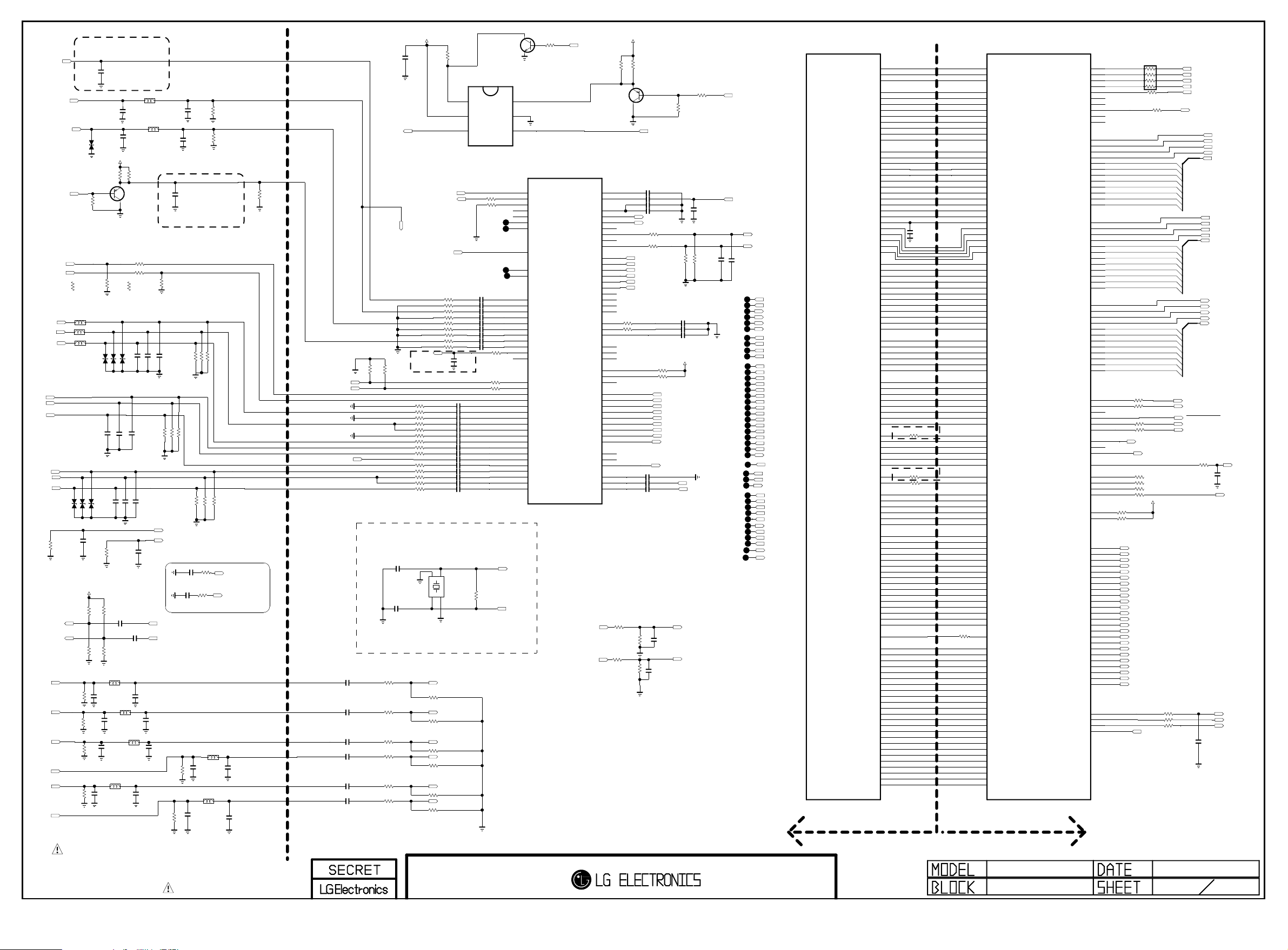
Place these close to tuner
Copyright ⓒ 2012 LG Electronics. Inc. All right reserved.
Only for training and service purposes
LGE Internal Use Only
TU_CVBS
680pF
C506
OPT
L503
SC_CVBS_IN
AV1_CVBS_IN
DSUB_B+
DSUB_G+
DSUB_R+
SC_B
SC_G
SC_R
COMP1_Pb
COMP1_Y
COMP1_Pr
OPT
R3634
SCART_Lout
SCART_Rout
PC_L_IN
PC_R_IN
SC_L_IN
SC_R_IN
AV1_L_IN
AV1_R_IN
CHB_CVBS
2K
SC_FB
SC_ID
C3625
470K
D503
5.5V
5pF
50V
R601
470K
R607
EU
R602
470K
R603
470K
R617
L501
L500
L502
OPT
D504
5.5V
75
OPT
NON SCART
R525-*1
0
D506
D505
5.5V
5.5V
OPT
R3633
+12V
100K
100K
2K
R552
R554
OPT
Q505
CHB
D500
5.5V
C528
EU
EU
C573
560pF
50V
C574
560pF
50V
OPT
+5V_TU
R618
220
CHB
B
5.5V
OPT
OPT
10pF
100K
100K
L506
OPT
C572
330pF
50V
L508
EU
R525
75
D501
OPT
C546
C580
10pF
R538
2.2uF
10V
R549
C581
560pF
50V
OPT
5.5V
OPT
10pF
EU
EU
C525
EU
E
C
R522
D502
OPT
C579
C3626
L509
EU
1uH
C508
EU
150pF
50V
EU
L504
1uH
50V
150pF
C511
R616
220
CHB
680pF
C517
OPT
R521 100
10K
EU
EU
NON SCART
R524
R524-*1
2.7K
0
OPT
OPT
OPT
C606
10pF
C605
C607
10pF
10pF
75
75
75
R595
R600
R594
DSUB_VSYNC
DSUB_HSYNC
Near Place Scart AMP
C6006
1uF 25V
C6001
SCART_Lout_SOC
SCART_Rout_SOC
C587
100pF
50V
C576
330pF
50V
EU
EU
R608
470K
R609
470K
C524
10pF
5pF
50V
OPT
2.2uF
L507
10pF
10V
OPT
C578
C522
EU
10pF
C575
100pF
50V
C577
100pF
50V
Place JACK Side
C514
150pF
50V
EU
1uF25V
EU
C509
150pF
EU
75
R52 8
75
1%
R606
C586
560pF
50V
OPT
75
R52 9
EU
10K
R60 06
EU
10K
R6005
C582
330pF
50V
OPT
75
1%
R605
L511
R53 0
75
EU
L510
75
1%
R604
R614
75
1%
R615
75
1%
SCART_AMP_R_FB
SCART_AMP_L_FB
EU
C588
330pF
50V
C589
100pF
50V
DTV/MNT_V_OUT
R613
75
OPT
1%
SC_SOG_IN
10K
10K
R555
DSUB_HSYNC
DSUB_VSYNC
SC_SOG_IN
R553
Main clock for LG1152A
8pF
C513
8pF
C512
C500
R508 22K
2.2uF
C501
R509 22K
2.2uF
EU
EU
2.2uF
2.2uF
2.2uF
2.2uF
R510
EU
R511
EU
R512 22K
R513 22K
22K
22K
C502
C503
C504
C505
Place SOC Side
THE SYMBOL MARK OF THIS SCHEMETIC DIAGRAM INCORPORATES
SPECIAL FEATURES IMPORTANT FOR PROTECTION FROM X-RADIATION.
FILRE AND ELECTRICAL SHOCK HAZARDS, WHEN SERVICING IF IS
ESSENTIAL THAT ONLY MANUFATURES SPECFIED PARTS BE USED FOR
THE CRITICAL COMPONENTS IN THE SYMBOL MARK OF THE SCHEMETIC.
+5V_NORMAL
EU
C510
0.1uF
16V
DTV/MNT_VOUT
Close to LG1152A
R536 68
R539 33
R541 68
R546 33
R547 0
R548 68
R550 33
R568 33
R569 33
R570 33
R564 150
R565 150
R566 0
R567 150
R514 75K
R515 100K
R516 75K
R517 100K
R518 75K
R519 100K
EU
R527
10K
SELECT
XIN_SUB
XO_SUB
SOC_RESET
R571 33
R572 33
R573 100
R559 68
R574 100
R551 33
R557 33
R575 33
R558 68
C516 0.047uF
C518 0.047uF
C523 0.047uF
C526 0.047uF
C527 1000pF
C531 0.047uF
C532 0.047uF
C542 0.047uF
C543 0.047uF
C544 1000pF
C545 0.047uF
C538 0.047uF
C539 0.047uF
C540 1000pF
C541 0.047uF
X-TAL_1
GND_1
1
2
X500
24MHz
4
3
GND_2
X-TAL_2
AUAD_L_CH5_IN
AUAD_R_CH5_IN
AUAD_L_CH4_IN
EU
AUAD_R_CH4_IN
EU
AUAD_L_CH3_IN
AUAD_R_CH3_IN
Q506
MMBT3904(NXP)
IC500
NLASB3157DFT2G
EU
R560
R561
0.047uF
0.047uF
0.047uF
0.047uF
0.047uF
0.047uF
0.047uF
0.047uF
0.047uF
R563 0
EU
22
22
1M
1
2
3
330
33
XIN_SUB
XO_SUB
6
VCC
5
A
4
Selece = High ==> A = B1
Selece = Low ==> A = B0
C549
C550
C551
C552
C553
C554
C555
C556
C557
C515
100pF
50V
EU
R579
R580
R535
C
E
B1
GND
B0
L17
L18
P17
K17
K18
M2
M1
R4
N3
M3
U14
T14
V15
U15
T15
U16
V14
T16
V16
V17
U17
P8
R8
P11
R11
U8
V8
V10
T8
V9
T11
U9
T9
U10
T10
V11
U11
V12
U12
T12
EU
XIN_SUB
XO_SUB
VSB_AUX_XIN
XTLIN_AAD
XTLOUT_AAD
OPM1
OPM0
PORES_N
L9A_SCL
L9A_SDA
CVBS_IN1
CVBS_IN2
CVBS_IN3
CVBS_VCM
CVBS_IN4
CVBS_IN5
CVBS_IN6
CB_IN
CB_VCM
BUF_OUT1
BUF_OUT2
HSYNC
VSYNC
SC1_FB
SC1_SID
BINCOM_IN
B_IN
GINCOM_IN
G_IN
SOG_IN
RINCOM_IN
R_IN
PB1_IN
Y1_IN
SOY1_IN
PR1_IN
PB2_IN
Y2_IN
SOY2_IN
PR2_IN
B
EU
R507
10K
IC101
LG1152AN-B2
AAD_ADC_SIFM
AAD_ADC_SIF
AUDA_BGR_OUT
AUD_SCART0_OUTLN
AUD_SCART0_OUTLP
AUD_SCART0_OUTRN
AUD_SCART0_OUTRP
AUAD_L_CH5_IN
AUAD_R_CH5_IN
AUAD_L_CH4_IN
AUAD_R_CH4_IN
AUAD_L_CH3_IN
AUAD_R_CH3_IN
AUAD_L_CH2_IN
AUAD_R_CH2_IN
AUAD_L_CH1_IN
AUAD_R_CH1_IN
AUAD_VR_OUT
PHY0_RXCN_0
PHY0_RXCP_0
PHY0_RX0N_0
PHY0_RX0P_0
PHY0_RX1N_0
PHY0_RX1P_0
PHY0_RX2N_0
PHY0_RX2P_0
PHY0_ARC_OUT_0
ADC_I_INCOM
AUDA_OUTR
DTV_ATV_SELECT
AUDA_OUTL
AUDA_OUTR
AUAD_REFN
AUAD_REFP
AUMI_BIAS
AUMI_IN
AUMI_COM
DDCD0_DA
DDCD0_CK
HPD0
ANTCON
RFAGC
IFAGC
ADC_I_INP
ADC_I_INN
AUDA_OUTL
+5V_NORMAL
R592
220
EU
EU
Q504
MMBT3906(NXP)
N17
N18
U1
R1
R2
T1
V2
U2
T2
U3
V3
V4
T3
U5
T5
U6
T6
U7
T7
T4
10K
U4
V5
R7
R5
R6
E18
E17
E16
J18
J17
H17
H18
G17
G18
G16
F16
F17
P12
M18
P18
T17
U18
T18
R624
100
R625
100
R593
220
EU
E
B
C
DTV/MNT_VOUT
C533 0.1uF
C534 0.1uF
10uFC535
C536 2.2uF
AUDA_OUTL
AUDA_OUTR
EU
EU
AUAD_L_CH5_IN
AUAD_R_CH5_IN
AUAD_L_CH4_IN
AUAD_R_CH4_IN
AUAD_L_CH3_IN
AUAD_R_CH3_IN
R534
R52010K
R577 4.7K
R578 4.7K
0.1uF
C115
0.1uF
C116
0.1uF
C117
H/NIM&CHB
H/NIM&CHB
R626
22K
C604
0.01uF
R627
22K
R599
75
R501100
R502100
+3.3V_NORMAL
HDMI_CLKHDMI_CLK+
HDMI_RX0HDMI_RX0+
HDMI_RX1HDMI_RX1+
HDMI_RX2HDMI_RX2+
SPDIF_OUT_ARC
IF_AGC
C603
0.01uF
EU
OPT
C558
1000pF
OPT
22K
EU
EU
R531
R532 22K
C5372.2uF
C5472.2uF
C5482.2uF
IF_N
IF_P
HP_LOUT_MAIN
HP_ROUT_MAIN
IC101
LG1152AN-B2
L1
INTR_GBB
BB_TP_VAL
BB_TP_SOP
BB_TP_ERR
BB_TP_CLK
BB_SDA_I
BB_SDA_O
BB_SCL
L9DA_SCL
CHB_DN
CHB_UP
CHB_START
CHB_DATA0
CHB_DATA1
CHB_DATA2
CHB_DATA3
CHB_DATA4
CLK_F54M
CVBS_GC2
CVBS_GC1
CVBS_GC0
CVBS_UP
CVBS_DN
FS00CLK
DAC_DATA0
DAC_DATA1
DAC_DATA2
DAC_DATA3
DAC_DATA4
DAC_START
AAD_GC0
AAD_GC1
AAD_GC2
AAD_GC3
AAD_GC4
AAD_DATA0
AAD_DATA1
AAD_DATA2
AAD_DATA3
AAD_DATA4
AAD_DATA5
AAD_DATA6
AAD_DATA7
AAD_DATA8
AAD_DATA9
HSR_AM0
HSR_AP0
HSR_BM0
HSR_BP0
HSR_CM0
HSR_CP0
HSR_CLKM0
HSR_CLKP0
HSR_DM0
HSR_DP0
HSR_EM0
HSR_EP0
HSR_AM1
HSR_AP1
HSR_BM1
HSR_BP1
HSR_CM1
HSR_CP1
HSR_CLKM1
HSR_CLKP1
HSR_DM1
HSR_DP1
HSR_EM1
HSR_EP1
L2
L3
K1
K2
J2
J3
K3
H1
H2
H3
J1
G1
G2
G3
B1
C1
A4
B4
C4
A2
D1
D2
E2
E1
F1
F2
B2
A3
C2
B3
C3
D3
E3
F3
D4
E4
F4
D5
E5
F5
D6
A5
B5
C5
A6
B6
C6
E6
F6
D7
B7
C7
A8
B8
C8
Close to LG1152A
A7
R581 33
D8
F7
E7
E8
F8
Close to LG1152A
A9
R582 33
B9
R583 33
C9
D9
E9
F9
C10
D10
E10
F10
D11
E11
F11
D12
E12
F12
D13
E13
F13
D14
E14
F14
D15
E15
F15
B10
A10
A11
B11
C12
C11
B12
A12
A13
B13
C14
C13
B14
A14
A15
B15
C16
C15
B16
A16
A17
B17
C18
C17
C529
220pF
OPT
50V
INTR_HDMI1
R576100
ATV_OUT
TUNER_SIF
SCART_Lout_SOC
SCART_Rout_SOC
EU
EU
C520 0.01uF
C521 0.01uF
TPI_SOP
TPI_CLK
TPO_ERR
TPO_VAL
TPO_SOP
TPO_CLK
CHB_DATA
JDVR_SCLK
CHB_VAL
CHB_ERR
TU_CVBS
SCART_Lout
SCART_Rout
SC_R
CHB_CVBS
SC_CVBS_IN
SC_B
SC_G
SC_FB
SC_ID
ATV_OUT
SC_L_IN
SC_R_IN
TUNER_SIF
TUNER_SIF
DTV/MNT_V_OUT
JDVR_SCLK
IF_N
IF_P
IF_AGC
FE_TS_CLK
FE_TS_SYNC
FE_TS_VAL
TPI_DVB_ERR
FE_TS_DATA[0-7]
TPO_DATA[0-7]
TPI_DATA[0-7]
TPI_ERR
TPI_VAL
OPTIC_GPIO1
OPTIC_BACK_CHANNEL
INTR_AFE3CH
AUD_HMR00ARC
AUD_HMR0AMUTE
AUD_HMR0ALRCK
AUD_HMR0ABCK
AUD_HMR0ASD4
AUD_HMR0ASD3
AUD_HMR0ASD2
AUD_HMR0ASD1
AUD_HMR0ASD0
AUD_DAC1_LRCH
AUD_DAC1_SCK
AUD_DAC1_LRCK
AUD_FS25CLK
AUD_FS24CLK
AUD_FS23CLK
AUD_FS21CLK
AUD_FS20CLK
AUDCLK_OUT_SUB
AUD_DAC0_LRCK
AUD_DAC0_LRCH
AUD_DAC0_SCK
AUD_ADC_LRCH
AUD_ADC_SCK
AUD_ADC_LRCK
AUD_MIC_LRCH
AUD_MIC_SCK
AUD_MIC_LRCK
BB_TP_DATA0
BB_TP_DATA1
BB_TP_DATA2
BB_TP_DATA3
BB_TP_DATA4
BB_TP_DATA5
BB_TP_DATA6
BB_TP_DATA7
L9DA_SDA_I
L9DA_SDA_O
AUDCLK_OUT
AAD_DATAEN
DCO_OUT_CLK
R9112
33
AH2
INTR_GBB
AG2
INTR_HDMI1
AF2
INTR_AFE3CH
AH3
AUD_HMR0ARC
AG3
AUD_HMR0AMUTE
AG4
AUD_HMR0ALRCK
AF4
AUD_HMR0ABCK
AF3
AUD_HMR0ASD4
AH5
AUD_HMR0ASD3
AG5
AUD_HMR0ASD2
AF5
AUD_HMR0ASD1
AH4
AUD_HMR0ASD0
AH6
AUD_DAC1_LRCH
AG6
AUD_DAC1_SCK
AF6
AUD_DAC1_LRCK
AH7
AUD_FS25CLK
AG7
AUD_FS24CLK
AH10
AUD_FS23CLK
AG10
AUD_FS21CLK
AF10
AUD_FS20CLK
AH8
AUDCLK_OUT_SUB
AF7
AUD_DAC0_LRCK
AE8
AUD_DAC0_LRCH
AD8
AUD_DAC0_SCK
AE7
AUD_ADC_LRCH
AD7
AUD_ADC_SCK
AC8
AUD_ADC_LRCK
AG8
AUD_MIC_LRCH
AH9
AUD_MIC_SCK
AF8
AUD_MIC_LRCK
AG9
BB_TPI_DATA0
AF9
BB_TPI_DATA1
AE9
BB_TPI_DATA2
AD9
BB_TPI_DATA3
AC9
BB_TPI_DATA4
AE10
BB_TPI_DATA5
AD10
BB_TPI_DATA6
AC10
BB_TPI_DATA7
AE11
BB_TPI_VAL
AD11
BB_TPI_SOP
AC11
BB_TPI_ERR
AE12
BB_TPI_CLK
AH11
BB_SDA_I
AG11
BB_SDA_O
AF11
BB_SCL
AH12
HS_SCL
AG12
HS_SDA_I
AF12
HS_SDA_O
AD12
CHB_DN
AC12
CHB_UP
AE13
CHB_START
AG13
CHB_DATA0
AF13
CHB_DATA1
AH14
CHB_DATA2
AG14
CHB_DATA3
AF14
CHB_DATA4
AH13
CLK_54
AE14
CVBS_GC2
AC13
CVBS_GC1
AD13
CVBS_GC0
AD14
CVBS_UP
AC14
CVBS_DN
AH15
FS00CLK
AG15
AUDCLK_TO_DIGITAL
AF15
DAC_DATA0
AE15
DAC_DATA1
AD15
DAC_DATA2
AC15
DAC_DATA3
AF16
DAC_DATA4
AE16
DAC_START
AD16
AAD_GC0
AC16
AAD_GC1
AE17
AAD_GC2
AD17
AAD_GC3
AC17
AAD_GC4
AE18
AAD_DATAEN
AD18
AAD_DATA0
AC18
AAD_DATA1
AE19
AAD_DATA2
AD19
AAD_DATA3
AC19
AAD_DATA4
AE20
AAD_DATA5
AD20
AAD_DATA6
AC20
AAD_DATA7
AE21
AAD_DATA8
AD21
AAD_DATA9
AC21
AUPLL_CLK
AG16
HS_RX1_AM
AH16
HS_RX1_AP
AH17
HS_RX1_BM
AG17
HS_RX1_BP
AF18
HS_RX1_CM
AF17
HS_RX1_CP
AG18
HS_RX1_CLKM
AH18
HS_RX1_CLKP
AH19
HS_RX1_DM
AG19
HS_RX1_DP
AF20
HS_RX1_EM
AF19
HS_RX1_EP
AG20
HS_RX2_AM
AH20
HS_RX2_AP
AH21
HS_RX2_BM
AG21
HS_RX2_BP
AF22
HS_RX2_CM
AF21
HS_RX2_CP
AG22
HS_RX2_CLKM
AH22
HS_RX2_CLKP
AH23
HS_RX2_DM
AG23
HS_RX2_DP
AF24
HS_RX2_EM
AF23
HS_RX2_EP
IC100
LG1152D-B1
STPIO_SOP/GPIO43
STPIO_VAL/GPIO42
STPIO_ERR/GPIO41
STPIO_DATA/GPIO40
TPI_DVB_CLK/GPIO47
TPI_DVB_SOP/GPIO46
TPI_DVB_VAL/GPIO45
TPI_DVB_DATA0/GPIO44
PCMI3LRCK/GPIO81
AUD_SUBSCK/GPIO51
AUD_SUBLRCK/GPIO52
STPI_CLK
STPI_SOP
STPI_VAL
STPI_ERR
STPI_DATA
STPIO_CLK
TPI_DVB_ERR
TPI_DVB_DATA1
TPI_DVB_DATA2
TPI_DVB_DATA3
TPI_DVB_DATA4
TPI_DVB_DATA5
TPI_DVB_DATA6
TPI_DVB_DATA7
TPI_CLK
TPI_SOP
TPI_VAL
TPI_ERR
TPI_DATA0
TPI_DATA1
TPI_DATA2
TPI_DATA3
TPI_DATA4
TPI_DATA5
TPI_DATA6
TPI_DATA7
TPO_CLK
TPO_SOP
TPO_VAL
TPO_ERR
TPO_DATA0
TPO_DATA1
TPO_DATA2
TPO_DATA3
TPO_DATA4
TPO_DATA5
TPO_DATA6
TPO_DATA7
AUDCLK_OUT
DACLRCH
DACSLRCH/GPIO95
DACCLFCH/GPIO94
DACSCK
DACLRCK
PCMI3LRCH
PCMI3SCK/GPIO80
IEC958OUT
AUD_SUBMCK
AUD_SUBLRCH
BTSCSEL
DTS_EN
TXA0N
TXA0P
TXA1N
TXA1P
TXA2N
TXA2P
TXACLKN
TXACLKP
TXA3N
TXA3P
TXA4N
TXA4P
TXB0N
TXB0P
TXB1N
TXB1P
TXB2N
TXB2P
TXBCLKN
TXBCLKP
TXB3N
TXB3P
TXB4N
TXB4P
PWM0/GPIO55
PWM1/GPIO54
PWM2/GPIO53
PWM_IN
AR102
CHB
AE27
AE26
AD28
AD27
AD26
AC28
AC26
AB28
AC27
AB27
AF27
AE28
AG27
AF28
AG26
AF26
AF25
AH26
AH25
AG25
AH24
AG24
H24
J25
J24
H25
J27
J26
H28
H27
H26
G28
G27
G26
D24
E23
D25
D23
H23
G25
G24
F25
F24
F23
E25
E24
C1
C2
A3
A2
B2
B1
B3
C3
A4
AE2
AD25
AC25
AD24
AE25
AB18
AB19
DTS_EN: ENABLE(’1’) (for development)
BTSC_EN: ENABLE(’1’) (for development)
N1
N2
P2
P1
P3
R3
R1
R2
T2
T1
T3
U3
U1
U2
V2
V1
V3
W3
W1
W2
Y2
Y1
Y3
AA3
L6
L5
M4
M5
47
R200
47
FE_TS_DATA[0]
FE_TS_DATA[1]
FE_TS_DATA[2]
FE_TS_DATA[3]
FE_TS_DATA[4]
FE_TS_DATA[5]
FE_TS_DATA[6]
FE_TS_DATA[7]
R542100
100
100
100
OPTIC_BACK_CHANNEL
R598 47
OPT
R619 47
OPT
R628 22
OPT
R629 47
+3.3V_NORMAL
R59622
R59722
SOC_TXA0N
SOC_TXA0P
SOC_TXA1N
SOC_TXA1P
SOC_TXA2N
SOC_TXA2P
SOC_TXACLKN
SOC_TXACLKP
SOC_TXA3N
SOC_TXA3P
SOC_TXA4N
SOC_TXA4P
SOC_TXB0N
SOC_TXB0P
SOC_TXB1N
SOC_TXB1P
SOC_TXB2N
SOC_TXB2P
SOC_TXBCLKN
SOC_TXBCLKP
SOC_TXB3N
SOC_TXB3P
SOC_TXB4N
SOC_TXB4P
OPT
EDGE_LED
BPL_IN
CHB
33
R556
TPI_DATA[0]
TPI_DATA[1]
TPI_DATA[2]
TPI_DATA[3]
TPI_DATA[4]
TPI_DATA[5]
TPI_DATA[6]
TPI_DATA[7]
TPO_DATA[0]
TPO_DATA[1]
TPO_DATA[2]
TPO_DATA[3]
TPO_DATA[4]
TPO_DATA[5]
TPO_DATA[6]
TPO_DATA[7]
R543
R544
R545
OPTIC_GPIO1
R631
R632
R633
R630 100
10K
100
100
CHB_CLK
CHB_SYNC
CHB_VAL
CHB_ERR
CHB_DATA
USB_CTL2
FE_TS_CLK
FE_TS_SYNC
FE_TS_VAL
TPI_DVB_ERR
FE_TS_DATA[0-7]
TPI_CLK
TPI_SOP
TPI_VAL
TPI_ERR
TPI_DATA[0-7]
TPO_CLK
TPO_SOP
TPO_VAL
TPO_ERR
TPO_DATA[0-7]
AUD_MASTER_CLK
AUD_LRCH
FRC3_FLASH_WP
AUD_SCK
AUD_LRCK
C559
OPT
2.2uF
C630
82pF
50V
AMP_RESET_N
A_DIM
PWM_DIM2
PWM_DIM
SPDIF_OUT
LG1152A LG1152D
LG1152 B0
MAIN AUDIO/VIDEO
3
Page 22
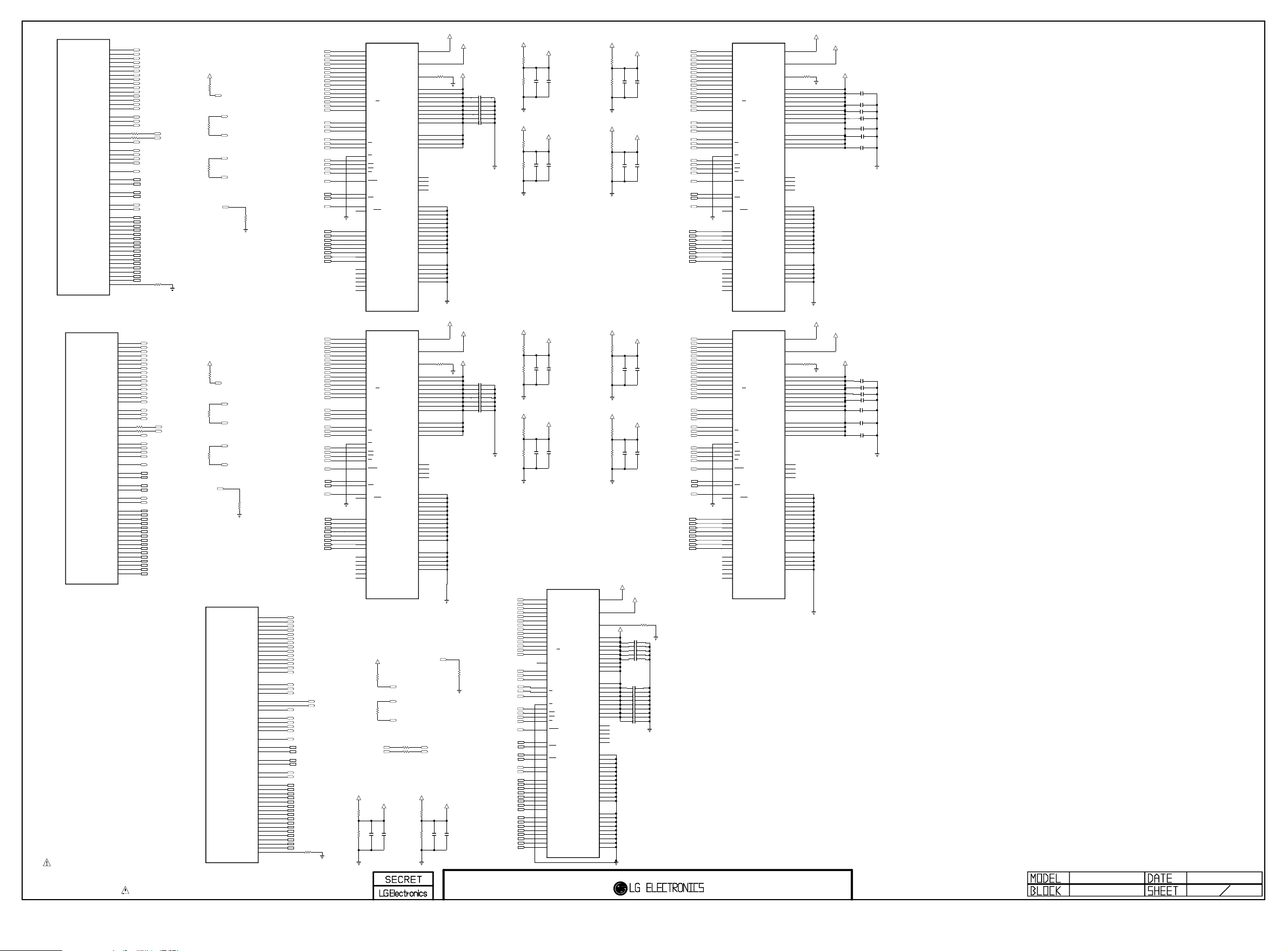
IC100
Copyright ⓒ 2012 LG Electronics. Inc. All right reserved.
Only for training and service purposes
LGE Internal Use Only
LG1152D-B1
M0_DDR_RESET_N
M0_DDR_DQSL_P
M0_DDR_DQSL_N
M0_DDR_DQSU_P
M0_DDR_DQSU_N
M0_DDR_ZQCAL
M0_DDR_A0
M0_DDR_A1
M0_DDR_A2
M0_DDR_A3
M0_DDR_A4
M0_DDR_A5
M0_DDR_A6
M0_DDR_A7
M0_DDR_A8
M0_DDR_A9
M0_DDR_A10
M0_DDR_A11
M0_DDR_A12
M0_DDR_A13
M0_DDR_A14
M0_DDR_BA0
M0_DDR_BA1
M0_DDR_BA2
M0_DDR_CLK
M0_DDR_CLKN
M0_DDR_CKE
M0_DDR_ODT
M0_DDR_RASN
M0_DDR_CASN
M0_DDR_WEN
M0_DDR_DML
M0_DDR_DMU
M0_DDR_DQ0
M0_DDR_DQ1
M0_DDR_DQ2
M0_DDR_DQ3
M0_DDR_DQ4
M0_DDR_DQ5
M0_DDR_DQ6
M0_DDR_DQ7
M0_DDR_DQ8
M0_DDR_DQ9
M0_DDR_DQ10
M0_DDR_DQ11
M0_DDR_DQ12
M0_DDR_DQ13
M0_DDR_DQ14
M0_DDR_DQ15
D18
E17
E18
E20
E16
D20
F16
F19
E15
D19
D14
E14
D17
F18
D16
F20
D15
F17
A17
A18
F15
F21
D22
E21
D21
E19
B20
A20
B16
C16
C19
C15
C20
B19
C21
B18
A21
C18
B21
A19
B17
C14
A16
B14
B15
A14
C17
A15
E22
R700 0
R701 0
SIGN50005
M0_DDR_A0
M0_DDR_A1
M0_DDR_A2
M0_DDR_A3
M0_DDR_A4
M0_DDR_A5
M0_DDR_A6
M0_DDR_A7
M0_DDR_A8
M0_DDR_A9
M0_DDR_A10
M0_DDR_A11
M0_DDR_A12
M0_DDR_A13
M0_DDR_A14
M0_DDR_BA0
M0_DDR_BA1
M0_DDR_BA2
M0_DDR_CKE
M0_DDR_ODT
M0_DDR_RASN
M0_DDR_CASN
M0_DDR_WEN
M0_DDR_RESET_N
M0_DDR_DQSL_P
M0_DDR_DQSL_N
M0_DDR_DQSU_P
M0_DDR_DQSU_N
M0_DDR_DML
M0_DDR_DMU
M0_DDR_DQ0
M0_DDR_DQ1
M0_DDR_DQ2
M0_DDR_DQ3
M0_DDR_DQ4
M0_DDR_DQ5
M0_DDR_DQ6
M0_DDR_DQ7
M0_DDR_DQ8
M0_DDR_DQ9
M0_DDR_DQ10
M0_DDR_DQ11
M0_DDR_DQ12
M0_DDR_DQ13
M0_DDR_DQ14
M0_DDR_DQ15
240
1%
M0_DDR_CLK
M0_DDR_CLKN
R704
VCC1.5V_MAIN
R709
10K
R705
200
R706
200
M0_DDR_CKE
M0_DDR_RESET_N
M0_DDR_CLK
M0_DDR_CLKN
M0_DDR_CLK
M0_DDR_CLKN
IC700
H5TQ2G83BFR-PBC
DDR3
K4
M0_DDR_A0
M0_DDR_A1
M0_DDR_A2
M0_DDR_A3
M0_DDR_A4
M0_DDR_A5
M0_DDR_A6
M0_DDR_A7
M0_DDR_A8
M0_DDR_A9
M0_DDR_A10
M0_DDR_A11
M0_DDR_A12
M0_DDR_A13
M0_DDR_A14
M0_DDR_BA0
M0_DDR_BA1
M0_DDR_BA2
M0_DDR_CLK
M0_DDR_CLKN
M0_DDR_CKE
M0_DDR_ODT
M0_DDR_RASN
M0_DDR_CASN
M0_DDR_WEN
M0_DDR_RESET_N
M0_DDR_DQSL_P
M0_DDR_DQSL_N
R742
10K
M0_DDR_DML
M0_DDR_DQ0
M0_DDR_DQ1
M0_DDR_DQ6
M0_DDR_DQ4
M0_DDR_DQ3
M0_DDR_DQ2
M0_DDR_DQ5
2Gbit
A0
L8
A1
L4
A2
K3
A3
L9
A4
L3
A5
M9
A6
M3
A7
N9
A8
M4
A9
H8
A10/AP
M8
A11
K8
A12/BC
N4
A13
N8
A14
J3
BA0
K9
BA1
J4
BA2
F8
CK
G8
CK
G10
CKE
H3
CS
G2
ODT
F4
RAS
G4
CAS
H4
WE
N3
RESET
C4
DQS
D4
DQS
B8
DM/TDQS
A8
NF/TDQS
B4
DQ0
C8
DQ1
C3
DQ2
C9
DQ3
E4
DQ4
E9
DQ5
D3
DQ6
E8
DQ7
A4
NC_1
F2
NC_2
F10
NC_3
H2
NC_4
H10
NC_5
J8
NC_6
VREFCA
VREFDQ
VDDQ_1
VDDQ_2
VDDQ_3
VDDQ_4
VSS_10
VSS_11
VSS_12
VSSQ_1
VSSQ_2
VSSQ_3
VSSQ_4
VSSQ_5
VDD_1
VDD_2
VDD_3
VDD_4
VDD_5
VDD_6
VDD_7
VDD_8
VDD_9
NC_S1
NC_S2
NC_S3
NC_S4
VSS_1
VSS_2
VSS_3
VSS_4
VSS_5
VSS_6
VSS_7
VSS_8
VSS_9
M0_DDR_VREFCA
M0_DDR_VREFDQ
J9
E2
VCC1.5V_MAIN
R720
H9
ZQ
240
1%
A3
A10
D8
G3
G9
K2
K10
M2
M10
B10
C2
E3
E10
A1
A11
N1
N11
A2
A9
B2
D9
F3
F9
J2
J10
L2
L10
N2
N10
B3
B9
C10
D2
D10
C706 0.1uF
C707
C708
C709
C710
C711
C712
0.1uF
0.1uF
0.1uF
0.1uF
0.1uF
0.1uF
VCC1.5V_MAIN
R722
1K 1%
R723
1K 1%
VCC1.5V_MAIN
R724
1K 1%
R725
1K 1%
M0_DDR_VREFCA
0.1uF
C724
M0_DDR_VREFDQ
0.1uF
C725
VCC1.5V_MAIN
M0_1_DDR_VREFCA
R730
1K 1%
1000pF
C728
1000pF
C729
R731
1K 1%
VCC1.5V_MAIN
R732
R733
1K 1%
C732
M0_1_DDR_VREFDQ
1K 1%
C733
0.1uF
C747
0.1uF
C748
1000pF
1000pF
M0_DDR_A0
M0_DDR_A1
M0_DDR_A2
M0_DDR_A3
M0_DDR_A4
M0_DDR_A5
M0_DDR_A6
M0_DDR_A7
M0_DDR_A8
M0_DDR_A9
M0_DDR_A10
M0_DDR_A11
M0_DDR_A12
M0_DDR_A13
M0_DDR_A14
M0_DDR_BA0
M0_DDR_BA1
M0_DDR_BA2
M0_DDR_CLK
M0_DDR_CLKN
M0_DDR_CKE
M0_DDR_ODT
M0_DDR_RASN
M0_DDR_CASN
M0_DDR_WEN
M0_DDR_RESET_N
M0_DDR_DQSU_P
M0_DDR_DQSU_N
M0_DDR_DMU
M0_DDR_DQ10
M0_DDR_DQ13
M0_DDR_DQ14
M0_DDR_DQ11M0_DDR_DQ7
M0_DDR_DQ15
M0_DDR_DQ9
M0_DDR_DQ8
M0_DDR_DQ12
H5TQ2G83BFR-PBC
K4
A0
L8
A1
L4
A2
K3
A3
L9
A4
L3
A5
M9
A6
M3
A7
N9
A8
M4
A9
H8
A10/AP
M8
A11
K8
A12/BC
N4
A13
N8
A14
J3
BA0
K9
BA1
J4
BA2
F8
CK
G8
CK
G10
CKE
H3
CS
G2
ODT
F4
RAS
G4
CAS
H4
WE
N3
RESET
C4
DQS
D4
DQS
B8
DM/TDQS
A8
NF/TDQS
B4
DQ0
C8
DQ1
C3
DQ2
C9
DQ3
E4
DQ4
E9
DQ5
D3
DQ6
E8
DQ7
A4
NC_1
F2
NC_2
F10
NC_3
H2
NC_4
H10
NC_5
J8
NC_6
IC703
DDR3
2Gbit
VREFCA
VREFDQ
VDD_1
VDD_2
VDD_3
VDD_4
VDD_5
VDD_6
VDD_7
VDD_8
VDD_9
VDDQ_1
VDDQ_2
VDDQ_3
VDDQ_4
NC_S1
NC_S2
NC_S3
NC_S4
VSS_1
VSS_2
VSS_3
VSS_4
VSS_5
VSS_6
VSS_7
VSS_8
VSS_9
VSS_10
VSS_11
VSS_12
VSSQ_1
VSSQ_2
VSSQ_3
VSSQ_4
VSSQ_5
M0_1_DDR_VREFCA
J9
E2
H9
ZQ
A3
A10
D8
G3
G9
K2
K10
M2
M10
B10
C2
E3
E10
A1
A11
N1
N11
A2
A9
B2
D9
F3
F9
J2
J10
L2
L10
N2
N10
B3
B9
C10
D2
D10
M0_1_DDR_VREFDQ
R739
240
1%
VCC1.5V_MAIN
C758
C746
C723
C760
C751
C756
0.1uF
0.1uF
0.1uF
0.1uF
0.1uF
0.1uF
C761
0.1uF
IC100
LG1152D-B1
C9
E9
F10
F12
F8
D11
E8
E11
E7
D10
C4
C5
D8
E10
C7
E12
F7
D9
A9
B9
D7
D13
C13
E13
D12
F11
C12
C11
A7
B7
A11
C6
A12
B11
A13
C10
B12
A10
B13
B10
A8
B4
C8
B5
B6
A5
B8
A6
R702 0
R703 0
M1_DDR_A0
M1_DDR_A1
M1_DDR_A2
M1_DDR_A3
M1_DDR_A4
M1_DDR_A5
M1_DDR_A6
M1_DDR_A7
M1_DDR_A8
M1_DDR_A9
M1_DDR_A10
M1_DDR_A11
M1_DDR_A12
M1_DDR_A13
M1_DDR_A14
M1_DDR_BA0
M1_DDR_BA1
M1_DDR_BA2
M1_DDR_CLK
M1_DDR_CLKN
M1_DDR_CKE
M1_DDR_ODT
M1_DDR_RASN
M1_DDR_CASN
M1_DDR_WEN
M1_DDR_RESET_N
M1_DDR_DQSL_P
M1_DDR_DQSL_N
M1_DDR_DQSU_P
M1_DDR_DQSU_N
M1_DDR_DML
M1_DDR_DMU
M1_DDR_DQ0
M1_DDR_DQ1
M1_DDR_DQ2
M1_DDR_DQ3
M1_DDR_DQ4
M1_DDR_DQ5
M1_DDR_DQ6
M1_DDR_DQ7
M1_DDR_DQ8
M1_DDR_DQ9
M1_DDR_DQ10
M1_DDR_DQ11
M1_DDR_DQ12
M1_DDR_DQ13
M1_DDR_DQ14
M1_DDR_DQ15
VCC1.5V_MAIN
M1_DDR_CKE
R710
10K
M1_DDR_RESET_N
M1_DDR_CLK
R707
200
M1_DDR_CLKN
M1_DDR_CLK
R708
200
M1_DDR_CLKN
IC100
LG1152D-B1
R741
10K
M2_DDR_A0
M2_DDR_A1
M2_DDR_A2
M2_DDR_A3
M2_DDR_A4
M2_DDR_A5
M2_DDR_A6
M2_DDR_A7
M2_DDR_A8
M2_DDR_A9
M2_DDR_A10
M2_DDR_A11
M2_DDR_A12
M2_DDR_A13
M2_DDR_BA0
M2_DDR_BA1
M2_DDR_BA2
M2_DDR_CLK
M2_DDR_CLKN
M2_DDR_CKE
M2_DDR_ODT
M2_DDR_RASN
M2_DDR_CASN
M2_DDR_WEN
M2_DDR_RESET_N
M2_DDR_DQSU_P
M2_DDR_DQSU_N
M2_DDR_DQSL_P
M2_DDR_DQSL_N
M2_DDR_DML
M2_DDR_DMU
M2_DDR_DQ0
M2_DDR_DQ1
M2_DDR_DQ2
M2_DDR_DQ3
M2_DDR_DQ4
M2_DDR_DQ5
M2_DDR_DQ6
M2_DDR_DQ7
M2_DDR_DQ8
M2_DDR_DQ9
M2_DDR_DQ10
M2_DDR_DQ11
M2_DDR_DQ12
M2_DDR_DQ13
M2_DDR_DQ14
M2_DDR_DQ15
M2_DDR_ZQCAL
M1_DDR_RESET_N
M1_DDR_DQSL_P
M1_DDR_DQSL_N
D1
K4
D2
E5
H6
E4
J4
D6
J5
D3
H4
J6
K5
D4
E6
H5
F4
M2
M3
G6
F6
G5
G4
F5
D5
H3
J1
H1
H2
K3
F2
F1
L1
E3
L2
E1
M1
E2
L3
J3
G1
K2
F3
J2
G2
K1
G3
K6
M2_DDR_A0
M2_DDR_A1
M2_DDR_A2
M2_DDR_A3
M2_DDR_A4
M2_DDR_A5
M2_DDR_A6
M2_DDR_A7
M2_DDR_A8
M2_DDR_A9
M2_DDR_A10
M2_DDR_A11
M2_DDR_A12
M2_DDR_A13
M2_DDR_BA0
M2_DDR_BA1
M2_DDR_BA2
M2_DDR_CKE
M2_DDR_ODT
M2_DDR_RASN
M2_DDR_CASN
M2_DDR_WEN
M2_DDR_RESET_N
M2_DDR_DQSU_P
M2_DDR_DQSU_N
M2_DDR_DQSL_P
M2_DDR_DQSL_N
M2_DDR_DML
M2_DDR_DMU
M2_DDR_DQ0
M2_DDR_DQ1
M2_DDR_DQ2
M2_DDR_DQ3
M2_DDR_DQ4
M2_DDR_DQ5
M2_DDR_DQ6
M2_DDR_DQ7
M2_DDR_DQ8
M2_DDR_DQ9
M2_DDR_DQ10
M2_DDR_DQ11
M2_DDR_DQ12
M2_DDR_DQ13
M2_DDR_DQ14
M2_DDR_DQ15
240
M1_DDR_A0
M1_DDR_A1
M1_DDR_A2
M1_DDR_A3
M1_DDR_A4
M1_DDR_A5
M1_DDR_A6
M1_DDR_A7
M1_DDR_A8
M1_DDR_A9
M1_DDR_A10
M1_DDR_A11
M1_DDR_A12
M1_DDR_A13
M1_DDR_A14
M1_DDR_BA0
M1_DDR_BA1
M1_DDR_BA2
M1_DDR_CLK
M1_DDR_CLKN
M1_DDR_CKE
M1_DDR_ODT
M1_DDR_RASN
M1_DDR_CASN
M1_DDR_WEN
M1_DDR_RESET_N
M1_DDR_DQSL_P
M1_DDR_DQSL_N
M1_DDR_DQSU_P
M1_DDR_DQSU_N
M1_DDR_DML
M1_DDR_DMU
M1_DDR_DQ0
M1_DDR_DQ1
M1_DDR_DQ2
M1_DDR_DQ3
M1_DDR_DQ4
M1_DDR_DQ5
M1_DDR_DQ6
M1_DDR_DQ7
M1_DDR_DQ8
M1_DDR_DQ9
M1_DDR_DQ10
M1_DDR_DQ11
M1_DDR_DQ12
M1_DDR_DQ13
M1_DDR_DQ14
M1_DDR_DQ15
THE SYMBOL MARK OF THIS SCHEMETIC DIAGRAM INCORPORATES
SPECIAL FEATURES IMPORTANT FOR PROTECTION FROM X-RADIATION.
FILRE AND ELECTRICAL SHOCK HAZARDS, WHEN SERVICING IF IS
ESSENTIAL THAT ONLY MANUFATURES SPECFIED PARTS BE USED FOR
THE CRITICAL COMPONENTS IN THE SYMBOL MARK OF THE SCHEMETIC.
M1_DDR_A0
M1_DDR_A1
M1_DDR_A2
M1_DDR_A3
M1_DDR_A4
M1_DDR_A5
M1_DDR_A6
M1_DDR_A7
M1_DDR_A8
M1_DDR_A9
M1_DDR_A10
M1_DDR_A11
M1_DDR_A12
M1_DDR_A13
M1_DDR_A14
M1_DDR_BA0
M1_DDR_BA1
M1_DDR_BA2
M1_DDR_CLK
M1_DDR_CLKN
M1_DDR_CKE
M1_DDR_ODT
M1_DDR_RASN
M1_DDR_CASN
M1_DDR_WEN
M1_DDR_DML
M1_DDR_DQ0
M1_DDR_DQ1
M1_DDR_DQ6
M1_DDR_DQ7
M1_DDR_DQ4
M1_DDR_DQ3
M1_DDR_DQ2
M1_DDR_DQ5
R711
1%
M2_DDR_CLK
M2_DDR_CLKN
H5TQ2G83BFR-PBC
K4
L8
L4
K3
L9
L3
M9
M3
N9
M4
H8
M8
K8
N4
N8
J3
K9
J4
F8
G8
G10
H3
G2
F4
G4
H4
N3
C4
D4
B8
A8
B4
C8
C3
C9
E4
E9
D3
E8
A4
F2
F10
H2
H10
J8
M2_DDR_CLK
M2_DDR_CLKN
VCC1.5V_DE
R712
1K 1%
R713
1K 1%
IC701
DDR3
2Gbit
A0
A1
A2
A3
A4
A5
A6
A7
A8
A9
A10/AP
A11
A12/BC
A13
A14
BA0
BA1
BA2
CK
CK
CKE
CS
ODT
RAS
CAS
WE
RESET
DQS
DQS
DM/TDQS
NF/TDQS
DQ0
DQ1
DQ2
DQ3
DQ4
DQ5
DQ6
DQ7
NC_1
NC_2
NC_3
NC_4
NC_5
NC_6
VCC1.5V_DE
M2_DDR_VREFCA
C700
VREFCA
VREFDQ
VDDQ_1
VDDQ_2
VDDQ_3
VDDQ_4
VSS_10
VSS_11
VSS_12
VSSQ_1
VSSQ_2
VSSQ_3
VSSQ_4
VSSQ_5
R714
10K
M2_DDR_RESET_N M2_CLK
M2_CLK
R715
150
M2_CLKN
R716 0
R717 0
0.1uF
1000pF
C701
VDD_1
VDD_2
VDD_3
VDD_4
VDD_5
VDD_6
VDD_7
VDD_8
VDD_9
NC_S1
NC_S2
NC_S3
NC_S4
VSS_1
VSS_2
VSS_3
VSS_4
VSS_5
VSS_6
VSS_7
VSS_8
VSS_9
J9
E2
H9
ZQ
A3
A10
D8
G3
G9
K2
K10
M2
M10
B10
C2
E3
E10
A1
A11
N1
N11
A2
A9
B2
D9
F3
F9
J2
J10
L2
L10
N2
N10
B3
B9
C10
D2
D10
M2_DDR_CKE
VCC1.5V_DE
R718
R719
1K 1%
1K 1%
M2_CLK
M2_CLKN
M1_DDR_VREFCA
R721
240
1%
M2_DDR_VREFDQ
0.1uF
C702
C703
M1_DDR_VREFDQ
VCC1.5V_MAIN
C713
C714
C715
C716
C717
C718
C719
R743
10K
1000pF
0.1uF
0.1uF
0.1uF
0.1uF
0.1uF
0.1uF
0.1uF
M2_DDR_RESET_N
M2_DDR_A0
M2_DDR_A1
M2_DDR_A2
M2_DDR_A3
M2_DDR_A4
M2_DDR_A5
M2_DDR_A6
M2_DDR_A7
M2_DDR_A8
M2_DDR_A9
M2_DDR_A10
M2_DDR_A11
M2_DDR_A12
M2_DDR_A13
M2_DDR_BA0
M2_DDR_BA1
M2_DDR_BA2
M2_CLKN
M2_DDR_CKE
M2_DDR_ODT
M2_DDR_RASN
M2_DDR_CASN
M2_DDR_WEN
M2_DDR_DQSL_P
M2_DDR_DQSL_N
M2_DDR_DQSU_P
M2_DDR_DQSU_N
M2_DDR_DML
M2_DDR_DMU
M2_DDR_DQ0
M2_DDR_DQ1
M2_DDR_DQ2
M2_DDR_DQ3
M2_DDR_DQ4
M2_DDR_DQ5
M2_DDR_DQ6
M2_DDR_DQ7
M2_DDR_DQ8
M2_DDR_DQ9
M2_DDR_DQ10
M2_DDR_DQ11
M2_DDR_DQ12
M2_DDR_DQ13
M2_DDR_DQ14
M2_DDR_DQ15
VCC1.5V_MAIN
R726
R727
1K 1%
VCC1.5V_MAIN
R728
R729
1K 1%
M1_DDR_VREFCA
1K 1%
C726
M1_DDR_VREFDQ
1K 1%
C727
0.1uF
1000pF
C730
0.1uF
1000pF
C731
IC702
H5TQ1G63DFR-PBC
N3
A0
P7
A1
P3
A2
N2
A3
P8
A4
P2
A5
R8
A6
R2
A7
T8
A8
R3
A9
L7
A10/AP
R7
A11
N7
A12/BC
T3
A13
M7
A15
M2
BA0
N8
BA1
M3
BA2
J7
CK
K7
CK
K9
CKE
L2
CS
K1
ODT
J3
RAS
K3
CAS
L3
WE
T2
RESET
F3
DQSL
G3
DQSL
C7
DQSU
B7
DQSU
E7
DML
D3
DMU
E3
DQL0
F7
DQL1
F2
DQL2
F8
DQL3
H3
DQL4
H8
DQL5
G2
DQL6
H7
DQL7
D7
DQU0
C3
DQU1
C8
DQU2
C2
DQU3
A7
DQU4
A2
DQU5
B8
DQU6
A3
DQU7
VREFCA
VREFDQ
VDDQ_1
VDDQ_2
VDDQ_3
VDDQ_4
VDDQ_5
VDDQ_6
VDDQ_7
VDDQ_8
VDDQ_9
VSS_10
VSS_11
VSS_12
VSSQ_1
VSSQ_2
VSSQ_3
VSSQ_4
VSSQ_5
VSSQ_6
VSSQ_7
VSSQ_8
VSSQ_9
VDD_1
VDD_2
VDD_3
VDD_4
VDD_5
VDD_6
VDD_7
VDD_8
VDD_9
VSS_1
VSS_2
VSS_3
VSS_4
VSS_5
VSS_6
VSS_7
VSS_8
VSS_9
NC_1
NC_2
NC_3
NC_4
NC_6
ZQ
VCC1.5V_MAIN
R734
R735
VCC1.5V_MAIN
R736
R737
M2_DDR_VREFCA
M8
H1
L8
VCC1.5V_DE
B2
D9
G7
K2
K8
N1
N9
R1
R9
A1
A8
C1
C9
D2
E9
F1
H2
H9
J1
J9
L1
L9
T7
A9
B3
E1
G8
J2
J8
M1
M9
P1
P9
T1
T9
B1
B9
D1
D8
E2
E8
F9
G1
G9
M1_1_DDR_VREFCA
1K 1%
1K 1%
C734
M1_1_DDR_VREFDQ
1K 1%
1K 1%
C735
M2_DDR_VREFDQ
SIGN50000
C736
C737
C738
C739
C740
C741
C742
C743
C744
IC704
H5TQ2G83BFR-PBC
DDR3
M1_DDR_A0
M1_DDR_A1
M1_DDR_A2
M1_DDR_A3
M1_DDR_A4
M1_DDR_A5
0.1uF
C749
0.1uF
C750
R738
C722
0.1uF
C704
0.1uF
C705
0.1uF
C720
0.1uF
C721
0.1uF
0.1uF
0.1uF
0.1uF
0.1uF
0.1uF
0.1uF
0.1uF
0.1uF
10uF
M1_DDR_A6
M1_DDR_A7
1000pF
M1_DDR_A8
M1_DDR_A9
M1_DDR_A10
M1_DDR_A11
M1_DDR_A12
M1_DDR_A13
M1_DDR_A14
M1_DDR_BA0
M1_DDR_BA1
M1_DDR_BA2
M1_DDR_CLK
M1_DDR_CLKN
M1_DDR_CKE
M1_DDR_ODT
M1_DDR_RASN
1000pF
M1_DDR_CASN
M1_DDR_WEN
M1_DDR_RESET_N
M1_DDR_DQSU_P
M1_DDR_DQSU_N
M1_DDR_DMU
M1_DDR_DQ10
M1_DDR_DQ13
M1_DDR_DQ14
M1_DDR_DQ11
M1_DDR_DQ15
M1_DDR_DQ9
M1_DDR_DQ8
M1_DDR_DQ12
240
10V
DDR3 1.5V bypass Cap - Place these caps near Memory
K4
A0
2Gbit
L8
A1
L4
A2
K3
A3
L9
A4
L3
A5
M9
A6
M3
A7
N9
A8
M4
A9
H8
A10/AP
M8
A11
K8
A12/BC
N4
A13
N8
A14
J3
BA0
K9
BA1
J4
BA2
F8
CK
G8
CK
G10
CKE
H3
CS
G2
ODT
F4
RAS
G4
CAS
H4
WE
N3
RESET
C4
DQS
D4
DQS
B8
DM/TDQS
A8
NF/TDQS
B4
DQ0
C8
DQ1
C3
DQ2
C9
DQ3
E4
DQ4
E9
DQ5
D3
DQ6
E8
DQ7
A4
NC_1
F2
NC_2
F10
NC_3
H2
NC_4
H10
NC_5
J8
NC_6
VREFCA
VREFDQ
VDD_1
VDD_2
VDD_3
VDD_4
VDD_5
VDD_6
VDD_7
VDD_8
VDD_9
VDDQ_1
VDDQ_2
VDDQ_3
VDDQ_4
NC_S1
NC_S2
NC_S3
NC_S4
VSS_1
VSS_2
VSS_3
VSS_4
VSS_5
VSS_6
VSS_7
VSS_8
VSS_9
VSS_10
VSS_11
VSS_12
VSSQ_1
VSSQ_2
VSSQ_3
VSSQ_4
VSSQ_5
M1_1_DDR_VREFCA
J9
E2
H9
ZQ
A3
A10
D8
G3
G9
K2
K10
M2
M10
B10
C2
E3
E10
A1
A11
N1
N11
A2
A9
B2
D9
F3
F9
J2
J10
L2
L10
N2
N10
B3
B9
C10
D2
D10
M1_1_DDR_VREFDQ
R740
240
1%
VCC1.5V_MAIN
C757
C752
C753
C754
C755
C745
C759
0.1uF
0.1uF
0.1uF
0.1uF
0.1uF
0.1uF
0.1uF
LG1152 B0
4MAIN DDR 50
Page 23
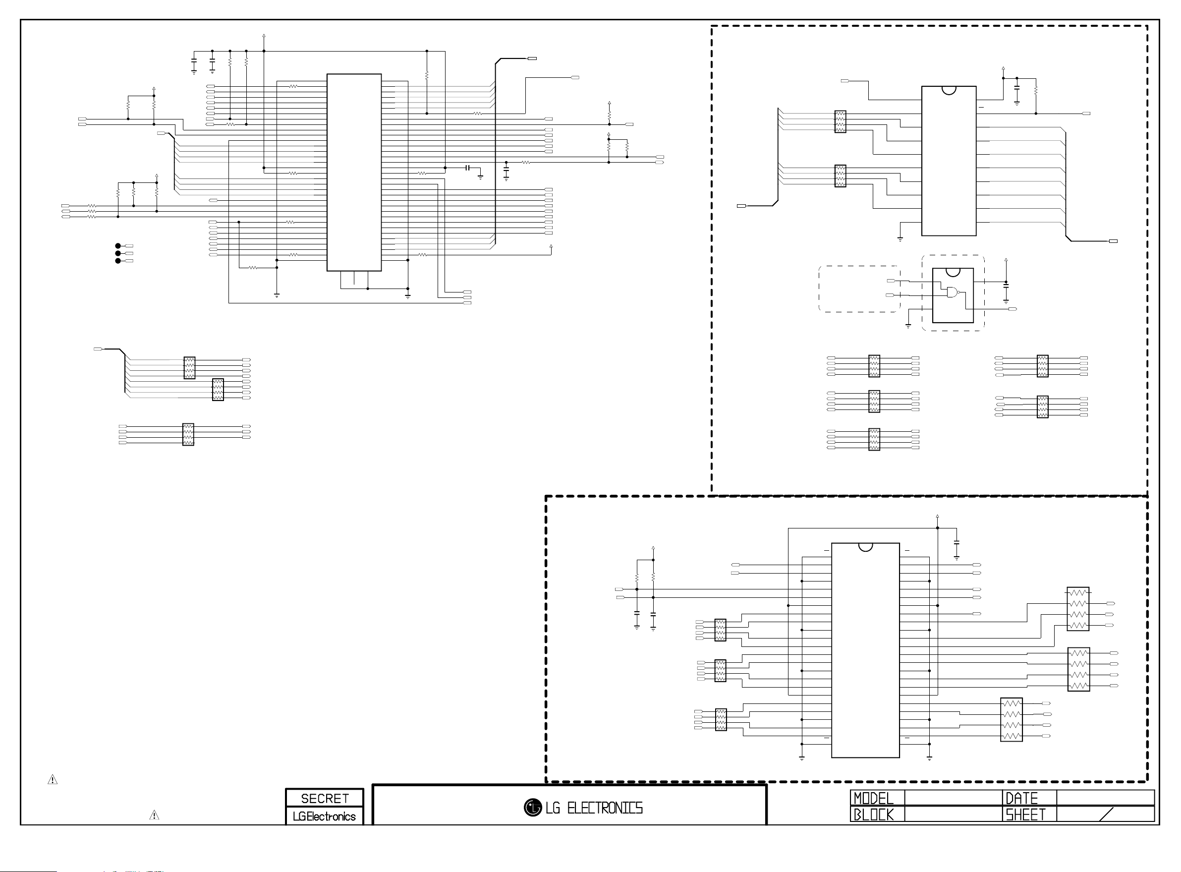
+5V_CI_ON
Copyright ⓒ 2012 LG Electronics. Inc. All right reserved.
Only for training and service purposes
LGE Internal Use Only
CI HOST I/F
PCM_RST
/PCM_WAIT
PCM_INPACK
/PCM_IORD
/PCM_IOWR
R6202
R6203
R6200
CI_IN_TS_DATA[0-7]
R6211
10K
OPT
CI
22
CI
22
OPT
22
+5V_CI_ON
R6204
10K
OPT
R6205
10K
OPT
CI_VS1
PCM_INPACK
/PCM_CE2
R6206
10K
+5V_CI_ON
R6207
10K
OPT
CI
C6200
0.1uF
CI
/CI_CD1
CI_TS_DATA[3]
CI_TS_DATA[4]
CI_TS_DATA[5]
CI_TS_DATA[6]
CI_TS_DATA[7]
/PCM_CE2
CI_VS1
CI_IN_TS_DATA[0]
CI_IN_TS_DATA[1]
CI_IN_TS_DATA[2]
CI_IN_TS_DATA[3]
CI_IN_TS_DATA[4]
CI_IN_TS_DATA[5]
CI_IN_TS_DATA[6]
CI_IN_TS_DATA[7]
CI_TS_CLK
/PCM_REG
CI_TS_VAL
CI_TS_SYNC
CI_TS_DATA[0]
CI_TS_DATA[1]
CI_TS_DATA[2]
/CI_CD2
C6201
10uF
10V
CI
R6249
R6208
10K
OPT
0
OPT
R6210
R6209
10K
OPT
OPT
5V <=> 3.3V
IC904
74LVC245A
DIR
1
A0
2
A1
3
A2
4
A3
5
A4
CI
6
A5
7
A6
8
A7
9
GND
10
IC905
74LVC1G00GW
1B 5 VCC
2A
3GND
CI
AND GATE => NAND GATE
20
19
18
17
16
15
14
13
12
11
4 Y
+3.3V_NORMAL
VCC
OE
B0
B1
B2
B3
B4
B5
B6
B7
CI
+3.3V_NORMAL
CI
C903
0.1uF
16V
C904
0
0.1uF
R913
16V
OPT
EB_DATA[0]
EB_DATA[1]
EB_DATA[2]
EB_DATA[3]
EB_DATA[4]
EB_DATA[5]
EB_DATA[6]
EB_DATA[7]
DIR
/PCM_CE1
EB_DATA[0-7]
EB_DATA[0-7]
CI_ADDR[11]
CI_ADDR[9]
CI_ADDR[13]
R6243 22
C6206
0.1uF
16V
CI_ADDR[12]
CI_ADDR[7]
CI_ADDR[6]
CI_ADDR[5]
CI_ADDR[4]
CI_ADDR[3]
CI_ADDR[2]
CI_ADDR[1]
CI_ADDR[0]
CI_DATA[0-7]
OPT
+5V_CI_ON
CI_ADDR[10]
CI_ADDR[11]
CI_ADDR[9]
CI_ADDR[8]
CI_ADDR[13]
CI_ADDR[14]
CI_ADDR[12]
CI_ADDR[7]
CI_ADDR[6]
CI_ADDR[5]
CI_ADDR[4]
CI_ADDR[3]
CI_ADDR[2]
CI_ADDR[1]
CI_ADDR[0]
/PCM_CE1
+5V_CI_ON
R6245
10K
OPT
+5V_CI_ON
R6244
10K
CI
R6246
10K
/PCM_OE
OPT
/PCM_WE
/PCM_IRQA
CI_DATA[0-7]
CI_DATA[0]
CI_DATA[1]
CI_DATA[2]
CI_DATA[3]
CI_DATA[0-7]
CI_DATA[4]
CI_DATA[5]
CI_DATA[6]
CI_DATA[7]
DIR
CI
AR909
33
CI
AR910
33
WE=>OE
IOWE=>IORD
/PCM_OE
/PCM_IORD
P6200
10067972-000LF CI
GND
/CI_DET1
TS_OUT3
TS_OUT4
TS_OUT5
TS_OUT6
TS_OUT7
CARD_EN2
IORD
IOWR
TS_IN_SYN
TS_IN0
TS_IN1
TS_IN2
TS_IN3
TS_IN4
TS_IN5
TS_IN6
TS_IN7
TS_OUT_CLK
CI_RESET
CI_WAIT
INPACK
TS_OUT_VAL
TS_OUT_SYN
TS_OUT0
TS_OUT1
TS_OUT2
/CI_DET2
35
36
37
38
39
40
41
42
VS1
43
44
45
46
47
48
49
50
VCC
51
VPP
52
53
54
55
56
57
58
59
60
REG
61
62
63
64
65
66
67
GND
68
69
100
R6214
CI
0
R6213
OPT
CI
R6212 0
CI
R6215 100
0
GND
1
DAT3
2
DAT4
3
DAT5
4
DAT6
5
DAT6
6
/CARD_EN1
7
ADDR10
8
/O_EN
9
ADDR11
10
ADDR10
11
ADDR8
12
ADDR13
13
ADDR14
14
/WR_EN
15
/IRQA
16
VCC
17
VPP
18
TS_IN_VAL
19
TS_IN_CLK
20
ADDR12
21
ADDR7
22
ADDR6
23
ADDR5
24
ADDR4
25
ADDR3
26
ADDR2
27
ADDR1
28
ADDR0
29
DAT0
30
DAT1
31
DAT2
32
/IO_BIT
33
GND
34
G1G2
R6216
R6217
R6219
10K
OPT
CI_DATA[3]
CI_DATA[4]
CI_DATA[5]
CI_DATA[6]
CI_DATA[7]
CI
R6224 22
C6205 0.1uF
0
OPT
10K
OPT
CI
CI_DATA[0]
CI_DATA[1]
CI_DATA[2]
CI_IN_TS_VAL
CI_IN_TS_CLK
CI_IN_TS_SYNC
CI_ADDR[10]
CI_ADDR[8]
CI_ADDR[14]
CI
TPO_DATA[0-7]
TPO_CLK
TPO_SOP
TPO_VAL
TPO_ERR
TPO_DATA[0]
TPO_DATA[1]
TPO_DATA[2]
TPO_DATA[3]
TPO_DATA[4]
TPO_DATA[5]
TPO_DATA[6]
TPO_DATA[7]
CI
AR904
33
AR905
CI
AR903
33
CI
33
CI_IN_TS_DATA[0]
CI_IN_TS_DATA[1]
CI_IN_TS_DATA[2]
CI_IN_TS_DATA[3]
CI_IN_TS_DATA[4]
CI_IN_TS_DATA[5]
CI_IN_TS_DATA[6]
CI_IN_TS_DATA[7]
CI_IN_TS_CLK
CI_IN_TS_SYNC
CI_IN_TS_VAL
CI_ADDR[0]
CI_ADDR[1]
CI_ADDR[2]
CI_ADDR[3]
CI_ADDR[4]
CI_ADDR[5]
CI_ADDR[6]
CI_ADDR[7]
CI_ADDR[8]
CI_ADDR[9]
CI_ADDR[10]
CI_ADDR[11]
BUFFER FOR 5V => 3.3V
/CI_CD2
/CI_CD1
+5V_NORMAL
CI
10K
R915
CI
C905
0.1uF
16V
CI
10K
R916
CI
C906
0.1uF
16V
CI_TS_DATA[7]
CI_TS_DATA[6]
CI_TS_DATA[5]
CI_TS_DATA[4]
CI_TS_DATA[3]
CI_TS_DATA[2]
CI_TS_DATA[1]
CI_TS_DATA[0]
PCM_INPACK
CI_TS_CLK
CI_TS_VAL
CI_TS_SYNC
/PCM_WAIT
/PCM_IRQA
AR921
AR920
AR919
CI
100
CI
100
CI
100
GND_8
VCC_4
GND_7
GND_6
VCC_3
GND_5
2OE
48
1A0
47
1A1
46
45
1A2
44
1A3
43
42
2A0
41
2A1
40
39
2A2
38
2A3
37
3A0
36
3A1
35
34
3A2
33
3A3
32
31
4A0
30
4A1
29
28
4A2
27
4A3
26
3OE
25
CI
AR911
33
CI
AR912
33
CI
AR913
33
IC903
74LVC16244ADGG
CI
EB_ADDR[0]
EB_ADDR[1]
EB_ADDR[2]
EB_ADDR[3]
EB_ADDR[4]
EB_ADDR[5]
EB_ADDR[6]
EB_ADDR[7]
EB_ADDR[8]
EB_ADDR[9]
EB_ADDR[10]
EB_ADDR[11]
+3.3V_NORMAL
1OE
1
1Y0
2
1Y1
3
GND_1
4
1Y2
5
1Y3
6
VCC_1
7
2Y0
8
2Y1
9
GND_2
10
2Y2
11
2Y3
12
3Y0
13
3Y1
14
GND_3
15
3Y2
16
3Y4
17
VCC_2
18
4Y0
19
4Y1
20
GND_4
21
4Y2
22
4Y3
23
4OE
24
CI_ADDR[12]
CI_ADDR[13]
CI_ADDR[14]
/PCM_REG
/PCM_OE
/PCM_WE
/PCM_IORD
/PCM_IOWR
C900
0.1uF
16V
CI
CAM_WAIT_N
CAM_IREQ_N
CAM_CD2_N
CAM_CD1_N
CAM_INPACK_N
75
AR916
CI
33
33
AR915
AR914
CI
CI
CI
AR918 75
75
TPI_DATA[3]
TPI_DATA[2]
TPI_DATA[1]
TPI_DATA[0]
EB_ADDR[12]
EB_ADDR[13]
EB_ADDR[14]
CAM_REG_N
EB_OE_N
EB_WE_N
EB_BE_N1
EB_BE_N0
CI
AR917
TPI_CLK
TPI_VAL
TPI_SOP
TPI_DATA[7]
TPI_DATA[6]
TPI_DATA[5]
TPI_DATA[4]
THE SYMBOL MARK OF THIS SCHEMETIC DIAGRAM INCORPORATES
SPECIAL FEATURES IMPORTANT FOR PROTECTION FROM X-RADIATION.
FILRE AND ELECTRICAL SHOCK HAZARDS, WHEN SERVICING IF IS
ESSENTIAL THAT ONLY MANUFATURES SPECFIED PARTS BE USED FOR
THE CRITICAL COMPONENTS IN THE SYMBOL MARK OF THE SCHEMETIC.
Page 24
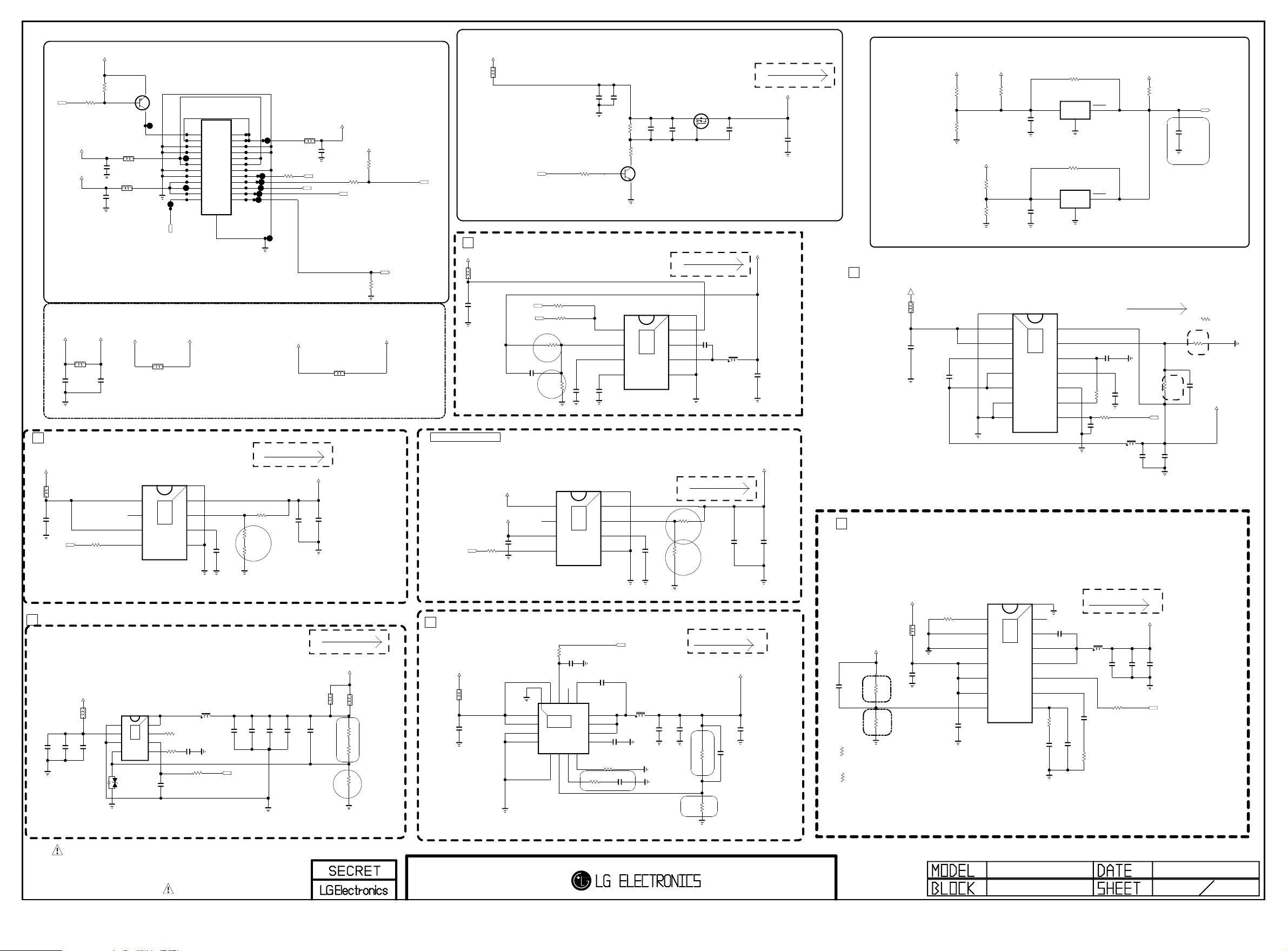
RL_ON
Copyright ⓒ 2012 LG Electronics. Inc. All right reserved.
Only for training and service purposes
LGE Internal Use Only
+3.5V_ST
eMMC POWER
+3.3V_NORMAL
L2319
BLM18PG121SN1D
C2371
0.1uF
16V
1
+3.5V_ST
L2301
BLM18PG121SN1D
C2301
4.7uF
10V
POWER_ON/OFF1
+12V
R2305
10K
C2306
0.1uF
50V
3.3V_EMMC
R2300
10K
+3.5V_ST
10K
1
R2306
2
3
L2303
BLM18SG121TN1D
C2307
0.1uF
16V
CIS21J121
L2302
+1.8V_NORMAL
C2372
0.1uF
16V
+1.8V
AP7173-SPG-13 HF(DIODES)
IN
1
PG
2
VCC
3
EN
4
1.5A
Q2301 MMBT3906(NXP)
GND/P.DIM2
PWM_DIM2
L2306
BLM18PG121SN1D
IC2300
9
THERMAL
PWR ON
24V
GND
GND
3.5V
3.5V
GND
GND
12V
12V
12V
EMMC_VCCQ
[EP]
OUT
8
FB
7
SS
6
GND
5
OPT
P2301
FW20020-24S
LPB
R2302
100
L2305
CIS21J121
C2317
0.1uF
50V
L/DIM0_VS
A_DIM
1
1
3
3
5
5
7
7
9
9
11
11
13
13
15
15
17
17
19
19
21
21 22
23
23 24
25
SMAW200-H24S2
P2300
2
2
4
4
6
6
8
8
10
10
12
12
14
14
16
16
18
18
20
20
22
24
24V
24V
GND
GND
3.5V
3.5V
GND
GND/V-sync
INV ON
A.DIM
P.DIM1
Err OUT
Tuner 1.25V REG Input
+3.3V_TU
293 mA
+1.8V_NORMAL
1%
R1
C2308
2200pF
50V
R2314
3K
1%
R2315
100
1%
1/16W
3.9K
R2321
R2
C2313
10uF
10V
C2315
0.1uF
16V
+24V
R2312
100
PWM_DIM
L2314
BLM18PG121SN1D
+3.3V_NORMAL
R2330
1K
0
R2304
+3.3V_TU_IN
ERROR_OUT
INV_CTL
3. soft start
POWER_ON/OFF2_2
+12V
L2311
CIS21J121
1
+12V
L2310
BLM18PG121SN1D
C2322
10uF
16V
Switching freq: 700K
+3.3V_NORMAL
+5V_NORMAL
R2334
10K
PANEL_POWER
PANEL_CTL
+5V_Normal
R2301
10KPOWER_ON/OFF1
POWER_ON/OFF2_1
R1
C2334
100pF
50V
R2
1%
R2308
R2311
OPT
R2348
10K
56K
10K
1%
+2.5V
AP7173-SPG-13 HF(DIODES)
IN
1
PG
2
VCC
C2324
10uF
10V
3
EN
4
0.01uF
R2341
C2336
1uF
10V
IC2303
THERMAL
1.5A
10K
C2326
50V
9
C2328
0.1uF
50V
C2332
10uF
9
THERMAL
C2335
0.1uF
50V
16V
[EP]GND
VIN
8
VBST
7
SW
6
GND
5
VREG5
C2342
2200pF
50V
VFB
R2343
33K
R2344
5.6K
C
Q2304
B
MMBT3904(NXP)
E
IC2304
TPS54327DDAR
EN
1
2
3
SS
4
3A
Vout=0.765*(1+R1/R2)
[EP]
OUT
8
FB
7
SS
6
GND
5
C2331
2200pF
50V
R2346
2K
1%
R2347
4.3K
1%
AO3407A
OPT
R2
Q2305
R1
S
G
MAX 1A
C2345
0.1uF
16V
D
700 mA
1uF
C2339
OPT
L2313
6.8uH
NR8040T4R7N
C2340
10uF
10V
25V
+2.5V_NORMAL
TYP 1450mA
+5V_NORMAL
C2343
22uF
10V
C2344
0.1uF
16V
PANEL_VCC
C2346
0.1uF
50V
Power_DET
+12V
4
+12V
L2309
BLM18PG121SN1D
C2354
10uF
16V
C2303
0.1uF
50V
4
+3.5V_ST
+24V
PD_24V
R2364
8.2K
1%
PD_24V
R2365
1.5K
1%
PD_+3.5V
R2366
0
5%
C2359
0.1uF
16V
C2360
0.1uF
16V
VCC
VCC
PD_24V
PD_+12V
R2362
2.7K
1%
PD_+12V
R2363
1.2K
1%
+1.0V_VDD
VIN2
VIN1
VBST
SW2
SW1
IC2306
TPS54425PWPR
14
13
12
4A
11
10
9
8
THERMAL
15
1
2
3
4
5
6
7
[EP]PGND
PGND2
PGND1
Vout=0.765*(1+R1/R2)
R2373
100K
IC2307
NCP803SN293
3
1
GND
PD_24V
R2372
100K
PD_24V
IC2308
NCP803SN293
3
1
GND
VO
VFB
VREG5
SS
GND
PG
EN
RESET
2
RESET
2
R2309
100K
R2310 10K
C2305
0.1uF
OPT
C2318
1uF
10V
+3.5V_ST
R2376
10K
OPT
not to RESET at 8kV ESD
LG1152 Max: 1728 mA
LG1132 Max: 2000 mA
R1
R2313
9.1K
C2368
22uF
10V
1%
C2369
22uF
10V
C2319
3300pF
50V
POWER_ON/OFF2_3
L2316
2uH
POWER_DET
C2365
0.1uF
16V
24V-->3.48V
12V-->3.58V
ST_3.5V-->3.5V
URSA5
R2322-*1
24K
1%
R2
R2322
22K
1%
FRC3
OPT
C2321
22pF
50V
+1.0VDC
Vout=0.8*(1+R1/R2)
2
C2353
3300pF
50V
OPT
MAX 4.7 A
+3.3V_NORMAL
OPT
L2318
CIS21J121
R2319
R2382
30K
R2320
10K
L2307
CIS21J121
R1
1%
1.5K
1/16W
1%
1%
R2
L2300
BLM18PG121SN1D
Placed on SMD-TOP
C2300
C2304
10uF
10uF
16V
16V
+12V
+3.3V_NORMAL
IC2301
[EP]LX
AOZ1038PI
C2309
0.1uF
16V
OPT
PGND
VIN
AGND
FB
NC_2
1
8
NC_1
9
2
7
THERMAL
EN
3
6
COMP
4
5
6A
D2350
ADUC 20S 02 010L
*NOTE 17
OPT
R23160
R2317
20K
C2310
0.1uF
16V
C2311
2200pF
50V
R2318
L2304
2uH
10K
C2312
10uF
10V
POWER_ON/OFF2_1
C2314
10uF
10V
C2316
10uF
10V
C2352
10uF
10V
Vout=0.8*(1+R1/R2)
THE SYMBOL MARK OF THIS SCHEMETIC DIAGRAM INCORPORATES
SPECIAL FEATURES IMPORTANT FOR PROTECTION FROM X-RADIATION.
FILRE AND ELECTRICAL SHOCK HAZARDS, WHEN SERVICING IF IS
ESSENTIAL THAT ONLY MANUFATURES SPECFIED PARTS BE USED FOR
THE CRITICAL COMPONENTS IN THE SYMBOL MARK OF THE SCHEMETIC.
C2302
4.7uF
16V
RT/CLK
GND_1
GND_2
PVIN_1
PVIN_2
VIN
VSENSE
IC2305
EAN62348501
1
15
2
THERMAL
3
4
5
6
7
[EP]GND
PWRGD
14
C2349
BOOT
13
0.1uF
16V
PH_2
12
PH_1
11
EN
10
SS/TR
9
COMP
8
1.3K
R2307
C2348
4700pF 50V
47pF 50V
22000pF 50V
C2373
R2381 0
Max 5926 mA
L2317
1uH
R2357 1K
C2374
1/16W
5%
Switching freq: 400 ~ 580 Khz
+0.9V_VDD
C2363
C2350
22uF
22uF
10V
10V
POWER_ON/OFF2_3
OPT
C2370
10uF
10V
Vout=0.8*(1+R1/R2)
4
+3.5V_ST
DDR MAIN 1.5V
L2308
C2320
10uF
10V
VIN_1
VIN_2
GND_1
GND_2
EP[GND]
1
2
3
4
10K
R2339
C2325
THERMAL
17
IC2302
TPS54319TRE
3A
5
6
COMP
AGND
VSENSE
3A
0.1uF
16V
7
BOOT14PWRGD15EN16VIN_3
13
12
11
10
9
8
RT/CLK
1/16W 5%
$ 0.145
PH_3
PH_2
PH_1
SS/TR
R2340
15K
C2327
0.1uF
16V
R2342
C2329
0.01uF
50V
330K1/16W 5%
C2330
4700pF
50V
NR8040T3R6N
POWER_ON/OFF2_3
L2312
3.6uH
C2333
22uF
10V
C2337
22uF
10V
1074 mA
+1.5V_DDR
C2341
0.1uF
16V
C2338
100pF
50V
R2349
R1
47K 1%
R2
R2350
56K
1/16W
1%
C2375
180pF
50V
R2378-*1
8.2K
1/16W
R2379-*1
15K
+0.9V_VDD
R2378
6.8K
R2379
12K
URSA5
1%
URSA5
1/16W
1%
Vout=0.6*(1+R1/R2)
1/16W
1/16W
+12V
R2377
100K
C2347
10uF
16V
1/16W
5%
L2315
R1
1%
FRC3
R2
1%
FRC3
Vout=0.827*(1+R1/R2)=1.521V
LG1152
POWER
Page 25
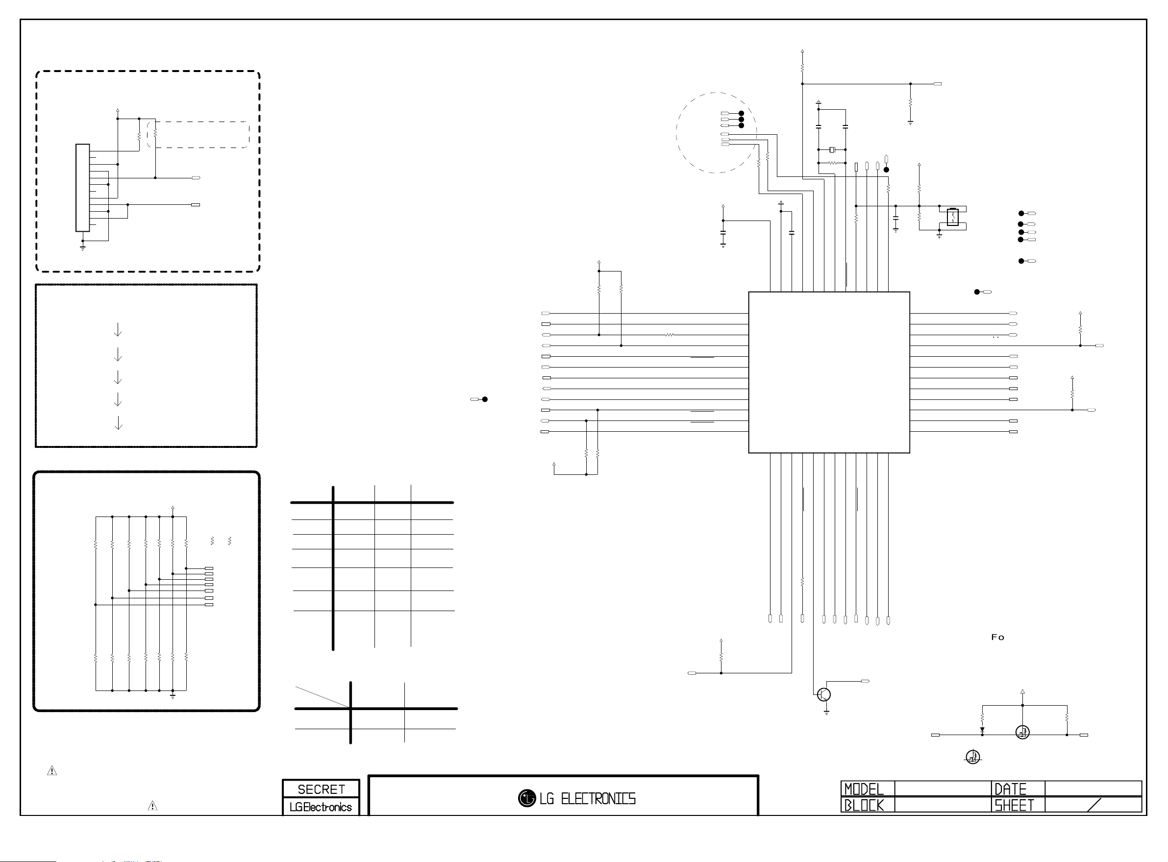
Renesas MICOM
Copyright ⓒ 2012 LG Electronics. Inc. All right reserved.
Only for training and service purposes
LGE Internal Use Only
For Debug
+3.5V_ST
MICOM_DEBUG
P3000
12507WS-12L
1
2
3
4
5
6
7
8
9
10
11
12
13
GP4 High/MID Power SEQUENCE
POWER_ON/OFF!
POWER_ON/OFF2_1
POWER_ON/OFF2_2
POWER_ON/OFF2_3
POWER_ON/OFF2_4
SOC_RESET
MICOM MODEL OPTION
MICOM_MHL
MICOM_GED
R3016 10K
R3020 10K
MICOM_GP4_10PIN
R3030 10K
Don’t remove R3014,
Not making P40 floated
R3014 1K
R3011 10K
MICOM_DEBUG
+3.5V_ST
MICOM_PDP
R3007 10K
R3005 10K
MICOM_JAPAN
MICOM_TOUCH_KEY
R3009 10K
MICOM_DEBUG
MICOM_RESET
R3005-*1
R3012 10K
MICOM_OLED_MAIN
MICOM_LOGO_LIGHT
R3005-*2
56K
MICOM_OLED_FRC
MODEL1_OPT_0
MODEL1_OPT_1
MODEL1_OPT_2
MODEL1_OPT_3
MODEL1_OPT_4
MODEL1_OPT_5
MODEL1_OPT_6
+3.3V_NORMAL
R3035
4.7K
MICOM MODEL OPTION
POWER_ON/OFF2_3
I2C_SCL3
I2C_SDA3
AMP_RESET_N
PANEL_CTL
MODEL1_OPT_5
HDMI_CEC
POWER_ON/OFF2_2
POWER_ON/OFF2_3
EEPROM_SDA
EEPROM_SCL
MODEL1_OPT_6
AMP_RESET_BY_MICOM
IR
+3.5V_ST
R3018
3.3K
+3.3V_NORMAL
R3032
10K
R3033
10K
R3003 22
AMP_RESET_BY_MICOM
P31/TI03/TO03/INTP4
P75/KR5/INTP9/SCK01/SCL01
P74/KR4/INTP8/SI01/SDA01
P71/KR1/SI21/SDA21
P70/KR0/SCK21/SCL21
P30/INTP3/RTC1HZ/SCK11/SCL11
R3019
3.3K
FLG_POD_DR
POD_WAKEUP_N
/RST_DIIVA
/RST_DIIVA
POD_WAKEUP_N
FLG_POD_DR
for DiiVA
+3.5V_ST
C3000
0.1uF
P60/SCLA0
P61/SDAA0
P62
P63
P73/KR3/SO01
P72/KR2/SO21
R3002 22
MICOM_DIIVA
R3001 22
MICOM_DIIVA
VDD
48
1
2
3
4
5
6
7
8
9
10
11
12
13
GND
VSS
47
14
C3001 0.47uF
REGC
46
15
OPT
8pF
C3002
C3003 8pF
X3000
32.768KHz
R3023
4.7M
OPT
P124/XT2/EXCLKS
P123/XT1
P137/INTP0
P122/X2/EXCLK
P121/X1
41
42
43
44
45
IC3000
R5F100GEAFB
MICOM
16
17
18
19
20
MICOM_DEBUG
LOGO_LIGHT
MICOM_RESET
MICOM_DIIVA
R3024 22
P41/TI07/TO07
P40/TOOL0
RESET
38
39
40
21
22
23
P146
10K
R3000
LOGO_LIGHT
+3.5V_ST
R3025 22
C3004
0.1uF
16V
P120/ANI19
37
36
35
34
33
32
31
30
29
28
27
26
25
24
12V_EXT_PWR_DET
HDMI_WAUP:HDMI_INIT
10K
MICOM_RESET_SW
SW3000
R3026
JTP-1127WEM
12
4 3
R3027
270K
OPT
P140/PCLBUZ0/INTP6
P00/TI00/TXD1
P01/TO00/RXD1
For Japan:LNB_INIT
P130
P20/ANI0/AVREFP
P21/ANI1/AVREFM
P22/ANI2
P23/ANI3
P24/ANI4
P25/ANI5
P26/ANI6
P27/ANI7
POWER_ON/OFF2_4
RL_ON
SCART_MUTE
POWER_ON/OFF2_4
KEY2
KEY1
MODEL1_OPT_2
MODEL1_OPT_1
MODEL1_OPT_0
MODEL1_OPT_4
MODEL1_OPT_3
EXT_AMP_MUTE
EXT_AMP_RESET
COMMERCIAL_12V_CTL
12V_EXT_PWR_DET
SCART_MUTE
+3.3V_NORMAL
+3.3V_NORMAL
R3036
10K
OPT
R3037
10K
OPT
POWER_ON/OFF2_1
SIDE_HP_MUTE
10
P147/ANI18
P10/SCK00/SCL00
/ OLED
LOGO_LIGHT
JAPAN
TOUCH_KEY
PDP
IR Wafer
10Pin
(GP4_TOOL)
MHLMODEL_OPT_5
GEDMODEL_OPT_6
For LM86
For JAPAN
For Sample Set
GP4_HIGH
P17/TI02/TO02
P51/INTP2/SO11
P50/INTP1/SI11/SDA11
P16/TI01/TO01/INTP5
P13/TXD2/SO20
P14/RXD2/SI20/SDA20
P12/SO00/TXD0/TOOLTXD
P15/PCLBUZ1/SCK20/SCL20
P11/SI00/RXD0/TOOLRXD/SDA00
R30 22 10 K
MODEL_OPT_0
MODEL_OPT_1
22K
MODEL_OPT_2
MODEL_OPT_3
MODEL_OPT_4
NON LOGO_LIGHT
NON JAPAN
TACT_KEY
LCD
IR Wafer
12/15Pin
(GP3_Soft touch)
NON_MHL
NON_GED
R3006 10K
R3008 10K
R3010 10K
R3021 10K
R3017 10K
MICOM_NON_MHL
MICOM_NON_GED
R3031 10K
MICOM_LCD/OLED
MICOM_GP3_12/15PIN
MICOM_TACT_KEY
R3013 10K
MICOM_NON_JAPAN
MICOM_NON_LOGO_LIGHT
THE SYMBOL MARK OF THIS SCHEMETIC DIAGRAM INCORPORATES
SPECIAL FEATURES IMPORTANT FOR PROTECTION FROM X-RADIATION.
FILRE AND ELECTRICAL SHOCK HAZARDS, WHEN SERVICING IF IS
ESSENTIAL THAT ONLY MANUFATURES SPECFIED PARTS BE USED FOR
THE CRITICAL COMPONENTS IN THE SYMBOL MARK OF THE SCHEMETIC.
Eye Sensor Option
MODEL_OPT_4
MODEL_OPT_2
0
1
0
N/A
CM3231_CAPELLA
(GP3 Soft touch) (GP4 Soft touch)
1
MC8101_ABOV
(TACT_KEY)
CM3231_CAPELLA
POWER_ON/OFF1
+3.3V_NORMAL
R3034
4.7K
POWER_DET
OPT
COMMERCIAL_12V_CTL
LED_B/GP4_LED_R
B
SOC_RESET
C
Q3000
MMBT3904(NXP)
EDID_WP
E
SOC_TX
AMP_MUTE
EDID_WP
EXT_AMP_RESET
EXT_AMP_MUTE
CEC_REMOTE
BAT54_SUZHO
SOC_RX
INV_CTL
D3000
D
G
S
For CEC
+3.5V_ST
R3028
27K
Q3001-*1
SI1012CR-T1-GE3
HDMI_CEC_FET_VISHAY
G
D
S
Q3001
RUE003N02
HDMI_CEC_FET_ROHM
R3029
120K
HDMI_CEC
2011.12.12
MICOM
30
Page 26
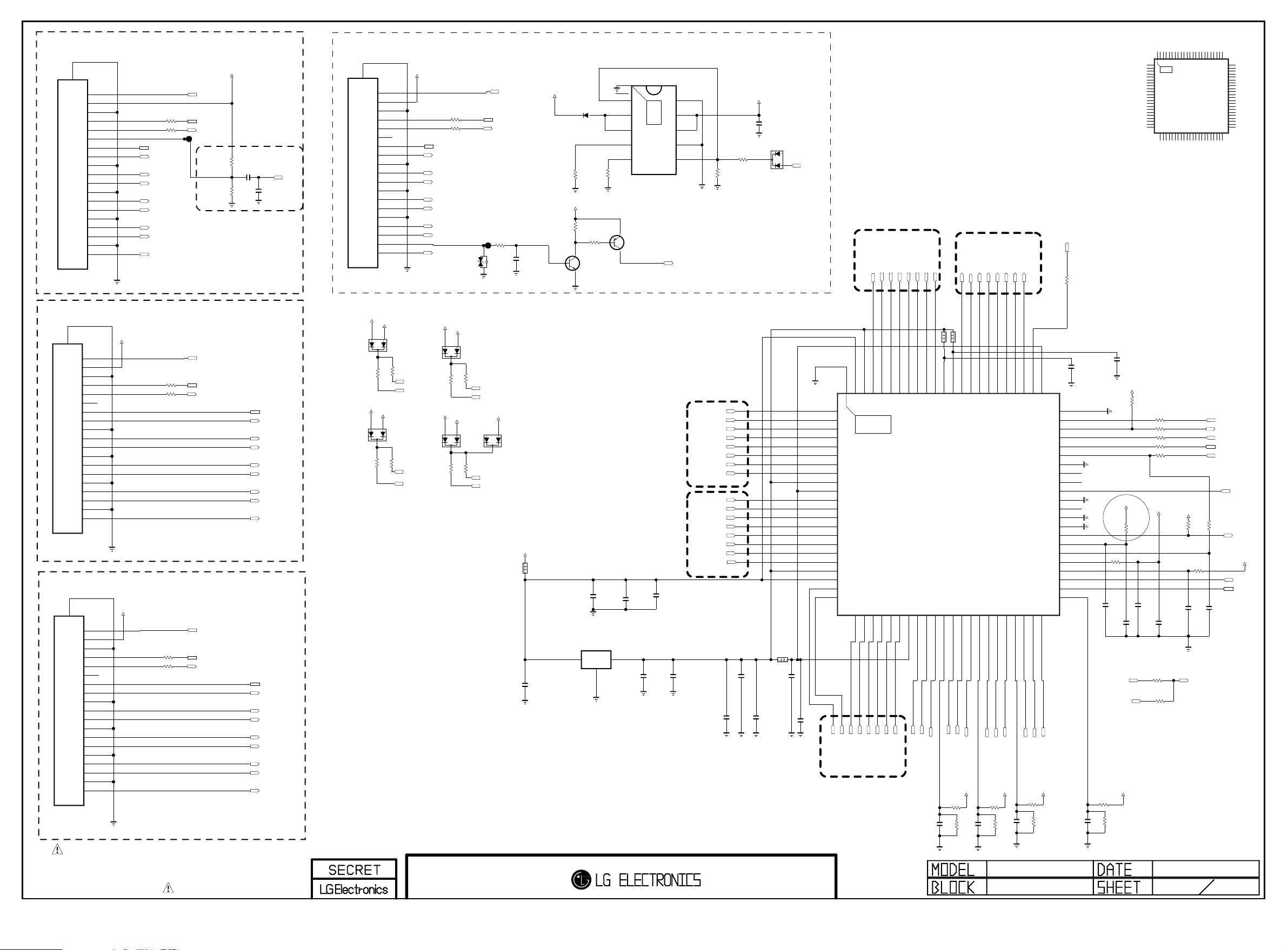
BODY_SHIELD
Copyright ⓒ 2012 LG Electronics. Inc. All right reserved.
Only for training and service purposes
LGE Internal Use Only
20
EAG62611201
JK3202
RSD-105156-100
BODY_SHIELD
20
19
18
17
16
15
14
13
12
11
10
EAG62611201
JK3200
RSD-105156-100
BODY_SHIELD
20
19
18
17
16
15
14
13
12
11
10
EAG62611201
JK3201
RSD-105156-100
19
18
17
16
15
14
13
12
11
10
9
8
7
6
5
4
3
2
1
9
8
7
6
5
4
3
2
1
9
8
7
6
5
4
3
2
1
HP_DET
5V
GND
DDC_DATA
DDC_CLK
ARC
CE_REMOTE
CK-
CK_GND
CK+
D0-
D0_GND
D0+
D1-
D1_GND
D1+
D2-
D2_GND
D2+
HP_DET
5V
GND
DDC_DATA
DDC_CLK
NC
CE_REMOTE
CK-
CK_GND
CK+
D0-
D0_GND
D0+
D1-
D1_GND
D1+
D2-
D2_GND
D2+
HP_DET
5V
GND
DDC_DATA
DDC_CLK
NC
CE_REMOTE
CK-
CK_GND
CK+
D0-
D0_GND
D0+
D1-
D1_GND
D1+
D2-
D2_GND
D2+
5V_HDMI_2
5V_HDMI_3
HDMI_HPD_1
R3207 0
R3208 0
CEC_REMOTE
CK-_HDMI1
CK+_HDMI1
D0-_HDMI1
D0+_HDMI1
D1-_HDMI1
D1+_HDMI1
D2-_HDMI1
D2+_HDMI1
DDC_SDA_1
DDC_SCL_1
HDMI1 With ARC
HDMI_HPD_2
R3209
0
R3210
0
R3204
0
R3205
0
DDC_SDA_2
DDC_SCL_2
HDMI_HPD_3
DDC_SDA_3
DDC_SCL_3
5V_HDMI_1
R3248
1K
OPT
R3249
3.9K
OPT
HDMI2
C3202
1uF
10V
HDMI3
SPDIF_OUT_ARC
OPT
C3226
0.1uF
16V
CEC_REMOTE
CK-_HDMI2
CK+_HDMI2
D0-_HDMI2
D0+_HDMI2
D1-_HDMI2
D1+_HDMI2
D2-_HDMI2
D2+_HDMI2
CEC_REMOTE
CK-_HDMI3
CK+_HDMI3
D0-_HDMI3
D0+_HDMI3
D1-_HDMI3
D1+_HDMI3
D2-_HDMI3
D2+_HDMI3
ARC
BODY_SHIELD
GND
20
19
18
17
16
15
14
13
12
11
10
9
8
EAG62611201
7
6
5
4
3
2
1
RSD-105156-100
JK3203
+5V_NORMAL
D3200
R3217
47K
+5V_NORMAL
D3201
R3218
47K
HP_DET
5V
GND
DDC_DATA
DDC_CLK
NC
CE_REMOTE
CK-
CK_GND
CK+
D0-
D0_GND
D0+
D1-
D1_GND
D1+
D2-
D2_GND
D2+
5V_HDMI_1
A2CA1
5V_HDMI_3
A2CA1
R3219
47K
R3220
47K
DDC_SDA_3
DDC_SCL_3
5V_HDMI_4
DDC_SDA_1
DDC_SCL_1
CEC_REMOTE
CK-_HDMI4
CK+_HDMI4
D0-_HDMI4
D0+_HDMI4
D1-_HDMI4
D1+_HDMI4
D2-_HDMI4
D2+_HDMI4
+5V_NORMAL
D3202
R3225
47K
+5V_NORMAL
D3203
R3226
47K
R3222
0
R3223
0
5V_HDMI_2
5V_HDMI_4
33
34
36
37
38
40
41
42
DSDA135DSCL1
DSDA339DSCL3
DSDA443DSCL4
R0PWR5V
R1PWR5V
R3PWR5V
CBUS_HPD1
CBUS_HPD3
HDMI_INT
I2C_SCL5
I2C_SDA5
10K
10K
R3203
R3242
10
C3221
C3222
1uF
10uF
10V
10V
12V_EXT_PWR_DET
VDD12_368ARC69TX2P70TX2N71TX1P72TX1N73TX0P74TX0N75TXCP76TXCN77TCVDD1278TPVDD1279R0XCN80R0XCP81R0X0N82R0X0P83R0X1N84R0X1P85R0X2N86R0X2P87AVDD12_388VDD33_2
67
RSVDL
66
SPDIF_IN
65
INT
64
CSCL
63
CSDA
62
RESET_N
61
TPWR
60
GPIO1
59
GPIO0
58
CD-SENSE4
57
CD_SENSE3
56
GPIO2
55
CD_SENSE1
54
CD_SENSE0
53
WKUP
52
LPSBV
51
PWRMUX_OUT
50
SBVCC5
49
R5PWR5V[VGA]
48
DSCL5[VGA]
47
DSDA5[VGA]
46
R4PWR5V
45
44
CBUS_HPD4
SPDIF_OUT
HDMI_S/W_RESET
MHL_DET
R3244
HDMI_WKUP
RGB_5V
RGB_DDC_SCL
RGB_DDC_SDA
[EP]GND
UD
R1XCN
1
R1XCP
2
THERMAL
R1X0N
3
89
R1X0P
4
R1X1N
1/16W
R3213
5.1K
5%
C3212
1uF
10V
R1X1P
R1X2N
R1X2P
AVDD12_1
VDD12_1
R3XCN
R3XCP
R3X0N
R3X0P
R3X1N
R3X1P
R3X2N
R3X2P
AVDD12_2
VDD33_1
R4XCN
R4XCP
10K
R3202
R3224 33
R3211 33
R3236 33
R3237 33
R3214 33
+5V_NORMAL
C3215
0.1uF
16V
OPT
R3215 33
R3212 33
5
6
7
8
9
10
11
12
13
14
15
16
17
18
19
20
21
22
23
R4X0N24R4X0P25R4X1N26R4X1P27R4X2N28R4X2P
OPT
C3218
10uF
10V
IC3201-*1
SII9587CNUC-3
29
30
32
DSDA031DSCL0
VDD12_2
CBUS_HPD0
+3.3V_NORMAL
IC3202
[EP]
HDMI_HPD_4
DDC_SDA_4
DDC_SCL_4
R3243
1K
1/16W
5%
5.6V
D3207
A2CA1
R3228
47K
DDC_SDA_2
DDC_SCL_2
+3.5V_ST
A2CA1
D3205
R3229
47K
DDC_SDA_4
DDC_SCL_4
A2CA1
+3.3V_NORMAL
C3200
10uF
10V
C3223
0.047uF
25V
Q3200
MMBT3904(NXP)
L3200
BLM18PG121SN1D
5V_HDMI_4
MBR230LSFT1G
Limit 0.8A
+3.5V_ST
R3246
B
D3206
30V
1/10W
R3200
62K
1/10W
OPT
Limit 0.8A
10K
R3247
10K
B
C
E
C3205
10uF
10V
IC3200
AZ1117BH-1.2TRE1
IN
2
3
1
GND/ADJ
TPS2554
FAULT
OUT_2
OUT_1
ILIM0
ILIM1
R3201
62K
E
MMBT3906(NXP)
C
10
9
8
7
6
Q3201
THERMAL
11
1
2
3
4
5
MHL_DET
GND
IN_1
IN_2
ILIM_SEL
EN
HDMI2
HDMI3
C3211
C3210
0.1uF
0.1uF
16V
16V
OUT
C3201
C3203
10uF
10uF
10V
10V
Vout=0.8*(1+R1/R2)
+5V_NORMAL
C3208
0.1uF
5%
5%
1/16W
220K
1/16W
R3245
R3206
C
10K
HDMI4 With MHL
CK-_HDMI2
CK+_HDMI2
D0-_HDMI2
D0+_HDMI2
D1-_HDMI2
D1+_HDMI2
D2-_HDMI2
D2+_HDMI2
CK-_HDMI3
CK+_HDMI3
D0-_HDMI3
D0+_HDMI3
D1-_HDMI3
D1+_HDMI3
D2-_HDMI3
D2+_HDMI3
C3206
0.1uF
16V
C3204
C3207
0.1uF
0.1uF
16V
16V
D3204
A1
A2
L3201
BLM18PG121SN1D
C3216
10uF
10V
MHL_DET
R1XCN
R1XCP
R1X0N
R1X0P
R1X1N
R1X1P
R1X2N
R1X2P
AVDD12_1
VDD12_1
R3XCN
R3XCP
R3X0N
R3X0P
R3X1N
R3X1P
R3X2N
R3X2P
AVDD12_2
VDD33_1
R4XCN
R4XCP
C3217
0.1uF
16V
HDMI1
D1-_HDMI1
D0-_HDMI1
D0+_HDMI1
D1+_HDMI1
D2-_HDMI1
D2+_HDMI1
R0X0N
R0X0P
R0X1N
R0X1P
R0X2N
R0X2P
AVDD12_3
VDD33_2
[EP]GND
81
82
83
84
85
86
87
88
1
2
THERMAL
3
89
4
5
6
7
8
9
10
SII9587CNUC
11
12
13
14
Device Address : 0XB0
15
16
17
18
19
20
21
22
23
R4X0N24R4X0P25R4X1N26R4X1P27R4X2N28R4X2P
D1-_HDMI4
D0+_HDMI4
D0-_HDMI4
CK+_HDMI4
CK-_HDMI4
D2-_HDMI4
D1+_HDMI4
HDMI4
29
VDD12_2
D2+_HDMI4
30
DSDA031DSCL0
DDC_SDA_1
CK-_HDMI1
CK+_HDMI1
L3202
TPVDD12
R0XCN
R0XCP
79
80
IC3201
FHD
32
R0PWR5V
CBUS_HPD0
DDC_SCL_1
HDMI_HPD_1
C3213
L3203
TCVDD12
77
78
33
34
DSDA135DSCL1
DDC_SDA_2
5V_HDMI_1
R3231
10
1uF
HDMI_CLK-
TXCN
76
DDC_SCL_2
1/16W
R3233
5.1K
5%
HDMI S/W OUTPUT
HDMI_RX1-
HDMI_RX0-
HDMI_RX0+
TX1N
TX0P
TX0N
73
74
37
38
DSDA339DSCL3
R1PWR5V
DDC_SDA_3
5V_HDMI_2
R3232
10
C3214
1uF
HDMI_RX1+
TX1P
71
72
40
CBUS_HPD3
DDC_SCL_3
HDMI_HPD_3
1/16W
R3234
5.1K
5%
HDMI_CLK+
TXCP
75
36
CBUS_HPD1
HDMI_HPD_2
HDMI_RX2-
HDMI_RX2+
ARC69TX2P
TX2N
70
41
42
DSDA443DSCL4
R3PWR5V
DDC_SDA_4
5V_HDMI_3
R3240
10
C3220
1uF
VDD12_3
67
68
66
65
64
63
62
61
60
59
58
57
56
55
54
53
52
51
50
49
48
47
46
45
44
CBUS_HPD4
DDC_SCL_4
HDMI_HPD_4
1/16W
R3241
5.1K
5%
SPDIF_OUT_ARC
R3221
10
OPT
C3224
0.1uF
16V
RSVDL
SPDIF_IN
INT
CSCL
CSDA
RESET_N
TPWR
GPIO1
GPIO0
CD-SENSE4
CD_SENSE3
GPIO2
CD_SENSE1
CD_SENSE0
WKUP
LPSBV
PWRMUX_OUT
SBVCC5
R5PWR5V[VGA]
DSCL5[VGA]
DSDA5[VGA]
R4PWR5V
C3219
1uF
16V
0.1uF
C3225
HDMI_WKUP
5V_HDMI_4
R3238
10
+3.3V_NORMAL
+3.5V_ST
R3216
10
C3209
0.1uF
16V
MHL_DET
1/16W
R3239
5.1K
5%
THE SYMBOL MARK OF THIS SCHEMETIC DIAGRAM INCORPORATES
SPECIAL FEATURES IMPORTANT FOR PROTECTION FROM X-RADIATION.
FILRE AND ELECTRICAL SHOCK HAZARDS, WHEN SERVICING IF IS
ESSENTIAL THAT ONLY MANUFATURES SPECFIED PARTS BE USED FOR
THE CRITICAL COMPONENTS IN THE SYMBOL MARK OF THE SCHEMETIC.
GP4
2011.10.19
HDMI 32
Page 27
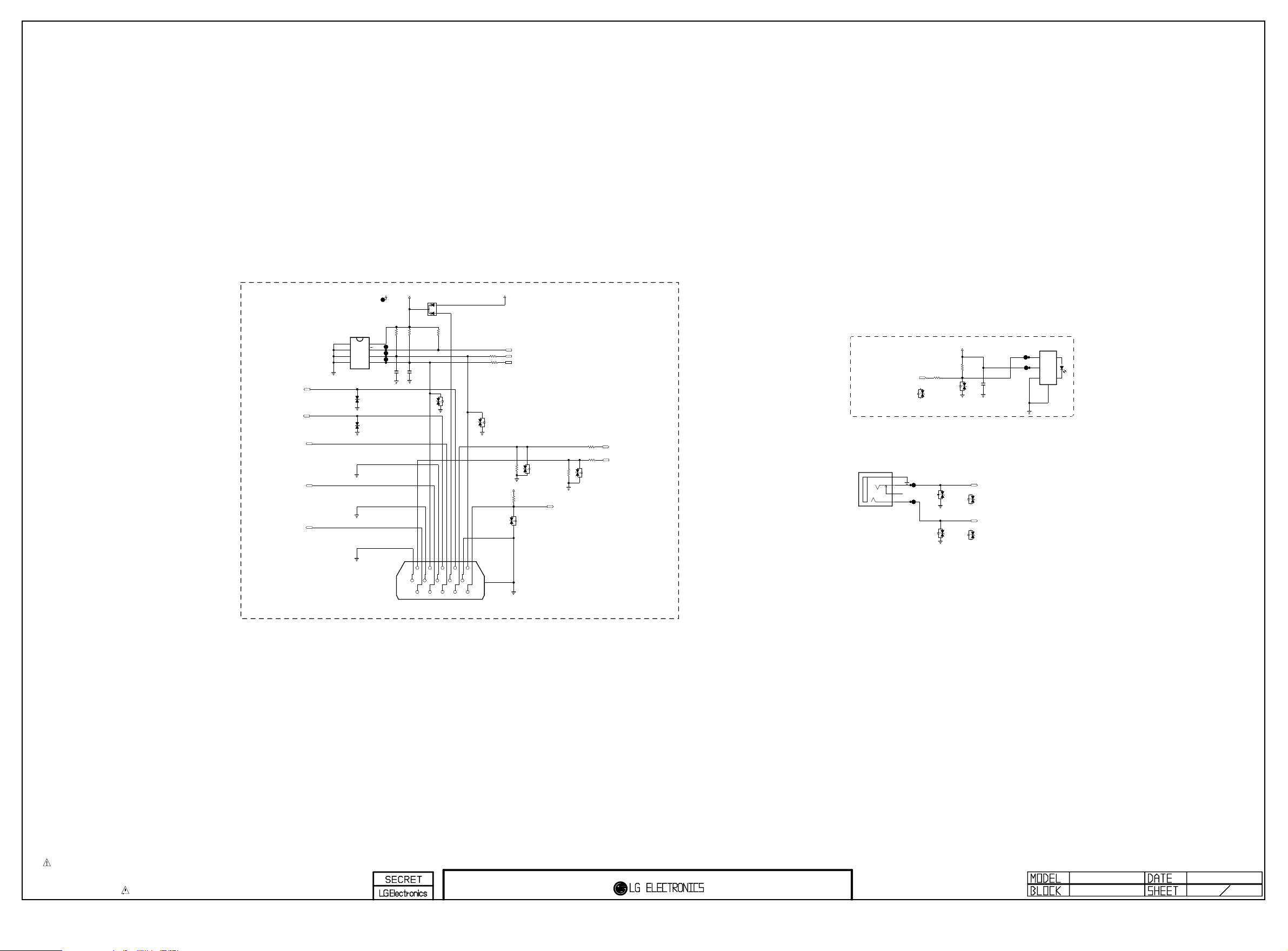
RGB/ PC AUDIO/ SPDIF
Copyright ⓒ 2012 LG Electronics. Inc. All right reserved.
Only for training and service purposes
LGE Internal Use Only
RGB PC
DSUB_VSYNC
DSUB_HSYNC
DSUB_R+
DSUB_B+
DSUB_G+
M24C02-RMN6T
E0
E1
E2
VSS
1
RGB_EDID
2
3
4
IC3600
D3615
30V
OPT
D3616
30V
OPT
RGB_5V
VCC
8
WC
7
SCL
6
SDA
5
Closed to JACK
C3633
18pF
RGB_5V
R3641
2.7K
C3634
18pF
50V
50V
A1
C
A2
MMBD6100
D3620
R3645
R3642
10K
2.7K
RGB_EDID
D3621
ADUC 5S 02 0R5L
5.5V
OPT
91010
111112121313141415
6677889
112233445
JK3603
SLIM-15F-D-2
+5V_NORMAL
JK3602
2F11TC1-EM52-4F
VIN
A
VCC
B
GND
C
Fiber Optic
4
SHIELD
R3620
2.7K
R3615
33
D3613
5.5V
ADUC 5S 02 0R5L
D3612-*1
OPT
OPT
D3611-*1
ESD_MTK
ESD_MTK
5.6V
+3.3V_NORMAL
5.6V
PC_L_IN
PC_R_IN
C3615
0.1uF
16V
EDID_WP
R3643 22
RGB_DDC_SCL
R3644 22
RGB_DDC_SDA
D3622
ADUC 5S 02 0R5L
5.5V
OPT
RGB_DEBUG
R3602
100
SOC_RX
RGB_DEBUG
R3647
100
R3600
D3600
0
20V
R3601
+3.3V_NORMAL
R3646
10K
D3623
5.6V
OPT
OPT
NON_RGB_DEBUG
DSUB_DET
0
NON_RGB_DEBUG
5
15
16
16
D3601
SOC_TX
20V
OPT
SPDIF OUT
PC AUDIO
JK3601
KJA-PH-0-0177
SPDIF_OUT
D3613-*1
5.5V
ADUC 5S 02 0R5L
ESD_MTK
5 GND
4 L
3 DETECT
1 R
D3612
5.6V
OPT
D3611
5.6V
OPT
THE SYMBOL MARK OF THIS SCHEMETIC DIAGRAM INCORPORATES
SPECIAL FEATURES IMPORTANT FOR PROTECTION FROM X-RADIATION.
FILRE AND ELECTRICAL SHOCK HAZARDS, WHEN SERVICING IF IS
ESSENTIAL THAT ONLY MANUFATURES SPECFIED PARTS BE USED FOR
THE CRITICAL COMPONENTS IN THE SYMBOL MARK OF THE SCHEMETIC.
JACK HIGH / MID
2011.11.21
36
Page 28
HP_LOUT
Copyright ⓒ 2012 LG Electronics. Inc. All right reserved.
Only for training and service purposes
LGE Internal Use Only
HP_ROUT
HP_DET
+3.3V_NORMAL
R3700
10K
HP_OUT
VA3700
5.6V
OPT
JK3700
KJA-PH-0-0177
5GND
4L
3DETECT
1R
EAG61030001
HP_OUT
THE SYMBOL MARK OF THIS SCHEMETIC DIAGRAM INCORPORATES
SPECIAL FEATURES IMPORTANT FOR PROTECTION FROM X-RADIATION.
FILRE AND ELECTRICAL SHOCK HAZARDS, WHEN SERVICING IF IS
ESSENTIAL THAT ONLY MANUFATURES SPECFIED PARTS BE USED FOR
THE CRITICAL COMPONENTS IN THE SYMBOL MARK OF THE SCHEMETIC.
ESD for MTK
VA3700-*1
5.6V
ESD_MTK_HP_OUT
ESD for LG1152
VA3700-*2
5.6V
ESD_LG1152_HP_OUT
JACK_COMMON
2011.11.21
37
Page 29
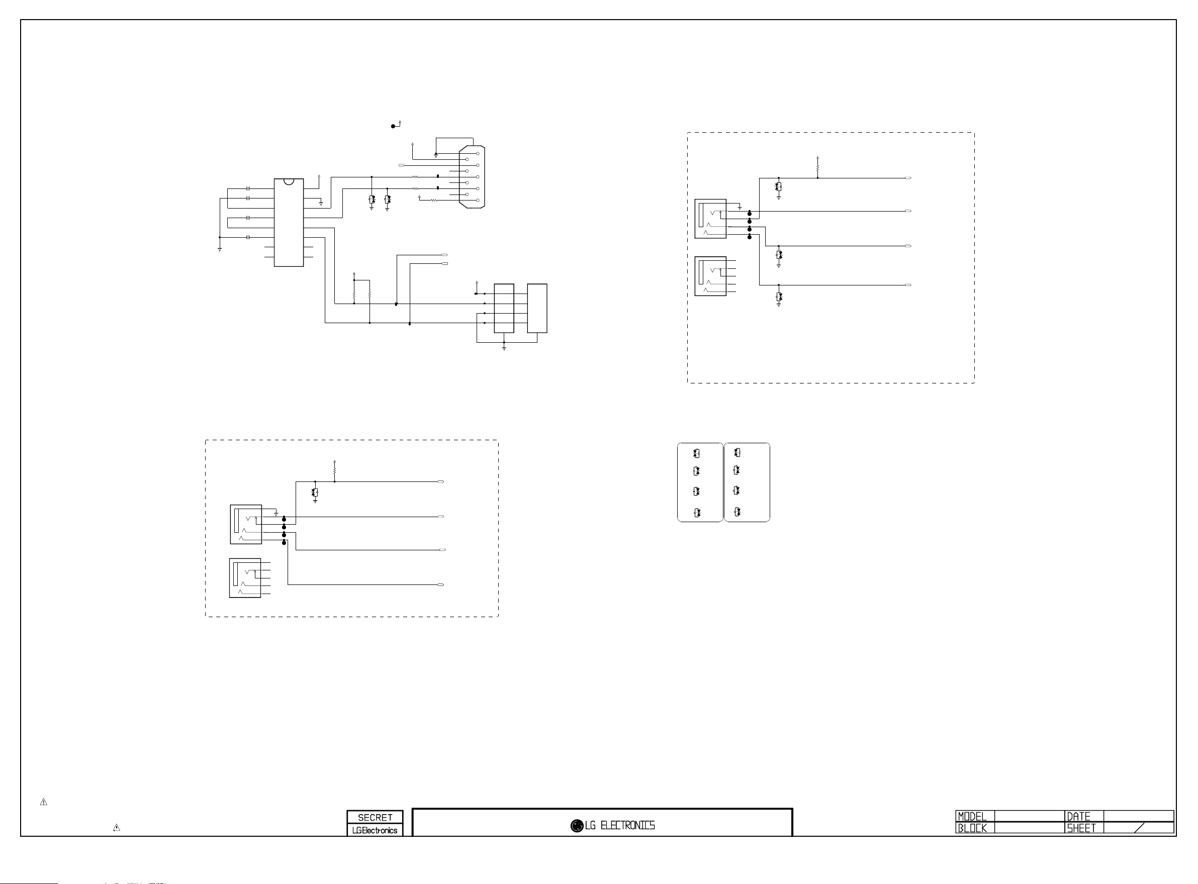
RS232C
Copyright ⓒ 2012 LG Electronics. Inc. All right reserved.
Only for training and service purposes
LGE Internal Use Only
0.1uF
0.1uF
RS232
RS232
RS232
RS232
C38000.1uF
C3801
C38020.1uF
C3803
DOUT2
12V_COMMERCIAL_OUT
12V 1A FOR COMMERCIAL(RS-232C POWER)
12V_COMMERCIAL_OUT
IC3800
+3.5V_ST
MAX3232CDR
C1+
V+
C1-
C2+
C2-
V-
RIN2
1
2
3
4
RS232
5
6
7
8
EAN41348201
VCC
16
GND
15
DOUT1
14
RIN1
13
ROUT1
12
DIN1
11
DIN2
10
ROUT2
9
+3.5V_ST
R3811
IR_OUT
RS232
100
R3820
RS232
100
R3821
+3.5V_ST
OPT_RS232
R3834
10K
FOR COMMERCIAL
R3814
D3805
20V
OPT
4.7K
OPT
D3804
20V
OPT
4.7K
OPT
SOC_RX
SOC_TX
10
9
8
7
6
RS232
SPG09-DB-009
JK3803
+3.5V_ST
5
4
3
2
1
UART_4PIN_STRAIGHT
P3800
12507WS-04L
1
2
3
4
5
UART_4PIN_ANGLE
P3801
12507WR-04L
1
2
3
4
5
CVBS 1 PHONE JACK
AV_JACK_BLACK
JK3800
KJA-PH-1-0177
5 M5_GND
4 M4
3 M3_DETECT
1 M1
6 M6
AV_JACK_YELLOW
JK3800-*1
KJA-PH-1-0177-1
5 M5_GND
4 M4
3 M3_DETECT
1 M1
6 M6
D3800
5.6V
OPT
D3801
5.6V
D3802
5.6V
+3.3V_NORMAL
R3810
10K
OPT
OPT
AV1_CVBS_DET
AV1_CVBS_IN
AV1_L_IN
AV1_R_IN
COMPONENT 1 PHONE JACK
COMP_JACK_BLACK
JK3801
KJA-PH-1-0177
5 M5_GND
4 M4
3 M3_DETECT
1 M1
6 M6
COMP_JACK_GREEN
JK3801-*1
KJA-PH-1-0177-2
5 M5_GND
4 M4
3 M3_DETECT
1 M1
6 M6
D3803
5.6V
OPT
+3.3V_NORMAL
R3806
10K
COMP1_DET
COMP1_Y
COMP1_Pb
COMP1_Pr
ESD For MTK ESD For LG1152
D3803-*1
5.6V
ESD_MTK
D3800-*1
5.6V
ESD_MTK
D3801-*1
5.6V
ESD_MTK
D3802-*1
5.6V
ESD_MTK
D3803-*2
5.6V
ESD_LG1152
D3800-*2
ESD_LG1152
D3801-*2
5.6V
ESD_LG1152
D3802-*2
5.6V
ESD_LG1152
5.6V
THE SYMBOL MARK OF THIS SCHEMETIC DIAGRAM INCORPORATES
SPECIAL FEATURES IMPORTANT FOR PROTECTION FROM X-RADIATION.
FILRE AND ELECTRICAL SHOCK HAZARDS, WHEN SERVICING IF IS
ESSENTIAL THAT ONLY MANUFATURES SPECFIED PARTS BE USED FOR
THE CRITICAL COMPONENTS IN THE SYMBOL MARK OF THE SCHEMETIC.
JACK_COMMON
2011.11.21
38
Page 30

IR
Copyright ⓒ 2012 LG Electronics. Inc. All right reserved.
Only for training and service purposes
LGE Internal Use Only
IR & KEY
COMMERCIAL
MMBT3904(NXP)
COMMERCIAL_IR
Q4100
+3.5V_ST
R4101
1K
IR_BYPASS
COMMERCIAL_IR
C
B
E
COMMERCIAL_IR
R4100
0
COMMERCIAL_IR
R4102
10K
MMBT3904(NXP)
COMMERCIAL_IR
R4103
Q4101
3.3K
+3.5V_ST
C
E
IR_OUT
R4104
47K
B
COMMERCIAL_IR
COMMERCIAL
R4105
22
COMMERCIAL_IR
COMMERCIAL_IR_EU
Q4102
MMBT3904(NXP)
COMMERCIAL_IR_EU
COMMERCIAL_IR_US
R4109
+3.5V_ST
R4107
10K
+3.5V_ST
1K
C
E
R4108
0
KEY1
KEY2
IR_BYPASS
COMMERCIAL_IR
COMMERCIAL_IR_EU
R4111
10K
B
MMBT3904(NXP)
COMMERCIAL_IR
R4115
Q4104
R4117
10K
5%
R4113
100
R4114
100
+3.5V_ST
3.3K
+3.5V_ST
C
B
E
R4118
10K
5%
R4119
47K
COMMERCIAL_IR
+3.5V_ST
C4100
0.1uF
D4100
5.6V
OPT
AMOTECH CO., LTD.
C4104
1000pF
50V
C4102
0.1uF
AMOTECH CO., LTD.
L4100
BLM18PG121SN1D
Soft Touch Micom D/L
Zener Diode is
close to wafer
RGB Sensor
D4101
5.6V
OPT
LED_B/GP4_LED_R
EEPROM_SCL
EEPROM_SDA
C4107
100pF
50V
R4123
100
R4124
100
R4125 1.5K
D4104
5.6V
D4105
ADUC 20S 02 010L
20V
OPT
D4106
ADUC 20S 02 010L
20V
OPT
OPT
AMOTECH CO., LTD.
GP4_IR_10P
P4102
12507WR-10L
1
2
3
4
5
6
7
8
9
10
11
THE SYMBOL MARK OF THIS SCHEMETIC DIAGRAM INCORPORATES
SPECIAL FEATURES IMPORTANT FOR PROTECTION FROM X-RADIATION.
FILRE AND ELECTRICAL SHOCK HAZARDS, WHEN SERVICING IF IS
ESSENTIAL THAT ONLY MANUFATURES SPECFIED PARTS BE USED FOR
THE CRITICAL COMPONENTS IN THE SYMBOL MARK OF THE SCHEMETIC.
ESD for MTK
D4105-*1
ADUC 20S 02 010L
10pF
20V
ESD_MTK
D4106-*1
ADUC 20S 02 010L
20V
10pF
ESD_MTK
D4100-*1
5.6V
ADMC 5M 02 200L
ESD_MTK
D4101-*1
5.6V
ADMC 5M 02 200L
ESD_MTK
D4104-*1
200pF
5.6V
ADMC 5M 02 200L
ESD_MTK
200pF
200pF
ESD for LG1152
D4100-*2
200pF
5.6V
ADMC 5M 02 200L
ESD_LG1152
D4101-*2
5.6V
200pF
ADMC 5M 02 200L
ESD_LG1152
D4104-*2
200pF
5.6V
ADMC 5M 02 200L
ESD_LG1152
IR / KEY
2011.11.21
41
Page 31
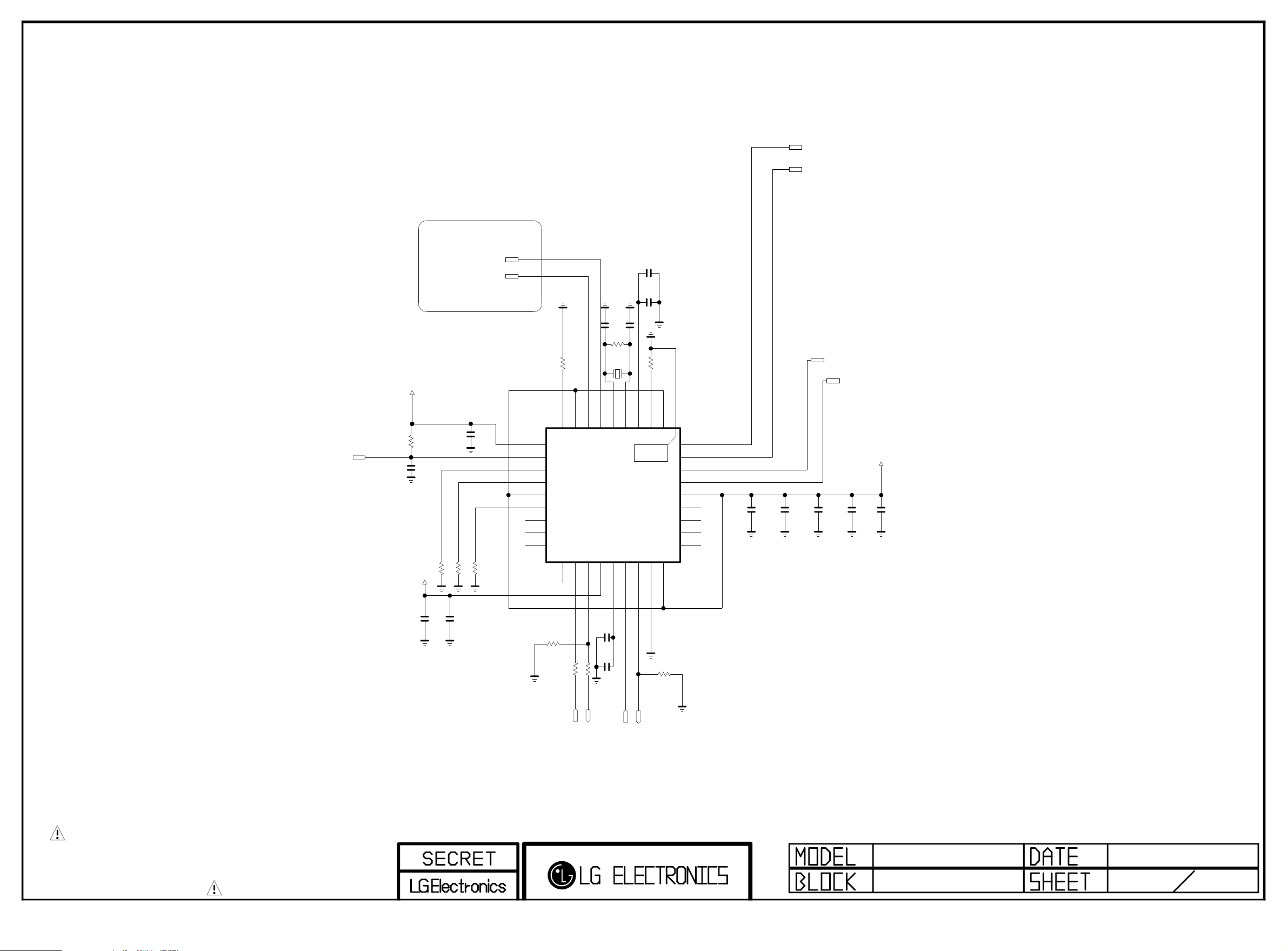
USB_DM1
Copyright ⓒ 2012 LG Electronics. Inc. All right reserved.
Only for training and service purposes
LGE Internal Use Only
USB_DP1
/RST_HUB
+3.3V_NORMAL
+3.3V_NORMAL
R4200
100K
C4200
0.1uF
OPT
USB_HUB_IC_IN_DP
USB_HUB_IC_IN_DM
C4203
0.1uF
HS_IND/CFG_SEL[1]
SCL/SMBCLK/CFG_SEL[0]
SDA/SMBDATA/NON_REM[1]
100K
R4201
R4202
100K
R4203
100K
VBUS_DET
RESET_N
VDD33_2
NC_8
NC_7
NC_6
C4205
15pF
C4207
15pF
R4205
1%
1M
X4200
R4204
100K
SUSP_IND/LOCAL_PWR/NON_REM[0]
28
27
26
25
24
23
22
USB HUB
21
20
19
18
NC_5
24MHz
VDDA33_330USBDM_UP31USBDP_UP32XTALOUT
29
IC4200
USB2512B-AEZG
14
15
16
17
CRFILT
VDD33_1
OCS_N[2]
C4209
1uF
25V
C4208
0.1uF
12K
1/16W 1%
XTALIN/CLKIN
PLLFILT35RBIAS36VDD33_3
33
34
THERMAL
37
11
12
13
TEST
OCS_N[1]
R4206
1
2
3
4
5
6
7
8
9
10
VDDA33_2
[EP]VSS
USBDM_DN[1]
USBDP_DN[1]
USBDM_DN[2]
USBDP_DN[2]
VDDA33_1
NC_1
NC_2
NC_3
NC_4
C4210
0.1uF
OPT
C4211
0.1uF
OPT
C4212
0.1uF
OPT
USB_DM2
C4213
0.1uF
USB_DP2
+3.3V_NORMAL
C4214
1uF
25V
C4201
4.7uF
C4202
0.1uF
R4209
100K
OPT
OPT
THE SYMBOL MARK OF THIS SCHEMETIC DIAGRAM INCORPORATES
SPECIAL FEATURES IMPORTANT FOR PROTECTION FROM X-RADIATION.
FILRE AND ELECTRICAL SHOCK HAZARDS, WHEN SERVICING IF IS
ESSENTIAL THAT ONLY MANUFATURES SPECFIED PARTS BE USED FOR
THE CRITICAL COMPONENTS IN THE SYMBOL MARK OF THE SCHEMETIC.
0.1uF
PRTPWR[2]/BC_EN[2]
1uF
25V
OPT
R4208 22
R4207 22
USB_CTL2
/USB_OCD2
C4204
C4206
PRTPWR[1]/BC_EN[1]
R4210
100K
OPT
USB_CTL1
/USB_OCD1
USB3_HUB
2011.06.13
42
Page 32
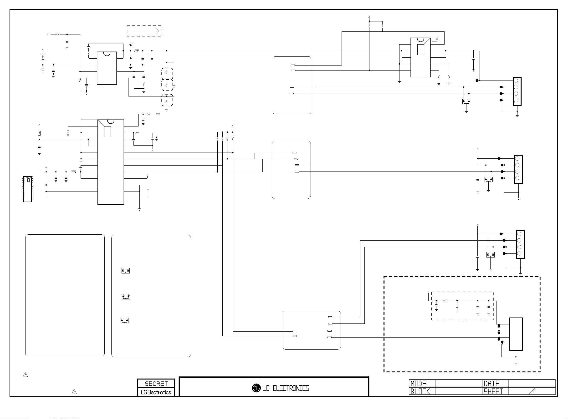
+5V_USB FOR USB1
Copyright ⓒ 2012 LG Electronics. Inc. All right reserved.
Only for training and service purposes
LGE Internal Use Only
POWER_ON/OFF2_4
+24V
L4305
BLM18PG121SN1D
C4324
10uF
35V
R4328
10K
C4327
0.1uF
16V
0.1uF
C4326
0.1uF
50V
OPT
Vout=0.8*(1+R1/R2)
330K
16V
R4329
C4329
0
BOOT
SS/TR
C4328
0.01uF
50V
R4330
VIN
EN
IC4305
TPS54331D
1
2
3
3A
4
+3.3V_NORMAL
R4327
R4323
10K
10K
MAX 2A
D4304-*1
40V
SX34
L4308
6.8uH
PH
8
D4304
SMAB34
GND
7
COMP
6
VSENSE
5
C4333
C4336
22uF
10V
C4334
4700pF
50V
R4336
20K
0.1uF
16V
/USB_OCD1
820
1%
R4343
R1
R2
OPT
C4338
1%
1000pF
R4338
10K
50V
1%
2K
R4339
USB_CTL1
USB_DM1
USB_DP1
40V
C4332
47pF
50V
OPT
IN_1
IN_2
ILIM_SEL
IC4303
TPS2554
GND
1
2
3
4
EN
5
11
THERMAL
[EP]
FAULT
10
OUT_2
9
1/10W
C4323
10uF
10V
OPT
OUT_1
8
ILIM0
7
ILIM1
6
R4300
27K
R4341
27K
1/10W
OPT
D4303
RCLAMP0502BA
USB1
DVR Ready
MAX 1.8A
3AU 04S-3 05-Z C-(LG )
JK4 303
1234
USB DOWN STR EAM
5
DEV_USB_DCDC_BD86180
IC4306-*1
BD86180MUV
EN
1
COMP
2
SS
3
RT
4
CTL2
5
CTL1
6
FLG2
7
FLG1
8
USB_OUT2
9
GND_1
10
GND_2
11
USB_OUT113USB_IN_1
12
+12V
L4306
BLM18PG121SN1D
C4325
10uF
16V
+5V_USB
[EP]GND
VREG
24
GND_3
25
23
THERMAL
VIN_2
22
VIN_1
21
PGND_2
20
PGND_1
19
BST
18
SW_2
17
SW_1
16
USB_IN_3
15
USB_IN_2
14
ESD for MTK
C4337
22uF
R4342
C4342
100pF
50V
R4332
10K
0.1uF
16V
10K
5%
C4340
4700pF
50V
IC4306
SN1104041, DC-DC+2CH USB SW
[EP]GND C4300
V7V
24
C4341
4.7uF
10V
L4307
3.6uH
C4301
22uF
10V
10V
C4331
0.1uF
16V
AGND_3
VIN_2
VIN_1
PGND_2
PGND_1
BST
LX_2
LX_1
SW_IN_3
SW_IN_2
SW_IN_1
THERMAL
25
23
22
21
20
19
18
17
16
15
14
13
EN
1
COMP
2
SS
3
ROSC
4
USB_DCDC_SN1104041
EN_SW2
5
EN_SW1
6
NFAULT2
7
NFAULT1
8
SW_OUT2
9
AGND_1
10
USB_DCDC_SN1104041
AGND_2
11
SW_OUT1
12
POWER_ON/OFF2_4
USB_DCDC_SN1104041
C4340-*1
0.01uF
50V
USB_DCDC_BD86180
+5V_USB_3
+5V_USB_2
10K
R4301
10K
R4302
+3.3V_NORMAL
10K
OPT
R4303
10K
R4304
OPT
USB_CTL2
/USB_OCD2
USB_DM2
USB_DP2
+5V_USB_2
C4322
10uF
10V
USB2
MAX 1.5A
3AU 04S-3 05-Z C-(LG )
OPT
D4302
RCLAMP0502BA
JK4 302
1234
USB DOWN STR EAM
5
USB3
+5V_USB_3
ESD for LG1152
MAX 1.5A
3AU 04S-3 05-Z C-(LG )
JK4 300
1234
D4300-*2
RCLAMP0502BA
ESD_LG1152
D4302-*1
RCLAMP0502BA
ESD_LG1152
D4303-*3
RCLAMP0502BA
ESD_LG1152
THE SYMBOL MARK OF THIS SCHEMETIC DIAGRAM INCORPORATES
SPECIAL FEATURES IMPORTANT FOR PROTECTION FROM X-RADIATION.
FILRE AND ELECTRICAL SHOCK HAZARDS, WHEN SERVICING IF IS
ESSENTIAL THAT ONLY MANUFATURES SPECFIED PARTS BE USED FOR
THE CRITICAL COMPONENTS IN THE SYMBOL MARK OF THE SCHEMETIC.
From SoC
USB_CTL3
/USB_OCD3
USB_DM3
USB_DP3
WIFI_DM
WIFI_DP
USB_WIFI
+5V_USB
L4302
WIFI120-ohm
BLM18PG121SN1D
C4319
0.1uF
16V
WIFI
For EMI
USB3_HUB_WiFi
C4320
0.1uF
16V
WIFI
C4310
10uF
C4321
10uF
WIFI
USB DOWN STR EAM
P4301
12507WR-04L
WIFI
1
2
3
4
5
.
5
OPT
D4300
10V
C4339
10uF
10V
10V
WIFI
RCLAMP0502BA
MAX 0.4A
VDD
DM
DP
GND
2011.10.26
43
Page 33
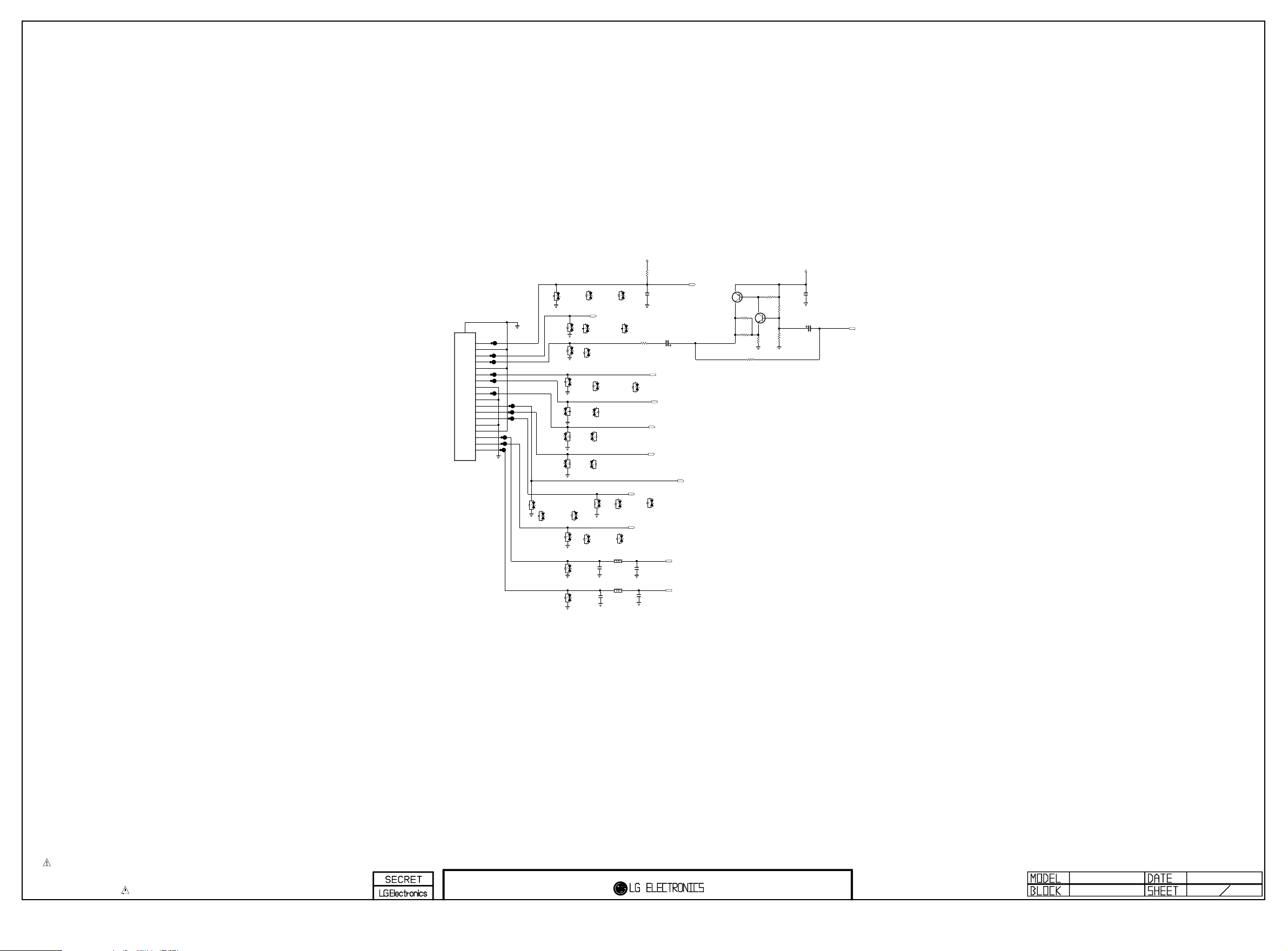
Full Scart(18 Pin Gender)
Copyright ⓒ 2012 LG Electronics. Inc. All right reserved.
Only for training and service purposes
LGE Internal Use Only
D4611
5.6V
OPT
D4609
D4600
20V
OPT
5.5V
OPT
D4610
5.5V
OPT
D4600-*1
20V
10pF
ESD_MTK_SCART
D4606
5.6V
OPT
D4607
5.6V
OPT
D4608
5.6V
OPT
D4603
5.5V
D4604
5.5V
D4601
5.6V
OPT
D4602
5.5V
OPT
OPT
OPT
19
DA1R018H91E
JK4600
EU
SHIELD
18
17
16
15
14
13
12
11
10
9
8
7
6
5
4
3
2
1
AV_DET
COM_GND
SYNC_IN
SYNC_OUT
SYNC_GND
RGB_IO
R_OUT
R_GND
G_OUT
G_GND
ID
B_OUT
AUDIO_L_IN
B_GND
AUDIO_GND
AUDIO_L_OUT
AUDIO_R_IN
AUDIO_R_OUT
D4611-*2
5.6V
200pF
ESD_LG1152_SCART
SC_CVBS_IN
D4609-*1
5.5V
15pF
ESD_MTK_SCART
D4610-*1
5.5V
15pF
ESD_MTK_SCART
15pF
ESD_MTK_SCART
D4603-*1
5.5V
15pF
ESD_MTK_SCART
D4604-*1
5.5V
15pF
ESD_MTK_SCART
D4600-*2
20V
10pF
ESD_LG1152_SCART
D4606-*1
5.6V
200pF
ESD_MTK_SCART
D4601-*1
5.6V
200pF
ESD_MTK_SCART
D4602-*1
5.5V
D4605
5.6V
OPT
BLM18PG121SN1D
EU
EU
C4600
1000pF
50V
BLM18PG121SN1D
EU
EU
C4601
1000pF
50V
D4611-*1
5.6V
200pF
ESD_MTK_SCART
D4609-*2
5.5V
15pF
ESD_LG1152_SCART
D4605-*1
5.6V
200pF
ESD_MTK_SCART
D4606-*2
5.6V
200pF
ESD_LG1152_SCART
L4600
L4601
+3.3V_NORMAL
EU
R4601
10K
EU
C4604
0.1uF
R460075
EU
D4601-*2
5.6V
200pF
ESD_LG1152_SCART
SC_L_IN
SC_R_IN
EU
C4602
4700pF
EU
C4603
4700pF
CLOSE TO JUNCTION
EU
C4605
100uF
16V
SC_FB
SC_R
SC_G
SC_B
D4605-*2
5.6V
200pF
ESD_LG1152_SCART
SC_ID
DTV/MNT_L_OUT
DTV/MNT_R_OUT
SC_DET
MMBT3906(NXP)
Gain=1+Rf/Rg
Q4600
+12V
EU
E
C
R4608
R4603
390
EU
R4602
390
Rf
B
EU
470
Q4601
MMBT3904(NXP)
C
E
Rg
R4604
180
0
OPT
EU
R4605
EU
R4606
47K
B
EU
R4607
15K
EU
C4606
0.1uF
50V
EU
EU
C4607
47uF
25V
EU
DTV/MNT_V_OUT
THE SYMBOL MARK OF THIS SCHEMETIC DIAGRAM INCORPORATES
SPECIAL FEATURES IMPORTANT FOR PROTECTION FROM X-RADIATION.
FILRE AND ELECTRICAL SHOCK HAZARDS, WHEN SERVICING IF IS
ESSENTIAL THAT ONLY MANUFATURES SPECFIED PARTS BE USED FOR
THE CRITICAL COMPONENTS IN THE SYMBOL MARK OF THE SCHEMETIC.
SCART GENDER
2011.10.26
46
Page 34
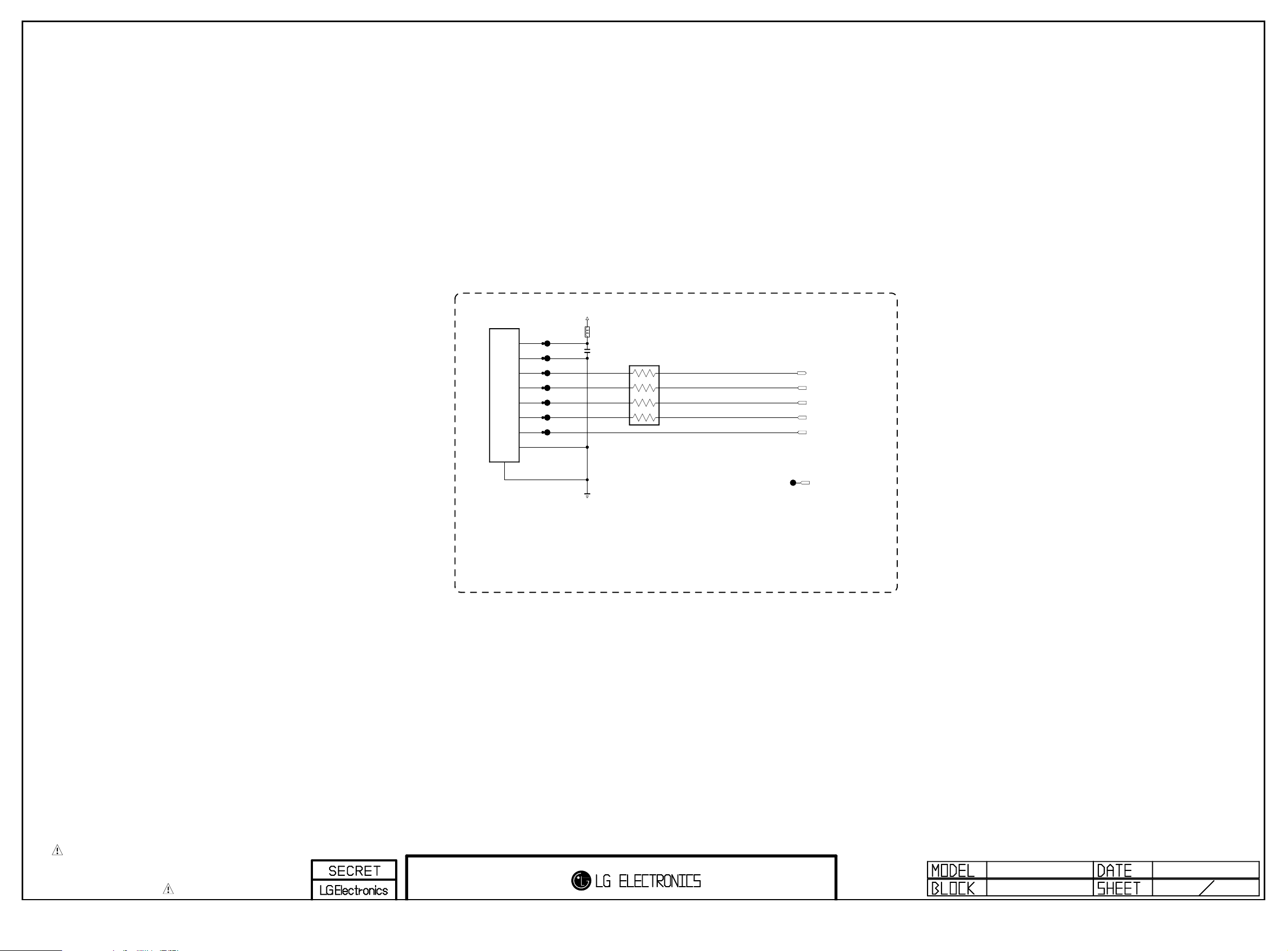
ZigBee_Radio Pulse M_REMOTE OPTION
Copyright ⓒ 2012 LG Electronics. Inc. All right reserved.
Only for training and service purposes
LGE Internal Use Only
P4800
12507WR-08L
M_REMOTE
9
+3.3V_NORMAL
L4800
120-ohm
3.3V
1
GND
2
RX
3
TX
4
RESET
5
DC
6
DD
7
GND
8
C4800
0.1uF
M_REMOTE
AR4800
100
1/16W
M_REMOTE
M_REMOTE_RX
M_REMOTE_TX
M_RFModule_RESET
M_RFModule_ISP
3D_SYNC_RF
Only For PDP
3D_SYNC_RF
ALL M_REMOTE OPTION
THE SYMBOL MARK OF THIS SCHEMETIC DIAGRAM INCORPORATES
SPECIAL FEATURES IMPORTANT FOR PROTECTION FROM X-RADIATION.
FILRE AND ELECTRICAL SHOCK HAZARDS, WHEN SERVICING IF IS
ESSENTIAL THAT ONLY MANUFATURES SPECFIED PARTS BE USED FOR
THE CRITICAL COMPONENTS IN THE SYMBOL MARK OF THE SCHEMETIC.
MOTION REMOTE
2011.11.21
48
Page 35
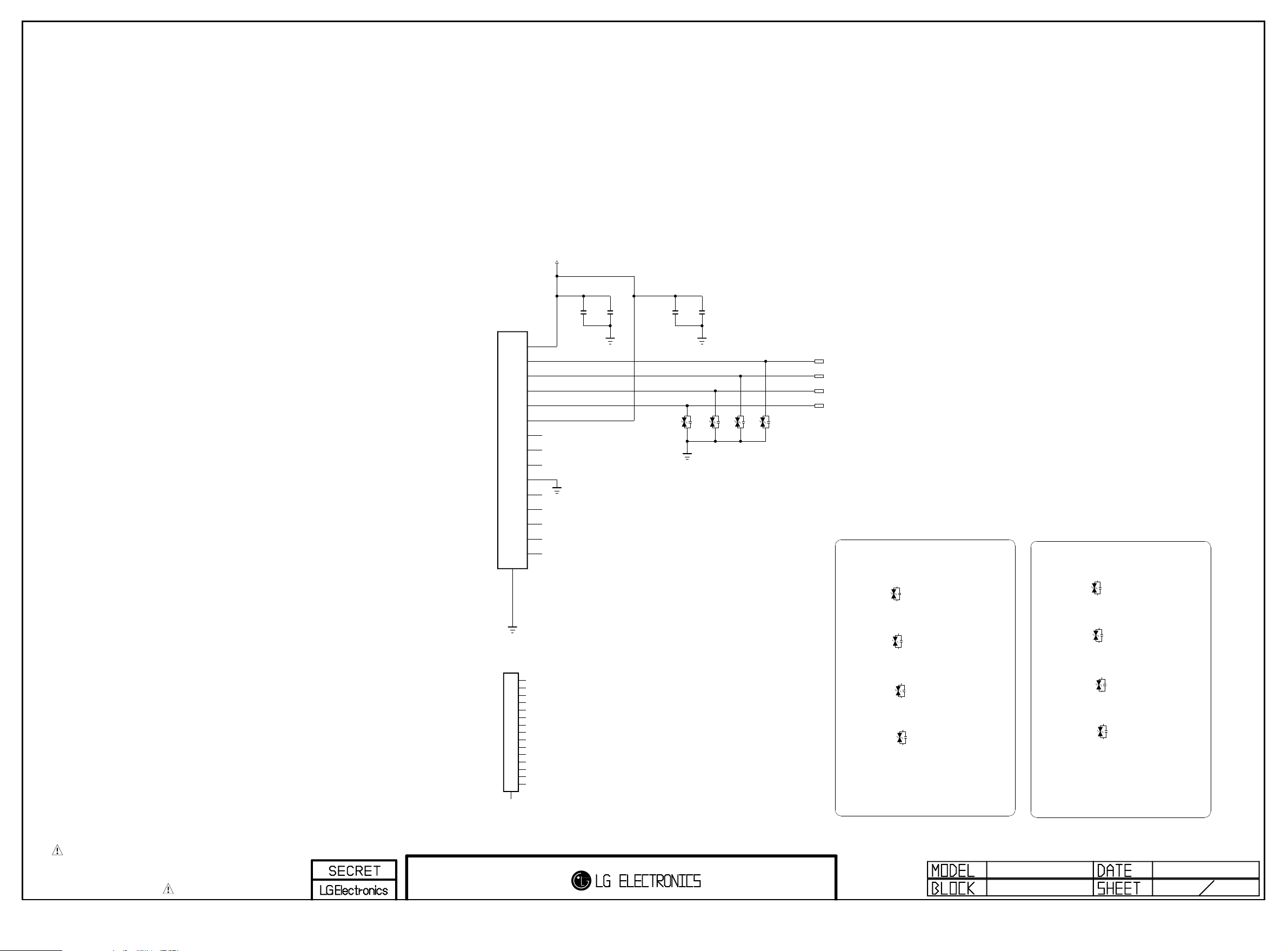
Ethernet Block
Copyright ⓒ 2012 LG Electronics. Inc. All right reserved.
Only for training and service purposes
LGE Internal Use Only
LAN_JACK_POWER
JK5000
XRJH-01A-4-DA7-180-LG(B)
LAN_XML
P1[CT]
1
P2[TD+]
2
P3[TD-]
3
P4[RD+]
4
P5[RD-]
5
P6[CT]
6
P7
7
P8
8
P9
9
P10[GND]
10
P11
11
YL_C
D1
YL_A
D2
GN_C
D3
GN_A
D4
12
SHIELD
JK5000-*1
TLA-6T764
LAN_TDK
R1
1
R2
2
R3
3
R4
4
R5
5
R6
6
R7
7
R8
8
R9
9
R10[GND]
10
R11
11
YL_C
D1
YL_A
D2
GN_C
D3
GN_A
D4
12
SHIELD
C5000
0.1uF
16V
C5001
0.01uF
50V
D5000
5.5V
OPT
C5002
0.1uF
16V
D5001
5.5V
OPT
C5003
0.01uF
50V
D5002
5.5V
EPHY_TDP
EPHY_TDN
EPHY_RDP
EPHY_RDN
D5003
5.5V
OPT
OPT
ESD for MTK
D5000-*1
ESD_MTK
ADUC 5S 02 0R5L
D5001-*1
ESD_MTK
ADUC 5S 02 0R5L
D5002-*1
ESD_MTK
ADUC 5S 02 0R5L
D5003-*1
ESD_MTK
ADUC 5S 02 0R5L
ESD for LG1152
ESD_LG1152
D5000-*2
5.5V
ADUC 5S 02 0R5L
ESD_LG1152
D5001-*2
5.5V
ADUC 5S 02 0R5L
ESD_LG1152
D5002-*2
5.5V
ADUC 5S 02 0R5L
ESD_LG1152
D5003-*2
5.5V
ADUC 5S 02 0R5L
THE SYMBOL MARK OF THIS SCHEMETIC DIAGRAM INCORPORATES
SPECIAL FEATURES IMPORTANT FOR PROTECTION FROM X-RADIATION.
FILRE AND ELECTRICAL SHOCK HAZARDS, WHEN SERVICING IF IS
ESSENTIAL THAT ONLY MANUFATURES SPECFIED PARTS BE USED FOR
THE CRITICAL COMPONENTS IN THE SYMBOL MARK OF THE SCHEMETIC.
LAN_VERTICAL
2011.12.09
50
Page 36
Ethernet Block
Copyright ⓒ 2012 LG Electronics. Inc. All right reserved.
Only for training and service purposes
LGE Internal Use Only
+3.3V_NORMAL
LAN_JACK_POWER
ET_COL/SNI
EPHY_TDP
EPHY_TDN
EPHY_RDP
EPHY_RDN
C5200
4.7uF
10V
Place 0.1uF close to each power pins
C5201
0.1uF
16V
Route Single 50 Ohm, Differential 100 Ohm
+3.3V_NORMAL
C5203
0.1uF
16V
25MHz, CL 18pF, ESR , max 30 Ohm, +/-30ppm
Place this cap. near IC
C5204
C5205
10uF
0.1uF
10V
16V
OPT
+3.3V_NORMAL
Place this Res. near IC
R5204
2.49K 1%
R5203
4.7K
C5206
15pF
50V
C5207
15pF
50V
AVDD10OUT
AVDD33_1
X5200
25MHZ
MDI+[0]
MDI-[0]
MDI+[1]
MDI-[1]
RSET
RXDV
R5205
0
Place this cap. near IC
+3.3V_NORMAL
AVDD33_2
CKXTAL1
CKXTAL2
[EP]
30
31
32
1
THERMAL
2
33
3
4
RTL8201F-VB-CG
5
6
7
8
9
11
RXD[0]10RXD[1]
RXD[2]/INTB
R5207 22
R5206 22
R5201 22
EPHY_RXD0
EPHY_RXD1
C5208
0.1uF
16V
ET_RXER
DVDD10OUT
29
IC5200
12
13
RXC
RXD[3]/CLK_CTL
C5209
56pF
4.7K
EPHY_INT
R5208
C5210
10uF
10V
OPT
EPHY_CRS_DV
ET_COL/SNI
CRS/CRS_DV
COL28RXER/FXEN
26
27
14
15
TXC
DVDD33
L5211
C5202
Place near IC
56pF
EPHY_ACTIVITY
R521022
LED1/PHYAD[1]
25
LED0/PHYAD[0]/PMEB
24
MDIO
23
MDC
22
PHYRSTB
21
TXEN
20
TXD[3]
19
TXD[2]
18
TXD[1]
17
16
+3.3V_NORMAL
TXD[0]
100NH
EPHY_TXD0
C5211
0.1uF
16V
EPHY_LINK
EPHY_MDC
EPHY_EN
EPHY_TXD1
+3.3V_NORMAL
R5212
1.5K
1/16W
C5212
0.1uF
OPT
+3.3V_NORMAL
4.7K
4.7K
R5216
R5215
4.7K
R5217
5%
EPHY_MDIO
/RST_PHY
EPHY_LINK
EPHY_ACTIVITY
ET_RXER
THE SYMBOL MARK OF THIS SCHEMETIC DIAGRAM INCORPORATES
SPECIAL FEATURES IMPORTANT FOR PROTECTION FROM X-RADIATION.
FILRE AND ELECTRICAL SHOCK HAZARDS, WHEN SERVICING IF IS
ESSENTIAL THAT ONLY MANUFATURES SPECFIED PARTS BE USED FOR
THE CRITICAL COMPONENTS IN THE SYMBOL MARK OF THE SCHEMETIC.
EPHY_REFCLK
LG1152 A0
14ETHERNET 50
Page 37
Q1801
Copyright ⓒ 2012 LG Electronics. Inc. All right reserved.
Only for training and service purposes
LGE Internal Use Only
AMP_MUTE
DUAL COMPONENT
1ST : 0TRIY80001A 2ND : 0TR387500AA
L5400
CIS21J121
+24V_AMP
AUD_LRCH
AUD_LRCK
AUD_SCK
I2C_SDA1
I2C_SCL1
R5400
10K
C5401
0.1uF
50V
+3.3V_NORMAL
B
+24V
C5400
0.1uF
50V
C5402
100pF
50V
R5402 100
R5403 100
R5401
10K
C
Q5400
MMBT3904(NXP)
E
R5405
100
C5403
1000pF
50V
R5404
3.3K
1000pF
C5404
+3.3V_NORMAL
L5401
BLM18PG121SN1D
C5413
0.1uF
16V
C5407
4.7uF
10V
C5408
33pF
50V
OPT
C5409
10uF
10V
OPT
C5410
10uF
10V
C5411
0.1uF
16V
C5412
0.1uF
16V
OPT
C5405
10uF
10V
C5406
33pF
50V
50V
AMP_RESET_N
AUD_MASTER_CLK
C5414
10uF
10V
AGND_PLL
AVDD_PLL
DVDD_PLL
LF
DGND_PLL
GND_1
DGND
DVDD
SDATA
WCK
BCK
SDA
C5415
1000pF
50V
[EP]
1
2
3
4
5
6
7
8
9
10
11
12
GND_IO
CLK_I
VDD_IO
46
47
48
THERMAL
49
NTP-7500L
13
14
15
SCL
/FAULT
MONITOR0
50V
C5416
BST1A
/RESET
AD
43
44
45
IC5400
0x54
16
17
18
BST2B
MONITOR1
MONITOR2
C5417
22000pF
50V
22000pF
OUT1A_2
PGND1A
41
42
19
20
PGND2B
OUT2B_1
PVDD1_2
PVDD1_3
OUT1A_1
38
39
40
21
22
23
OUT2B_2
PVDD2_1
PVDD2_2
+24V_AMP
C5418
0.1uF
50V
PVDD1_1
37
36
35
34
33
32
31
30
29
28
27
26
25
24
PVDD2_3
C5420
0.1uF
50V
OUT1B_2
OUT1B_1
PGND1B
BST1B
VDR1
VCC_5
AGND
VDR2
BST2A
PGND2A
OUT2A_2
OUT2A_1
+24V_AMP
C5419
0.1uF
50V
C5421
0.1uF
50V
R5406
3.3
C5422
10uF
35V
OPT
OPT
C5424
0.01uF
50V
C5423
10uF
35V
C5425
22000pF
50V
C5426
22000pF
50V
C54 27
1uF
25V
D5400
1N4148W
100V
OPT
D5401
1N4148W
100V
OPT
D5402
1N4148W
100V
OPT
D5403
1N4148W
100V
OPT
C54 28
1uF
25V
R5407
12
C5429
390pF
50V
C5430
390pF
50V
R5408
12
R5409
12
C5431
390pF
50V
C5432
390pF
50V
R5410
12
C5433
1uF
25V
R5414
12
R5412
12
R5413
12
R5411
12
L5404
10.0uH
NRS6045T100MMGK
L5405
10.0uH
NRS6045T100MMGK
L5402
10.0uH
NRS6045T100MMGK
L5403
10.0uH
NRS6045T100MMGK
C5434
0.47uF
50V
C5435
0.47uF
50V
C5436
0.1uF
50V
C5437
0.1uF
50V
C5438
0.1uF
50V
C5439
0.1uF
50V
R5415
5.1K
R5416
5.1K
R5417
5.1K
R5418
5.1K
SPK_L+
SPEAKER_L
SPK_L-
SPK_L+
SPK_L-
SPK_R+
SPK_R-
SPK_R+
SPEAKER_R
SPK_R-
WAFER-ANGLE
4
3
2
1
P5400
WOOFER_MUTE
WOOFER_MUTE
TP5403
THE SYMBOL MARK OF THIS SCHEMETIC DIAGRAM INCORPORATES
SPECIAL FEATURES IMPORTANT FOR PROTECTION FROM X-RADIATION.
FILRE AND ELECTRICAL SHOCK HAZARDS, WHEN SERVICING IF IS
ESSENTIAL THAT ONLY MANUFATURES SPECFIED PARTS BE USED FOR
THE CRITICAL COMPONENTS IN THE SYMBOL MARK OF THE SCHEMETIC.
AMP_NEO
2011.11.21
54
Page 38
+24V
Copyright ⓒ 2012 LG Electronics. Inc. All right reserved.
Only for training and service purposes
LGE Internal Use Only
L5501
CIS21J121
WOOFER
+24V_AMP_WOOFER
C5529
0.1uF
50V
WOOFER
WOOFER AMP.
AUD_LRCH
AUD_LRCK
AUD_SCK
I2C_SDA1
I2C_SCL1
WOOFER
C5500
100pF
50V
R5501 100
R5502 100
WOOFER
WOOFER
WOOFER
C5501
1000pF
50V
WOOFER
R5503
3.3K
WOOFER
C5502
10uF
10V
C5503
33pF
50V
+3.3V_NORMAL
WOOFER
L5500
BLM18PG121SN1D
WOOFER
C5511
0.1uF
16V
WOOFER
C5504
OPT
4.7uF
10V
C5505
33pF
50V
WOOFER
WOOFER_MUTE
C5506
10uF
10V
C5507
10uF
WOOFER
OPT
C5508
0.1uF
16V
OPT
WOOFER
C5509
0.1uF
10V
16V
WOOFER
R5504
WOOFER
100
C5510
1000pF
50V
AMP_RESET_N
WOOFER
R5505
10K
AUD_MASTER_CLK
WOOFER
C5512
10uF
10V
AGND_PLL
AVDD_PLL
DVDD_PLL
DGND_PLL
GND_1
DGND
DVDD
SDATA
WCK
BCK
SDA
LF
WOOFER
C5513
1000pF
1
2
3
4
5
6
7
8
9
10
11
12
50V
[EP]
GND_IO
CLK_I
VDD_IO
46
47
48
THERMAL
49
NTP-7500L
13
14
15
SCL
/FAULT
MONITOR0
WOOFER
50V
C5514
BST1A
/RESET
AD
43
44
45
WOOFER
IC5500
16
17
18
BST2B
MONITOR1
MONITOR2
WOOFER
C5515
22000pF
50V
22000pF
OUT1A_2
PGND1A
41
42
19
20
PGND2B
OUT2B_1
PVDD1_2
PVDD1_3
OUT1A_1
38
39
40
21
22
23
OUT2B_2
PVDD2_1
PVDD2_2
+24V_AMP_WOOFER
WOOFER
C5516
0.1uF
50V
PVDD1_1
37
36
35
34
33
32
31
30
29
28
27
26
25
24
WOOFER
PVDD2_3
C5517
0.1uF
50V
WOOFER
C5518
0.1uF
50V
OUT1B_2
OUT1B_1
PGND1B
BST1B
VDR1
VCC_5
AGND
VDR2
BST2A
PGND2A
OUT2A_2
OUT2A_1
+24V_AMP_WOOFER
WOOFER
C5519
0.1uF
50V
OPT
R5506
3.3
WOOFER
C5520
10uF
35V
OPT
C5522
0.01uF
50V
WOOFER
C5521
10uF
35V
WOOFER
C5523
22000pF
50V
WOOFER
C5524
22000pF
50V
5%
4.7K
R5517
1/16W
WOOFER_MONO
WOOFER
C55 25
1uF
25V
WOOFER
C55 26
1uF
25V
WOOFER
C5531
1uF
25V
1N4148W
100V
OPT
D5501
1N4148W
OPT
1N4148W
OPT
1N4148W
OPT
D5500
100V
D5502
100V
D5503
100V
WOOFER_STEREO
WOOFER
R5507
12
WOOFER
C5527
390pF
50V
WOOFER
C5528
390pF
50V
WOOFER
R5508
12
WOOFER_STEREO
R5500
12
C5530
390pF
50V
WOOFER_STEREO
WOOFER_STEREO
C5533
390pF
50V
R5509
12
WOOFER_STEREO
WOOFER
R5514
12
WOOFER
R5512
12
WOOFER_STEREO
R5511
12
R5510
12
L5503
10.0uH
NRS6045T100MMGK
L5504
10.0uH
NRS6045T100MMGK
WOOFER_STEREO
L5502
10.0uH
NRS6045T100MMGK
WOOFER_STEREO
L5505
10.0uH
NRS6045T100MMGK
WOOFER
WOOFER
WOOFER
C5532
0.47uF
50V
WOOFER_STEREO
C5536
0.47uF
50V
SPK_WOOFER_L-
SPK_WOOFER_L+
WOOFER
C5534
0.1uF
50V
WOOFER
C5535
0.1uF
50V
SPK_WOOFER_R-
SPK_WOOFER_R+
WOOFER_STEREO
C5537
0.1uF
50V
WOOFER_STEREO
C5538
0.1uF
50V
WOOFER
R5515
5.1K
WOOFER
R5516
5.1K
WOOFER_STEREO
R5513
5.1K
WOOFER_STEREO
R5519
5.1K
SPK_WOOFER_L+
SPK_WOOFER_L-
SPK_WOOFER_R+
SPK_WOOFER_R-
P5500
FW25001-02(SPK 2P)
WOOFER
1
2
P5501
FW25003_03
1
2
3
DEV_WOOFER_STEREO
THE SYMBOL MARK OF THIS SCHEMETIC DIAGRAM INCORPORATES
SPECIAL FEATURES IMPORTANT FOR PROTECTION FROM X-RADIATION.
FILRE AND ELECTRICAL SHOCK HAZARDS, WHEN SERVICING IF IS
ESSENTIAL THAT ONLY MANUFATURES SPECFIED PARTS BE USED FOR
THE CRITICAL COMPONENTS IN THE SYMBOL MARK OF THE SCHEMETIC.
5%
1/16W
4.7K
R5518
WOOFER_MONO
Page 39
AUD_OUT >> EU/CHINA_HOTEL_OPT
Copyright ⓒ 2012 LG Electronics. Inc. All right reserved.
Only for training and service purposes
LGE Internal Use Only
DTV/MNT_L_OUT
EU
C6000
1uF
25V
OPT
C6002
6800pF
EU
R60002.2K
R6002
OPT
470K
SCART_AMP_L_FB
SCART_Lout
33pF
+12V
EU
IC6000
AZ4580MTR-E1
EU
VCC
8
OUT2
7
IN2-
6
IN2+
5
OUT1
EU
R600433K
C6003
EU
IN1-
IN1+
1
2
3
VEE
4
L6000
EU
C6004
0.1uF
50V
SIGN600005
R6008 33K
C6005
33pF
EU
EU
SCART_AMP_R_FB
SCART_Rout
OPT
R6010
470K
R6011
OPT
C6007
6800pF
2.2K
EU
C6008
1uF
25V
EU
DTV/MNT_R_OUT
[SCART AUDIO MUTE]
DTV/MNT_L_OUT
Q6000
MMBT3904(NXP)
DTV/MNT_R_OUT
Q6001
MMBT3904(NXP)
C
B
EU
E
C
B
EU
E
R6013
510
+3.5V_ST
EU
R6012
4.7K
OPT
SCART_MUTE
THE SYMBOL MARK OF THIS SCHEMETIC DIAGRAM INCORPORATES
SPECIAL FEATURES IMPORTANT FOR PROTECTION FROM X-RADIATION.
FILRE AND ELECTRICAL SHOCK HAZARDS, WHEN SERVICING IF IS
ESSENTIAL THAT ONLY MANUFATURES SPECFIED PARTS BE USED FOR
THE CRITICAL COMPONENTS IN THE SYMBOL MARK OF THE SCHEMETIC.
SCART AUDIO AMP
2011.11.21
60
Page 40
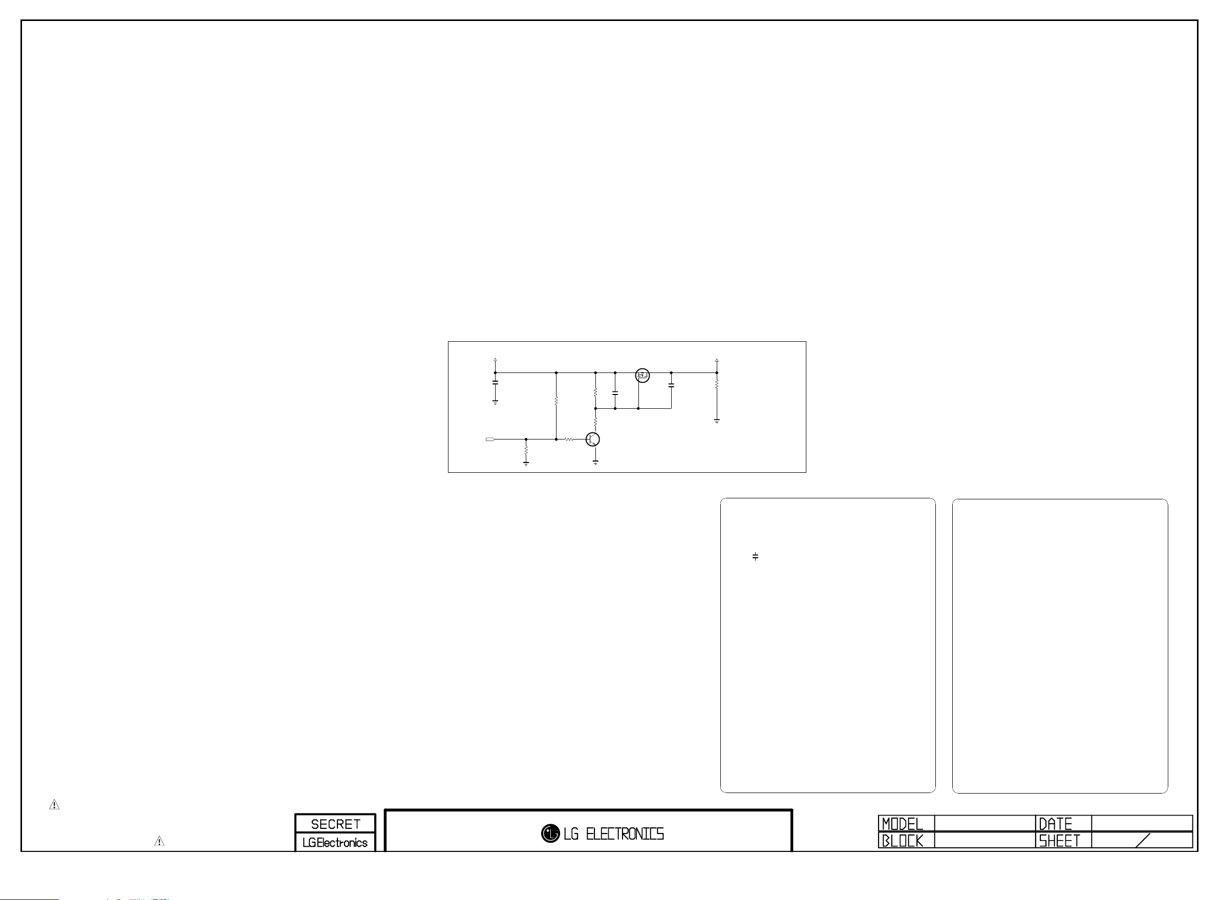
CI POWER ENABLE CONTROL
Copyright ⓒ 2012 LG Electronics. Inc. All right reserved.
Only for training and service purposes
LGE Internal Use Only
+5V_NORMAL
C6202
OPT
0.1uF
16V
PCM_5V_CTL
R6218
10K
CI
R6221
10K
OPT
R6223
4.7K
CI
B
CI
C
E
R6241
22K
R6242
2.2K
CI
Q6200
MMBT3904(NXP)
CI
C6207
4.7uF
10V
OPT
CI
Q6201
AO3407A
S
+5V_CI_ON
D
G
C6210
1uF
25V
OPT
R6248
10K
CI
THE SYMBOL MARK OF THIS SCHEMETIC DIAGRAM INCORPORATES
SPECIAL FEATURES IMPORTANT FOR PROTECTION FROM X-RADIATION.
FILRE AND ELECTRICAL SHOCK HAZARDS, WHEN SERVICING IF IS
ESSENTIAL THAT ONLY MANUFATURES SPECFIED PARTS BE USED FOR
THE CRITICAL COMPONENTS IN THE SYMBOL MARK OF THE SCHEMETIC.
Option FOR MTK
C6210-*1
1uF
25V
CI_MTK
Option FOR LG1152
CI SLOT
2011.10.31
62
Page 41
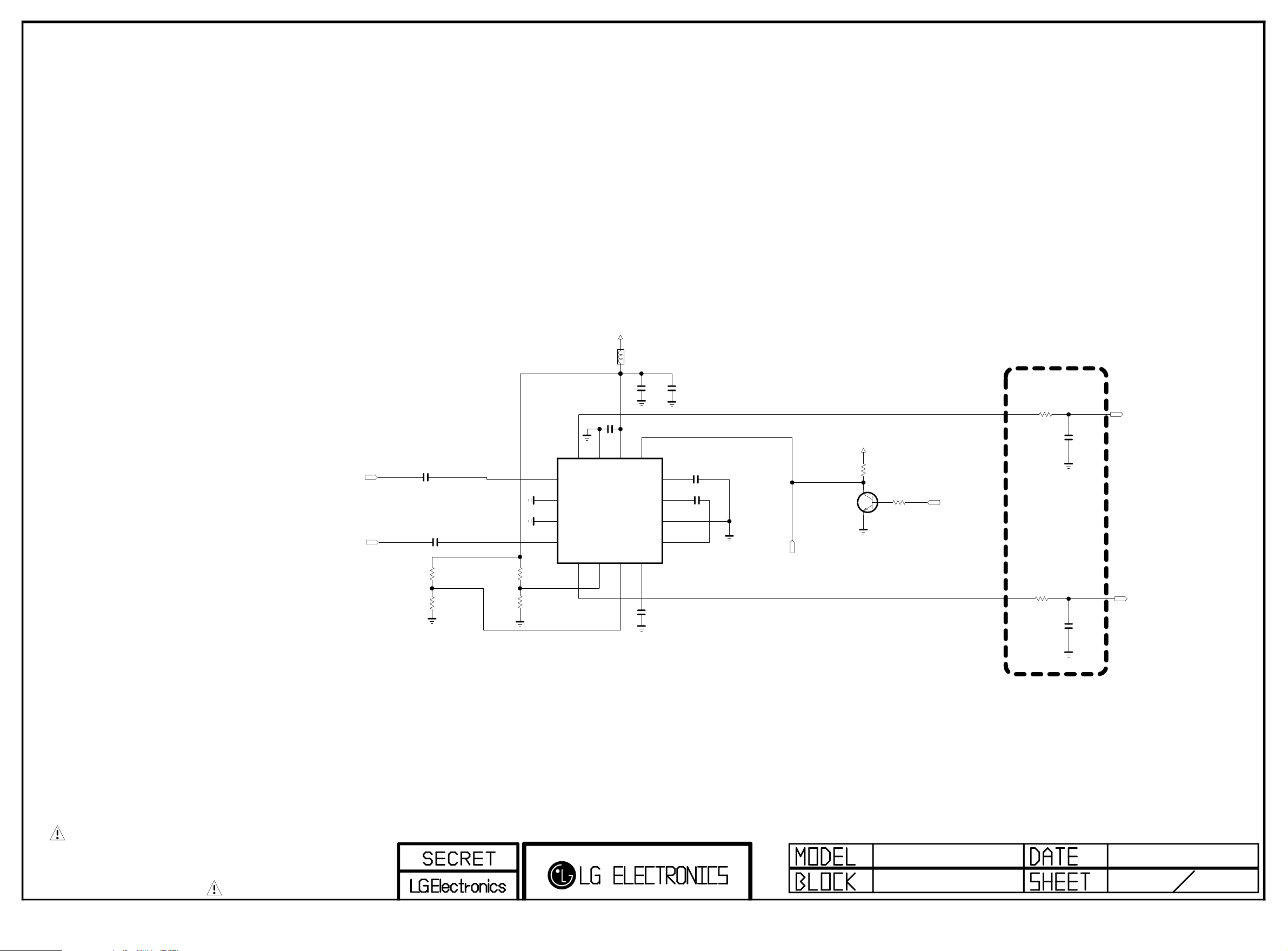
+3.3V_NORMAL
Copyright ⓒ 2012 LG Electronics. Inc. All right reserved.
Only for training and service purposes
LGE Internal Use Only
EARPHONE AMP
HP_LOUT_MAIN
HP_ROUT_MAIN
4.7K
R6400
OPT
R6401
C6400
1uF
10V
C6401
1uF
10V
OPT
R6402
4.7K
R6403
4.7K
Close to the IC
INL-
1
INL+
2
INR+
3
INR-
4
OUTL
16
5
OUTR
VDD
SGND
14
15
IC6400
TPA6132A2
EAN60724701
6G07G18
L6400
120-ohm
BLM18P G12 1SN1D
C6403
10uF
10V
C6402
1uF
10V
EN
13
12
11
10
9
HPVSS
C6404
2.2uF
10V
HPVDD
CPP
PGND
CPN
C6405
0.1uF
16V
C6406
2.2uF
10V
C6407
2.2uF
10V
MMBT3904(NXP)
HP_AMP_MUTE
Q6400
+3.3V_NORMAL
R6404
4.7K
C
B
E
R6405
1K
Place Near jack Side
SIDE_HP_MUTE
From Micom
R6406
10
1/16W
5%
R6407
10
1/16W
5%
C6408
0.47uF
16V
C6409
0.47uF
16V
HP_LOUT
HP_ROUT
THE SYMBOL MARK OF THIS SCHEMETIC DIAGRAM INCORPORATES
SPECIAL FEATURES IMPORTANT FOR PROTECTION FROM X-RADIATION.
FILRE AND ELECTRICAL SHOCK HAZARDS, WHEN SERVICING IF IS
ESSENTIAL THAT ONLY MANUFATURES SPECFIED PARTS BE USED FOR
THE CRITICAL COMPONENTS IN THE SYMBOL MARK OF THE SCHEMETIC.
HEADPHONE AMP
Low Pass Filter
2011.06.29
61
Page 42
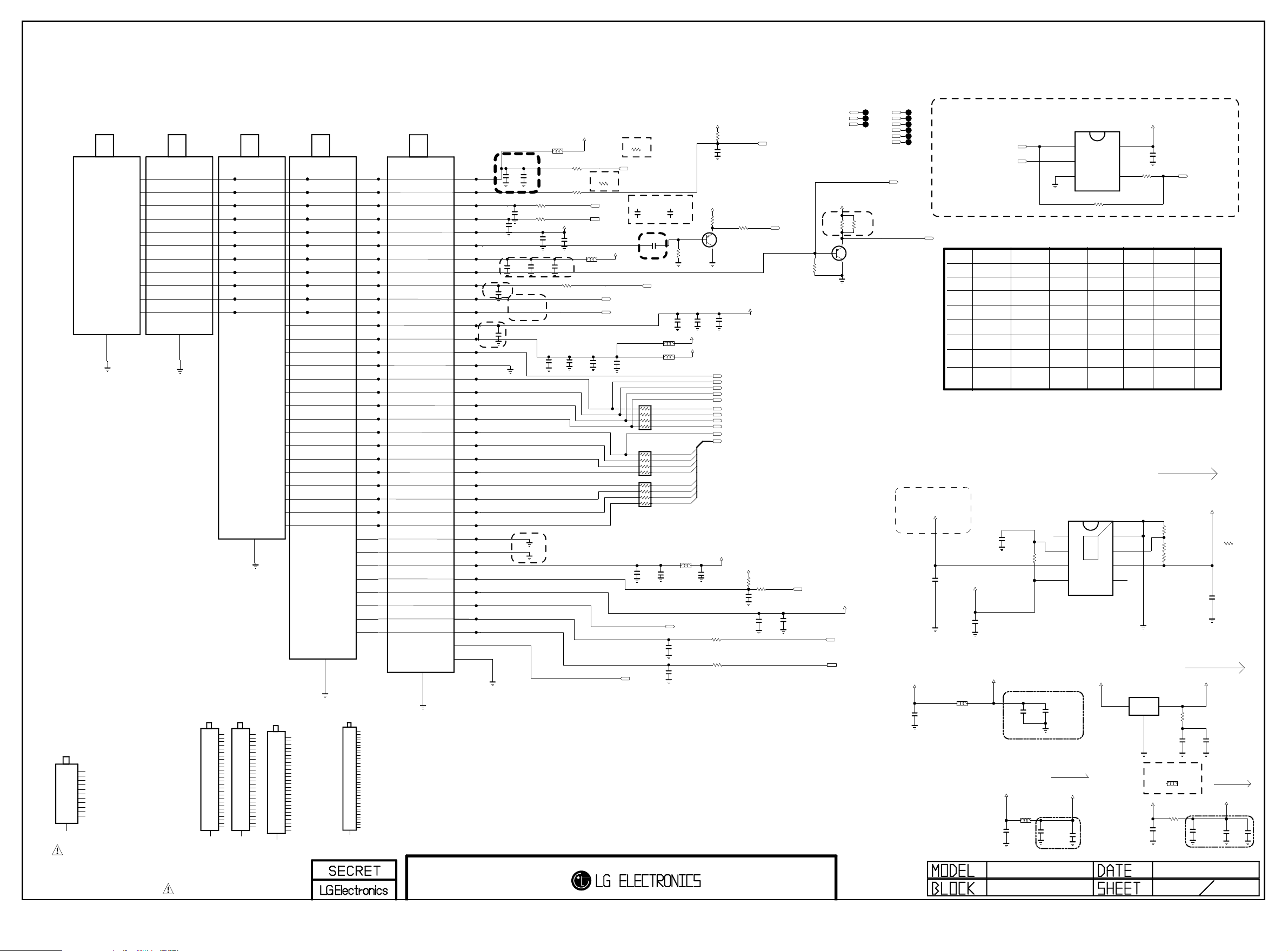
T/C/S & H/NIM & T2/C TUNER(EU & CHINA)
Copyright ⓒ 2012 LG Electronics. Inc. All right reserved.
Only for training and service purposes
LGE Internal Use Only
TU6504
TDSH-T151F
TW_H/NIM
RF_S/W_CTL
RESET
SCL
SDA
+B1[3.3V]
SIF
+B2[1.8V]
CVBS
IF_AGC
DIF[P]
DIF[N]
12
SHIELD
TDSS-G151D
1
2
3
4
5
6
7
8
9
10
11
TU6500
T/C_H/NIM_V
NC
RESET
SCL
SDA
+B1[3.3V]
SIF
+B2[1.8V]
CVBS
IF_AGC
DIF[P]
DIF[N]
12
SHIELD
1
2
3
4
5
6
7
8
9
10
11
TU6501
TDSN-G351D
T2/C_F/NIM_DEV
NC_1
RESET
SCL
SDA
+B1[3.3V]
SIF
+B2[1.8V]
CVBS
NC_2
NC_3
NC_4
+B3[3.3V]
+B4[1.23V]
NC_5
GND
ERROR
SYNC
VALID
MCLK
D0
D1
D2
D3
D4
D5
D6
D7
28
SHIELD
TDSQ-H051F
+5V[SPLITTER]
1
RESET
2
TU_SCL
3
TU_SDA
4
M_+3.3V
5
M_SIF
6
M_+1.8V
7
M_CVBS
8
M_IF_AGC
9
M_DIF[P]
10
M_DIF[N]
11
S_3.3V
12
S_1.8V
13
S_CVBS
14
GND_1
15
SD_ERROR
16
SD_SYNC
17
SD_VALID
18
SD_MCLK
19
SD_SERIAL_D0
20
N.C_1
21
N.C_2
22
N.C_3
23
N.C_4
24
N.C_5
25
N.C_6
26
N.C_7
27
GND_2
GND_3
SD_1.23V_DEMOD
SD_RESET
SD_3.3V_DEMOD
N.C_8
SD_SCL
SD_SDA
TU6502
CHB_V
1
2
3
4
5
6
7
8
9
10
11
12
13
14
15
16
17
18
19
20
21
22
23
24
25
26
27
28
29
30
31
32
33
34
35
36
RF_SWITCH_CTL USE: T2/C,T/C,ATSC,DTMB.ISDB-T
TU6503
TDSQ-G051D
T/C/S2_V
N.C_1
RESET
SCL
SDA
+3.3V_TUNER
SIF
+1.8V_TUNER
CVBS
T/C_IF_AGC
T/C_DIF[P]
T/C_DIF[N]
N.C_2
N.C_3
N.C_4
GND_1
ERROR
SYNC
VALID
MCLK
D0
D1
D2
D3
D4
D5
D6
D7
GND_2
GND_3
+1.23V_S2_DEMOD
S2_RESET
+3.3V_S2_DEMOD
S2_F22_OUTPUT
S2_SCL
S2_SDA
LNB
GND_4
SHIELD
BR_F/NIM_V
CN_ATBM
TU6501-*1
TU6501-*2
TDSN-B051F
TDSN-C251D
RF_S/W_CTL
1
1
RESET
2
2
SCL
3
3
SDA
4
4
+B1[3.3V]
5
5
SIF
6
6
+B2[1.8V]
7
AT_H/NIM_V
TU6500-*1
TDSS-H151F
NC
1
RESET
2
SCL
3
SDA
4
+B1[3.3V]
5
SIF
6
+B2[1.8V]
7
CVBS
8
IF_AGC
9
DIF[P]
10
DIF[N]
11
12
SHIELD
28
SHIELD
7
CVBS
8
8
NC_1
9
9
NC_2
10
10
NC_3
11
11
+B3[3.3V]
12
12
+B4[1.23V]
13
13
NC_4
14
14
GND
15
15
ERROR
16
16
SYNC
17
17
VALID
18
18
MCLK
19
19
D0
20
20
D1
21
21
D2
22
22
D3
23
23
D4
24
24
D5
25
25
D6
26
26
D7
27
27
28
SHIELD
RF_S/W_CTL
RESET
SCL
SDA
+B1[3.3V]
SIF
+B2[1.8V]
CVBS
NC_1
NC_2
NC_3
+B3[3.3V]
+B4[1.23V]
NC_4
GND
ERROR
SYNC
VALID
MCLK
D0
D1
D2
D3
D4
D5
D6
D7
28
SHIELD
CN_LG3921
TU6501-*3
TDSN-C051D
RF_S/W_CTL
1
RESET
2
SCL
3
SDA
4
+B1[3.3V]
5
SIF
6
+B2[1.8V]
7
CVBS
8
NC_1
9
NC_2
10
NC_3
11
+B3[3.3V]
12
+B4[1.23V]
13
NC_4
14
GND
15
ERROR
16
SYNC
17
VALID
18
MCLK
19
D0
20
D1
21
D2
22
D3
23
D4
24
D5
25
D6
26
D7
27
T2/C/S2
TU6503-*1
TDSQ-G351D
N.C_1
1
RESET
2
SCL
3
SDA
4
+B1[3.3V]
5
SIF
6
+B2[1.8V]
7
CVBS
8
N.C_2
9
N.C_3
10
N.C_4
11
+B3[3.3V]
12
+B4[1.23V]
13
N.C_5
14
GND_1
15
ERROR
16
SYNC
17
VALID
18
MCLK
19
D0
20
D1
21
D2
22
D3
23
D4
24
D5
25
D6
26
D7
27
GND_2
28
GND_3
29
+B5[1.23V]
30
S2_RESET
31
+B6[3.3V]
32
S2_F22_OUTPUT
33
S2_SCL
34
S2_SDA
35
LNB
36
GND_4
37
38
SHIELD
THE SYMBOL MARK OF THIS SCHEMETIC DIAGRAM INCORPORATES
SPECIAL FEATURES IMPORTANT FOR PROTECTION FROM X-RADIATION.
FILRE AND ELECTRICAL SHOCK HAZARDS, WHEN SERVICING IF IS
ESSENTIAL THAT ONLY MANUFATURES SPECFIED PARTS BE USED FOR
THE CRITICAL COMPONENTS IN THE SYMBOL MARK OF THE SCHEMETIC.
38
10
11
12
13
14
15
16
17
18
19
20
21
22
23
24
25
26
27
28
29
30
31
32
33
34
35
36
37
SHIELD
close to TUNER
1
2
3
4
5
6
7
8
9
OPT
close to Tuner
C6500
L9 ATSC
C6509
0.1uF
16V
CHB
close to TUNER
CHB
L6508
BLM18PG121SN1D
CHB
RF_SWITCH
C6501
C6503
10uF
0.1uF
10V
16V
MTK/L9_DVB/ATSC/NTSC
R6509
C6508
33
18pF
OPT
R6510
50V
33
C6506
18pF
50V
C6551
100pF
50V
0.1uF
16V
Seperate GND for CHB
+3.3V_TU
C6511
100pF
50V
C6550
0.1uF
16V
R6506
should be guarded by groumd
C6507
100pF
50V
T2/C&CHB&CN&BR
RF_SWITCH
R6500 0
R6508
100
C6514
0.1uF
16V
C6505
0.1uF
16V
+5V_TU
BR_TW_CN_TUNER
1K 5%
L6500
BLM18PG121SN1D
T/C&AT&CHB
100
C6510
C6513
1000pF
4700pF
CN
50V
50V
BR_TW_CN_TUNER
R6508-*1
I2C_SCL6
I2C_SDA6
close to TUNER
+1.8V_TU
IF_P
IF_N
C6516
0.1uF
CN
16V
T2/C&CHB&CN&BR
R6500-*1
1K 5%
RF_SWITCH_CTL
BR_TW_CN_TUNER
C6508-*1
68pF
50V
C6522
0.1uF 16V
IF_AGC
T2/C&CN&BR
BLM18PG121SN1D
BLM18PG121SN1D
NOT_T/C&AT&CHB
AR6500 0
NOT_T/C&AT&CHB
AR6501
0
FE_TS_DATA[0]
FE_TS_DATA[1]
FE_TS_DATA[2]
FE_TS_DATA[3]
FE_TS_DATA[4]
FE_TS_DATA[5]
FE_TS_DATA[6]
FE_TS_DATA[7]
AR6502
0
NOT_T/C&AT&CHB
DVB_S&CHB
C6512
100pF
LNB_OUT
+3.3V_TU
OPT
R6511
100K
C6520
0.1uF
16V
MTK/L9_DVB/ATSC/NTSC
BR_TW_CN_TUNER
+5V_TU
C6506-*1
68pF
R6516
50V
470
E
B
Q6500
C
R6515
4.7K
1. should be guarded by ground
2. No via on both of them
3. Signal Width >= 12mils
CHB
C6523
100pF
50V
L6502
CHB
L6507
DVB_S&CHB
L6501
BLM18PG121SN1D
C6515
0.1uF
DVB_S&CHB
LNB_TX
C6517
18pF
50V
OPT
C6518
18pF
50V
OPT
MMBT3906(NXP)
Signal to Signal Width = 12mils
Ground Width >= 24mils
OPT
OPT
C6528
C6525
10uF
0.1uF
6.3V
16V
+1.23V_TU
+1.8V_TU
CHB_CVBS
CHB_ERR
CHB_SYNC
CHB_VAL
CHB_CLK
TU_TS_ERR
FE_TS_SYNC
TU_TS_VAL
FE_TS_CLK
CHB_DATA
FE_TS_DATA[0-7]
+1.23V_TU
C6519
10uF
10V
DVB_S&CHB
DVB_S&CHB
R6512
C6521
0.1uF
OPT
DVB_S&CHB
R6503 22
R6504 22
R6518
82
+3.3V_D_Demod
+3.3V_D_Demod
OPT
2.2K
R6513
10
DVB_S&CHB
OPT
C6524
100pF
/TU_RESET
TUNER_SIF
/S2_RESET
C6527
0.1uF
OPT
R6521
220
E
Q6501
MMBT3906(NXP)
C
+3.3V_D_Demod
I2C_SCL4
I2C_SDA4
CHB_CVBS
CHB_ERR
CHB_SYNC
CHB_VAL
CHB_CLK
CHB_DATA
ATV_OUT
2012 perallel
because of derating
+3.3V_TU
+3.3V_TU_IN
NOT_T/C&AT
C6533
10uF
16V
C6531
0.1uF
ERROR & VALID PIN
TU_CVBS
T/C_H/NIM
NOT_DVB_S
Not_L9_T2/C/S
BLM18PG121SN1D
T/C/S2 T2/C_F/NIM T2/C/S2 CHB
DVB_S&CHB DVB_S&CHB DVB_S&CHB
NOT_T/C&AT
T/C&AT&CHB
Not_L9_T2/C/S
+5V_NORMAL
C6535
1uF
OPT
+3.3V_D_Demod
NOT_T/C&AT
L6506
+3.3V_NORMAL
L9_T2/C/S
IC6500
74LVC1G08GW
TU_TS_VAL
TU_TS_ERR
DVB_S DVB_ST/C&AT&CHB T/C&AT&CHB
NOT_T/C&AT
T2/C
T2/C&CN
T2/C&CHB&CN
NOT_T/C&AT&CHBNOT_T/C&AT&CHB
NOT_DVB_S
Not_L9_T2/C/S Not_L9_T2/C/S
C6540
0.1uF
B
A
GND
NOT_T/C&AT
T2/C
T2/C&CN
T2/C&CHB&CN
NOT_T/C&AT&CHB
L9_T2/C/S
AP2132MP-2.5TRG1
PG
EN
R6523
10K
VIN
VCTRL
1
2
3
NOT_L9_T2/C/S
NOT_T/C&AT
IC6501
1
2
3
4
2A
EAN61387601
R6525
0
NOT_T/C&AT
T/C&AT&CHB
T2/C&CHB&CN
H/NIM&CHB
9
THERMAL
CHB
5
4
8
7
6
5
+3.3V_TU
VCC
L9_T2/C/S
Y
L9_T2/C/S
AT_H/NIM
NOT_DVB_S
Not_L9_T2/C/S
[EP]
GND
ADJ
VOUT
NC
C6544
Vout=0.6*(1+R1/R2)
NOT_T/C&AT
C6538
10uF
10V
Close to the tuner
L6503
BLM18PG121SN1D
C6529
C6526
0.1uF
22uF
16V
NOT_T/C&AT
C6542
0.1uF
465mA(MAX)
+3.3V_TU
C6530
0.1uF
10V
16V
Close to the tuner
TUNER
+3.3V_TU
IC6503
AZ1117BH-1.8TRE1
IN
3
+5V_NORMAL
C6532
0.1uF
0.1uF
16V
R6526
100
1/16W
5%
NOT_T/C&AT
RF_SWITCH
NOT_T/C&AT&CHB
NOT_DVB_S
Not_L9_T2/C/S
T2 : Max 1.7A
else : Max 0.7A
NOT_T/C&AT
R6527
20K
1%
NOT_T/C&AT
R6528
11K
1%
R6529
10K
1%
NOT_T/C&AT
OUT
2
1
ADJ/GND
L9/BR_TW_CN_TUNER
R6532-*1
BLM18PG121SN1D
120-ohm
NOT_L9_BR_TW_CN Tuner
R6532
0
16V
FE_TS_VAL
CN
CN
BR
+1.23V_TU
R2
R1
CHB : Max 480mA
else : Max 240mA
+1.8V_TU
R6531
1
C6546
C6548
10uF
0.1uF
10V
16V
C6534
C6536
22uF
10V
Close to the tuner
2011.11.21
CN
R6528-*1
12K
1/16W
1%
NOT_T/C&AT
C6549
10uF
16V
150mA(MAX)
+5V_TU
22uF
10V
C6539
0.1uF
16V
LNB_TX
LNB_OUT
ATV_OUT
+5V_TU
R6520
220
B
R6519
1K
OPT
65
Page 43
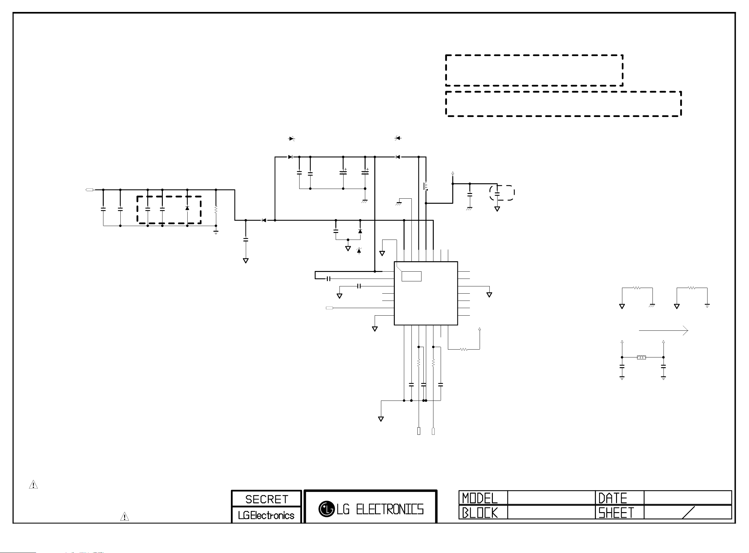
DVB-S2 LNB Part Allegro
Copyright ⓒ 2012 LG Electronics. Inc. All right reserved.
Only for training and service purposes
LGE Internal Use Only
DCDC_GND and A_GND are connected
DCDC_GND and A_GND are connected in pin#27
PCB_GND and A_GND are connected
(Option:LNB)
LNB_OUT
C6915
18pF
OPT
C6916
18pF
LNB
Close to Tuner
Surge protectioin
C6913
33pF
OPT
C6914
33pF
LNB
D6904
LNB
R6906
2.2K
1W
LNB
MBR230LSFT1G
C6900
0.22uF
LNB
25V
A_GND
2A
D6900
LNB
30V
D6901-*1
LNB_SX34
40V
D6901
LNB_SMAB34
40V
C6901
0.01uF
50V
LNB
C6912
C6902
1uF
68uF
50V
LNB
close to Boost pin(#1)
LNB_TX
35V
LNB
C6904
0.1uF
50V
LNB
C6903 0.1uF
LNB
A_GND
A_GND
C6905 22000pF
C6906
68uF
35V
LNB
DCDC_GND
LNB
D6902
LNB_SMAB34
40V
D6902-*1
LNB_SX34
40V
A_GND
A_GND
D6903-*1
LNB_SX34
LNB_SMAB34
BOOST
VCP
TCAP
NC_1
TDO
EXTM
TDI
40V
D6903
40V
DCDC_GND
LNB
[EP]
1
2
3
4
5
6
7
GND
28
THERMAL
8
3A
LNB
L6900
33UH
SP-7850_33
2.4A
BFI
VIN
GNDLX
24
25
26LX27
29
IC6900
A8290SETTR-T
LNB
9
10
SDA11ADD12SCL
VREG
LNB
R6901 33
R6900 33
LNB
OPT
C6907 0.22uF
C6908 27pF
Input trace widths should be sized to conduct at least 3A
Ouput trace widths should be sized to conduct at least 2A
+12V_LNB
A_GND
A_GND
C6911
0.1uF
50V
close to VIN pin(#25)
LNB
NC_9
23
13
NC_2
LNB
27pF
C6909
BFO
IRQ
OPT
C6910
10uF
25V
LNB
DCDC_GND
22
NC_8
21
NC_7
20
BFC
19
NC_6
18
NC_5
17
NC_4
16
NC_3
15
14
+3.3V_NORMAL
R6903
4.7K
LNB
R6904
0
A_GND
+12V
BLM18PG121SN1D
C6917
0.1uF
50V
LNB
L6901
LNB
DCDC_GND
Max 1.3A
+12V_LNB
A_GND
C6918
0.1uF
50V
LNB
R6905
0
THE SYMBOL MARK OF THIS SCHEMETIC DIAGRAM INCORPORATES
SPECIAL FEATURES IMPORTANT FOR PROTECTION FROM X-RADIATION.
FILRE AND ELECTRICAL SHOCK HAZARDS, WHEN SERVICING IF IS
ESSENTIAL THAT ONLY MANUFATURES SPECFIED PARTS BE USED FOR
THE CRITICAL COMPONENTS IN THE SYMBOL MARK OF THE SCHEMETIC.
A_GND
I2C_SDA4
I2C_SCL4
LNB
2011.11.21
69
Page 44
[51Pin LVDS Connector]
Copyright ⓒ 2012 LG Electronics. Inc. All right reserved.
Only for training and service purposes
LGE Internal Use Only
(For FHD FRC3 HS_LVDS)
P7200
FI-RE51S-HF-J-R1500
1
2
3
4
5
6
7
8
9
10
11
12
13
14
15
16
17
18
19
20
21
22
23
24
25
26
27
28
29
30
31
32
33
34
35
36
37
38
39
40
41
42
43
44
45
46
47
48
49
50
51
52
GND
NC
NC
NC
NC
NC
NC
LVDS_SEL
NC
NC
L/DIM_ENABLE
GND
RA0N
RA0P
RA1N
RA1P
RA2N
RA2P
GND
RACLKN
RACLKP
GND
RA3N
RA3P
RA4N
RA4P
GND
BIT_SEL
RB0N
RB0P
RB1N
RB1P
RB2N
RB2P
GND
RBCLKN
RBCLKP
GND
RB3N
RB3P
RB4N
RB4P
GND
GND
GND
GND
GND
NC
VLCD
VLCD
VLCD
VLCD
TP7204
TXA0N
TXA0P
TXA1N
TXA1P
TXA2N
TXA2P
TXACLKN
TXACLKP
TXA3N
TXA3P
TXA4N
TXA4P
TXB0N
TXB0P
TXB1N
TXB1P
TXB2N
TXB2P
TXBCLKN
TXBCLKP
TXB3N
TXB3P
TXB4N
TXB4P
L/DIM0_SCLK
L/DIM0_MOSI
L/DIM0_VS
I2C_BE_SDA1
I2C_BE_SCL1
FRC3_RESET
BPL_IN
LOCAL_DIM_EN
LOCAL_DIM_EN
PANEL_VCC
120-ohm
L7200
C7200
10uF
16V
OPT
C7201
1000pF
50V
OPT
C7202
0.1uF
16V
OPT
10K
R7200
R7201
0
FRC3_FLASH_WP
L/DIM0_SCLK
L/DIM0_MOSI
L/DIM0_VS
I2C_BE_SDA1
I2C_BE_SCL1
FRC3_RESET
THE SYMBOL MARK OF THIS SCHEMETIC DIAGRAM INCORPORATES
SPECIAL FEATURES IMPORTANT FOR PROTECTION FROM X-RADIATION.
FILRE AND ELECTRICAL SHOCK HAZARDS, WHEN SERVICING IF IS
ESSENTIAL THAT ONLY MANUFATURES SPECFIED PARTS BE USED FOR
THE CRITICAL COMPONENTS IN THE SYMBOL MARK OF THE SCHEMETIC.
LG1152 A0
Interface block
72 100
Page 45
LOCAL DIMMING
Copyright ⓒ 2012 LG Electronics. Inc. All right reserved.
Only for training and service purposes
LGE Internal Use Only
[To LED DRIVER]
P7600
12507WR-08L
L/DIM_OUT
1
2
3
4
5
6
7
8
9
+3.3V_NORMAL
R7600
10K
OPT
R7601
10K
L/DIM_OUT
AR7600
33
1/16W
L/DIM_OUT
R7606 33
L/DIM_OUT
R7607
4.7K
L/DIM_OUT
L/DIM0_SCLK
L/DIM0_MOSI
I2C_SCL1
I2C_SDA1
L/DIM0_VS
THE SYMBOL MARK OF THIS SCHEMETIC DIAGRAM INCORPORATES
SPECIAL FEATURES IMPORTANT FOR PROTECTION FROM X-RADIATION.
FILRE AND ELECTRICAL SHOCK HAZARDS, WHEN SERVICING IF IS
ESSENTIAL THAT ONLY MANUFATURES SPECFIED PARTS BE USED FOR
THE CRITICAL COMPONENTS IN THE SYMBOL MARK OF THE SCHEMETIC.
LOCAL DIMMING
2011.12.13
76
Page 46
eMMC I/F
Copyright ⓒ 2012 LG Electronics. Inc. All right reserved.
Only for training and service purposes
LGE Internal Use Only
EMMC_DATA[0-7]
EMMC_VCCQ
EMMC DATA LINE 47K PULL/UP
EMMC DATA LINE
10K PULL/UP
R8100 10K
R8101 10K
R8102 10K
R8103 10K
R8104 10K
R8105 10K
R8106 10K
C8107
10pF
50V
R8107 10K
DAT4
DAT3
R8100-*1 47K
R8102-*1 47K
R8101-*1 47K
EMMC_DATA[0]
EMMC_DATA[1]
EMMC_DATA[2]
EMMC_DATA[3]
EMMC_DATA[4]
EMMC_DATA[5]
EMMC_DATA[6]
EMMC_DATA[7]
EMMC_CLK
EMMC_CMD
EMMC_RST
R8103-*1 47K
R8104-*1 47K
R8105-*1 47K
R8106-*1 47K
R8107-*1 47K
AR8100
22
1/16W
AR8101
22
1/16W
AR8102 22
OPT
C8100
0.1uF
OPT
16V
Don’t Connect Power At VDDI
(Just Interal LDO Capacitor)
DAT5
DAT6
10K
R8117
EMMC_CLK_BALL
EMMC_CMD_BALL
10K
R8116
EMMC_RESET_BALL
EMMC_VCCQ
EMMC_VDDI
C8105
0.1uF
16V
EMMC_VDDI
C8106
2.2uF
10V
3.3V_EMMC
C8102
0.1uF
16V
DAT3
DAT4
DAT5
C8103
2.2uF
10V
C8104
0.1uF
16V
SDIN5D2-4G-974L1
A3
DAT0
A4
DAT1
A5
DAT2
B2
DAT3
B3
DAT4
B4
DAT5
B5
DAT6
B6
DAT7
M6
CLK
M5
CMD
A6
NC_3
A7
NC_4
C5
NC_23
E5
NC_42
E8
NC_43
E9
NC_44
E10
NC_45
F10
NC_52
G3
NC_58
G10
NC_59
H5
NC_66
J5
NC_73
K6
NC_80
K7
NC_81
K10
NC_82
P7
NC_116
P10
NC_119
K5
RESET
C6
VCCQ_1
M4
VCCQ_2
N4
VCCQ_3
P3
VCCQ_4
P5
VCCQ_5
E6
VCC_1
F5
VCC_2
J10
VCC_3
K9
VCC_4
C2
VDDI
E7
VSS_1
G5
VSS_2
H10
VSS_3
K8
VSS_4
C4
VSSQ_1
N2
VSSQ_2
N5
VSSQ_3
P4
VSSQ_4
P6
VSSQ_5
A1
NC_1
A2
NC_2
A8
NC_5
A9
NC_6
A10
NC_7
A11
NC_8
A12
NC_9
A13
NC_10
A14
NC_11
B1
NC_12
B7
NC_13
B8
NC_14
B9
NC_15
B10
NC_16
B11
NC_17
B12
NC_18
B13
NC_19
B14
NC_20
C1
NC_21
C3
NC_22
C7
NC_24
IC8100
C8
NC_25
C9
NC_26
C10
NC_27
C11
NC_28
C12
NC_29
C13
NC_30
C14
NC_31
D1
NC_32
D2
NC_33
D3
NC_34
D4
NC_35
D12
NC_36
D13
NC_37
D14
NC_38
E1
NC_39
E2
NC_40
E3
NC_41
E12
NC_46
E13
NC_47
E14
NC_48
F1
NC_49
F2
NC_50
F3
NC_51
F12
NC_53
F13
NC_54
F14
NC_55
G1
NC_56
G2
NC_57
G12
NC_60
G13
NC_61
G14
NC_62
H1
NC_63
H2
NC_64
H3
NC_65
H12
NC_67
H13
NC_68
H14
NC_69
J1
NC_70
J2
NC_71
J3
NC_72
J12
NC_74
J13
NC_75
J14
NC_76
K1
NC_77
K2
NC_78
K3
NC_79
K12
NC_83
K13
NC_84
K14
NC_85
L1
NC_86
L2
NC_87
L3
NC_88
NC_89
NC_90
NC_91
NC_92
NC_93
NC_94
NC_95
NC_96
NC_97
NC_98
NC_99
NC_100
NC_101
NC_102
NC_103
NC_104
NC_105
NC_106
NC_107
NC_108
NC_109
NC_110
NC_111
NC_112
NC_113
NC_114
NC_115
NC_117
NC_118
NC_120
NC_121
NC_122
NC_123
L12
L13
L14
M1
M2
M3
M7
M8
M9
M10
M11
M12
M13
M14
N1
N3
N6
N7
N8
N9
N10
N11
N12
N13
N14
P1
P2
P8
P9
P11
P12
P13
P14
SANDISK_EMMC_4GB
DAT5
DAT6
EMMC_RESET_BALL
EMMC_CMD_BALL
EMMC_CLK_BALL
A3
A4
A5
B2
B3
B4
B5
B6
M6
M5
A6
A7
C5
E5
E8
E9
E10
F10
G3
G10
H5
J5
K6
K7
K10
P7
P10
K5
C6
M4
N4
P3
P5
E6
F5
J10
K9
C2
E7
G5
H10
K8
C4
N2
N5
P4
P6
A1
A2
A8
A9
A10
A11
A12
A13
A14
B1
B7
B8
B9
B10
B11
B12
B13
B14
C1
C3
C7
IC8100-*3
H26M31001EFR
DAT0
DAT1
DAT2
DAT3
DAT4
DAT5
DAT6
DAT7
CLK
CMD
NC_3
NC_4
NC_23
NC_42
NC_43
NC_44
NC_45
NC_52
NC_58
NC_59
NC_66
NC_73
NC_80
NC_81
NC_82
NC_116
NC_119
RESET
VCCQ_1
VCCQ_2
VCCQ_3
VCCQ_4
VCCQ_5
VCC_1
VCC_2
VCC_3
VCC_4
VDDI
VSS_1
VSS_2
VSS_3
VSS_4
VSSQ_1
VSSQ_2
VSSQ_3
VSSQ_4
VSSQ_5
NC_1
NC_2
NC_5
NC_6
NC_7
NC_8
NC_9
NC_10
NC_11
NC_12
NC_13
NC_14
NC_15
NC_16
NC_17
NC_18
NC_19
NC_20
NC_21
NC_22
NC_24
C8
NC_25
C9
NC_26
C10
NC_27
C11
NC_28
C12
NC_29
C13
NC_30
C14
NC_31
D1
NC_32
D2
NC_33
D3
NC_34
D4
NC_35
D12
NC_36
D13
NC_37
D14
NC_38
E1
NC_39
E2
NC_40
E3
NC_41
E12
NC_46
E13
NC_47
E14
NC_48
F1
NC_49
F2
NC_50
F3
NC_51
F12
NC_53
F13
NC_54
F14
NC_55
G1
NC_56
G2
NC_57
G12
NC_60
G13
NC_61
G14
NC_62
H1
NC_63
H2
NC_64
H3
NC_65
H12
NC_67
H13
NC_68
H14
NC_69
J1
NC_70
J2
NC_71
J3
NC_72
J12
NC_74
J13
NC_75
J14
NC_76
K1
NC_77
K2
NC_78
K3
NC_79
K12
NC_83
K13
NC_84
K14
NC_85
L1
NC_86
L2
NC_87
L3
NC_88
L12
NC_89
L13
NC_90
L14
NC_91
M1
NC_92
M2
NC_93
M3
NC_94
NC_95
NC_96
NC_97
NC_98
NC_99
NC_100
NC_101
NC_102
NC_103
NC_104
NC_105
NC_106
NC_107
NC_108
NC_109
NC_110
NC_111
NC_112
NC_113
NC_114
NC_115
NC_117
NC_118
NC_120
NC_121
NC_122
NC_123
M7
M8
M9
M10
M11
M12
M13
M14
N1
N3
N6
N7
N8
N9
N10
N11
N12
N13
N14
P1
P2
P8
P9
P11
P12
P13
P14
DEV_HYNIX_EMMC_4GB
A3
A4
A5
B2
B3
B4
B5
B6
M6
M5
A6
A7
C5
E5
E8
E9
E10
F10
G3
G10
H5
J5
K6
K7
K10
P7
P10
K5
C6
M4
N4
P3
P5
E6
F5
J10
K9
C2
E7
G5
H10
K8
C4
N2
N5
P4
P6
A1
A2
A8
A9
A10
A11
A12
A13
A14
B1
B7
B8
B9
B10
B11
B12
B13
B14
C1
C3
C7
IC8100-*1
H26M21001ECR
DAT0
DAT1
DAT2
DAT3
DAT4
DAT5
DAT6
DAT7
CLK
CMD
NC_3
NC_4
NC_23
NC_42
NC_43
NC_44
NC_45
NC_52
NC_58
NC_59
NC_66
NC_73
NC_80
NC_81
NC_82
NC_116
NC_119
RESET
VCCQ_1
VCCQ_2
VCCQ_3
VCCQ_4
VCCQ_5
VCC_1
VCC_2
VCC_3
VCC_4
VDDI
VSS_1
VSS_2
VSS_3
VSS_4
VSSQ_1
VSSQ_2
VSSQ_3
VSSQ_4
VSSQ_5
NC_1
NC_2
NC_5
NC_6
NC_7
NC_8
NC_9
NC_10
NC_11
NC_12
NC_13
NC_14
NC_15
NC_16
NC_17
NC_18
NC_19
NC_20
NC_21
NC_22
NC_24
C8
NC_25
C9
NC_26
C10
NC_27
C11
NC_28
C12
NC_29
C13
NC_30
C14
NC_31
D1
NC_32
D2
NC_33
D3
NC_34
D4
NC_35
D12
NC_36
D13
NC_37
D14
NC_38
E1
NC_39
E2
NC_40
E3
NC_41
E12
NC_46
E13
NC_47
E14
NC_48
F1
NC_49
F2
NC_50
F3
NC_51
F12
NC_53
F13
NC_54
F14
NC_55
G1
NC_56
G2
NC_57
G12
NC_60
G13
NC_61
G14
NC_62
H1
NC_63
H2
NC_64
H3
NC_65
H12
NC_67
H13
NC_68
H14
NC_69
J1
NC_70
J2
NC_71
J3
NC_72
J12
NC_74
J13
NC_75
J14
NC_76
K1
NC_77
K2
NC_78
K3
NC_79
K12
NC_83
K13
NC_84
K14
NC_85
L1
NC_86
L2
NC_87
L3
NC_88
L12
NC_89
L13
NC_90
L14
NC_91
M1
NC_92
NC_93
NC_94
NC_95
NC_96
NC_97
NC_98
NC_99
NC_100
NC_101
NC_102
NC_103
NC_104
NC_105
NC_106
NC_107
NC_108
NC_109
NC_110
NC_111
NC_112
NC_113
NC_114
NC_115
NC_117
NC_118
NC_120
NC_121
NC_122
NC_123
M2
M3
M7
M8
M9
M10
M11
M12
M13
M14
N1
N3
N6
N7
N8
N9
N10
N11
N12
N13
N14
P1
P2
P8
P9
P11
P12
P13
P14
HYNIX_EMMC_2GB
KLM2G1HE3F-B001
A3
DAT0
A4
DAT1
A5
DAT2
B2
DAT3
B3
DAT4
B4
DAT5
B5
DAT6
B6
DAT7
M6
CLK
M5
CMD
A6
NC_3
A7
NC_4
C5
NC_23
E5
NC_42
E8
NC_43
E9
NC_44
E10
NC_45
F10
NC_52
G3
NC_58
G10
NC_59
H5
NC_66
J5
NC_73
K6
NC_80
K7
NC_81
K10
NC_82
P7
NC_116
P10
NC_119
K5
RSTN
C6
VDD_1
M4
VDD_2
N4
VDD_3
P3
VDD_4
P5
VDD_5
E6
VDDF_1
F5
VDDF_2
J10
VDDF_3
K9
VDDF_4
C2
VDDI
C4
VSS_1
E7
VSS_2
G5
VSS_3
H10
VSS_4
K8
VSS_5
N2
VSS_6
N5
VSS_7
P4
VSS_8
P6
VSS_9
A1
NC_1
A2
NC_2
A8
NC_5
A9
NC_6
A10
NC_7
A11
NC_8
A12
NC_9
A13
NC_10
A14
NC_11
B1
NC_12
B7
NC_13
B8
NC_14
B9
NC_15
B10
NC_16
B11
NC_17
B12
NC_18
B13
NC_19
B14
NC_20
C1
NC_21
C3
NC_22
C7
NC_24
IC8100-*2
C8
NC_25
C9
NC_26
C10
NC_27
C11
NC_28
C12
NC_29
C13
NC_30
C14
NC_31
D1
NC_32
D2
NC_33
D3
NC_34
D4
NC_35
D12
NC_36
D13
NC_37
D14
NC_38
E1
NC_39
E2
NC_40
E3
NC_41
E12
NC_46
E13
NC_47
E14
NC_48
F1
NC_49
F2
NC_50
F3
NC_51
F12
NC_53
F13
NC_54
F14
NC_55
G1
NC_56
G2
NC_57
G12
NC_60
G13
NC_61
G14
NC_62
H1
NC_63
H2
NC_64
H3
NC_65
H12
NC_67
H13
NC_68
H14
NC_69
J1
NC_70
J2
NC_71
J3
NC_72
J12
NC_74
J13
NC_75
J14
NC_76
K1
NC_77
K2
NC_78
K3
NC_79
K12
NC_83
K13
NC_84
K14
NC_85
L1
NC_86
L2
NC_87
L3
NC_88
L12
NC_89
L13
NC_90
L14
NC_91
SAMSUNG_EMMC_2GB
NC_92
NC_93
NC_94
NC_95
NC_96
NC_97
NC_98
NC_99
NC_100
NC_101
NC_102
NC_103
NC_104
NC_105
NC_106
NC_107
NC_108
NC_109
NC_110
NC_111
NC_112
NC_113
NC_114
NC_115
NC_117
NC_118
NC_120
NC_121
NC_122
NC_123
M1
M2
M3
M7
M8
M9
M10
M11
M12
M13
M14
N1
N3
N6
N7
N8
N9
N10
N11
N12
N13
N14
P1
P2
P8
P9
P11
P12
P13
P14
THE SYMBOL MARK OF THIS SCHEMETIC DIAGRAM INCORPORATES
SPECIAL FEATURES IMPORTANT FOR PROTECTION FROM X-RADIATION.
FILRE AND ELECTRICAL SHOCK HAZARDS, WHEN SERVICING IF IS
ESSENTIAL THAT ONLY MANUFATURES SPECFIED PARTS BE USED FOR
THE CRITICAL COMPONENTS IN THE SYMBOL MARK OF THE SCHEMETIC.
DU1
DUMMY_1
DU2
DUMMY_2
DU3
DUMMY_3
DU4
DUMMY_4
DU5
DUMMY_5
DU6
DUMMY_6
DU7
DUMMY_7
DU8
DUMMY_8
DUMMY_9
DUMMY_10
DUMMY_11
DUMMY_12
DUMMY_13
DUMMY_14
DUMMY_15
DUMMY_16
DU9
DU10
DU11
DU12
DU13
DU14
DU15
DU16
DU1
DUMMY_1
DU2
DUMMY_2
DU3
DUMMY_3
DU4
DUMMY_4
DU5
DUMMY_5
DU6
DUMMY_6
DU7
DUMMY_7
DU8
DUMMY_8
DUMMY_9
DUMMY_10
DUMMY_11
DUMMY_12
DUMMY_13
DUMMY_14
DUMMY_15
DUMMY_16
DU9
DU10
DU11
DU12
DU13
DU14
DU15
DU16
eMMC
11.09.29
81
Page 47
Place Near Micom
Copyright ⓒ 2012 LG Electronics. Inc. All right reserved.
Only for training and service purposes
LGE Internal Use Only
LOGO_LIGHT
+3.5V_ST
10K
R8902
R8901
10K
LOGO_LIGHT
OPT
C8900
0.1uF
16V
LOGO_LIGHT
1K
R8903
LOGO_LIGHT
LOGO_LIGHT
B
Q8900
MMBT3904(NXP)
+3.5V_ST
LOGO_LIGHT
R8910 33
LOGO_LIGHT
R8911 33
C
E
12507WR-03L
L8900
LOGO_LIGHT
BLM18PG121SN1D
P8900
1
LOGO_LIGHT
2
3
4
THE SYMBOL MARK OF THIS SCHEMETIC DIAGRAM INCORPORATES
SPECIAL FEATURES IMPORTANT FOR PROTECTION FROM X-RADIATION.
FILRE AND ELECTRICAL SHOCK HAZARDS, WHEN SERVICING IF IS
ESSENTIAL THAT ONLY MANUFATURES SPECFIED PARTS BE USED FOR
THE CRITICAL COMPONENTS IN THE SYMBOL MARK OF THE SCHEMETIC.
Page 48
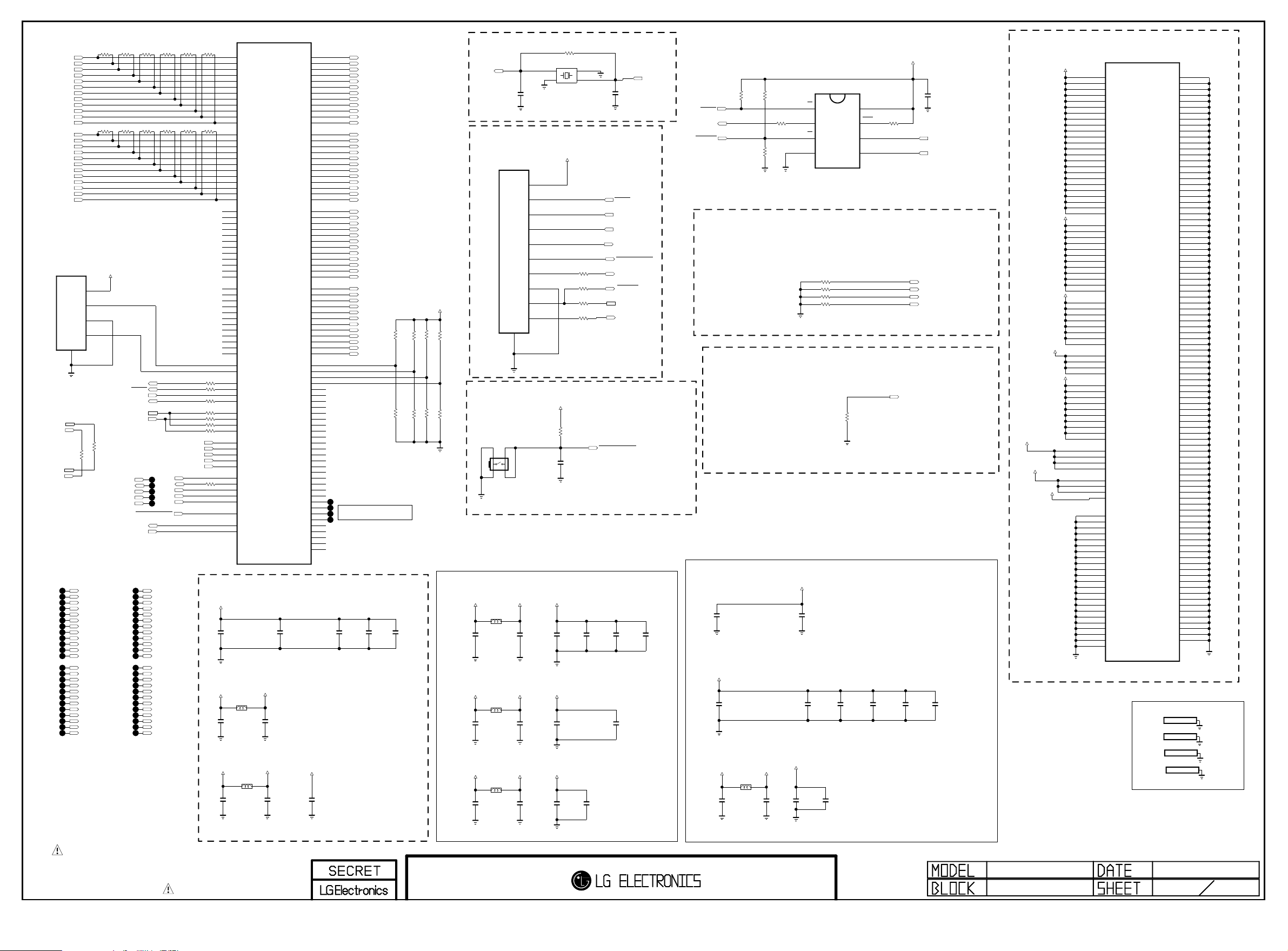
SOC_TXA0P
Copyright ⓒ 2012 LG Electronics. Inc. All right reserved.
Only for training and service purposes
LGE Internal Use Only
SOC_TXA0N
SOC_TXA1P
SOC_TXA1N
SOC_TXA2P
SOC_TXA2N
SOC_TXACLKP
SOC_TXACLKN
SOC_TXA3P
SOC_TXA3N
SOC_TXA4P
SOC_TXA4N
SOC_TXB0P
SOC_TXB0N
SOC_TXB1P
SOC_TXB1N
SOC_TXB2P
SOC_TXB2N
SOC_TXBCLKP
SOC_TXBCLKN
SOC_TXB3P
SOC_TXB3N
SOC_TXB4P
SOC_TXB4N
12507WS-04L
I2C_SDA2
I2C_SCL2
I2C_SDA1
I2C_SCL1
P9301
DEBUG
IC9300
LG1132
R9306
100
R9307
100
TRST_N
TXC0P
TXC0N
TXC1P
TXC1N
TXC2P
TXC2N
TXCCLKP
TXCCLKN
TXC3P
TXC3N
TXC4P
TXC4N
TXD0P
TXD0N
TXD1P
TXD1N
TXD2P
TXD2N
TXDCLKP
TXDCLKNTXBCLKN
TXD3P
TXD3N
TXD4P
TXD4N
R9308
R9310
100
100
AB17
RXA0P
AA17
RXA0N
Y16
RXA1P
Y17
RXA1N
AA16
RXA2P
AB16
RXA2N
AB15
RXACLKP
AA15
RXACLKN
Y14
RXA3P
Y15
RXA3N
AA14
RXA4P
AB14
AB13
AA13
AA12
AB12
AB11
AA11
AA10
AB10
AB21
AA21
RXA4N
RXB0P
RXB0N
Y12
RXB1P
Y13
RXB1N
RXB2P
RXB2N
RXBCLKP
RXBCLKN
Y10
RXB3P
Y11
RXB3N
RXB4P
RXB4N
AB9
RXC0P
AA9
RXC0N
Y8
RXC1P
Y9
RXC1N
AA8
RXC2P
AB8
RXC2N
AB7
RXCCLKP
AA7
RXCCLKN
Y6
RXC3P
Y7
RXC3N
AA6
RXC4P
AB6
RXC4N
AB5
RXD0P
AA5
RXD0N
Y4
RXD1P
Y5
RXD1N
AA4
RXD2P
AB4
RXD2N
AB3
RXDCLKP
AA3
RXDCLKN
Y2
RXD3P
Y3
RXD3N
AA2
RXD4P
AB2
RXD4N
D3
UART_RXD
D2
UART_TXD
C2
SPI_SCLK
C1
SPI_CS
B1
SPI_DI
B2
SPI_DO
E2
SDA_M
E1
SCL_M
D1
SDA_S
E3
SCL_S
F2
SMODE
F1
TMODE0
G3
TMODE1
G2
TMODE2
G1
TMODE3
H1
TRST_N
H3
TDO
H2
TDI
J3
TCK
J2
TMS
F3
PORES_N
XTALO
XTALI
R9311
R9309
100
100
R9312 33
R9313 33
R9314 33
R9315 33
R9316 33
R9317 33
R9318 33
SMODE
TMODE0
TMODE1
TMODE2
TMODE3
R9319 33
TDO
TDI
TCK
TMS
TXA0P
TXA0N
TXA1P
TXA1N
TXA2P
TXA2N
TXACLKP
TXACLKN
TXA3P
TXA3N
TXA4P
TXA4N
TXB0P
TXB0N
TXB1P
TXB1N
TXB2P
TXB2N
TXBCLKP
TXBCLKN
TXB3P
TXB3N
TXB4P
TXB4N
TXC0P
TXC0N
TXC1P
TXC1N
TXC2P
TXC2N
TXCCLKP
TXCCLKN
TXC3P
TXC3N
TXC4P
TXC4N
TXD0P
TXD0N
TXD1P
TXD1N
TXD2P
TXD2N
TXDCLKP
TXDCLKN
TXD3P
TXD3N
TXD4P
TXD4N
GPIO[0]
GPIO[1]
GPIO[2]
GPIO[3]
GPIO[4]
GPIO[5]
GPIO[6]
GPIO[7]
GPIO[8]
GPIO[9]
GPIO[10]
GPIO[11]
GPIO[12]
GPIO[13]
GPIO[14]
GPIO[15]
GPIO[16]
GPIO[17]
GPIO[18]
GPIO[19]
GPIO[20]
GPIO[21]
GPIO[22]
GPIO[23]
GPIO[24]
GPIO[25]
GPIO[26]
GPIO[27]
GPIO[28]
GPIO[29]
GPIO[30]
GPIO[31]
A10
B10
C9
C10
B9
A9
A8
B8
C7
C8
B7
A7
A6
B6
C5
C6
B5
A5
A4
B4
C3
C4
B3
A3
A18
B18
C17
C18
B17
A17
A16
B16
C15
C16
B15
A15
A14
B14
C13
C14
B13
A13
A12
B12
C11
C12
B11
A11
Y1
W3
W2
W1
V3
V2
V1
U3
U2
U1
T3
T2
T1
R3
R2
R1
P3
P2
P1
N3
N2
N1
M3
M2
M1
L1
L2
L3
K1
K2
K3
J1
TXA0P
TXA0N
TXA1P
TXA1N
TXA2P
TXA2N
TXACLKP
TXACLKN
TXA3P
TXA3N
TXA4P
TXA4N
TXB0P
TXB0N
TXB1P
TXB1N
TXB2P
TXB2N
TXBCLKP
TXBCLKN
TXB3P
TXB3N
TXB4P
TXB4N
TXC0P
TXC0N
TXC1P
TXC1N
TXC2P
TXC2N
TXCCLKP
TXCCLKN
TXC3P
TXC3N
TXC4P
TXC4N
TXD0P
TXD0N
TXD1P
TXD1N
TXD2P
TXD2N
TXDCLKP
TXDCLKN
TXD3P
TXD3N
OPT
TXD4P
TXD4N
Monitoring Pins for
3D-Depth Interanl status
R9320 10K
R9321 10K
NON_72INCH_LVDS_AB
OPT
R9322 10K
R9323 10K
+3.3V_NORMAL
OPT
OPT
R9324 10K
R9326 10K
R9325 10K
R9327 10K
+3.3V_IO Decaps
+3.3V_IO
C9300
0.1uF
16V
C9304
0.1uF
16V
OPT
OPT
C9308
0.1uF
16V
C9312
C9311
10uF
10uF
10V
10V
OPT
+3.3V Power Separation
C9301
4.7uF
10V
L9300
+3.3V_IO
C9303
4.7uF
10V
+3.3V_NORMAL
BLM18SG121TN1D
R9300
100
R9301
100
+3.3V_NORMAL
1
2
3
4
5
0
0
R9344
OPT
OPT
R9345
TXA0P
TXA0N
TXA1P
TXA1N
TXA2P
TXA2N
TXACLKP
TXACLKN
TXA3P
TXA3N
TXA4P
TXA4N
TXB0P
TXB0N
TXB1P
TXB1N
TXB2P
TXB2N
TXBCLKP
TXB3P
TXB3N
TXB4P
TXB4N
100
R9303
100
TRST_N
SPI_SCLK
I2C_SDA2
I2C_SCL2
TDO
TDI
TCK
TMS
XTAL_OUT
100
R9305
100
SPI_CS
SPI_DI
SPI_DO
3D_DEPTH_RESET
XTAL_IN
R9304
R9302
+3.3V XTAL AVDD Decaps
+3.3V_XTAL_AVDD
+3.3V_IO
BLM18SG121TN1D
C9307
4.7uF
10V
L9302
C9310
4.7uF
10V
+3.3V_XTAL_AVDD
C9314
0.1uF
16V
XTAL(24.75MHz)
XTAL_IN
C9333
30pF
50V
X-TAL_1
GND_1
R9329
1M
X9300
24.75MHz
1
2
4
3
GND_2
X-TAL_2
SPI/I2C For Aardvak Interface
P9300
12507WR-10L
DEBUG
11
LG1132 HW RESET
SW9300
JTP-1127WEM
12
DEBUG
4 3
+3.3V_NORMAL
1
2
3
4
5
6
OPT
+3.3V_NORMAL
OPT
R9330 0
R9331 0
DEBUG
R9332 0
OPT
R9333 0
OPT
R9328
10K
C9336
4.7uF
7
8
9
10
+2.5V LVDS_RX Decaps
+2.5V_LG1132
BLM18SG121TN1D
C9315
4.7uF
10V
+2.5V_LVDS_RX
L9303
C9318
4.7uF
10V
+2.5V_LVDS_RX
C9321
0.1uF
16V
C9324
0.1uF
16V
OPT
+2.5V LVDS_TX Decaps
+2.5V_LG1132
+2.5V_LG1132
+2.5V_LVDS_TX
L9304
BLM18SG121TN1D
C9316
4.7uF
10V
+2.5V DDR PLL/SS PLL/DIS PLL AVDD Decaps
+2.5V_AVDD
L9305
BLM18SG121TN1D
C9317
4.7uF
10V
C9319
4.7uF
10V
C9320
4.7uF
10V
+2.5V_LVDS_TX
C9322
0.1uF
16V
+2.5V_AVDD
C9323
0.1uF
16V
OPT
C9326
0.1uF
16V
OPT
C9339
30pF
50V
SPI_CS
SPI_DO
SPI_SCLK
SPI_DI
3D_DEPTH_RESET
TMODE0
FLASH_WP
I2C_SDA2
I2C_SCL2
3D_DEPTH_RESET
C9327
0.1uF
16V
C9328
0.1uF
16V
OPT
H8
VDD_1
H9
VDD_2
VDD_3
VDD_4
J8
VDD_5
VDD_6
K8
VDD_7
VDD_8
L8
VDD_9
VDD_10
M8
VDD_11
VDD_12
N8
VDD_13
VDD_14
P8
VDD_15
VDD_16
R8
VDD_17
R9
VDD_18
VDD_19
VDD_20
VDD_21
VDD_22
VDD_23
VDD_24
F4
VDD33_1
G4
VDD33_2
H4
VDD33_3
J4
VDD33_4
K4
VDD33_5
L4
VDD33_6
M4
VDD33_7
N4
VDD33_8
P4
VDD33_9
R4
VDD33_10
T4
VDD33_11
U4
VDD33_12
W7
LVRX_VDD25_1
W8
LVRX_VDD25_2
W9
LVRX_VDD25_3
LVRX_VDD25_4
LVRX_VDD25_5
LVRX_VDD25_6
LVRX_VDD25_7
LVRX_VDD25_8
LVTX_VDD10_1
LVTX_VDD10_2
LVTX_VDD10_3
LVTX_VDD10_4
D7
LVTX_VDD25_1
D8
LVTX_VDD25_2
D9
LVTX_VDD25_3
LVTX_VDD25_4
LVTX_VDD25_5
LVTX_VDD25_6
LVTX_VDD25_7
LVTX_VDD25_8
LVTX_VDD25_9
LVTX_VDD25_10
DISP_VDD
DR3P_VDD
SSP_VDD
XTAL_VDD
DISP_AVDD
DR3P_AVDD
SSP_AVDD
XTAL_AVDD
A2
VSS_1
VSS_2
VSS_3
VSS_4
D4
VSS_5
D5
VSS_6
D6
VSS_7
VSS_8
VSS_9
VSS_10
E4
VSS_11
E5
VSS_12
E6
VSS_13
E7
VSS_14
E8
VSS_15
E9
VSS_16
VSS_17
VSS_18
VSS_19
VSS_20
VSS_21
VSS_22
VSS_23
IC9300
LG1132
VSS_24
VSS_25
VSS_26
VSS_27
VSS_28
VSS_29
VSS_30
VSS_31
VSS_32
VSS_33
VSS_34
VSS_35
VSS_36
VSS_37
VSS_38
VSS_39
VSS_40
VSS_41
VSS_42
VSS_43
VSS_44
VSS_45
VSS_46
VSS_47
VSS_48
VSS_49
VSS_50
VSS_51
VSS_52
VSS_53
VSS_54
VSS_55
VSS_56
VSS_57
VSS_58
VSS_59
VSS_60
VSS_61
VSS_62
VSS_63
VSS_64
VSS_65
VSS_66
VSS_67
VSS_68
VSS_69
VSS_70
VSS_71
VSS_72
VSS_73
VSS_74
VSS_75
VSS_76
VSS_77
VSS_78
VSS_79
VSS_80
VSS_81
VSS_82
VSS_83
VSS_84
VSS_85
VSS_86
VSS_87
VSS_88
VSS_89
VSS_90
VSS_91
VSS_92
VSS_93
VSS_94
VSS_95
VSS_96
VSS_97
VSS_98
VSS_99
VSS_100
VSS_101
VSS_102
VSS_103
VSS_104
VSS_105
VSS_106
VSS_107
VSS_108
VSS_109
VSS_110
VSS_111
VSS_112
VSS_113
VSS_114
VSS_115
VSS_116
VSS_117
VSS_118
VSS_119
E17
E18
F5
F18
G5
G18
H5
H18
J5
J9
J10
J11
J12
J13
J14
J18
K5
K9
K10
K11
K12
K13
K14
K18
L5
L9
L10
L11
L12
L13
L14
L18
M5
M9
M10
M11
M12
M13
M14
M18
N5
N9
N10
N11
N12
N13
N14
N18
P5
P9
P10
P11
P12
P13
P14
P18
R5
R18
T5
T18
T19
U5
U18
U19
V4
V5
V6
V7
V8
V9
V10
V11
V12
V13
V14
V15
V16
V17
V18
V19
W4
W5
W6
W15
W16
W17
W18
W19
W20
W21
W22
Y18
Y19
AA1
AA18
AB18
SPI FLASH(4M Bit)
XTAL_OUT
R9334
R9335
4.7K
10K
R9336
100K
OPT
R9337
33
1/16W
SPI_CS
SPI_DI
FLASH_WP
TEST MODE Configuration
LG1132 Has Internal Pull-up
Default Setting
All ’H’ = Normal Operation Mode
TMODE[3:0]
0000 => System PLL Test
0001 => LVDS Rx Isolation Test
0010 => LVDS Tx Isolation Test
0011 => LVDS Bypass Test
0100 => ALL PLL Test
1001 => DDR PLL IsolationTest
1010 => Functional Test
1011 => MBIST
1100 => Scan Test(Normal)
1101 => Scan Test (Adaptive)
1110 => Display PLL Test
1111 => Normal Operation
DO[IO1]
GND
IC9301
W25X40BVSSIG
CS
1
2
WP
3
4
R9338 100
R9339 100
R9340 100
R9341 100
VCC
8
HOLD
7
CLK
6
DI[IO0]
5
LG1132_FLASH
OPT
OPT
OPT
OPT
System Configuration
Default Setting(’0’)
0 : Boot From Ext. Flash(Normal Booting)
1 : Internal RAM Boot (JTAG Booting)
R9342 100
+1.0V Power Separation
+1.0VDC
C9353
4.7uF
C9330
0.1uF
16V
OPT
10V
C9361
4.7uF
10V
+3.3V_NORMAL
R9343
3.3K
SMODE
TMODE0
TMODE1
TMODE2
TMODE3
C9365
0.1uF
SPI_SCLK
SPI_DO
+3.3V_IO
+2.5V_LVDS_RX
+2.5V_LVDS_TX
+1.0V_PLL_VDD
+2.5V_AVDD
+3.3V_XTAL_AVDD
+1.0VDC
+1.0VDC
AA22
AA19
AA20
AB20
AB19
H14
H15
J15
K15
L15
M15
N15
P15
R10
R11
R12
R13
R14
R15
W10
W11
W12
W13
W14
H10
H11
H12
H13
D10
D11
D12
D13
D14
D15
D16
Y21
Y22
Y20
A19
B19
C19
D17
D18
D19
E10
E11
E12
E13
E14
E15
E16
+1.0VDC Decaps
+1.0VDC
C9348
0.1uF
16V
OPT
+1.0V_XTAL/DDR3 PLL/SS PLL/DIS PLL_VDD
+1.0VDC
+1.0V_PLL_VDD
L9309
BLM18SG121TN1D
C9352
4.7uF
10V
C9357
4.7uF
10V
C9354
0.1uF
16V
OPT
+1.0V_PLL_VDD
C9359
0.1uF
16V
C9363
0.1uF
16V
C9356
10uF
10V
C9360
10uF
10V
C9364
0.1uF
16V
C9366
0.1uF
16V
OPT
OPT
M9300
MDS62110218
M9301
MDS62110218
M9302
MDS62110218
M9303
MDS62110218
ALBLOCK
ALBLOCK
ALBLOCK
ALBLOCK
For Heat Sink
THE SYMBOL MARK OF THIS SCHEMETIC DIAGRAM INCORPORATES
SPECIAL FEATURES IMPORTANT FOR PROTECTION FROM X-RADIATION.
FILRE AND ELECTRICAL SHOCK HAZARDS, WHEN SERVICING IF IS
ESSENTIAL THAT ONLY MANUFATURES SPECFIED PARTS BE USED FOR
THE CRITICAL COMPONENTS IN THE SYMBOL MARK OF THE SCHEMETIC.
LG1152 B0 2011. 11. 28
3D Depth
Page 49
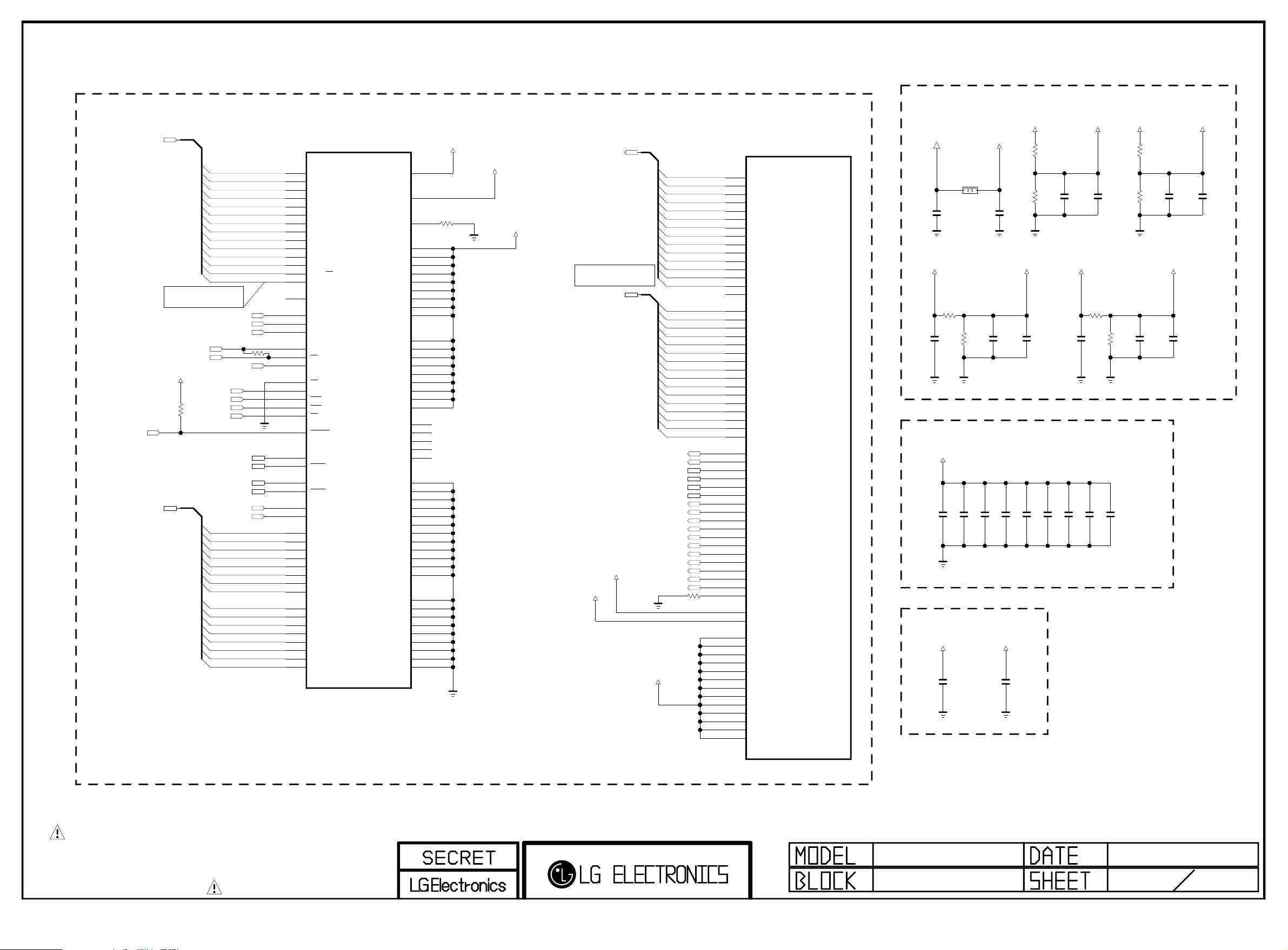
DDR0 PHY VREF
Copyright ⓒ 2012 LG Electronics. Inc. All right reserved.
Only for training and service purposes
LGE Internal Use Only
DDR_A[0-13]
DDR_RESET_N
DDR_DATA[0-15]
Connect A13 for
Using 2Gbit Memory
DDR_CLK
DDR_CLKN
+1.5VQ
DDR_ODT
R9400
200
DDR_RASN
DDR_CASN
DDR_WEN
DDR_A[0]
DDR_A[1]
DDR_A[2]
DDR_A[3]
DDR_A[4]
DDR_A[5]
DDR_A[6]
DDR_A[7]
DDR_A[8]
DDR_A[9]
DDR_A[10]
DDR_A[11]
DDR_A[12]
DDR_A[13]
DDR_BA[0]
DDR_BA[1]
DDR_BA[2]
R9401
DDR_CKE
DDR_DQS[0]
DDR_DQS_N[0]
DDR_DQS[1]
DDR_DQS_N[1]
DDR_DM[0]
DDR_DM[1]
DDR_DATA[0]
DDR_DATA[1]
DDR_DATA[2]
DDR_DATA[3]
DDR_DATA[4]
DDR_DATA[5]
DDR_DATA[6]
DDR_DATA[7]
DDR_DATA[8]
DDR_DATA[9]
DDR_DATA[10]
DDR_DATA[11]
DDR_DATA[12]
DDR_DATA[13]
DDR_DATA[14]
DDR_DATA[15]
100 1%
IC9400
H5TQ1G63DFR-PBC
N3
A0
P7
A1
P3
A2
N2
A3
P8
A4
P2
A5
R8
A6
R2
A7
T8
A8
R3
A9
L7
A10/AP
R7
A11
N7
A12/BC
T3
A13
M7
A15
M2
BA0
N8
BA1
M3
BA2
J7
CK
K7
CK
K9
CKE
L2
CS
K1
ODT
J3
RAS
K3
CAS
L3
WE
T2
RESET
F3
DQSL
G3
DQSL
C7
DQSU
B7
DQSU
E7
DML
D3
DMU
E3
DQL0
F7
DQL1
F2
DQL2
F8
DQL3
H3
DQL4
H8
DQL5
G2
DQL6
H7
DQL7
D7
DQU0
C3
DQU1
C8
DQU2
C2
DQU3
A7
DQU4
A2
DQU5
B8
DQU6
A3
DQU7
VREFCA
VREFDQ
VDD_1
VDD_2
VDD_3
VDD_4
VDD_5
VDD_6
VDD_7
VDD_8
VDD_9
VDDQ_1
VDDQ_2
VDDQ_3
VDDQ_4
VDDQ_5
VDDQ_6
VDDQ_7
VDDQ_8
VDDQ_9
NC_1
NC_2
NC_3
NC_4
NC_6
VSS_1
VSS_2
VSS_3
VSS_4
VSS_5
VSS_6
VSS_7
VSS_8
VSS_9
VSS_10
VSS_11
VSS_12
VSSQ_1
VSSQ_2
VSSQ_3
VSSQ_4
VSSQ_5
VSSQ_6
VSSQ_7
VSSQ_8
VSSQ_9
M8
H1
L8
ZQ
B2
D9
G7
K2
K8
N1
N9
R1
R9
A1
A8
C1
C9
D2
E9
F1
H2
H9
J1
J9
L1
L9
T7
A9
B3
E1
G8
J2
J8
M1
M9
P1
P9
T1
T9
B1
B9
D1
D8
E2
E8
F9
G1
G9
+0.75V_VREF_M0
R9402
240 1%
+0.75V_VREF_M1
+1.5VQ
DDR_A[0-13]
Connect A13 for
Using 2Gbit Memory
DDR_DATA[0-15]
+0.75V_VREF_D0
+0.75V_VREF_D1
DDR_A[0]
DDR_A[1]
DDR_A[2]
DDR_A[3]
DDR_A[4]
DDR_A[5]
DDR_A[6]
DDR_A[7]
DDR_A[8]
DDR_A[9]
DDR_A[10]
DDR_A[11]
DDR_A[12]
DDR_A[13]
DDR_DATA[0]
DDR_DATA[1]
DDR_DATA[2]
DDR_DATA[3]
DDR_DATA[4]
DDR_DATA[5]
DDR_DATA[6]
DDR_DATA[7]
DDR_DATA[8]
DDR_DATA[9]
DDR_DATA[10]
DDR_DATA[11]
DDR_DATA[12]
DDR_DATA[13]
DDR_DATA[14]
DDR_DATA[15]
DDR_CLK
DDR_CLKN
DDR_DQS[0]
DDR_DQS_N[0]
DDR_DQS[1]
DDR_DQS_N[1]
DDR_CKE
DDR_WEN
DDR_RASN
DDR_CASN
DDR_ODT
DDR_DM[0]
DDR_DM[1]
DDR_BA[0]
DDR_BA[1]
DDR_BA[2]
DDR_RESET_N
R9403 240
+1.5VQ
C9417
1000pF
R9409
1K
1%
+1.5VQ
R9410
1K
1%
R9411
1K
1%
+0.75V_VREF_D1
C9419
0.1uF
+0.75V_VREF_M1
C9421
1000pF
C9422
1000pF
C9420
0.1uF
R9406
1K
1%
R9407
1K
1%
C9410
C9412
OPT
+0.75V_VREF_M0
C9413
0.1uF
+1.5VQ
C9416
C9414
0.1uF
0.1uF
OPT
OPT
R9408
1K
1%
C9415
0.1uF
C9418
0.1uF
IC9300
LG1132
V21
DDR_A[0]
B22
DDR_A[1]
V20
DDR_A[2]
T20
DDR_A[3]
C22
DDR_A[4]
T21
DDR_A[5]
C21
DDR_A[6]
T22
DDR_A[7]
C20
DDR_A[8]
U22
DDR_A[9]
D22
DDR_A[10]
B21
DDR_A[11]
D20
DDR_A[12]
U21
DDR_A[13]
B20
DDR_A[14]
M22
DDR_DQ[0]
G20
DDR_DQ[1]
N20
DDR_DQ[2]
F22
DDR_DQ[3]
N22
DDR_DQ[4]
F20
DDR_DQ[5]
N21
DDR_DQ[6]
F21
DDR_DQ[7]
H21
DDR_DQ[8]
L22
DDR_DQ[9]
G22
DDR_DQ[10]
M20
DDR_DQ[11]
H22
DDR_DQ[12]
L21
DDR_DQ[13]
H20
DDR_DQ[14]
L20
DDR_DQ[15]
E22
DDR_CK
E21
DDR_CK_N
K22
DDR_DQS[0]
K21
DDR_DQS_N[0]
J22
DDR_DQS[1]
J21
DDR_DQS_N[1]
E20
DDR_CKE
R20
DDR_WE_N
P20
DDR_RAS_N
P21
DDR_CAS_N
P22
DDR_ODT
G21
DDR_DM[0]
M21
DDR_DM[1]
R21
DDR_BA[0]
D21
DDR_BA[1]
R22
DDR_BA[2]
U20
DDR_RST_N
A20
1%
V22
A21
E19
F19
G19
H19
J19
J20
K19
K20
L19
M19
N19
P19
R19
DDR_ZQ_CAL
DDR_VREF0
DDR_VREF1
DDR_VDDQ_1
DDR_VDDQ_2
DDR_VDDQ_3
DDR_VDDQ_4
DDR_VDDQ_5
DDR_VDDQ_6
DDR_VDDQ_7
DDR_VDDQ_8
DDR_VDDQ_9
DDR_VDDQ_10
DDR_VDDQ_11
DDR_VDDQ_12
DDR_VDDQ_13
+1.5V_LG1132
L9400
BLM18SG121TN1D
C9401
4.7uF
+1.5VQ
R9404
1K
1%
R9405
C9400
1K
0.1uF
1%
+1.5VQ
DDR3 1.5V Decaps - Place these caps near Memory
C9404
C9405
C9402
0.1uF
0.1uF
DDR3 1.5V/0.75V Decap
- Place these caps near IC101
+0.75V_VREF_D0
C9403
0.1uF
C9408
0.1uF
0.1uF
OPT
+0.75V_VREF_D1
C9409
0.1uF
+1.5VQ
+1.5VQ
C9407
4.7uF
+0.75V_VREF_D0
C9406
0.1uF
C9411
0.1uF
1000pF
0.1uF
THE SYMBOL MARK OF THIS SCHEMETIC DIAGRAM INCORPORATES
SPECIAL FEATURES IMPORTANT FOR PROTECTION FROM X-RADIATION.
FILRE AND ELECTRICAL SHOCK HAZARDS, WHEN SERVICING IF IS
ESSENTIAL THAT ONLY MANUFATURES SPECFIED PARTS BE USED FOR
THE CRITICAL COMPONENTS IN THE SYMBOL MARK OF THE SCHEMETIC.
LG1132 DDR3 2011. 06 .28
LG1132 DDR3
Page 50
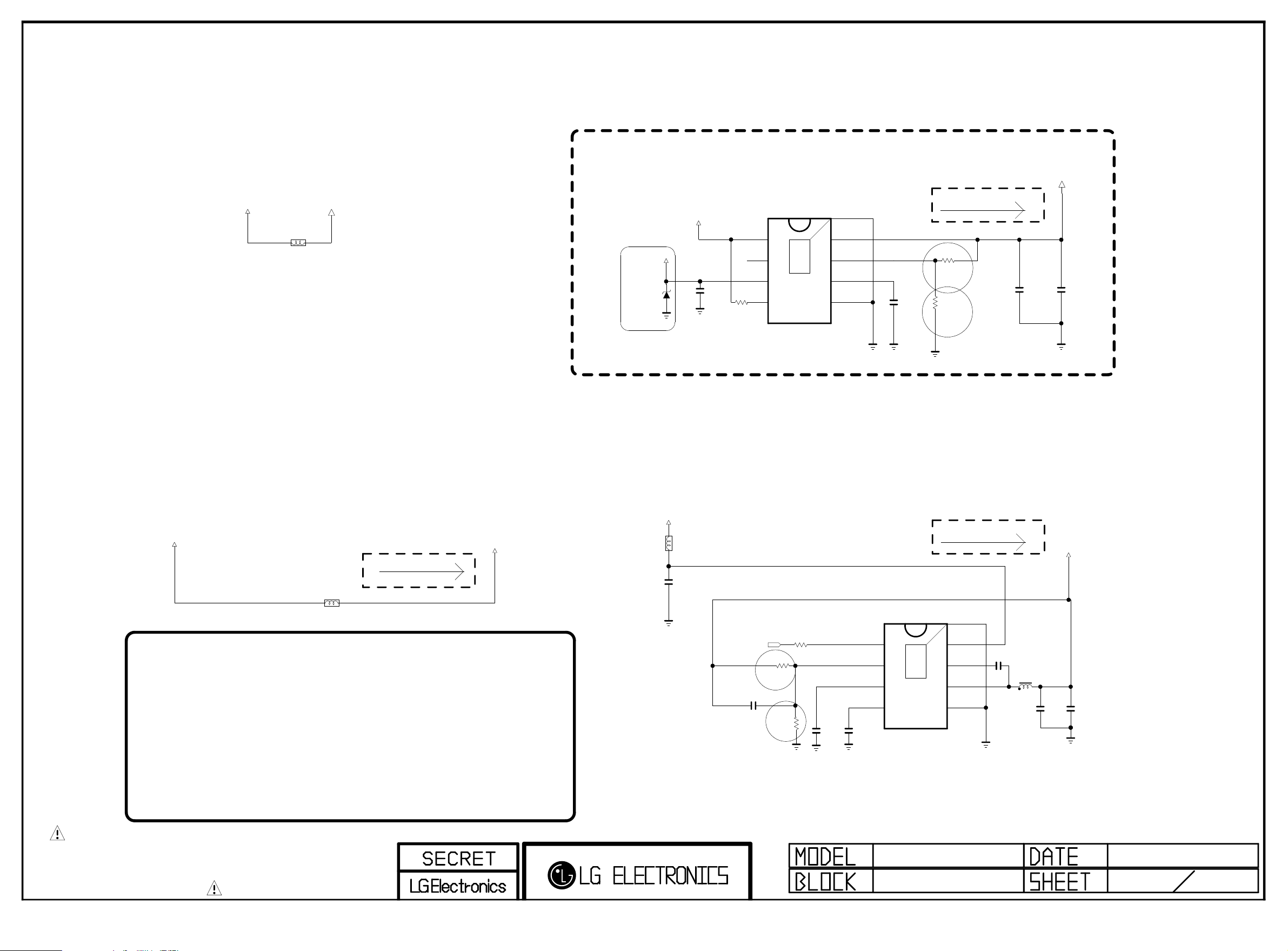
3D-Depth Analog for 2.5V
Copyright ⓒ 2012 LG Electronics. Inc. All right reserved.
Only for training and service purposes
LGE Internal Use Only
+1.5V_DDR
+1.5V_LG1132
L9500
BLM18PG121SN1D
+5V_USB
ZD9500
5.48VTO5.76V
Place near USB JACK
L9 CORE for 1.0V
+3.3V_NORMAL
C9500
10uF
10V
+2.5V
VCC
IN
PG
EN
IC9500
1
2
3
1.5A
4
9
THERMAL
[EP]
OUT
8
FB
7
SS
6
GND
5
AP7173-SPG-13 HF(DIODES)
R9500
10K
Vout=0.8*(1+R1/R2)
C9501
2200pF
50V
Max 600 mA
R9502
R1
4.3K
1%
R9501
2K
1%
R2
+2.5V_LG1132
C9513
10uF
10V
C9514
0.1uF
16V
LG1152 for 1.0V
+1.0VDC
+1.0VDC
**NON UD Model
LG1132 DDR = 668Mhz
LG1152 1.0V ==> IC2306
LG1132 1.0V ==> IC2306
**UD Model
LG1132 DDR = 792Mhz
LG1152 1.0V ==> IC2501
LG1132 1.1V ==> IC2306
NON_UD
CIC21J501NE
L9502
Max 2000 mA
+1.0V_VDD
(UD Model only / LG1132 DDR=792Mh)
+12V
UD
UD
Switching freq: 700K
READY
L9501
BLM18PG121SN1D
C9502
10uF
16V
POWER_ON/OFF2_3
R1
UD
R9503
C9503
100pF
50V
UD
R9505
R2
Max 2000 mA
IC9501
TPS54327DDAR
R9504
10K
11K
33K
1%
UD
C9504
UD
UD
1uF
10V
1%
UD
VREG5
C9505
3300pF
50V
VFB
EN
1
2
THERMAL
3
SS
4
3A
[EP]GND
VIN
8
VBST
9
7
UD
SW
6
GND
5
UD
Vout=0.765*(1+R1/R2)
16V
0.1uF
C9506
UD
L9503
3.6uH
UD
+1.0V_VDD
C9507
22uF
10V
OPT
C9508
22uF
10V
THE SYMBOL MARK OF THIS SCHEMETIC DIAGRAM INCORPORATES
SPECIAL FEATURES IMPORTANT FOR PROTECTION FROM X-RADIATION.
FILRE AND ELECTRICAL SHOCK HAZARDS, WHEN SERVICING IF IS
ESSENTIAL THAT ONLY MANUFATURES SPECFIED PARTS BE USED FOR
THE CRITICAL COMPONENTS IN THE SYMBOL MARK OF THE SCHEMETIC.
LG1132 Power 2011. 06. 28
LG1132 POWER
Page 51
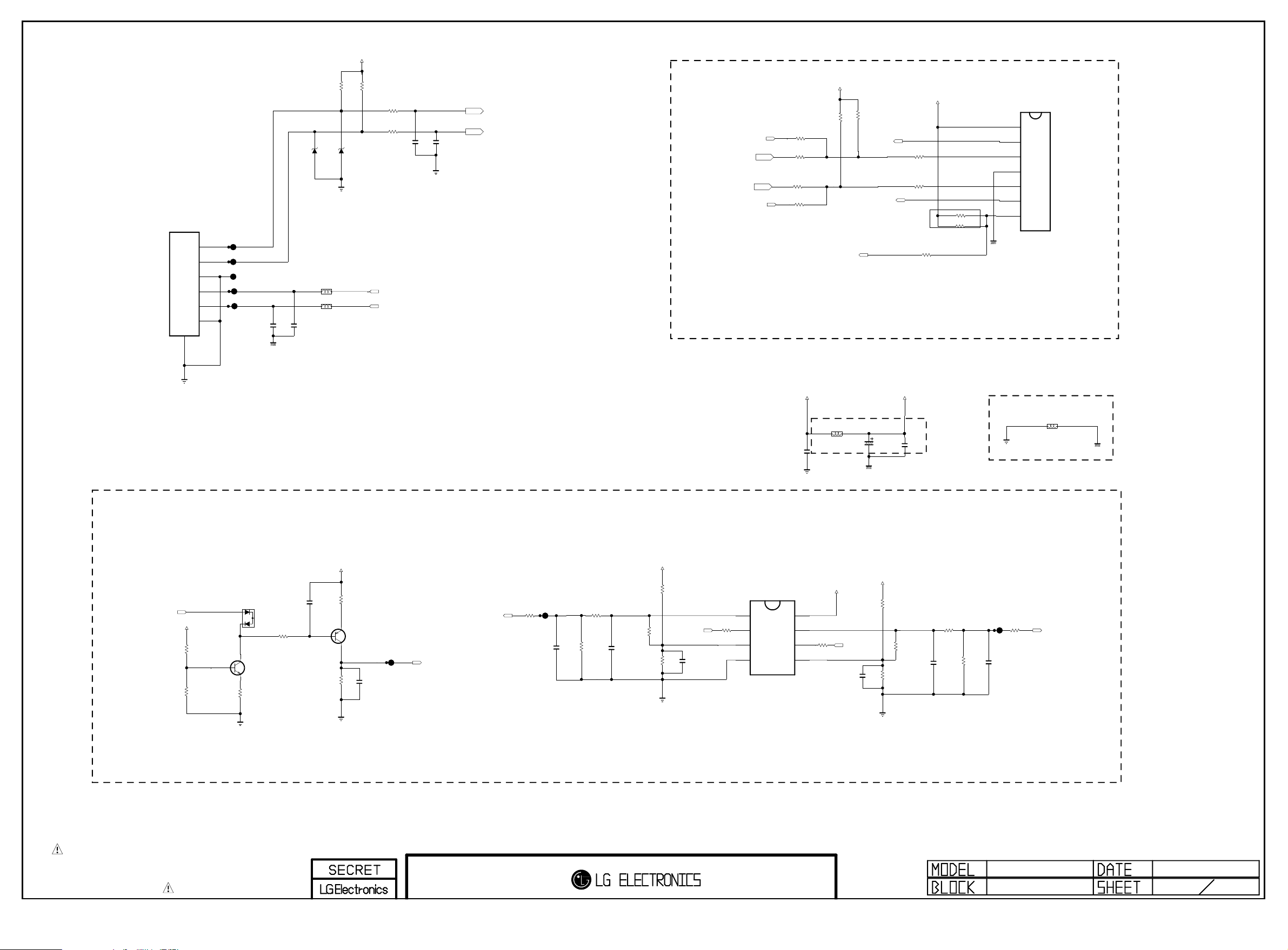
+3.3V_NORMAL
Copyright ⓒ 2012 LG Electronics. Inc. All right reserved.
Only for training and service purposes
LGE Internal Use Only
P10000
12507WR-06L
7
10K
10K
R10006
R10007
R10008
100
R10009
100
C10004
C10005
0.1uF
0.1uF
16V
ZD10000
8.2V
ZD10001
L10000
L10001
OPT
8.2V
UDZS8.2B
MOTOR-
MOTOR+
UDZS8.2B
1
2
3
4
5
6
JP10000
JP10001
JP10002
JP10003
JP10004
CLOSE
OPEN
MLB-201209-0120P-N2
MLB-201209-0120P-N2
C10000
0.1uF
50V
C10001
0.1uF
50V
OPT
16V
MOTOR_CLOSE_SW
MOTOR_OPEN_SW
L/DIM0_VS
MOTOR_CW
MOTOR_CCW
A_DIM
R10020
R10019
R10017
R10018
OPT
0
0
0
0
OPT
+12V
+3.3V_NORMAL
4.7K
4.7K
R10023
R10022
MOTOR+
SIGN100013
MOTOR-
MOTOR_SENSOR
MOTOR DRIVER
+12V_MOTOR
+12V_MOTOR
R10029
100
R10028
100
R10027
MOTOR_SENSOR
R10033
0
R10034
MOTOR_SENSOR
IC10001
BD6222HFP
VREF
1
OUT1
2
FIN
3
GND
4
RIN
5
OUT2
6
1
1
VCC
7
MAX 1500mA
C10009
0.1uF
50V
Close to IC7406
MLB-201209-0120P-N2
L10002
C10011
10uF
50V
C10012
0.1uF
50V
MLB-201209-0120P-N2
L10003
MOTOR Ground
+12V_MOTOR
MOTOR_SENSOR
+3.3V_NORMAL
R10001
22K
1/16W
MOTOR_SENSOR
R10000
18K
1/16W
MOTOR_SENSOR
MOTOR_SENSOR
D10000
BAT54SWT1
A
AC
C
1%
1%
C
Q10000
B
2SC3052
MOTOR_SENSOR
E
R100021K1/16W
MOTOR_SENSOR
1%
MOTOR_SENSOR
R10003
10K
1/16W
1%
MOTOR_SENSOR
C10002
0.1uF
25V
R100041K1/10W
E
B
Q10001
C
MMBT3906(NXP)
MOTOR_SENSOR
R10005
51K
1/8W
MOTOR_SENSOR
1%
MOTOR_SENSOR
C10003
0.1uF
1%
50V
MOTOR_SENSOR
JP10005
THE SYMBOL MARK OF THIS SCHEMETIC DIAGRAM INCORPORATES
SPECIAL FEATURES IMPORTANT FOR PROTECTION FROM X-RADIATION.
FILRE AND ELECTRICAL SHOCK HAZARDS, WHEN SERVICING IF IS
ESSENTIAL THAT ONLY MANUFATURES SPECFIED PARTS BE USED FOR
THE CRITICAL COMPONENTS IN THE SYMBOL MARK OF THE SCHEMETIC.
MO_SENS_TO_MAIN_DOWN
MOTOR_SENSOR_O
MOTOR_SENSOR
R10010
MOTOR_SENSOR
MOTOR_SENSOR
0
C10006
0.1uF
JP10006
50V
R10012
20K
10K
R10011
MOTOR_SENSOR
C10007
0.1uF
50V
MOTOR_SENSOR
MOTOR SENSOR OPTION
+12V_MOTOR
R10014
MOTOR_SENSOR
10K
OPT
R10013
R10015
MOTOR_SENSOR
22K
1/16W
1%
MOTOR_SENSOR_O
12K
1/10W
1%
C10008
0.1uF
50V
MOTOR_SENSOR
R10016
0
MOTOR_SENSOR
1
1
2
2
3
3
4
4
MOTOR_SENSOR
IC10000
KA4558D
8
8
7
7
6
6
MOTOR_SENSOR_UP
5
5
+12V_MOTOR
R10021
MOTOR_SENSOR_UP
0
MOTOR_SENSOR_O
C10010
0.1uF
50V
+12V_MOTOR
R10024
20K
1/16W
1%
MOTOR_SENSOR_UP
10K
R10025
22K
1/10W
1%
MOTOR_SENSOR_UP
OPT
R10026
C10013
0.1uF
50V
MOTOR_SENSOR_UP
R10030
20K
MOTOR_SENSOR_UP
10K
R10035
MOTOR_SENSOR_UP
JP10007
0
MOTOR_SENSOR_UP
C10014
0.1uF
50V
MOTOR_SENSOR_UP
MOTOR CONTROL
R10036
MO_SENS_TO_MAIN_UP
GP4
2011.07.01
Page 52
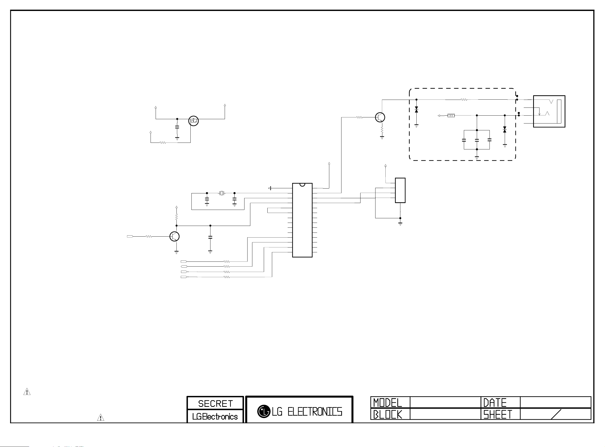
IR BLASTER
Copyright ⓒ 2012 LG Electronics. Inc. All right reserved.
Only for training and service purposes
LGE Internal Use Only
IR_B_RESET
+3.3V_NORMAL
+5V_NORMAL
R11001 1K
IR_Bla
IR_Bla
R11021
10K
+3.3V_IR_Bla
R11022
4.7K
IR_Bla
B
IRB_SPI_MOSI
IRB_SPI_MISO
IRB_SPI_SS
IRB_SPI_CK
IR_Bla
S
C11009
0.1uF
16V
OPT
C
Q11003
MMBT3904(NXP)
IR_Bla
E
G
D
AO3438
Q11002
IR_Bla
+3.3V_IR_Bla
IR_Bla
C11003
8MHz
22pF
X11001
50V
IR_Bla
C11010
0.1uF
16V
R11006
R11007
R11008
R11009
22
22
22
22
IR_Bla
IR_Bla
IR_Bla
IR_Bla
IR_Bla
C11005
22pF
50V
P20/RESETB
P10/KS8/MOSI1
P11/KS9/MISO1
P12/KS10/INT0
P13/KS11/INT1
P14/KS12/SS1/INT2
P15/KS13/XCK1/INT3
P16/KS14/MOSI0
P17/KS15/MISO0
P30/SS0/EC2/EXTREF
P31/XCK0/SENSOR
VSS
XIN
XOUT
IC11002
MC96FR3128R
1
IR_Bla
2
3
4
5
6
7
8
9
10
11
12
13
14
VDD
28
REMOUT
27
P22/INT3/DSDA
26
P21/INT2/DSCL
25
P07/KS7
24
P06/KS6
23
P05/KS5/EC3
22
P04/KS4/EC0
21
P03/KS3/T3/PWM3
20
P02/KS2/T2
19
P01/KS1/T1/PWM1
18
P00/KS0/T0
17
P37/INT1/SS0
16
P36/INT0/XCK0
15
+3.3V_IR_Bla
R11015 120
IR_Bla
Pattern Width : 0.5mm
C
B
IR_Bla
Q11001
SBT2222A_AUK
E
R11019
0
IR_Bla
IR_Bla
Close to JK11001
+3.3V_IR_Bla
P11001
12507WS-04L
1
IR_Bla
2
DSCL
3
DSDA
4
5
IR_B Micom Download
D11001
L11001
BLM18PG121SN1D
IR_Bla
+3.3V_IR_Bla
IR_Bla
R11020
10
IR_Bla
Pattern Width : 0.5mm
C11004
C11008
10uF
10uF
10V
IR_Bla
C11006
0.1uF
16V
OPT
IR_Bla
D11002
JP11002
JP11001
IR_Bla
1R
3DETECT
4L
5GND
KJA-PH-0-0177
JK11001
THE SYMBOL MARK OF THIS SCHEMETIC DIAGRAM INCORPORATES
SPECIAL FEATURES IMPORTANT FOR PROTECTION FROM X-RADIATION.
FILRE AND ELECTRICAL SHOCK HAZARDS, WHEN SERVICING IF IS
ESSENTIAL THAT ONLY MANUFATURES SPECFIED PARTS BE USED FOR
THE CRITICAL COMPONENTS IN THE SYMBOL MARK OF THE SCHEMETIC.
LG1152 A1 2011. 06. 02
IR Blaster/Boost
94
Page 53

Page 54

LCD TV Repair Guide
Copyright ⓒ 2012 LG Electronics. Inc. All right reserved.
Only for training and service purposes
LGE Internal Use Only
`12 years New Models
< Applicable Model >
XXLM9600-NA
Page 55

Overview for ’12 Broadband Model
Copyright ⓒ 2012 LG Electronics. Inc. All right reserved.
Only for training and service purposes
LGE Internal Use Only
Korea
(Hardware)
Page 56
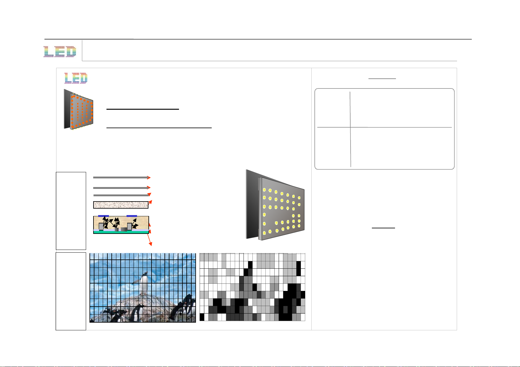
2 types of LED - ALEF
Copyright ⓒ 2012 LG Electronics. Inc. All right reserved.
Only for training and service purposes
LGE Internal Use Only
Benefit:MoreClearMoreReal
Feature
BLU
structure
ALEFType
LocalDimming
DBEF
Prism sheets
Diffuser plate
Light Blocking Pattern
Guiding Layer
Reflecting coating w/patterns
PCB
LED Array is on the back of Module
ALEFLED`
Local
Dimming
Bestpicturequality+thinTV
Slimmerdepth
betterpicturequality
Localdimmingdepictsmore
deepblack.
Model
XXLM9600
47inch : H(6) * V(4) = 24Block
55inch : H(6) * V(4) = 24Block
Local
Dimming
Page 57
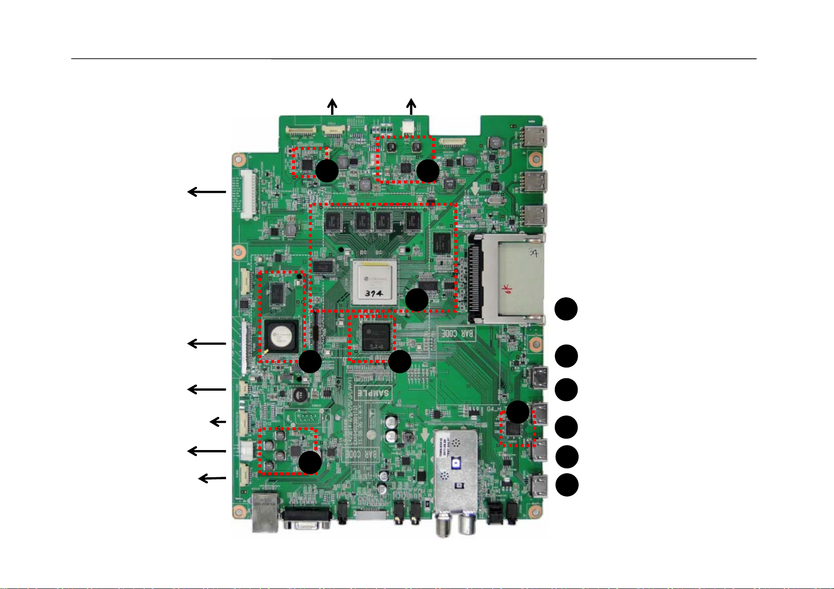
Main PCB for Broadband
Copyright ⓒ 2012 LG Electronics. Inc. All right reserved.
Only for training and service purposes
LGE Internal Use Only
Main + TCON all in one
XXLM9600-NA
To PSU
To FRC BOARD
Local Dim.
3
6
Woofer Spk
4
1
2
Main processor_Digital(LG1152D),
1
DDR Memory
Flash Memory
Main processor_analog(LG1152A)
2
wifi
Local Key +IR
Front Spk
Motion assy
Micom for Key/IR sensing
3
5
Audio AMP (10W+10W)
4
HDMI switch (4:1)
4
5
3D Depth Control IC,
6
DDR Memory
Page 58
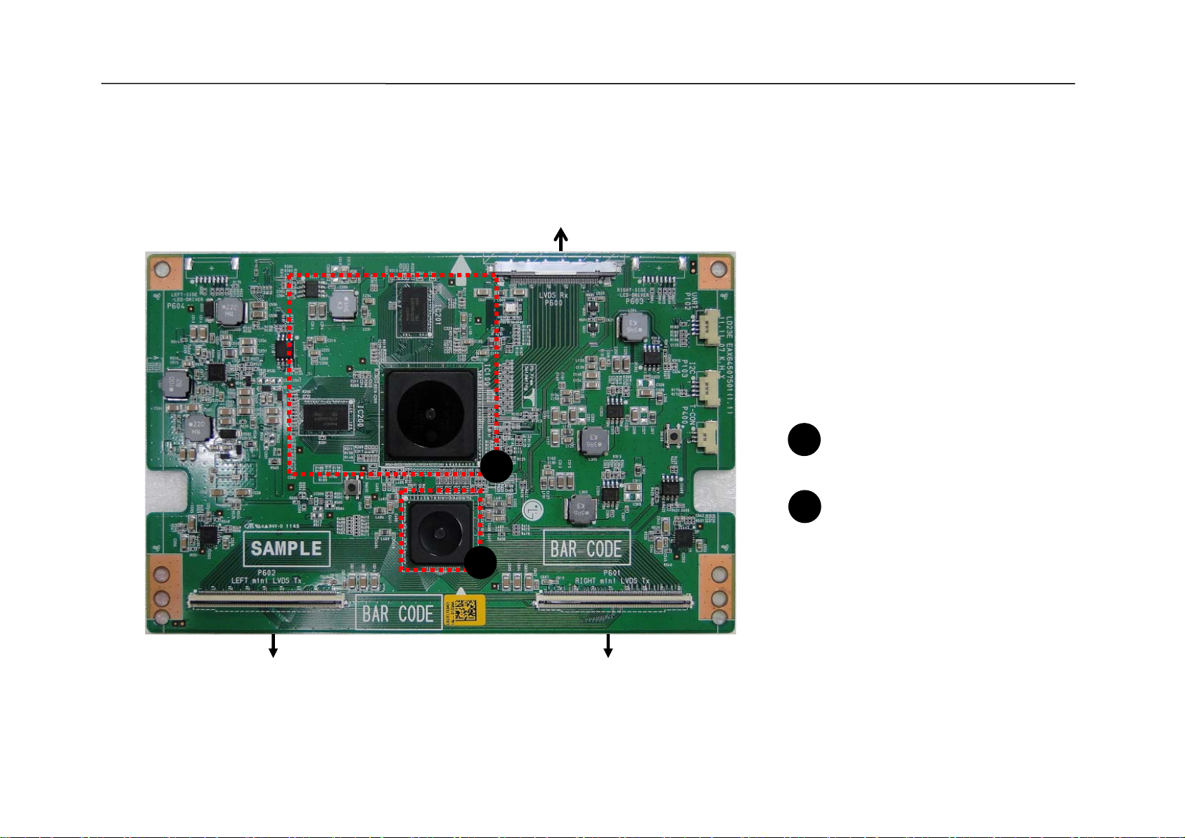
FRC Board for Broadband
Copyright ⓒ 2012 LG Electronics. Inc. All right reserved.
Only for training and service purposes
LGE Internal Use Only
XXLM9600-NA
From Main Board
1
Main + TCON all in one
FRC Processor(LG1122)
1
To Pannel ( Left )
T-Con IC(LG5812)
2
2
To Pannel ( Right )
Page 59
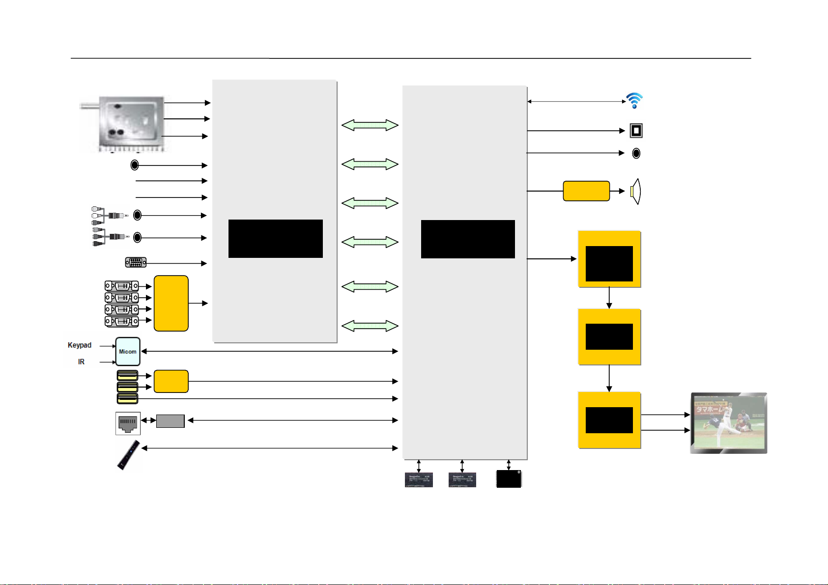
L9 Block diagram
Copyright ⓒ 2012 LG Electronics. Inc. All right reserved.
Only for training and service purposes
LGE Internal Use Only
Tuner
PC_AUDIO
A/V1
COMP1
PC-
RGB
HDMI1~4
USB1
USB2
USB3
LAN
DIF(P/N)
CVBS
SIF
PC_Audio L/R
AV 1_Audio L/R
Comp 1_Audio L/R
A/V1_CVBS
Comp1 Y,Pb,Pr
PC_R,G,B,H,V
HDMI
Switch
USB
HUB
PHY
RMII
L9
LG1152A
AUD
BB_TP_DATA
CHB_DATA
DAC_DATA
AAD_DATA
HSR_P/M
L9
LG1152D
SPDIF
H/P Audio L/R
I2S
HS_LVDS
2Link
Audio
AMP
3D
Depth
LG1132
HS_LVDS / 2Link
FRC-III
LG1122
V by One / 8 Line
T-con
LG5812
Built-in WiFi
OPTIC
H/P
SPK
mini_LVDS
mini_LVDS
Motion-R
M-Remote_R/TX
16
DDR
256MB×4
(1600)
16
DDR
128MB×1
(1600)
8
eMMC
4GB×1
Page 60
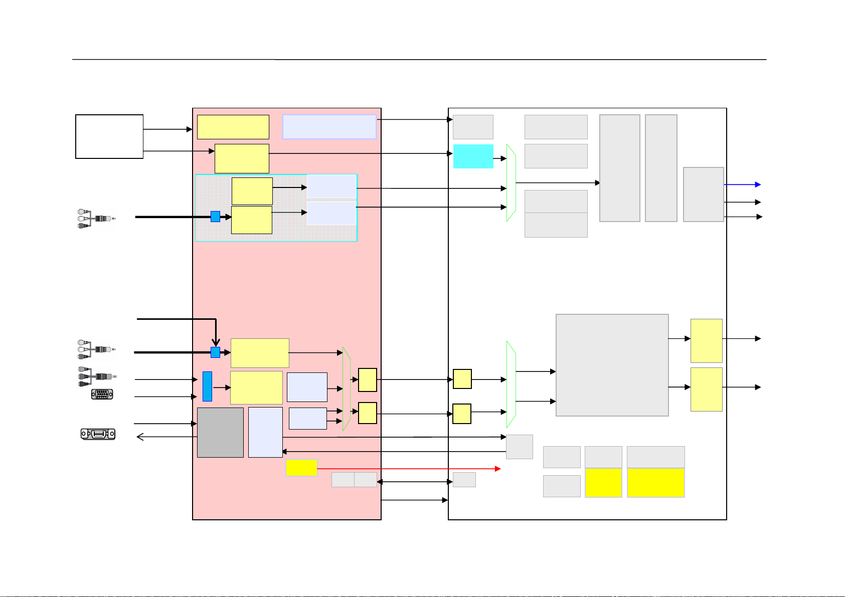
L9 Block diagram
Copyright ⓒ 2012 LG Electronics. Inc. All right reserved.
Only for training and service purposes
LGE Internal Use Only
ATSC Half NIM
DIF
SIF
Audio L/R (5-ch)
Tuner_CVBS
CVBS(6ch)
Component(2ch)
PC-RGB
HDMI(1ch)
ARC
(1ch)
GBB AFE
1ch@30MHz
w/ PLL
BTSC AFE
[email protected]
w/ PLL
1ch mono
Audio-ADC
24b@48KHz
1ch L/R
SW
Audio-ADC
24b@48KHz
CVBS AFE(2-ch)
SW
12b@54MHz
3ch Video
AFE
SW
10b@165MHz
w/ LLPLL
HDMI-Rx 1.4
(1-port PHY)
3D, ARC, 4kx2k
Analog Chip
Global Baseband
V/Q, DVB-T/C
Audio Codec0
(Digital Part)
Audio Codec1
(Digital Part)
12 : CVBS
Capture
Block
(3CH)
3D or UD
HDMI
(1-Link)
Data bridge
Audio PLL
w/ DCO
I2C
4(val, err, clk, sop)
+8 (data)
Parallel TS
System
Demux
10(data)+1(en)+5(gc)
3(lrck, lrch, sck)
I2S (mono)
I2S(stero)
3(lrck, lrch, sck)
12
LVDS
LVDS
I2C
12
I2S or SPDIF8
1 (ARC data)
Audio Clocks9
6(gbb, l9da)
interrupt
I2C
Mux
AAD
(THAT)
LVDS
LVDS
I2C
3(hdmi, 3ch, gbb)
Video Decoder
(Dual HD)
H.264 Encoder
SD upto 480p
CPU
Mux
Dual C-A9 (1GHz)
Graphic Engine
2D-VG / 3D Open-ES2.0
Video
Mux
Audio
Digital Chip
Audio
Diplay
Engine
MC NR,
Vertical MC IPC
Scaler, PE
OSD, VCR
Ethernet
MAC
eMMC
Controller
USB2.0
Host (x3)
PHY
(3-port)
Audio DSP
Multi-STD
Audio Decoder
DDR3(x16) * 3
DDR3-PHY
Sound
DSP
Digital
Audio
Output
LVDS
LVDS
(Headphone)
I2S
I2S
SPDIF
Video
OSD
Page 61
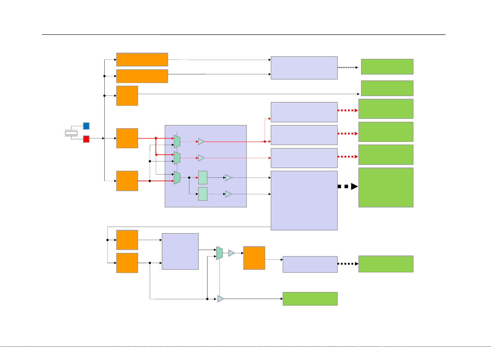
L9 Block diagram
Copyright ⓒ 2012 LG Electronics. Inc. All right reserved.
Only for training and service purposes
LGE Internal Use Only
xi_main
xo_main
24Mhz
2 port USB PHY
1 port USB PHY
DDR3PLL
DDR3PLL1
SSC setting
- 0xFD3001CC
- 0xFD3001D0
DDR3PLL2
SSC setting
- 0xFD3001C4
- 0xFD3001D8
SSC setting
- 0xFD3001D4
- 0xFD3001D8
1.6Ghz
1.6Ghz
30/48 Mhz
30/48Mhz
1 Ghz
CT
R
0 1 0 10 1
1/2
1/5
1.6Gh
z
1.6Ghz
800Mhz
800Mhz
i_m01_ddrclk
i_m2_ddrclk
i_core800_clk
i_core320_clk
dcoin_clk
Clock Divide & Reset generation
w/ test logic
u_crg
Clock Divide & Reset generation
w/ test logic
Clock Divide & Reset generation
w/ test logic
Clock Divide & Reset generation
w/ test logic
Clock Divide & Reset generation
w/ test logic
USB controller
CPU
Memory Controller
Memory Controller
Memory Controller
Video/Audio Block
CPU peripherial
200Mhz
200Mhz
About 220 internally generated clocks
DCO
DCO
de_dco_ou
t
27Mhz
sdec_dco_o
ut
27Mhz
Glitch-free logic
between
de_dco_out and
sdec_dco_out
CT
R
27Mhz
0 1
udnt_buf_dpll_fin
27Mhz
SSC setting
-0xFD300108
-0xFD30010C
DISPLL
u_DPLL
disp_fout
sclk
Clock Divide & Reset
generation w/ test logic
TE
DE
Page 62
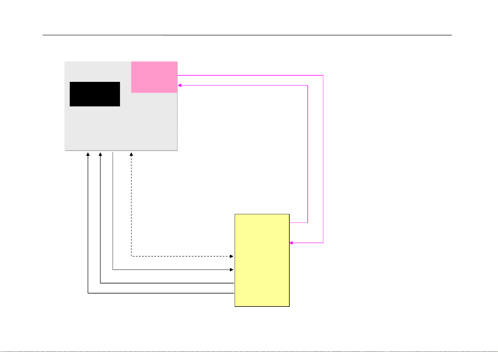
L9 Block diagram
Copyright ⓒ 2012 LG Electronics. Inc. All right reserved.
Only for training and service purposes
LGE Internal Use Only
Main SoC
L9
(B1)
SCL/DA6_3.3V
<ATSC>
IFAG
C
ADC_I_INN/P
IF_AGC
IF
N/P
I2CCH6(Main)
/TU_RESET
TU_SIF
TU_CVBS
ATSC H/NIM
Tuner
TDSS-H151F
Page 63
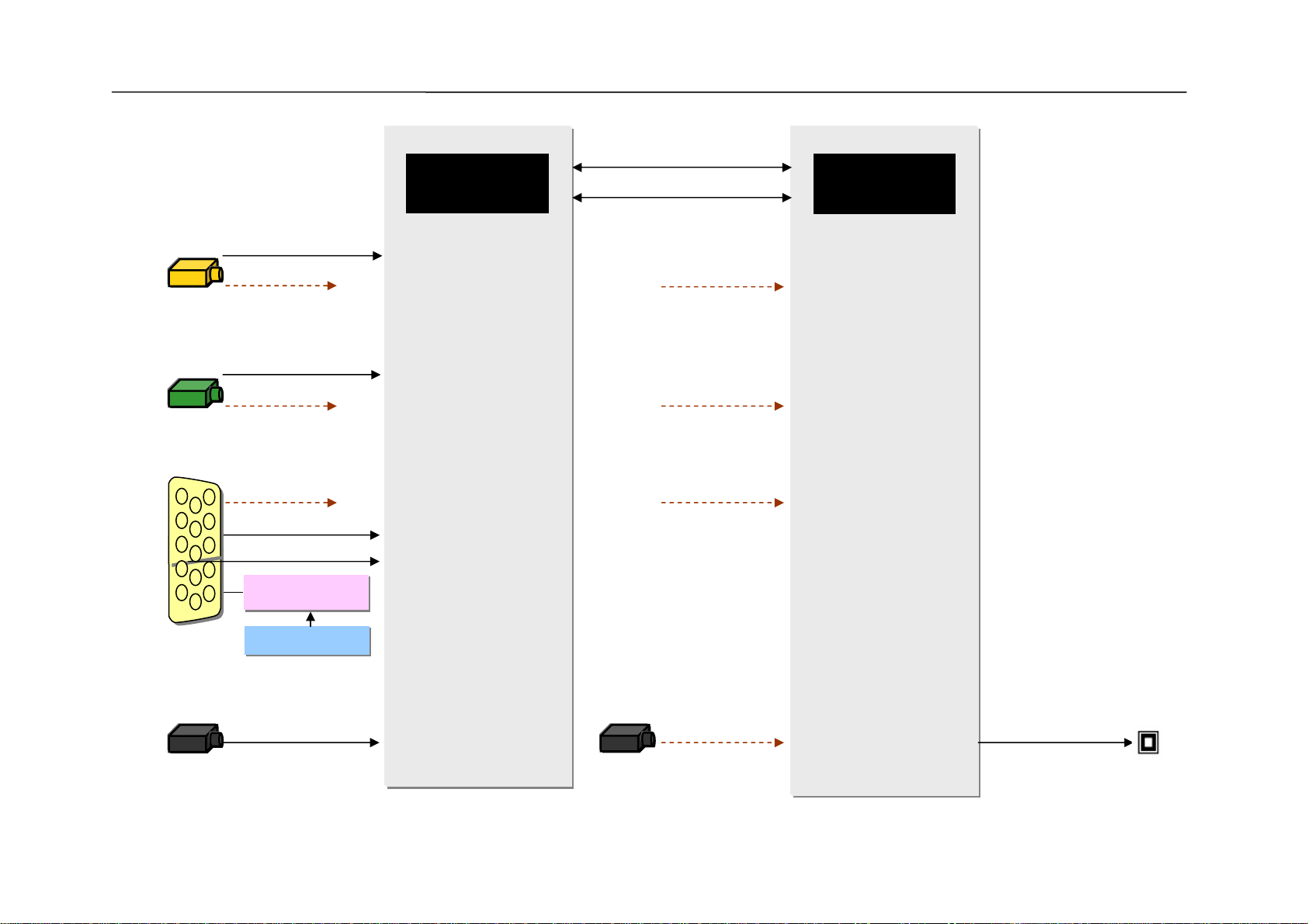
L9 Block diagram
Copyright ⓒ 2012 LG Electronics. Inc. All right reserved.
Only for training and service purposes
LGE Internal Use Only
L9
(LG1152A)
BB_TP/ CHB/ DAC/ AAD _DATA
HSR_P/M
L9
(LG1152D)
Phone JACK _Yellow
CVBS 1
Component 1
Phone JACK _Green
RGB
AV1_CVBS_IN
AV1_CVBS_DET
COMP1_Y/Pb/P
r
COMP1_DE
T
DSUB_DET
DSUB_R/ G/ B
DSUB_V/H SYNC
RGB_EDID
RGB_EDID
IC3600/ M24C02-RMN6T
IC3600/ M24C02-RMN6T
[EDID_WP] MICOM
[EDID_WP] MICOM
[CVBS_IN4]
[Y2/PB2/PR2_IN]
[R/G/B_IN]
[V/H SYNC]
AV1_CVBS_DET
COMP1_DE
T
DSUB_DET
[SPI_DI1/GPIO35]
[GPIO18]
[GPIO22]
PC AUDIO
PC_L/R_IN
[AUAD_L/R_CH5_IN]
EARPHONE
HP_DET
[GPIO4]
[IEC958OUT]
SPDIF_OUT
SPDIF
Page 64
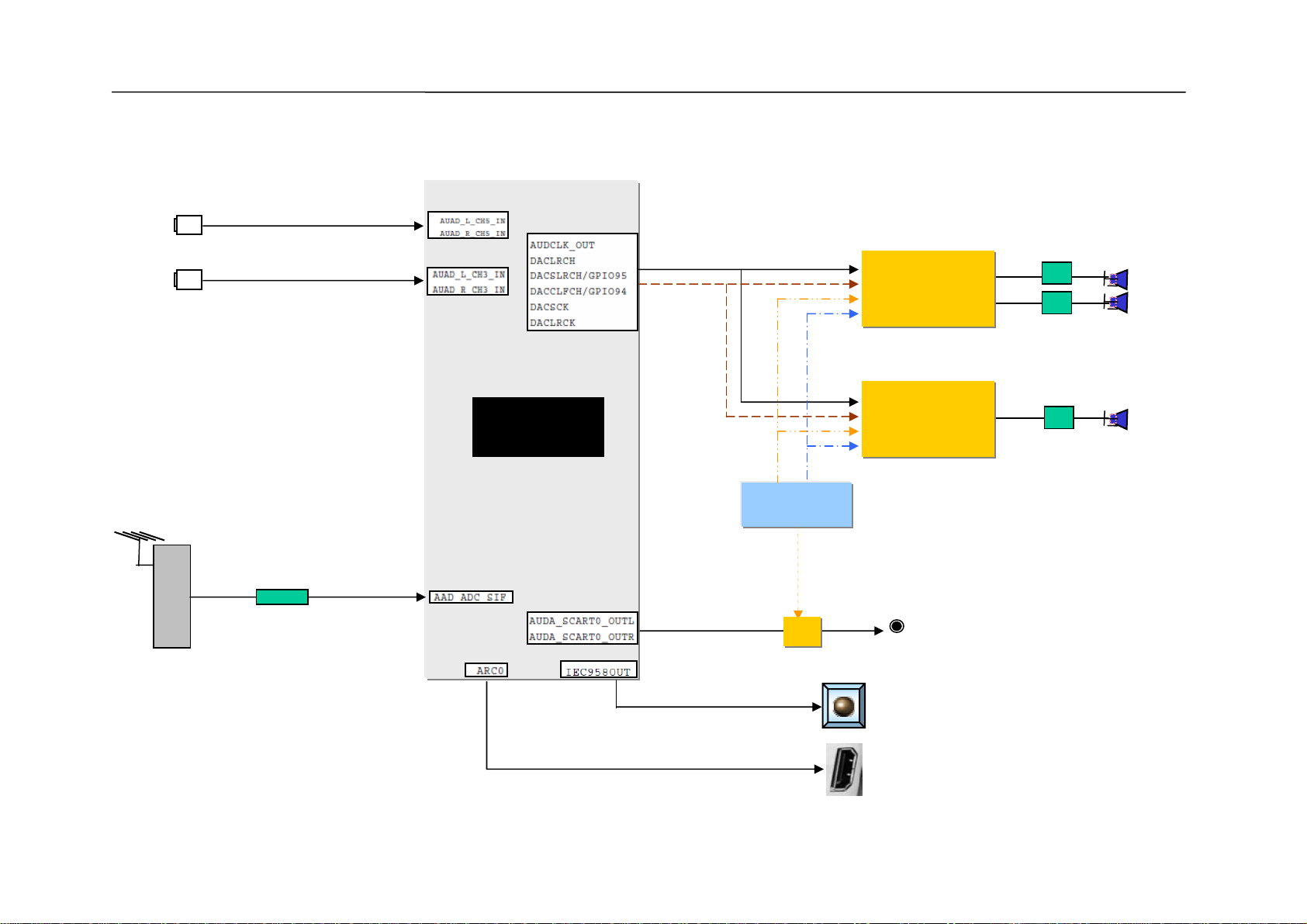
L9 Block diagram
Copyright ⓒ 2012 LG Electronics. Inc. All right reserved.
Only for training and service purposes
LGE Internal Use Only
PC_L/R_IN
MAIN
NTP7500
NTP7500
0x54
0x54
4P wafer
LPF
LPF
AV_L/R_IN
AUD_SCK/LRCK/LRCH
I2C2_SDA/SCL
WOOFER
L9
LG1152
AMP_MUTE
AMP_RESET
NTP7500
NTP7500
0x56
0x56
3P wafer / mon
LPF
MIC
SIDE_HP_MUTE
OM
TR BUF
Tuner
TU_SIF
HP_LOUT/ROUT
SPDIF_OUT
TPA
TPA
6132
6132
HEAD PHONE
SPDIF_OUT_ARC
HDMI1
HDMI1
Page 65
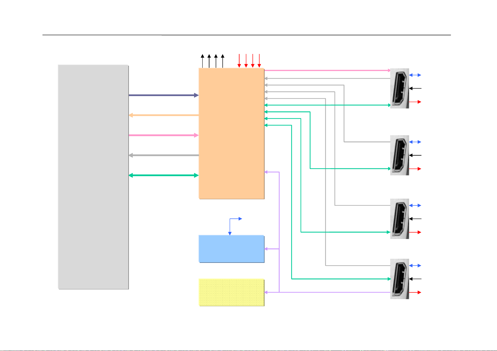
L9 Block diagram
Copyright ⓒ 2012 LG Electronics. Inc. All right reserved.
Only for training and service purposes
LGE Internal Use Only
HDMI_HPD_1 ~ 4 5V_HDMI_1 ~ 4
L9_B1
Main SoC
(IC100 /
LG1152D-B1)
HDMI_S/W_RESE
T
HDMI_INT
SPDIF_OUT_AR
C
HDMI Out put 8bits
I2C_SCL/SDA 5 2bits
SPDIF_OUT_AR
C
HDMI
Switch
(IC3201 / SII9587CNUC)
CEC_REMOTE
MICOM
TMDS Link
8bits
DDC_I2C 2bits
TMDS Link
8bits
DDC_I2C 2bits
TMDS Link
8bits
DDC_I2C 2bits
HDM
HDM
I1
I1
HDM
HDM
I2
I2
HDM
HDM
I3
I3
CEC_REMOTE
HDMI_HPD_1
5V_HDMI_1
CEC_REMOTE
HDMI_HPD_2
5V_HDMI_2
CEC_REMOTE
HDMI_HPD_3
5V_HDMI_3
(IC3000 /
R5F100GEAFB)
Power Switch
(IC3202 /
TPS2554)
TMDS Link
8bits
DDC_I2C 2bits
MHL_DET
HDM
HDM
I4
I4
CEC_REMOTE
HDMI_HPD_4
5V_HDMI_4
Page 66
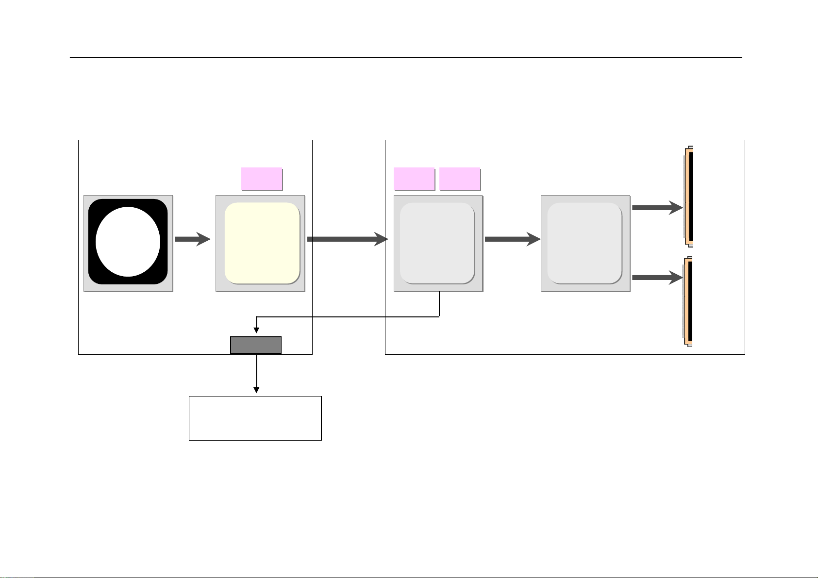
240Hz Backend Block diagram
Copyright ⓒ 2012 LG Electronics. Inc. All right reserved.
Only for training and service purposes
LGE Internal Use Only
Main Board T-Con Board
DDR3@
DDR3@
800MHz
800MHz
L9D
(LG1152)
2 link
HS-LVDS
3D Chip
3D Chip
(LG1132)
(LG1132)
2 link
HS-LVDS
51P Cable
51P Cable
DDR3@
DDR3@
800MHz
800MHz
FRC-III
FRC-III
(LG1122)
(LG1122)
DDR3@
DDR3@
800MHz
800MHz
8 lanes
VbyOne
T-Con
T-Con
(LG5812)
(LG5812)
Mini-LVDS
Mini-LVDS
80Pin
Mini -LVDS
Output
80Pin
Mini -LVDS
Output
8P L/Dimming
LED Driver
Page 67
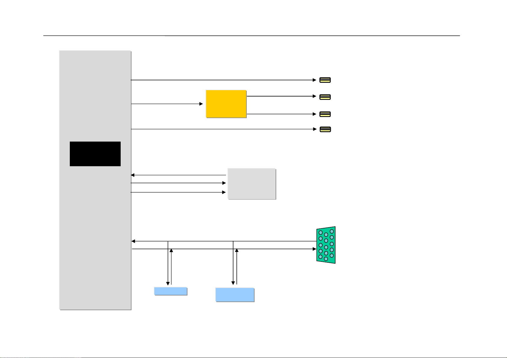
L9 Block diagram
Copyright ⓒ 2012 LG Electronics. Inc. All right reserved.
Only for training and service purposes
LGE Internal Use Only
L9
(B1)
[M_REMOTE_RESET/ISP]
[UART0_RX / GPIO49]
[UART0_TX / GPIO50]
[USB_DM2 / DP2]
[USB_DM1 / DP1]
[BT_USB_DP/DM]
[UART2_RX]
[UART2_TX]
USB DM3 /
DP3
USB_HUB_IC_IN_DP /
DM
WIFI_DM / DP
M_REMOTE_RX
M_REMOTE_TX
M_REMOTE_RESET/ISP
SOC_RX
SOC_TX
USB HUB
USB_DM2 / DP2
USB_DM1 / DP1
Motion Remote
Receiver
USB3
USB2
USB1
DVR Ready
USB WIFI
SOC_RX
MICOM
SOC_TX
SOC_RX
SOC_TX
4Pin debugging
Wafer
P3800
15Pin RGB PC
Page 68
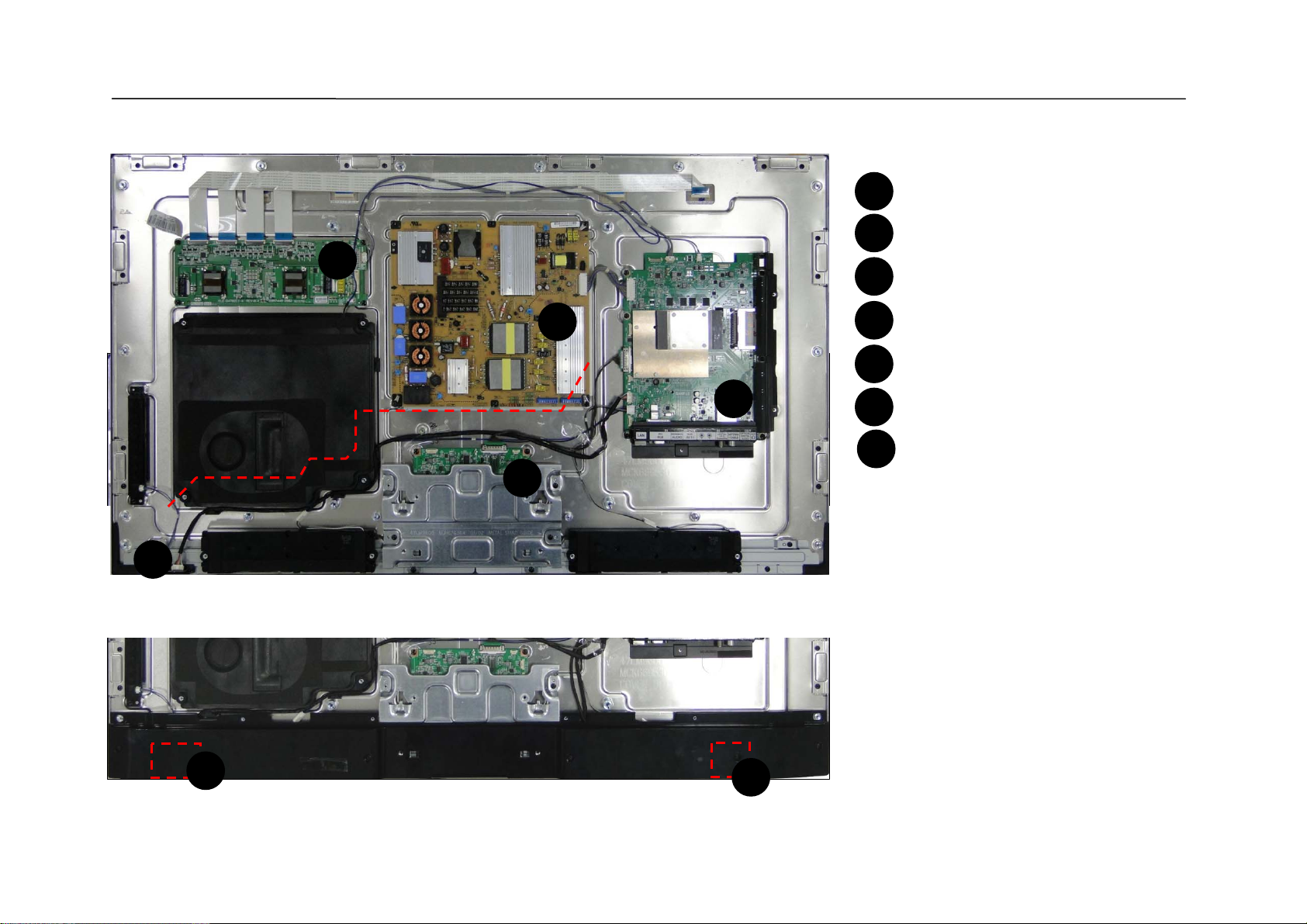
Interconnection - 1
Copyright ⓒ 2012 LG Electronics. Inc. All right reserved.
Only for training and service purposes
LGE Internal Use Only
2
[PCBs]XXLM9600-NA
1
Main PCB
2
LED driver
3
WIFI ASSY
4
7
RF MOTION ASSY
5
1
6
5
4
3
6
FRC ASSY
7
IR Key PCB
PSU
Page 69
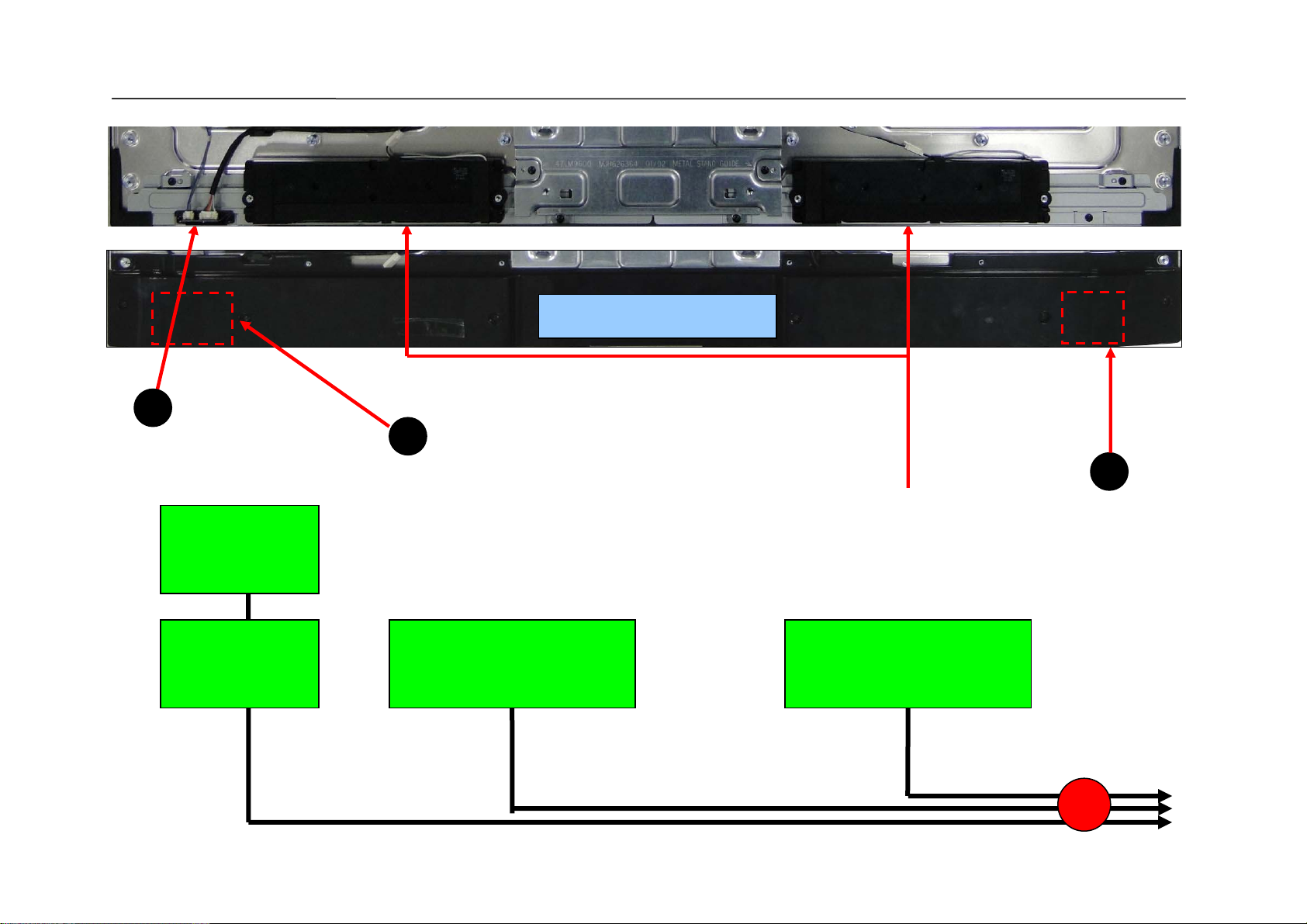
Interconnection – sub PCB( XXLM9600 Series )
Copyright ⓒ 2012 LG Electronics. Inc. All right reserved.
Only for training and service purposes
LGE Internal Use Only
Speaker cover Assy
5
IR Key PCB
RF MOTION ASSY
4
3
Local Key
PCB
IR PCB WIFI ASSY
RF MOTION ASSY
SPK unit
WIFI ASSY
1
To Main
Page 70
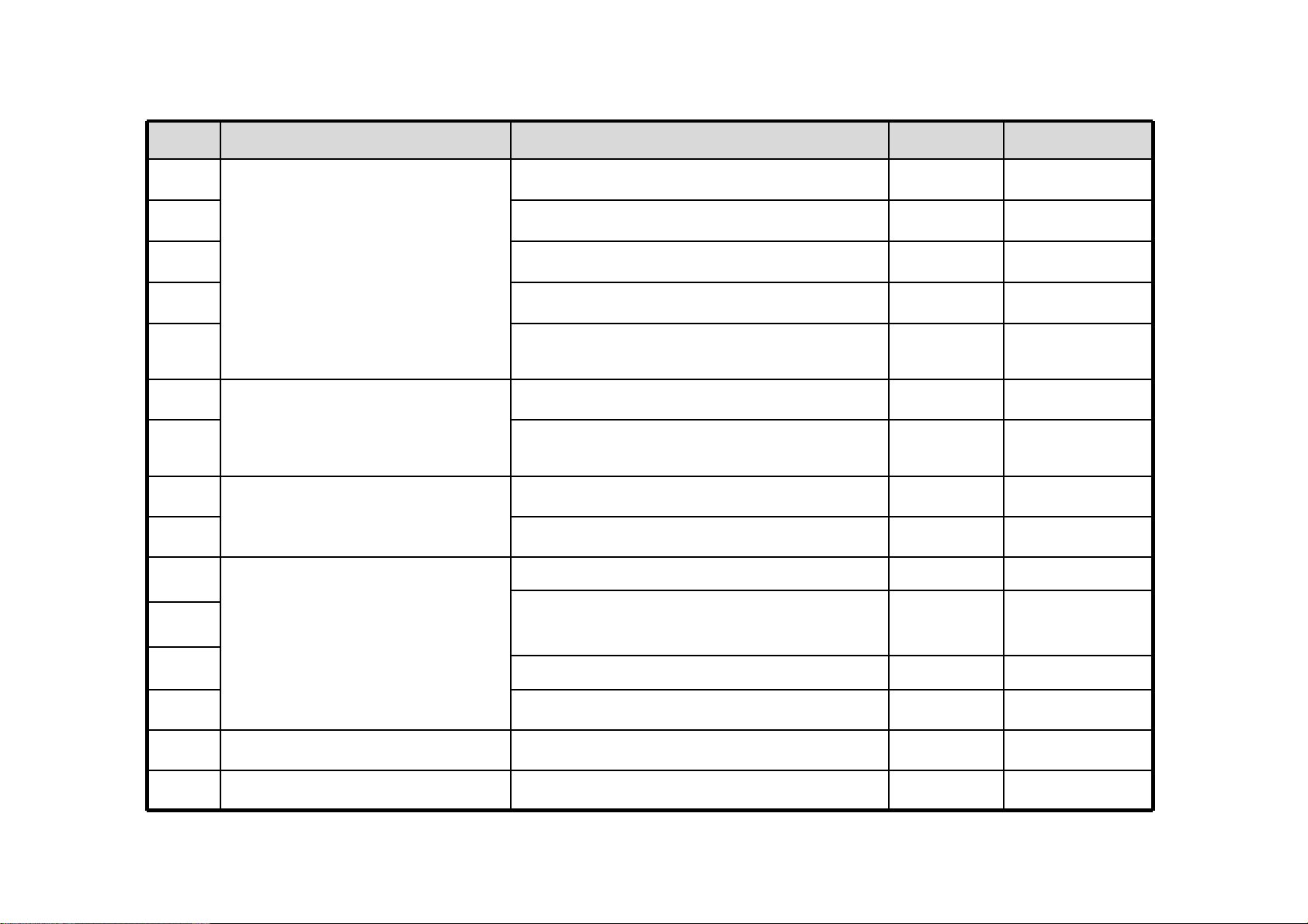
Contents of LCD TV Standard Repair Process
Copyright ⓒ 2012 LG Electronics. Inc. All right reserved.
Only for training and service purposes
LGE Internal Use Only
No.
1
2 No video/No audio 2
3 Picture broken/ Freezing 3
4 Color error 4
5
6
7
8
9 Wrecked audio/discontinuation/noise 9
10
Error symptom (High
category)
A. Video error
B. Power error
C. Audio error
Error symptom (Mid category) Page Remarks
No video/Normal audio 1
Vertical/Horizontal bar, residual image,
light spot, external device color error
No power 6
Off when on, off while viewing, power
auto on/off
No audio/Normal video 8
Remote control & Local switch checking 10
5
7
11
D. Function error
12
13 External device recognition error 13
14 E. Noise Circuit noise, mechanical noise 14
15 F. Exterior error Exterior defect 15
First of all, Check whether there is SVC Bulletin in GCSC System for these model.
M4 operating checking 11
Wifi operating checking 12
Page 71
Standard Repair Process
Copyright ⓒ 2012 LG Electronics. Inc. All right reserved.
Only for training and service purposes
LGE Internal Use Only
Established
date
Revised date
2012.01.16
LCD TV
Error
symptom
A. Video error
No video/ Normal audio
First of all, Check whether all of cables between board is inserted properly or not.
(Main B/D↔ Power B/D, LVDS Cable,Speaker Cable,IR B/D Cable,,,)
☞A4☞A1
No video
Normal audio
Normal
audio
N
Move to No
video/No audio
Y
Check Back Light
On with naked eye
☞A2
Check Power Board 24V output
On
Normal
voltage
Repair Power
Board or parts
Y
Check Power
Board
24V, 12V,3.5V etc.
N
Replace Inverter
Y
or module
N
Normal
voltage
Repair Power
Board or parts
N
End
Y
Replace T-con
Board or module
And Adjust VCOM
1/15
※Precaution
Always check & record S/W Version and White
Balance value before replacing the Main Board
☞A7 & A3
Replace Main Board
1
Re-enter White Balance value
Page 72
Standard Repair Process
Copyright ⓒ 2012 LG Electronics. Inc. All right reserved.
Only for training and service purposes
LGE Internal Use Only
LCD TV
symptom
No Video/
No audio
Error
☞A4
Check various
voltages of Power
Board ( 3.5V,12V,20V
or 24V…)
A. Video error
No video/ No audio
Normal
voltage?
Replace Power
Board and repair
parts
Y
N
Check and
replace
MAIN B/D
Established
date
Revised date
End
2012.01.16
2/15
2
Page 73
Standard Repair Process
Copyright ⓒ 2012 LG Electronics. Inc. All right reserved.
Only for training and service purposes
LGE Internal Use Only
LCD TV
☞ A6
Check RF Signal level
Normal
Signal?
N
Check RF Cable
Connection
1. Reconnection
2. Install Booster
Normal
Picture?
Y
Close
Y
N
Error
symptom
A. Video error
Picture broken/ Freezing
. By using Digital signal level meter
. By using Diagnostics menu on OSD
( Setting→ Set up→ Manual Tuning → Check the Signal )
- Signal strength (Normal : over 50%)
- Signal Quality (Normal: over 50%)
Check whether other equipments have problem or not.
(By connecting RF Cable at other equipment)
→ DVD Player ,Set-Top-Box, Different maker TV etc`
☞ A7
Normal
Picture?
Contact with signal distributor
or broadcaster (Cable or Air)
Y
N
Check
S/W Version
SVC
Bulletin?
Y
S/W Upgrade
Normal
Picture?
Y
Established
date
Revised date
N
N
2012.01.16
Check
Tuner soldering
N
Replace
Main B/D
3/15
Y
Close
Close
3
Page 74
Standard Repair Process
Copyright ⓒ 2012 LG Electronics. Inc. All right reserved.
Only for training and service purposes
LGE Internal Use Only
LCD TV
☞A9
Check color by input
-External Input
-COMPONENT
-RGB
-HDMI/DVI
☞A12
Check Test pattern
Error
symptom
Color
error?
Check error
color input
mode
☞ A10
※ Check
and replace
Y
Link Cable
(LVDS) and
N
contact
condition
External Input/
Component
error
A. Video error
Color error
Color
error?
Check
external
device and
cable
Established
date
Revised date
Y
Replace Main B/D
N
External device
/Cable
normal
N
Color
error?
End
Y
2012.01.16
4/15
Y
Replace module
N
Replace Main B/D
RGB/
HDMI/DVI
error
Check external
device and
cable
4
Request repair
for external
device/cable
N
External device
/Cable
normal
Y
Replace Main B/D
Page 75
Standard Repair Process
Copyright ⓒ 2012 LG Electronics. Inc. All right reserved.
Only for training and service purposes
LGE Internal Use Only
A. Video error
LCD TV
Error
symptom
Vertical / Horizontal bar, residual image,
light spot, external device color error
Vertical/Horizontal bar, residual image, light spot
☞A9
Check color condition by input
-External Input
-Component
-RGB
-HDMI/DVI
☞A12
Check Test pattern
Screen
normal?
N
Replace
module
Check external
Y
device
connection
condition
Normal?
N
Request repair
for external
device
External device screen error-Color error
Check screen
condition by
Check S/W Version
Check
version
Y
S/W Upgrade
Normal
screen?
Y
End
N
N
input
-External Input
-Component
-RGB
-HDMI/DVI
☞ A10
Check and
Y
replace Link
Cable
External
Input
error
Component
error
RGB
error
HDMI/
DVI
5
Established
date
Revised date
Screen
normal?
End
N
Replace Main B/D
(adjust VCOM)
Y
For LGD panel
Replace Main
B/D
For other panel
Connect other external
device and cable
(Check normal operation of
External Input, Component,
RGB and HDMI/DVI by
connecting Jig, pattern
Generator ,Set-top Box etc.
Connect other external
device and cable
(Check normal operation of
External Input, Component,
RGB and HDMI/DVI by
connecting Jig, pattern
Generator ,Set-top Box etc.
2012.01.16
Screen
normal?
Request repair for
external device
Screen
normal?
5/15
Replace
Module
N
Screen
normal?
Y
End
N
Replace
Main B/D
Y
Y
N
Replace
Main B/D
Page 76
Standard Repair Process
Copyright ⓒ 2012 LG Electronics. Inc. All right reserved.
Only for training and service purposes
LGE Internal Use Only
LCD TV
☞A17
Check
Power LED
. Stand-By: Red or Turn Off
. Operating: Turn Off
Power LED
Check Power cord
was inserted properly
Error
symptom
On?
N
Normal?
Y
Close
Y
N
※
B. Power error
Check ST-BY 3.5V
☞A18
No power
DC Power on
by pressing Power Key
On Remote control
Y
Normal
Y
voltage?
N
Established
date
2012.01.16
Revised date
☞A19
Normal
operation?
N
Check Power
On ‘”High”
Y
Replace Main B/D
☞A4
Measure voltage of each output of Power B/D
Normal
voltage?
Replace Power B/D
Y
N
Replace Main B/D
OK?
6/15
Replace
Y
Power
B/D
N
Replace Power
B/D
6
Page 77
Standard Repair Process
Copyright ⓒ 2012 LG Electronics. Inc. All right reserved.
Only for training and service purposes
LGE Internal Use Only
LCD TV
Check outlet
Check A/C cord
Check for all 3- phase
power out
Error
symptom
Error?
Y
Fix A/C cord & Outlet
and check each 3
phase out
B. Power error
Off when on, off while viewing, power auto on/off
☞A22
N
Check Power Off
Mode
☞A19
(If Power Off mode
is not displayed)
Check Power B/D
voltage
※ Caution
Check and fix exterior
of Power B/D Part
Abnormal
Abnormal
Established
date
Revised date
CPU
1
Normal
voltage?
Replace Power B/D
Y
N
2012.01.16
Replace Main B/D
Replace Main B/D
7/15
Normal?
Replace Power B/D
Y
N
End
* Please refer to the all cases which
can be displayed on power off mode.
Status Power off List Explanation
"POWEROFF_REMOTEKEY" Power off by REMOTE CONTROL
"POWEROFF_OFFTIMER" Power off by OFF TIMER
"POWEROFF_SLEEPTIMER" Power off by SLEEP TIMER
"POWEROFF_INSTOP" Power off by INSTOP KEY
"POWEROFF_AUTOOFF" Power off by AUTO OFF
Normal
Abnormal
"POWEROFF_ONTIMER" Power off by ON TIMER
"POWEROFF_RS232C" Power off by RS232C
"POWEROFF_RESREC" Power off by Reservated Record
"POWEROFF_RECEND" Power off by End of Recording
"POWEROFF_SWDOWN" Power off by S/W Download
"POWEROFF_UNKNOWN" Power off by unknown status except listed case
"POWEROFF_ABNORMAL1" Power off by abnormal status except CPU trouble
"POWEROFF_CPUABNORMAL" Power off by CPU Abnormal
7
Page 78
Standard Repair Process
Copyright ⓒ 2012 LG Electronics. Inc. All right reserved.
Only for training and service purposes
LGE Internal Use Only
LCD TV
No audio
Screen normal
Error
C. Audio error
symptom
No audio/ Normal video
☞A24 ☞A25
Check user
menu >
Speaker off
Off
Y
Cancel OFF
Check audio B+
N
24V of Power
Board
Established
date
Revised date
Normal
voltage
Replace Power Board and repair parts
Y
N
2012.01.16
8/15
Check
Speaker
disconnection
Disconnection
Y
Replace Speaker
8
N
Replace MAIN Board End
Page 79
Standard Repair Process
Copyright ⓒ 2012 LG Electronics. Inc. All right reserved.
Only for training and service purposes
LGE Internal Use Only
LCD TV
Check input
signal
-RF
-External Input
signal
Error
symptom
C. Audio error
Wrecked audio/ discontinuation/noise
Established
date
Revised date
2012.01.16
→ abnormal audio/discontinuation/n oise is same after “Check input signal” compared to No audio
☞A25
Signal
normal?
N
Y
(When RF signal is not
received)
Request repair to external
cable/ANT provider
(In case of
External Input
signal error)
Check and fix
external device
Wrecked audio/
Discontinuation/
Noise for
all audio
Wrecked audio/
Discontinuation/
Noise only
for D-TV
Wrecked audio/
Discontinuation/
Noise only
for Analog
Wrecked audio/
Discontinuation/
Noise only
for External Input
Check and replace
speaker and
connector
Replace Main B/D
Connect and check
other external
device
Check audio
B+ Voltage (24V)
Normal
voltage?
N
Replace Power B/D
Replace Main B/D
Normal
audio?
Y
N
Y
9/15
End
Check and fix external device
9
Page 80
Standard Repair Process
Copyright ⓒ 2012 LG Electronics. Inc. All right reserved.
Only for training and service purposes
LGE Internal Use Only
D. Function error
Remote control & Local switch checking
LCD TV
Error
symptom
1. Remote control(R/C) operating error
☞A27
Check R/C itself
Operation
Check R/C Operating
When turn off light
in room
If R/C operate,
Explain the customer
cause is interference
from light in room.
operating?
Normal
Y
N
Check & Replace
Baterry of R/C
Normal
operating?
Replace R/C
Check & Repair
Cable connection
Connector solder
Y
Close
N
Normal
operating?
Y
Close
☞A27
Check B+
N
On Main B/D
Established
date
Revised date
Y
N
3.5V
Normal
Voltage?
☞A4
Check 3.5v on Power B/D
Replace Power B/D or
Replace Main B/D
(Power B/D don’t have problem)
2012.01.16
☞A27
Check IR
Output signal
10/15
Replace
Main B/D
Normal
Signal?
N
Repair/Replace
IR B/D
Y
10
Page 81
Standard Repair Process
Copyright ⓒ 2012 LG Electronics. Inc. All right reserved.
Only for training and service purposes
LGE Internal Use Only
D. Function error
LCD TV
Error
symptom
2. M4(Magic Remocon) operating error
☞A7
Check the
INSTART menu
RF Receiver ver
is “00.00”?
☞A28
Check & Repair
connection
Y
RF assy
☞A7
RF Receiver ver
is “00.00”?
N
Check M4 itself
Operation
N
Close
M4 operating checking
Normal
operating?
Check & Replace
Batterry of M4
Normal
operating?
Replace M4
Y
N
Y
N
Press the
wheel
Close
Established
date
Revised date
Is show ok
message?
Close
Is show ok
message?
2012.01.16
11/15
Turn off/on the
N
set and press
the wheel
Y
N
Y
Press the back
key about 5sec
Down load the Firmware
* INSTART MENUÆ15.RF
Remocon TestÆ3. Firmware
download
Y
* If you conduct the loop at 3times, change the M4.
Close
11
Page 82
Standard Repair Process
Copyright ⓒ 2012 LG Electronics. Inc. All right reserved.
Only for training and service purposes
LGE Internal Use Only
LCD TV
Error
symptom
3.Wifi operating error
Check the
INSTART menu
☞A7
Wi-Fi Mac value
is “NG”?
☞A29
Check & Repair
Wifi cable
connection
☞A7
Wi-Fi Mac value
is “NG”?
D. Function error
Wifi operating checking
☞A29
N
Check the Wifi wafer
Y
N
Close
(P4301)_1pin
Established
Revised date
Normal
Voltage?
Y
Close
date
2012.01.16
12/15
N
Replace
Main B/D
Y
Change the Wifi
assy
12
Page 83
Standard Repair Process
Copyright ⓒ 2012 LG Electronics. Inc. All right reserved.
Only for training and service purposes
LGE Internal Use Only
LCD TV
Check
input
signal
Error
symptom
Y
Signal
input?
N
Check and fix
external device/cable
D. Function error
External device recognition error
Check technical
information
- Fix information
- S/W Version
Technical
information?
Fix in
accordance
with technical
information
Established
date
Revised date
External Input and
N
Y
Component
Recognition error
RGB,HDMI/
DVI, Optical
Recognition error
2012.01.16
13/15
Replace Main B/D
Replace Main B/D
13
Page 84
Standard Repair Process
Copyright ⓒ 2012 LG Electronics. Inc. All right reserved.
Only for training and service purposes
LGE Internal Use Only
LCD TV
Identify
nose
type
Error
symptom
Circuit
noise
Mechanical
noise
Circuit noise, mechanica l noise
Check
location of
noise
Check location
of noise
E. Noise
※ Mechanical noise is a natural
phenomenon, and apply the 1st level
description. When the customer does not
agree, apply the process by stage.
※ Describe the basis of the description
in “Part related to nose” in the Owner’s
Manual.
Replace PSU(with LED driver)
OR
Replace LED driver
※ When the nose is severe, replace the module
(For models with fix information, upgrade the
S/W or provide the description)
OR
※ If there is a “Tak Tak” noise from the
cabinet, refer to the KMS fix information and
then proceed as shown in the solution manual
OR
(For models without any fix information,
provide the description)
Established
date
Revised date
2012.01.16
14/15
14
Page 85
Standard Repair Process
Copyright ⓒ 2012 LG Electronics. Inc. All right reserved.
Only for training and service purposes
LGE Internal Use Only
LCD TV
Error
symptom
Zoom part with
exterior damage
Module
damage
Cabinet
damage
Remote
controller
damage
F. Exterior defect
Exterior defect
Replace module
Replace cabinet
Replace remote controller
Established
date
Revised date
2012.01.16
15/15
Stand
dent
Replace stand
15
Page 86
Contents of LCD TV Standard Repair Process Detail Technical Manual
Copyright ⓒ 2012 LG Electronics. Inc. All right reserved.
Only for training and service purposes
LGE Internal Use Only
No. Error symptom Content Page Remarks
1
A. Video error_ No video/Normal
2 LED driver B+ 24V measuring method A2
audio
3 Check White Balance value A3
4 A. Video error_ No video/Audio Power Board voltage measuring method A4
5
A. Video error_ video error /Video
lag/stop
6 LCD-TV Version checking method A7
7 Tuner Checking Part A8
A. Video error _Vertical/Horizontal bar,
8
residual image, light spot
9
A. Video error_ Color error
10 Adjustment Test pattern - ADJ Key A12
11
12 Exchange T-Con Board (2) A-2/5
<Appendix>
13 Exchange LED driver Board (PSU) A-3/5
Defected Type caused by T-Con/
Inverter/ Module
14 Exchange Module (1) A-4/5
Check LCD back light with naked eye A1
TUNER input signal strength checking
method
LCD TV connection diagram A9
Check Link Cable (LVDS) reconnection
condition
Exchange T-Con Board (1) A-1/5
A6
A10
15 Exchange Module (2) A-5/5
Continue to the next page
Page 87
Contents of LCD TV Standard Repair Process Detail Technical Manual
Copyright ⓒ 2012 LG Electronics. Inc. All right reserved.
Only for training and service purposes
LGE Internal Use Only
Continued from previous page
No. Error symptom Content Page Remarks
16
17 Check power input Voltage & ST-BY 3.5V A18
18 Checking method when power is ON A19
19
20
22
22
23
24 Wifi operation checking method A29
B. Power error_ No power
B. Power error_Off when on, off
while viewing
C. Audio error_ No audio/Normal
video
D. Function error
Check front display LED A17
POWER OFF MODE checking method A22
Checking method in menu when there is
no audio
Voltage and speaker checking method
when there is no audio
Remote controller operation checking
method
Motion Remote operation checking
method
A24
A25
A27
A28
Page 88
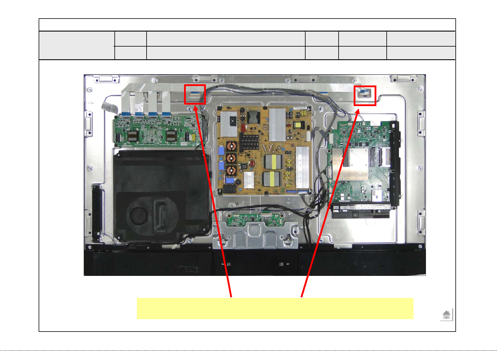
Standard Repair Process Detail Technical Manual
Copyright ⓒ 2012 LG Electronics. Inc. All right reserved.
Only for training and service purposes
LGE Internal Use Only
LCD TV
<XXLM9600>
Error
symptom
Content
A. Video error_No video/Normal audio
Check LCD back light with naked eye
Established
date
Revised
date
2011. 12 .14
A1
After turning on the power and disassembling the case, check with the naked eye,
whether you can see light from 2 locations.
A1
Page 89
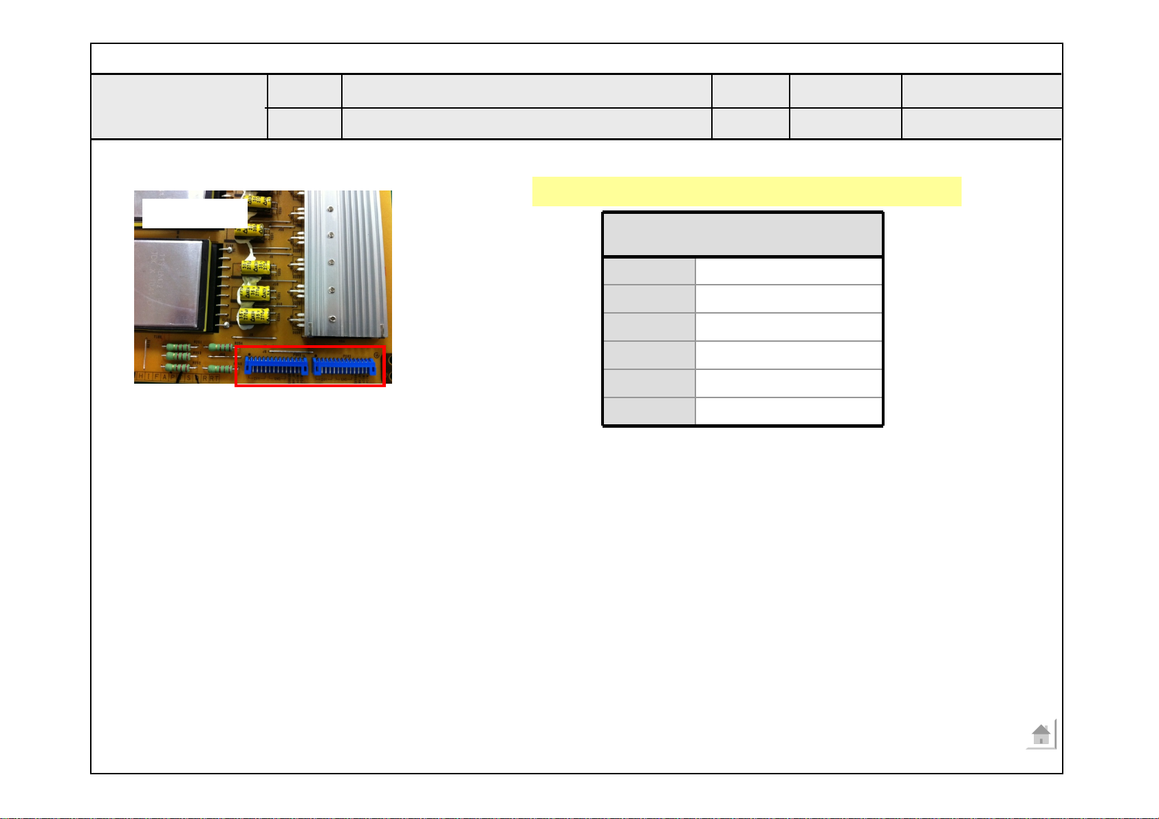
Standard Repair Process Detail Technical Manual
Copyright ⓒ 2012 LG Electronics. Inc. All right reserved.
Only for training and service purposes
LGE Internal Use Only
LCD TV
ALEF LED
Error
symptom
Content
A. Video error_No video/Normal audio
LED driver B+ 24V measuring method
Check the DC 24V and Inverter on
Established
date
Revised
date
14 Pin
(Power Board ↔ Driver) PSU
1 ~ 5 24V
6 ~ 10 GND
11 Detect
12 Inverter On/Off
13 Int. PWM
14 Ext. PWM (PDIM)
2011. 12 .14
A2
A2
Page 90
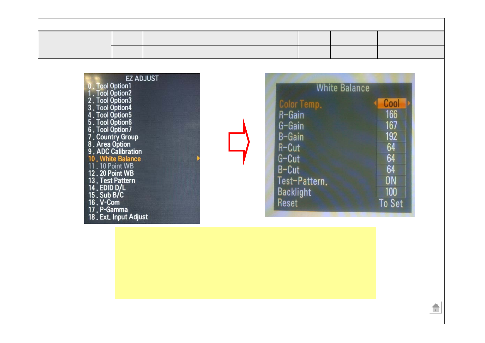
Standard Repair Process Detail Technical Manual
Copyright ⓒ 2012 LG Electronics. Inc. All right reserved.
Only for training and service purposes
LGE Internal Use Only
LCD TV
<ALL MODELS>
Error
symptom
Content
A. Video error_No video/Normal audio
Check White Balance value
Established
date
Revised
date
2011. 12 .14
A3
Entry method
Entry method
1. Press the ADJ button on the remote controller for adjustment.
1. Press the ADJ button on the remote controller for adjustment.
2. Enter into White Balance of item 6.
2. Enter into White Balance of item 10.
3. After recording the R, G, B (GAIN, Cut) value of Color Temp
3. After recording the R, G, B (GAIN, Cut) value of Color Temp
(Cool/Medium/Warm), re-enter the value after replacing the MAIN BOARD.
(Cool/Medium/Warm), re-enter the value after replacing the MAIN BOARD.
A3
Page 91
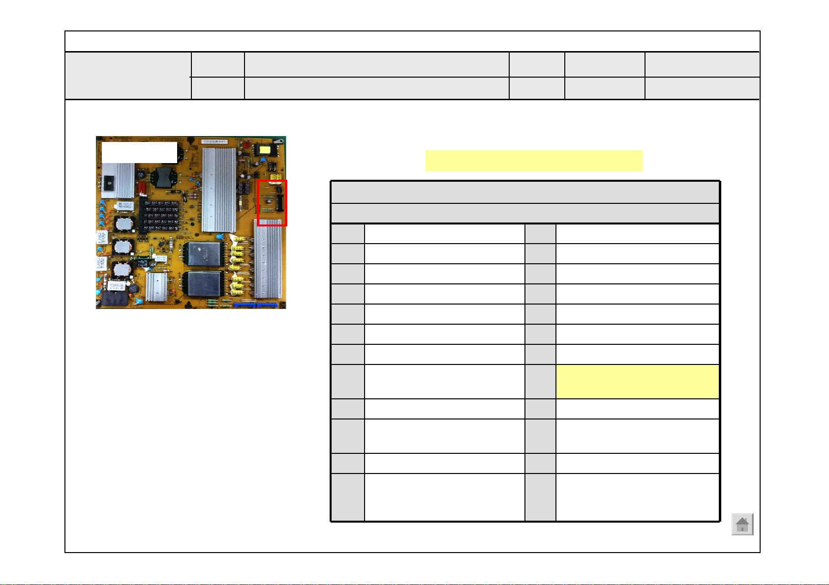
Standard Repair Process Detail Technical Manual
Copyright ⓒ 2012 LG Electronics. Inc. All right reserved.
Only for training and service purposes
LGE Internal Use Only
LCD TV
Error
symptom
Content
A. Video error_No video/ Audio
Power Board voltage measuring method
Established
date
Revised
date
2011. 12 .14
A4
ALEF LED
Check the DC 24V, 12V, 3.5V.
24 Pin (Power Board ↔ Main Board) - 공통
SMAW200-H24S (YEONHO)
1
3
5
7
9
11
13 GND 14
15 GND 16
17 12V 18
19 12V 20
Power on
20V (24V)
GND
GND
3.5V
3.5V
10
12
2
4
6
8
20V (24V)
20V (24V)
GND
GND
3.5V
3.5V
GND
N.C
(Only LPB : V-sync)
Inverter On/off
N.C
(LPB, Lamp : A-dim)
21 12V 22
23 N.C
(only Lamp SCANNING Model
: PWM Dim #2)
24 Error-out
A4
PWM Dim #1
Page 92
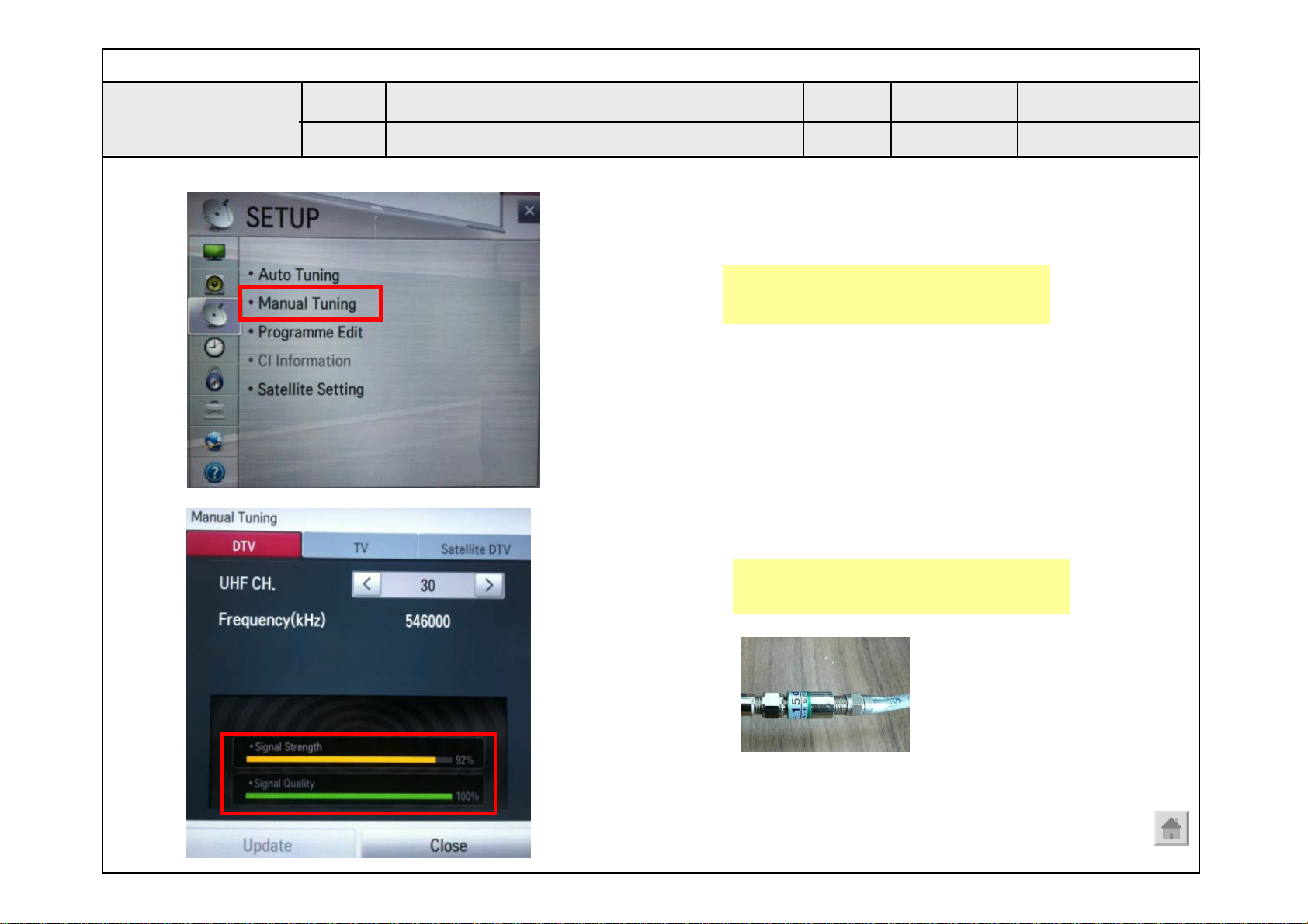
Standard Repair Process Detail Technical Manual
Copyright ⓒ 2012 LG Electronics. Inc. All right reserved.
Only for training and service purposes
LGE Internal Use Only
LCD TV
<ALL MODELS>
Error
symptom
Content
A. Video error_Video error, video lag/stop
TUNER input signal strength checking method
Established
date
Revised
date
2011. 12 .14
Settings Æ Set up Æ Manual Tuning
Æ select channel
A6
When the signal is strong, use the
attenuator (-10dB, -15dB, -20dB etc.)
A6
Page 93
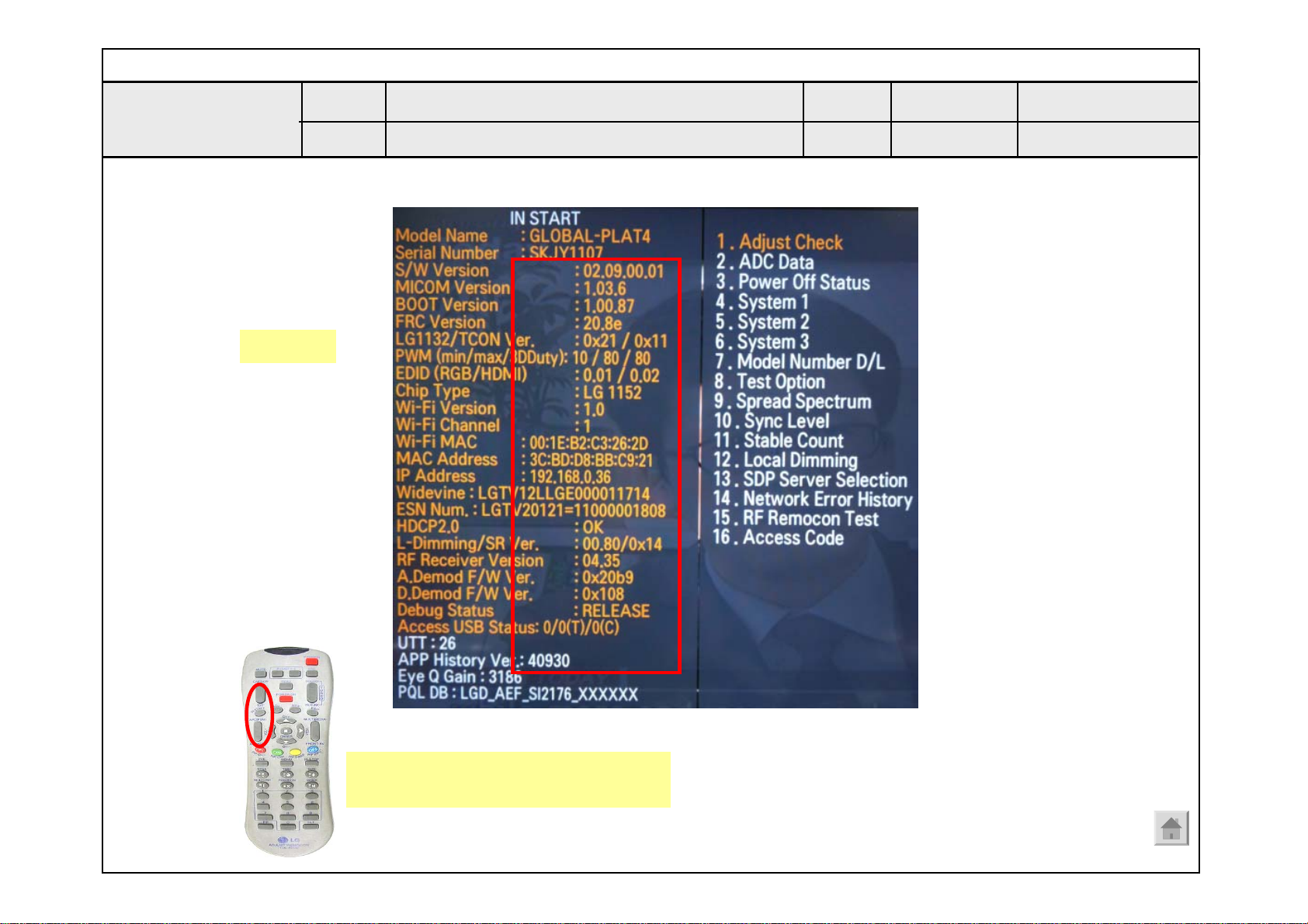
Standard Repair Process Detail Technical Manual
Copyright ⓒ 2012 LG Electronics. Inc. All right reserved.
Only for training and service purposes
LGE Internal Use Only
LCD TV
Error
symptom
Content
A. Video error_Video error, video lag/stop
LCD-TV Version checking method
Established
date
Revised
date
2011. 12 .14
A7
<ALL MODELS>
1. Checking method for remote controller for adjustment
Version
Press the IN-START with the
remote controller for adjustment
A7
Page 94
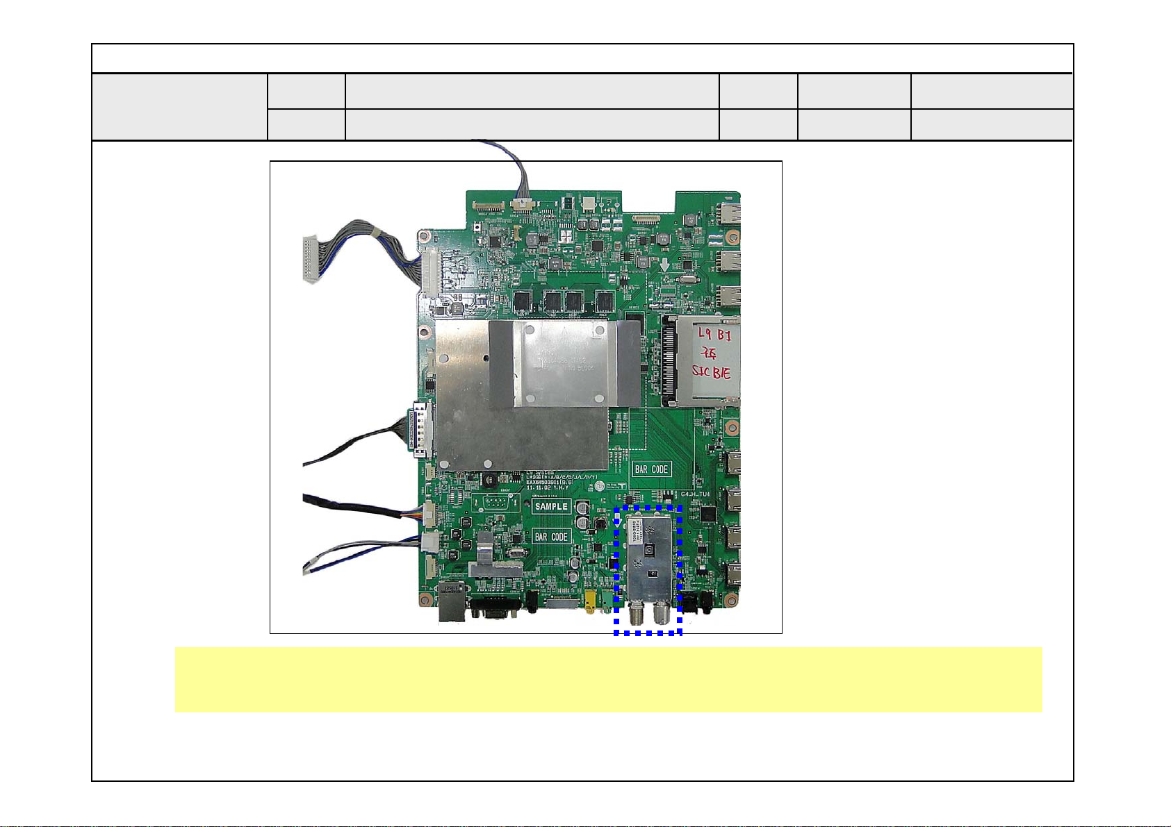
Standard Repair Process Detail Technical Manual
Copyright ⓒ 2012 LG Electronics. Inc. All right reserved.
Only for training and service purposes
LGE Internal Use Only
LCD TV
<ALL MODELS>
Error
symptom
Content
A. Video error_Video error, video lag/stop
TUNER checking part
Established
date
Revised
date
2011. 12 .14
A8
Checking method:
1. Check the signal strength or check whether the screen is normal when the external device is connected.
2. After measuring each voltage from power supply, finally replace the MAIN BOARD.
A8
Page 95
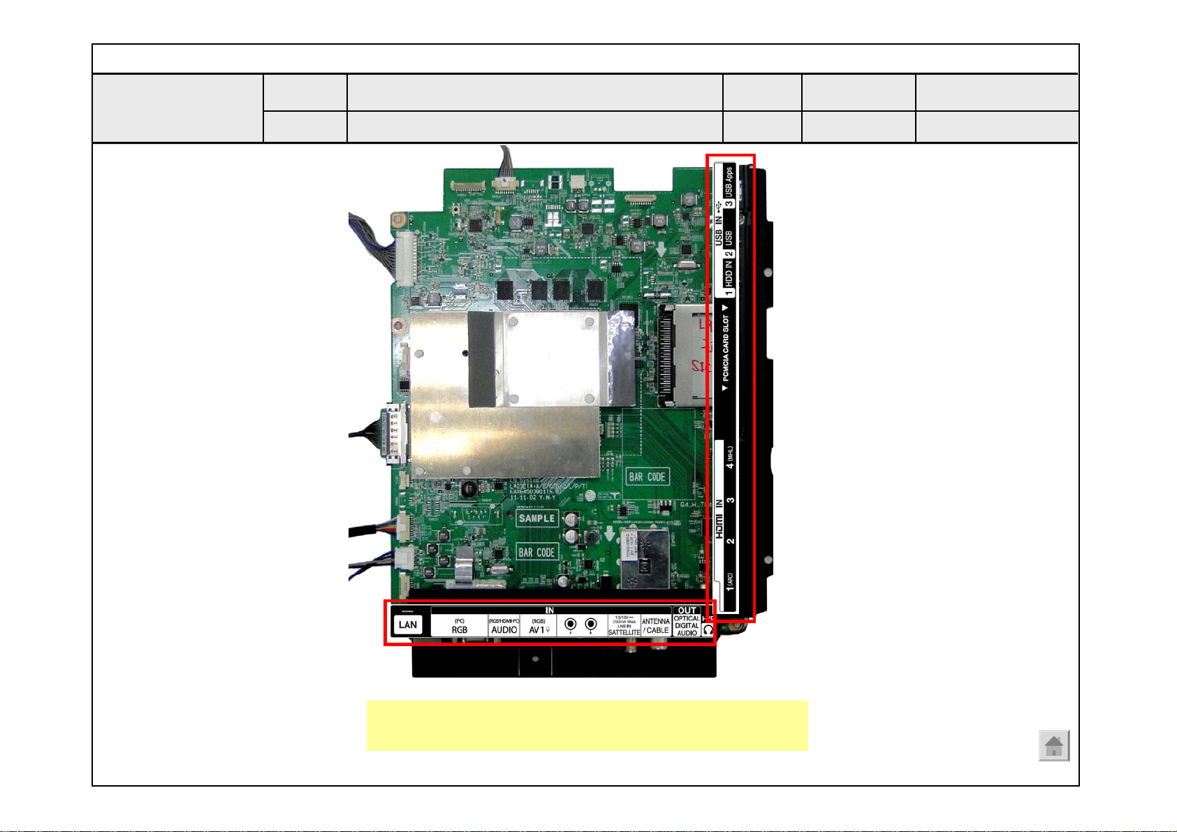
Standard Repair Process Detail Technical Manual
Copyright ⓒ 2012 LG Electronics. Inc. All right reserved.
Only for training and service purposes
LGE Internal Use Only
LCD TV
<ALL MODELS>
Error
symptom
Content
A. Video error _Vertical/Horizontal bar,
residual image, light spot
LCD TV connection diagram (1)
Established
date
Revised
date
2011. 12 .14
A9
As the part connecting to the external input, check
the screen condition by signal
A9
Page 96
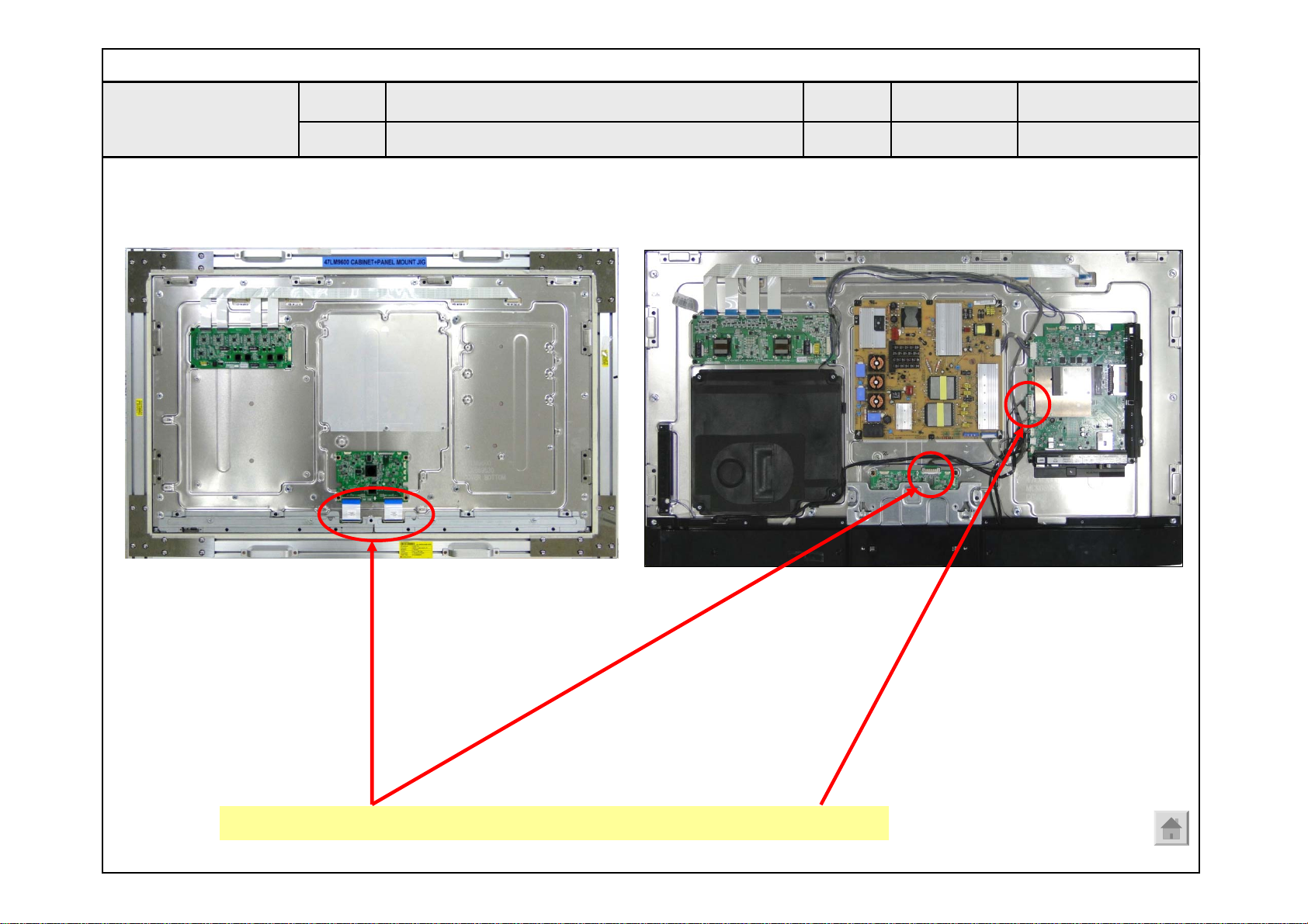
Standard Repair Process Detail Technical Manual
Copyright ⓒ 2012 LG Electronics. Inc. All right reserved.
Only for training and service purposes
LGE Internal Use Only
LCD TV
<ALL MODELS>
Error
symptom
Content
Check Link Cable (LVDS) reconnection condition
A. Video error_Color error
Established
date
Revised
date
2011. 12 .14
A10
Check the contact condition of the Link Cable, especially dust or mis insertion.
A10
Page 97
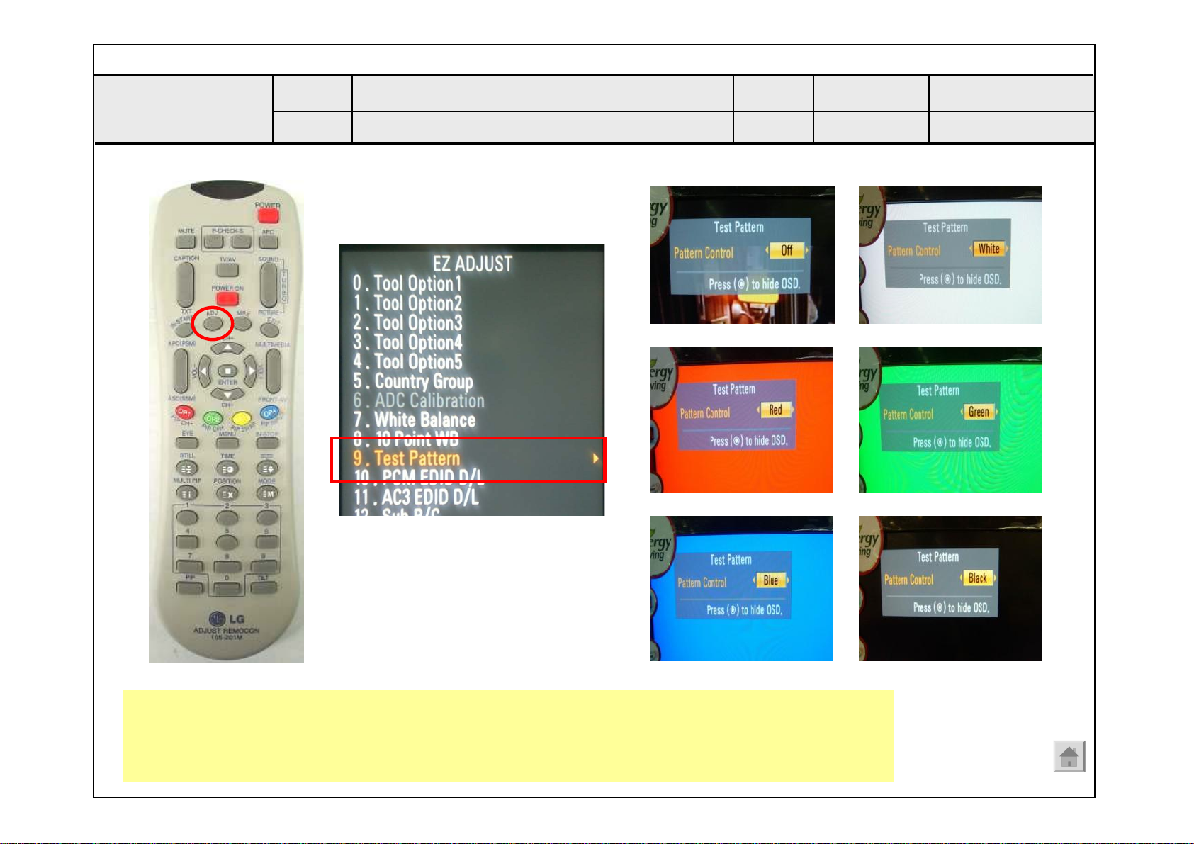
Standard Repair Process Detail Technical Manual
Copyright ⓒ 2012 LG Electronics. Inc. All right reserved.
Only for training and service purposes
LGE Internal Use Only
LCD TV
Error
symptom
Content
A. Video error_Color error
Adjustment Test pattern - ADJ Key
Established
date
Revised
date
2011. 12 .14
A12
You can view 6 types of patterns using the ADJ Key
Checking item : 1. Defective pixel 2. Residual image 3. MODULE error (ADD-BAR,SCAN BAR..)
4.Video error (Classification of MODULE or Main-B/D!)
A12
Page 98
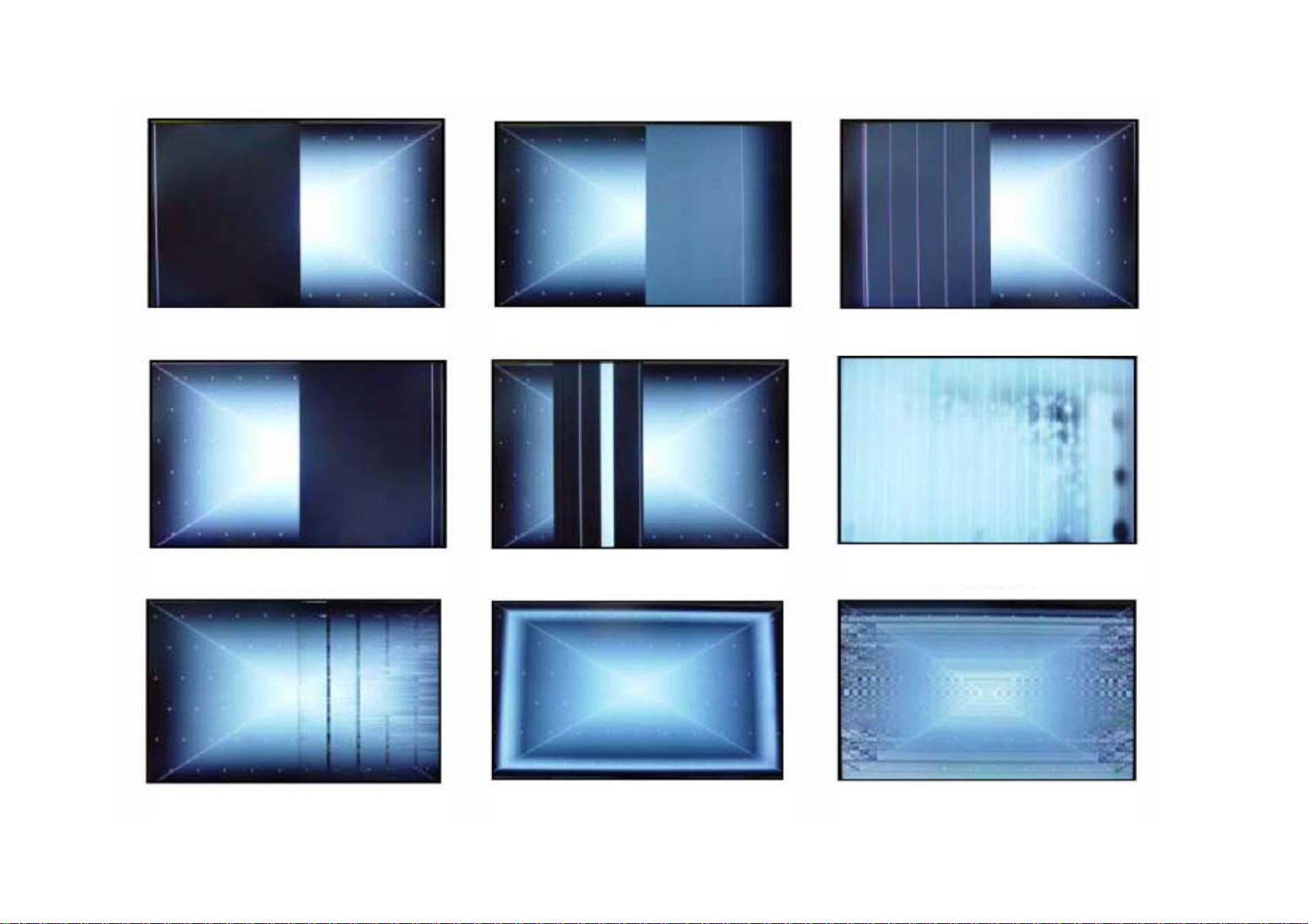
Appendix : Exchange T-Con Board (1)
Copyright ⓒ 2012 LG Electronics. Inc. All right reserved.
Only for training and service purposes
LGE Internal Use Only
Solder defect, CNT Broken
Solder defect, CNT Broken
Solder defect, CNT Broken
T-Con Defect, CNT Broken
T-Con Defect, CNT Broken
Solder defect, CNT Broken
T-Con Defect, CNT Broken
Solder defect, CNT Broken
Abnormal Power Section
Solder defect, Short/Crack
Abnormal Power Section Solder defect, Short/Crack
A - 1/5
Page 99
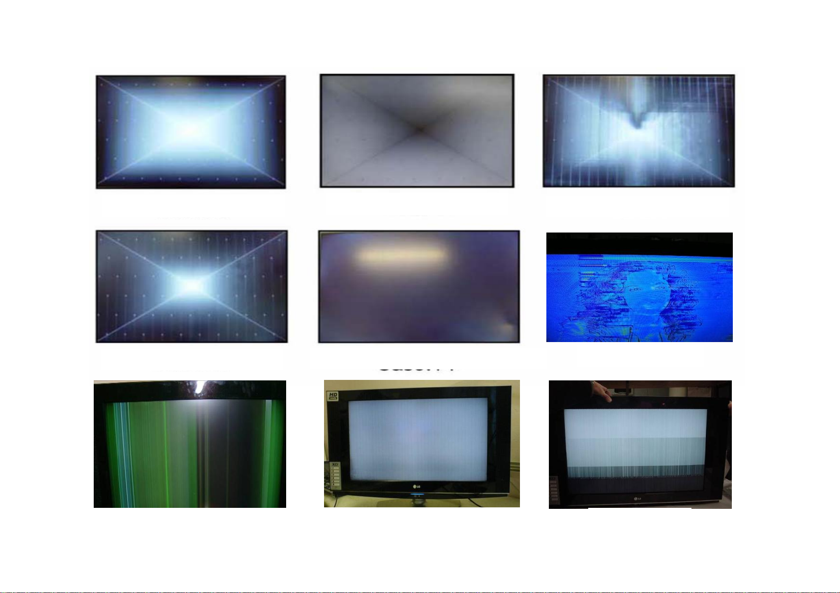
Appendix : Exchange T-Con Board (2)
Copyright ⓒ 2012 LG Electronics. Inc. All right reserved.
Only for training and service purposes
LGE Internal Use Only
Abnormal Power Section
Solder defect, Short/Crack
Abnormal Power Section
Fuse Open, Abnormal power section
Solder defect, Short/Crack
Abnormal Display
GRADATION
Noise
A - 2/5
GRADATION
Page 100
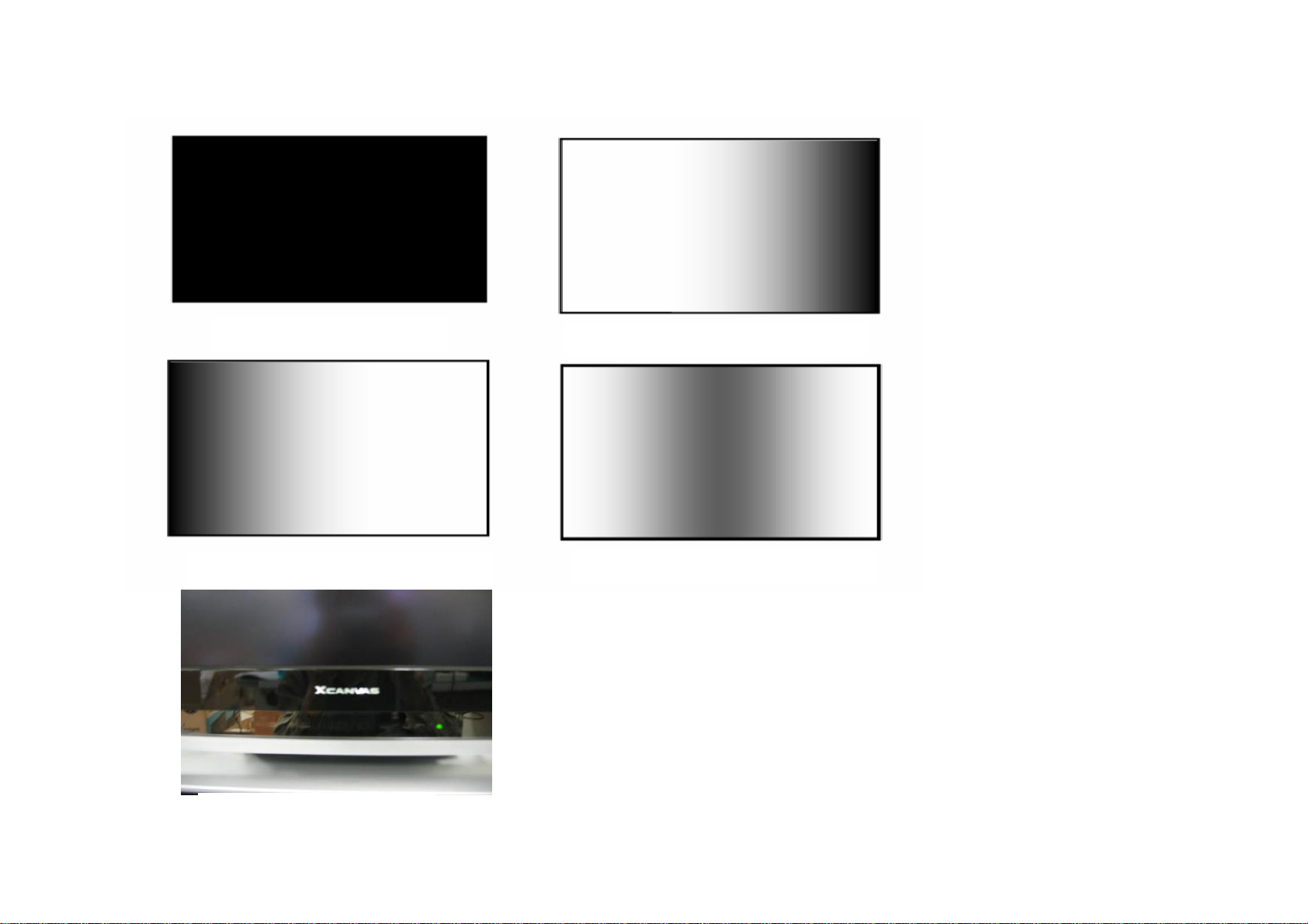
Appendix : Exchange LED driver Board (PSU)
Copyright ⓒ 2012 LG Electronics. Inc. All right reserved.
Only for training and service purposes
LGE Internal Use Only
No Light
Dim Light
Dim Light
Dim Light
No picture/Sound Ok
A - 3/5
 Loading...