

Page 1
TV COM1 COM2AV1 AV2 RGB
WIRELESS
1 2 3 4
4
LCD TV
SERVICE MANUAL
CAUTION
BEFORE SERVICING THE CHASSIS,
READ THE SAFETY PRECAUTIONS IN THIS MANUAL.
CHASSIS : LC91E
MODEL : 55LH95QD
North/Latin America http://aic.lgservice.com
Europe/Africa http://eic.lgservice.com
Asia/Oceania http://biz.lgservice.com
Internal Use Only
Printed in KoreaP/NO : MFL60021630 (0909-REV00)
55LH95QD-AA
Page 2

- 2 -
Copyright © 2009 LG Electronics. Inc. All right reserved.
Only for training and service purposes
LGE Internal Use Only
CONTENTS
CONTENTS ............................................................................................. 2
PRODUCT SAFETY ................................................................................. 3
SPECIFICATION ....................................................................................... 6
ADJUSTMENT INSTRUCTION ................................................................ 9
MEDIA-BOX SETUP GUIDE .................................................................. 14
EXPLODED VIEW .................................................................................. 15
SVC. SHEET ...............................................................................................
Page 3
- 3 -
Copyright © 2009 LG Electronics. Inc. All right reserved.
Only for training and service purposes
LGE Internal Use Only
SAFETY PRECAUTIONS
Many electrical and mechanical parts in this chassis have special safety-related characteristics. These parts are identified by in the
Schematic Diagram and Exploded View.
It is essential that these special safety parts should be replaced with the same components as recommended in this manual to prevent
Shock, Fire, or other Hazards.
Do not modify the original design without permission of manufacturer.
General Guidance
An isolation Transformer should always be used during the
servicing of a receiver whose chassis is not isolated from the AC
power line. Use a transformer of adequate power rating as this
protects the technician from accidents resulting in personal injury
from electrical shocks.
It will also protect the receiver and it's components from being
damaged by accidental shorts of the circuitry that may be
inadvertently introduced during the service operation.
If any fuse (or Fusible Resistor) in this TV receiver is blown,
replace it with the specified.
When replacing a high wattage resistor (Oxide Metal Film Resistor,
over 1W), keep the resistor 10mm away from PCB.
Keep wires away from high voltage or high temperature parts.
Before returning the receiver to the customer,
always perform an AC leakage current check on the exposed
metallic parts of the cabinet, such as antennas, terminals, etc., to
be sure the set is safe to operate without damage of electrical
shock.
Leakage Current Cold Check(Antenna Cold Check)
With the instrument AC plug removed from AC source, connect an
electrical jumper across the two AC plug prongs. Place the AC
switch in the on position, connect one lead of ohm-meter to the AC
plug prongs tied together and touch other ohm-meter lead in turn to
each exposed metallic parts such as antenna terminals, phone
jacks, etc.
If the exposed metallic part has a return path to the chassis, the
measured resistance should be between 1MΩ and 5.2MΩ.
When the exposed metal has no return path to the chassis the
reading must be infinite.
An other abnormality exists that must be corrected before the
receiver is returned to the customer.
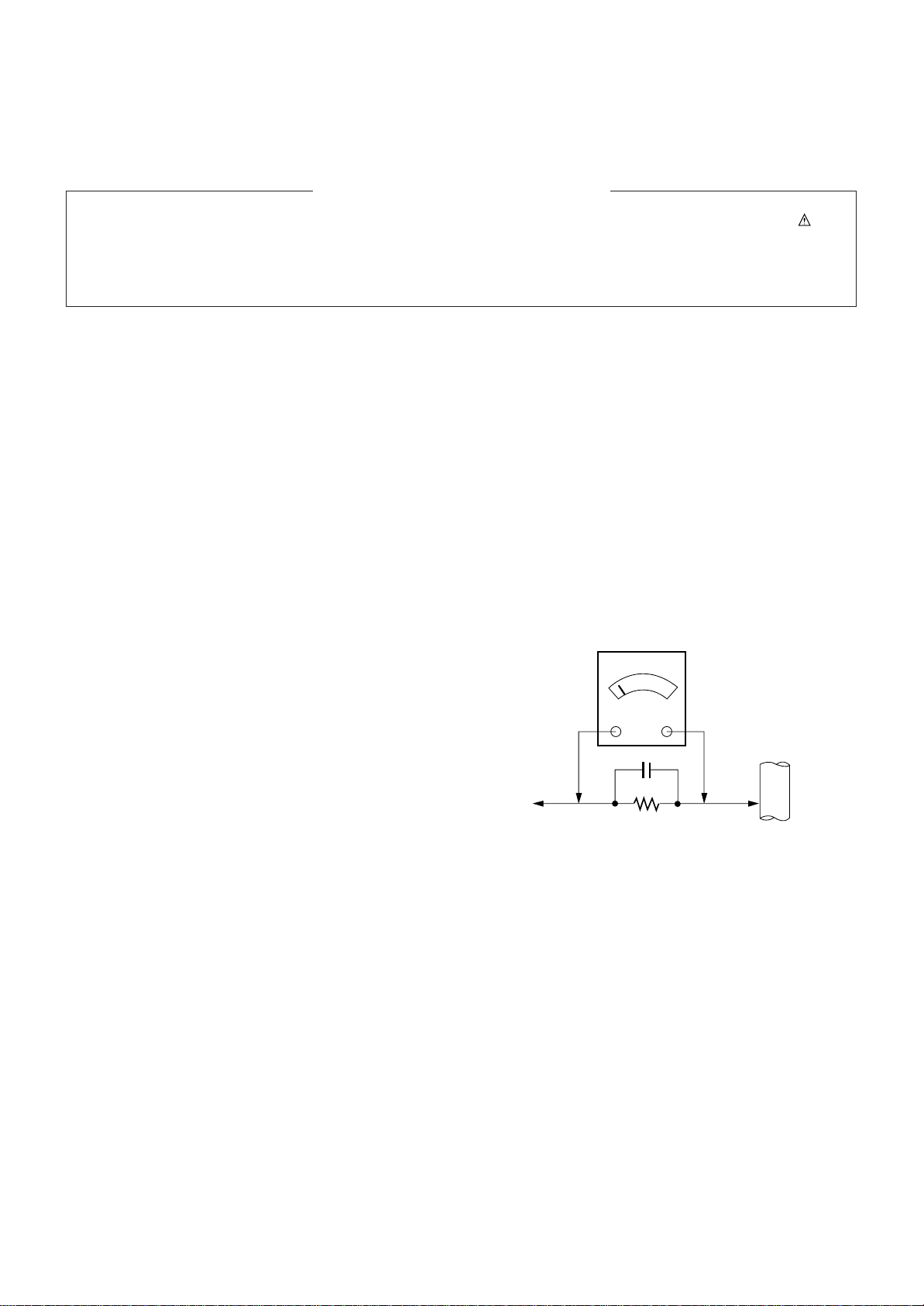
Leakage Current Hot Check (See below Figure)
Plug the AC cord directly into the AC outlet.
Do not use a line Isolation Transformer during this check.
Connect 1.5K/10watt resistor in parallel with a 0.15uF capacitor
between a known good earth ground (Water Pipe, Conduit, etc.)
and the exposed metallic parts.
Measure the AC voltage across the resistor using AC voltmeter
with 1000 ohms/volt or more sensitivity.
Reverse plug the AC cord into the AC outlet and repeat AC voltage
measurements for each exposed metallic part. Any voltage
measured must not exceed 0.75 volt RMS which is corresponds to
0.5mA.
In case any measurement is out of the limits specified, there is
possibility of shock hazard and the set must be checked and
repaired before it is returned to the customer.
Leakage Current Hot Check circuit
1.5 Kohm/10W
To Instrument's
exposed
METALLIC PARTS
Good Earth Ground
such as WATER PIPE,
CONDUIT etc.
AC Volt-meter
IMPORTANT SAFETY NOTICE
0.15uF
Page 4

Copyright © 2009 LG Electronics. Inc. All right reserved.
Only for training and service purposes
LGE Internal Use Only
- 4 -
CAUTION: Before servicing receivers covered by this service
manual and its supplements and addenda, read and follow the
SAFETY PRECAUTIONS on page 3 of this publication.
NOTE: If unforeseen circumstances create conflict between the
following servicing precautions and any of the safety precautions on
page 3 of this publication, always follow the safety precautions.
Remember: Safety First.
General Servicing Precautions
1. Always unplug the receiver AC power cord from the AC power
source before;
a. Removing or reinstalling any component, circuit board
module or any other receiver assembly.
b. Disconnecting or reconnecting any receiver electrical plug or
other electrical connection.
c. Connecting a test substitute in parallel with an electrolytic
capacitor in the receiver.
CAUTION: A wrong part substitution or incorrect polarity
installation of electrolytic capacitors may result in an
explosion hazard.
2. Test high voltage only by measuring it with an appropriate high
voltage meter or other voltage measuring device (DVM,
FETVOM, etc) equipped with a suitable high voltage probe.
Do not test high voltage by "drawing an arc".
3. Do not spray chemicals on or near this receiver or any of its
assemblies.
4. Unless specified otherwise in this service manual, clean
electrical contacts only by applying the following mixture to the
contacts with a pipe cleaner, cotton-tipped stick or comparable
non-abrasive applicator; 10% (by volume) Acetone and 90% (by
volume) isopropyl alcohol (90%-99% strength)
CAUTION: This is a flammable mixture.
Unless specified otherwise in this service manual, lubrication of
contacts in not required.
5. Do not defeat any plug/socket B+ voltage interlocks with which
receivers covered by this service manual might be equipped.
6. Do not apply AC power to this instrument and/or any of its
electrical assemblies unless all solid-state device heat sinks are
correctly installed.
7. Always connect the test receiver ground lead to the receiver
chassis ground before connecting the test receiver positive
lead.
Always remove the test receiver ground lead last.
8. Use with this receiver only the test fixtures specified in this
service manual.
CAUTION: Do not connect the test fixture ground strap to any
heat sink in this receiver.
Electrostatically Sensitive (ES) Devices
Some semiconductor (solid-state) devices can be damaged easily
by static electricity. Such components commonly are called
Electrostatically Sensitive (ES) Devices. Examples of typical ES
devices are integrated circuits and some field-effect transistors and
semiconductor "chip" components. The following techniques
should be used to help reduce the incidence of component
damage caused by static by static electricity.
1. Immediately before handling any semiconductor component or
semiconductor-equipped assembly, drain off any electrostatic
charge on your body by touching a known earth ground.
Alternatively, obtain and wear a commercially available
discharging wrist strap device, which should be removed to
prevent potential shock reasons prior to applying power to the
unit under test.
2. After removing an electrical assembly equipped with ES
devices, place the assembly on a conductive surface such as
aluminum foil, to prevent electrostatic charge buildup or
exposure of the assembly.
3. Use only a grounded-tip soldering iron to solder or unsolder ES
devices.
4. Use only an anti-static type solder removal device. Some solder
removal devices not classified as "anti-static" can generate
electrical charges sufficient to damage ES devices.
5. Do not use freon-propelled chemicals. These can generate
electrical charges sufficient to damage ES devices.
6. Do not remove a replacement ES device from its protective
package until immediately before you are ready to install it.
(Most replacement ES devices are packaged with leads
electrically shorted together by conductive foam, aluminum foil
or comparable conductive material).
7. Immediately before removing the protective material from the
leads of a replacement ES device, touch the protective material
to the chassis or circuit assembly into which the device will be
installed.
CAUTION: Be sure no power is applied to the chassis or circuit,
and observe all other safety precautions.
8. Minimize bodily motions when handling unpackaged
replacement ES devices. (Otherwise harmless motion such as
the brushing together of your clothes fabric or the lifting of your
foot from a carpeted floor can generate static electricity
sufficient to damage an ES device.)
General Soldering Guidelines
1. Use a grounded-tip, low-wattage soldering iron and appropriate
tip size and shape that will maintain tip temperature within the
range or 500
°F to 600°F.
2. Use an appropriate gauge of RMA resin-core solder composed
of 60 parts tin/40 parts lead.
3. Keep the soldering iron tip clean and well tinned.
4. Thoroughly clean the surfaces to be soldered. Use a mall wirebristle (0.5 inch, or 1.25cm) brush with a metal handle.
Do not use freon-propelled spray-on cleaners.
5. Use the following unsoldering technique
a. Allow the soldering iron tip to reach normal temperature.
(500
°F to 600°F)
b. Heat the component lead until the solder melts.
c. Quickly draw the melted solder with an anti-static, suction-
type solder removal device or with solder braid.
CAUTION: Work quickly to avoid overheating the circuit
board printed foil.
6. Use the following soldering technique.
a. Allow the soldering iron tip to reach a normal temperature
(500
°F to 600°F)
b. First, hold the soldering iron tip and solder the strand against
the component lead until the solder melts.
c. Quickly move the soldering iron tip to the junction of the
component lead and the printed circuit foil, and hold it there
only until the solder flows onto and around both the
component lead and the foil.
CAUTION: Work quickly to avoid overheating the circuit
board printed foil.
d. Closely inspect the solder area and remove any excess or
splashed solder with a small wire-bristle brush.
SERVICING PRECAUTIONS
Page 5

- 5 -
Copyright © 2009 LG Electronics. Inc. All right reserved.
Only for training and service purposes
LGE Internal Use Only
IC Remove/Replacement
Some chassis circuit boards have slotted holes (oblong) through
which the IC leads are inserted and then bent flat against the
circuit foil. When holes are the slotted type, the following technique
should be used to remove and replace the IC. When working with
boards using the familiar round hole, use the standard technique
as outlined in paragraphs 5 and 6 above.
Removal
1. Desolder and straighten each IC lead in one operation by gently
prying up on the lead with the soldering iron tip as the solder
melts.
2. Draw away the melted solder with an anti-static suction-type
solder removal device (or with solder braid) before removing the
IC.
Replacement
1. Carefully insert the replacement IC in the circuit board.
2. Carefully bend each IC lead against the circuit foil pad and
solder it.
3. Clean the soldered areas with a small wire-bristle brush.
(It is not necessary to reapply acrylic coating to the areas).
"Small-Signal" Discrete Transistor
Removal/Replacement
1. Remove the defective transistor by clipping its leads as close as
possible to the component body.
2. Bend into a "U" shape the end of each of three leads remaining
on the circuit board.
3. Bend into a "U" shape the replacement transistor leads.
4. Connect the replacement transistor leads to the corresponding
leads extending from the circuit board and crimp the "U" with
long nose pliers to insure metal to metal contact then solder
each connection.
Power Output, Transistor Device
Removal/Replacement
1. Heat and remove all solder from around the transistor leads.
2. Remove the heat sink mounting screw (if so equipped).
3. Carefully remove the transistor from the heat sink of the circuit
board.
4. Insert new transistor in the circuit board.
5. Solder each transistor lead, and clip off excess lead.
6. Replace heat sink.
Diode Removal/Replacement
1. Remove defective diode by clipping its leads as close as
possible to diode body.
2. Bend the two remaining leads perpendicular y to the circuit
board.
3. Observing diode polarity, wrap each lead of the new diode
around the corresponding lead on the circuit board.
4. Securely crimp each connection and solder it.
5. Inspect (on the circuit board copper side) the solder joints of
the two "original" leads. If they are not shiny, reheat them and if
necessary, apply additional solder.
Fuse and Conventional Resistor
Removal/Replacement
1. Clip each fuse or resistor lead at top of the circuit board hollow
stake.
2. Securely crimp the leads of replacement component around
notch at stake top.
3. Solder the connections.
CAUTION: Maintain original spacing between the replaced
component and adjacent components and the circuit board to
prevent excessive component temperatures.
Circuit Board Foil Repair
Excessive heat applied to the copper foil of any printed circuit
board will weaken the adhesive that bonds the foil to the circuit
board causing the foil to separate from or "lift-off" the board. The
following guidelines and procedures should be followed whenever
this condition is encountered.
At IC Connections
To repair a defective copper pattern at IC connections use the
following procedure to install a jumper wire on the copper pattern
side of the circuit board. (Use this technique only on IC
connections).
1. Carefully remove the damaged copper pattern with a sharp
knife. (Remove only as much copper as absolutely necessary).
2. carefully scratch away the solder resist and acrylic coating (if
used) from the end of the remaining copper pattern.
3. Bend a small "U" in one end of a small gauge jumper wire and
carefully crimp it around the IC pin. Solder the IC connection.
4. Route the jumper wire along the path of the out-away copper
pattern and let it overlap the previously scraped end of the good
copper pattern. Solder the overlapped area and clip off any
excess jumper wire.
At Other Connections
Use the following technique to repair the defective copper pattern
at connections other than IC Pins. This technique involves the
installation of a jumper wire on the component side of the circuit
board.
1. Remove the defective copper pattern with a sharp knife.
Remove at least 1/4 inch of copper, to ensure that a hazardous
condition will not exist if the jumper wire opens.
2. Trace along the copper pattern from both sides of the pattern
break and locate the nearest component that is directly
connected to the affected copper pattern.
3. Connect insulated 20-gauge jumper wire from the lead of the
nearest component on one side of the pattern break to the lead
of the nearest component on the other side.
Carefully crimp and solder the connections.
CAUTION: Be sure the insulated jumper wire is dressed so the
it does not touch components or sharp edges.
Page 6

Copyright © 2009 LG Electronics. Inc. All right reserved.
Only for training and service purposes
LGE Internal Use Only
- 6 -
4. General Specification(TV)
No. Item Specification Remark
1. Receiving System Analog : Upper Heterodyne
Digital : COFDM, QAM
2. Input Voltage 100- 240V~, 50/60Hz
3. Market China
4. Screen Size 55 inch Wide (1920 x 1080) FHD
5. Aspect Ratio 16:9
6. Broadcasting systme 1) PAL-DK
2) PAL-I
3) NTSC-M
4) DTMB
5) DVB-C
7. LCD Module LC550WUL-SBT1 LGD
8. Operating Environment 1) Temp : 0 ~ 40 deg
2) Humidity : ~ 80 %
9. Storage Environment 1) Temp : -20 ~ 60 deg
2) Humidity : 0 ~ 85 %
1. Application Range
This specification sheet is applied to the LCD TV used LC91E
chassis.
2. Specification
Each part is tested as below without special appointment
1) Temperature : 25 ± 5°C (77 ± 9ºF), CST : 40 ± 5ºC
2) Relative Humidity : 65 ±10%
3) Power Voltage : Standard input voltage
(100-240V@ 50/60Hz)
* Standard Voltage of each products is marked by models
4) Specification and performance of each parts are followed
each drawing and specification by part number in
accordance with BOM.
5) The receiver must be operated for about 20 minutes prior to
the adjustment.
3. Test method
1) Performance : LGE TV test method followed.
2) Demanded other specification
- Safety : CE, IEC specification
- EMC : CE, IEC specification
SPECIFICATION
NOTE : Specifications and others are subject to change without notice for improvement
.
Page 7

Copyright © 2009 LG Electronics. Inc. All right reserved.
Only for training and service purposes
LGE Internal Use Only
- 7 -
5. Chroma & Brightness
No Item Min. Typ. Max. Unit Remark
1 Max Luminance 400 500 cd/m
2
(Center 1-point / Full White Pattern)
2 Luminance uniformity 77 % Full white
3 Response Time Gray-to-Gray 5 8 ms Picture mode : Cinema
MPRT 8 10 ms
4 Color coordinate RED X 0.645 Typ.
Y 0.330 ± 0.03
GREEN X 0.297
Y 0.629 Color Coordinate Measurement
BLUE X 0.146 Mode : PC
Y 0.054 PSM : Standard
WHITE X 0.279 CSM : Medium
Y 0.292
5 Contrast ratio 900:1 1300:1 Local Dimming ON
(Except RGB/HDMI-PC)
4,500,000 5,000,000 DCR(Except RGB/HDMI-PC)
6 Color Temperature Cool X 0.254 0.269 0.284 <Test Condition>
Y 0.258 0.273 0.288 85% Full white pattern
Medium X 0.270 0.285 0.300
Y 0.278 0.293 0.308
Warm X 0.298 0.313 0.328
Y 0.314 0.329 0.344
7 Color Distortion, DG 10 %
8 Color Distortion, DP 10 deg
9 Color S/N, AM/FM 43.0 dB
10 Color Killer Sensitivity -80 dBm
6. Component Video Input (Y, CB/PB, CR/PR)
No.
Specification
Remark
Resolution H-freq(kHz) V-freq(Hz) Pixel clock
1. 720x480 15.73 60.00 SDTV, DVD 480i
2 720x480 15.63 59.94 SDTV, DVD 480i
3 720x480 31.47 59.94 480p
4 720x480 31.50 60.00 480p
5 720x576 15.625 50.00 SDTV, DVD 625 Line
6 720x576 31.25 50.00 HDTV 576p
7 1280x720 45.00 50.00 HDTV 720p
8 1280x720 44.96 59.94 HDTV 720p
9 1280x720 45.00 60.00 HDTV 720p
10. 1920x1080 31.25 50.00 HDTV 1080i
11. 1920x1080 33.75 60.00 HDTV 1080i
12. 1920x1080 33.72 59.94 HDTV 1080i
13. 1920x1080 56.250 50 HDTV 1080p
14. 1920x1080 67.43/67.5 59.94/60 HDTV 1080p
Page 8
Copyright © 2009 LG Electronics. Inc. All right reserved.
Only for training and service purposes
LGE Internal Use Only
- 8 -
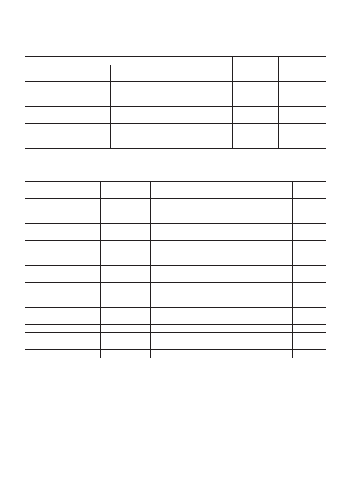
No. Specification
Proposed Remark
Resolution H-freq(kHz) V-freq(Hz) Pixel clock(MHz)
PC
1. 720*400 31.468 70.08 28.321 HDCP
2. 640*480 31.469 59.94 25.17 VESA HDCP
3 800*600 37.879 60.31 40.00 VESA HDCP
4. 1024*768 48.363 60.00 65.00 VESA(XGA) HDCP
5. 1280*768 47.78 59.87 79.5 WXGA HDCP
6. 1360*768 47.72 59.8 84.75 WXGA HDCP
7. 1280*1024 63981 60.0 108.875 SXGA HDCP
8. 1920*1080 67.5 60 148.5 WUXGA HDCP
7. RGB input (PC)
8. HDMI input (PC/DTV)
No. Resolution H-freq(kHz) V-freq(Hz) Pixel clock(MHz) Proposed Remark
DTV
1. 720*480 31.469 / 31.5 59.94 / 60 27.00/27.03 SDTV 480P
2. 720*576 31.25 50 54 SDTV 576P
3. 1280*720 37.500 50 74.25 HDTV 720P
4. 1280*720 44.96 / 45 59.94 / 60 74.17/74.25 HDTV 720P
5. 1920*1080 33.72 / 33.75 59.94 / 60 74.17/74.25 HDTV 1080I
6. 1920*1080 28.125 50.00 74.25 HDTV 1080I
7. 1920*1080 26.97 / 27 23.97 / 24 74.17/74.25 HDTV 1080P
8. 1920*1080 33.716 / 33.75 29.976 / 30.00 74.25 HDTV 1080P
9 1920*1080 56.250 50 148.5 HDTV 1080P
10. 1920*1080 67.43 / 67.5 59.94 / 60 148.35/148.50 HDTV 1080P
PC
1. 720*400 31.468 70.08 28.321 HDCP
2. 640*480 31.469 59.94 25.17 VESA HDCP
3 800*600 37.879 60.31 40.00 VESA HDCP
4. 1024*768 48.363 60.00 65.00 VESA(XGA) HDCP
5. 1280*768 47.78 59.87 79.5 WXGA HDCP
6. 1360*768 47.72 59.8 84.75 WXGA HDCP
7. 1280*1024 63.981 60.0 108.875 SXGA HDCP
8. 1920*1080 67.5 60 148.5 WUXGA HDCP
Page 9

1. Application Object
This specification sheet applied to LC91E Chassis applied
LCD TV all models manufactured in TV factory.
2. Notes
(1) Because this is not a hot chassis, it is not necessary to use
an isolation transformer. However, the use of isolation
transformer will help protect test equipment.
(2) Adjustments must be done in the correct order.
(3) The adjustments must be performed in the circumstance of
25±5°C of temperature and 65±10% of relative humidity if
there is no specific designation.
(4) The input voltage of the receiver be must kept 100V-240V,
50/60Hz when adjusting.
(5) The receiver must be operated for about 5 minutes prior to
the adjustment when module is in the circumstance of over
15ºC.
In case of keeping module is in the circumstance of 0°C, it
should be placed in the circumstance of above 15°C for 2
hours
In case of keeping module is in the circumstance of below
-20°C, it should be placed in the circumstance of above
15°C for 3 hours,.
(6) The TV and the Media-box must be connected by Wireless
or Wire. : Even if there is only the TV set, it is possible to
adjust the White-balance
- Entry process of White Pattern
1) Press the POWER ON key on R/C for adjustment.
2) Press the ADJ key on R/C and enter EZ ADJUST.
3) Select ‘7. Test Pattern’ by using CH +/- key and select
“White” by using VOL +/-.
* Set is activated HEAT RUN without signal generator in this
mode.
* Single color pattern (RED/BLUE/GREEN) of HEAT RUN
mode uses to check panel.
Caution : If the still image is displayed more than 20
minutes(Especially digital, cross hatch pattern), an afterimage in the black level area.
3. Adjustment items
- Check the TOOL OPTION prior to adjustment. If the TOOL
OPTION is incorrect, correct it then execute the power off/on
to apply the modification (refer to 7.3 TOOL OPTION)
- In case of this chassis,
Set the Media-box option in connection with Wireless or
Wire.
Set the TV option in HDMI5 mode.(remove the wired HDMI
cable)
3.1 Board-level adjustment
- ADC adjustment (Media-Box ONLY)
- EDID/DDC download
* Manual ADC Confirmation : [IN-START] -> [1.Adjust Check]
- After Board level adjustment, set volume setting value 0
3.2 Final assembly adjustment
- White Balance adjustment
- RS-232C functionality check
- EYE-Q TEST
- Wireless Pairing (it is worked in the Wired status)
- Shipment mode setting (In-Stop)
4. Board-level adjustment
4.1. ADC(LGE3369) adjustment
(1) Overview
ADC adjustment is needed to find the optimum black level
and gain in Analog-to-Digital device and to compensate
RGB deviation.
(2) Equipment & Condition
1) Jig (RS-232C protocol)
2) External/Internal PATTERN
- Adjustment : ADC Comp Comp 480i
-> Using a Pattern Generator(MSPG-925FA - Model:
209 ,Pattern:65 or etc), enter component signals
like below image into the Media-box.
- Adjustment : ADC Comp 1080p / RGB
-> use the Internal Pattern
* External input Image
Copyright © 2009 LG Electronics. Inc. All right reserved.
Only for training and service purposes
LGE Internal Use Only
- 9 -
ADJUSTMENT INSTRUCTION
Page 10
(3) Adjustment
1) Method
- Using RS-232, adjust items listed in 3.1 in the other
shown in “4.1.3.3”
2) Adj. protocol
Ref.) ADC Adj. RS232C Protocol_Ver1.0
3) Adj. order
- aa 00 00 [Enter ADC adj. mode]
- xb 00 40 [Change input source to Component1(480i)]
- ad 00 10 [Adjust 480i Comp1]
- xb 00 60 [Change input source to RGB(1024*768)]
- ad 00 10 [Adjust 1024*768 RGB]
- ad 00 90 End adj.
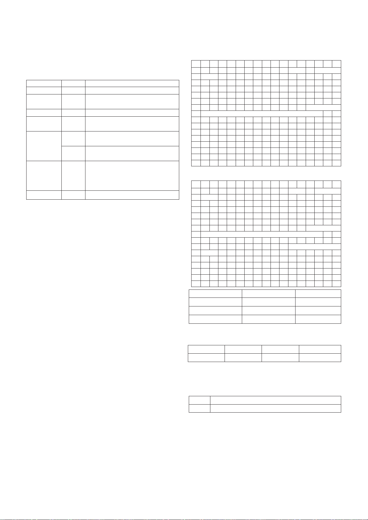
4.2. EDID(The Extended Display Identification
Data)/DDC(Display Data Channel) download
(1) Overview
It is a VESA regulation. A PC or a MNT will display an
optimal resolution through information sharing without any
necessity of user input. It is a realization of “Plug and Play”.
(2) Equipment
- Adjust remote control
- Since embedded EDID data is used, EDID download JIG,
HDMI cable and D-sub cable are not need.
(3)Download method
1) Press Adj. key on the Adj. R/C, then select “8.EDID
D/L”, By pressing Enter key, enter EDID D/L menu.
2) Select [Start] button by pressing Enter key, HDMI1 /
HDMI2 / HDMI3 / HDMI4 / RGB are Writing and display
OK or NG.
* For HDMI5 EDID D/L, Change the TV input mode into
HDMI5 mode then using Adj. R/C, download the HDMI5
EDID.
* HDMI5 / RGB can be downloaded by JIG and cable.
(4) EDID DATA
1) RGB EDID data
2) HDMI EDID data
* Detail EDID Options are below
ⓐ Product ID
ⓑ Serial No: Controlled on production line.
ⓒ Week, Year: Fixed as S/W released day
Week 0x02(2), Year : 0x13(2009)
ⓓ Model Name(Hex):
ⓔ Checksum: Changeable by total EDID data.
RGB 1D
HDMI1 04 F9
HDMI2 04 E9
HDMI3 04 D9
HDMI4 04 C9
- 10 -
Copyright © 2009 LG Electronics. Inc. All right reserved.
Only for training and service purposes
LGE Internal Use Only
Protocol Command Set ACK
Enter adj. mode aa 00 00 a 00 OK00x
Source change xb 00 40 b 00 OK40x (Adjust 480i Comp1 )
xb 00 60 b 00 OK60x (Adjust 1024*768 RGB)
Begin adj. ad 00 10
Return adj. result OKx (Case of Success)
NGx (Case of Fail)
Read adj. data (main) (main)
ad 00 20 000000000000000000000000007c007b006dx
(sub) (Sub)
ad 00 21 000000070000000000000000007c00830077x
Confirm adj. ad 00 99 NG 03 00x (Fail)
NG 03 01x (Fail)
NG 03 02x (Fail)
OK 03 03x (Success)
End adj. aa 00 90 a 00 OK90x
0123456789ABCDEF
00 00 FF FF FF FF FF FF 00 1E 6D ⓐⓑ
10 ⓒ 01 03 68 73 41 78 0A CF 74 A3 57 4C B0 23
20 09 48 4C A1 08 00 81 80 61 40 45 40 31 40 01 01
30 01 01 01 01 01 01 02 3A 80 18 71 38 2D 40 58 2C
40 45 00 7E 8A 42 00 00 1E 01 1D 00 72 51 D0 1E 20
50 6E 28 55 00 7E 8A 42 00 00 1E 00 00 00 FD 00 3A
60 3E 1E 53 10 00 0A 20 20 20 20 20 20 ⓓ
70 ⓓ 00 ⓔ
80 FF FF FF FF FF FF FF FF FF FF FF FF FF FF FF FF
90 FF FF FF FF FF FF FF FF FF FF FF FF FF FF FF FF
A0 FF FF FF FF FF FF FF FF FF FF FF FF FF FF FF FF
B0 FF FF FF FF FF FF FF FF FF FF FF FF FF FF FF FF
C0 FF FF FF FF FF FF FF FF FF FF FF FF FF FF FF FF
D0 FF FF FF FF FF FF FF FF FF FF FF FF FF FF FF FF
E0 FF FF FF FF FF FF FF FF FF FF FF FF FF FF FF FF
F0 FF FF FF FF FF FF FF FF FF FF FF FF FF FF FF FF
0123456789ABCDEF
00 00 FF FF FF FF FF FF 00 1E 6D ⓐⓑ
10 ⓒ 01 03 80 73 41 78 0A CF 74 A3 57 4C B0 23
20 09 48 4C A1 08 00 81 80 61 40 45 40 31 40 01 01
30 01 01 01 01 01 01 02 3A 80 18 71 38 2D 40 58 2C
40 45 00 7E 8A 42 00 00 1E 01 1D 00 72 51 D0 1E 20
50 6E 28 55 00 7E 8A 42 00 00 1E 00 00 00 FD 00 3A
60 3E 1E 53 10 00 0A 20 20 20 20 20 20 ⓓ
70 ⓓ 01 ⓔ
80 02 03 26 F1 4E 10 1F 84 13 05 14 03 02 12 20 21
90 22 15 01 26 15 07 50 09 57 07 ⓕ
A0 ⓕ E3 05 03 01 01 1D 80 18 71 1C 16 20 58 2C
B0 25 00 7E 8A 42 00 00 9E 01 1D 00 80 51 D0 0C 20
C0 40 80 35 00 7E 8A 42 00 00 1E 02 3A 80 18 71 38
D0 2D 40 58 2C 45 00 7E 8A 42 00 00 1E 66 21 50 B0
E0 51 00 1B 30 40 70 36 00 7E 8A 42 00 00 1E 00 00
F0 00 00 00 00 00 00 00 00 00 00 00 00 00 00 00 ⓔ
Item
Manufacturer ID
Version
Revision
Condition
GSM
Digital : 1
Digital : 3
Data(Hex)
1E6D
01
03
Model Name HEX EDID Table DDC Function
FHD Model 0001 01 00 Analog/Digital
MODEL MODEL NAME(HEX)
all 00 00 00 FC 00 4C 47 20 54 56 0A 20 20 20 20 20 20 20
Page 11

ⓕ Vendor Specific(HDMI)
* Reference
- HDMI1 ~ HDMI4 / RGB: Media-Box, HDMI5: TV
- In the data of EDID, bellows may be different by S/W or
Input mode.
G VV: Week Manufacture
G WW: Year Manufacture
G XX: C/S
G YY: Physical address
(Generally, HDMI1 : 10 00, HDMI2 : 20 00 ¶)
5. Final assembly adjustment
5.1. White Balance Adjustment
5.1.1. Overview
• W/B adj. Objective & How-it-works
- Objective: To reduce each Panel’s W/B deviation
- How-it-works : When R/G/B gain in the OSD is at 192, it
means the panel is at its Full Dynamic Range. In order to
prevent saturation of Full Dynamic range and data, one of
R/G/B is fixed at 192, and the other two is lowered to find
the desired value.
5.1.2. Equipment
(1) Color Analyzer: CA-210 (NCG: CH 9 / WCG: CH12 / LED
Module : CH14)
(2) Adj. Computer(During auto adj., RS-232C protocol is
needed)
(3) Adjust Remote control
(4) Video Signal Generator MSPG-925F 720p/216-Gray
(Model:217, Pattern:78)
-> Only when internal pattern is not available
• Color Analyzer Matrix should be calibrated using CS-1000
5.1.3. Equipment connection map
5.1.4. Adj. Command (Protocol)
(1) Protocol
<Command Format>
- LEN: Number of Data Byte to be sent
- CMD: Command
- VAL: FOS Data value
- CS: Checksum of sent data
- A: Acknowledge
Ex) [Send: JA_00_DD] / [Ack: A_00_okDDX]
(2) RS-232C Command used during auto-adj.
Ex) wb 00 00 -> Begin white balance auto-adj.
wb 00 10 -> Gain adj.
ja 00 ff -> Adj. data
jb 00 c0
...
...
wb 00 1f -> Gain adj. completed
*(wb 00 20(Start), wb 00 2f(completed)) -> Off-set adj.
wb 00 ff -> End white balance auto-adj.
(3) Adjustment Map
- 11 -
Copyright © 2009 LG Electronics. Inc. All right reserved.
Only for training and service purposes
LGE Internal Use Only
Color Analyzer
Comp uter
Pattern Generator
RS- 232C
RS-232C
RS-232C
Probe
Signal Source
* If TV internal pattern is used, not needed
Connection Diagram of Automatic Adjustment
RS-232C COMMAND
Meaning
[CMD ID DATA]
wb 00 00 Begin White Balance adj.
wb 00 10 Gain adj.(internal white pattern)
wb 00 1f Gain adj. completed
wb 00 20 Offset adj.(internal white pattern)
wb 00 2f Offset adj. completed
wb 00 ff End White Balance adj.(Internal pattern disappears)
INPUT MODEL NAME(HEX)
HDMI1 67 03 0C 00 10 00 B8 2D
HDMI2 67 03 0C 00 20 00 B8 2D
HDMI3 67 03 0C 00 30 00 B8 2D
HDMI4 67 03 0C 00 40 00 B8 2D
HDMI5 67 03 0C 00 50 00 B8 2D
LEN CMD VAL
CS
ITEM Command Data Range Default
(Hex.) (Decimal)
Cmd 1 Cmd 2 Min Max
Cool R-Gain j g 00 C0
G-Gain j h 00 C0
B-Gain j i 00 C0
R-Cut
G-Cut
B-Cut
Medium R-Gain j a 00 C0
G-Gain j b 00 C0
B-Gain j c 00 C0
R-Cut
G-Cut
B-Cut
Warm R-Gain j d 00 C0
G-Gain j e 00 C0
B-Gain j f 00 C0
R-Cut
G-Cut
Page 12

5.1.5. Adj. method
(1) Auto adj. method
1) Set TV in adj. mode using POWER ON key./
2) Zero calibrate probe then place it on the center of the
Display.
3) Connect Cable(RS-232C)
4) Select mode in adj. Program and begin adjustment.
5) When adj. is complete (OK Sing), check adj. status pre
mode. (Warm, Medium, Cool)
6) Remove probe and RS-232C cable to complete adj.
* Adjustment must be begun “wb 00 00”, and ended “wb 00
ff”. If it is needed, adjust the Offset value.
(2) Manual adj. method
1) Set TV in Adj. mode using POWER ON key.
2) Press ADJ key ‡ EZ ADJUST using adj. R/C.
3) Using CH +/- key, select [7.Test Pattern] then press
ENTER to place in HEAT RUN mode and wait for 30
minutes.
4) Check a zero calibration for the probe of color analyzer,
then place it on the center of LCD module within 10cm
of the surface.
5) Press ADJ key -> [6.White Balance] then press the
cursor to the right (
G) key.
(When
G is pressed, Full White internal pattern will be
displayed)
6) One of R Gain / G Gain / B Gain should be fixed at 192,
and the rests will be lowered to meet the desired value.
7) Adj. is performed in COOL, MEDIUM, WARM 3 modes
of color temperature.
* Adj. condition and cautionary items
1) Lighting condition in surrounding area
Surrounding lighting should be lower 10 lux. Try to
isolate adj. area into dark surrounding.
2) Probe location
- LCD : Color Analyzer (CA-210) probe should be within
10cm and perpendicular of the module surface (80°~
100°)
• In case of LCD, Back Light On should be checked
using no signal or Full white pattern.
5.1.6. Reference (White Balance Adj. coordinate and
color temperature)
• Luminance: 216 Gray
• Standard color coordinate and temperature using CS-1000
• Standard color coordinate and temperature using CA210(CH 9)
5.2. EYE-Q function check
Step 1) Turn on TV
Step 2) Press EYE key of Adj. R/C
Step 3) Cover the Eye Q II sensor on the front of the using
your hand and wait for 6 seconds
Step 4) Confirm that R/G/B value is lower than 10 of the “Raw
Data (Sensor data, Back light)”. If after 6 seconds,
R/G/B value is not lower than 10, replace Eye Q II
sensor.
Step 5) Remove your hand from the Eye Q II sensor and wait
for 6 seconds.
Step 6) Confirm that “ok” pop up. If change is not seen,
replace Eye Q II sensor.
5.3. Wireless Pairing
(1) Overview
For the wireless connection between TV and Media-Box,
Select the communication channel and fix the Mac
address.
* The adjustment should be executed with being Wired.
(HDMI cable connection)
(2) Method
1) Press IN-START key on adj. R/C then select [9.Wireless
Check].
2) After Choosing the LRP Channel, Set OK in Paired
Status.
3) Remove the HDMI cable and turn off/on TV and Mediabox.
4) Check the Wireless status.
5.4. Shipment mode check(In-stop)
After final inspection, press IN-STOP key of the Adj. R/C and
check that the unit goes to Stand-by mode.
Copyright © 2009 LG Electronics. Inc. All right reserved.
Only for training and service purposes
LGE Internal Use Only
- 12 -
Mode Color Coordination Temp ∆UV
xy
COOL 0.269 0.273 13000K 0.0000
MEDIUM 0.285 0.293 9300K 0.0000
WARM 0.313 0.329 6500K 0.0000
H/R Cool Medium Warm
Time(Min) X Y X Y X Y
269 273 285 293 313 329
1 0-4 279 294 295 312 321 346
2 5-9 277 289 293 309 319 343
3 10-14 275 285 291 306 318 340
4 15-19 273 282 289 303 317 337
5 20-24 272 279 288 300 316 335
6 25-29 271 277 287 297 315 333
7 30-39 270 275 286 295 314 331
8 40- 269 273 285 293 313 329
Page 13

Copyright © 2009 LG Electronics. Inc. All right reserved.
Only for training and service purposes
LGE Internal Use Only
- 13 -
6. GND and Internal Pressure check
6.1. Inspection Mmthod
1) GND & Internal Pressure auto-check preparation
- Check that Power Cord is fully inserted to the SET.
(If loose, re-insert)
2) Perform GND & Internal Pressure auto-check
- Unit fully inserted Power cord, Antenna cable and A/V
arrive to the auto-check process.
- Connect D-terminal to AV JACK TESTER
- Auto CONTROLLER(GWS103-4) ON
- Perform GND TEST
- If NG, Buzzer will sound to inform the operator.
- If OK, changeover to I/P check automatically.
(Remove CORD, A/V form AV JACK BOX)
- Perform I/P test
- If NG, Buzzer will sound to inform the operator.
- If OK, Good lamp will lit up and the stopper will allow the
pallet to move on to next process.
6.2. Checkpoint
• TEST voltage
- GND: 1.5KV/min at 100mA
- SIGNAL: 3KV/min at 100mA
• TEST time: 1 second
• TEST POINT
- GND TEST = POWER CORD GND & SIGNAL CABLE
METAL GND
- Internal Pressure TEST = POWER CORD GND & LIVE &
NEUTRAL
• LEAKAGE CURRENT: At 0.5mArms
7. ETC.
7.1. USB S/W Download (option)
(1) Overview
USB download allows fast S/W upgrade in SVC areas or
during Board-level production.
(2) Dowunload method
1) After Set on, confirm that image is displayed. (For
updating Monitor, first input change to HDMI5)
2) Insert USB memory stick that contains the S/W and after
a few seconds, Upgrade OSD is displayed.
(If the version of download file in USB is lower than the
current version, Upgrade OSD is not displayed)
3) After download is finished, automatically Power off/on is
executed.
(If auto power on/off is not executed, perform the power
off/on manually)
4) S/W upgrade is completed and eject USB Memory Stick
form USB jack.
5) By pressing IN-START key on the adj. R/C, check the
S/W version.
7.2. TOOL OPTION
(1) Overview
- The model name and spec. will be confirmed and
modified by adj. menu.
- No Modification at discretion
(2) Confirm/Modify method
1) By Pressing ADJ key, [EZ ADJUST] -> [0.Tool Option1].
2) In the Tool Option1, It is possible to modify the Inch/
Tool/ Module maker/ Module revision.
3) Contents of Tool Option 1~4 are like the section 7.2.(3)
* Entering into IN-START mode, [1.Adjust Check] shows
Tool Options.
(3) Contents of Tool Option
1) Tool Option1
- Inch
- Tool
- Maker
- Module Rev.
2) Tool Option2
- HDMI Count
- HDMI Switch IC
- Component Count
- S-Video
- RCA AV Count
- Scart Count
3) Tool Option3
- EMF(JPEG,MP3)
- Divx
- Bluetooth
- Digital Eye.
- Headphone
- OPC
- EPA
- e-Manual
- Audio Amp
- LED Type
- New E-Con
4) Tool Option4
- Clear QAM
- Local Dimming
- THX
- Digital Demod
- Analog Demod
- THX Media Director
7.3. Tool Option Setting
Tool Option4 should be set to TV ‘51840’, Media-Box ‘51872’ as
a manufacturing default.
By ‘IN-STOP’ to make shipping condition, it will be set to TV
‘19072’, Media-Box ‘19104’ automatically.
MODEL Display Tool opt1 Tool opt2 Tool opt3 Tool opt4
55LH95QD-CB TV 45955 4184 38 51840
Media-Box 45955 4440 51366 51872
Page 14
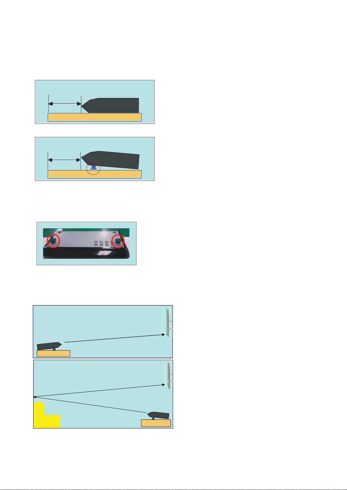
1. When setting up Media-Box at the cabinet and on th surface, etc
(1) If the surface distance becomes more than 20cm at [fig. 1],
wireless connection difficulty could be happened.
(2) Set up Media-Box making the surface distance as less than
20cm as possible.
(3) If the surface distance becomes more than 20cm unavoidably at
[fig. 2], a noise could be generated on the screen due to the drop
of wireless connection sensitivity.
(4) Improve wireless connection sensitivity by raising a wireless
emission angle using rubber (providing accessory).
2. When setting up Media-Box and TV, facing each other
If the surface distance on which Media-Box is placed becomes more than
20cm, wireless connection sensitivity could be dropped, and it is
recommended to use rubber.
3. In case setting up by using a reflection
The whole reflected distance shouldn’t be over 10m, and if
using a rubber according to the condition how Media-Box is
placed, wireless connection sensitivity improves. (a+b
distance should be smaller than 10m.)
- 14 -
Copyright © 2009 LG Electronics. Inc. All right reserved.
Only for training and service purposes
LGE Internal Use Only
MEDIA-BOX SETUP GUIDE
Surface Distance
More than 20cm
a
b
Sofa
[Fig. 3] Attach rubber to the lower part of Media-Box.
Page 15
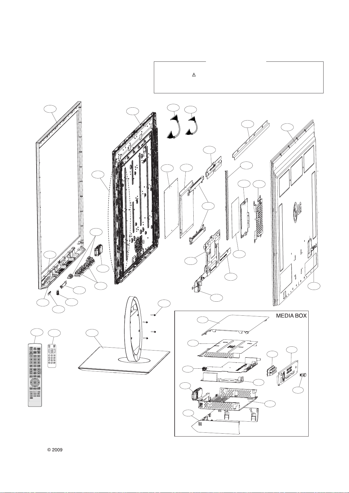
- 15 -
Copyright LG Electronics. Inc. All right reserved.
Only for training and service purposes
LGE Internal Use Only
300
200
200N
501
510
511
900
A10
531
530
400
800
801
802
541
540
542
803
550
500
310
120
121
590
532
700
710
770
780
790
720
730
750
740
760
804
543
A2
A22
LV1
LV2
Many electrical and mechanical parts in this chassis have special safety-related characteristics. These
parts are identified by in the Schematic Diagram and EXPLODED VIEW.
It is essential that these special safety parts should be replaced with the same components as
recommended in this manual to prevent X-RADIATION, Shock, Fire, or other Hazards.
Do not modify the original design without permission of manufacturer.
IMPORTANT SAFETY NOTICE
EXPLODED VIEW
Page 16
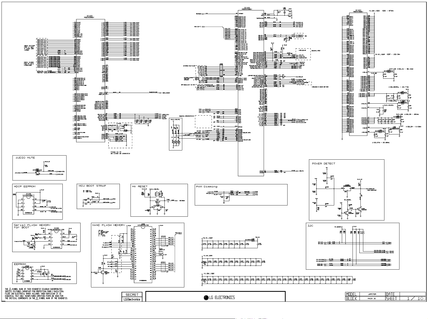
Copyright © 2009 LG Electronics. Inc. All right reserved.
Only for training and service purposes
LGE Internal Use Only
Page 17

Copyright © 2009 LG Electronics. Inc. All right reserved.
Only for training and service purposes
LGE Internal Use Only
Page 18

Copyright © 2009 LG Electronics. Inc. All right reserved.
Only for training and service purposes
LGE Internal Use Only
Page 19

Copyright © 2009 LG Electronics. Inc. All right reserved.
Only for training and service purposes
LGE Internal Use Only
Page 20

Copyright © 2009 LG Electronics. Inc. All right reserved.
Only for training and service purposes
LGE Internal Use Only
Page 21

Copyright © 2009 LG Electronics. Inc. All right reserved.
Only for training and service purposes
LGE Internal Use Only
Page 22

Copyright © 2009 LG Electronics. Inc. All right reserved.
Only for training and service purposes
LGE Internal Use Only
Page 23

Copyright © 2009 LG Electronics. Inc. All right reserved.
Only for training and service purposes
LGE Internal Use Only
Page 24
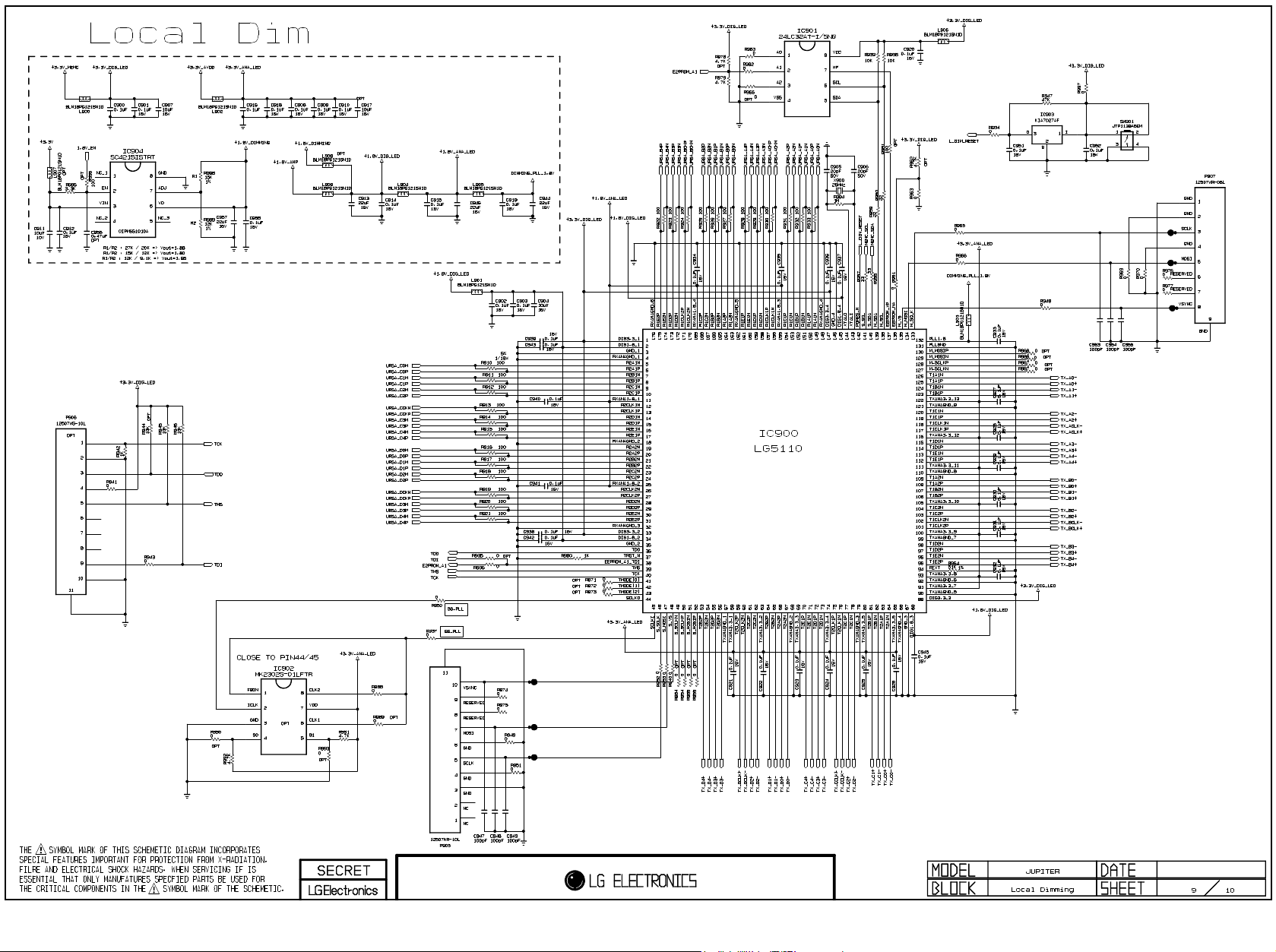
Copyright © 2009 LG Electronics. Inc. All right reserved.
Only for training and service purposes
LGE Internal Use Only
Page 25
Copyright © 2009 LG Electronics. Inc. All right reserved.
Only for training and service purposes
LGE Internal Use Only
Page 26
A CB
Copyright © 2009 LG Electronics. Inc. All right reserved.
Only for training and service purposes
LGE Internal Use Only
ANALOG IN/OUT
1
2
3
4
5
JACK TO MAIN WAFER
P1200
10022HS-31A02
1
2
3
4
5
6
7
8
9
10
11
12
13
14
15
16
17
18
19
20
21
22
23
24
25
26
27
28
29
30
31
COMP1_Y
COMP2_Y
COMP1_PB
COMP2_PB
COMP1_PR
COMP2_PR
COMP1_AUDIO_L
COMP2_AUDIO_L
COMP1_AUDIO_R
COMP2_AUDIO_R
AV1_Y_IN
AV1_C_IN
AV1_CVBS_IN
AV2_CVBS_IN
AV1_AUDIO_L
AV2_AUDIO_L
AV1_AUDIO_R
AV2_AUDIO_R
RS-232 Serial Port
C1129
0.33uF
16V
C1105 0.1uF
C1106 0.1uF
C1107 0.1uF
C1108 0.1uF
IC1103
MAX3232CDR
C1+
1
16V
V+
2
16V
C1-
3
C2+
4
16V
C2-
5
V-
6
16V
DOUT2
7
RIN2
8
VCC
16
GND
15
DOUT1
14
RIN1
13
1mA
ROUT1
12
DIN1
11
DIN2
10
ROUT2
9
R1131
100
R1132
100
009:B3
009:B4
009:B3
009:B4
009:B3
009:B4
001:D2
001:D3
001:D2
001:D3
009:B4
009:B4
001:C3;009:B4
001:C3;009:B4
001:D1
001:D1
001:D1
001:D2
4.7K
4.7K
R1120
R1117
R1115 0
R1116 0
R1113 100
R1114 100
In case of 2Vrms INPUT, Voltage divider for Mstar(3.3Vp-p ADC) * PC sound input & AV audio input voltage divider value is different so we need cordinate it in next model
D3.3V_2
R1237
4.7K
R1240 1K
D3.3V_2
R1277
4.7K
R1283 1K
D3.3V_2
R1204
4.7K
SYS_UART_RXD
SYS_UART_TXD
R1056
4.7K
220pF
C1114
C1252
47pF
50V
C1227
47pF
50V
C1229
47pF
50V
C1230
47pF
50V
50V
R1212 1K
R1060 1K
D3.3V_2
R1248
4.7K
AV1_CVBS_IN
AV2_CVBS_IN
AV1_Y_IN
AV1_C_IN
D3.3V_L
014:C5;014:F5
014:F5
220pF
C1115
50V
D3.3V_2
L1103 BLM18PG121SN1D
C1112
0.1uF
16V
OPT
OPT
6
THE SYMBOL MARK OF THIS SCHEMETIC DIAGRAM INCORPORATES
SPECIAL FEATURES IMPORTANT FOR PROTECTION FROM X-RADIATION.
FILRE AND ELECTRICAL SHOCK HAZARDS, WHEN SERVICING IF IS
ESSENTIAL THAT ONLY MANUFATURES SPECFIED PARTS BE USED FOR
THE CRITICAL COMPONENTS IN THE SYMBOL MARK OF THE SCHEMETIC.
AV1_SVIDEO_DET
R1254 1K
001:B2;009:B4
001:B2;009:B4
OPT
AV1_CVBS_DET
AV2_CVBS_DET
001:B2;009:B4
001:B2;009:B4
D1101
ADUC30S03010L
COMP1_DET
COMP2_DET
OPT
001:B3;009:I4
009:F5
C1130
47pF
50V
D1102
ADUC30S03010L
001:B2;009:I4
001:B2;009:I4
001:B3;009:I4
TXD
RXD
C1131
47pF
50V
R1133
220
R1134
220
001:B2
GND_CONTACT
R_CONTACT
T_CONTACT
SWITCH_A
SWITCH_B
SWITCH_C
SWITCH_F
SWITCH_E
001:B3
001:B3
001:B3
001:B3
001:B2
001:B2
001:B2
AV1_AUDIO_L
AV1_AUDIO_R
AV2_AUDIO_L
AV2_AUDIO_R
COMP1_AUDIO_L
COMP1_AUDIO_R
COMP2_AUDIO_L
COMP2_AUDIO_R
J1100
KJA-PH-1-0107
5
1
4
6
SHIELD
R1211 10K
R1205 10K
R125 9 1 0K
R125 8
R1252 10K
R1251 10K
R129 2 1 0K
R129 1 1 0K
AV1_L_IN
R1210
C1251
12K
1000pF
50V
AV1_R_IN
R1207
C1250
12K
1000pF
50V
Lowpass filter Fc=29Khz
AV2_L_IN
R1264
C1224
12K
1000pF
50V
10K
AV2_R_IN
C1243
R1263
1000pF
12K
50V
COMP1_L_IN
R1256
12K
COMP1_R_IN
C1221
R1255
1000pF
12K
50V
COMP2_L_IN
C1237
R1294
1000pF
12K
50V
COMP2_R_IN
C1238
R1293
1000pF
12K
50V
C1225
1000pF
50V
009:D3
009:D3
009:D3
009:D3
009:D3
009:D3
009:D3
009:D3
F
RGB PC
009:B3
009:B3
009:B3
009:B3
009:B3
DSUB_VSYNC
DSUB_HSYNC
DSUB_B
C1231
68pF
DSUB_G
DSUB_R
C1232
68pF
R1232 68
R1233 68
R1234
75
R1235
75
R1236
75
AT24C02BN-10SU-1.8
A0
1
A1
2
A2
3
GND
4
IC1200
8
7
2mA
6
5
D1207
ADUC30S03010L
C1216
OPT
C1217
OPT
C1218
OPT
VCC
WP
SCL
SDA
D1217
ADUC30S03010L
D1218
ADUC30S03010L
D1219
ADUC30S03010L
GD
C1222
18pF
50V
D1216
ADUC30S03010L
R1249
R1253
4.7K
4.7K
C1223
18pF
50V
R1257
22
111213
6
7
1
2
JK1201
KCN-DS-3-0054
D1223
ENKMC2838-T112
C
R1262
10K
R1269
D1222
ADMC5M03200L
OPT
8
9
3
A1
A2
100
14
4
C1228
0.1uF
16V
HE
D5.0V_VGA
P5.0V_ST
009:I5
VGA_EEPROM_WP
009:A6;009:F4
ISP_RXD
ISP_TXD
R1238 0
R1239 0
R1265
22
D1224
ADMC5M03200L
OPT
D5.0V_1
R1270
10K
R1271 1K
D1225
ADMC5M03200L
OPT
R1268 0
OPT
15
16
10
5
RGB_DDC_SCL
RGB_DDC_SDA
D5.0V_VGA
C1226
0.1uF
16V
009:A6;009:F4
012:F3
012:F3
DSUB_DET
PC AUDIO
JK1205
KJA-PH-1-0107
GND_CONTACT
5
R_CONTACT
1
T_CONTACT
4
SWITCH_A
SWITCH_B
A
B
SWITCH_C
C
D SWITCH_D
SWITCH_F
F
E
SWITCH_E
6
SHIELD
A
B
C
DSWITCH_D
F
E
SPDIF OPTIC JACK
NAND GATE FOR INVERTING
SPDIF_OUT
017:A2;009:E3
R1381
4.7K
A
B
GND
NL17SZ00DFT2G
1
2
3
In case of 2Vrms INPUT, Voltage divider for Mstar(3.3Vp-p ADC)
IC1203
R1382
D1234
ADMC5M03200L
OPT
D1235
ADMC5M03200L
OPT
D3.3V_2
VCC
5
C1255
0.1uF
50V
Y
4
0
OPT
R1383
22
1/10W
1%
D3.3V_2
OPT
R1297
470K
R1298
470K
JUNO-BOX
IN/OUT
R1300
15K
R1301
15K
Lowpass filter Fc=22Khz
R1384
0
R638
1K
OPT
C1254
D610
100pF
50V
R1303
10K
R1304
10K
D5.0V_1
R1385
C660
0.1uF
50V
R1305 0
PC_R_IN
009:D3
C1240
100pF
50V
R1307 0
PC_L_IN
009:D3
C1241
100pF
50V
Fiber Optic
0
OPT
GND
1
VCC
2
JK1206
JST1224
VIN
3
09.02.16
01 17
Page 27
BA
Copyright © 2009 LG Electronics. Inc. All right reserved.
Only for training and service purposes
LGE Internal Use Only
5V_HDMI_3
BODY_SHIELD
20
JK502
YKF45-7059V
BODY_SHIELDGND
20
JK501
YKF45-7059V
GND
20
JK503
YKF45-7059V
HP_DET
19
5V
18
GND
17
DDC_DATA
16
DDC_CLK
15
NC
14
CE_REMOTE
13
CK-
12
CK_GND
11
CK+
10
D0-
9
D0_GND
8
D0+
7
D1-
6
D1_GND
5
D1+
4
D2-
3
D2_GND
2
D2+
1
HP_DET
19
5V
18
GND
17
DDC_DATA
16
DDC_CLK
15
NC
14
CE_REMOTE
13
CK-
12
CK_GND
11
CK+
10
D0-
9
D0_GND
8
D0+
7
D1-
6
D1_GND
5
D1+
4
D2-
3
D2_GND
2
D2+
1
HP_DET
19
5V
18
GND
17
DDC_DATA
16
DDC_CLK
15
NC
14
CE_REMOTE
13
CK-
12
CK_GND
11
CK+
10
D0-
9
D0_GND
8
D0+
7
D1-
6
D1_GND
5
D1+
4
D2-
3
D2_GND
2
D2+
1
GND
5V_HDMI_2
GND
5V_HDMI_4
GND
R501 3.6K
R502 3.6K
OPT
R518 3.6K
R522
OPT
VR500
AVRL161A1R1NT
VR501
OPT
AVRL161A1R1NT
OPT
R1506
1K
OPT
VR506
AVRL161A1R1NT
OPT
OPT
OPT
1K
R1501
C501
0.1uF
16V
R510 0
R511
R509 0
R590 0
R585 0
R591 0
R586 0
R587 0
R592 0
R588
R589 0
OPT
C502
1K
0.1uF
16V
OPT
R506 0
R507 0
R508 0
R569
R570
R571
R572
R573
R574
R575
R576
R519
OPT
VR507
AVRL161A1R1NT
C505
0.1uF
OPT
16V
R524 0
R523 0
R525
R594
R593
R595
R596
R597
R598
R599
R526
1
2
3
4
5
6
THE SYMBOL MARK OF THIS SCHEMETIC DIAGRAM INCORPORATES
SPECIAL FEATURES IMPORTANT FOR PROTECTION FROM X-RADIATION.
FILRE AND ELECTRICAL SHOCK HAZARDS, WHEN SERVICING IF IS
ESSENTIAL THAT ONLY MANUFATURES SPECFIED PARTS BE USED FOR
THE CRITICAL COMPONENTS IN THE SYMBOL MARK OF THE SCHEMETIC.
D3.3V_2
R1500
47K
OPT
0
R513
OPT
VR503
AVRL161A1R1NT
OPT
R516 1K
OPT
0
002:B3;002:B5;002:D1;002:E1;002:H5
0
HDMI_PORT3
D3.3V_2
R1503
47K
R514
OPT
0
OPT
VR504
OPT
R517 1K
AVRL161A1R1NT
002:B1;002:B5;002:D1;002:E1;002:H5
0
0
0
0
0
0
0
0
HDMI_PORT2
D3.3V_2
R1507
OPT
47K
0
HPD4
002:G3
R521
1K
OPT
0
002:B1;002:B3;002:D1;002:E1;002:H5
0
0
0
0
0
0
0
0
HDMI_PORT4
JP506
JP507
JP505
002:F6
JP502
JP503
002:C4;002:G6
002:C4;002:G6
002:G6
002:G6
002:G6
002:G6
002:G6
002:G6
002:G6
002:G6
002:H5
JP504
002:D3;002:H4
002:D3;002:H4
002:H4
002:H4
002:H4
002:H4
002:H4
002:H4
002:H4
002:H4
002:D4;002:G3
002:D4;002:G3
002:G3
002:G3
002:G3
002:G3
002:G3
002:G3
002:G3
002:G3
HPD3
DDC_SDA_3
DDC_SCL_3
CEC_REMOTE
CK-_HDMI3
CK+_HDMI3
D0-_HDMI3
D0+_HDMI3
D1-_HDMI3
D1+_HDMI3
D2-_HDMI3
D2+_HDMI3
HPD2
DDC_SDA_2
DDC_SCL_2
CEC_REMOTE
CK-_HDMI2
CK+_HDMI2
D0-_HDMI2
D0+_HDMI2
D1-_HDMI2
D1+_HDMI2
D2-_HDMI2
D2+_HDMI2
DDC_SDA_4
DDC_SCL_4
CEC_REMOTE
CK-_HDMI4
CK+_HDMI4
D0-_HDMI4
D0+_HDMI4
D1-_HDMI4
D1+_HDMI4
D2-_HDMI4
D2+_HDMI4
GND
20
19
18
17
16
15
14
13
12
11
10
9
8
7
6
5
4
3
2
1
JK500
KJA-ET-0-0032
5V_HDMI_1
R533 R545
R534
47K
5V_HDMI_3
R536
IF HDMI 15M TEST FAIL, CHANGE 47K PULL UP RESISTOR VALUE TO 4.7K
VARISTORS(VR500/501/502/503/504/505/506/507) on lines-HPD1/2/3/4 are all options
in case HDMI Switch doesn’t support ’ESD protection’
5V_HDMI_1
R500 3.6K
OPT
R1504
1K
OPT
OPT
VR502
R503 0
R504 0
AVRL161A1R1NT
R505
R577 0
R579
R580
R581 0
R578
R582
R583
R584
FRONT_HDMI_PORT1
DDC_SDA_1
DDC_SCL_1
DDC_SDA_3
DDC_SCL_3
C500
0.1uF
16V
OPT
0
5V_HDMI_2
5V_HDMI_4
HP_DET
5V
GND
DDC_DATA
DDC_CLK
NC
CE_REMOTE
CK-
CK_GND
CK+
D0-
D0_GND
D0+
D1-
D1_GND
D1+
D2-
D2_GND
D2+
GND
R535
47K
R538
R537
47K R559
47K
D E H
D3.3V_2
R1505
R512
47K
0
OPT
OPT
VR505
OPT
R515 1K
AVRL161A1R1NT
JP500
JP501
002:C3;002:E4
002:B1;002:B3;002:B5;002:E1;002:H5
0
0
0
0
0
0
R547
R546
47K
47K
R558
R561
47K
47K
EDID Pull-up
* HDMI CEC
Protect reverse current from external device to TV set When Set Power off
002:F4
HPD1
DDC_SDA_1
002:C3;002:E4
DDC_SCL_1
CEC_REMOTE
CK-_HDMI1
002:F4
CK+_HDMI1
002:F4
D0-_HDMI1
002:F4
D0+_HDMI1
002:F4
D1-_HDMI1
002:F5
D1+_HDMI1
002:F5
D2-_HDMI1
002:F5
D2+_HDMI1
002:F5
DDC_SDA_2
DDC_SCL_2
DDC_SDA_4
DDC_SCL_4
002:B1;002:B3;002:B5;002:D1;002:H5
CEC_REMOTE
0
GND
DDC_SDA_1
DDC_SCL_1
HDMI 1
For Only TDA9996 ES3
R520
VR508
AVRL161A1R1NT
D3.3V_HDMI
The Value is nedd to be adjustable for External Load in case of HDMI regualtion test
DRAIN1
GATE2
SOURCE2
6
5
4
0
SSM6N15FU
OPT
D500
MMBD301LT1G
HDMI INPUT
P5.0V_ST
OPT
R540 0
R539 0
2K
R542
R541 2K
5V_HDMI_1
C509
0.1uF
16V
HPD1
CK-_HDMI1
CK+_HDMI1
D0-_HDMI1
D0+_HDMI1
D1-_HDMI1
D1+_HDMI1
D2-_HDMI1
D2+_HDMI1
P5.0V_ST
R543
C507
0.1uF
D1.8V_HDMI
C508
C506
0.1uF
0.1uF
16V
16V
FC
D3.3V_2
R52868K
IC501
R529 9.1K
0.1uF
HDMI_CEC_RX
012:C3;009:B3
C503
16V
GND
SOURCE1
1
GATE1
2
DRAIN2
3
R527
D3.3V_HDMI
R544
0
G
D1.8V_1
CB3216PA501E
HDMI 4
C515 0.1uF
C513 0.1uF
C514 0.1uF
0
C510
0.1uF
16V
HDMI_SCL
HDMI_SDA
HDMI_CLK-
HDMI_CLK+
HDMI_RX0-
OUT_DDC_CLK
OUT_DDC_DAT
VDDC[1V8]_1
RXA_DDC_DAT
RXA_DDC_CLK
VDDH[3V3]_1
VDDH[3V3]_2
VDDH[1V8]_1
C511 0.1uF
HDMI_RX1-
HDMI_RX1+
HDMI_RX0+
VSS_1
OUT_C+
OUT_C-
VDDO[3V3]
VSS_2
RXA_HPD
RXA_5V
RXA_CRXA_C+
RXA_D0RXA_D0+
VSS_3
RXA_D1RXA_D1+
RXA_D2RXA_D2+
NC
5V_HDMI_3
Net Labels changed for HDMI3
HDMI_RX2+
HDMI_RX2-
OUT_D0-
100
1
2
3
4
5
6
7
8
9
10
11
12
13
14
15
16
17
18
19
20
21
22
23
24
25
26
VSS_4
C512
0.1uF
16V
27
28
TEST
RXB_HPD
29
30
RXB_5V
RXB_DDC_DAT31RXB_DDC_CLK
HPD3
DDC_SDA_3
C516 0.1uF
C517 0.1uF
D2-_HDMI4
D2+_HDMI4
RXD_D2-90RXD_D2+91VDDC[1V8]_3
VSS_1193OUT_D2+94OUT_D2-95VDDO[1V8]96OUT_D1+97OUT_D1-98VSS_1299OUT_D0+
89
92
IC502
TDA9996HL
1.8V: 346mA
3.3V: 59mA
32
34
35
37
VSS_5
RXB_C-33RXB_C+
RXB_D0-36RXB_D0+
VDDH[3V3]_3
DDC_SCL_3
D0-_HDMI3
CK+_HDMI3
CK-_HDMI3
D0+_HDMI3
HDMI 3
D1+_HDMI4
NEW
38
RXB_D1-39RXB_D1+
D1-_HDMI3
D1-_HDMI4
40
41
RXB_D2-42RXB_D2+
VDDH[3V3]_4
D2-_HDMI3
D1+_HDMI3
D0-_HDMI4
D0+_HDMI4
RXD_D0-84RXD_D0+85VSS_1086RXD_D1-87RXD_D1+88VDDH[3V3]_8
83
43
44
VSS_6
CDEC_DDC
D2+_HDMI3
CK+_HDMI4
CK-_HDMI4
RXD_DDC_CLK
RXD_DC-81RXD_DC+82VDDH[3V3]_7
79
80
45
46
47
MODE
VDDC[3V3]
VDDC[1V8]_2
R548 0
R549
DDC_SDA_4
DDC_SCL_4
48PD49
SDA/SEL150SCL/SEL0
R550 0
TDA9996_SDA
HPD4
5V_HDMI_4
RXD_HPD77RXD_5V78RXD_DDC_DAT
76
75
74
73
72
71
70
69
68
67
66
65
64
63
62
61
60
59
58
57
56
55
54
53
52
51
R551 0
R552
OPT
R553
OPT
R554
OPT
TDA9996_SCL
JUNO-BOX
HDMI SW
D1.8V_HDMI
L500
C518
0.1uF
16V
VDDH[1V8]_2
R12K
VSS_9
RXC_D2+
RXC_D2VDDH[3V3]_6
RXC_D1+
RXC_D1VSS_8
RXC_D0+
RXC_D0VDDH[3V3]_5
RXC_C+
RXC_CRXC_DDC_CLK
RXC_DDCC_DAT
RXC_5V
RXC_HPD
CEC
VSS_7
VDDS[3V3]
CDEC_STBY
INT/HP_CTRL
XTAL_OUT
XTAL_IN
R555
OPT
C519
0.1uF
16V
D3.3V_HDMI
4.7K
C530
0.1uF
R556
12K
0.1uF
C521
0
C520
0.1uF
16V
C522
0.1uF
16V
5V_HDMI_2
R557
0
R560 0
HDMI S/W 4:1
D3.3V_HDMI
D3.3V_2
L501
BLM18PG121SN1D
C525 0.1uF
C526
C527
C528
D1.8V_HDMI
C524
0.1uF
16V
C523
0.1uF
16V
Net Labels changed for HDMI2
OPT
0.1uF
0.1uF
0.1uF
C529
0.1uF
16V
D2+_HDMI2
D2-_HDMI2
D1+_HDMI2
D1-_HDMI2
D0+_HDMI2
D0-_HDMI2
CK+_HDMI2
CK-_HDMI2
DDC_SCL_2
DDC_SDA_2
HPD2
CEC_REMOTE
C504
0.1uF
Mode 47Pin Low(I2C-bus mode)
02 17
HDMI 2
Page 28
A
Copyright © 2009 LG Electronics. Inc. All right reserved.
Only for training and service purposes
LGE Internal Use Only
B
POWER SUPPLY
C
D E
F
G
H
POWER CONNECTOR
1
C700
0.1uF
16V
C701
0.1uF
16V
C702
C703
100uF
16V
100uF
16V
P3.3V
P6.0V
+6.0V
+6.0V
+3.3V
+5.0V_ST
+5.0V_ST
GND
GND
GND
P700
SMW250-16P
2
4
6
8
10
12
14
16
P5.0V_ST
PWR_CTRL
1
+6.0V
3
GND
5
+3.3V
7
GND
9
+5.0V_ST
11
GND
13
GND
15
OPT
OPT
2
3
L703
BLM18PG121SN1D
P6.0V
L704
CB3216UA121
L705
CB3216UA121
D705
ENKMC2838-T112
A1
A2
C729
10pF
50V
D3.3V_AVDD_MPLL
C717
0.1uF
16V
C
D3.3V_2
IC706
NEW
3IN1
2
OUT
C734
4.7uF
6.3V
ADJ/GND
R706 1K
C735
47uF
16V
C731
C730
0.01uF
0.1uF
50V
16V
Replaced Part
AP1117E33G-13
C753
C752
0.1uF
10uF
16V
10V
4
5
P3.3V
D3.3V_1
+3.3V For TMDS Switch
+5.0V_ST 2A
+6.0V 2.9A
+3.3V 1.5A
R700
1K
PWR_CTRL
C709
100uF
16V
012:F3
C706
10uF
16V
C707
0.1uF
16V
+5.0V For USB & Etc +1.8V For HDMI TX
P6.0V
C711
100uF
16V
C716
0.1uF
16V
VCC
R701
1K
BA50BC0WFP-E2
2
1
CTL
GND
IC700
D5.0V_1
OUT
4
3
5
C719
NC
C718
100uF
16V
0.1uF
16V
D3.3V_2 D1.8V_1
C723
47uF
16V
C724
0.1uF
16V
IC703
AP1117E18G-13
NEW
3IN1
2
OUT
C725
47uF
16V
ADJ/GND
C726
0.1uF
16V
+1.26 Core for Saturn6
P6.0V
465 mA @85% efficiency
D3.3V_1
MAX 3A
R738
10K
Close to IC
R736 22K
EN/SYNC
8
SW_2
7
SW_1
6
VCC
5
C790
0.1uF
16V
1%
R742 10
If there is problem about DCDC BS, then change to R742 0ohm
C788
1uF
16V
OPT
$0.07
4.9A 0.0150OHM 34MHZ
L726
3.6uH
NR8040T3R6N
C789
0.1uF
50V
C OUT
C791
22uF
16V
D1.26V_VDDC
1600 mA
3A, DCR=0.025 ohm
L717
BLM18PG121SN1D
C792
22uF
16V
Placed on SMD-TOP
0.1uF
C793
D701
SML-201MT
L711
CB3216PA501E
Placed on SMD-TOP
C787
C786
22uF
22uF
OPT
C IN
Vout=0.8*(1+R1/R2)
Close to IC
R723
22K
R1
1%
R722
75K
R2
1%
OPT
D703
100V
1N4148W_DIODES
FB
GND
IN
BS
Replaced Part
R731 10K
IC705
MP2212DN
1
NEW
2
$0.24
3
4
R724 10
OPT
1%
+1.8V for Saturn6 DDR
D3.3V_1
BLM18PG121SN1D
L702
R710
10K
D3.3V_3
C754
C755
10uF
0.1uF
6.3V
16V
C712
C713
10uF
0.1uF
10V
16V
IC701
SC4215ISTRT
NC_1
EN
VIN
NC_2
R1/R2 : 27K / 20K => Vout=1.88
R1/R2 : 15K / 12K => Vout=1.80
R1/R2 : 12K / 9.1K => Vout=1.85
GND
1
8
ADJ
2
7
VO
3
6
NC_3
4
5
D1.8V_DDR
R711
12K
1%
C714
R712
9.1K
1%
C715
22uF
0.1uF
16V
16V
Stand-by +3.3V
P5.0V_ST
L724
CB3216PA501E
Replaced Part
IC702
AP1117E33G-13
ADJ/GND
NEW
3IN1
C705
0.1uF
16V
2
OUT
C704
10uF
10V
+3.3V
P6.0V
L716
CB3216PA501E
C733
C732
22uF
22uF
16V
Placed on SMD-TOP
Vout=0.8*(1+R1/R2)
R1
R2
OPT
Close to IC
R770
56K
1%
R769
18K
1%
D700
OPT
100V
1N4148W_DIODES
FB
GND
IN
BS
OPT
R733 10K
IC704
MP2212DN
1
NEW
95% Efficiency
2
3
4
R734
10
1/10W
1%
GND
Switch for +5.0V (WIRELESS)
P5.0V_ST
012:F2
WIHD_PWR_EN
R703 10K
R702
120K
B
R704
47K
R705
2.7K
C
E
8
7
6
5
Q700
2SC3052
D3.3V_L
R772 4.7K
C708
C710
10uF
0.1uF
6.3V
16V
012:F3
D3.3V_EN
R756 100
EN/SYNC
SW_2
SW_1
VCC
CB3216UA121
R771
GND
C741
0.1uF
50V
R737
10
C737
1uF
10V
If there is problem about DCDC BS, then change to R742 0ohm
GND
D5.0V_W
L700
OPT
C720
10uF
OPT
C721
0.1uF
16V
C722
8.0PI
OPT
3.9K
L710
3.6uH
NR8040T3R6N
D704
SML-512UW
PV
D3.3V_1
C751
10uF
6.3V
GND
L720
BLM18PG121SN1D
C746
0.1uF
L701
CB3216UA121
Q701
SI4925BDY
1S1
2G1
3S2
4G2
8 D1_2
7 D1_1
6 D2_2
5 D2_1
BLM18PG121SN1D
C750
22uF
16V
GNDGND
L727
C780
OPT
0.1uF
16V
6
THE SYMBOL MARK OF THIS SCHEMETIC DIAGRAM INCORPORATES
SPECIAL FEATURES IMPORTANT FOR PROTECTION FROM X-RADIATION.
FILRE AND ELECTRICAL SHOCK HAZARDS, WHEN SERVICING IF IS
ESSENTIAL THAT ONLY MANUFATURES SPECFIED PARTS BE USED FOR
THE CRITICAL COMPONENTS IN THE SYMBOL MARK OF THE SCHEMETIC.
AN SO YOUNG
JUNO-BOX
POWER 04 17
Page 29
DEMODULATOR LGDT3900
Copyright © 2009 LG Electronics. Inc. All right reserved.
Only for training and service purposes
LGE Internal Use Only
+3.3V_DTMB
C1005
C1010
C1018
C1016
10uF
0.1uF
0.1uF
0.1uF
10V
16V
16V
C1017
C1013
C1007
TU_IF_OUT-
009:AT3
TU_IF_OUT+
009:AT4
R1000
R1002
0
TU_IF_AGC
P6.0V
009:AQ7
1K
1/16W
C1002
5%
0.1uF
16V
TU_SCL_3.3V
009:K13
TU_SDA_3.3V
009:S12
+3.3V_DTMB
R1001
100
FIN must be connected GND
VCC
C1000
C1001
47uF
0.1uF
16V
50V
P6.0V
+3.3V_DTMB
C1003
0.1uF
16V
THE SYMBOL MARK OF THIS SCHEMETIC DIAGRAM INCORPORATES
SPECIAL FEATURES IMPORTANT FOR PROTECTION FROM X-RADIATION.
FILRE AND ELECTRICAL SHOCK HAZARDS, WHEN SERVICING IF IS
ESSENTIAL THAT ONLY MANUFATURES SPECFIED PARTS BE USED FOR
THE CRITICAL COMPONENTS IN THE SYMBOL MARK OF THE SCHEMETIC.
0.1uF
0.1uF
10uF
16V
10V
C1014
C1015
Close to IC
R1003
1K
1/16W
5%
C1006
0.1uF
16V
+3.3V_DTMB
R1005
R1004
4.7K
4.7K
OPT
OPT
009:G20
009:G21
FE_DEMOD_SCL
001:D21
FE_DEMOD_SDA
001:D21
001:X26
A1[RD]
C
A2[GN]
LDPC ERR
LD1200
SAM2333
R1006
200
A1[RD]
C
A2[GN]
LOCK
LD1201
SAM2333
IC1000
BA50BC0WFP-E2
2
4
1
3
5
NC
CTL
GND
+3.3V/+1.2V_DTMB
C1011
C1008
0.1uF
100uF
16V
16V
C1009
C1012
0.1uF
100uF
16V
16V
IC1002
SC4215ISTRT
NC_1
1
EN
2
C1004
VIN
3
10uF
10V
NC_2
4
16V
SYNCLOCK
/FE_RESET
OUT
16V
0.01uF25V
0.01uF25V
+3.3V_DTMB
BLKERR
C1033
C1029
C1022
0.1uF
0.1uF
0.1uF
16V
16V
16V
+1.2V_DTMB
C1021
C1028
C1032
16V
0.1uF
R1007
4.7K
R1008 100
R1009 100
BLKERR
SYNCLOCK
C1038
0.1uF
0.1uF
16V
16V
16V
+3.3VA_DTMB
C1034
0.1uF
0.1uF
16V
16V
C1023
1uF
OPT
R1010
100
C1025
C1035
22pF
22pF
50V
50V
R1011
100
C1036
C1026
22pF
22pF
50V
50V
R1012
100
C1027
C1037
22pF
22pF
50V
50V
009:H27
009:H27
0.1uF
C1019
0.1uF
16V
C1020
0.1uF
16V
+5V_TUNER
+5V_TUNER
C1031
C1024
100uF
4.7uF
16V
10V
IC1001
KIA78R033F
VIN
1
VC
2
VOUT
3
NC
4
GND1
5
GND
8
ADJ
7
VO
6
NC_3
5
+1.2V_DTMB
R1014
5.1K
C1040
R1013
0.1uF
10K
16V
No more production TXC, China local cyristal will be used at MP
C1041
0.1uF
16V
CMDC
AVDD33_1
AVSS_1
AIFINN
AIFINP
VREFN
VREFP
AVDD33_2
AVSS_2
I2CSEL
AGCOUT
TUNSCL
TUNSDA
VSS_1
VDD_1
GPIO[5]
GPIO[4]
VDD33_1
GPIO[3]
GPIO[2]
VSS_2
GPIO[1]
GPIO[0]
LOCK
nERROR
C1039
0.1uF
50V
6
GND2
C1042
22uF
16V
C1045
C1043
18pF
X1005
18pF
30.4MHz
R1016
1M
R1015
R1017
470
470
VSS_11
100
1
2
3
4
5
6
7
8
IC1004
9
10
LG3900
11
12
13
14
15
16
17
18
19
20
360mmA
21
22
23
24
25
26
28
29
30
32
33
37
nRESET
P6.0V
TPVALID
TPDATA[0]31TPDATA[1]
VSS_3
L1000
CIC21J501NE
VDD33_2
TPDATA[2]34TPDATA[3]35TPDATA[4]36TPDATA[5]
C
C1044
100uF
16V
38
VDD_2
C1046
0.1uF
16V
SCL27SDA
39
TPDATA[6]40TPDATA[7]
INPUT
41
44
TPCLK42TPSOP43VSS_4
SADDR[3]45SADDR[2]46SADDR[1]47SADDR[0]
IC1003
AZ1117D-3.3TRE1
3
1
ADJ/GND
R1018
0
OUTPUT
2
VSS_877SDQ[9]78SDQ[8]79SCLK80SCKE81SADDR[9]82SADDR[8]83SADDR[7]84VDD33_585VSS_986SADDR[6]87SADDR[5]88VDD_589SADDR[4]90OPM[0]91OPM[1]92OPM[2]93TMOD94VSS_1095XTALI96XTALO97VDD33_698TESTSE99VDD_6
76
48
49
SBA[1]50SBA[0]
SADDR[10]
R1019 47
R1020 47
R1021 47
R1022 47
SDQ[10]
75
SDQ[11]
74
SDQ[12]
73
SDQ[13]
72
VSS_7
71
SDQ[14]
70
SDQ[15]
69
VDD33_4
68
VDD_4
67
SDQ[0]
66
SDQ[1]
65
SDQ[2]
64
VSS_6
63
SDQ[3]
62
SDQ[4]
61
SDQ[5]
60
VDD_3
59
SDQ[6]
58
SDQ[7]
57
nSWE
56
VDD33_3
55
nSCAS
54
nSRAS
53
VSS_5
52
nSCS
51
+3.3VA_DTMB
C1047
100uF
16V
C1048
4.7uF
10V
D
+3.3VA_DTMB
LGDT_SADDR[4]
LGDT_SADDR[5]
LGDT_SADDR[6]
LGDT_SADDR[7]
LGDT_SADDR[8]
LGDT_SADDR[9]
LGDT_SDQ[8]
LGDT_SDQ[9]
LGDT_SDQ[10]
LGDT_SDQ[11]
LGDT_SDQ[12]
LGDT_SDQ[13]
LGDT_SDQ[14]
LGDT_SDQ[15]
LGDT_SDQ[0]
LGDT_SDQ[1]
LGDT_SDQ[2]
LGDT_SDQ[3]
LGDT_SDQ[4]
LGDT_SDQ[5]
LGDT_SDQ[6]
LGDT_SDQ[7]
LGDT_SWE
LGDT_SCAS
LGDT_SRAS
LGDT_SCS
LGDT_SADDR[10]
LGDT_SADDR[0]
LGDT_SADDR[1]
LGDT_SADDR[2]
LGDT_SADDR[3]
C1049
0.1uF
16V
009:Y28
009:Y28
009:Y27
009:Y27
FE_TS_SYN
FE_TS_DATA_CLK
FE_TS_SERIAL
FE_TS_VAL_ERR
LGDT_SCKE
LGDT_SCLK
LGDT_SADDR[0-10]
LGDT_SDQ[0-15]
LGDT_SDQ[0-15]
LGDT_SADDR[0-10]
009:T28
009:T27
009:T27
009:T27
009:V24
009:V24
LGDT_SBA[0]
LGDT_SBA[1]
001:AL16
001:AL17
001:AL16
001:AL16
+3.3V_DTMB
009:AG27
LGDT_SWE
LGDT_SCAS
LGDT_SRAS
LGDT_SCS
LGDT_SBA[0]
LGDT_SBA[1]
009:Y27
009:Y27
009:AG28
LGDT_SDQ[0]
LGDT_SDQ[1]
LGDT_SDQ[2]
LGDT_SDQ[3]
LGDT_SDQ[4]
LGDT_SDQ[5]
LGDT_SDQ[6]
LGDT_SDQ[7]
LGDT_SADDR[10]
LGDT_SADDR[0]
LGDT_SADDR[1]
LGDT_SADDR[2]
LGDT_SADDR[3]
C1050
C1051
0.1uF
0.1uF
16V
16V
HYNIX 64MBIT
VDD1
1
DQ0
2
VDDQ1
3
DQ1
4
DQ2
5
VSSQ1
6
DQ3
7
DQ4
8
VDDQ2
9
DQ5
10
DQ6
11
VSSQ2
12
DQ7
13
VDD2
14
LDQM
15
WE
16
CAS
17
RAS
18
CS
19
BA0
20
BA1
21
A10/AP
22
A0
23
A1
24
A2
25
A3
26
VDD3
27
C1052
0.1uF
16V
IC1005
HY57V641620FTP
Max 170mA
Typ 120mA
C1054
C1053
0.1uF
0.1uF
16V
16V
54
53
52
51
50
49
48
47
46
45
44
43
42
41
40
39
38
37
36
35
34
33
32
31
30
29
28
TUNER TDFR-Z751D
RF_SWITCH_SEL
001:X25;002:P22
R1059
4.7K
T-TDFR_Z051D
270mA
T-TDFR_Z051D
TU1001
TDFR-Z051D
R1023 47
24
C1057
0.1uF
16V
CTR
1
G-SW
2
+B1
3
VTU
4
RF_AGC
5
+B2
6
NC_1
7
SIF
8
VIDEO_OUT
9
NC_2
10
NC_3
11
TU_IF
12
NC_4
13
GND
14
NC_5
15
NC_6
16
SDA
17
SCL
18
NC_7
19
IF_AGC
20
DIF_1
21
DIF_2
22
NC_8
23
SHIELD
0
R1024
R1025 0
Close to tuner
C1055
C1058
C1056
0.1uF
10uF
0.1uF
16V
10VC1030
16V
ELITE 64MBIT
IC1005-*1
M12L64164A-5TG
VSS_3
54
53
52
51
50
49
48
47
46
45
44
43
42
41
40
39
38
37
36
35
34
33
32
31
30
29
28
TU_SCL_3.3V009:F29
DQ15
VSSQ_4
DQ14
DQ13
VDDQ_4
DQ12
DQ11
VSSQ_3
DQ10
DQ9
VDDQ_3
DQ8
VSS_2
NC_2
UDQM
CLK
CKE
NC_1
A11
A9
A8
A7
A6
A5
A4
H
VSS_1
009:W36
009:W37
VDD_1
1
DQ0
2
VDDQ_1
3
DQ1
4
DQ2
5
VSSQ_1
6
DQ3
7
DQ4
8
VDDQ_2
9
DQ5
10
DQ6
11
VSSQ_2
12
DQ7
13
VDD_2
14
LDQM
15
WE
16
CAS
17
RAS
18
CS
19
A13
20
A12
21
A10/AP
22
A0
23
A1
24
A2
25
A3
26
VDD_3
27
VSS3
DQ15
LGDT_SDQ[15]
VSSQ4
LGDT_SDQ[14]
DQ14
DQ13
LGDT_SDQ[13]
VDDQ4
DQ12
LGDT_SDQ[12]
DQ11
LGDT_SDQ[11]
VSSQ3
DQ10
LGDT_SDQ[10]
DQ9
VDDQ3
DQ8
VSS2
NC2
UDQM
CLK
CKE
NC1
A11
A9
A8
A7
A6
A5
A4
VSS1
LGDT_SCLK
LGDT_SCKE
LGDT_SADDR[9]
LGDT_SADDR[8]
LGDT_SADDR[7]
LGDT_SADDR[6]
LGDT_SADDR[5]
LGDT_SADDR[4]
LGDT_SDQ[9]
LGDT_SDQ[8]
R1030
4.7K
TU_SDA_5V009:AQ7
+5V_TUNER
R1055
R1036
0
R1037
0
4.7K
TU_SCL_5V 009:AQ7
TU_SDA_3.3V 009:F29
+5V_TUNER
R1039
0
E
R1051
2SA1504S
Q1001
B
C
C1071
100uF
16V
OPT
FE_SIF
+5V_TUNER
2.2K
2SC3875S(ALY)
002:S17
R1040 0
OPT
C1072
0.1uF
16V
B
C
R1046
10K
Q1003
R1050
270
R1044
270
E
ISA1530AC1
Q1105
C
B
E
R1045
0
FE_BOOSTER_CTL
FE_VMAIN
C1073
220pF
CVBS LINE MUST BE LOCATED IN 1’ST LAYER
50V
OPT
001:AJ11
002:E23
R1038
OPT
C1070
0.01uF
009:D34
25V
C1069
R1035
0
0.01uF
25V
R1034
0
+5V_TUNER
L1001
MLB-201209-0120P-N2
C1059
C1061
0.1uF
220uF
16V
16V
C1064
0.1uF
16V
C1063
100pF 50V
R1027 47
R1028
C1062
C1060
47pF
47pF
50V
50V
R1026
0
CM2012FR22KT
CM2012FR22KT
47
L1002
220nH
C1066
24pF
C1065
24pF
L1003
220nH
L1004
MLB-201209-0120P-N2
C1067
220uF
16V
L1005
CM2012FR47KT
0.47uH
+5V_TUNER
TU_SDA_5V
TU_SCL_5V
TU_IF_AGC
+5V_TUNER
R1032
470
R1033
82
E
ISA1530AC1
Q1104
B
C
R1031
4.7K
R1029
0
OPT
009:K12
009:S13
009:C31
TU_IF_OUT+ 009:D34
C1068
39pF
50V
TU_IF_OUT-
ROUTE SYMMETRICALLY
TUNER
Page 30
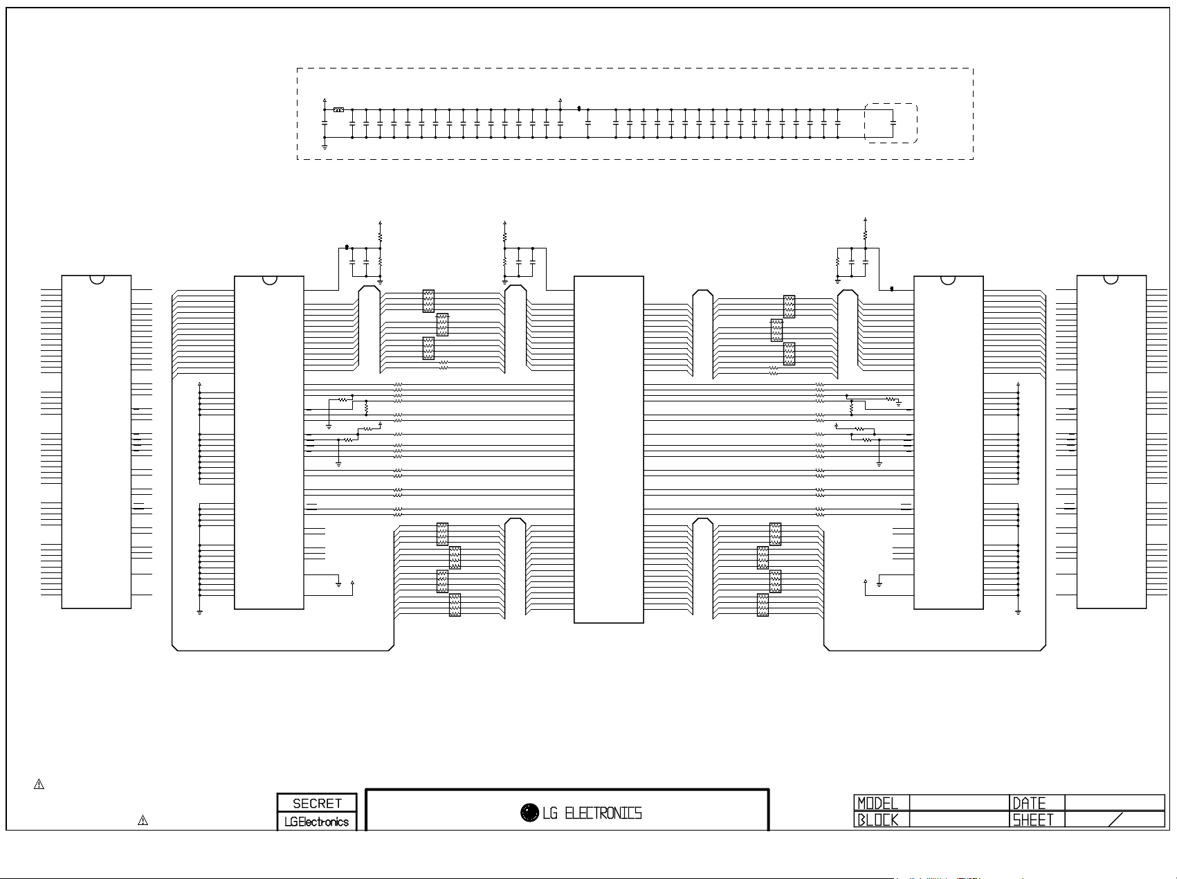
B
Copyright © 2009 LG Electronics. Inc. All right reserved.
Only for training and service purposes
LGE Internal Use Only
C
D E
FA
G
H
1
DDR2
2
Hynix
IC300-*1
HY5PS1G1631CFP-S6
DQ0
G8
DQ1
G2
DQ2
H7
DQ3
1GB
H3
DQ4
H1
Hynix
DQ5
H9
DQ6
F1
DQ7
F9
DQ8
C8
DQ9
C2
DQ10
D7
DQ11
D3
DQ12
VDDQ10
VDDQ9
VDDQ8
VDDQ7
VDDQ6
VDDQ5
VDDQ4
VDDQ3
VDDQ2
VDDQ1
VSSQ10
VSSQ9
VSSQ8
VSSQ7
VSSQ6
VSSQ5
VSSQ4
VSSQ3
VSSQ2
VSSQ1
D1
DQ13
D9
DQ14
B1
DQ15
B9
VDD5
A1
VDD4
E1
VDD3
J9
VDD2
M9
VDD1
R1
A9
C1
C3
C7
C9
E9
G1
G3
G7
G9
VSS5
A3
VSS4
E3
VSS3
J3
VSS2
N1
VSS1
P9
B2
B8
A7
D2
D8
E7
F2
F8
H2
H8
3
4
VREF
J2
A0
M8
A1
M3
A2
M7
A3
N2
A4
N8
A5
N3
A6
N7
A7
P2
A8
P8
A9
P3
A10/AP
M2
A11
P7
A12
R2
BA0
L2
BA1
L3
BA2
L1
CK
J8
CK
K8
CKE
K2
ODT
K9
CS
L8
RAS
K7
CAS
L7
WE
K3
LDQS
F7
UDQS
B7
LDM
F3
UDM
B3
LDQS
E8
UDQS
A8
NC5
R3
NC6
R7
NC1
A2
NC2
E2
NC3
R8
VSSDL
J7
VDDL
J1
SDDR_D[0]
SDDR_D[1]
SDDR_D[2]
SDDR_D[3]
SDDR_D[4]
SDDR_D[5]
SDDR_D[6]
SDDR_D[7]
SDDR_D[8]
SDDR_D[9]
SDDR_D[10]
SDDR_D[0-15]
SDDR_D[11]
SDDR_D[12]
SDDR_D[13]
SDDR_D[14]
SDDR_D[15]
D1.8V_S_DDR
VDDQ_10
VSSQ_10
EDE1116AEBG-8E-F
DQ0
G8
DQ1
G2
DQ2
H7
DQ3
H3
DQ4
H1
DQ5
H9
DQ6
F1
DQ7
F9
DQ8
C8
DQ9
C2
DQ10
D7
DQ11
D3
DQ12
D1
DQ13
D9
DQ14
B1
DQ15
B9
VDD_5
A1
VDD_4
E1
VDD_3
J9
VDD_2
M9
VDD_1
R1
A9
VDDQ_9
C1
VDDQ_8
C3
VDDQ_7
C7
VDDQ_6
C9
VDDQ_5
E9
VDDQ_4
G1
VDDQ_3
G3
VDDQ_2
G7
VDDQ_1
G9
VSS_5
A3
VSS_4
E3
VSS_3
J3
VSS_2
N1
VSS_1
P9
B2
VSSQ_9
B8
VSSQ_8
A7
VSSQ_7
D2
VSSQ_6
D8
VSSQ_5
E7
VSSQ_4
F2
VSSQ_3
F8
VSSQ_2
H2
VSSQ_1
H8
IC300
1GB
ELPIDA
DDR2 1.8V By CAP - Place these Caps near Memory
D1.8V_DDR
L300
BLM18PG121SN1D
C302
ELPIDA
0.1uF
VREF
J2
A0
SDDR_A[0]
M8
A1
SDDR_A[1]
M3
A2
SDDR_A[2]
M7
A3
SDDR_A[3]
N2
A4
SDDR_A[4]
N8
A5
SDDR_A[5]
N3
A6
SDDR_A[6]
N7
A7
SDDR_A[7]
P2
A8
SDDR_A[8]
P8
A9
SDDR_A[9]
P3
A10
SDDR_A[10]
M2
A11
SDDR_A[11]
P7
A12
SDDR_A[12]
R2
BA0
L2
BA1
L3
BA2
L1
R350
SDDR_CK
CK
J8
CK
/SDDR_CK
K8
CKE
K2
ODT
K9
CS
L8
RAS
K7
CAS
L7
WE
K3
LDQS
F7
UDQS
B7
LDM
F3
UDM
B3
LDQS
E8
UDQS
A8
NC_5
R3
NC_6
R7
NC_1
A2
NC_2
E2
NC_3
R8
VSSDL
J7
VDDL
J1
0.1uF
0.1uF
C303
10uF
C304
D1.8V_S_DDR
0.1uF
1000pF
C301
C300
SDDR_A[0-12]
SDDR_BA[0]
SDDR_BA[1]
SDDR_BA[2]
OPT
OPT
SDDR_CKE ADDR2_CKE
OPT
R346
SDDR_ODT
R347
OPT
/SDDR_RAS
/SDDR_CAS
/SDDR_WE
SDDR_DQS0_P
SDDR_DQS1_P
SDDR_DQM0_P
SDDR_DQM1_P
SDDR_DQS0_N
SDDR_DQS1_N
D1.8V_S_DDR
0.1uF
0.1uF
C306
C307
C305
R301
R300
150
C308
1%R302 1K 1%
1K
SDDR_A[5] ADDR2_A[5]
SDDR_A[3]
SDDR_A[1]
56
SDDR_A[10]
SDDR_A[9]
SDDR_A[12]
SDDR_A[7]
SDDR_A[0]
SDDR_A[2]
SDDR_A[4]
56
SDDR_A[6]
SDDR_A[11]
SDDR_A[8]
R30356
R30456
R305
56
R306
22
R30722
R30856
D1.8V_S_DDR
R30956
R31056
R31156
R31256
R31356
R31556
R31656
R31756
R31856
SDDR_D[11]
SDDR_D[12]
SDDR_D[9]
SDDR_D[14]
SDDR_D[4]
SDDR_D[3]
SDDR_D[1]
SDDR_D[6]
SDDR_D[15]
SDDR_D[8]
SDDR_D[10]
SDDR_D[13]
SDDR_D[7]
SDDR_D[0]
SDDR_D[2]
SDDR_D[5]
0.1uF
C310
AR300
AR301
AR302
R320 56
AR306
AR308
D1.8V_S_DDR
C323
0.1uF
C325
C326
C324
0.1uF
10uF
IC100
@compC
B_DDR2_A0
B_DDR2_A1
B_DDR2_A2
B_DDR2_A3
B_DDR2_A4
B_DDR2_A5
B_DDR2_A6
B_DDR2_A7
B_DDR2_A8
B_DDR2_A9
B_DDR2_A10
B_DDR2_A11
B_DDR2_A12
B_DDR2_BA0
B_DDR2_BA1
B_DDR2_BA2
B_DDR2_MCLK
/B_DDR2_MCLK
B_DDR2_CKE
B_DDR2_ODT
/B_DDR2_RAS
/B_DDR2_CAS
/B_DDR2_WE
B_DDR2_DQS0
B_DDR2_DQS1
B_DDR2_DQM0
B_DDR2_DQM1
B_DDR2_DQSB0
B_DDR2_DQSB1
B_DDR2_DQ0
B_DDR2_DQ1
B_DDR2_DQ2
B_DDR2_DQ3
B_DDR2_DQ4
B_DDR2_DQ5
B_DDR2_DQ6
B_DDR2_DQ7
B_DDR2_DQ8
B_DDR2_DQ9
B_DDR2_DQ10
B_DDR2_DQ11
B_DDR2_DQ12
B_DDR2_DQ13
B_DDR2_DQ14
B_DDR2_DQ15
0.1uF
T26
AF26
T25
AF23
T24
AE23
R26
AD22
R25
AC22
AD23
R24
AE22
AC23
AC24
AB22
V25
V24
AB23
U26
U25
U24
AB24
AB26
AA26
AC25
AC26
AB25
AA25
W25
AE26
W24
AF24
AF25
V26
AE25
W26
Y26
AD25
Y25
AE24
AD26
Y24
AD24
AA24
C314
0.1uF
C313
ADDR2_A[3]
ADDR2_A[1]
ADDR2_A[10]
ADDR2_A[9]
ADDR2_A[12]
ADDR2_A[7]
ADDR2_A[0]
ADDR2_A[2]
ADDR2_A[4]
ADDR2_A[6]
ADDR2_A[11]
ADDR2_A[8]
ADDR2_BA[0]
ADDR2_BA[1]
ADDR2_BA[2]
ADDR2_MCLK
/ADDR2_MCLK
ADDR2_ODT
/ADDR2_RAS
/ADDR2_CAS
/ADDR2_WE
ADDR2_DQS0_P
ADDR2_DQS1_P
ADDR2_DQM0_P
ADDR2_DQM1_P
ADDR2_DQS0_N
ADDR2_DQS1_N
ADDR2_D[11]
ADDR2_D[12]
ADDR2_D[9]
ADDR2_D[14]
ADDR2_D[4]
ADDR2_D[3]
ADDR2_D[1]
56
ADDR2_D[6]
ADDR2_D[15]
ADDR2_D[8]
ADDR2_D[10]
ADDR2_D[13]
ADDR2_D[7]
ADDR2_D[0]
ADDR2_D[2]
ADDR2_D[5]
56
10uF
C315
0.1uF
C316
D1.8V_S_DDR
R321
R322
1K 1%
0.1uF
0.1uF
C312
56
R319
56
56
AR307
56
AR309
0.1uF
0.1uF
C317
C318
1K 1%
0.1uF
C311
C309
ADDR2_A[0-12]
ADDR2_D[0-15]
0.1uF
0.1uF
0.1uF
C319
C320
1000pF
LGE3369A (Saturn6 Non RM)
D15
A_MVREF
C13
ADDR2_A[0]
A_DDR2_A0
A22
ADDR2_A[1]
A_DDR2_A1
B13
ADDR2_A[2]
A_DDR2_A2
C22
ADDR2_A[3]
A_DDR2_A3
A13
ADDR2_A[4]
A_DDR2_A4
A23
ADDR2_A[5]
A_DDR2_A5
C12
ADDR2_A[6]
A_DDR2_A6
B23
ADDR2_A[7]
A_DDR2_A7
B12
ADDR2_A[8]
A_DDR2_A8
C23
ADDR2_A[9]
A_DDR2_A9
B22
ADDR2_A[10]
A_DDR2_A10
A12
ADDR2_A[11]
A_DDR2_A11
A24
ADDR2_A[12]
A_DDR2_A12
C24
A_DDR2_BA0
B24
A_DDR2_BA1
D24
A_DDR2_BA2
B14
A_DDR2_MCLK
A14
/A_DDR2_MCLK
D23
A_DDR2_CKE
D14
A_DDR2_ODT
D13
/A_DDR2_RAS
D12
/A_DDR2_CAS
D22
/A_DDR2_WE
B18
A_DDR2_DQS0
C17
A_DDR2_DQS1
C18
A_DDR2_DQM0
A19
A_DDR2_DQM1
A18
A_DDR2_DQSB0
B17
A_DDR2_DQSB1
B15
ADDR2_D[0]
ADDR2_D[1]
ADDR2_D[2]
ADDR2_D[3]
ADDR2_D[4]
ADDR2_D[5]
ADDR2_D[6]
ADDR2_D[7]
ADDR2_D[8]
ADDR2_D[9]
ADDR2_D[10]
ADDR2_D[11]
ADDR2_D[12]
ADDR2_D[13]
ADDR2_D[14]
ADDR2_D[15]
A21
A15
B21
C21
C14
C20
C15
C16
C19
B16
B20
A20
A16
B19
A17
A_DDR2_DQ0
A_DDR2_DQ1
A_DDR2_DQ2
A_DDR2_DQ3
A_DDR2_DQ4
A_DDR2_DQ5
A_DDR2_DQ6
A_DDR2_DQ7
A_DDR2_DQ8
A_DDR2_DQ9
A_DDR2_DQ10
A_DDR2_DQ11
A_DDR2_DQ12
A_DDR2_DQ13
A_DDR2_DQ14
A_DDR2_DQ15
C327
0.1uF
BDDR2_A[0]
BDDR2_A[1]
BDDR2_A[2]
BDDR2_A[3]
BDDR2_A[4]
BDDR2_A[5]
BDDR2_A[6]
BDDR2_A[7]
BDDR2_A[8]
BDDR2_A[9]
BDDR2_A[10]
BDDR2_A[11]
BDDR2_A[12]
BDDR2_D[0]
BDDR2_D[1]
BDDR2_D[2]
BDDR2_D[3]
BDDR2_D[4]
BDDR2_D[5]
BDDR2_D[6]
BDDR2_D[7]
BDDR2_D[8]
BDDR2_D[9]
BDDR2_D[10]
BDDR2_D[11]
BDDR2_D[12]
BDDR2_D[13]
BDDR2_D[14]
BDDR2_D[15]
C330
C329
10uF
C328
0.1uF
0.1uF
BDDR2_A[0-12]
BDDR2_D[0-15]
C336
C334
C331
C332
0.1uF
0.1uF
BDDR2_A[9]
BDDR2_A[3]
BDDR2_A[1]
BDDR2_A[10]
BDDR2_A[5]
BDDR2_A[12]
BDDR2_A[7] TDDR_A[7]
BDDR2_A[0]
BDDR2_A[2]
BDDR2_A[4]
BDDR2_A[6]
BDDR2_A[11]
BDDR2_A[8]
BDDR2_BA[0]
BDDR2_BA[1]
BDDR2_BA[2]
BDDR2_MCLK
/BDDR2_MCLK
BDDR2_CKE
BDDR2_ODT
/BDDR2_RAS
/BDDR2_CAS
/BDDR2_WE
BDDR2_DQS0_P
BDDR2_DQS1_P
BDDR2_DQM0_P
BDDR2_DQM1_P
BDDR2_DQS0_N
BDDR2_DQS1_N
BDDR2_D[11]
BDDR2_D[12]
BDDR2_D[9]
BDDR2_D[14]
BDDR2_D[4]
BDDR2_D[3]
BDDR2_D[1]
BDDR2_D[6]
BDDR2_D[15]
BDDR2_D[8]
BDDR2_D[10]
BDDR2_D[13]
BDDR2_D[7]
BDDR2_D[0]
BDDR2_D[2]
BDDR2_D[5]
0.1uF
C337
0.1uF
AR304
R325 56
R326 56
AR310
AR311
AR313
56
AR312
56
0.1uF
C338
AR303
56
AR305
56
56
C339
0.1uF
0.1uF
56
56
R327 56
R328 56
R329
R330
R331 22
R332 56
R333 56
R334 56
R335 56
R336 56
R337 56
R338 56R31456
R339 56
R340 56
R341 56
R342 56
TDDR_D[11]
TDDR_D[12]
TDDR_D[9]
TDDR_D[14]
TDDR_D[4]
TDDR_D[3]
TDDR_D[1]
TDDR_D[6]
TDDR_D[15]
TDDR_D[8]
TDDR_D[10]
TDDR_D[13]
TDDR_D[7]
TDDR_D[0]
TDDR_D[2]
TDDR_D[5]
C340
C341
0.1uF
TDDR_A[9]
TDDR_A[3]
TDDR_A[1]
TDDR_A[5]
TDDR_A[12]
TDDR_A[0]
TDDR_A[2]
TDDR_A[4]
TDDR_A[6]
TDDR_A[11]
TDDR_A[8]
22
D1.8V_S_DDR
C342
0.1uF
R3431K1%
OPT
0.1uF
TDDR_A[0-12]
R344
R348
/TDDR_RAS
/TDDR_CAS
/TDDR_WE
TDDR_DQS0_P
TDDR_DQS1_P
TDDR_DQM0_P
TDDR_DQM1_P
TDDR_DQS0_N
TDDR_DQS1_N
D1.8V_S_DDR
R3451K1%
C333
0.1uF
TDDR_BA[0]
TDDR_BA[1]
TDDR_BA[2]
OPT
150
TDDR_CKE
R349
D1.8V_S_DDR
C335
1000pF
TDDR_A[0]
TDDR_A[1]
TDDR_A[2]TDDR_A[10]
TDDR_A[3]
TDDR_A[4]
TDDR_A[5]
TDDR_A[6]
TDDR_A[7]
TDDR_A[8]
TDDR_A[9]
TDDR_A[10]
TDDR_A[11]
TDDR_A[12]
R351
TDDR_MCLK
/TDDR_MCLK
OPT
OPT
C345
PI Result
0.1uF
0
VSSDL
IC301
EDE5116AJBG-8E-E
VREF
J2
A0
M8
512MB
A1
M3
A2
M7
ELPIDA
A3
N2
A4
N8
A5
N3
A6
N7
A7
P2
A8
P8
A9
P3
A10
M2
A11
P7
A12
R2
BA0
L2
BA1
L3
NC_4
L1
CK
J8
CK
K8
CKE
K2
ODT
K9
CS
L8
RAS
K7
CAS
L7
WE
K3
LDQS
F7
UDQS
B7
LDM
F3
UDM
B3
LDQS
E8
UDQS
A8
NC_5
R3
NC_6
R7
NC_1
A2
NC_2
E2
NC_3
R8
J7
VDDL
J1
ELPIDA
G8
G2
H7
H3
H1
H9
F1
F9
C8
C2
D7
D3
D1
D9
B1
B9
A1
E1
J9
M9
R1
A9
C1
C3
C7
C9
E9
G1
G3
G7
G9
A3
E3
J3
N1
P9
B2
B8
A7
D2
D8
E7
F2
F8
H2
H8
DQ0
DQ1
DQ2
DQ3
DQ4
DQ5
DQ6
DQ7
DQ8
DQ9
DQ10
DQ11
DQ12
DQ13
DQ14
DQ15
VDD_5
VDD_4
VDD_3
VDD_2
VDD_1
VDDQ_10
VDDQ_9
VDDQ_8
VDDQ_7
VDDQ_6
VDDQ_5
VDDQ_4
VDDQ_3
VDDQ_2
VDDQ_1
VSS_5
VSS_4
VSS_3
VSS_2
VSS_1
VSSQ_10
VSSQ_9
VSSQ_8
VSSQ_7
VSSQ_6
VSSQ_5
VSSQ_4
VSSQ_3
VSSQ_2
VSSQ_1
TDDR_D[0]
TDDR_D[1]
TDDR_D[2]
TDDR_D[3]
TDDR_D[4]
TDDR_D[5]
TDDR_D[6]
TDDR_D[7]
TDDR_D[8]
TDDR_D[9]
TDDR_D[10]
TDDR_D[11]
TDDR_D[12]
TDDR_D[13]
TDDR_D[14]
TDDR_D[15]
D1.8V_S_DDR
VREF
TDDR_D[0-15]
A10/AP
A11
A12
BA0
BA1
NC4
CKE
ODT
RAS
CAS
LDQS
UDQS
LDM
UDM
LDQS
UDQS
NC5
NC6
NC1
NC2
NC3
VSSDL
VDDL
A0
A1
A2
A3
A4
A5
A6
A7
A8
A9
CK
CK
CS
WE
IC301-*1
H5PS5162FFR-S6C
J2
M8
M3
512MB
M7
Hynix
N2
N8
N3
N7
P2
P8
P3
M2
P7
R2
L2
L3
L1
J8
K8
K2
K9
L8
K7
L7
K3
F7
B7
F3
B3
E8
A8
R3
R7
A2
E2
R8
J7
J1
Hynix
G8
G2
H7
H3
H1
H9
F1
F9
C8
C2
D7
D3
D1
D9
B1
B9
A1
E1
J9
M9
R1
A9
C1
C3
C7
C9
E9
G1
G3
G7
G9
A3
E3
J3
N1
P9
B2
B8
A7
D2
D8
E7
F2
F8
H2
H8
DQ0
DQ1
DQ2
DQ3
DQ4
DQ5
DQ6
DQ7
DQ8
DQ9
DQ10
DQ11
DQ12
DQ13
DQ14
DQ15
VDD5
VDD4
VDD3
VDD2
VDD1
VDDQ10
VDDQ9
VDDQ8
VDDQ7
VDDQ6
VDDQ5
VDDQ4
VDDQ3
VDDQ2
VDDQ1
VSS5
VSS4
VSS3
VSS2
VSS1
VSSQ10
VSSQ9
VSSQ8
VSSQ7
VSSQ6
VSSQ5
VSSQ4
VSSQ3
VSSQ2
VSSQ1
5
6
THE SYMBOL MARK OF THIS SCHEMETIC DIAGRAM INCORPORATES
SPECIAL FEATURES IMPORTANT FOR PROTECTION FROM X-RADIATION.
FILRE AND ELECTRICAL SHOCK HAZARDS, WHEN SERVICING IF IS
ESSENTIAL THAT ONLY MANUFATURES SPECFIED PARTS BE USED FOR
THE CRITICAL COMPONENTS IN THE SYMBOL MARK OF THE SCHEMETIC.
JUNO-BOX
DDR2
06 17
Page 31
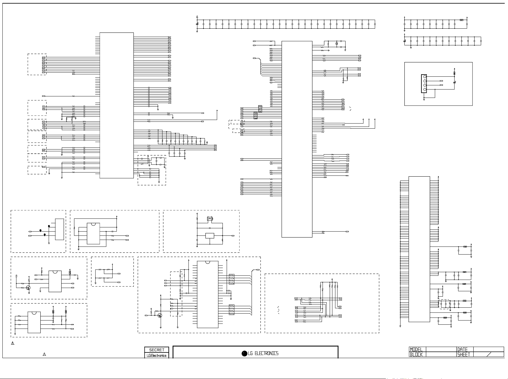
A CB
Copyright © 2009 LG Electronics. Inc. All right reserved.
Only for training and service purposes
LGE Internal Use Only
1
2
3
4
HDMI
002:F1;012:C3
COMPONENT1
DSUB
COMPONENT2
CVBS
S-VIDEO
TV/MNT
5
ISP Port
001:H1;009:F4
001:H1;009:F4
6
Serial FLASH MEMORY for BOOT
009:I3
SPI_CS
D3.3V_2
009:I2
SPI_DO
009:I2
7
8
Flash_WP_1
EEPROM
0
R2127
0
R2125
0
R2126
R101
OPT
R102
Q100
KRC103S
10K
R103
0
C
B
0
E
IC104
AT24C512BW-SH-T
A0
1
A1
2
A2
2mA
3
0xA0
GND
4
AV2_CVBS_IN
AV1_CVBS_IN
ISP_RXD
ISP_TXD
$0.418
HDMI_CLK+
HDMI_CLKHDMI_RX0+
HDMI_RX0HDMI_RX1+
HDMI_RX1HDMI_RX2+
HDMI_RX2HDMI_SDA
HDMI_SCL
DSUB_HSYNC
DSUB_VSYNC
COMP1_PR
COMP1_Y
COMP1_PB
DSUB_R
DSUB_G
DSUB_B
COMP2_PR
COMP2_Y
COMP2_PB
AV1_Y_IN
AV1_C_IN
FE_VMAIN
ISP Debug port for S5
D3.3V_2
R105
4.7K
R104
33
VCC
8
WP
7
SCL
6
SDA
5
002:F3
002:F3
002:F3
002:F3
002:F3
002:F3
002:F3
002:F3
002:F3
002:F3
HDMI_CEC_RX
001:B2
001:B1
001:B1
001:F2
001:F2
001:F3
001:F2
001:F2
001:B2
001:B1
001:B1
001:B2;001:C3
001:B2;001:C3
001:B2
001:B2
005:C3
IC101
MX25L3205DM2I-12G
CS#
1
$0.76
SO
2
25mA
WP#
3
GND
4
D3.3V_2
L104
C100
0.1uF
R2111 33
R2112 33
SMW250-04
1
2
3
4
F
GD
HE
D1.26V_VDDC
C188
C193
0.1uF
0.1uF
S6_Reset_IN
S6_Reset
009:D7
009:E8
009:D7
009:E8
009:E8
009:D8
009:D7
009:B8;009:C6;009:H8
009:B8;009:C6;009:H8
009:H7
009:H8
001:H1;009:A6
001:H1;009:A6
009:C7
009:C7
017:C6;017:H6
016:C3
014:G4;012:C3;009:I3
017:A3
017:H6
016:C3;017:A3
014:G4;009:I3
014:G4
001:B3
PCM_A[0-7]
AR102
C198
0.1uF
C2115
C2104
0.1uF
0.1uF
0.1uF
470
R230
012:F2
0
R187
OPT
009:F6
R2177 33
OPT
R2178 33
OPT
R2179 33
OPT
R2180 33
OPT
R2181 33
OPT
R2182 33
OPT
R2183 33
OPT
R2184 33
OPT
PCM_A[0]
PCM_A[1]
PCM_A[2]
PCM_A[3]
PCM_A[4]
PCM_A[5]
PCM_A[6]
PCM_A[7]
OPT
R2172 33
OPT
R2123 33
OPT
R2124 33
OPT
R178 33
OPT
R205 33
OPT
R206 33
OPT
R207 33
OPT
R208 33
OPT
R209 33
OPT
R210 33
OPT
R211 33
OPT
R212 33
OPT
R213 33
AR103
OPT
R214 33
22
22
0
R215
0
R216
0
R217
0
R218
22
R191
22
R192
R183 22
R184 22
R194
0
R195 100
R2190 0
R2191
0
R193 0
R112 0
OPT
100
R196
100
R200
100
R248
R221 100
100
R201
R219 100
R255 100
100
R179
22
OPT
R2160
C183
C178
C172
C169
1
KIA7427F
C175
0.1uF
0.1uF
0.1uF
0.1uF
0.1uF
CH1
CH2
AUDIO_MASTER_CLK
MS_LRCK
MS_SCK
MS_LRCH
R247
10K
EEPROM_SCL
EEPROM_SDA
HDMI_TX_SEL
HDMI_RES_SEL
WIHD_TX_INT
HDMI_TX_INT
HDMI_TX_DDC_SEL
HDMI_TX_RESETb
HDMI_RX_INT
HDMI_RX_RESETb
AV1_SVIDEO_DET
S6_Reset
/PF_CE0
/PF_CE1
ISP_RXD
ISP_TXD
DBG_RX
DBG_TX
/PF_OE
/PF_WE
PF_ALE
PF_WP
/F_RB
SDA0
SCL0
PWM0
PWM1
5V_HDMI_4
017:A2
017:A2
017:A2
017:A2
12
SW100
4 3
TMSV1 53BRA
C213
6.3V
4.7uF
IC103
OUT
3
2
GND
C166
C163
0.1uF
330uF
IC100
LGE3369A (Saturn6 Non RM)
@compC
F1
RXACKP
F2
RXACKN
G2
RXA0P
G3
RXA0N
H3
RXA1P
G1
RXA1N
H1
RXA2P
H2
RXA2N
A1
DDCD_A_DA
B2
DDCD_A_CK
A2
HOTPLUG_A
C3
RXBCKP
B1
RXBCKN
C1
RXB0P
C2
RXB0N
D2
RXB1P
D3
RXB1N
E3
RXB2P
D1
0.047uF
0.047uF
1000pF
0.047uF
0.047uF
0.047uF
0.047uF
0.047uF
1000pF
0.047uF
0.047uF
0.047uF
1000pF
0.047uF
0.047uF
0.047uF
CAT24WC08W-T
A0
1
A1
2
A2
3
VSS
4
IC105
$0.199
0xA8
1mA
RXB2N
E1
DDCD_B_DA
F3
DDCD_B_CK
E2
HOTPLUG_B
AE8
RXCCKP
AD8
RXCCKN
AD9
RXC0P
AF8
RXC0N
AF9
RXC1P
AE9
RXC1N
AE10
RXC2P
AD10
RXC2N
AE7
DDCD_C_DA
AF7
DDCD_C_CK
AD7
HOTPLUG_C
J3
CEC
N2
HSYNC0/SC1_ID
N1
VSYNC0/SC1_FB
P2
RIN0P/SC1_R
R3
GIN0P/SC1_G
R1
BIN0P/SC1_B
P3
SOGIN0/SC1_CVBS
P1
RINM
T3
BINM
R2
GINM
K3
HSYNC1/DSUB_HSYNC
K2
VSYNC1/DSUB_VSYNC
L1
RIN1P/DSUB_R
L3
GIN1P/DSUB_G
K1
BIN1P/DSUB_B
L2
SOGIN1
V1
RIN2P/COMP_PR+
V2
GIN2P/COMP_Y+
U1
BIN2P/COMP_PB+
V3
SOGIN2
J5
VSYNC2
U3
CVBS1/SC1_CVBS
U2
CVBS2/SC2_CVBS
T1
CVBS3/SIDE_CVBS
T2
VCOM1
M1
CVBS4/S-VIDEO_Y
M2
CVBS6/S-VIDEO_C
N3
CVBS5
M3
CVBS7
W1
CVBS0/RF_CVBS
Y3
VCOM0
Y2
CVBSOUT0/SC2_MNTOUT
AA2
CVBSOUT1
VCC
8
WP
7
SCL
6
SDA
5
R181
R182 22
D5.0V_1
C197
0.1uF
22
R142
0
R143
0
R144 100
OPT
R145 100
C101 0.047uF
47
R120
C102
R121 47
47
C103
R122
470
R123
C104
C105 0.047uF
47
R124
C106
R125 47
47
C107
R126
R109
R107
10K
10K
R146 22
R149 22
R127
47
C113
C108
R128
47
R129 47
C114
470
C109
R130
R133
C115
47
R134 47
C116
R135
C117
47
470
C110
R136
C111 0.047uF
R113 47
R114 47
C112
C118 0.047uF
R137 47
R138 47
C119 0.047uF
C120
R115
47
C121
R116 47
R140 47
C124 0.047uF
R141 47
C125 0.047uF
R139
100
C122 0.047uF
100
C123 0.047uF
R117
100
R2122
HDCP EEPROM
P101
R106
4.7K
EEPROM_SCL
EEPROM_SDA
SPDIF_IN
SPDIF_OUT
AUOUTR0/HP_ROUT
AUOUTL0/HP_LOUT
AUOUTR1/SC1_ROUT
AUOUTL1/SC1_LOUT
AUOUTR2/SC2_ROUT
AUOUTL2/SC2_LOUT
I2S_OUT_MCK
I2S_OUT_WS
I2S_OUT_BCK
I2S_OUT_SD
I2S_IN_SD
AE16
LVA0P
AD16
LVA0M
AD15
LVA1P
AF16
LVA1M
AF15
LVA2P
AE15
LVA2M
AD13
LVA3P
AF14
LVA3M
AF13
LVA4P
AE13
LVA4M
AE14
LVACKP
AD14
LVACKM
AE20
LVB0P
AD20
LVB0M
AD19
LVB1P
AF20
LVB1M
AF19
LVB2P
AE19
LVB2M
AD17
LVB3P
AF18
LVB3M
AF17
LVB4P
AE17
LVB4M
AE18
LVBCKP
AD18
LVBCKM
AA3
AUR0
Y1
AUL0
AE1
AUR1
AF3
AUL1
AE3
AUR2
AE2
AUL2
AA1
AUR3
AB1
AUL3
AB2
AUR4
AC2
AUL4
AB3
AUR5
AC3
AUL5
W3
SIF0P
W2
SIF0M
F11
E9
AF1
AF2
AD3
AD1
AC1
AD2
A8
B7
C7
D8
C8
K4
C127
VCLAMP
H4
REFP
J4
REFM
G4
R152 390
REXT
AE5
AUCOM
AE4
AUVRM
AF4
AUVRP
AD4
AUVAG
009:B8;009:F3;009:H8
009:B8;009:F3;009:H8
C134 2.2uF
C135
2.2uF
C136
2.2uF
C137
2.2uF
C138 2.2uF
C139
2.2uF
C140 2.2uF
C141
2.2uF
C142
2.2uF
C143 2.2uF
C144 2.2uF
C145 2.2uF
C146 0.1uF
C147 0.1uF
OPT
R269 22
R159 100
100
OPT
R164
100
OPT
R165
100
OPT
R166
100
OPT
R167
100
OPT
R168
100
OPT
R169
R160 22
R161 22
R162 22
R163 22
D3.3V_1
0.1uF
C148
0.1uF
1%
C128 0.1uF
10V
C129 10uF
C130 0.1uF
C132
1uF
C133 4.7uF
Close to IC
as close as possible
016:C2
LVA_0P
016:C2
LVA_0M
016:C2
LVA_1P
016:C2
LVA_1M
016:C2
LVA_2P
016:C2
LVA_2M
016:C2
LVA_3P
016:C2
LVA_3M
016:C3
LVA_4P
016:C2
LVA_4M
016:C2
LVA_CKP
016:C2
LVA_CKM
016:C1
LVB_0P
016:C1
LVB_0M
016:C2
LVB_1P
016:C1
LVB_1M
016:C2
LVB_2P
016:C2
LVB_2M
016:C2
LVB_3P
016:C2
LVB_3M
016:C2
LVB_4P
016:C2
LVB_4M
016:C2
LVB_CKP
016:C2
LVB_CKM
001:E2
AV2_R_IN
001:E1
AV2_L_IN
001:E2
COMP1_R_IN
001:E2
COMP1_L_IN
001:E1
AV1_R_IN
001:E1
AV1_L_IN
001:E3
COMP2_R_IN
001:E3
COMP2_L_IN
001:H4
PC_R_IN
001:H4
PC_L_IN
R171
47
R172 47
OPT
OPT
OPT
R173
22K
R170
22K
C153
0.01uF
R174
C151
0.01uF
OPT
C150
0.1uF
C149
0.1uF
22K
C156
0.01uF
OPT
OPT
C154
C152
22pF
22pF
OPT
OPT
S6 Reset
4V
005:C2
FE_SIF
001:F5;017:A2
SPDIF_OUT
OPT
OPT
OPT
R176
22K
R175
22K
C158
0.01uF
C160
0.01uF
R177
22K
C159
0.01uF
OPT
OPT
OPT
C157
C155
22pF
22pF
OPT
OPT
D3.3V_1
R228
470
VCC
C212
0.022uF
16V
C2109
C2120
C2119
C2137
0.1uF
0.1uF
0.1uF
IC100
LGE3369A (Saturn6 Non RM)
@compC
D4
HWRESET
AC16
PCMD0/CI_D0
AA15
PCMD1/CI_D1
AA16
PCMD2/CI_D2
AC6
PCMD3/CI_D3
Y10
PCMD4/CI_D4
Y11
PCMD5/CI_D5
Y12
PCMD6/CI_D6
Y13
PCMD7/CI_D7
AB16
PCM_A0/CI_A0
AC15
PCM_A1/CI_A1
AC14
PCM_A2/CI_A2
AB14
PCM_A3/CI_A3
AC12
PCM_A4/CI_A4
AB8
PCM_A5/CI_A5
AC13
PCM_A6/CI_A6
AA9
PCM_A7/CI_A7
AB5
PCM_A8/CI_A8
AA4
PCM_A9/CI_A9
V4
PCM_A10/CI_A10
Y4
PCM_A11/CI_A11
AB9
PCM_A12/CI_A12
AA7
PCM_A13/CI_A13
AD6
PCM_A14/CI_A14
AA14
PCM_RST/CI_RST
AB18
PCM_CD/CI_CD
Y5
/PCM_OE
AB15
PCM_REG/CI_CLK
AA10
PCM_WAIT/CI_WACK
AC8
GPIO_PM5/INT1/GPIO139
/PCM_IRQA
AC7
GPIO_PM6/INT2/GPIO140
/PCM_WE
AA5
GPIO131/LDE/SPI_WPn1
PCM_IOWR/CI_WR
W4
PCM_IOR/CI_RD
T4
GPIO132/LHSYNC/SPI_WPn
/PCM_CE
AE6
GPIO60/PCM2_RESET/RX1
/PF_CE0
AF6
GPIO62/PCM2_CD_N/TX1
/PF_CE1
AA12
/PF_OE
AA11
/PF_WE
AC9
PF_ALE
Y14
PF_AD15
AB11
LHSYNC2/I2S_OUT_MUTE/RX1
F_RBZ
F8
D11
AB21
AC21
J1
J2
W5
V5
AB13
AB12
AD12
AA13
A4
B4
F4
E4
C4
AC11
D9
D10
D7
E11
E8
E10
D6
D5
C5
UART2_TX/SCKM
UART2_RX/SDAM
DDCR_DA
DDCR_CK
DDCA_CLK
DDCA_DA
UART_RX2
UART_TX2
PWM0
PWM1
PWM2
PWM3
SAR0
SAR1
SAR2
SAR3
IRIN
GPIO44
GPIO96
GPIO88
GPIO90/I2S_OUT_MUTE
GPIO91
GPIO97
GPIO98
GPIO99
GPIO103/I2S_OUT_SD3
GPIO102
GPIO79/LVSYNC2/TX1
GPIO43/PCM2_IRQA_N
C2124
C2123
0.1uF
0.1uF
TESTPIN/GND
/SPI_CS
USB_DP_1
USB_DM_1
USB_DM_2
USB_DP_2
GPIO_PM0/GPIO134
GPIO_PM1/GPIO135
GPIO_PM2/GPIO136
GPIO_PM3/GPIO137
GPIO_PM4/GPIO138
GPIO130/LCK
LVSYNC/GPIO133
UART2_RX/GPIO84
UART2_TX/GPIO85
UART1_RX/GPIO86
UART1_TX/GPIO87
GPIO42/PCM2_CE_N
TS0_SYNC
TS0_VLD
TS0_CLK
TS1_SYNC
TS1_VLD
TS1_CLK
ET_TXD0
ET_TXD1
ET_TX_CLK
ET_RXD0
ET_RXD1
ET_TX_EN
ET_MDIO
C2126
C2125
0.1uF
0.1uF
B3
XIN
A3
R231 0
XOUT
E6
R232 0
AE11
R225 33
SPI_DI
AF12
SPI_DO
AE12
R226 33
AD11
R227 33
SPI_CK
B5
R222 0
R223 0
A5
AC10
R234 0
AB10
R233 0
E5
R237
F5
R119 100
G5
R244 100
H5
R245 100
F6
R241 100
R272
G6
H6
R246
AC17
R2193 100
AB17
R220 100
AF11
R238
AA18
R239 0
AA17
R240 0
E7
R202
AC18
R2185
C6
R203 0
F9
R2186
F10
A6
R267
B6
R268 22
AF5
R2194 22
AF10
R2187
AA8
TS0_D0
Y8
TS0_D1
Y9
TS0_D2
AB7
TS0_D3
AA6
TS0_D4
AB6
TS0_D5
U4
TS0_D6
AC5
TS0_D7
AC4
AD5
AB4
AB19
TS1_D0
AA20
AC19
AA19
C10
B11
R235 100
A9
R243
C11
R110 100
C9
R2188 100
B10
R249 100
A10
R250 100
ET_MDC
B9
R2189 100
A11
R111 100
ET_COL
A7
R224 100
GPIO67
B8
R242
GPIO68
OPT
100
100
100
100
22
22
R251 100
100
C2127
0.1uF
0
OPT
OPT
OPT
22
OPT
OPT
OPT
OPT
OPT
22
R99 33
R98 33
R97 33
R96 33
100
R252
1M
OPT
C2129
C2128
0.1uF
0.1uF
X100
12MHz
014:G4;012:C3;009:F5
014:G4;009:F5
014:G4;009:F5
009:A7
009:H8
009:H8
014:H3
001:B3;001:C1
001:B3;001:C2
001:B2;001:C2
001:B2;001:C3
C186
20pF
C187
20pF
15K
R254
001:H3
001:H1
005:H1
Addr:10101--
IC102
HY27US08121B-TPCB
MCU BOOT STRAP
D3.3V_1
OPT
R150 1K
R151 1K
10 : BOOT 51
11 : BOOT RISC
PWM0
009:F4
PWM1
009:F4
D3.3V_2
L110
VCC
8
HOLD#
7
0.1uF
C126
SCLK
6
SPI_CK
009:I2
009:I2
SI
SPI_DI
5
D5.0V_1
OPT
L105
4.7K
4.7K
OPT
OPT
R118
R132
EEPROM_SCL
009:C6;009:F3;009:H8
EEPROM_SDA
009:C6;009:F3;009:H8
R147 1K
R148
OPT
1K
NAND FLASH MEMORY
/PF_CE0
H : Serial Flash
L : NAND Flash
/PF_CE1
H : 16 bit
L : 8 bit
/F_RB
009:F3
/PF_OE
009:F3
/PF_CE0
009:F3
D3.3V_2
R153
D3.3V_2
R180
R258
0
OPT
10K
PF_WP
009:F3
10K
Q101
KRC103S
OPT
/PF_CE1
PF_ALE
/PF_WE
OPT
R154
1K
009:F3
009:F3
009:F3
D3.3V_2
NC_1
1
NC_2
2
1386 WON
NC_3
3
NC_4
1K
R156
R157 1K
R155
1K
4
NC_5
30mA
5
NC_6
6
R/B
R158 3.9K
7
RE
8
CE
9
NC_7
10
NC_8
11
OPT
VCC_1
0.1uF
C131
12
VSS_1
13
NC_9
14
NC_10
15
CLE
16
ALE
17
WE
18
WP
19
NC_11
20
NC_12
21
NC_13
22
NC_14
23
NC_15
24
D3.3V_2
NC_28
48
NC_27
47
NC_26
46
NC_25
45
AR100
I/O7
44
I/O6
43
I/O5
42
I/O4
41
NC_24
40
NC_23
C161
39
10uF6.3V
PRE
38
VCC_2
37
C162 0.1uF
VSS_2
36
NC_22
35
NC_21
34
NC_20
33
AR101
I/O3
32
I/O2
31
I/O1
30
I/O0
29
NC_19
28
NC_18
27
NC_17
26
NC_16
25
PCM_A[0-7]
PCM_A[7]
PCM_A[6]
PCM_A[5]
PCM_A[4]
22
PCM_A[3]
PCM_A[2]
PCM_A[1]
PCM_A[0]
22
CH2
CH2
014:G5;017:F4;017:H5
014:G4;017:F5;017:F4
CH4
HDMI SW
CH4
HDMI_TX
I2C
CH2
R2117 0
R2118 0
R2102 0
R2103 0
R2104 0
R2105 0
R2115 0
R2116 0
R2100 0
R2101 0
R2113 0
R2114 0
OPT
OPT
FE_DEMOD_SDA
005:H2
FE_DEMOD_SCL
005:H2
SDA_HDMI
017:E3
SCL_HDMI
017:E3
TDA9996_SDA
002:G6
TDA9996_SCL
002:G6
SDA_WIHD
SCL_WIHD
SDA_MCU
012:C3
SCL_MCU
012:C3
D3.3V_1
R2107
4.7K
4.7K
R2108
4.7K
R2604.7K
R266
R2109 1.2K
R2110 1.2K
OPT
OPT
SDA0
SCL0
EEPROM_SDA
EEPROM_SCL
SDA1
SCL1
I J K L
D3.3V_VDDP
F7
L9
M9
N4
N9
P4
P9
R4
R9
T5
T9
U5
GND_2
GND_3
GND_4
GND_5
GND_6
GND_7
GND_8
GND_9
GND_10
GND_11
GND_12
GND_13
GND_14
GND_15
GND_16
GND_17
GND_18
GND_19
GND_20
GND_21
GND_22
GND_23
GND_24
GND_25
GND_26
GND_27
GND_28
GND_29
GND_30
GND_31
GND_32
GND_33
GND_34
GND_35
GND_36
GND_37
GND_38
GND_39
GND_40
GND_41
GND_42
GND_43
GND_44
GND_45
GND_46
GND_47
GND_48
GND_49
GND_50
GND_51
GND_52
GND_53
GND_54
GND_55
GND_56
GND_57
GND_58
GND_59
GND_60
GND_61
GND_62
GND_63
GND_64
GND_65
GND_66
GND_67
GND_68
GND_69
GND_70
GND_71
GND_72
GND_73
C167
0.1uF
C168
0.1uF
UB01123-4HHS-4F
IC100
@compC
C170
0.1uF
C171
0.1uF
P1101
AVDD_DDR_1
AVDD_DDR_2
AVDD_DDR_3
AVDD_DDR_4
AVDD_DDR_5
AVDD_DDR_6
AVDD_DDR_7
AVDD_DDR_8
AVDD_DDR_9
AVDD_DDR_10
AVDD_DDR_11
AVDD_MEMPLL_1
AVDD_MEMPLL_2
AVDD_MEMPLL_3
USB D OWN S TREAM
5
VDDC_10
VDDC_11
VDDC_12
VDDC_13
VDDC_14
VDDC_15
VDDC_16
VDDC_17
VDDC_18
VDDC_19
VDDC_20
VDDC_21
VDDC_22
VDDC_23
VDDC_24
VDDC_25
VDDC_26
VDDC_27
AVDD_AU
AVDD_LPLL
AVDD_MPLL
AVDD_33_1
AVDD_33_2
AVDD_33_3
AVDD_33_4
AVDD_33_5
AVDD_DM
AVDD_USB
C173
0.1uF
C174
0.1uF
VDDC_1
VDDC_2
VDDC_3
VDDC_4
VDDC_5
VDDC_6
VDDC_7
VDDC_8
VDDC_9
VDDP_1
VDDP_2
VDDP_3
VDDP_4
VDDP_5
VDDP_6
VDDP_7
VDDP_8
1234
C176
0.1uF
C177
0.1uF
D1.26V_VDDC
D16
D17
D18
D19
D20
H18
H19
H20
J20
K20
L20
M20
P7
R7
T7
T22
U7
U20
U22
V7
V22
W11
W12
W19
W20
W22
Y22
H9
H10
H11
H12
N20
P20
W9
W10
W7
D1.8V_DDR
G12
G13
H13
H14
H15
H16
W14
W15
W16
W17
W18
H17
T20
V20
R20
H7
C191
0.1uF
J7
K7
L7
M7
N7
W8
H8
AVDD_OTG : 22.96mA
C179
0.1uF
C180
0.1uF
USB_DM_DBG
009:I2
USB_DP_DBG
009:I2
D3.3V_VDDP
D3.3V_AVDD_MPLL
C201
10uF
10V
AVDD_MPLL : 7.76mA
C204
0.1uF
BLM18PG121SN1D
C192
0.1uF
C184
0.1uF
C185
0.1uF
CB3216PA501E
VDDC : 970mA
C200
0.1uF
C205
0.1uF
L102
D5.0V_1
D3.3V_1
L1100
C2130
C2131
0.1uF
0.1uF
009:B7
009:A7
009:A7
009:B7
OPT
15K
R256
OPT
WIHD_TX_INT
HDMI_RX_INT
RF_SWITCH_SEL
FE_BOOSTER_CTL 009:BC15
Flash_WP_1
SDA1
CH4
SCL1
USB_OCD
FE_TS_SERIAL 009:U20
FE_TS_SYN 009:U21
FE_TS_VAL_ERR 009:U20
FE_TS_DATA_CLK 009:U21
AV1_CVBS_DET
AV2_CVBS_DET
COMP2_DET
COMP1_DET
DSUB_DET
VGA_EEPROM_WP
/FE_RESET
USB_CTL
009:F3
CH2
009:F3
HW IIC
009:B8;009:C6;009:F3
009:B8;009:C6;009:F3
CH1
009:I3
009:I3
CH4
C2134
C2132
C2133
C2135
0.1uF
0.1uF
0.1uF
10uF
SPI_DI
SPI_DO
SPI_CS
SPI_CK
ANOTHER USB PORT USE FOR DEBUGGING OK????
USB_DP
USB_DM
009:K2
USB_DM_DBG
USB_DP_DBG
009:K2
5V_HDMI_15V_HDMI_3
5V_HDMI_2
LGE3369A (Saturn6 Non RM)
014:H3
C164
0.1uF
D1.8V_DDR
C165
330uF
4V
E16
E17
E18
L10
L11
L12
L13
L14
L15
L16
L17
L18
M10
M11
M12
M13
M14
M15
M16
M17
M18
N10
N11
N12
N13
N14
N15
N16
N17
N18
P10
P11
P12
P13
P14
P15
P16
P17
P18
R10
R11
R12
R13
R14
R15
R16
R17
R18
T10
T11
T12
T13
T14
T15
T16
T17
T18
W13
Y21
AA23
BLM18PG121SN1D
C189
C195
0.1uF
0.1uF
C194
C190
0.1uF
0.1uF
C1101
10uF
16V
For Debuggging
VDDP : 102.3mA
BLM18PG121SN1D
C215
0.1uF
BLM18PG121SN1D
C206
C209
0.1uF
0.1uF
BLM18PG121SN1D
C211
0.1uF
BLM18PG121SN1D
C203
C207
C202
0.1uF
0.1uF
0.1uF
C210
0.1uF
C208
0.1uF
D3.3V_1
L101
C196
0.1uF
C2105
C199
C2110
0.1uF
0.1uF
0.1uF
AVDD_AU : 36.11mA
D3.3V_1
L109
C219
0.1uF
AVDD_MEMPLL : 23.77mA
D3.3V_1
L106
C216
0.1uF
D3.3V_1
L108
AVDD_LPLL : 4.69mA
C218
0.1uF
D3.3V_1
AVDD_33 : 281mA
L103
C214
0.1uF
D3.3V_1
AVDD_DM : 0.03mA
L107
BLM18PG121SN1D
C217
0.1uF
C2136
10uF
THE SYMBOL MARK OF THIS SCHEMETIC DIAGRAM INCORPORATES
SPECIAL FEATURES IMPORTANT FOR PROTECTION FROM X-RADIATION.
FILRE AND ELECTRICAL SHOCK HAZARDS, WHEN SERVICING IF IS
ESSENTIAL THAT ONLY MANUFATURES SPECFIED PARTS BE USED FOR
THE CRITICAL COMPONENTS IN THE SYMBOL MARK OF THE SCHEMETIC.
JUNO-BOX
MSD3369GV
09
17
Page 32
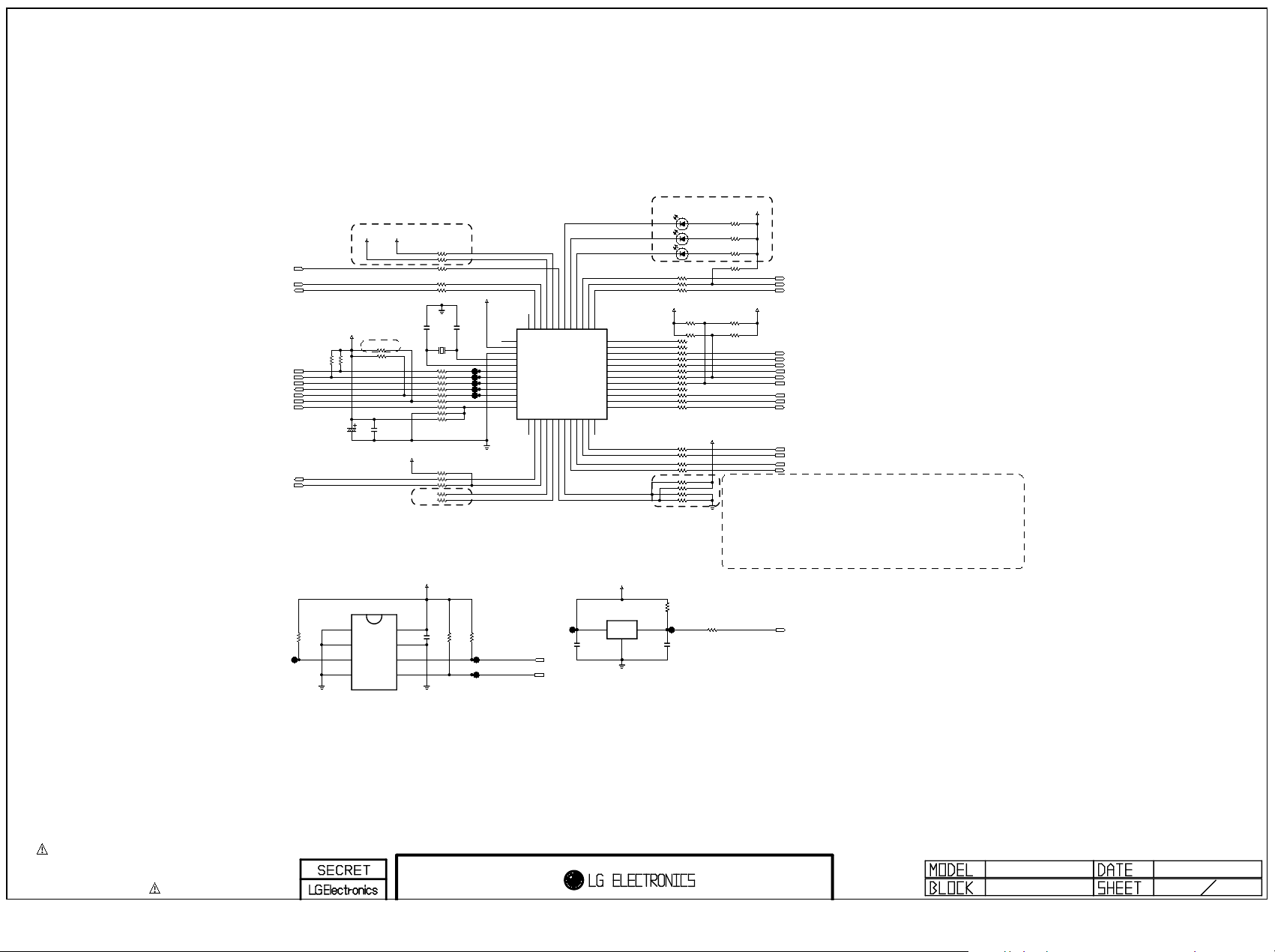
A CB
Copyright © 2009 LG Electronics. Inc. All right reserved.
Only for training and service purposes
LGE Internal Use Only
F
GD
HE
1
2
3
4
MICRO-CONTROLLER
017:F4
012:F5
014:F6
009:G8
009:G8
012:D5
012:D5
014:G6
002:F1;009:B3
014:G4;009:F5;009:I3
014:E2
014:E2
WIHD_PWR_MNT
MICOM_RESETb
UART_SELECT
R455
4.7K
SDA_MCU
SCL_MCU
MICOM_SDA_M
MICOM_SCL_M
IR_IN
HDMI_CEC_RX
WIHD_TX_INT
FRONT_INT
D3.3V_L
R456
4.7K
D3.3V_1
HDMI regulation
R401 27K
R402 4.7K
C401
C400
0.1uF
47uF
16V
16V
POWER
D5.0V_1
MONITORING
P5.0V_ST
WIHD I2C (BACK-UP)
R404 4.7K
R405 100
R406 0
R407 100
C403
20pF
50V
R408 22
R409 22
R410 22
R411 22
R412 22
R413 100
R414 100
R415 OPT
R416 4.7K
R417 4.7K
R418 100FRONT_RESETb
R419 100
R420 OPT
R421 OPT
D3.3V_L
C404
20pF
50V
X400
24MHz
VDD33V
GPIOB6/SSDA
TP403
GPIOB5/SSCL
TP404 R434 100
GPIOB4/P05
TP405
GPIOB3/P04
TP406
GPIOB2/IR
TP407
GPIOB1/IRQ3/CEC
GPIOB0/IRQ2
NC1
GND
OSCO
OSCI
GPIOE1/PWM1
NRST47GPIOE0/PWM0
NC5
45
46
48
1
2
3
4
5
WT61P8-RG480WT
6
7
8
9
10
11
12
13
14
15
16
NC2
GPIOC7/P17/IRQ1
GPIOC6/P16/IRQ0
GPIOC5/P15/TXD0
GPIOE6/VIN2
GPIOE5/P07
GPIOE4/LPWM/P06
GPIOE3/PWM3
GPIOE2/PWM2
40
41
42
43
44
IC401
NEW
20mA
17
18
GPIOC3/AD319GPIOC2/AD220GPIOC1/AD121GPIOC0/AD0
GPIOC4/P14/RXD0
GPIOD1/HIN2
GPIOD0/HIN1
GPIOE7/VIN1
37
38
39
22
24
NC3
DSDA123DSCL1
GPIOD2/P10/AD4
36
GPIOD3/P11/AD5
35
GPIOD4/P12/AD6
34
GPIOD5/P13/AD7
33
GPIOD6/TXD1
32
GPIOD7/RXD1
31
GPIOA0/PWM4/P00
30
GPIOA1/PWM5/P01
29
GPIOA2/PWM6/P02
28
GPIOA3/PWM7/P03
27
GPIOA4/DSCL2
26
GPIOA5/DSDA2
25
WIRELESS STATUS
INDICATOR
PV
D400 SML-201MT
PV
D401 SML-201MT
PV
D402 SML-201MT
R425 1K
R426 100
R427 100
D3.3V_L
R457
4.7K
R458
4.7K
R428 0
R429 0
R430 0
R431 22
R432 220
R433 220
R435 100
R436 OPT
R437 OPT
R438 100
R439 100
P5.0V_ST
R440 22
R441 22
R442 100
R443 100
R444 3.3K
R445 3.3K
R446 6.8K
R447 6.8K
N7N)N$N)
D3.3V_L
R449 1K
R450 1K
R451 1KR403 4.7K
R452 4.7K
S6_Reset_IN
WIHD_TX_RESETb
WIHD_PWR_EN
P5.0V_ST
R453
OPT
4.7K
R454
OPT
4.7K
D3.3V_EN
PWR_CTRL
MICOM_UART_TXD
MICOM_UART_RXD
MICOM_SCL_S
MICOM_SDA_S
HDMI_CEC_TX
FAN_W_DETECT
FAN_W_ONOFF
RGB_DDC_SCL
RGB_DDC_SDA
FAN_S_DETECT
FAN_S_ONOFF
MODEL CONFIGURATION
PRODUCT OPTION ---> ADC2
MARKET OPTION ---> ADC 3
009:G1
014:G4
004:F5
004:G3
004:C2
014:F6
014:C5
014:E2
014:E2
017:F2;017:F4
014:C4
014:C4
001:H1
001:H1
014:E4
014:E4
0V Jupiter (NOT USED)
3V Juno
0V EU OPTION ( KEY INPUT SCART)
3V US OPTION ( TV, COMP1/2, AV1(SVIDEO), AV2, HDMI1/2/3/4, RGB, POWER ON/OFF
CHINA FOLOW US OPTION / SVIDEO HAS PRIOTY THAN AV1
EEPROM MICOM RESET
M24C16-WMN6T
1
1
2
2
3
3
4
4
TP400
R400
47K
5
6
THE SYMBOL MARK OF THIS SCHEMETIC DIAGRAM INCORPORATES
SPECIAL FEATURES IMPORTANT FOR PROTECTION FROM X-RADIATION.
FILRE AND ELECTRICAL SHOCK HAZARDS, WHEN SERVICING IF IS
ESSENTIAL THAT ONLY MANUFATURES SPECFIED PARTS BE USED FOR
THE CRITICAL COMPONENTS IN THE SYMBOL MARK OF THE SCHEMETIC.
IC400
D3.3V_L
8
8
C402
R422
R423
0.1uF
4.7K
7
7
6
6
5
5
4.7K
16V
MICOM_SCL_M
TP401
TP402
MICOM_SDA_M
TP408
012:C3
012:C3
C405
0.1uF
16V
I
D3.3V_L
IC402
KIA7029AF
20mA
2
R424
47K
R448 0
MICOM_RESETb
012:C2
TP409
3O1
G
C406
0.1uF
16V
JUNO-BOX
MICOM
12
17
Page 33
A
Copyright © 2009 LG Electronics. Inc. All right reserved.
Only for training and service purposes
LGE Internal Use Only
B C
D E
F
G
H
USB PORT (FRONT)
1
SMD Gasket Option
GAS1
GAS1
MDS61887701
GAS2
MDS61887701
GAS2
2
1. Bottom of P1105
2. Between under of JK801 and IC1001
1
2
FRONT I/F
P1103
12507WS-08L
NEW
1
2
3
4
5
6
7
8
9
TP1106
C1122
10uF
C1117
0.1uF
16V
L1105
BLM18SG121TN1D
16V
C11241000pFOPT
D1103ADUC30S03010L_AMODIODE
D1104ADUC30S03010L_AMODIODE
C11181000pFOPT
D1105ADUC30S03010L_AMODIODE
C11191000pFOPT
C11251000pFOPT
D1106ADUC30S03010L_AMODIODE
Close to P1103.
P5.0V_ST
L1106BLM18PG121SN1D
FRONT_RESETb
MICOM_SDA_S
R11230
MICOM_SCL_S
R11240
L1107BLM18PG121SN1D
FRONT_INT
012:C4
012:F3
012:F3
012:C4
P1100
KJA-UB-4-0004
1234
USB DOW N ST REA M
5
Rset=CLF(v)/Iout(A)
Iout=2A, CLF=250V
Iout=1A, CLF=243V
+5V_USB_1
014:H1
180
R1104
D1107
ADMC5M03200L
5.6V
OPT
IC1101
MIC2009YM6-TR
VOUT
6
0.3mA
ILIMIT
5
FAULT/
4
1.5A limitation settting
R1105
47
D1108
ADMC5M03200L
5.6V
OPT
D3.3V_2
R1106
4.7K
VIN
1
GND
2
ENABLE
3
OPT
R1109
10K
C1109
10uF
10V
009:I2
009:I2
USB_DM
USB_DP
D5.0V_1
USB_CTL
USB_OCD
+5V_USB_1
L1102
CB3216PA501E
C1110
0.1uF
014:G2
C1104
330uF
25V
3
FAN I/F For WIRELESS
R1121
4.7K
R1122
330
R1125 0
C
Q1100
2SC3052
E
P5.0V_ST
S
Q1101
G
RTR030P02
D
CIC21J601
L1108
600 L1109
C1116
C1120
0.1uF
10uF
16V
16V
P1104
SMW200-03
1
2
3
012:F4
012:F4
P5.0V_ST
4
012:F3
012:F3
FAN_W_DETECT
FAN_W_ONOFF
B
FAN I/F For SYSTEM
FAN_S_DETECT
FAN_S_ONOFF
P5.0V_ST
B
R1128
4.7K
R1129
330
R1130 0
C
Q1102
2SC3052
E
P5.0V_ST
G
L1110
600
CIC21J601
S
Q1103
RTR030P02
D
C1126
0.1uF
16V
CIC21J601
P6.0V
CIC21J601
600
L1111
600
OPT
C1127
10uF
16V
P1105
SMW200-03
1
2
3
009:F5
012:F2
009:F5;009:I3
012:C3;009:F5;009:I3
017:F5;017:F4;009:G8
017:F4;017:H5;009:G8
HDMI_RX_RESETb
WIHD_TX_RESETb
HDMI_RX_INT
WIHD_TX_INT
SCL_WIHD
SDA_WIHD
R1126 0
R1127 0
WiHD TX I/F
TP1105
C1121
0.1uF
16V
D5.0V_W
C1123
10uF
16V
P1102
12507WS-12L
1
2
3
4
5
6
7
8
9
10
11
12
13
5
6
THE SYMBOL MARK OF THIS SCHEMETIC DIAGRAM INCORPORATES
SPECIAL FEATURES IMPORTANT FOR PROTECTION FROM X-RADIATION.
FILRE AND ELECTRICAL SHOCK HAZARDS, WHEN SERVICING IF IS
ESSENTIAL THAT ONLY MANUFATURES SPECFIED PARTS BE USED FOR
THE CRITICAL COMPONENTS IN THE SYMBOL MARK OF THE SCHEMETIC.
RS-232 Switching
001:C4;014:F5
009:F4
012:F3
SYS_UART_RXD
DBG_RX
MICOM_UART_RXD
R1107 0 OPT
R1108 0
TP1100
TP1101
IC1102
MC14053BDR2G
Y1
1
Y0
2
Z1
3
Z
4
Z0
5
INH
6
VEE
7
VSS
8
D5.0V_1
VDD
16
C1111
47uF
Y
16V
15
X
14
X1
13
X0
12
A
11
B
10
C
9
C1113
0.1uF
16V
R1110 0
R1111 0
TP1103
TP1104
R1112 100K
L1104
BLM18SG121TN1D
OPT
R1118 4.7K
R1119 0
SYS_UART_RXD
SYS_UART_TXD
MICOM_UART_TXD
D5.0V_1
UART_SELECT
OPT
DBG_TX
001:C4;014:C5
001:C4
009:F4
012:F3
012:C2
IR IN
012:C3
IR_IN
R1100 220
C1100
30pF
50V
PV onlY ?
IC1100
TSOP4838SO1
OUT
3VS1
2
GND
C1102
0.1uF
16V
R1102 10K
R1103 10
C1103
10uF
25V
P5.0V_ST
JUNO-BOX
SUB
14 17
Page 34
A B
Copyright © 2009 LG Electronics. Inc. All right reserved.
Only for training and service purposes
LGE Internal Use Only
C
F
G
HED
1
2
3
4
5
LVDS RECEIVER
Dual input/ LVDS
LVB_0M
009:D2
LVB_0P
009:D2
LVB_1M
009:D2
LVB_1P
009:D2
LVB_2M
009:D2
LVB_2P
009:D2
LVB_CKM
009:D2
LVB_CKP
009:D2
LVB_3M
009:D2
LVB_3P
009:D2
LVB_4M
009:D2
LVB_4P
009:D2
LVA_0M
009:D1
LVA_0P
009:D1
LVA_1M
009:D1
LVA_1P
009:D1
LVA_2M
009:D2
LVA_2P
009:D1
LVA_CKM
009:D2
LVA_CKP
009:D2
LVA_3M
009:D2
LVA_3P
009:D2
LVA_4M
009:D2
LVA_4P
009:D2
C943
0.1uF
16V
C945
0.1uF
16V
017:A3;009:F5
HDMI_TX_RESETb
HDMI_RES_SEL
009:F5
MODE setting
MODE[1:0] = LH
-> Dual-Link (Dual-IN/Single-OUT)
MODE2 = L
-> DDR (Double Edge Output) Function Disble
DK = L
-> Output Clock Dealy = 0 (MODE = LH)
R/F = L
-> Output Clock Triggering Edge = Falling Edge)
MAP = L or H
-> LVDS Mapping Table = Mode 1(H) or Mode2(L)
C944
10uF
6.3V
C946
10uF
6.3V
D3.3V_2
C900
0.1uF
16V
C901
0.1uF
16V
C902
0.1uF
16V
C903
0.1uF
16V
R932 100
R933 100
R934 100
R935 100
R936 100
R937 100
R938 100
R939 100
R940 100
R941 100
R942 100
R943 100
L900 CIC21J601
L901 CIC21J601
L903 CIC21J601
L904 CIC21J601
R1041 0 OPT
R1043 0
R945 4.7K
R946 4.7K
R947 4.7K
R948 4.7K
R949 4.7K
R950 4.7K
R951 4.7K
R952 4.7K OPT
R944 4.7K OPT
R1042 27K OPT
OPT
C942
10uF
6.3V
C904
1000pF
50V
C905
1000pF
50V
C906
1000pF
50V
C907
1000pF
50V
R953 0
R954 0
R955 0 OPT
R956 0 OPT
PLLGND_1
PLLVCC_1
TP902
TP903
TP900
TP901
LVDSGND_5
RC2-
RC2+
RCLK2-
RCLK2+
LVDSVCC_5
LVDSGND_6
RD2-
RD2+
RE2-
RE2+
SEL
141
142
143
144
1
2
MODE3
3
/PDN
4
MODE0
5
MODE1
6
Dual in / single out Single Edge Output
DK
7
R_FB
Output clock: 65Mhz/148mA 160Mhz/263mA
8
OE
9
MODE2
10
MAP
11
VCC_1
12
GND_1
13
R20
14
R21
15
R22
16
R23
17
R24
18
R25
19
R26
20
VCC_2
21
GND_2
22
R27
23
R28
24
R29
25
G20
26
G21
27
VCC_3
28
VCC_4
29
GND_3
30
G22
31
G23
32
G24
33
G25
34
G26
35
G27
36
37
38
40
G28
G2941B2042B2143B2244B2345B24
VCC_539GND_4
C908
C909
0.1uF
1000pF
16V
50V
D3.3V_2
133
134
135
136
137
138
139
140
DTC30LM36
MULTI WITH
THC63LVD1024
EAN60390301
46
48
B2549B2650B2751B2852B29
VCC_647GND_5
C911
C910
1000pF
0.1uF
50V
16V
L902 CIC21J601
RB2-
RB2+
LVDSVCC_4
130
131
132
IC900
C912
0.1uF
16V
RA2+
129
LVDSGND_4
RA2-
128
53
VCC_754GND_6
C915
1000pF
50V
C913
0.1uF
16V
C914
0.1uF
16V
LVDSVCC_3
126
127
55
CONT2156CONT22
RE1-
RE1+
124
125
57
VCC_858GND_759GND_8
C916
1000pF
50V
RD1+
C917
1000pF
50V
TP904
RD1-
123
LVDSVCC_2
LVDSGND_3
121
122
60
CLKOUT61CLKVCC62CLKGND
RC1+
RCLK1-
RCLK1+
117
118
119
120
63
R1064R1165R1266R1367R1468R1569R16
RC1-
116
LVDSVCC_1
LVDSGND_2
114
115
C919
C927
0.1uF
1000pF
16V
50V
C920
C928
0.1uF
1000pF
16V
50V
C929
C921
1000pF
0.1uF
50V
16V
C922
C930
0.1uF
1000pF
16V
50V
C931
C923
1000pF
0.1uF
50V
16V
C932
C924
1000pF
C918
0.1uF
16V
TP905
TP906
R957 75
R958 75
R959 75
R960 75
R961 75
R962 75
R963 75
R964 75
R965 75
R966 75
R967 75
R968 75
R969 75
R970 75
R971 75
R972 75
R973 75
R974 75
R975 75
R976 75
R977 75
R978 75
R979 75
R980 75
R981 75
R982 75
R983 75
R984 75
R985 75
R986 75
R987 75
R988 75
R989 75
R990 75
C940
10pF
0.1uF
16V
C925
0.1uF
16V
HDMI_TX_VIDEO_B[9]
HDMI_TX_VIDEO_B[8]
HDMI_TX_VIDEO_B[7]
HDMI_TX_VIDEO_B[6]
HDMI_TX_VIDEO_B[5]
HDMI_TX_VIDEO_B[4]
HDMI_TX_VIDEO_B[3]
HDMI_TX_VIDEO_B[2]
HDMI_TX_VIDEO_B[1]
HDMI_TX_VIDEO_B[0]
HDMI_TX_VIDEO_G[9]
HDMI_TX_VIDEO_G[8]
HDMI_TX_VIDEO_G[7]
HDMI_TX_VIDEO_G[6]
HDMI_TX_VIDEO_G[5]
HDMI_TX_VIDEO_G[4]
HDMI_TX_VIDEO_G[3]
HDMI_TX_VIDEO_G[2]
HDMI_TX_VIDEO_G[1]
HDMI_TX_VIDEO_G[0]
HDMI_TX_VIDEO_R[9]
HDMI_TX_VIDEO_R[8]
C926
1000pF
50V
HDMI_TX_VIDEO_R[7]
HDMI_TX_VIDEO_R[6]
HDMI_TX_VIDEO_R[5]
HDMI_TX_VIDEO_R[4]
HDMI_TX_VIDEO_R[3]
HDMI_TX_VIDEO_R[2]
HDMI_TX_VIDEO_R[1]
HDMI_TX_VIDEO_R[0]
50V
C933
1000pF
50V
HDMI_TX_VIDEO_DE
HDMI_TX_VIDEO_VSYNC
HDMI_TX_VIDEO_HSYNC
C934
0.1uF
16V
C935
0.1uF
16V
C936
0.1uF
16V
HDMI_TX_VIDEO_B[0-9]
HDMI_TX_VIDEO_G[0-9]
HDMI_TX_VIDEO_R[0-9]
C941
10pF
HDMI_TX_VIDEO_CLK
C937
1000pF
50V
C938
1000pF
50V
C939
1000pF
50V
017:A2
017:A2
017:A2
017:E1
017:E1
017:E3
017:E1
Single output / TTL
LVDSGND_1
RA1-
RA1+
RB1-
RB1+
PLLGND_2
109
110
111
112
113
108
PLLVCC_2
107
VCC_13
106
CONT12
105
CONT11
104
DE
103
VSYNC
102
HSYNC
101
B19
100
B18
99
GND_12
98
VCC_12
97
B17
96
B16
95
B15
94
B14
93
B13
92
B12
91
B11
90
GND_11
89
VCC_11
88
B10
87
G19
86
G18
85
G17
84
G16
83
G15
82
GND_10
81
VCC_10
80
G14
79
G13
78
G12
77
G11
76
G10
75
R19
74
R18
73
70
72
R17
VCC_971GND_9
6
THE SYMBOL MARK OF THIS SCHEMETIC DIAGRAM INCORPORATES
SPECIAL FEATURES IMPORTANT FOR PROTECTION FROM X-RADIATION.
FILRE AND ELECTRICAL SHOCK HAZARDS, WHEN SERVICING IF IS
ESSENTIAL THAT ONLY MANUFATURES SPECFIED PARTS BE USED FOR
THE CRITICAL COMPONENTS IN THE SYMBOL MARK OF THE SCHEMETIC.
pAY ATTEMTION ABOUT TTL LINE BOARD DESIGNE TO DEDUCE EMI
1. LINE MUST BE LOACATED IN 1’ST LAYER
2. USE GROUND VIA NEAR BY TTL LINE
JUNO-BOX
LVDS RX
16 17
Page 35
CB
Copyright © 2009 LG Electronics. Inc. All right reserved.
Only for training and service purposes
LGE Internal Use Only
1
D3.3V_2
2
3
HDMI TX
L800 CIC21J601
C800
0.1uF
16V
016:G3
016:G3
016:G3
001:F5;009:E3
009:E4
009:E4
009:E4
009:E4
009:F5
016:C3;009:F5
C804
C802
0.1uF
10uF
16V
6.3V
HDMI_TX_VIDEO_DE
HDMI_TX_VIDEO_HSYNC
HDMI_TX_VIDEO_VSYNC
SPDIF_OUT
AUDIO_MASTER_CLK
MS_LRCH
MS_LRCK
MS_SCK
C801
C803
0.1uF
0.1uF
16V
16V
HDMI_TX_INT
C805
0.1uF
16V
C806
0.1uF
16V
R800 0
C807
0.1uF
16V
TP800HDMI_TX_RESETb
D1.8V_1
D1.8V_1
C808
0.1uF
16V
C809
0.1uF
16V
OPT
C811
C813
0.1uF
0.1uF
16V
16V
R803
4.7K
TP801
TP802
TP803
TP804
TP805
TP806
TP807
C810
C812
0.1uF
10uF
16V
6.3V
D3.3V_2
R801
R804
4.7K
4.7K
OPT
TP808
R802
R805
4.7K
4.7K
OPT
L801 CIC21J601
L802 CIC21J601
HDMI_TX_VIDEO_B[4]
HDMI_TX_VIDEO_B[7]
HDMI_TX_VIDEO_B[5]
HDMI_TX_VIDEO_B[0]
HDMI_TX_VIDEO_B[2]
HDMI_TX_VIDEO_B[1]
HDMI_TX_VIDEO_B[3]
TP809
CVCC18_5
GND_5
DE
100
1
TP811
C816
0.1uF
16V
2
3
4
5
6
7
8
9
10
11
12
13
14
15
16
17
18
19
20
21
22
23
24
25
26
27
AGND_1
EXT_SWG
R806
18
R807
680
Clock 27MHz: 107mA
74.25Mhz: 173mA
SIL9134CTU
EAN39308101
28
29
30
32
TXC-31TXC+
PVCC1
AGND_2
AVCC18_1
C817
0.1uF
16V
33
TX0-34TX0+
HSYBC
VSYNC
SPDIF
MCLK
SD3
SD2
SD1
SD0
WS
SCK
CVCC18_1
GND_1
IOVCC33_1
DCLK
DR0
DL0
DR1
DL1
DR2
DL2
DR3
DL3
INT
RESET#
TP810
C815
C814
0.1uF
10uF
16V
6.3V
HDMI_TX_VIDEO_B[6]
90D891D792D693D594D495D396D297D198D099
150Mhz: 235mA
251Mhz: 281mA
IC800
0x72
35
36
38
TX1-37TX1+
TX2-40TX2+
AGND_3
AVCC18_2
HDMI_TX_VIDEO_B[8]
39
41
AGND_4
4
5
D5.0V_1
6
THE SYMBOL MARK OF THIS SCHEMETIC DIAGRAM INCORPORATES
SPECIAL FEATURES IMPORTANT FOR PROTECTION FROM X-RADIATION.
FILRE AND ELECTRICAL SHOCK HAZARDS, WHEN SERVICING IF IS
ESSENTIAL THAT ONLY MANUFATURES SPECFIED PARTS BE USED FOR
THE CRITICAL COMPONENTS IN THE SYMBOL MARK OF THE SCHEMETIC.
017:H6;009:F5
HDMI_TX_VIDEO_B[9]
42
43
45
46
DSCL47DSDA48CSCL49CSDA
PVCC2
AGND_544AVCC33
DDCPWR5V
TP812
C819
C818
0.1uF
0.1uF
16V
16V
L803
CIC21J601
HDMI_TX_SEL
TP815
TP816
CVCC18_477D1878D1779D1680D1581D1482D1383D1284D1185D1086D987GND_488IDCK89IOVCC33_4
CI2CA
76
75
74
73
72
71
70
69
68
67
66
65
64
63
62
61
60
59
58
57
56
55
54
53
52
51
50
C820
0.1uF
16V
D19
D20
D21
D22
D23
D24
D25
D26
D27
IOVCC33_3
GND_3
CVCC18_3
D28
D29
D30
D31
D32
D33
D34
D35
CVCC18_2
GND_2
IOVCC33_2
TMODE
HPD
TP813
TP814
C821
0.1uF
16V
R808 22
R809 22
R812 47K
R813 47K
R814 1KOPT
R815 1K
C822
0.1uF
16V
C823
0.1uF
16V
R816 1.8K
R817 1.5K
R818 0
HDMI_TX_VIDEO_G[0]
HDMI_TX_VIDEO_G[1]
HDMI_TX_VIDEO_G[2]
HDMI_TX_VIDEO_G[3]
HDMI_TX_VIDEO_G[4]
HDMI_TX_VIDEO_G[5]
HDMI_TX_VIDEO_G[6]
HDMI_TX_VIDEO_G[7]
HDMI_TX_VIDEO_G[8]
HDMI_TX_VIDEO_G[9]
HDMI_TX_VIDEO_R[0]
HDMI_TX_VIDEO_R[1]
HDMI_TX_VIDEO_R[2]
HDMI_TX_VIDEO_R[3]
HDMI_TX_VIDEO_R[4]
HDMI_TX_VIDEO_R[5]
HDMI_TX_VIDEO_R[6]
HDMI_TX_VIDEO_R[7]
HDMI_TX_VIDEO_R[8]
HDMI_TX_VIDEO_R[9]
TP817
L804
CIC21J601
C824
0.1uF
16V
D3.3V_2
C825
0.1uF
16V
C826
0.1uF
16V
D3.3V_2
OPT
L805
CIC21J601
R820 0 OPT
R821 0
R819
4.7K
D5.0V_1
D801
ENKMC2838-T112
A1
C
A2
C827
10uF
6.3V
I2C ADDRESS Select
HIGH - 0x76 / 0x7E
LOW - 0x72 / 0x7A
VDD33_1
1
CP_1
2
DO+
3
D0-
4
D1+
5
D1-
6
VDD33_2
7
TMDS SW
SEL
8
D2+
9
D2-
10
D3+
11
D3-
12
CP_2
13
VDD33_3
14
GND_1
15
CP_3
16
GND_2
17
A0
18
GND_3
19
A1
20
IN
21
VDD50
22
EN
23
CP_4
24
HDMI_TX_VIDEO_CLK
HDMI_TX_VIDEO_B[0-9]
HDMI_TX_VIDEO_G[0-9]
D1.8V_1
C828
0.1uF
16V
HDMI_TX_VIDEO_R[0-9]
L806
CIC21J601
IC1201
PI3HDMI1210-ABEX
15mA
016:G6
016:G5
016:G5
From LVDS Receiver / TTL
C829
0.1uF
16V
SDA_HDMI
SCL_HDMI
48
47
46
45
44
43
42
41
40
39
38
37
36
35
34
33
32
31
30
29
28
27
26
25
D0+A
D0-A
D1+A
D1-A
D2+A
D2-A
D3+A
D3-A
VDD33_5
D0+B
D0-B
D1+B
D1-B
D2+B
D2-B
D3+B
D3-B
VDD33_4
GND_5
0B1
0B2
1B1
1B2
GND_4
016:G5
017:F5
017:F5;017:F2
009:G8
FROM SDA/SCL0 CH2
009:G8
017:H5
017:F5
L810 CIC21J601
HDMI_TX_TMDS_TXA2P
HDMI_TX_TMDS_TXA2N
HDMI_TX_TMDS_TXA1P
HDMI_TX_TMDS_TXA1N
HDMI_TX_TMDS_TXA0P
HDMI_TX_TMDS_TXA0N
HDMI_TX_TMDS_TXACP
HDMI_TX_TMDS_TXACN
HDMI_TX_TMDS_TXB2P
HDMI_TX_TMDS_TXB2N
HDMI_TX_TMDS_TXB1P
HDMI_TX_TMDS_TXB1N
HDMI_TX_TMDS_TXB0P
HDMI_TX_TMDS_TXB0N
HDMI_TX_TMDS_TXBCP
HDMI_TX_TMDS_TXBCN
D3.3V_3
HDMI_TX_HPD
HDMI_TX_HPD1
D1.8V_1
HDMI_TX_DDC_SDA
HDMI_TX_DDC_SCL
E
TO
FA
GD H
WIRED HDMI MONITOR OUT
JK800
YKF45-7059V
017:E4
017:E4
017:E4
017:E4
017:E4
017:E4
017:E5
017:E5
012:F3;017:F4
017:H5
017:H5
017:E3;017:F5
HDMI_TX_TMDS_TXA2P
HDMI_TX_TMDS_TXA2N
HDMI_TX_TMDS_TXA1P
HDMI_TX_TMDS_TXA1N
HDMI_TX_TMDS_TXA0P
HDMI_TX_TMDS_TXA0N
HDMI_TX_TMDS_TXACP
HDMI_TX_TMDS_TXACN
HDMI_CEC_TX
HDMI_TX_SCL
HDMI_TX_SDA
HDMI_TX_HPD1
D5.0V_1
L807 CIC21J601
R824 0
R825 2.7K
R826 0
R827 2.7K
R828 0
R829 0
VR800 AVRL161A1R1NT
VR801 AVRL161A1R1NT
VR802 AVRL161A1R1NT
R839
C832
15K
0.1uF
16V
VR803 AVRL161A1R1NT
D2_GND
D1_GND
D0_GND
CK_GND
CE_REMOTE
DDC_CLK
DDC_DATA
HP_DET
D2+
1
2
D2-
3
D1+
4
5
D1-
6
D0+
7
8
D0-
9
CK+
10
11
CK-
12
13
NC
14
15
16
GND
17
+5V
18
19
20
GND
TO
WIRELESS TX BOARD(DATA)
JK801
YKF45-7058V
1
1
2
2
3
3
4
4
5
5
6
6
7
7
8
8
9
9
10
10
11
11
12
12
13
13
14
14
15
15
16
16
17
17
18
18
19
19
20
20
P5.0V_ST
L809
HDMI_TX_SCL
HDMI_TX_SDA
HDMI_TX_DDC_SDA
FROM CH4 FIXED ??? / NORMAL MONITOR NO OPERAITON??
HDMI_TX_DDC_SEL
HDMI_TX_SEL
SDA_WIHD
017:F2
TO TV RX MICOM
017:F2
TO TV RX MICOM
017:E4
FROM HDMI_TX NOT USDED?
014:G5;017:F4;009:G8
009:F5
017:C6;009:F5
TO WIRED MONITOR
17 17
017:F1
017:F1
017:F1
017:F1
017:F2
017:F2
017:F2
017:F2
017:F3
017:F3
017:F3
017:F3
017:F3
017:F4
017:F4
017:F4
REDAY LINE
HDMI DATA
READY LINE
HDMI /TMDS
014:G4;017:F4;009:G8
FROM CH4
017:E3;017:F2
HDMI_TX_TMDS_TXB2P
017:E5
HDMI_TX_TMDS_TXB2N
017:E5
HDMI_TX_TMDS_TXB1P
017:E5
HDMI_TX_TMDS_TXB1N
017:E5
HDMI_TX_TMDS_TXB0P
017:E5
HDMI_TX_TMDS_TXB0N
017:E5
HDMI_TX_TMDS_TXBCP
017:E5
HDMI_TX_TMDS_TXBCN
017:E5
012:C2
017:F5
HDMI_CEC_TX
WIHD_PWR_MNT
SCL_WIHD
SDA_WIHD
HDMI_TX_HPD2
012:F3;017:F2
014:G4;017:F5;009:G8
014:G5;017:H5;009:G8
I2C Switching
HDMI_TX_DDC_SCL
017:E4
SCL_WIHD
R822 0
HDMI_TX_HPD2
017:F4
HDMI_TX_HPD
017:E3
HDMI_TX_HPD1
R823 0
D5.0V_1
MC14053BDR2G
Y1
1
Y0
2
Z1
3
Z
4
Z0
5
INH
6
VEE
7
VSS
8
R830 0 OPT
R834 0
R831 0 OPT
R832 0 OPT
L808 CIC21J601
R833 0 OPT
IC802
16
15
14
13
12
11
10
9
VDD
Y
X
X1
X0
A
B
C
R837 47K
R838 47K
R840
C833
15K
0.1uF
16V
C831
C830
47uF
0.1uF
16V
16V
TP818
R835 0
JUNO-BOX
HDMI TX
CIC21J601
R836 2.7K
Page 36
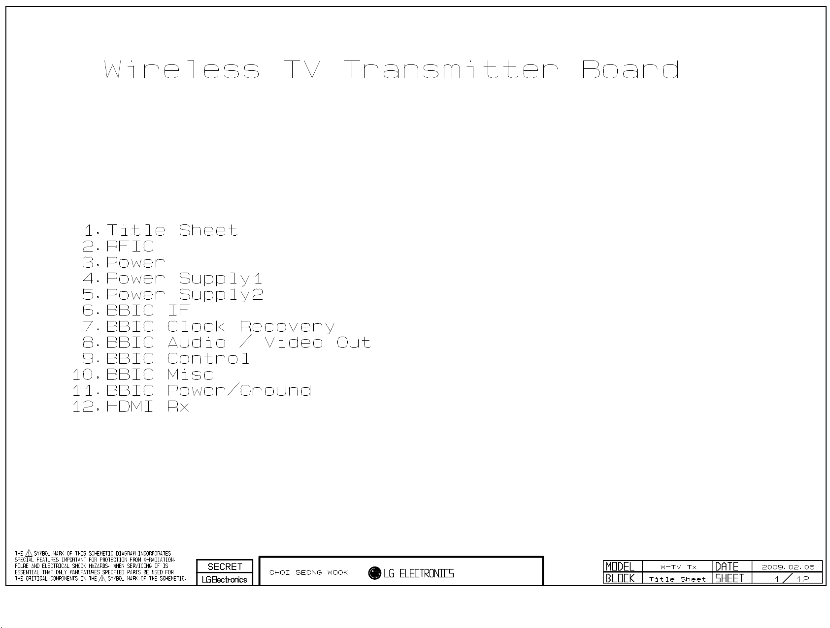
Copyright © 2009 LG Electronics. Inc. All right reserved.
Only for training and service purposes
LGE Internal Use Only
Page 37
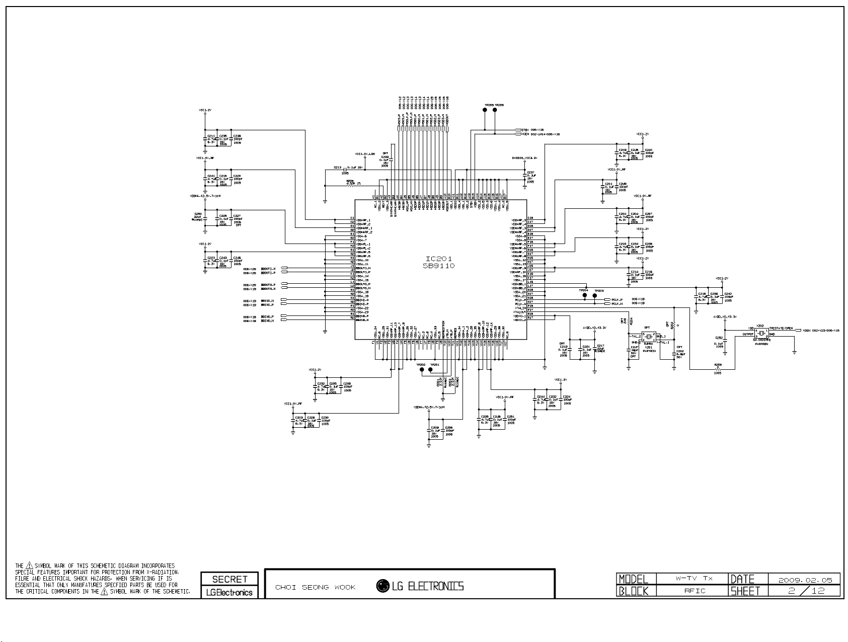
Copyright © 2009 LG Electronics. Inc. All right reserved.
Only for training and service purposes
LGE Internal Use Only
Page 38
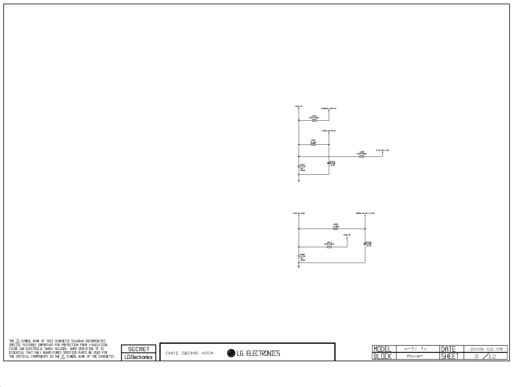
Copyright © 2009 LG Electronics. Inc. All right reserved.
Only for training and service purposes
LGE Internal Use Only
Page 39
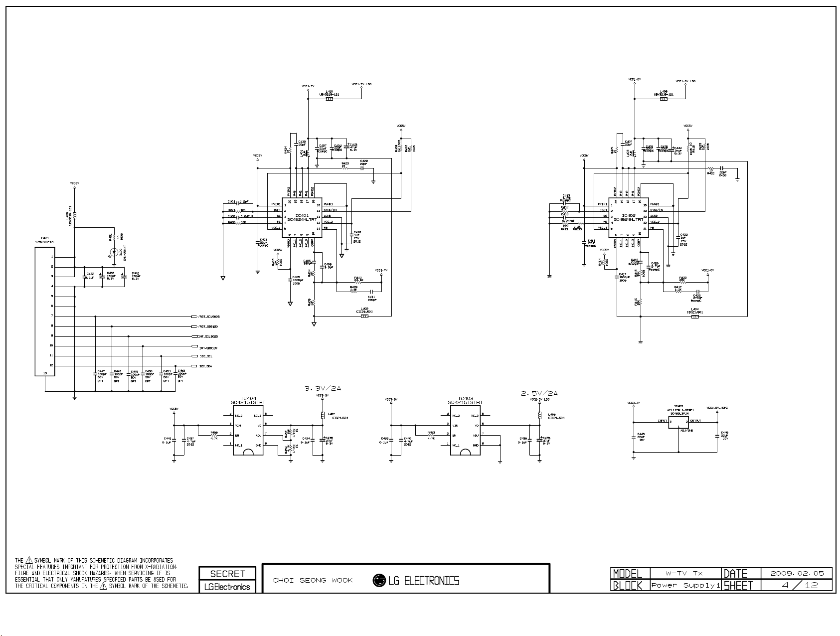
Copyright © 2009 LG Electronics. Inc. All right reserved.
Only for training and service purposes
LGE Internal Use Only
Page 40
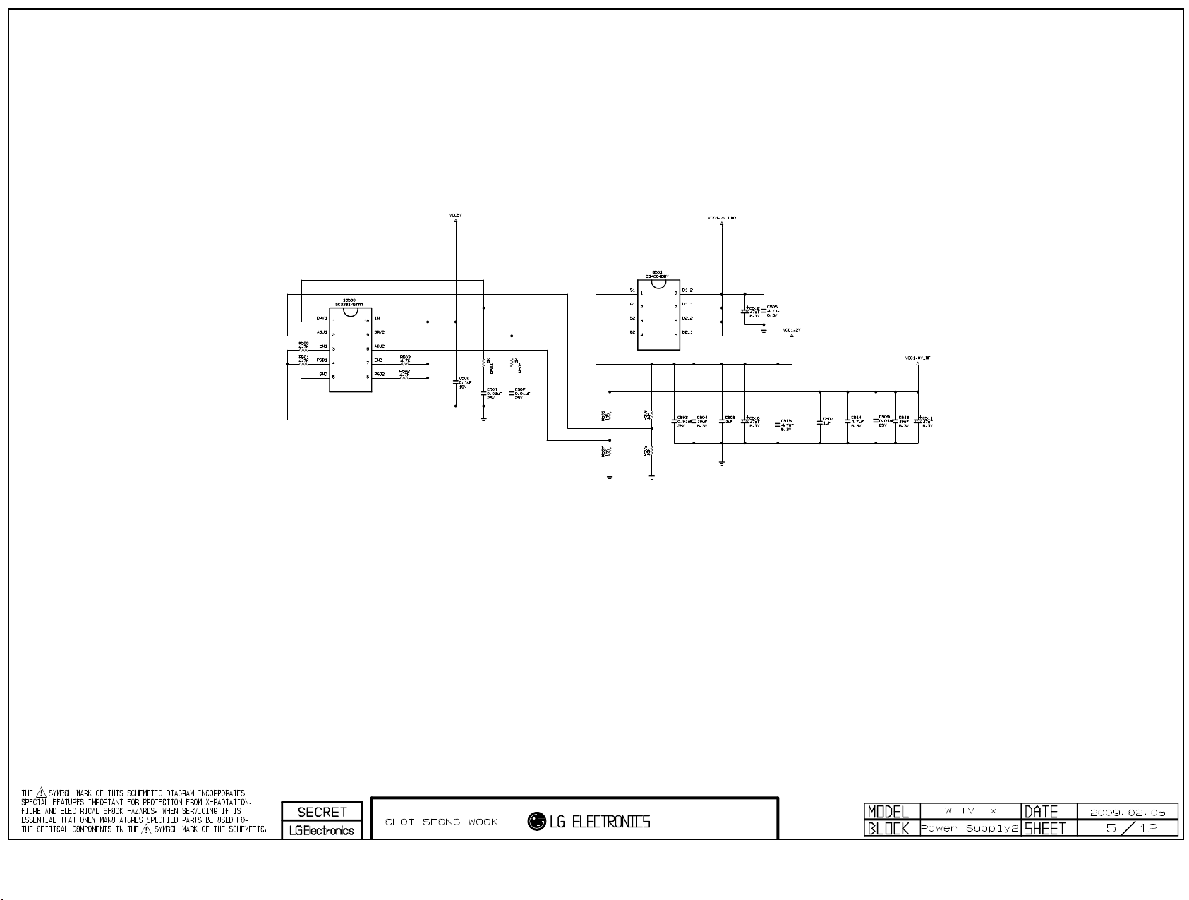
Copyright © 2009 LG Electronics. Inc. All right reserved.
Only for training and service purposes
LGE Internal Use Only
Page 41
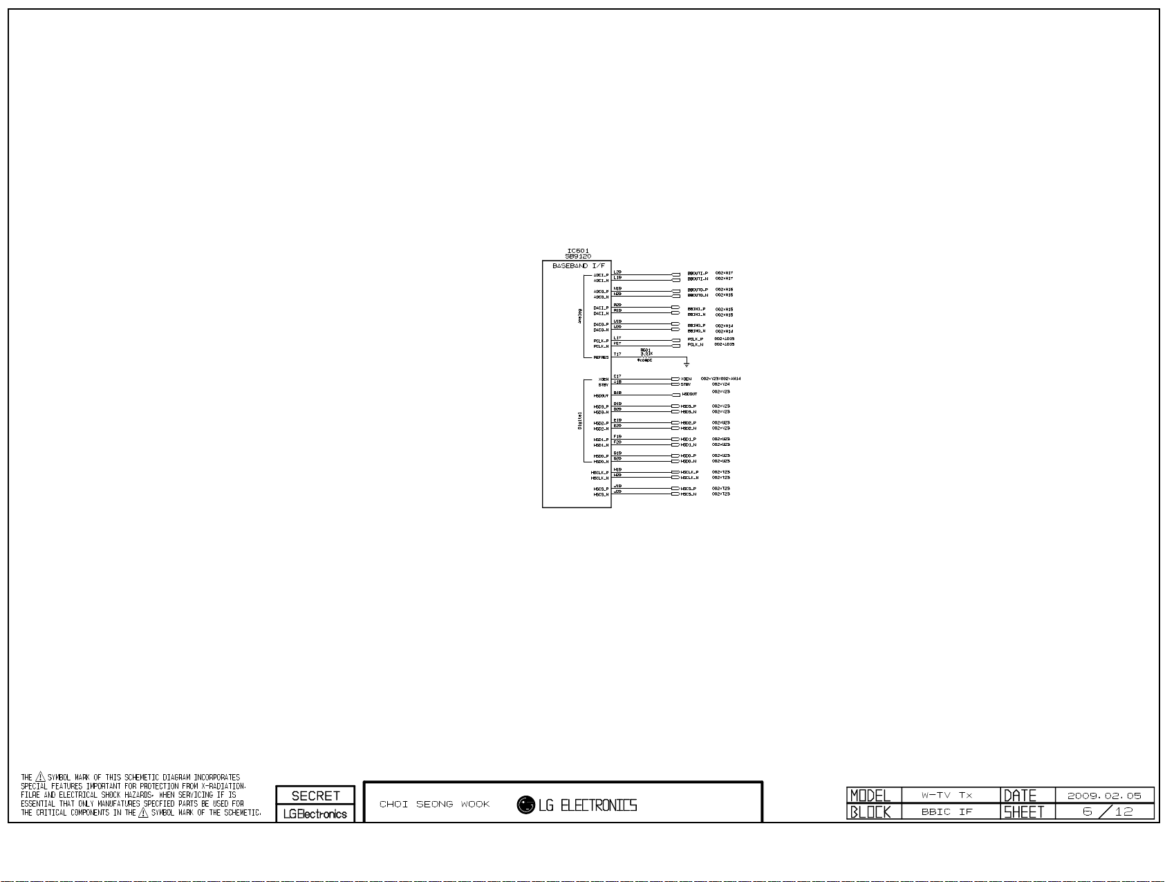
Copyright © 2009 LG Electronics. Inc. All right reserved.
Only for training and service purposes
LGE Internal Use Only
Page 42
Copyright © 2009 LG Electronics. Inc. All right reserved.
Only for training and service purposes
LGE Internal Use Only
Page 43
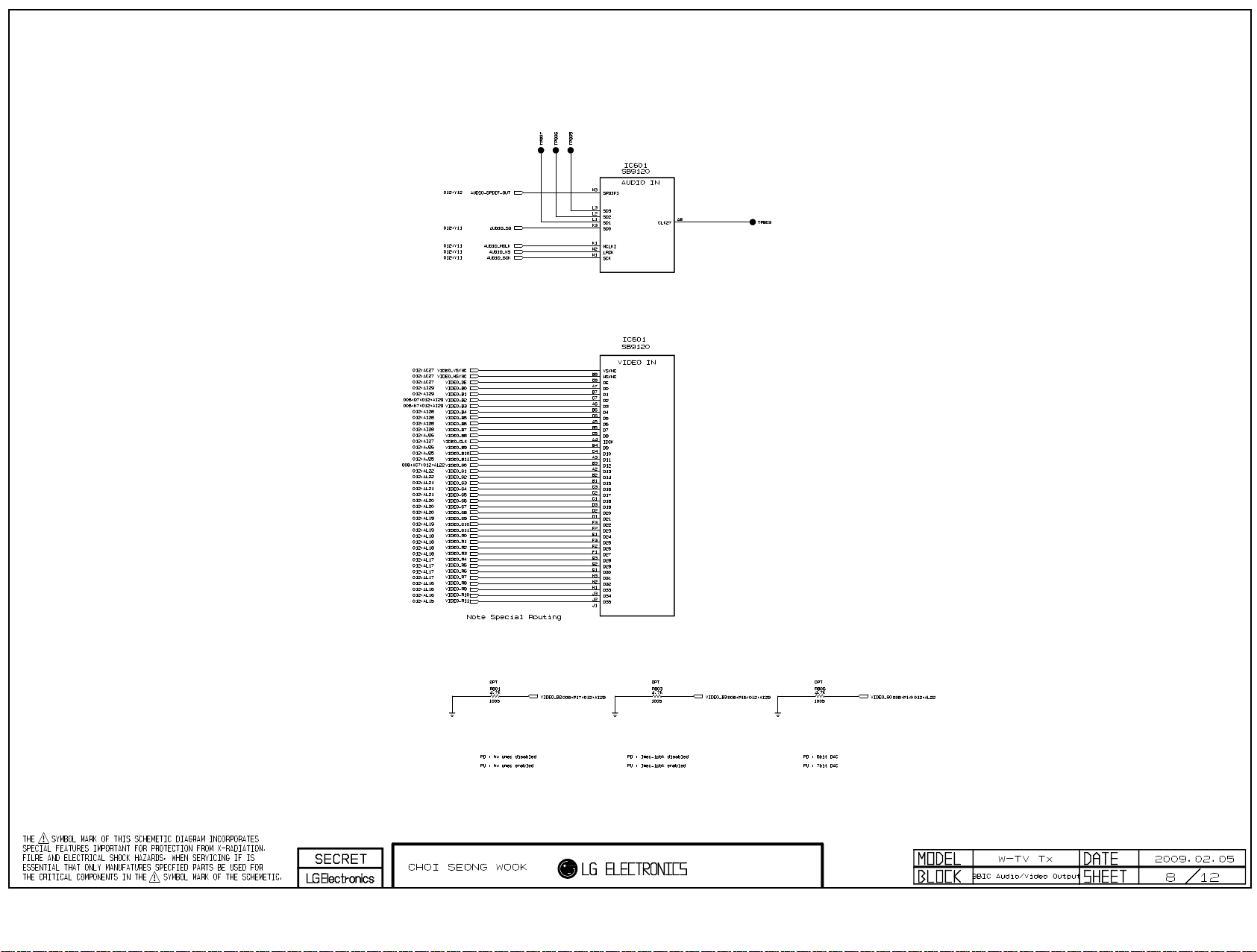
Copyright © 2009 LG Electronics. Inc. All right reserved.
Only for training and service purposes
LGE Internal Use Only
Page 44
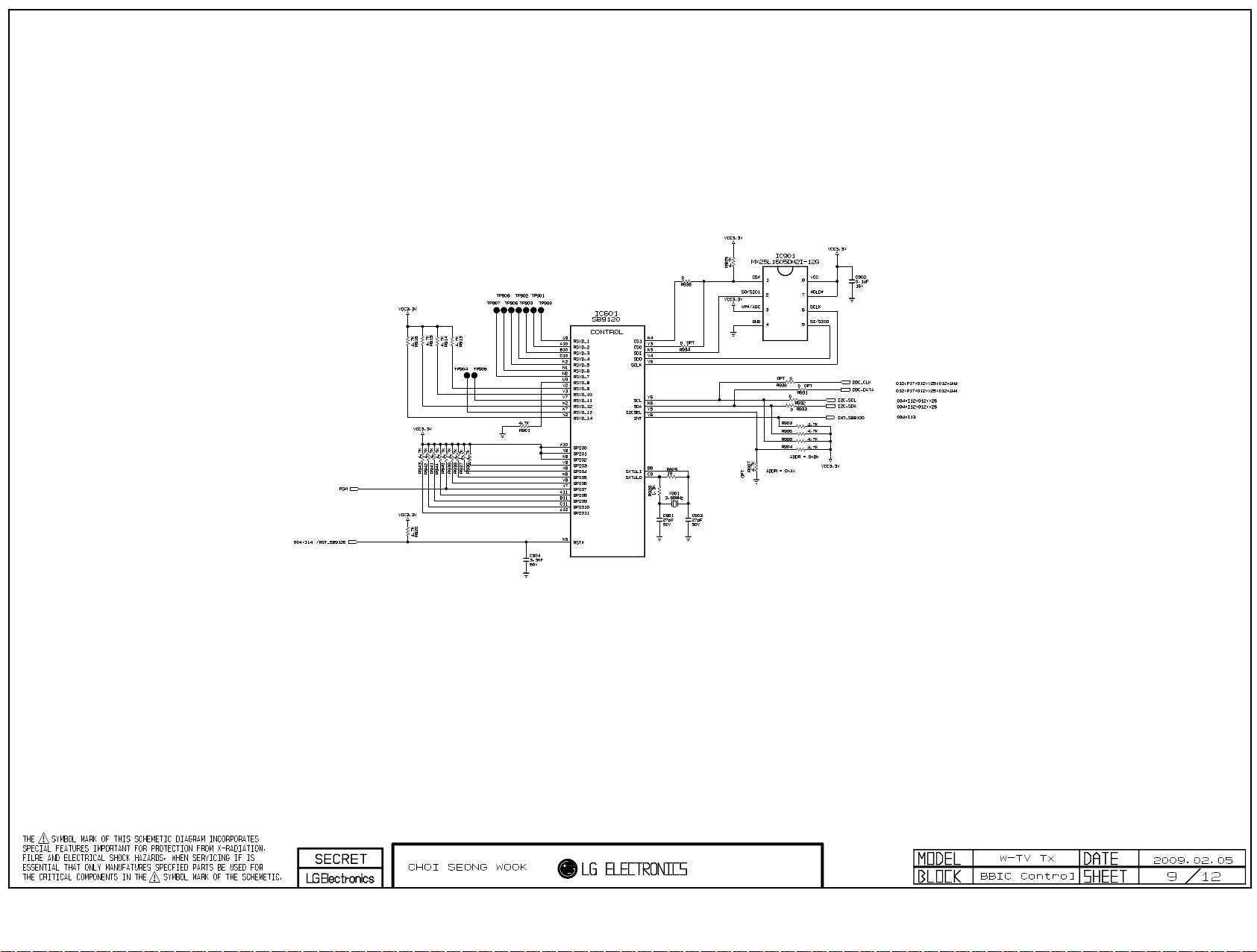
Copyright © 2009 LG Electronics. Inc. All right reserved.
Only for training and service purposes
LGE Internal Use Only
Page 45
Copyright © 2009 LG Electronics. Inc. All right reserved.
Only for training and service purposes
LGE Internal Use Only
Page 46
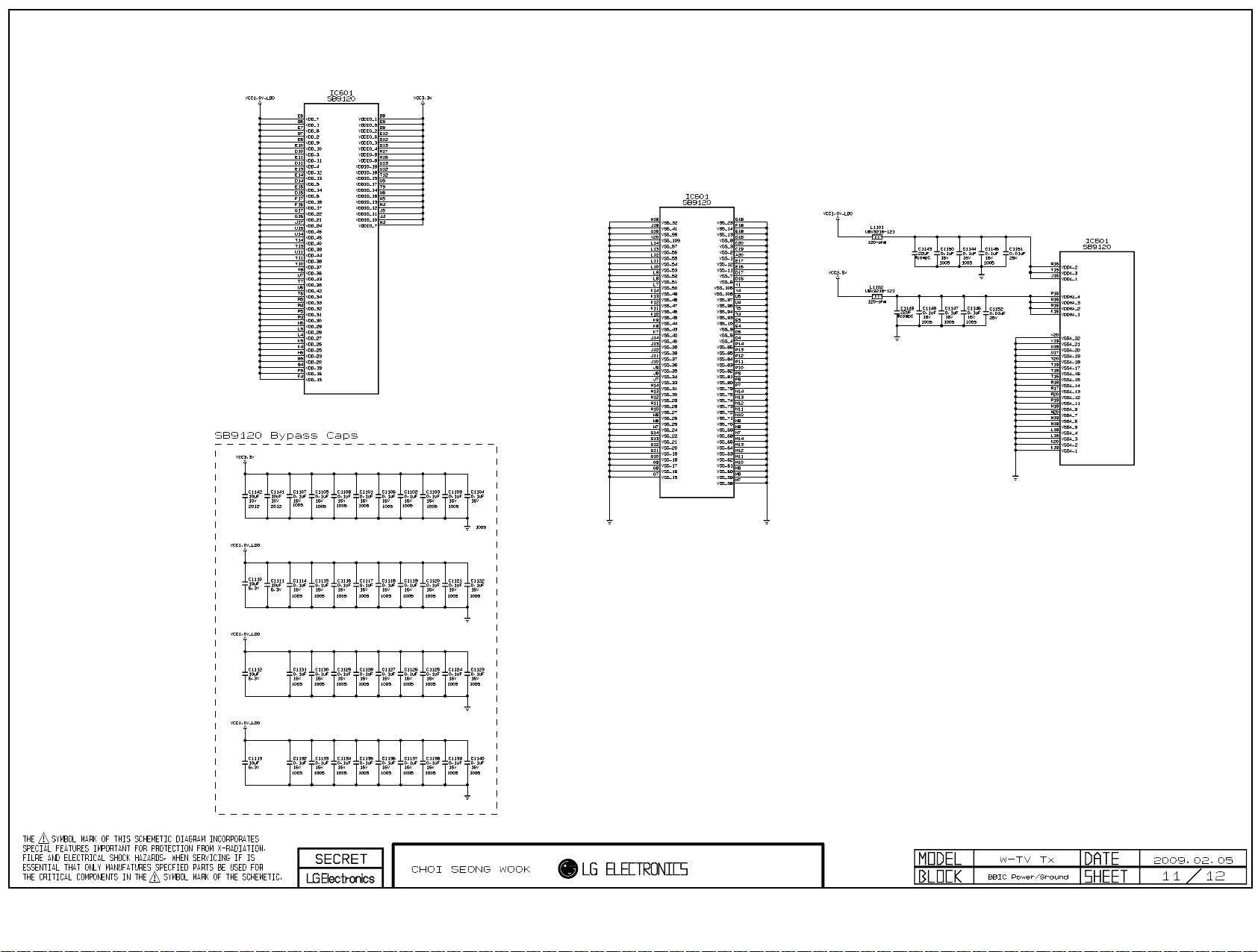
Copyright © 2009 LG Electronics. Inc. All right reserved.
Only for training and service purposes
LGE Internal Use Only
Page 47
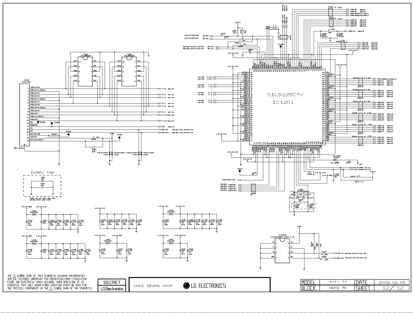
Copyright © 2009 LG Electronics. Inc. All right reserved.
Only for training and service purposes
LGE Internal Use Only
Page 48
Wireless TV Receiver Board
Copyright © 2009 LG Electronics. Inc. All right reserved.
Only for training and service purposes
LGE Internal Use Only
1.Title Sheet
2.RFIC
3.Power
4.Power Supply1
5.Power Supply2
6.BBIC IF
7.BBIC Clock Recovery
8.BBIC Audio / Video Out
9.BBIC Control
10.BBIC Misc
11.BBIC Power/Ground
12.HDMI Tx
13.uController
THE SYMBOL MARK OF THIS SCHEMETIC DIAGRAM INCORPORATES
SPECIAL FEATURES IMPORTANT FOR PROTECTION FROM X-RADIATION.
FILRE AND ELECTRICAL SHOCK HAZARDS, WHEN SERVICING IF IS
ESSENTIAL THAT ONLY MANUFATURES SPECFIED PARTS BE USED FOR
THE CRITICAL COMPONENTS IN THE SYMBOL MARK OF THE SCHEMETIC.
W-TV Rx
Title Sheet
2009.02.03
1 13
Page 49
B
Copyright © 2009 LG Electronics. Inc. All right reserved.
Only for training and service purposes
LGE Internal Use Only
A
29
28
27
26
25
G N VD AJAES AF AMAKIE L ABYJ WF ADU AOK AIQ ZR AA AG AHM XH P AL ANACOC T
24
23
22
VCC1.0V(RF)
21
R202
4.53K
C225
0.1uF
16V
1005
C227
0.1uF
16V
1005
C1
C2
D1
D2
E1
E2
F1
F2
G1
G2
H1
H2
J1
J2
K1
K2
L1
L2
M1
M2
N1
N2
P1
P2
R1
R2
1%
VDDARF_1
VDDARF_2
VDDARF_5
VDDARF_6
VSSA_6
VSSA_7
VDDAPL_1
VDDAPL_2
VDDHARF_1
VDDHARF_2
VSSA_10
VSSA_11
BBINI_N
BBINI_P
VSSA_14
VSSA_15
BBINQ_P
BBINQ_N
VSSA_18
VSSA_19
BBOUTI_N
BBOUTI_P
VSSA_22
VSSA_23
BBOUTQ_P
BBOUTQ_N
20
VCC1.2V VCC1.2V
19
C231
0.1uF
16V
1005
C236
0.1uF
16V
1005
C237
100pF
50V
1005
C230
4.7uF
6.3V
1608
C235
22uF
10V
3216
C238
0.1uF
16V
1005
C232
C233
0.1uF
100pF
16V
50V
1005
1005
BBINI_N6:Y17
BBINI_P6:Y17
BBINQ_P6:Y16
BBINQ_N6:Y16
BBOUTI_N6:Y18
BBOUTI_P6:Y18
BBOUTQ_P6:Y18
BBOUTQ_N6:Y17
VCC1.2V
C224
100pF
50V
1005
VCC1.2V
C228
100pF
50V
1005
C229
100pF
50V
18
17
16
15
14
13
12
11
10
9
8
1005
VDD_+2.5V_RxicM
C234
100pF
50V
1005
OPT
VCC1.0V(RF)
C246
4.7uF
6.3V
1608
C239
0.1uF
16V
1005
A1
B1
A2
NC_1
REXT
VSSA_2
VSSA_24T1NC_6U1VSSA_25T2VSSA_31U2VDDARF_15T3VDDARF_19U3VDDARF_16T4VDDARF_20U4VSSA_26T5VSSA_32U5VSSA_27T6NC_7U6NC_3T7NC_8U7NC_4T8VSSA_33U8NC_5T9REFRESTRIMU9ATB_N
C226
4.7uF
6.3V
1608
OPT
B2
B3
VSSA_3
SYNTHCAPPA3SYNTHCAPN
HSCS_P 6:Y11
HSCS_N 6:Y10
B4
HSCSPA4HSCSN
6:Y11
HSCLK_P
HSCLKPA5HSCLKN
6:Y11
HSCLK_N
B5
VDD_+2.5V_RxicM
HSD0_P 6:Y12
HSD0_N 6:Y12
HSD1_P 6:Y12
HSD1_N 6:Y12
HSD2_P 6:Y13
HSD2_N 6:Y13
HSD3_P 6:Y14
HSD3_N 6:Y13
B9
HSD0PA6HSD0NB6HSD1PA7HSD1NB7HSD2PA8HSD2NB8HSD3PA9HSD3N
IC201
SB9111
R201
3.01K
C240
C241
100pF
0.1uF
50V
16V
1005
1005
OPT
HSDOUT 6:Y14
A10
HSDOUT
T10
TP302
1%
1005
B10
U10
R203
A11
VDD_1
ATB_P
T11
TP301
3.01K
B11
VDDIO
VSS_4
REFRES
VSSA_34
U11
1005
A12
VSS_1
VDDHA_1
T12
1%
6:Y14
RFMODE_STBY
B12
A13
STBY
VDD_2
VDDHA_2
VSSA_28
U12
T13
AL12;6:Y15
XO_EN
B13
A14
B14
XOEN
VSS_2
VSSA_35
VDDARF_17
U13
T14
U14
A15
B15
A16
VSS_5
VSS_3
VSS_6
VDDARF_21
VDDARF_18
VDDARF_22
T15
U15
T16
B16
A17
VSSA_1
VSSA_4
VSSA_29
VSSA_36
U16
T17
B17
NC_2
VSSA_5
VDDARF_10
VDDARF_11
VDDARF_12
VDDARF_13
VDDARF_14
VSSA_30
NC_9
U17
VDDARF_3
VDDARF_4
VDDARF_7
VDDARF_8
VSSA_8
VSSA_9
VDDARF_9
VSSA_12
VSSA_13
VSSA_16
VSSA_17
VDDABB_1
VDDABB_2
VSSA_20
VSSA_21
PCLK_P
PCLK_N
XTALIN
XTALOUT
VDDXO_1
VDDXO_2
C16
C17
D16
D17
E16
E17
F16
F17
G16
G17
H16
H17
J16
J17
K16
K17
L16
L17
M16
M17
N16
N17
P16
P17
R16
R17
1005
C223
100pF
50V
1005
C219
100pF
50V
DVDDIO_VCC3.3V
C203
0.1uF
16V
1005
VCC1.2V
C221
0.1uF
16V
1005
VCC1.2V
C222
0.1uF
16V
1005
C220
4.7uF
6.3V
1608
C201
100pF
50V
1005
C214
100pF
50V
1005
OPT
VCC1.2V
C202
C204
4.7uF
0.1uF
6.3V
16V
1005
1608
PCLK_P 6:Y16
PCLK_N 6:Y16
AVDD_XO_+3.3V
C215
C216
0.1uF
22uF
10V
16V
3216
1005
C206
100pF
50V
1005
C208
100pF
50V
1005
R206
1005
VCC1.2V
VCC1.2V
0
C205
0.1uF
16V
1005
C207
0.1uF
16V
1005
DVDDIO_VCC3.3V
C244
0.1uF
1005
C213
100pF
50V
1005
OUTPUT
C211
100pF
50V
1005
VCC1.2V
VDD
54.0000MHz
C212
0.1uF
16V
1005
X203
4
3
PARTRON
C209
0.1uF
16V
1005
C218
100pF
50V
1005
TRISTATE/OPEN
1
GND
2
VCC1.2V
C217
0.1uF
16V
1005
C210
4.7uF
6.3V
1608
VCC1.2V
C245
4.7uF
6.3V
1608
XO_EN V22;6:Y15
7
6
5
4
3
2
THE SYMBOL MARK OF THIS SCHEMETIC DIAGRAM INCORPORATES
SPECIAL FEATURES IMPORTANT FOR PROTECTION FROM X-RADIATION.
FILRE AND ELECTRICAL SHOCK HAZARDS, WHEN SERVICING IF IS
1
ESSENTIAL THAT ONLY MANUFATURES SPECFIED PARTS BE USED FOR
THE CRITICAL COMPONENTS IN THE SYMBOL MARK OF THE SCHEMETIC.
W-TV Rx
RFIC
2009.02.03
2 13
Page 50
A G N VD AJAES AF AMAKIE L ABB YJ WF ADU AOK AIQ ZR AA AG AHM XH P AL ANACOC T
Copyright © 2009 LG Electronics. Inc. All right reserved.
Only for training and service purposes
LGE Internal Use Only
29
28
27
26
25
24
23
22
21
20
19
18
17
16
15
14
13
12
11
VCC3.3V
VCC3.3V
VCC2.5V
VCC3.3V
C301
10uF
16V
3216
C302
10uF
16V
3216
C309
4.7uF
10V
2012
L302
CIC21J601
3.3uH
L303
3.3uH
L304
L312
CIC21J601
DVDDIO_VCC3.3V
AVDD_XO_+3.3V
VDD_+2.5V_RxicM
IOVCC3.3V
VCC1.8VH
C306
4.7uF
2012
10V
L308
CIC21J601
AVCC1.8V
VCC3.3V
L311
CIC21J601
C310
10uF
16V
3216
C311
10uF
16V
3216
AZ1117R-1.8TRE1
SOT89_3PIN
INPUT
3
IC301
1
ADJ/GND
VCC1.8VH
OUTPUT
2
C312
10uF
16V
3216
10
9
VCC1.8VH
8
C308
4.7uF
7
6
5
4
3
2
THE SYMBOL MARK OF THIS SCHEMETIC DIAGRAM INCORPORATES
2012
10V
SPECIAL FEATURES IMPORTANT FOR PROTECTION FROM X-RADIATION.
FILRE AND ELECTRICAL SHOCK HAZARDS, WHEN SERVICING IF IS
1
ESSENTIAL THAT ONLY MANUFATURES SPECFIED PARTS BE USED FOR
THE CRITICAL COMPONENTS IN THE SYMBOL MARK OF THE SCHEMETIC.
CVCC1.8V PVCC1.8V
L310
CIC21J601
VCC1.8VH
C307
4.7uF
2012
10V
L309
CIC21J601
W-TV Rx
Power
2009.02.03
3 13
Page 51
A G N VD AJAES AF AMAKIE L ABB YJ WF ADU AOK AIQ ZR AA AG AHM XH P AL ANACOC T
Copyright © 2009 LG Electronics. Inc. All right reserved.
Only for training and service purposes
LGE Internal Use Only
29
28
27
26
25
24
23
22
21
C415
20
19
18
17
16
15
R406
C411 0.047uF
R415
AGND0
1.2pF
10K
12K
1005
1005
1005
C414
3216
10uF
16V
VCC5V
VCC5V
R414
PVIN1
ISET
VCC_1
10K
SS
FS
1005
1.4V/3.5A
VCC1.4V
2uH
L404
1005
1005
R420
C421
10
22pF
PH118PH219PH320PVIN2
IC402
SC4624MLTRT
7
8
6
NC_19NC_310COMP
NC_2
PGOOD
C416
330pF
1608
C413
1000pF
1005
17
R411
18K
R405
10K
1
2
3
4
5
C408
22uF
10V
3216
NR8040T2R0N
R421
10
PGND2
16
PGND1
15
SYNC/EN
14
AGND
13
VCC_2
12
FB
11
3.3pF
1608
1005
1005
C409
C426
47uF
6.3V
7343
22pF
C423
AGND0
1005
R407
1.8K
1608
C412
1uF
10V
1608
R416
24.9K1%
1005
L405
CIC21J601
C410
220pF
1608
VCC5V
R412101005
R413
10K
1005
C420
R417
C401
R418
AGND1
1.2pF
10K
0.047uF
47K
1005
1005
1005
1005
C419
3216
10uF
16V
VCC5V
VCC5V
R403
10K
PVIN1
ISET
VCC_1
SS
FS
1005
1
2
3
4
5
1.0V/3A
VCC1.0V
1005
1005
R419
C422
10
22pF
IC401
SC4624MLTRT
7
8
6
NC_19NC_310COMP
NC_2
PGOOD
C403
1000pF
1005
L403
2uH
NR8040T2R0N
PGND217PH118PH219PH320PVIN2
16
15
14
13
12
11
270pF
C404
R404
30K
1005
R401
20K
1005
C407
10uF
16V
3216
1%
R422
1005
10
PGND1
SYNC/EN
AGND
VCC_2
FB
C406
2.7pF
1005
C418
47uF
6.3V
7343
22pF
C424
AGND1
1005
R408
1.2K
1005
C402
1uF
10V
1608
R410
24.9K
1005
L406
CIC21J601
C405
270pF
VCC1.0VVCC1.4V
VCC5V
R402
10
1005
R409
10K
1005
14
13
12
11
VCC5V
10
C428
9
8
7
6
5
4
C427
0.1uF
22uF
10V
16V
3216
R423
4.7K
4
3
2
1
AGND0
IC403
SC4215ISTRT
NC_2
VIN
EN
NC_1
NC_3
3.3V/2A 2.5V/2A
C431
0.1uF
VCC3.3V
16V
C430
22uF
10V
3216
R426
4.7K
5
6
VO
7
ADJ
8
GND
R424
R425
15K
4.7K
1/10W
1/10W
1%
C425
0.1uF
16V
1%
C417
47uF
6.3V
7343
L407
CIC21J601
IC404
SC4215ISTRT
4
NC_2
3
VIN
2
EN
1
NC_1
AGND1
NC_3
VCC2.5VVCC3.3V
5
6
VO
7
ADJ
8
GND
C432
0.1uF
16V
C429
47uF
6.3V
7343
L408
CIC21J601
3
2
THE SYMBOL MARK OF THIS SCHEMETIC DIAGRAM INCORPORATES
SPECIAL FEATURES IMPORTANT FOR PROTECTION FROM X-RADIATION.
FILRE AND ELECTRICAL SHOCK HAZARDS, WHEN SERVICING IF IS
1
ESSENTIAL THAT ONLY MANUFATURES SPECFIED PARTS BE USED FOR
THE CRITICAL COMPONENTS IN THE SYMBOL MARK OF THE SCHEMETIC.
W-TV Rx
Power Supply1
2009.02.03
4 13
Page 52
A G N VD AJAES AF AMAKIE L ABB YJ WF ADU AOK AIQ ZR AA AG AHM XH P AL ANACOC T
Copyright © 2009 LG Electronics. Inc. All right reserved.
Only for training and service purposes
LGE Internal Use Only
29
28
27
26
25
24
23
22
21
20
DRV1
ADJ1
PGD1
EN1
GND
IC501
SC338IMSTRT
1
2
3
4
5
19
18
17
16
15
14
13
12
11
10
VCC3.3V
R507
4.7K
1005
4.7K
1005
R505
VCC5V
IN
10
DRV2
9
ADJ2
8
EN2
7
PGD2
6
C505
0.1uF
16V
1005
R508
4.7K
1005
R506
4.7K
1005
VCC3.3V
R509
2K
1005
C506
0.01uF
25V
1005
R503
2K
1005
C504
0.01uF
25V
1005
1005
C510
1uF
6.3V
VCC1.0V(RF)
C508
10uF
6.3V
1608
C509
0.1uF
16V
1005
C511
47uF
6.3V
7343
VCC1.2V
R504
12K1%1005
R510
10K
1005
VCC1.4V
Q501
SI4804BDY
S1
1
@compC
G1
2
S2
3
G2
4
1%
D1_2
8
D1_1
7
D2_2
6
D2_1
5
C503
4.7uF
10V
2012
R501
15K1%1005
R502
10K
1005
C513
0.1uF
16V
1005
1%
C501
1uF
6.3V
1005
C514
47uF
6.3V
7343
C502
10uF
6.3V
1608
C507
0.1uF
16V
1005
C512
47uF
6.3V
7343
9
8
7
6
5
4
3
2
THE SYMBOL MARK OF THIS SCHEMETIC DIAGRAM INCORPORATES
SPECIAL FEATURES IMPORTANT FOR PROTECTION FROM X-RADIATION.
FILRE AND ELECTRICAL SHOCK HAZARDS, WHEN SERVICING IF IS
1
ESSENTIAL THAT ONLY MANUFATURES SPECFIED PARTS BE USED FOR
THE CRITICAL COMPONENTS IN THE SYMBOL MARK OF THE SCHEMETIC.
W-TV Rx
Power Supply2
2009.02.03
5 13
Page 53
A G ND AJAE AF AMAKIE L ABB YJF AD AOAIZ AA AG AHM XH P AL ANACOC
Copyright © 2009 LG Electronics. Inc. All right reserved.
Only for training and service purposes
LGE Internal Use Only
29
28
27
26
25
24
23
22
21
20
19
18
17
IC601
SB9121
Baseband I/F
Digital Analog
ADCI_P
ADCI_N
ADCQ_P
ADCQ_N
DACI_P
DACI_N
DACQ_P
DACQ_N
PCLK_P
PCLK_N
REFRES
XOEN
STBY
HSDOUT
HSD3_P
HSD3_N
HSD2_P
HSD2_N
HSD1_P
HSD1_N
HSD0_P
HSD0_N
HSCLK_P
HSCLK_N
HSCS_P
HSCS_N
R22
R21
U21
U22
L22
L21
N21
N22
N19
M19
R601
3.01K
H19
1005
1%
E20
D20
F20
D21
D22
E21
E22
F21
F22
G21
G22
H21
H22
J21
J22
BBOUTI_P 2:N14
BBOUTI_N 2:N15
BBOUTQ_P 2:N14
BBOUTQ_N 2:N14
BBINI_P 2:N16
BBINI_N 2:N16
BBINQ_P 2:N15
BBINQ_N 2:N15
PCLK_P 2:AA15
PCLK_N 2:AA14
XO_EN 2:V22;2:AL12
RFMODE_STBY 2:V22
HSDOUT 2:U22
HSD3_P 2:T22
HSD3_N 2:T22
HSD2_P 2:T22
HSD2_N 2:T22
HSD1_P 2:S22
HSD1_N 2:T22
HSD0_P 2:S22
HSD0_N 2:S22
HSCLK_P 2:S22
HSCLK_N 2:S22
HSCS_P 2:R22
HSCS_N 2:R22
7
6
5
4
3
2
THE SYMBOL MARK OF THIS SCHEMETIC DIAGRAM INCORPORATES
SPECIAL FEATURES IMPORTANT FOR PROTECTION FROM X-RADIATION.
FILRE AND ELECTRICAL SHOCK HAZARDS, WHEN SERVICING IF IS
1
ESSENTIAL THAT ONLY MANUFATURES SPECFIED PARTS BE USED FOR
THE CRITICAL COMPONENTS IN THE SYMBOL MARK OF THE SCHEMETIC.
W-TV Rx
BBIC IF
2009.02.03
6 13
Page 54
A G N VD AJAES AF AMAKIE L ABB YJ WF ADU AOK AIQ ZR AA AG AHM XH P AL ANACOC T
Copyright © 2009 LG Electronics. Inc. All right reserved.
Only for training and service purposes
LGE Internal Use Only
29
28
27
26
25
VCC3.3V
24
VCC3.3V
23
22
21
20
19
18
17
IC601
SB9121
Clock Recovery
VDAC_SDA
VDAC_SCL
VCLK27
VCLK
ACLK
ACLK27
C10
A9
C11
B9
B13
A13
R701
4.7K
1005
VCLK_27 Z18
VCLK_IN AF21
ACLK_IN AF9
ACLK_27 Z6
R705
4.7K
1005
R702
4.7K
1005
IC701
AD5622BKSZ-2500RL7
ADDR
1
SCL
2
SDA
3
R720
4.7K
1005
VCC3.3V
VCC1.8VH
R706
1.2K
L701
CIC21J601
C702
1nF
50V
1005
1005
OPT
VOUT
6
GND
5
VDD
4
C711
4.7uF
R703
1K
1005
C701
0.1uF
16V
1005
6.3V
L703
CIC21J601
C713
4.7uF
6.3V
R707
4.7K
C705
0.1uF
16V
1005
OPT
1005
VCC3.3V
C703
0.1uF
16V
1005
XIN/CLK
VDDOUT_1
22
R721
VDD
VCTR
GND_1
1005
X701
27MHz
IC702
GND_2
4
1
X-TAL_2
2
3
16
15
14
13
12
11
10
9
X-TAL_1
GND_1
MAIN: SUNNY / SUB: PARTRON
CDCE925PWR
1
S0
2
3
4
5
6
Y4
7
Y5
8
VCLK_27 K17
XOUT
S1/SDA
S2/SCL
Y1
GND_2
Y2
Y3
VDDOUT_2
0.1uF
1005
C704
VCC3.3V
R708
4.7K
R709
4.7K
1005
1005
GPIO6 9:I14
R704
47
1005
C714
150pF
50V
VCC3.3V
16V
GPIO5 9:I14
VCLK_IN K17
C715
150pF
50V
OPT
A14
ADAC_SDA
C13
ADAC_SCL
VCC3.3V
R719
4.7K
1005
OPT
IC703
R710
4.7K
1005
4.7K
1005
R715
4.7K
1005
R716
3
AD5622BKSZ-2500RL7
ADDR
1
SCL
2
SDA
3
VOUT
6
GND
5
VDD
4
C712
1uF
R711
14K
1005
C709
0.1uF
16V
1005
6.3V
L704
CIC21J601
VCC3.3V
VCC1.8VH
R712
16K
1K
R723
L702
CIC21J601
1%
1005
1%
1005
OPT
C708
0.1uF
16V
1005
C716
4.7uF
6.3V
VCC3.3V
R717
4.7K
C707
0.1uF
16V
1005
OPT
1005
VCC3.3V
C706
0.1uF
16V
1005
XIN/CLK
VDDOUT_1
22
R722
VDD
VCTR
GND_1
1005
X702
27MHz
IC704
GND_2
4
1
X-TAL_2
2
3
XOUT
16
S1/SDA
15
S2/SCL
14
Y1
13
GND_2
12
Y2
11
Y3
10
VDDOUT_2
9
X-TAL_1
GND_1
MAIN: SUNNY / SUB: PARTRON
CDCE925PWR
1
S0
2
3
4
5
6
Y4
7
Y5
8
ACLK_27 K15
C710
0.1uF
1005
VCC3.3V
R713
4.7K
1005
R714
4.7K
1005
GPIO4 9:I14
R718
22
1005
VCC3.3V
16V
GPIO3 9:I14
ACLK_IN K15
2
THE SYMBOL MARK OF THIS SCHEMETIC DIAGRAM INCORPORATES
SPECIAL FEATURES IMPORTANT FOR PROTECTION FROM X-RADIATION.
FILRE AND ELECTRICAL SHOCK HAZARDS, WHEN SERVICING IF IS
1
ESSENTIAL THAT ONLY MANUFATURES SPECFIED PARTS BE USED FOR
THE CRITICAL COMPONENTS IN THE SYMBOL MARK OF THE SCHEMETIC.
W-TV Rx
BBIC Clock Recovery
2009.02.03
7 13
Page 55
A G N VD AJAES AF AMAKIE L ABB YJ WF ADU AOK AIQ ZR AA AG AHM XH P AL ANACOC T
Copyright © 2009 LG Electronics. Inc. All right reserved.
Only for training and service purposes
LGE Internal Use Only
29
28
IC601
SB9121
Audio I/O
TP803
C12
CLK27
SPDIFO
MCLKO
LRCK
MUTE
P1
M3
SD3
M2
SD2
M1
SD1
L1
SD0
L3
N2
N1
SCK
P2
TP804
TP805
TP806
TP807
AR806 22
TP808
2010_A4
AUDIO_SD0 12:E17
AUDIO_MCLK 12:E17
AUDIO_WS 12:E16
AUDIO_SCLK 12:E16
Note Special Routing
IC601
SB9121
Video Out
ODCK
HSYNC
VSYNC
47
47
2010_A4
2010_A4
2010_A4
2010_A4
2010_A4
2010_A4
2010_A4
2010_A4
2010_A4
2010_A4
VIDEO_D35 12:S14
VIDEO_D34 12:S15
VIDEO_D33 12:S15
VIDEO_D32 12:S15
VIDEO_D31 12:S15
VIDEO_D30 12:S15
VIDEO_D29 12:S16
VIDEO_D28 12:S16
VIDEO_D27 12:S17
VIDEO_D26 12:S17
VIDEO_D25 12:S17
VIDEO_D24 12:S17
VIDEO_D23 12:S17
VIDEO_D22 12:S18
VIDEO_D21 12:S18
VIDEO_D20 12:S18
VIDEO_D19 12:S18
VIDEO_D18 12:N23
VIDEO_D17 12:N23
VIDEO_D16 12:N23
VIDEO_D15 12:M23
VIDEO_D14 12:M23
VIDEO_D13 12:M23
VIDEO_D12 AA6;12:M23
VIDEO_D11 12:M23
VIDEO_D10 12:L23
VIDEO_D09 12:L23
VIDEO_D08 12:K23
VIDEO_D07 12:K23
VIDEO_D06 12:K23
VIDEO_D05 12:K23
VIDEO_D04 12:K23
VIDEO_D03 U6;12:J23
VIDEO_D02 P6;12:J23
VIDEO_D01 12:J23
VIDEO_D00 12:J23
VIDEO_DE 12:E18
VIDEO_HSYNC 12:E18
VIDEO_VSYNC 12:E18
C800
150pF
50V
R804 47
OPT
VIDEO_CLK 12:L23
K1
D35
K2
D34
K3
D33
J1
D32
J2
D31
J3
D30
H1
D29
H2
D28
H3
D27
G1
D26
G2
D25
G3
D24
F1
D23
F2
D22
F3
D21
E1
D20
E2
D19
E3
D18
D1
D17
D2
D16
D3
D15
C1
D14
C3
D13
A3
D12
C4
D11
B4
D10
A4
D9
C5
B5
D8
A5
D7
C6
D6
B6
D5
A6
D4
C7
D3
B7
D2
A7
D1
C8
D0
B8
DE
A8
C9
AR801 47
AR802 47
AR803 47
AR804
AR805 47
AR811 47
AR807
AR808 47
AR809 47
AR810 47
4
3
2
THE SYMBOL MARK OF THIS SCHEMETIC DIAGRAM INCORPORATES
SPECIAL FEATURES IMPORTANT FOR PROTECTION FROM X-RADIATION.
FILRE AND ELECTRICAL SHOCK HAZARDS, WHEN SERVICING IF IS
1
ESSENTIAL THAT ONLY MANUFATURES SPECFIED PARTS BE USED FOR
THE CRITICAL COMPONENTS IN THE SYMBOL MARK OF THE SCHEMETIC.
R801
4.7K
1005
R802
4.7K
OPT
1005
OPT
PD : lmac_1pbk disabledPD : hw umac disabled
R803
4.7K
1005
OPT
PD : 6bit DAC
VIDEO_D12 X12;12:M23VIDEO_D02 X9;12:J23 VIDEO_D03 X9;12:J23
W-TV Rx
BBIC Audio/Video Output
2009.02.03
8 13
Page 56
A G N VD AJAES AF AMAKIE L ABB YJ WF ADU AOK AIQ ZR AA AG AHM XH P AL ANACOC T
Copyright © 2009 LG Electronics. Inc. All right reserved.
Only for training and service purposes
LGE Internal Use Only
29
28
27
26
25
24
23
TP902
C903
30pF
1005
VCC3.3V
R906
4.7K
VCC3.3V
1005
SO/SIO1
WP#/AGC
IC901
MX25L1605DM2I-12G
CS#
1
2
3
GND
4
@compC
R909 4.7K
R908 4.7K
R907 4.7K
R922 4.7K
ADDR = 0xBx
OPT
R911
4.7K
1005
ADDR = 0xAx
VCC3.3V
VCC
8
HOLD#
7
SCLK
6
SI/SIO0
5
1005
1005OPT
OPT
1005
1005
VCC3.3V
C902
0.1uF
16V
1005
I2C_SCL 12:N7;12:Z14;13:W14;13:AH10
I2C_SDA 12:N7;12:Z14;13:W14;13:AH10
BB_INTN 13:W16;13:AH9
22
21
20
19
18
17
16
15
14
13
12
11
VCC3.3V
R92 3
4.7 K
R92 6
4.7 K
R92 4
R92 5
TP907
TP910
TP909
TP908
TP911
TP913
TP912
TP914
TP915
GPIO67:AF22
GPIO57:AF22
GPIO47:AF10
GPIO37:AF10
1005
4.7 K
4.7 K
1005
1005
1005
R92 7
4.7 K
R92 8
1005
13:L9;13:AH8
VCC3.3V
IC601
L2
N3
V3
W2
W3
Y2
Y3
Y9
RSVD_1
RSVD_2
RSVD_3
RSVD_4
RSVD_5
RSVD_6
RSVD_7
RSVD_8
RSVD_9
GPIO[15]
GPIO[14]
GPIO[13]
GPIO[12]
GPIO[11]
GPIO[10]
GPIO[9]
GPIO[8]
GPIO[7]
GPIO[6]
GPIO[5]
GPIO[4]
GPIO[3]
GPIO[2]
GPIO[1]
GPIO[0]
RST#
SB9121
Control
SCLK
I2CSEL
VSS_130
SXTALI
SXTALO
Y6
CS1
AA4
CS0
Y4
SDI
Y5
SDO
AA5
AB6
SCL
AA7
SDA
Y8
AB5
INT
Y7
B12
A12
1005
R913
4.7K
4.7 K
1005
R914
1005
4.7K
1005
TP903
TP904
C904
3.3nF
50V
AA10
AB10
AA8
AB7
B11
A11
A10
B10
B15
C14
A15
B14
AB8
AA9
Y10
AB9
Y11
AA6
TP905
TP906
R903
4.7K
1005
R93 1
4.7 K
R93 3
4.7 K
1005
R93 5
4.7 K
1005
1005
VCC3.3V
R936
4.7K
1005
R915
4.7K
R916
4.7K
1005
4.7 K
1005
R92 9
4.7 K
R93 4
4.7 K
1005
BB_RSTN
1005
R93 2
R93 0
4.7 K
1005
R92001005
SPI_CS0N
R919
1M 1%
1005
R910
1K1%1005
R921
1005
X901
300 1%
3.68MHz
C901
30pF
1005
Crystal matching
27pF -> 30pF
10
9
8
7
6
5
4
3
2
THE SYMBOL MARK OF THIS SCHEMETIC DIAGRAM INCORPORATES
SPECIAL FEATURES IMPORTANT FOR PROTECTION FROM X-RADIATION.
FILRE AND ELECTRICAL SHOCK HAZARDS, WHEN SERVICING IF IS
1
ESSENTIAL THAT ONLY MANUFATURES SPECFIED PARTS BE USED FOR
THE CRITICAL COMPONENTS IN THE SYMBOL MARK OF THE SCHEMETIC.
W-TV Rx
BBIC Control
2009.02.03
9 13
Page 57
A G N VD AJAES AF AMAKIE L ABB YJ WF ADU AOK AIQ ZR AA AG AHM XH P AL ANACOC T
Copyright © 2009 LG Electronics. Inc. All right reserved.
Only for training and service purposes
LGE Internal Use Only
29
28
27
26
25
24
23
22
21
20
19
18
17
16
15
14
13
12
11
VCC3.3V
AA11
M20
L19
K19
T20
R19
W12
R4
P4
R1
R2
P3
T1
U1
T2
R3
V1
U2
W1
T3
V2
Y1
U3
VSS_97
VSS_83
VSS_94
VSS_95
VSS_82
VSS_108
VSS_120
VSS_109
VSS_96
VSS_123
VSS_121
VSS_125
VDDIO_26
VDDIO_27
VDDIO_28
VSS_122
NC_17
VSSA_11
VSSA_7
NC_19
NC_18
VSS_135
VSS_128
IC601
SB9121
Misc
NC_11
NC_1
NC_6
NC_12
NC_2
NC_7
NC_13
NC_3
NC_8
NC_14
NC_4
NC_9
NC_15
NC_5
NC_10
NC_16
NC_20
NC_21
NC_24
NC_23
NC_22
NC_36
NC_35
NC_34
NC_33
NC_44
NC_32
NC_43
NC_52
NC_31
NC_42
NC_51
NC_30
NC_41
NC_50
NC_29
NC_40
NC_49
NC_28
NC_39
NC_48
NC_27
NC_38
NC_47
NC_26
NC_37
NC_46
NC_45
C15
A16
B16
C16
A17
B17
C17
A18
B18
C18
A19
B19
C19
A20
B20
C20
U20
V20
W22
W21
W20
Y22
Y21
Y20
Y19
AA19
Y18
AA18
AB18
Y17
AA17
AB17
Y16
AA16
AB16
Y15
AA15
AB15
Y14
AA14
AB14
Y13
AA13
AB13
Y12
AA12
AB12
AB11
Interface is NC
10
9
8
7
6
5
4
3
2
THE SYMBOL MARK OF THIS SCHEMETIC DIAGRAM INCORPORATES
SPECIAL FEATURES IMPORTANT FOR PROTECTION FROM X-RADIATION.
FILRE AND ELECTRICAL SHOCK HAZARDS, WHEN SERVICING IF IS
1
ESSENTIAL THAT ONLY MANUFATURES SPECFIED PARTS BE USED FOR
THE CRITICAL COMPONENTS IN THE SYMBOL MARK OF THE SCHEMETIC.
W-TV Rx
BBIC Misc
2009.02.03
10 13
Page 58
A G N VD AJAES AF AMAKIE L ABB YJ WF ADU AOK AIQ ZR AA AG AHM XH P AL ANACOC T
Copyright © 2009 LG Electronics. Inc. All right reserved.
Only for training and service purposes
LGE Internal Use Only
29
28
27
L1101
120-ohm
OPT
VCC1.0V(RF)
120-ohm
C1103
22uF
10V
3216
VDDHA_2.5V_BBic
C1108
22uF
10V
3216
L1103
VDDA_1.0V_BBic
C1110
0.1uF
16V
1005
C1105
0.1uF
16V
1005
C1109
0.1uF
16V
1005
C1102
0.1uF
16V
1005
C1106
0.1uF
16V
1005
C1101
0.01uF
25V
1005
C1107
0.01uF
25V
1005
IC601
SB9121
M18
VDDA_1
N18
VDDA_2
P19
VDDA_3
P20
VDDA_4
K18
VDDHA_1
L18
VDDHA_2
P18
VDDHA_3
R18
VDDHA_4
T18
VDDHA_5
T19
VDDHA_6
U18
VDDHA_7
V18
VDDHA_8
V19
VDDHA_9
G19
VSSA_1
G20
VSSA_2
H18
VSSA_3
H20
VSSA_4
J19
VSSA_5
J20
VSSA_6
K20
VSSA_8
K21
VSSA_9
K22
VSSA_10
L20
VSSA_12
M21
VSSA_13
M22
VSSA_14
N20
VSSA_15
P21
VSSA_16
P22
VSSA_17
R20
VSSA_18
T21
VSSA_19
T22
VSSA_20
V21
VSSA_21
V22
VSSA_22
26
IC601
SB9121
VDD_50
VDD_49
VDD_48
VDD_47
VDD_56
VDD_55
VDD_46
VDD_45
VDD_43
VDD_42
VDD_41
VDD_40
VDD_38
VDD_37
VDD_36
VDD_35
VDD_34
VDD_33
VDD_31
VDD_30
VDD_29
VDD_28
VDD_24
VDD_23
VDD_22
VDD_21
VDD_20
VDD_19
VDD_18
VDD_17
VDD_16
VDD_15
VDD_14
VDD_13
VDD_12
VDD_11
VDD_10
VDD_9
VDD_8
VDD_7
VDD_6
VDD_5
VDD_4
VDD_3
VDD_2
VDD_1
C1111
0.1uF
16V
1005
IC601
SB9121
C1114
0.1uF
16V
1005
VDD_51
VDD_52
VDD_53
VDD_54
VDD_57
VDD_58
VDD_59
VDD_60
VDD_61
VDD_62
VDD_63
VDD_64
VDD_65
VDD_25
VDD_26
VDD_32
VDD_27
VDDIO_5
VDDIO_6
VDDIO_1
VDDIO_2
VDDIO_3
VDDIO_4
VDDIO_7
VDDIO_8
VDDIO_9
VDDIO_10
VDDIO_11
VDDIO_12
VDDIO_13
VDDIO_14
VDDIO_15
VDDIO_16
VDDIO_18
VDDIO_19
VDDIO_22
VDDIO_23
VDDIO_24
VDDIO_25
VDDIO_20
VDDIO_21
VDDIO_17
C1113
0.1uF
16V
1005
V12
V13
V16
V17
W8
W9
W13
W14
W15
W16
W17
W18
W19
F18
F19
J18
G18
E8
E9
D12
D13
D16
D17
E16
E17
F4
F5
G4
G5
K4
L4
P5
R5
V6
V7
W6
W7
W10
W11
V14
V15
U19
C1115
0.1uF
16V
1005
C1116
0.1uF
16V
1005
VCC3.3V
C1117
0.1uF
16V
1005
C1118
0.1uF
16V
1005
C1119
0.1uF
16V
1005
AA20
L16
VSS_61
L15
VSS_60
L14
VSS_59
L13
VSS_58
L12
VSS_57
L11
VSS_56
L10
VSS_55
L9
VSS_54
L8
VSS_53
L7
VSS_52
K16
VSS_51
K15
VSS_50
K14
VSS_49
K13
VSS_48
K12
VSS_47
K11
VSS_46
K10
VSS_45
K9
VSS_44
K8
VSS_43
K7
VSS_42
J16
VSS_41
J15
VSS_40
J14
VSS_39
J13
VSS_38
J12
VSS_37
J11
VSS_36
J10
VSS_35
J9
VSS_34
J8
VSS_33
J7
VSS_32
H16
VSS_31
H15
VSS_30
H14
VSS_29
H13
VSS_28
H12
VSS_27
H11
VSS_26
H10
VSS_25
H9
VSS_24
H8
VSS_23
H7
VSS_22
G16
VSS_21
G15
VSS_20
G14
VSS_19
G13
VSS_18
G12
VSS_17
G11
VSS_16
G10
VSS_15
G9
VSS_14
G8
VSS_13
G7
VSS_12
A2
VSS_1
B1
VSS_4
B2
VSS_5
B3
VSS_6
C2
VSS_9
A21
VSS_2
A22
VSS_3
B21
VSS_7
B22
VSS_8
C21
VSS_10
C22
VSS_11
VSS_136
VSS_119
VSS_118
VSS_117
VSS_116
VSS_115
VSS_114
VSS_113
VSS_112
VSS_111
VSS_110
VSS_107
VSS_106
VSS_105
VSS_104
VSS_103
VSS_102
VSS_101
VSS_100
VSS_99
VSS_98
VSS_93
VSS_92
VSS_91
VSS_90
VSS_89
VSS_88
VSS_87
VSS_86
VSS_85
VSS_84
VSS_81
VSS_80
VSS_79
VSS_78
VSS_77
VSS_76
VSS_75
VSS_74
VSS_73
VSS_72
VSS_71
VSS_70
VSS_69
VSS_68
VSS_67
VSS_66
VSS_65
VSS_64
VSS_63
VSS_62
VSS_131
VSS_132
VSS_133
VSS_139
VSS_140
VSS_141
VSS_142
VSS_147
VSS_146
VSS_145
VSS_144
VSS_138
VSS_137
T16
T15
T14
T13
T12
T11
T10
T9
T8
T7
R16
R15
R14
R13
R12
R11
R10
R9
R8
R7
P16
P15
P14
P13
P12
P11
P10
P9
P8
P7
N16
N15
N14
N13
N12
N11
N10
N9
N8
N7
M16
M15
M14
M13
M12
M11
M10
M9
M8
M7
AA1
AA2
AA3
AB1
AB2
AB3
AB4
AB22
AB21
AB20
AB19
AA22
AA21
25
24
23
22
21
20
19
18
17
16
15
14
VCC1.0V VCC1.0V
V11
V10
V9
V8
W5
W4
V5
V4
U5
U4
T5
T4
N5
N4
M5
M4
L5
K5
J5
J4
H5
H4
E19
E18
E15
E14
E13
E12
E11
E10
E7
E6
E5
E4
D19
D18
D15
D14
D11
D10
D9
D8
D7
D6
D5
D4
SB9121 Bypass Caps
13
12
11
VCC3.3V
C1120
10uF
10V
2012
C1104
10uF
10V
2012
C1112
0.1uF
16V
1005
VCC2.5V
VCC1.0V
L1102
120-ohm
10
9
8
7
6
5
4
3
2
THE SYMBOL MARK OF THIS SCHEMETIC DIAGRAM INCORPORATES
VCC1.0V
VCC1.0V
VCC1.0V
C1122
10uF
6.3V
1608
C1137
10uF
6.3V
1608
C1143
10uF
6.3V
1608
C1141
10uF
10V
2012
C1124
0.1uF
16V
1005
C1139
0.1uF
16V
1005
C1146
0.1uF
16V
1005
C1123
0.1uF
16V
1005
C1138
0.1uF
16V
1005
C1145
0.1uF
16V
1005
C1128
0.1uF
16V
1005
C1131
0.1uF
16V
1005
C1144
0.1uF
16V
1005
C1121
0.1uF
16V
1005
C1136
0.1uF
16V
1005
C1142
0.1uF
16V
1005
C1127
0.1uF
16V
1005
C1134
0.1uF
16V
1005
C1150
0.1uF
16V
1005
C1130
0.1uF
16V
1005
C1135
0.1uF
16V
1005
C1151
0.1uF
16V
1005
SPECIAL FEATURES IMPORTANT FOR PROTECTION FROM X-RADIATION.
FILRE AND ELECTRICAL SHOCK HAZARDS, WHEN SERVICING IF IS
1
ESSENTIAL THAT ONLY MANUFATURES SPECFIED PARTS BE USED FOR
THE CRITICAL COMPONENTS IN THE SYMBOL MARK OF THE SCHEMETIC.
C1126
0.1uF
16V
1005
C1132
0.1uF
16V
1005
C1148
0.1uF
16V
1005
C1129
0.1uF
16V
1005
C1133
0.1uF
16V
1005
C1149
0.1uF
16V
1005
C1125
0.1uF
16V
1005
C1140
0.1uF
16V
1005
C1147
0.1uF
16V
1005
W-TV Rx
BBIC Power/Ground
2009.02.03
11 13
Page 59
A G N VD AJAES AF AMAKIE L ABB YJ WF ADU AOK AIQ ZR AA AG AHM XH P AL ANACOC T
Copyright © 2009 LG Electronics. Inc. All right reserved.
Only for training and service purposes
LGE Internal Use Only
29
28
27
26
25
24
23
22
21
20
19
VIDEO_DE
8:X8
VIDEO_HSYNC
18
17
16
15
14
13
12
11
10
9
8:X8
8:X8
8:X20
8:X20
8:X20
8:X19
13:W16;13:AH9
13:L9;13:AH8
VIDEO_VSYNC
AUDIO_MCLK
AUDIO_SD0
AUDIO_WS
AUDIO_SCLK
HDMI_INTN
HDMI_RSTN
AVCC1.8V
PVCC1.8V
OPT
C1203
10uF
10V
2012
4.7K
R1213
4.7K
R1206
VCC3.3V
1005
R1201
1005
4.7K
R1214
C1204
0.1uF
16V
1005
4.7K
1005
1005
OPT
TP1201
TP1202
TP1203
TP1204
C1213
3.3nF
50V
ESD
AVCC1.8V
CIC21J601
L1201
C1210
0.1uF
16V
1005
R1204
680
1608
HSYBC
VSYNC
SPDIF
MCLK
CVCC18_1
GND_1
IOVCC33_1
DCLK
RESET#
R1217
1005
1%
SD3
SD2
SD1
SD0
SCK
DR0
DL0
DR1
DL1
DR2
DL2
DR3
DL3
INT
18
8:X9
VIDEO_D00
CVCC18_5
GND_5
DE
100
1
2
3
4
5
6
7
8
9
WS
10
11
12
13
14
15
16
17
18
19
20
21
22
23
24
25
26
27
28
PVCC1
AGND_1
EXT_SWG
8:X10
8:X10
8:X9
8:X9
8:P6;8:X9
8:U6;8:X9
VIDEO_D06
VIDEO_D05
VIDEO_D04
VIDEO_D01
VIDEO_D02
VIDEO_D03
IC1201
SIL9134CTU
29
30
32
33
TXC-31TXC+
TX0-34TX0+
AGND_2
AVCC18_1
Tx_0+
Tx_0-
Tx_CLK-
Tx_CLK+
Z15
Z16
Z17
Z17
8:X10
8:X10
VIDEO_D08
VIDEO_D07
90D891D792D693D594D495D396D297D198D099
35
36
TX1-37TX1+
AGND_3
Tx_1-
Z18
8:AB10
VIDEO_CLK
38
AVCC18_2
Tx_1+
Z18
39
TX2-40TX2+
Tx_2-
Z19
8:X11
8:X11
8:X11
VIDEO_D09
VIDEO_D10
VIDEO_D11
41
42
PVCC2
AGND_4
Tx_2+
Z19
8:X12;8:AA6
8:X12
8:X12
VIDEO_D12
VIDEO_D13
VIDEO_D14
43
45
AGND_544AVCC33
DDCPWR5V
VCC5V
8:X13
8:X13
8:X12
8:X12
VIDEO_D17
VIDEO_D16
VIDEO_D15
D1878D1779D1680D1581D1482D1383D1284D1185D1086D987GND_488IDCK89IOVCC33_4
77
46
DSCL47DSDA48CSCL49CSDA
VIDEO_D18
CVCC18_4
76
D19
75
D20
74
D21
73
D22
72
D23
71
D24
70
D25
69
D26
68
D27
67
IOVCC33_3
66
GND_3
65
CVCC18_3
64
D28
63
D29
62
D30
61
D31
60
D32
59
D33
58
D34
57
D35
56
CVCC18_2
55
GND_2
54
IOVCC33_2
53
TMODE
52
HPD
51
50
VCC3.3V
CI2CA
OPT
R1202
R1207
OPT
R1209 4.7K
OPT
R1208 4.7K
R1212 4.7K
R1211 4.7K
R1210 4.7K
1005
R1205
4.7K
1005
Stuff Option
1005
Address CI2CA=High CI2A=Low
1K
First Device Address 0x76 0x72
Second Device Address 0x7E 0x7A
1005
1K
VCC3.3V
1005
1005
1005
1005
C1212
0.1uF
16V
1005
Near Video_clk
C1208
0.1uF
16V
1005
C1205
0.1uF
16V
1005
VIDEO_D19
VIDEO_D20
VIDEO_D21
VIDEO_D22
VIDEO_D23
VIDEO_D24
VIDEO_D25
VIDEO_D26
VIDEO_D27
VIDEO_D28
VIDEO_D29
VIDEO_D30
VIDEO_D31
VIDEO_D32
VIDEO_D33
VIDEO_D34
VIDEO_D35
Tx_HPD
C1202
10uF
3216
C1201
10uF
3216
16V
8:X13
8:X13
8:X13
8:X14
8:X14
8:X14
8:X14
8:X14
8:X15
8:X15
8:X15
8:X15
8:X15
8:X16
8:X16
8:X16
8:X16
Z13
IOVCC3.3V
C1209
0.1uF
16V
1005
CVCC1.8V
C1207
0.1uF
16V
1005
13:W12
D1201
RCLAMP0524P
IN1
1
IN2
2
GND1
3
IN3
4
IN4
5
L11
Tx_2+
L11
Tx_2-
L11
Tx_1+
K11
Tx_1-
K11
Tx_0+
K11
Tx_0-
J11
Tx_CLK+
J11
Tx_CLK-
R1203
OPT
OPT
R1216
0
R1220
0
R1218
0 1005
R1225
0 1005
0
0
OPT
1005
1005
R1219
1005
OPT
1005
AVRL161A1R1NT
VA1201
I2C_SCL113:W12
I2C_SCL9:AA17;N7;13:W14;13:AH10
Tx_SCL
M7
Tx_SDA
N7
I2C_SDA9:AA17;N7;13:W14;13:AH10
I2C_SDA1
Tx_HPD
S13
OUT1
10
OUT2
9
GND2
8
OUT3
7
OUT4
6
AVRL161A1R1NT
VA1202
VCC5V
AVRL161A1R1NT
VA1203
UART0_TXD13:U14
UART0_RXD13:U14
AVRL161A1R1NT
VA1204
GND1
IN1
IN2
IN3
IN4
D1202
RCLAMP0524P
1
2
3
4
5
OUT1
10
OUT2
9
GND2
8
OUT3
7
OUT4
6
JK1
YKF45-7060V
1
2
3
4
5
6
7
8
9
10
11
12
CEC
13
14
SCL
15
SDA
16
17
18
19
20
BODY_SHIELD
0
R1222
R1221
1005
1005
0
HDMI_CEC
VCC5V
Tx_HPD
8
C1206
C1211
0.1uF
10uF
16V
10V
1005
7
6
5
4
3
2
THE SYMBOL MARK OF THIS SCHEMETIC DIAGRAM INCORPORATES
2012
SPECIAL FEATURES IMPORTANT FOR PROTECTION FROM X-RADIATION.
FILRE AND ELECTRICAL SHOCK HAZARDS, WHEN SERVICING IF IS
1
ESSENTIAL THAT ONLY MANUFATURES SPECFIED PARTS BE USED FOR
THE CRITICAL COMPONENTS IN THE SYMBOL MARK OF THE SCHEMETIC.
0 1005
R1223
0 1005
R1224
Tx_SDA
Tx_SCL
I2C_SCL
I2C_SDA
Z14
Z14
9:AA17;Z14;13:W14;13:AH10
9:AA17;Z14;13:W14;13:AH10
W-TV Rx
HTMI Tx
2009.02.03
12 13
Page 60
A G N VD AJAES AF AMAKIE L ABB YJ WF ADU AOK AIQ ZR AA AG AHM XH P AL ANACOC T
Copyright © 2009 LG Electronics. Inc. All right reserved.
Only for training and service purposes
LGE Internal Use Only
29
28
27
C1306
150uF
6.3V
7343
VCC5V
UBW 321 6- 121
C1304
150uF
6.3V
7343
L13 01
P1302
12507WS-08L
1
2
3
4
5
6
7
8
9
P1301
12507WS-15L
1
2
3
4
5
6
7
8
9
10
11
12
13
14
15
16
26
25
24
UART1_TXDM9
UART1_RXDL9
HDMI_INTN12:E14;W16
HDMI_RSTN12:E13;L9
SML-201MT
/MCLRF15
RB7/AN7J10
RB6/AN6J10
I2C_SCL9:AA17;12:N7;12:Z14;W14
I2C_SDA9:AA17;12:N7;12:Z14;W14
BB_INTN9:AA16;W16
BB_RSTN9:N12;L9
DETECTQ17
LD1303
C1308
0.1uF
R13 101K1005
23
22
21
SML-201MT
LD1302
R1305
PMD5/RE5
PMD6/RE6
PMD7/RE7
MCLR
VSS_1
VDD_1
VCC3.3V
470
1005
SML-201MT
R1307
470
1005
PMD4/RE4
1
2
3
4
5
6
7
8
9
10
11
12
13
14
15
16
PGC2/EMUC2/AN6/OCFA/RB6
20
19
18
17
16
/MCLR
AH13
15
14
13
12
11
10
9
8
7
6
5
PGD1/EMUD1/PMA6/AN0/VREF+/CVREF+/CN2/RB0
VCC3.3V
PMA5/SCK2/CN8/RG6
R1324
PMA4/SDI2/CN9/RG7
PMA3/SDO2/CN10/RG8
4.7K 1005
PMA2/SS2/CN11/RG9
C1IN+/AN5/CN7/RB5
C1IN-/AN4/CN6/RB4
C2IN+/AN3/CN5/RB3
PGC1/EMUC1/AN1/VREF-/CVREF-/CN3/RB1
C2IN-/AN2/SS1/CN4/RB2
VCC3.3V
R1302
LD1301
RF059RF160PMD0/RE0
PMD1/RE1
PMD2/RE2
PMD3/RE3
58
61
62
63
64
IC1301
PIC32MX340F256H
17
18
19
21
22
23
AVDD20AVSS
PGD2/EMUD2/AN7/RB7
PMA7/C2OUT/AN9/RB9
U2CTS/C1OUT/AN8/RB8
TMS/CVREFOUT/PMA13/AN10/RB10
RB7/AN7AH12
RB6/AN6AH12
0
1005
R1309
OPT
0
1005
C1302
0.1uF
1005
0 1005
R1303
OC3/RD2
OC4/RD3
PMWR/OC5/IC5/CN13/RD4
PMRD/CN14/RD5
CN15/RD6
CN16/RD7
VCAP/VDDCORE
ENVREG
50
51
52
53
54
55
56
57
24
25
27
28
29
30
31
VSS_226VDD_2
TDO/PMA12/AN11/RB11
TCK/PMA11/AN12/RB12
TDI/PMA10/AN13/RB13
PMA9/U2RX/SDA2/CN17/RF4
PMALL/PMA0/AN15/OCFB/CN12/RB15
PMALH/PMA1/U2RTS/BCLK2/AN14/RB14
R1312
0 1005
R1319
BB_RSTN9:N12;AH8
HDMI_RSTN12:E13;AH8
C1303
22uF
10V
3216
OC2/RD1
49
SOSCO/T1CK/CN0/RC14
48
SOSCI/CN1/RC13
47
OC1/RD0
46
IC4/PMCS1/PMA14/INT4/RD11
45
IC3/PMCS2/PMA15/INT3/RD10
44
IC2/U1CTS/INT2/RD9
43
IC1/RTCC/INT1/RD8
42
VSS_3
41
OSC2/CLKO/RC15
40
OSC1/CLKI/RC12
39
VDD_3
38
SCL1/RG2
37
SDA1/RG3
36
U1RTS/BCLK1/SCK1/INT0/RF6
35
U1RX/SDI1/RF2
34
U1TX/SDO1/RF3
33
32
VCC3.3V
PMA8/U2TX/SCL2/CN18/RF5
R1322
R1323
4.7K 1005
4.7K 1005
0 1005
UART1_RXDAH11
UART1_TXDAH11
TP1303
TP1301
TP1302
VCC3.3V
C1301
13pF
50V
Crystal matching
22pF -> 13pF
R1325
4.7K 1005
X1301
8MHz
R1304
1005
1M
DETECT AH7
VCC3.3V
R1306
4.7K 1005
C1305
13pF
50V
R1301
4.7K 1005
R1320
4.7K 1005
R1321
4.7K 1005
R1311
4.7K 1005
R1308
4.7K 1005
R1313
0 1005
R1314
0 1005
R1315
0 1005
R1316
0 1005
UART0_RXD 12:AH14
UART0_TXD 12:AH15
R1317
0 1005
R1318
0 1005
HDMI_INTN 12:E14;AH9
BB_INTN 9:AA16;AH9
I2C_SCL 9:AA17;12:N7;12:Z14;AH10
I2C_SDA 9:AA17;12:N7;12:Z14;AH10
I2C_SCL1 12:Z15
I2C_SDA1 12:Z13
C1307
0.1uF
4
3
2
THE SYMBOL MARK OF THIS SCHEMETIC DIAGRAM INCORPORATES
SPECIAL FEATURES IMPORTANT FOR PROTECTION FROM X-RADIATION.
FILRE AND ELECTRICAL SHOCK HAZARDS, WHEN SERVICING IF IS
1
ESSENTIAL THAT ONLY MANUFATURES SPECFIED PARTS BE USED FOR
THE CRITICAL COMPONENTS IN THE SYMBOL MARK OF THE SCHEMETIC.
uController
2009.03.21W-TV Rx
13 13
Page 61

Page 62
WIRELESS LH95
Trouble shooting Guide
Trouble shooting: p2 - p6
About Wireless TV: p7 – p10
Block Diagram: p11 – p16
LCD TV Research Lab
R&D 3 Dept / AJ Gr.
LG ELECTRONICS INC.
Page 63
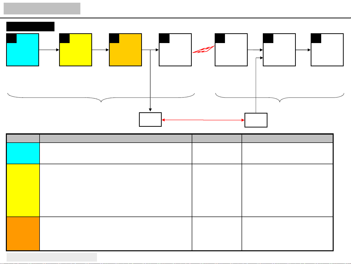
Trouble shooting
WIRELESS LH95
WIRELESS MODEL
a b c d e f g
INPUT MAIN IC
Analog
Digital
AV
Component
HDMI
OSD OSD
Wireless
RX MODULE
SB9111 +
SB9121 +
SIL9134
HDMI
LGE3159
LVDS
DTC30LM36 +
SIL9134
SIGNAL
CONVERTER
HDMI
TX MODULE
SIL9125 +
SB9120 +
SB9110
MAIN IC
LGE3369 +
LGE7329
LVDS
RGB
MEDIA-BOX
Service
only
HDMI JACK
Defect block Symptoms Wireless connection Check
a Bad (noise) image / No image
-osdis good
Bad sound / No sound
Wired
HDMI CABLE
No effect directly
HDMI5
HDMI JACK
▶ Check the EDID of HDMI & RGB
▶ Check cable & contact error
TV SET
LCD
MODULE
LGD V4
b Bad image
- IC’s cold soldering or memory defect accompanied noise on osd
Bad sound / No sound
Wireless connecting osd is displayed continually
- There is no video signal from Rx module to TV main ic, so TV
understand this time like disconnection state and display connecting
osd continually. And then, if TV is not activated rightly within 15min,
it will go to st-by mode.
C Bad image / Bad or No sound
Wireless connecting osd is displayed continually
-No image
*Focused on Wireless connecti on
No effect directly
No effect directly
No connection
No effect directly
No connection
▶ Check main ic basic power & power
sequence
▶ Control line check (I2C & etc)
▶ Check input/output video & audio
signal
▶ Check power & control line
▶ Check input/output signal
▶ Check inner HDMI cable connection
status
(There can be cable’s defect.)
Page 64
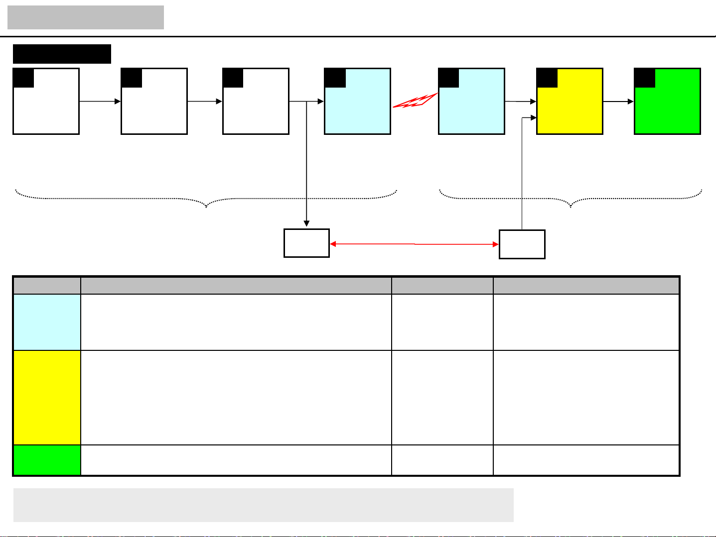
Trouble shooting
WIRELESS LH95
WIRELESS MODEL
a b c d e f g
INPUT MAIN IC
Analog
Digital
AV
Component
HDMI
OSD OSD
Wireless
RX MODULE
SB9111 +
SB9121 +
SIL9134
HDMI
LGE3159
LVDS
DTC30LM36 +
SIL9134
SIGNAL
CONVERTER
HDMI
TX MODULE
SIL9125 +
SB9120 +
SB9110
MAIN IC
LGE3369 +
LGE7329
LVDS
RGB
MEDIA-BOX
Service
only
HDMI JACK
Defect block Symptoms Wireless connection Check
d
e
Wireless connection osd is displayed continually
- That osd can be appeared by HDMI cable or Jack defect even
though wireless connection is completed.
(only Rx module)
Wired
HDMI CABLE
No connection
connection
HDMI5
HDMI JACK
▶ Check Wireless connecting osd
▶ Check inner HDMI cable connection
status
(There can be cable’s defect.)
TV SET
LCD
MODULE
LGD V4
F Bad image / No image
- IC’s cold soldering or memory defect accompanied noise on osd
Bad sound / No sound
g Bad image or No image No effect directly ▶ Ticon b/d or Inverter check
*Defect block means from itself to ahead of next part.
*Wireless TV is similar with the model usi n g LGE3 15 9 o r LGE3 36 9 e xce pt fo r w ire les s pa r ts.
No effect directly ▶ Check main ic basic power & power
sequence
▶ Check control line (I2C & etc)
▶ Check input/output video & audio
signal
▶ Check LVDS cable & wafer locking
(There can be cable’s defect.)
▶ Check power
Page 65
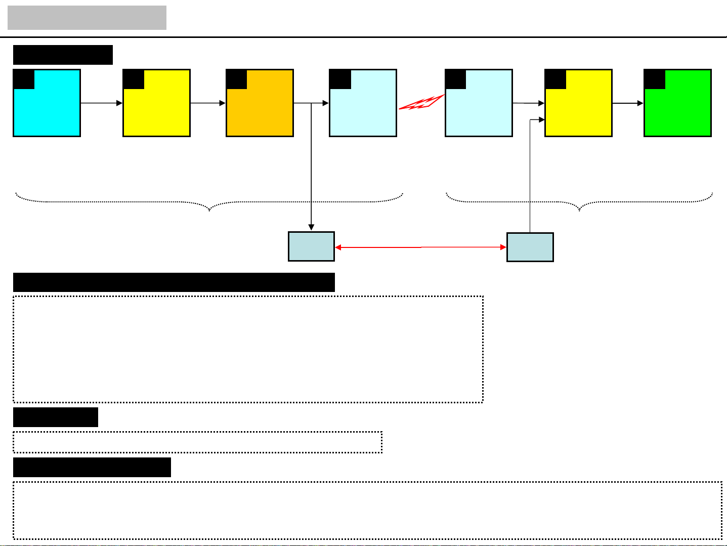
Trouble shooting
WIRELESS LH95
WIRELESS MODEL
a b c d e f g
INPUT MAIN IC
Analog
Digital
AV
Component
HDMI
OSD OSD
Wireless
RX MODULE
SB9111 +
SB9121 +
SIL9134
HDMI
LGE3159
LVDS
DTC30LM36 +
SIL9134
SIGNAL
CONVERTER
HDMI
TX MODULE
SIL9125 +
SB9120 +
SB9110
MAIN IC
LGE3369 +
LGE7329
LVDS
RGB
MEDIA-BOX
Service
only
HDMI JACK
Wired
HDMI CABLE
HDMI5
HDMI JACK
TV SET
※ Check first when Wireless connection is disable!
- Pairing
- S/W version check
- Fan defect
▷ TV Rx module fan defect: Check Fan error of TV In-start menu
▷ Media-Box fan defect: Check the red led’s blinking of Media-Box front
- Wireless interference check
▷ Refer to the installation method guide
- Inner HDMI cable’s connection status (From Rx/Tx module to Main)
LCD
MODULE
LGD V4
※ Check Tip
- In some cases, TV only or Wired mode make easy to check.
※ Caution & Information
- TV set & Media-Box is just 1:1 connection. (No multiple device connection)
- In order to download TV set, you must change the mode to HDMI5 or turn off Media-Box.
- Rx/Tx module’s performance is very sensitive to temperature. So, When you repair the defect, should keep up with
the original assembly state.
Page 66
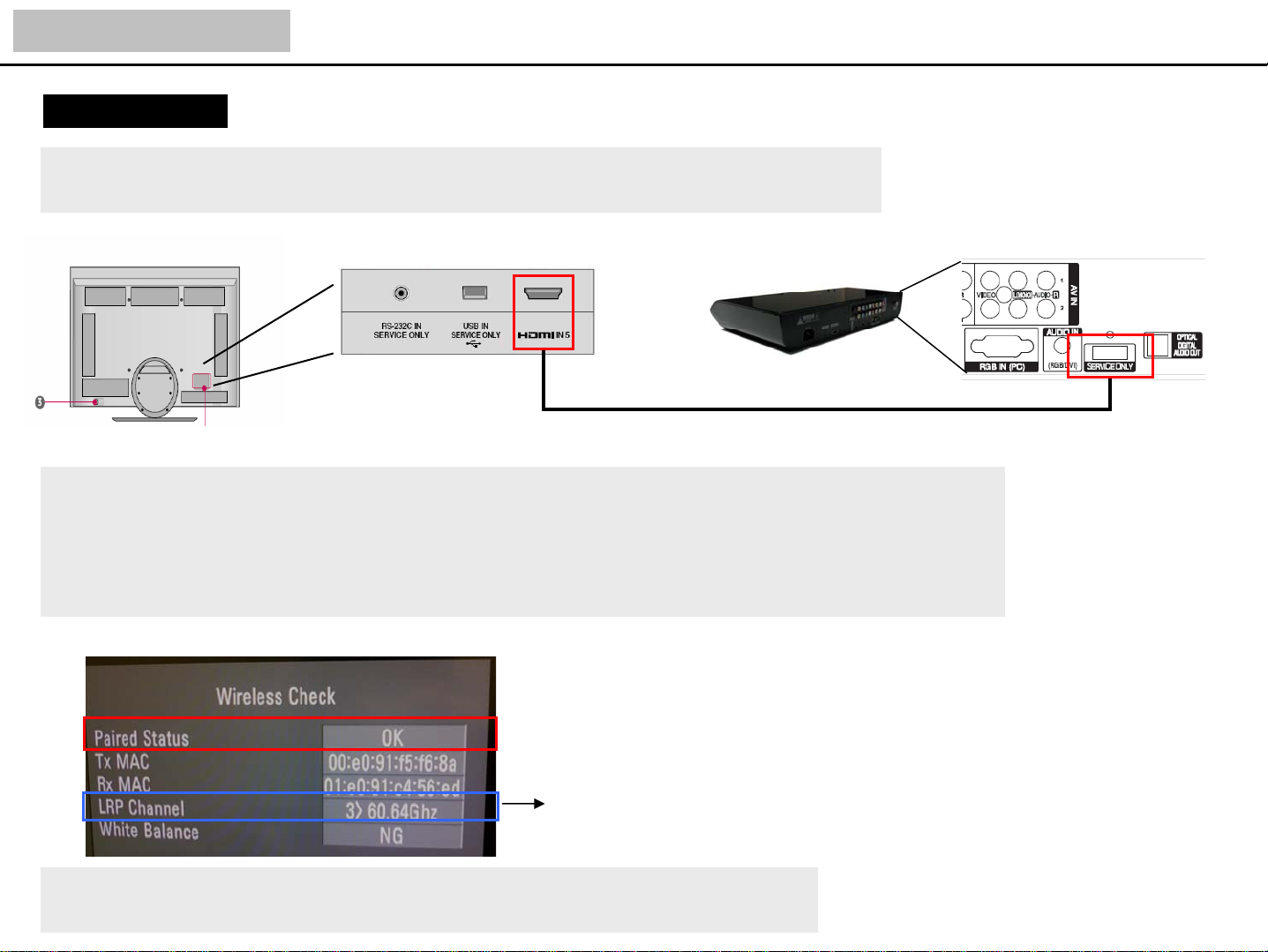
Trouble shooting
Pairing for SVC
1. Turn on the TV SET & Media-Box
2. Connect TV HDMI5 Jack & Media-Box rear [Service only] Jack with HDMI cable
HDMI CABLE
3. Enter the [IN START(Media Box)] menu and go to sub-title [9.Wireless check]
Enter menu and Push the left or right remote-controller button.
WIRELESS LH95
Check the Paired Status if changed from NG to OK
※ If s/w version of Tx/Rx module & TV/Media-box main isn’t matched, Wireless can’t be
connected, So at that time check the version and upgrade by usb
If there are 2 or more wireless tv set, it’s need to be set
channel respectively. (Must separate them more than 10m)
4. Remove HDMI cable & check wireless connection.
If connection is not completed, power off and on the TV & Media-Box.
Page 67
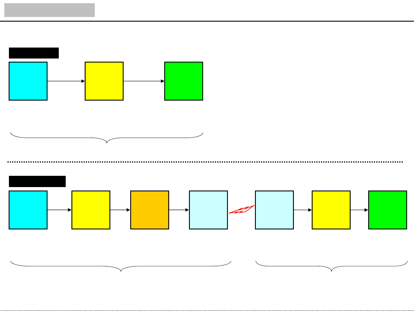
About Wireless TV
NORMAL MODEL
WIRELESS LH95
INPUT MAIN IC
AV
Component
Analog
Digital
MSTAR
BCM
HDMI
RGB
WIRELESS MODEL
INPUT MAIN IC
AV
Analog
Digital
LGE3159
Component
HDMI
RGB
TV SET
LVDS
LVDS
SIGNAL
CONVERTER
DTC30LM36 +
SIL9134
LGD
AUO
CMO
HDMI
LCD
MODULE
SIL9125 +
SB9120 +
SB9110
TX MODULE
Wireless
RX MODULE
SB9111 +
SB9121 +
SIL9134
HDMI
MAIN IC
LGE3369 +
LGE7329
LVDS
LCD
MODULE
LGD V4
MEDIA-BOX
TV SET
Page 68
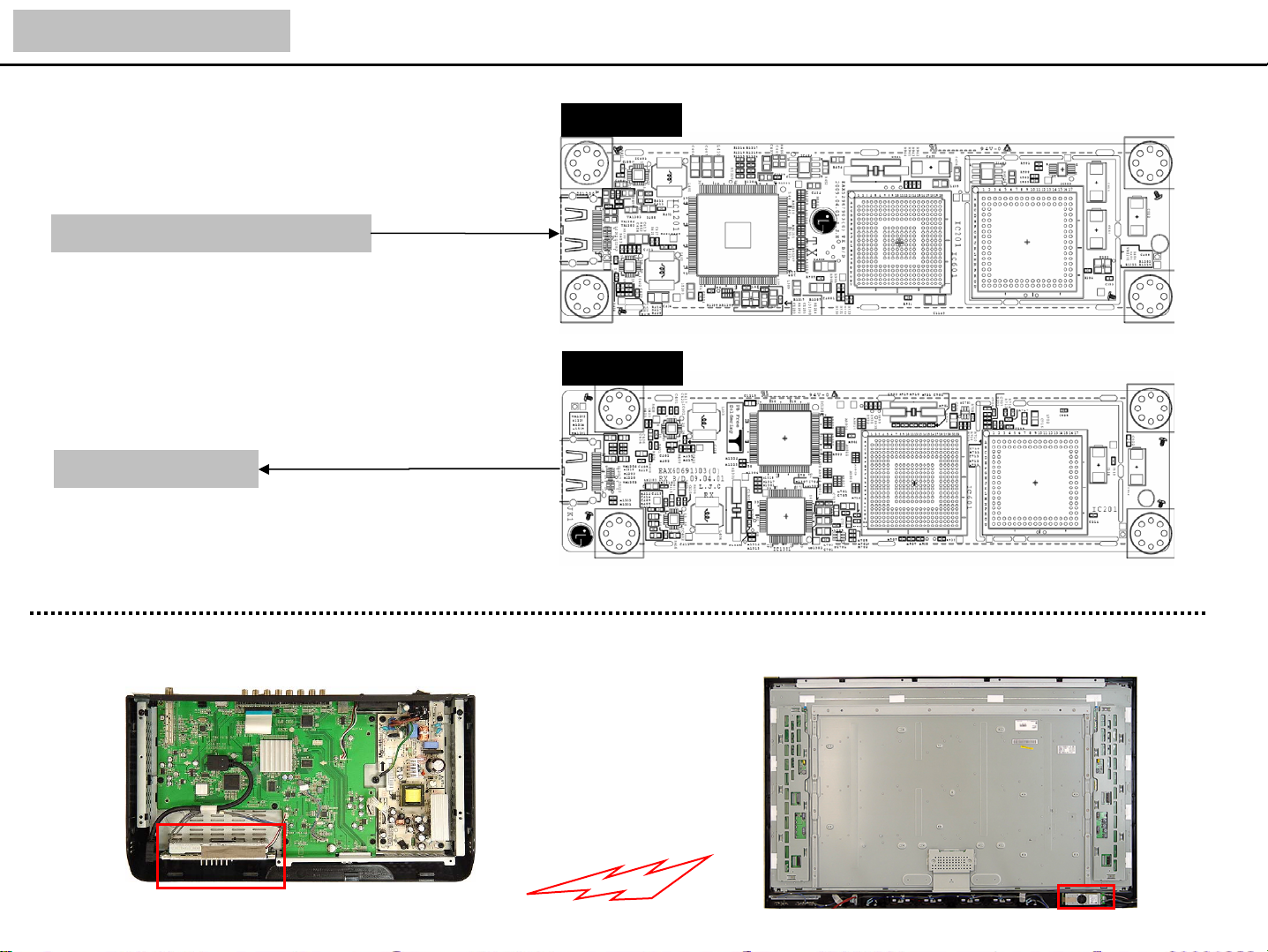
About Wireless TV
WIRELESS LH95
TX Module
From Media-Box Main b/d
To TV Main b/d
Media-Box
HDMI Cable
HDMI Cable
RX Module
SIL9125
SIL9134
PIC32MX
[MICOM]
SB9120
[B/B]
SB9121
[B/B]
TV SET
SB9110
[RF]
SB9111
[RF]
TX module
RX module
Page 69
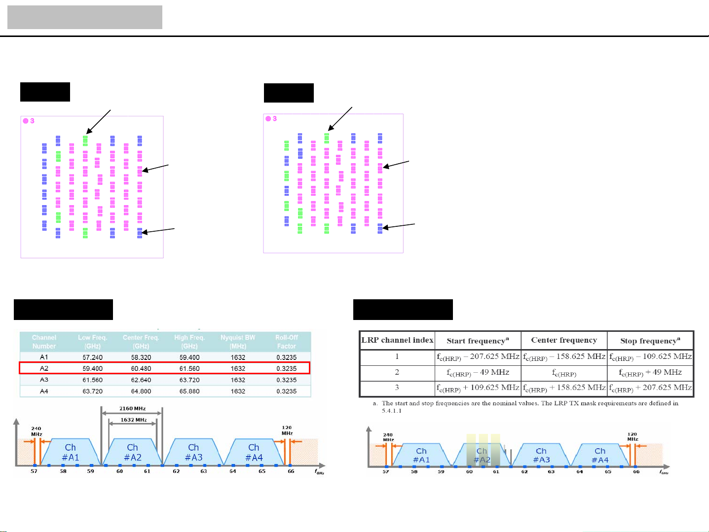
About Wireless TV
Top view of RF IC (Antenna)
WIRELESS LH95
SB9110
HRP Channel
LR
HR
Unused
SB9111
LR
HR
Unused
LRP Channel
F
c(HRP)
= 60.48㎓
Page 70
About Wireless TV
WIRELESS LH95
Wireless
LRP
TX module RX module
HRP
LRP: Control data
HRP: Video & Audio data
Wireless TV is similar to the walkie-talkie. We mu st m atch the cha nn el of Tx & Rx module.
There are 4 HRP channel(A1~A4). We use only A2 channel and 3 LRP channel like this [60 .32㎓],
[60.48㎓],[60.64㎓].
First thing, the LRP channel setting has to be matched in wired mode. There are not only channel
but also mac address that Tx/Rx modules have it’ s own for prev e nting wir ele ss int erf er ence .
Set the LRP channel and share the mac address each other, that’s called pairing.
After pairing, Antenna search and set the wireless path by LRP and then send video & audio data to
HRP channel.
Page 71
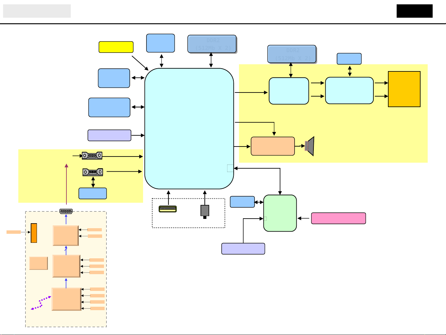
Block Diagram TV SET
NOT FOR USER
Connect to Rx b/d
HDMI CABLE
5.0V
8p wafer
JK505
HDMI
Transmitter
[SiI9134]
24
IC103
NAND-Flash
X100
X-tal(12㎒)
JK300
IC300
EEPROM
3.3V_L
1.8V_L
IC104
KIA7427F
IC102
S-Flash
(32Mb)
(512Mb)
For wireless
For wired
& 범용
IC101
NVRAM
24C512
R
e
s
e
t
IC200,201
(512Mb X 2)
(512Mb X 2)
IC100
LGE3159GV
Saturn5
DDR2
DDR2
MCLK
IC400
IC800,801
DDR2
DDR2
(512Mb X 2)
(512Mb X 2)
IC701
LGE7329A
Ursa
IC901
24C32
IC900
LG5110
Local dimming
MODULE
NTP3100L
I2S
(D-AMP)
HDMI_3
HDMI_2
IC1000
JK500JK504
24C16
IC1002
WT61P8
USB
Micom
IR & Local KEY
RS-232
Only for service
X1000
X-tal(24㎒)
MICOM
[PIC32]
Network
Processor
[SB9121]
RF
Transceiver
[SB9111]
Wireless RX Module
3.3V_L
2.5V_L
1.0V_L
2.5V_L
1.5V_L
1.2V_L
1.0V_L
Page 72
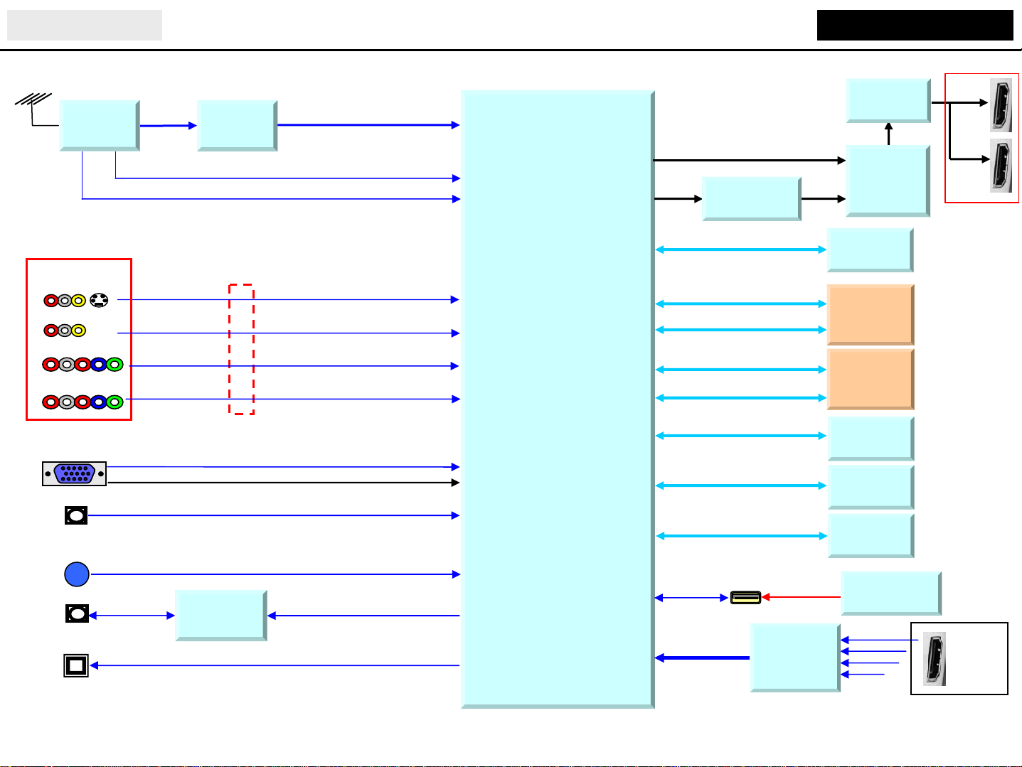
MEDIA-BOX(SIMPLE)Block Diagram
Can Tuner
(TDFR-Z751D)
Rear jack b’d
AV1
AV2
COMPONENT1
COMPONENT2
RGB
SPDIF
Demodulator
IF
(LG3900)
31P Wafer : rear jack
b’d & main b’d
(P1200)
RS-232C
(MAX3232CDR)
FE_TS_SERIAL
FE_VMAIN
FE_SIF
AV1_CVBS_IN
AV2_CVBS_IN
COMP1_Y/Pb/Pr
COMP2_Y/Pb/Pr
DSUB_ R/G/B
DSUB_H/VSYNC
AUDIO IN
IR (For test)
DGB_TX/RX
SPDIF_OUT
MSTAR
SATURN6
[MSD3369GV]
I2S
LVDS
USB_DM/DP
LVDS Receiver
(THC63LVD1024
/ DTC30LM36)
SPI_CK/CS/D0/D1
ADDR_D[0:15]
ADDR_A[0:12]
BDDR_D[0:15]
BDDR_A[0:12]
I2C
PCM_A[0:7]
I2C
TMDS[0:7]
HDMI_CEC
HPD
5V_HDMI
USB
TTL
USB Power
HDMI
4:1 Switch
(TDA9996)
HDMI Splitter
(PI3HDMI1210)
HDMI
Transmitter
(SiI9134)
Serial Flash
For Boot
DDR2 SDRAM
(1Gbit)
HYNIX/ELPIDA
DDR2 SDRAM
(512Mbit)
HYNIX/ELPIDA
MICOM
Weltrend
NAND Flash
HYNIX
(64MB)
EEPROM
AT24C512
MIC2009YM6-TR
USB Power
To TV
For
wireless
HDMI
Out
HDMI
1/2/3/4
Rear : 3
Front :1
HDMI
In
Page 73
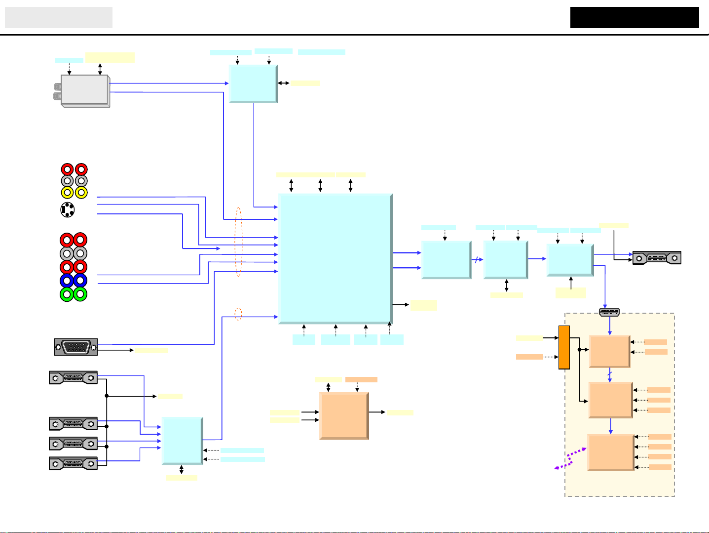
Block Diagram MEDIA-BOX(VIDEO)
ANT/
CABLE
IN
Composite
Video
IN
Component
(Y,Pb,Pr)
IN
RGB
IN
HDMI
IN
(x4)
5.0V_TU
Analog/D
TMB
Half-NIM
TUNER
FRONT
BACK
I2C_CH2(Demod
repeater
DDC_RGB
AV1_Y/C_IN
CEC_RX
HDMI
Switch
(4-to-1)
[TDA9996]
I2C_CH2
+3.3V_DTMB
DTMB/DVB-C
IF
Demodulator
ANALOG
VIDEO
INPUT
FE_VMAIN
AV1_CVBS_IN
AV2_CVBS_IN
COMP1-Y/Pb/Pr
COMP2-Y/Pb/Pr
DSUB-R/G/B
HDMI
DIGITAL
VIDEO
INPUT
D3.3V_HDMI
D1.8V_HDMI
+1.2V_DTMB
[LG3900]
TS
+3.3VA_DTMB
I2C_CH2
I2C_CH1
I2C_CH2
I2C_CH4
LCD/PDP
DIGITAL TV
PROCESSOR
[MSD3369GV]
D1.26V
D1.8V_DDR3.3V_V
_VDDC
I2C_CH4
CEC_RX
DDC_RGB
MiCOM
[WT61P8S]
DDP
D3.3V_L
D3.3V_
1
CEC_TX
DUAL
LVDS
D3.3V_2
Receiver
[DTC30LM36]
HDMI
TX_SEL
LVDS
D3.3V_2
30
Transmitter
[SiI9134]
D1.8V_1
HDMI
I2C_CH2
HDMI
I2C_CH4
D5.0V_W
D3.3V_3 D5.0V_1
HDMI
DeMUX
[PI3HDMI1210]
HDMI
TX_SEL
WiHD TX I/F
Wireless Module
CEC_TX
HDMI
Receiver
[SiI9125]
24
Network
Processor
[SB9120]
RF
Transceiver
[SB9110]
HDMI
OUT
3.3V_L
1.8V_L
3.3V_L
2.5V_L
1.0V_L
2.5V_L
1.5V_L
1.2V_L
1.0V_L
Page 74
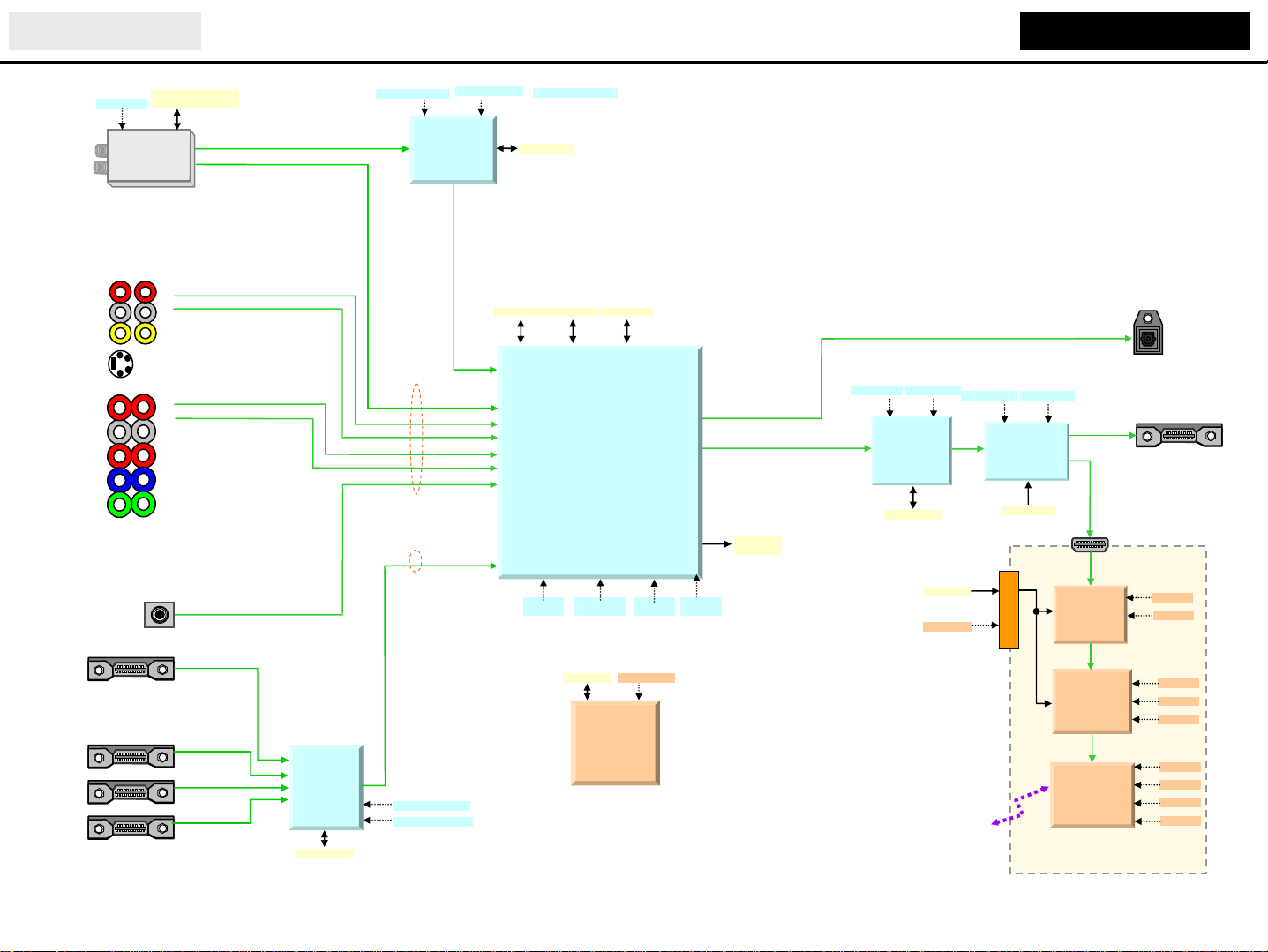
MEDIA-BOX(AUDIO)Block Diagram
ANT/
CABLE
IN
Composite
Video
IN
Component
(Y,Pb,Pr)
IN
RGB
IN
5.0V_TU
Analog/D
TMB
Half-NIM
TUNER
I2C_CH2(Demod
repeater
+3.3V_DTMB
DTMB/DVB-C
IF
Demodulator
ANALOG
AUDIO
INPUT
FE_SIF
A/V Audio-1
A/V Audio-2
COMP Audio-1
COMP Audio-2
RGB Audio
HDMI
DIGITAL
AUDIO
INPUT
+1.2V_DTMB
[LG3900]
TS
+3.3VA_DTMB
I2C_CH2
I2C_CH1
I2C_CH2
I2C_CH4
LCD/PDP
DIGITAL TV
PROCESSOR
[MSD3369GV]
D1.26V
D1.8V_DDR3.3V_V
_VDDC
DDP
D3.3V_
1
S/PDIF
I2S
HDMI
TX_SEL
D3.3V_2
Transmitter
[SiI9134]
D1.8V_1
HDMI
I2C_CH2
HDMI
I2C_CH4
D5.0V_W
D3.3V_3 D5.0V_1
HDMI
DeMUX
[PI3HDMI1210]
TX_SEL
WiHD TX I/F
HDMI
Receiver
[SiI9125]
S/PDIF
OUT
HDMI
OUT
3.3V_L
1.8V_L
HDMI
IN
(x4)
FRONT
BACK
HDMI
Switch
(4-to-1)
[TDA9996]
I2C_CH2
D3.3V_HDMI
D1.8V_HDMI
I2C_CH4
MiCOM
[WT61P8S]
D3.3V_L
Network
Processor
[SB9120]
RF
Transceiver
[SB9110]
Wireless Module
3.3V_L
2.5V_L
1.0V_L
2.5V_L
1.5V_L
1.2V_L
1.0V_L
Page 75
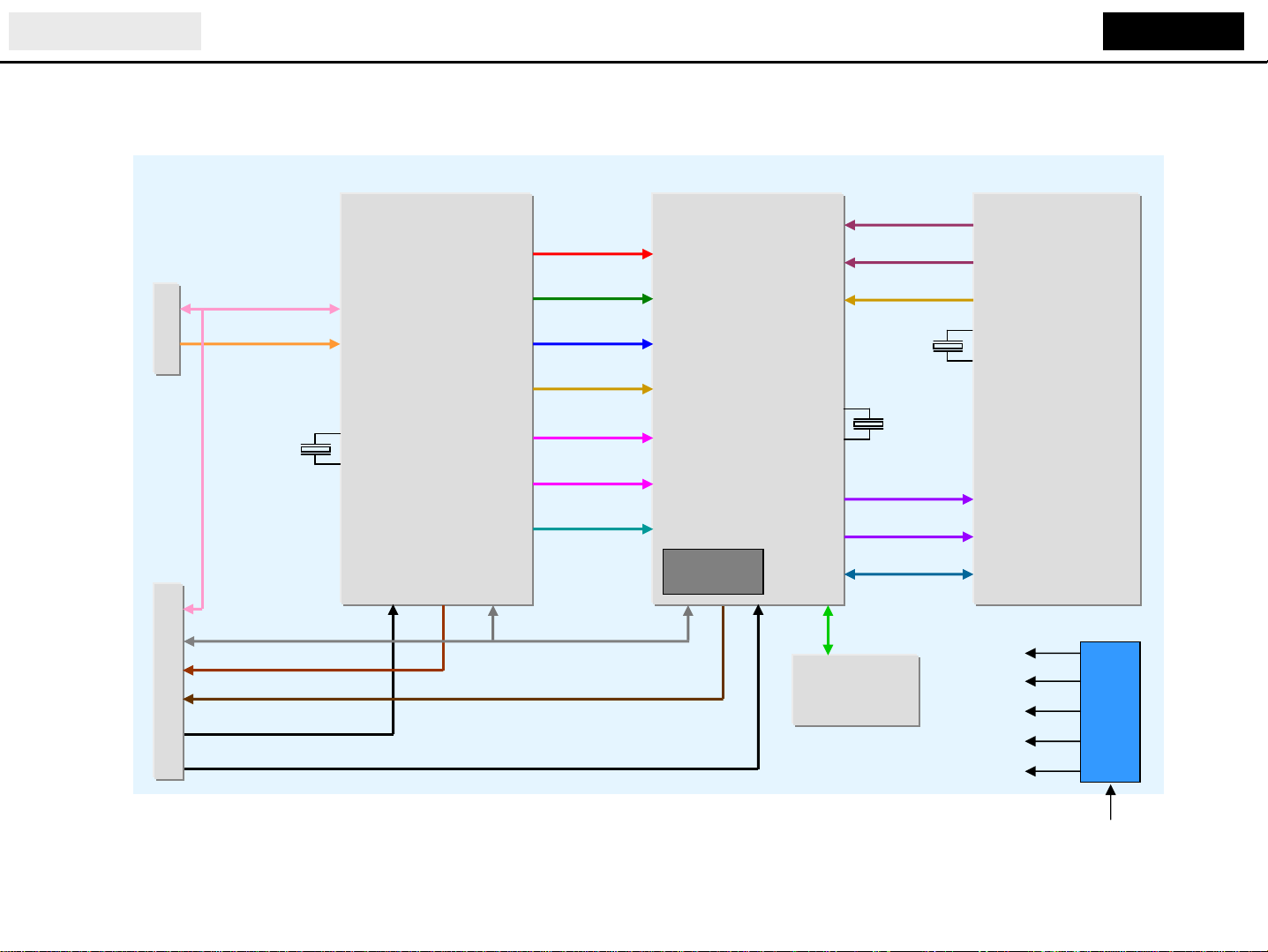
ADCI_P/N
TX MODULEBlock Diagram
HDMI
CABLE
Control
&
Power
CABLE
(12p)
DDC(2line)
TMDS(8line)
XTAL
(28.322MHz)
HDMI_INT
HDMI_RST#
SiI9125
HDMI
Receiver
D[35:0]
H/VSYNC
DE
IDCK
MCLK/SCK/W
S
I2S
SPDIFI
I2C(2line)
SiBEAM_INT
SiBEAM_RST#
SB9120
Network
Processor
Embedded
CPU
ADCQ_P/N
PCLK_P/N
OSC
(54MHz)
SLEEP
XTAL
(3.6864MHz)
DACI_P/
N
DACQ_P/N
RF Control
SPI Bus(4line)
MX1605
Serial Flash
SB9110
Transceiver
3.3V
2.5V
1.5V
1.2V
1.0V
RF
Power
Power Source
(5V)
Page 76
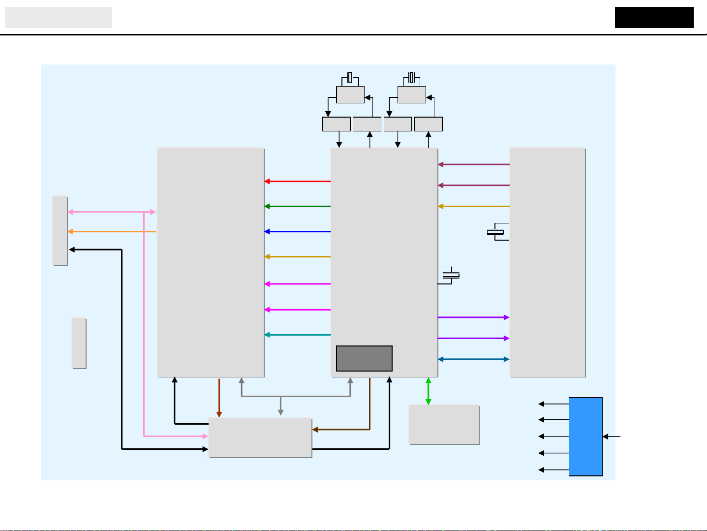
RX MODULEBlock Diagram
HDMI
CABLE
Power
CABLE
(8p)
DDC(2line)
TMDS(8line)
SiI9134
HDMI
Transceiver
XTAL
(27MHz)
D[35:0]
H/VSYNC
DE
IDCK
MCLK/SCK/W
S
I2S(4line)
SPDIFO
VCXO VCXO
Video
PLL
Video
DAC
Audio
SB9121
Network
Processor
Embedded
CPU
PLL
XTAL
(27MHz)
Audio
DAC
I2CI2C ACLKVCLK
ADCI_P/N
ADCQ_P/N
PCLK_P/N
(3.6864MHz)
DACI_P/N
DACQ_P/N
RF Control
OSC
(54MHz)
SLEEP
XTAL
SB9111
RF
Receiver
I2C(2line)
RST#
I2C(2line)
INT
Micom
(PIC32MX340F256H)
INT
RST#
SPI Bus
MX1605
Serial Flash
3.3V
2.5V
1.5V
1.2V
1.0V
Power
Power
Source
(5V)
 Loading...