

LG 55LE5400UC Schematic
LCD TV
SERVICE MANUAL
CAUTION
BEFORE SERVICING THE CHASSIS,
READ THE SAFETY PRECAUTIONS IN THIS MANUAL.
CHASSIS : LA02D
MODEL : 55LE5400
55LE5400-UC
North/Latin America http://aic.lgservice.com
Europe/Africa http://eic.lgservice.com
Asia/Oceania http://biz.lgservice.com
Internal Use Only
Printed in KoreaP/NO : MFL63283409 (1001-REV00)

LGE Internal Use OnlyCopyright LG Electronics. Inc. All right reserved.
Only for training and service purposes
- 2 -
CONTENTS
CONTENTS .............................................................................................. 2
SAFETY PRECAUTIONS ......................................................................... 3
SPECIFICATION....................................................................................... 6
ADJUSTMENT INSTRUCTION .............................................................. 10
EXPLODED VIEW .................................................................................. 17
SVC. SHEET ...............................................................................................
LGE Internal Use OnlyCopyright LG Electronics. Inc. All right reserved.
Only for training and service purposes
- 3 -
SAFETY PRECAUTIONS
Many electrical and mechanical parts in this chassis have special safety-related characteristics. These parts are identified by in the
Schematic Diagram and Exploded View.
It is essential that these special safety parts should be replaced with the same components as recommended in this manual to prevent
Shock, Fire, or other Hazards.
Do not modify the original design without permission of manufacturer.
General Guidance
An isolation Transformer should always be used during the
servicing of a receiver whose chassis is not isolated from the AC
power line. Use a transformer of adequate power rating as this
protects the technician from accidents resulting in personal injury
from electrical shocks.
It will also protect the receiver and it's components from being
damaged by accidental shorts of the circuitry that may be
inadvertently introduced during the service operation.
If any fuse (or Fusible Resistor) in this TV receiver is blown,
replace it with the specified.
When replacing a high wattage resistor (Oxide Metal Film Resistor,
over 1W), keep the resistor 10mm away from PCB.
Keep wires away from high voltage or high temperature parts.
Before returning the receiver to the customer,
always perform an AC leakage current check on the exposed
metallic parts of the cabinet, such as antennas, terminals, etc., to
be sure the set is safe to operate without damage of electrical
shock.
Leakage Current Cold Check(Antenna Cold Check)
With the instrument AC plug removed from AC source, connect an
electrical jumper across the two AC plug prongs. Place the AC
switch in the on position, connect one lead of ohm-meter to the AC
plug prongs tied together and touch other ohm-meter lead in turn to
each exposed metallic parts such as antenna terminals, phone
jacks, etc.
If the exposed metallic part has a return path to the chassis, the
measured resistance should be between 1MΩ and 5.2MΩ.
When the exposed metal has no return path to the chassis the
reading must be infinite.
An other abnormality exists that must be corrected before the
receiver is returned to the customer.
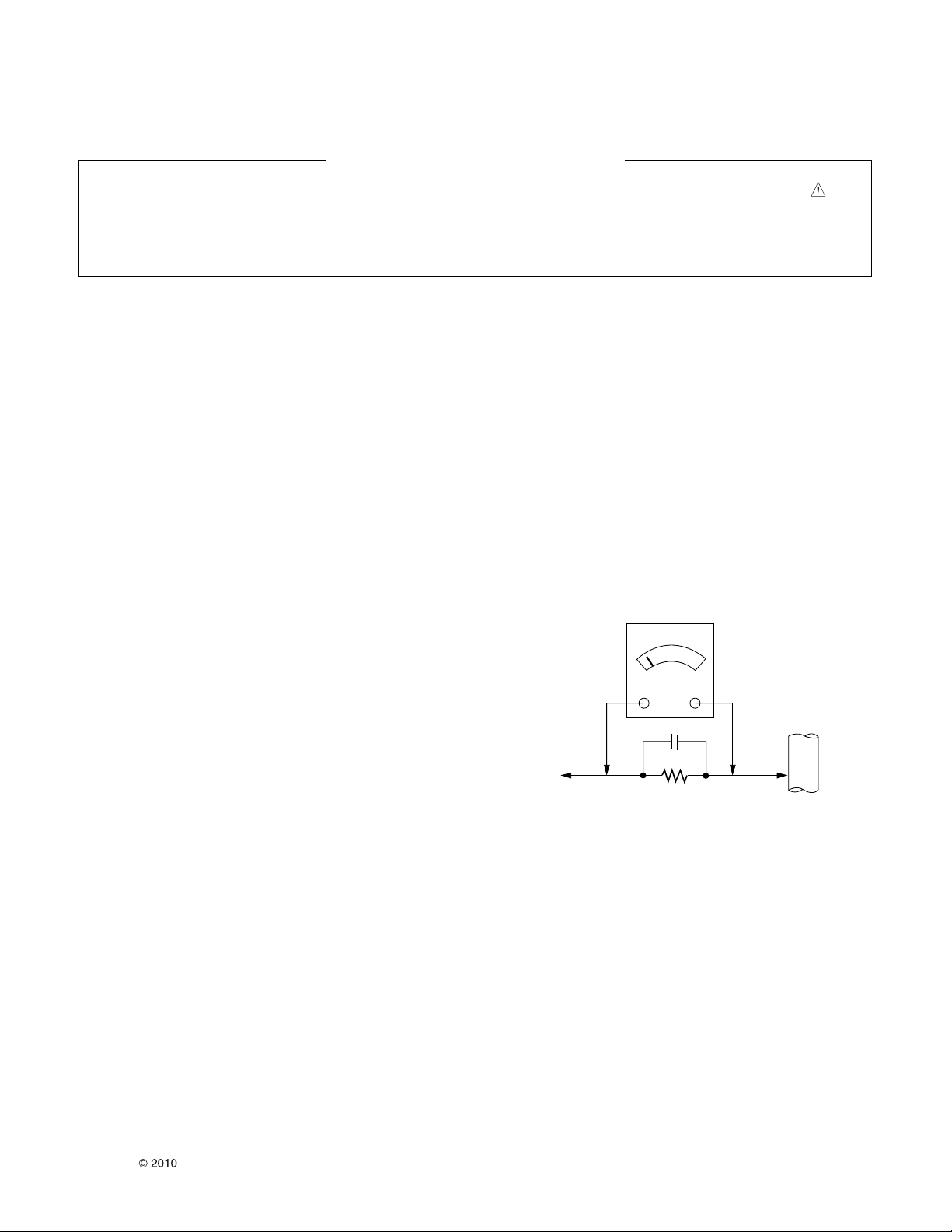
Leakage Current Hot Check (See below Figure)
Plug the AC cord directly into the AC outlet.
Do not use a line Isolation Transformer during this check.
Connect 1.5K/10watt resistor in parallel with a 0.15uF capacitor
between a known good earth ground (Water Pipe, Conduit, etc.)
and the exposed metallic parts.
Measure the AC voltage across the resistor using AC voltmeter
with 1000 ohms/volt or more sensitivity.
Reverse plug the AC cord into the AC outlet and repeat AC voltage
measurements for each exposed metallic part. Any voltage
measured must not exceed 0.75 volt RMS which is corresponds to
0.5mA.
In case any measurement is out of the limits specified, there is
possibility of shock hazard and the set must be checked and
repaired before it is returned to the customer.
Leakage Current Hot Check circuit
1.5 Kohm/10W
To Instrument’s
exposed
METALLIC PARTS
Good Earth Ground
such as WATER PIPE,
CONDUIT etc.
AC Volt-meter
IMPORTANT SAFETY NOTICE
0.15uF

LGE Internal Use OnlyCopyright LG Electronics. Inc. All right reserved.
Only for training and service purposes
- 4 -
CAUTION: Before servicing receivers covered by this service
manual and its supplements and addenda, read and follow the
SAFETY PRECAUTIONS on page 3 of this publication.
NOTE: If unforeseen circumstances create conflict between the
following servicing precautions and any of the safety precautions on
page 3 of this publication, always follow the safety precautions.
Remember: Safety First.
General Servicing Precautions
1. Always unplug the receiver AC power cord from the AC power
source before;
a. Removing or reinstalling any component, circuit board
module or any other receiver assembly.
b. Disconnecting or reconnecting any receiver electrical plug or
other electrical connection.
c. Connecting a test substitute in parallel with an electrolytic
capacitor in the receiver.
CAUTION: A wrong part substitution or incorrect polarity
installation of electrolytic capacitors may result in an
explosion hazard.
2. Test high voltage only by measuring it with an appropriate high
voltage meter or other voltage measuring device (DVM,
FETVOM, etc) equipped with a suitable high voltage probe.
Do not test high voltage by "drawing an arc".
3. Do not spray chemicals on or near this receiver or any of its
assemblies.
4. Unless specified otherwise in this service manual, clean
electrical contacts only by applying the following mixture to the
contacts with a pipe cleaner, cotton-tipped stick or comparable
non-abrasive applicator; 10% (by volume) Acetone and 90% (by
volume) isopropyl alcohol (90%-99% strength)
CAUTION: This is a flammable mixture.
Unless specified otherwise in this service manual, lubrication of
contacts in not required.
5. Do not defeat any plug/socket B+ voltage interlocks with which
receivers covered by this service manual might be equipped.
6. Do not apply AC power to this instrument and/or any of its
electrical assemblies unless all solid-state device heat sinks are
correctly installed.
7. Always connect the test receiver ground lead to the receiver
chassis ground before connecting the test receiver positive
lead.
Always remove the test receiver ground lead last.
8. Use with this receiver only the test fixtures specified in this
service manual.
CAUTION: Do not connect the test fixture ground strap to any
heat sink in this receiver.
Electrostatically Sensitive (ES) Devices
Some semiconductor (solid-state) devices can be damaged easily
by static electricity. Such components commonly are called
Electrostatically Sensitive (ES) Devices. Examples of typical ES
devices are integrated circuits and some field-effect transistors and
semiconductor "chip" components. The following techniques
should be used to help reduce the incidence of component
damage caused by static by static electricity.
1. Immediately before handling any semiconductor component or
semiconductor-equipped assembly, drain off any electrostatic
charge on your body by touching a known earth ground.
Alternatively, obtain and wear a commercially available
discharging wrist strap device, which should be removed to
prevent potential shock reasons prior to applying power to the
unit under test.
2. After removing an electrical assembly equipped with ES
devices, place the assembly on a conductive surface such as
aluminum foil, to prevent electrostatic charge buildup or
exposure of the assembly.
3. Use only a grounded-tip soldering iron to solder or unsolder ES
devices.
4. Use only an anti-static type solder removal device. Some solder
removal devices not classified as "anti-static" can generate
electrical charges sufficient to damage ES devices.
5. Do not use freon-propelled chemicals. These can generate
electrical charges sufficient to damage ES devices.
6. Do not remove a replacement ES device from its protective
package until immediately before you are ready to install it.
(Most replacement ES devices are packaged with leads
electrically shorted together by conductive foam, aluminum foil
or comparable conductive material).
7. Immediately before removing the protective material from the
leads of a replacement ES device, touch the protective material
to the chassis or circuit assembly into which the device will be
installed.
CAUTION: Be sure no power is applied to the chassis or circuit,
and observe all other safety precautions.
8. Minimize bodily motions when handling unpackaged
replacement ES devices. (Otherwise harmless motion such as
the brushing together of your clothes fabric or the lifting of your
foot from a carpeted floor can generate static electricity
sufficient to damage an ES device.)
General Soldering Guidelines
1. Use a grounded-tip, low-wattage soldering iron and appropriate
tip size and shape that will maintain tip temperature within the
range or 500°F to 600°F.
2. Use an appropriate gauge of RMA resin-core solder composed
of 60 parts tin/40 parts lead.
3. Keep the soldering iron tip clean and well tinned.
4. Thoroughly clean the surfaces to be soldered. Use a mall wirebristle (0.5 inch, or 1.25cm) brush with a metal handle.
Do not use freon-propelled spray-on cleaners.
5. Use the following unsoldering technique
a. Allow the soldering iron tip to reach normal temperature.
(500°F to 600°F)
b. Heat the component lead until the solder melts.
c. Quickly draw the melted solder with an anti-static, suction-
type solder removal device or with solder braid.
CAUTION: Work quickly to avoid overheating the circuit
board printed foil.
6. Use the following soldering technique.
a. Allow the soldering iron tip to reach a normal temperature
(500°F to 600°F)
b. First, hold the soldering iron tip and solder the strand against
the component lead until the solder melts.
c. Quickly move the soldering iron tip to the junction of the
component lead and the printed circuit foil, and hold it there
only until the solder flows onto and around both the
component lead and the foil.
CAUTION: Work quickly to avoid overheating the circuit
board printed foil.
d. Closely inspect the solder area and remove any excess or
splashed solder with a small wire-bristle brush.
SERVICING PRECAUTIONS

LGE Internal Use OnlyCopyright LG Electronics. Inc. All right reserved.
Only for training and service purposes
- 5 -
IC Remove/Replacement
Some chassis circuit boards have slotted holes (oblong) through
which the IC leads are inserted and then bent flat against the
circuit foil. When holes are the slotted type, the following technique
should be used to remove and replace the IC. When working with
boards using the familiar round hole, use the standard technique
as outlined in paragraphs 5 and 6 above.
Removal
1. Desolder and straighten each IC lead in one operation by gently
prying up on the lead with the soldering iron tip as the solder
melts.
2. Draw away the melted solder with an anti-static suction-type
solder removal device (or with solder braid) before removing the
IC.
Replacement
1. Carefully insert the replacement IC in the circuit board.
2. Carefully bend each IC lead against the circuit foil pad and
solder it.
3. Clean the soldered areas with a small wire-bristle brush.
(It is not necessary to reapply acrylic coating to the areas).
"Small-Signal" Discrete Transistor
Removal/Replacement
1. Remove the defective transistor by clipping its leads as close as
possible to the component body.
2. Bend into a "U" shape the end of each of three leads remaining
on the circuit board.
3. Bend into a "U" shape the replacement transistor leads.
4. Connect the replacement transistor leads to the corresponding
leads extending from the circuit board and crimp the "U" with
long nose pliers to insure metal to metal contact then solder
each connection.
Power Output, Transistor Device
Removal/Replacement
1. Heat and remove all solder from around the transistor leads.
2. Remove the heat sink mounting screw (if so equipped).
3. Carefully remove the transistor from the heat sink of the circuit
board.
4. Insert new transistor in the circuit board.
5. Solder each transistor lead, and clip off excess lead.
6. Replace heat sink.
Diode Removal/Replacement
1. Remove defective diode by clipping its leads as close as
possible to diode body.
2. Bend the two remaining leads perpendicular y to the circuit
board.
3. Observing diode polarity, wrap each lead of the new diode
around the corresponding lead on the circuit board.
4. Securely crimp each connection and solder it.
5. Inspect (on the circuit board copper side) the solder joints of
the two "original" leads. If they are not shiny, reheat them and if
necessary, apply additional solder.
Fuse and Conventional Resistor
Removal/Replacement
1. Clip each fuse or resistor lead at top of the circuit board hollow
stake.
2. Securely crimp the leads of replacement component around
notch at stake top.
3. Solder the connections.
CAUTION: Maintain original spacing between the replaced
component and adjacent components and the circuit board to
prevent excessive component temperatures.
Circuit Board Foil Repair
Excessive heat applied to the copper foil of any printed circuit
board will weaken the adhesive that bonds the foil to the circuit
board causing the foil to separate from or "lift-off" the board. The
following guidelines and procedures should be followed whenever
this condition is encountered.
At IC Connections
To repair a defective copper pattern at IC connections use the
following procedure to install a jumper wire on the copper pattern
side of the circuit board. (Use this technique only on IC
connections).
1. Carefully remove the damaged copper pattern with a sharp
knife. (Remove only as much copper as absolutely necessary).
2. carefully scratch away the solder resist and acrylic coating (if
used) from the end of the remaining copper pattern.
3. Bend a small "U" in one end of a small gauge jumper wire and
carefully crimp it around the IC pin. Solder the IC connection.
4. Route the jumper wire along the path of the out-away copper
pattern and let it overlap the previously scraped end of the good
copper pattern. Solder the overlapped area and clip off any
excess jumper wire.
At Other Connections
Use the following technique to repair the defective copper pattern
at connections other than IC Pins. This technique involves the
installation of a jumper wire on the component side of the circuit
board.
1. Remove the defective copper pattern with a sharp knife.
Remove at least 1/4 inch of copper, to ensure that a hazardous
condition will not exist if the jumper wire opens.
2. Trace along the copper pattern from both sides of the pattern
break and locate the nearest component that is directly
connected to the affected copper pattern.
3. Connect insulated 20-gauge jumper wire from the lead of the
nearest component on one side of the pattern break to the lead
of the nearest component on the other side.
Carefully crimp and solder the connections.
CAUTION: Be sure the insulated jumper wire is dressed so the
it does not touch components or sharp edges.
LGE Internal Use OnlyCopyright LG Electronics. Inc. All right reserved.
Only for training and service purposes
1. Application range
This spec sheet is applied LCD TV with LA02D/E chassis.
2. Requirement for Test
Each part is tested as below without special appointment.
1) Temperature: 25±5ºC, (77°±9ºF), CST: 40±5°C
2) Relative Humidity: 65±10%
3) Power Voltage : Standard input voltage(100-240V~, 50/60Hz)
* Standard Voltage of each product is marked by models
4) Specification and performance of each parts are followed
each drawing and specification by part number in
accordance with BOM.
5) The receiver must be operated for about 20 minutes prior to
the adjustment.
3. Test method
1) Performance: LGE TV test method followed
2) Demanded other specification
- Safety : UL, CSA, IEC specification
- EMC: FCC, ICES, IEC specification
- Wireless : WirelessHD Specification (Option)
Model Market Appliance
XXLE5500-UA North America Safety : UL1492, CSA C22.2.No.1,
XXLE7500-UC EMC : FCC Class B, IEC Class B
XXLE8500-UA Wireless HD: Option
- 6 -
SPECIFICATION
NOTE : Specifications and others are subject to change without notice for improvement.
4. General Specification(TV)
No Item Specification Remark
1 Receivable System 1) ATSC / NTSC-M
2 Available Channel VHF : 02 ~ 13
UHF : 14 ~ 69
DTV : 02 ~ 69
CATV : 01 ~ 135
CADTV : 01 ~ 135
3 Input Voltage 1) AC 100 ~ 240V 50/60Hz
4 Market North America
5 Screen Size Edge LED 42 inch Wide(1920x1080) FHD + 120Hz 42LE5500-UA/ 42LE7500-UC
47 inch Wide(1920x1080) FHD + 120Hz 47LE5500-UA/ 47LE7500-UC
55 inch Wide(1920x1080) FHD + 120Hz 55LE5500-UA/ 55LE7500-UC
IOP LED 47 inch Wide(1920x1080)
FHD+TM240Hz
47LE8500-UA
55 inch Wide(1920x1080)
FHD+TM240Hz
55LE8500-UA
6 Aspect Ratio 16:9
7 Tuning System FS
8 LCD Module Edge LED
LC420EUH-SCA1 (Slim Edge Led)
LGD 42LE5500-UA/42LE7500-UC
LC470EUH-SCA1 (Slim Edge Led)
LGD 47LE5500-UA/47LE7500-UC
LC550EUB-SCA1 (Slim Edge Led)
LGD 55LE5500-UA/ 55LE7500-UC
IOP LED
0MUK-SCA1 (LCD Panel)
LGD 47LE8500-UA
LUTHS470EALZD (Back Light Assy)
Heesung
LC550MUK-SCA1 (LCD Panel) LGD 55LE8500-UA
LC55030011A (Back Light Assy)
Razen
9 Operating Environment Temp : 0 ~ 40 deg
Humidity : ~ 80 %
10 Storage Environment Temp : -20 ~ 60 deg
Humidity : -85 %

- 7 -
LGE Internal Use OnlyCopyright LG Electronics. Inc. All right reserved.
Only for training and service purposes
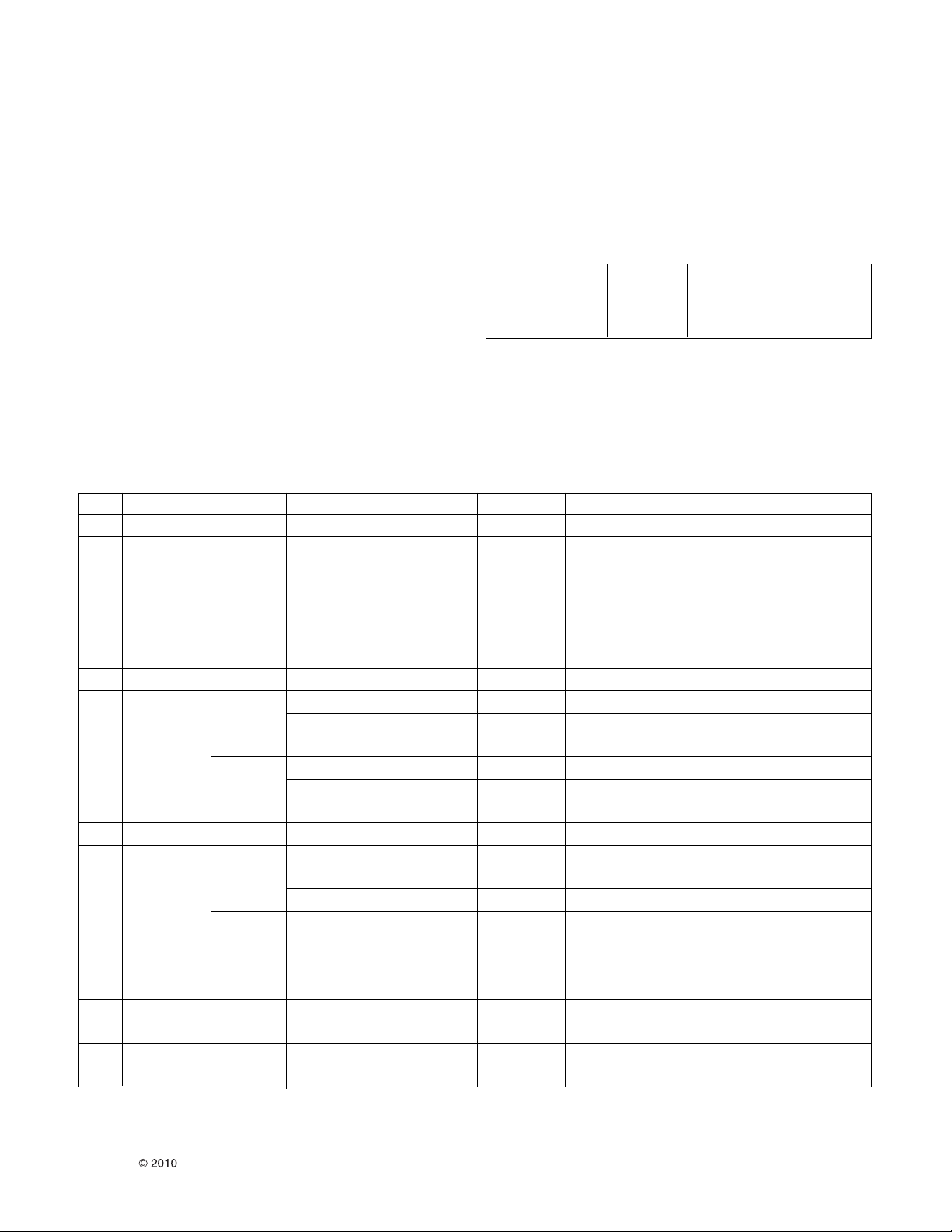
5. Chrominance & Luminance
5.1. 55LE5500-UA/55LE7500-UC/55LE5400-UC
No. Item Min Typ Max Unit Remarks
1 Max Luminance
360 450
cd/m
2
(Center 1-point / Full White Pattern)
2 Luminance uniformity 1.3 5point
3 Color coordinate RED X Typ. 0.649 Typ.
(Default) Y -0.03 0.332 +0.03
GREEN X 0.307
Y 0.595
BLUE X 0.149
Y 0.059
WHITE X 0.279
Y 0.292
4 Contrast ratio Module 1000:1 1400:1
DCR 4,500,000:1 5,000,000:1
6 Color Temperature Cool 0.267 0.269 0.271
13000K
The W/B Tolerance is
0.271 0.273 0.275 ±0.015 for picture quality by
Medium 0.283 0.285 0.287
9300K
DQA.
0.291 0.293 0.295
Warm 0.311 0.313 0.315
6500K
0.327 0.329 0.331
- 8 -
LGE Internal Use OnlyCopyright LG Electronics. Inc. All right reserved.
Only for training and service purposes
6. Component Video Input (Y, CB/PB, CR/PR)
No Resolution H-freq(kHz) V-freq.(kHz) Pixel clock Proposed
1. 720*480 15.73 60 13.5135 SDTV ,DVD 480I
2. 720*480 15.73 59.94 13.5 SDTV ,DVD 480I
3. 720*480 31.50 60 27.027 SDTV
4. 720*480 31.47 59.94 27.0 SDTV
5. 1280*720 45.00 60.00 74.25 HDTV
6. 1280*720 44.96 59.94 74.176 HDTV
7. 1920*1080 33.75 60.00 74.25 HDTV
8. 1920*1080 33.72 59.94 74.176 HDTV
9. 1920*1080 67.500 60 148.50 HDTV
10. 1920*1080 67.432 59.94 148.352 HDTV
11. 1920*1080 27.000 24.000 74.25 HDTV
12. 1920*1080 26.97 23.976 74.176 HDTV
13. 1920*1080 33.75 30.000 74.25 HDTV
14. 1920*1080 33.71 29.97 74.176 HDTV
7. RGB Input (PC)
No Resolution H-freq(kHz) V-freq.(kHz) Pixel clock Proposed
PC DDC
1. 640*350 31.468 70.09 25.17 EGA X
2. 720*400 31.469 70.08 28.32 DOS O
3. 640*480 31.469 59.94 25.17 VESA(VGA) O
4 . 800*600 37.879 60.31 40.00 VESA(SVGA) O
5. 1024*768 48.363 60.00 65.00 VESA(XGA) O
6. 1280*768 47.776 59.87 79.50 CVT(WXGA) X
7. 1360*768 47.712 60.015 85.50 VESA(WXGA) X
8. 1280*1024 63.981 60.020 108.00 VESA(SXGA) O
9. 1920*1080 66.587 59.934 148.5 HDTV 1080P O
LGE Internal Use OnlyCopyright LG Electronics. Inc. All right reserved.
Only for training and service purposes
- 9 -
8. HDMI input (PC/DTV)
No Resolution H-freq(kHz) V-freq.(kHz) Pixel clock Proposed
PC DDC
1. 640*350 31.468 70.09 25.17 EGA X
2. 720*400 31.469 70.08 28.32 DOS O
3. 640*480 31.469 59.94 25.17 VESA(VGA) O
4 . 800*600 37.879 60.31 40.00 VESA(SVGA) O
5. 1024*768 48.363 60.00 65.00 VESA(XGA) O
6. 1280*768 47.776 59.870 79.50 CVT(WXGA) X
7. 1360*768 47.712 60.015 85.50 VESA(WXGA) X
8. 1280*1024 63.981 60.020 108.00 VESA(SXGA) O
9. 1920*1080 67.5 60 148.5 HDTV 1080P O
DTV
1 720*480 31.5 60 27.027 SDTV 480P
2 720*480 31.47 59.94 27.00 SDTV 480P
3 1280*720 45.00 60.00 74.25 HDTV 720P
4 1280*720 44.96 59.94 74.176 HDTV 720P
5 1920*1080 33.75 60.00 74.25 HDTV 1080I
6 1920*1080 33.72 59.94 74.176 HDTV 1080I
7 1920*1080 67.500 60 148.50 HDTV 1080P
8 1920*1080 67.432 59.939 148.352 HDTV 1080P
9 1920*1080 27.000 24.000 74.25 HDTV 1080P
10 1920*1080 26.97 23.976 74.176 HDTV 1080P
11 1920*1080 33.75 30.000 74.25 HDTV 1080P
12 1920*1080 33.71 29.97 74.176 HDTV 1080P
LGE Internal Use OnlyCopyright LG Electronics. Inc. All right reserved.
Only for training and service purposes
- 10 -
ADJUSTMENT INSTRUCTION
1. Application range
This spec sheet is applied to LA02D & LA02E Chassis applied
LCD TV all models manufactured in TV factory
2. Specification
2.1 Because this is not a hot chassis, it is not necessary
to use an isolation transformer. However, the use of
isolation transformer will help protect test instrument.
2.2 Adjustment must be done in the correct order.
2.3 The adjustment must be performed in the
circumstance of 25±5°C of temperature and 65±10%
of relative humidity
2.4 The input voltage of the receiver must keep
100~240V, 50/60Hz.
2.5 The receiver must be operated for about 5 minutes
prior to the adjustment when module is in the
circumstance of over 15. In case of keeping module
is in the circumstance of 0°C, it should be placed in
the circumstance of above 15°C for 2 hours In case
of keeping module is in the circumstance of below 20°C, it should be placed in the circumstance of
above 15°C for 3 hours.
Caution) When still image is displayed for a period of 20
minutes or longer (especially where W/B scale is
strong. Digital pattern 13ch and/or Cross hatch
pattern 09ch), there can some afterimage in the
black level area.
3. Adjustment items
3.1. Main PCBA check process
• ADC adjustment: Component 480i, 1080p / RGB-PC 1080p
• EDID downloads for HDMI and RGB-PC
Remark) Above adjustment items can be also performed in
Final Assembly if needed. Adjustment items in
both PCBA and final assembly stages can be
checked by using the INSTART Menu
1.ADJUST CHECK.
3.2 Final assembly adjustment
•White Balance adjustment
•RS-232C functionality check
•Factory Option setting per destination
•Ship-out mode setting (In-Stop)
•GND and HI-POT test
3.3 Appendix
• Tool option menu, USB Download (S/W Update, Option and
Service only)
• Manual adjustment for ADC calibration and White balance.
• Shipment conditions, Channel pre-set
4. MAIN PCBA Adjustments
4.1. ADC Calibration
(1) Overview
ADC adjustment is needed to find the optimum black level
and gain in Analog-to-Digital device and to compensate
RGB deviation.
(2) Equipment & Condition
1) Jig (RS-232C protocol)
2) MSPG-925 Series Pattern Generator(MSPG-925FA)
- Resolution : 480i Comp1 (MSPG-925FA: model-209,
pattern-65)
- Resolution : 1080p Comp1 (MSPG-925FA: model-225,
pattern-65)
- Resolution : 1080p RGB (MSPG-925FA: model-225,
pattern-65)
- Pattern: Horizontal 100% Color Bar Pattern
- Pattern level: 0.7±0.1 Vp-p
- Image
(3) Adjustment
1) Adjustment method
- Using RS-232, adjust items listed in 3.1 in the other
shown in “4.1.3.3”
2) Adj. protocol
Ref.) ADC Adj. RS232C Protocol_Ver1.0
3) Adj. order
• aa 00 00 [Enter ADC adj. mode]
• xb 00 40 [Change input source to Component1(No
action)]
• ad 00 10 [Adjust 480i Comp1]
• ad 00 10 [Adjust 1080p Comp1]
• xb 00 60 [Change input source to RGB(No action)]
• ad 00 10 [Adjust 1080p RGB]
• ad 00 90 End adj.

- 11 -
LGE Internal Use OnlyCopyright LG Electronics. Inc. All right reserved.
Only for training and service purposes
4.2 MAC Address and ESN Key Write
4.2.1 Equipment & Condition
• Play file: Serial.exe
• MAC Address edit
• Input Start / End MAC address
4.2.2 Download method
4.2.2.1 Communication Prot connection
Connect: PCBA Jig-> RS-232C Port== PC-> RS-232C Port
4.2.2.2 MAC Address Download
• Com 1,2,3,4 and 115200(Baudrate)
• Port connection button click(1)
• Load button click(2) for MAC Address write.
• Start MAC Address write button(3)
• Check the OK Or NG
4.2.2.3 Input the ESN Key
• download Model sending Key file
• input by 1 by SET so as not to be duplicated
4.3 LAN PORT + ESN INSPECTION (Automatic IP)
4.3.1 Equipment & Condition
• Each other connection to LAN Port of IP Hub and Jig
4.3.2 LAN inspection solution
• LAN Port connection with PCB
• Network setting at MENU Mode of TV
• setting automatic IP
• Setting state confirmation
- If automatic setting is finished, you confirm IP and MAC
Address.
4.3.3 ESN Key confirmation
• confirm Key input Data at ESN MENU Mode
PCBA
PC(RS-232C)
RS-232C Port

- 12 -
LGE Internal Use OnlyCopyright LG Electronics. Inc. All right reserved.
Only for training and service purposes
4.4 LAN PORT INSPECTION(PING TEST)
4.4.1. Equipment setting
1) Play the LAN Port Test PROGRAM.
2) Input IP set up for an inspection to Test
Program.
*IP Number : 12.12.2.2
4.4.2. LAN PORT inspection (PING TEST)
1) Play the LAN Port Test Program.
2) connect each other LAN Port Jack.
3) Play Test (F9) button and confirm OK Message.
4) remove LAN CABLE

- 13 -
LGE Internal Use OnlyCopyright LG Electronics. Inc. All right reserved.
Only for training and service purposes
4.5 EDID/DDC Download
(1) Overview
It is a VESA regulation. A PC or a MNT will display an
optimal resolution through information sharing without any
necessity of user input. It is a realization of “Plug and Play”.
(2) Equipment
• Since embedded EDID data is used, EDID download JIG,
HDMI cable and D-sub cable are not need.
• Adjust by using remote controller.
(3) Download method
1) Press Adj. key on the Adj. R/C,
2) Select EDID D/L menu.
3) By pressing Enter key, EDID download will begin
4) If Download is successful, OK is display, but If
Download is failure, NG is displayed.
5) If Download is failure, Re-try downloads.
Caution) When EDID Download, must remove RGB/HDMI
Cable.
(4) EDID DATA

- 14 -
LGE Internal Use OnlyCopyright LG Electronics. Inc. All right reserved.
Only for training and service purposes
5. Final Assembly Adjustment
5.1. White Balance Adjustment
(1) Overview
• W/B adj. Objective & How-it-works
- Objective: To reduce each Panel’s W/B deviation
- How-it-works: When R/G/B gain in the OSD is at 192, it
means the panel is at its Full Dynamic
Range. In order to prevent saturation of
Full Dynamic range and data, one of
R/G/B is fixed at 192, and the other two is
lowered to find the desired value.
- Adj. condition : normal temperature
1) Surrounding Temperature: 25±5ºC
2) Warm-up time: About 5 Min
3) Surrounding Humidity: 20% ~ 80%
(2) Adj. condition and cautionary items
• Lighting condition in surrounding area surrounding lighting
should be lower 10 lux. Try to isolate adj. area into dark
surrounding.
• Probe location: Color Analyzer (CA-210) probe should be
within 10cm and perpendicular of the module surface
(80°~ 100°)
• Aging time
1) After Aging Start, Keep the Power ON status during
5 Minutes.
2) In case of LCD, Back-light on should be checked
using no signal or Full-white pattern.
(3) Equipment
1) Color Analyzer: CA-210 (NCG: CH 9 / WCG: CH12 /
LED : CH14)
2) Adj. Computer (During auto adj., RS-232C protocol is
needed)
3) Adjust Remocon
4) Video Signal Generator MSPG-925F 720p/216-Gray
(Model:217, Pattern:78)
-> Only when internal pattern is not available
• Color Analyzer Matrix should be calibrated using CS-1000
(4) Equipment connection
(5) Adj. Command (Protocol)
1) RS-232C Command used during auto-adj.
2) Adjustment Map
(6) Adj. method
• Auto adj. method
1) Set TV in adj. mode using POWER ON key
2) Zero calibrate probe then place it on the center of the
Display
3) Connect Cable(RS-232C)
4) Select mode in adj. Program and begin adj.
5) When adj. is complete (OK Sing), check adj. status pre
mode (Warm, Medium, Cool)
6) Remove probe and RS-232C cable to complete adj.
(7) Reference (White Balance Adj. coordinate and color
temperature)
• Luminance: 216 Gray
• Standard color coordinate and temperature using CS1000
• Standard color coordinate and temperature using CA-210
(CH 14)
Colo r Analyzer
Comp ut er
Pattern Ge n e r ator
RS-232C
RS-232C
RS-232C
Probe
Signal Source
* If TV internal pattern is used, not needed
Connection Diagram of Automatic Adjustment
Mode Color Coordination Temp ∆UV
xy
COOL 0.269 0.273 13000K 0.0000
MEDIUM 0.285 0.293 9300K 0.0000
WARM 0.313 0.329 6500K 0.0000
Mode Color Coordination Temp ∆UV
xy
COOL 0.269±0.002 0.273±0.002 13000K 0.0000
MEDIUM 0.285±0.002 0.293±0.002 9300K 0.0000
WARM 0.313+0.002 0.329±0.002 6500K 0.0000
- 15 -
LGE Internal Use OnlyCopyright LG Electronics. Inc. All right reserved.
Only for training and service purposes
• Standard color coordinate and temperature using CA210(CH 14) – by aging time
1) Edge/IOP LED models
5.2. Tool Option setting & Inspection per
countries
(1) Overview
• Tool option selection is only done for models in Non-USA
North America due to rating
• Applied model: LA02D and LA02E Chassis applied to
CANADA and MEXICO
(2) Country Group selection
• Press ADJ key on the Adj. R/C, and then select Country
Group Menu
• Depending on destination, select KR or US, then on the
lower Country option, select US, CA, MX. Selection is
done using +, - KEY
(3) Tool Option Inspection
• Press Adj. key on the Adj. R/C, and then check Tool
option.
5.3. Local dimming inspection (Optional)
5.3.1. Edge LED models with local dimming
(1) Press ‘TILT” key of the Adj. R/C and check moving
patterns. The black bar patterns moves from left to right.
If local dimming function does not work, a whole screen
shows full white.
5.3.2. IOP LED models with local dimming
(1) Press ‘TILT” key of the Adj. R/C and check moving
patterns. The black cross-bar patterns moves from top-left to
Bottom-right. If local dimming function does not work, a whole
screen shows full white.
5.4. Ship-out mode check (In-stop)
• After final inspection, press In-Stop key of the Adj. R/C and
check that the unit goes to Stand-by mode.

- 16 -
LGE Internal Use OnlyCopyright LG Electronics. Inc. All right reserved.
Only for training and service purposes
6. GND and Hi-pot Test
6.1. Method
6.1.1. GND & HI-POT auto-check preparation
(1) Check the POWER CABLE and SIGNAL CABE
insertion condition
6.1.2. GND & HI-POT auto-check
(1) Pallet moves in the station. (POWER CORD / AV
CORD is tightly inserted)
(2) Connect the AV JACK Tester.
(3) Controller (GWS103-4) on.
(4) GND Test (Auto)
- If Test is failed, Buzzer operates.
- If Test is passed, execute next process (Hi-pot test).
(Remove A/V CORD from A/V JACK BOX)
(5) HI-POT test (Auto)
- If Test is failed, Buzzer operates.
- If Test is passed, GOOD Lamp on and move to next
process automatically.
6.2. Checkpoint
• TEST voltage
- GND: 1.5KV/min at 100mA
- SIGNAL: 3KV/min at 100mA
• TEST time: 1 second
• TEST POINT
- GND TEST = POWER CORD GND & SIGNAL CABLE
METAL GND
- Internal Pressure TEST = POWER CORD GND & LIVE &
NEUTRAL
• LEAKAGE CURRENT: At 0.5mArms

- 17 -
LGE Internal Use OnlyCopyright LG Electronics. Inc. All right reserved.
Only for training and service purposes
1. Tool option menu
APPENDIX
- 18 -
LGE Internal Use OnlyCopyright LG Electronics. Inc. All right reserved.
Only for training and service purposes
2. USB S/W Download (option)
(1) Put the USB Stick to the USB socket
(2) Automatically detecting update file in USB Stick
- If your downloaded program version in USB Stick is Low, it didn’t work.
But your downloaded version is High, USB data is automatically detecting
(3) Show the message “Copying files from memory”
(4) Updating is staring.
(5) Updating Completed, The TV will restart automatically
(6) If your TV is turned on, check your updated version and Tool option. (explain the Tool option, next stage)
* If downloading version is more high than your TV have, TV can lost all channel data. In this case, you have to channel recover.
if all channel data is cleared, you didn’t have a DTV/ATV test on production line.
* After downloading, have to adjust TOOL OPTION again.
1) Push "IN-START" key in service remote controller.
2) Select "Tool Option 1" and Push “OK” button.
3) Punch in the number. (Each model has their number

- 19 -
LGE Internal Use OnlyCopyright LG Electronics. Inc. All right reserved.
Only for training and service purposes
5. Optional adjustments (Optional)
5.1. Manual ADC Calibration
5.1.1. Equipment & Condition
(1) Adjustment Remocon
(2) 801GF (802B, 802F, 802R) or MSPG925FA Pattern Generator
- Resolution: 480i Comp1 (MSPG-925FA: model-209, pattern-65)
- Resolution: 1080p Comp1 (MSPG-925FA: model-225, pattern-65)
- Resolution : 1080p RGB (MSPG-925FA: model-225, pattern-65)
- Pattern : Horizontal 100% Color Bar Pattern
- Pattern level: 0.7±0.1 Vp-p
5.1.2 Adjust method
5.1.3.1 ADC 480i/1080p Comp1, RGB
(1) Check connected condition of Comp1/RGB cable to the equipment
(2) Give a 480i Mode, Horizontal 100% Color Bar Pattern to Comp1. (MSPG-925FA ->Model: 209, Pattern: 65)
(3) Change input mode as Component1 and picture mode as “Standard”
(4) Press the In-start Key on the ADJ remote after at least 1 min of signal reception. Then, select 7.External ADC.
And Press OK or Right Button for going to sub menu.
(5) Press OK in Comp 480i menu
(6) Give a 1080p Mode, Horizontal 100% Color Bar Pattern to Comp1. (MSPG-925FA Model: 225, Pattern: 65)
(7) Press OK in Comp 1080p menu
(8) Perform (6) and (7) in RGB-PC
(9) If ADC Comp is successful, “ADC Component Success” is displayed.
If ADC calibration is failure, “ADC Component Fail” is displayed.
(10) If ADC calibration is failure, after rechecking ADC pattern or condition, retry calibration
(11) If ADC RGB calibration is successful, “ADC RGB Success” is displayed.
If ADC calibration is failure, “ADC RGB Fail” is displayed.
(12) If ADC calibration is failure, after recheck ADC pattern or condition, retry calibration
5.2. Manual White balance Adjustment
5.2.1. Adj. condition and cautionary items
(1) Lighting condition in surrounding area surrounding lighting should be lower 10 lux. Try to isolate adj. area into dark
surrounding.
(2) Probe location: Color Analyzer (CA-210) probe should be within 10cm and perpendicular of the module surface (80°~ 100°)
(3) Aging time
1) After Aging Start, Keep the Power ON status during 5 Minutes.
2) In case of LCD, Back-light on should be checked using no signal or Full-white pattern.
5.2.2. Equipment
(1) Color Analyzer: CA-210 (NCG: CH 9 / WCG: CH12 / LED: CH14)
(2) Adj. Computer (During auto adj., RS-232C protocol is needed)
(3) Adjust Remocon
(4) Video Signal Generator MSPG-925F 720p/216-Gray (Model: 217, Pattern: 78)
5.2.3. Adjustment
(1) Set TV in Adj. mode using POWER ON
(2) Zero Calibrate the probe of Color Analyzer, then place it on the center of LCD module within 10cm of the surface.
(3) Press ADJ key EZ adjust using adj. R/C 6. White-Balance then press the cursor to the right (KEY
G ).
When KEY(
G ) is pressed 216 Gray internal pattern will be displayed.
(4) One of R Gain / G Gain / B Gain should be fixed at 192, and the rest will be lowered to meet the desired value.
(5) Adj. is performed in COOL, MEDIUM, WARM 3 modes of color temperature.
• If internal pattern is not available, use RF input. In EZ Adj. menu 6.White Balance, you can select one of 2 Test-pattern:
ON, OFF. Default is inner(ON). By selecting OFF, you can adjust using RF signal in 216 Gray pattern.

- 20 -
LGE Internal Use OnlyCopyright LG Electronics. Inc. All right reserved.
Only for training and service purposes
5.3. V-COM Adjustment
(1) Press the ADJ key of Adjustment remote controller. EZ ADJUST mode.
(2) Select the “13.V-Com”.
(3) At the V-Com adjustment Mode use
FGKey and adjust V-Com voltage. (Refer to Picture)
- After finding minimum point of Flicker save data using
A (OK) Key.
(4) Exit
5.4. Speaker output check
5.4.1. Audio input condition
(1) RF input: Mono, 1KHz sine wave signal, 100% Modulation
(2) CVBS, Component: 1KHz sine wave signal (0.4Vrms)
(3) RGB PC: 1KHz sine wave signal (0.7Vrms)
5.4.2. Specification
500
300
EXPLODED VIEW
IMPORTANT SAFETY NOTICE
Many electrical and mechanical parts in this chassis have special safety-related characteristics. These
parts are identified by in the Schematic Diagram and EXPLODED VIEW.
It is esse ntia l that t hese speci al safety parts shoul d be repla ced with the same compo nent s as
recommended in this manual to prevent X-RADIATION, Shock, Fire, or other Hazards.
Do not modify the original design without permission of manufacturer.
200
120
840
800
810
530
850
540
830
880
800
400
910
920
900
Only for training and service purposes
- 21 -
LGE Internal Use OnlyCopyright LG Electronics. Inc. All right reserved.

COMPONENT/AV
REAR JACK
REAR AV
COMPONENT2
COMPONENT1
REAR AV
COMPONENT2
COMPONENT1
JK100
PPJ237-01
DEV
[RD1]E-LUG
6C
[RD1]O-SPRING
5C
[RD1]CONTACT
4C
[WH1]O-SPRING
5B
[YL1]CONTACT
4A
[YL1]O-SPRING
5A
[YL1]E-LUG
6A
[RD2]E-LUG
6H
[RD2]O-SPRING_2
5H
[RD2]CONTACT
4H
[WH2]O-SPRING
5G
[RD2]O-SPRING_1
5F
[RD2]E-LUG-S
7F
[BL2]O-SPRING
5E
[BL2]E-LUG-S
7E
[GN2]CONTACT
4D
[GN2]O-SPRING
5D
[GN2]E-LUG
6D
[RD3]E-LUG
6N
[RD3]O-SPRING_2
5N
[RD3]CONTACT
4N
[WH3]O-SPRING
5M
[RD3]O-SPRING_1
5L
[RD3]E-LUG-S
7L
[BL3]O-SPRING
5K
[BL3]E-LUG-S
7K
[GN3]CONTACT
4J
[GN3]O-SPRING
5J
[GN3]E-LUG
6J
D104
5.6V
D105
5.6V
D106
5.6V
D107
5.5V
D3.3V
R108
2.7K
C105
100pF
50V
C104 1uF
25V
R104
470K
C101 1uF
R103
470K
25V
R113
1K
R110
0
R109
0
R105
0
C109
100pF
50V
C108
100pF
50V
C106
47pF
50V
AV
REAR_AV_DET
9:G3
REAR_AV_R_IN
10:B5
REAR_AV_L_IN
10:B5
REAR_AV_CVBS
11:C4
D108
5.6V
D109
5.6V
D110
5.5V
D111
5.5V
D112
5.5V
D114
5.6V
D119
5.6V
D115
5.6V
D116
5.5V
D117
5.5V
D113
5.6V
D3.3V
R114
470K
R115
470K
R116
2.7K
C114
27pF
50V
C112
27pF
50V
C113
27pF
50V
R124
470K
R123
470K
C127
27pF
50V
C128
27pF
50V
C115
100pF
50V
C116
1uF
25V
C117
1uF
25V
L102
270nH
L100
270nH
L101
270nH
D3.3V
C132
1uF
25V
C131
1uF
25V
L103
270nH
L104
270nH
R117
0
R118
0
R125
2.7K
C130
100pF
50V
R127
0
R126
0
C122
27pF
50V
C120
27pF
50V
C121
27pF
50V
C133
27pF
50V
C134
27pF
50V
COMPONENT2
R119
1K
C123
100pF
C124
100pF
R100
0
R101
0
R102
10
COMPONENT1
R129
1K
C137
100pF
C136
100pF
R106
0
R107
0
COMP2_DET
9:G5
COMP2_R_IN
10:B5
COMP2_L_IN
10:B5
COMP2_Pr
11:D3
COMP2_Pb
11:D3
COMP2_Y
11:D3
COMP1_DET
9:G5
COMP1_R_IN
10:B5
COMP1_L_IN
10:B5
COMP1_Pr
11:D4
COMP1_Pb
11:D4
THE SYMBOL MARK OF THIS SCHEMETIC DIAGRAM INCORPORATES
SPECIAL FEATURES IMPORTANT FOR PROTECTION FROM X-RADIATION.
FILRE AND ELECTRICAL SHOCK HAZARDS, WHEN SERVICING IF IS
ESSENTIAL THAT ONLY MANUFATURES SPECFIED PARTS BE USED FOR
THE CRITICAL COMPONENTS IN THE SYMBOL MARK OF THE SCHEMETIC.
L105
D118
5.5V
C129
27pF
50V
270nH
GP2_BCM_ATSC
COMPONENT / AV REAR
C135
27pF
50V
R131
10
COMP1_Y
11:D4
09/10/xx
1 100
HDMI SWITCH 1.8V POWER
1.8V FOR HDMI SW
R202
+1.8V_HDMI
OPT
C201
10K
4.7uF
D1.8V
POWER_ON/OFF2_1
R200
120K
OPT
C200
4.7uF
10V
OPT
DEV
Q200
AO3438
EBK60752601
D
S
G
R201
0
Seperated from Common sheet83
N.America & Korea only use 1.8V control
THE SYMBOL MARK OF THIS SCHEMETIC DIAGRAM INCORPORATES
SPECIAL FEATURES IMPORTANT FOR PROTECTION FROM X-RADIATION.
FILRE AND ELECTRICAL SHOCK HAZARDS, WHEN SERVICING IF IS
ESSENTIAL THAT ONLY MANUFATURES SPECFIED PARTS BE USED FOR
THE CRITICAL COMPONENTS IN THE SYMBOL MARK OF THE SCHEMETIC.
HDMI_POWER
09/10/xxGP2_BCM_ATSC
2 100
EARPHONE BLOCK
USB BLOCK
EARPHONE AMP
HP/BT_LOUT_N
11:F2
HP/BT_LOUT_P
11:F2
HP/BT_ROUT_N
11:F2
HP/BT_ROUT_P
11:F2
R300
R301
4.7K
OPT
1uF
C307
1uF
10V
EARPHONE JACK SIDE
HP_L_OUT
Q26
HP_R_OUT
Q21
C304
1uF
10V
C305
10V
C306
1uF
10V
INL-
INL+
INR+
INR-
4.7K
R302
OPT
R303
Q300
MMBT3904-(F)
OPT
Q301
MMBT3904-(F)
OPT
Close to the IC
SGND
OUTL
15
16
1
2
3
4
EAN60724701
5
OUTR
C
B
E
C
B
E
+3.3V_NORMAL
L302
10uH
C308
1uF
10V
IC300
TPA6132A2
6G07G18
B
9:G3
SIDE_HP_DET
B
EN14VDD
13
HPVSS
E
C
E
C
C315
10uF
10V
12
11
10
C316
2.2uF
10V
C317
0.1uF
16V
HPVDD
CPP
PGND
CPN
9
Q303
MMBT3904-(F)
OPT
Q302
MMBT3904-(F)
OPT
C
B
C318
2.2uF
10V
C319
2.2uF
10V
R314
120
E
Q306
ISA1530AC1
OPT
+3.5V_ST
R315
150
OPT
2SC3052
Q307
R306
100K
OPT
R308
0
1/16W
R307
0
1/16W
Q308
2SC3052
L304
BG2012B080TF
C321
22000pF
50V
+3.3V_NORMAL
R309
4.7K
C
E
L303
BG2012B080TF
C320
22000pF
50V
USB2
+5V_USB
C311
C313
HP_L_OUT
OPT
R310
0
R311
1K
B
SIDE_HP_MUTE
HP_R_OUT
10:D4
0.1uF
USB_PWRFLT2
10uF
10V
R321
2.7K
+3.3V_NORMAL
R320
4.7K
OPT
USB_PWRON2
10:D4
10:D4
10:D4
USB_DM2
USB_DP2
IC301
AP2191SG-13
GND
1
IN_1
2
IN_2
3
EN
4
EAN60921001
DEV
R3180
NC
8
OUT_2
7
OUT_1
6
FLG
5
D303
CDS3C05HDMI1
5.6V
ESD_USB
L301
MLB-201209-0120P-N2
120-ohm
C310
100uF
16V
D301
CDS3C05HDMI1
5.6V
ESD_USB
P30 1
KJA -UB- 4-0 004
1234
USB DOW N S TREA M
5
USB
USB(DVR Ready)
EAG41945401
CHANGE USB_PWRFLT PULL-UP FROM 5V TO 3.3V
USB1 (DVR Ready)
+3.3V_NORMAL
IN_1
IN_2
GND
EN
AP2191SG-13
DEV
IC302
1
2
3
4
EAN60921001
CDS3C05HDMI1
NC
8
MLB-201209-0120P-N2
OUT_2
7
OUT_1
6
FLG
5
R3170
D302
5.6V
ESD_USB
L300
120-ohm
100uF
CDS3C05HDMI1
ESD_USB
C309
16V
D300
5.6V
P30 0
KJA -UB- 4-0 004
1234
USB DOW N S TREA M
5
EAG41945401
+5V_USB
C312
10:D4
C314
0.1uF
10uF
10V
USB_PWRFLT1
10:D4
10:D4
R322
2.7K
JK300
KJA-PH-0-0177
5GND
4L
3DETECT
DEV
1R
EAG61030001
C
B
OPT
E
SIDE_HP_MUTE
Q23;81:I4
USB_DM1
USB_DP1
R319
4.7K
OPT
USB_PWRON1
10:D4
WIRELESS I2C LEVEL SHIFTER
LEVEL SHIFTER
+3.3V_NORMAL
R324
10K
OPT
Q304
G
FDV301N
WIRELESS_SCL
WIRELESS_SDA
OPT
D
S
D
Q305
FDV301N
OPT
THE SYMBOL MARK OF THIS SCHEMETIC DIAGRAM INCORPORATES
SPECIAL FEATURES IMPORTANT FOR PROTECTION FROM X-RADIATION.
FILRE AND ELECTRICAL SHOCK HAZARDS, WHEN SERVICING IF IS
ESSENTIAL THAT ONLY MANUFATURES SPECFIED PARTS BE USED FOR
THE CRITICAL COMPONENTS IN THE SYMBOL MARK OF THE SCHEMETIC.
SCL3_3.3V
G
SDA3_3.3V
S
GP2_BCM_ATSC
USB/EAR-PHONE
09/10/xx
3 100
SIDE COMPONENT LINE
86:M25
86:M21
86:M22
SIDE_COMP_Y
SIDE_COMP_Pr
SIDE_COMP_Pb
82
R400
CLOSE TO MAIN IC
75
R401
75
R402
C400 0.1uF
C401 0.1uF
C402 0.1uF
SIDE_COMP-Y
SIDE_COMP-Pr
SIDE_COMP-Pb
11:C4;11:D4
11:C4;11:D4
11:C4;11:D4
THE SYMBOL MARK OF THIS SCHEMETIC DIAGRAM INCORPORATES
SPECIAL FEATURES IMPORTANT FOR PROTECTION FROM X-RADIATION.
FILRE AND ELECTRICAL SHOCK HAZARDS, WHEN SERVICING IF IS
ESSENTIAL THAT ONLY MANUFATURES SPECFIED PARTS BE USED FOR
THE CRITICAL COMPONENTS IN THE SYMBOL MARK OF THE SCHEMETIC.
SIDE GENDER LINE
09/10/xx
SIDE_GENDER_LINE 4 100
SMD GASKET FOR EMI (8*6*5.5 FOR LE5400/5500/7500)
SMD GASKET FOR EMI (8*6*12.5T)
GASKET on the Bottom
DEV
GAS 1
GAS 4
GAS 3
GAS 2
GAS 6
GAS 5
GAS 7
GAS 9
GAS 8
GAS 10
GAS 12
GAS 11
SMD GASKET FOR EMI (8*6*7.5 FOR LE8500)
GASKET on the Bottom
DEV
GAS 1-*1
GAS 4-*1
GAS 3-*1
GAS 2-*1
GAS 6-*1
GAS 5-*1
GAS 7-*1
GAS 9-*1
GAS 8-*1
GAS 10-* 1
GAS 12-* 1
GAS 11-* 1
Draw bottom location when make a new pcb
GAS11
GASKET_12.5T
GAS1-*2
MDS61887708
MDS61887708
GAS2-*2
MDS61887708
GAS3-*2
MDS61887708
GAS4-*2
MDS61887708
GAS6-*2
MDS61887708
MDS61887708
GAS7-*2
MDS61887708
GAS8-*2
MDS61887708
GAS9-*2
MDS61887708
GAS10-*2
MDS61887708
GAS11-*2
MDS61887708
GAS12-*2
GAS5-*2
SMD GASKET FOR EMI (8*6* 9.5T)
GASKET_9.5T
GAS1-*3
MDS61887710
MDS61887710
GAS2-*3
MDS61887710
GAS3-*3
MDS61887710
GAS4-*3
MDS61887710
GAS5-*3
MDS61887710
GAS6-*3
MDS61887710
GAS7-*3
MDS61887710
GAS8-*3
MDS61887710
GAS9-*3
MDS61887710
GAS10-*3
MDS61887710
GAS11-*3
MDS61887710
GAS12-*3
GAS5
GAS3
GAS6
GAS8
GAS2
GAS1
EAX61538101
GAS12
GAS4
GAS9
GAS10
GAS7
GAS5
GAS11
GAS3
GAS6
GAS8
GAS1
EAX61746401
GAS10
GAS12
GAS4
GAS9
GAS2
GAS7
THE SYMBOL MARK OF THIS SCHEMETIC DIAGRAM INCORPORATES
SPECIAL FEATURES IMPORTANT FOR PROTECTION FROM X-RADIATION.
FILRE AND ELECTRICAL SHOCK HAZARDS, WHEN SERVICING IF IS
ESSENTIAL THAT ONLY MANUFATURES SPECFIED PARTS BE USED FOR
THE CRITICAL COMPONENTS IN THE SYMBOL MARK OF THE SCHEMETIC.
GP2_BCM_ATSC
SMD_GASKET
09/10/xx
5 100
 Loading...