

LG 512W Service Manual

GSM Phone
SERVICE MANUAL
MODEL : LG - 512W
SERVICE MANUAL MODEL : LG-512W

- 1 -
1. Introduction
..............................................
2
1.1 Purpose
...................................................
2
1.2 Regulatory Information
............................
2
1.3 Abbreviations
...........................................
4
2. PERFORMANCE
.....................................
6
2.1 H/W Features
..........................................
6
2.2 Technical Specification
............................
7
3. TECHNICAL BRIEF
.............................
11
3.1 Receiver
................................................
11
3.2 Synthesizer
............................................
14
3.3 Transmitter
............................................
17
3.4 13MHz Clock
.........................................
21
3.5 Power Supplies and Control Signals
.....
21
3.6 Digital Main Processor
..........................
22
3.7 Analog Main Processor
.........................
25
3.8 Power Management
..............................
26
3.9 Memories
...............................................
28
3.10 Display and Interface
...........................
28
3.11 Keypad Switches and Scanning
..........
28
3.12 Microphone
..........................................
30
3.13 Earpiece
..............................................
30
3.14 Hands-free Interface
............................
31
3.15 Buzzer Driver
.......................................
31
3.16 Key Back-light Illumination
..................
32
3.17 LCD Back-light Illumination
.................
32
4. TROUBLE SHOOTING
.......................
33
4.1 RX Trouble
............................................
34
4.2 TX Trouble
.............................................
37
4.3 Power on Trouble
..................................
40
4.4 Charge Trouble
.....................................
42
4.5 LCD Trouble
..........................................
43
4.6 Receiver Trouble
...................................
44
4.7 Buzzer Trouble
......................................
45
4.8 MIC Trouble
...........................................
46
4.9 Vibrator Trouble
.....................................
47
4.10 Indicator LED Trouble
.........................
48
4.11 Backlight LED Trouble
.........................
50
4.12 Folder on/off Trouble
...........................
51
4.13 SIM Detect Trouble
.............................
52
4.14 Earphone Trouble
................................
53
4.15 HFK Trouble
........................................
55
5. TEST POINT DATA
..............................
57
6. STAND ALONE TEST
.........................
74
6.1 Introduction
............................................
74
6.2 Setting Method
......................................
74
6.3 Means of Test
........................................
74
7. AUTO CALIBRATION
.........................
75
7.1 Overview
...............................................
75
7.2 Requirements
........................................
75
7.3 Menu and settings
.................................
75
7.4 AGC
.......................................................
77
7.5 APC
.......................................................
77
7.6 ADC
.......................................................
77
7.7 Setting
...................................................
77
7.8 How to do calibration
.............................
77
8. ASSEMBLY INSTRUCTION
.............
78
8.1 Disassembly
..........................................
78
8.2
Disassembly of Front Cover Components
...
81
8.3 Disassembly of Folder
...........................
83
9. BLOCK DIAGRAM
...............................
85
9.1 Main Board
............................................
85
9.2 FPCB
.....................................................
86
9.3 RF
..........................................................
87
10. CIRCUIT DIAGRAM
.............................
89
10.1 BB Circuit
............................................
89
10.2 RF Circuit
............................................
90
11. PCB LAYOUT
........................................
91
12.
DOWNLOAD AND CALIBRATION
......
93
12.1 Download
............................................
93
12.2 Calibration
............................................
95
13. ENGINEERING MODE
......................
98
13.1 BB Test [MENU 1]
..........................
98
13.2 RF Test [MENU 2]
........................
100
13.3 MF Mode [MENU 3]
...................
100
13.4 Trace option [MENU 4]
..............
101
13.5 Call Timer [MENU 5]
..................
101
13.6 Fact. Reset [MENU 6]
................
101
13.7 S/W version [MENU 7]
...............
101
14. EXPLODED VIEW
..........................
102
15. REPLACEMENT PARTS LIST
......
104
Table Of Contents

1. Introduction
- 2 -
1. Introduction
1.1 Purpose
This manual provides the information necessary to repair, calibration, description and download the
features of the LG-512W.
1.2 Regulatory Information
A. Security
Toll fraud, the unauthorized use of telecommunications system by an unauthorized part (for
example, persons other than your company's employees, agents, subcontractors, or person
working on your company's behalf) can result in substantial additional charges for your
telecommunications services. System users are responsible for the security of own system. There
are may be risks of toll fraud associated with your telecommunications system. System users are
responsible for programming and configuring the equipment to prevent unauthorized use.
EASTCOM does not warrant that this product is immune from the above case but will prevent
unauthorized use of common-carrier telecommunication service of facilities accessed through or
connected to it. EASTCOM will not be responsible for any charges that result from such
unauthorized use.
B. Incidence of Harm
If a telephone company determines that the equipment provided to customer is faulty and possibly
causing harm or interruption in service to the telephone network, it should disconnect telephone
service until repair can be done. A telephone company may temporarily disconnect service as long
as repair is not done.
C. Changes in Service
A local telephone company may make changes in its communications facilities or procedure. If
these changes could reasonably be expected to affect the use of the LG-512W or compatibility with
the network, the telephone company is required to give advanced written notice to the user,
allowing the user to take appropriate steps to maintain telephone service.
D. Maintenance Limitations
Maintenance limitations on the LG-512W must be performed only by the EASTCOM or its
authorized agent. The user may not make any changes and/or repairs expect as specifically noted
in this manual. Therefore, note that unauthorized alternations or repair may affect the regulatory
status of the system and may void any remaining warranty.

1. Introduction
- 3 -
E. Notice of Radiated Emissions
The LG-512W complies with rules regarding radiation and radio frequency emission as defined by
local regulatory agencies. In accordance with these agencies, you may be required to provide
information such as the following to the end user.
F. Pictures
The pictures in this manual are for illustrative purposes only; your actual hardware may look slightly
different.
G. Interference and Attenuation
The LG-512W may interfere with sensitive laboratory equipment, medical equipment, etc.
Interference from unsuppressed engines or electric motors may cause problems.
H. Electrostatic Sensitive Devices
ATTENTION
Boards, which contain Electrostatic Sensitive Device (ESD), are indicated by the sign. Following
information is ESD handling:
•
Service personnel should ground themselves by using a wrist strap when exchange system
boards.
•
When repairs are made to a system board, they should spread the floor with anti-static mat which
is also grounded.
•
Use a suitable, grounded soldering iron.
•
Keep sensitive parts in these protective packages until these are used.
•
When returning system boards or parts like Flash memory to the factory, use the protective
package as described.

1. Introduction
- 4 -
1.3 Abbreviations
For the purposes of this manual, following abbreviations apply:
APC Automatic Power Control
BB Baseband
BER Bit Error Ratio
CC-CV Constant Current - Constant Voltage
CLA Cigar Lighter Adapter
DAC Digital to Analog Converter
DCS Digital Communication System
dBm dB relative to 1 milliwatt
DSP Digital Signal Processing
EEPROM Electrical Erasable Programmable Read-Only Memory
EL Electroluminescence
ESD Electrostatic Discharge
FPCB Flexible Printed Circuit Board
GMSK Gaussian Minimum Shift Keying
GPIB General Purpose Interface Bus
GPRS General Packet Radio Service
GSM Global System for Mobile Communications
IPUI International Portable User Identity
IF Intermediate Frequency
LCD Liquid Crystal Display
LDO Low Drop Output
LED Light Emitting Diode
LG-510W LG GSM Phone
LGE LG Electronics
OPLL Offset Phase Locked Loop
PAM Power Amplifier Module
PCB Printed Circuit Board
PGA Programmable Gain Amplifier
PLL Phase Locked Loop
PSTN Public Switched Telephone Network
RF Radio Frequency
RLR Receiving Loudness Rating
RMS Root Mean Square
RTC Real Time Clock
SAW Surface Acoustic Wave
SIM Subscriber Identity Module
SLR Sending Loudness Rating
SRAM Static Random Access Memory
STMR1 Side Tone Masking Rating

1. Introduction
- 5 -
TA Travel Adapter
TDD Time Division Duplex
TDMA Time Division Multiple Access
UART Universal Asynchronous Receiver/Transmitter
VCO Voltage Controlled Oscillator
VCTCXO Voltage Control Temperature Compensated Crystal Oscillator
WAP Wireless Application Protocol
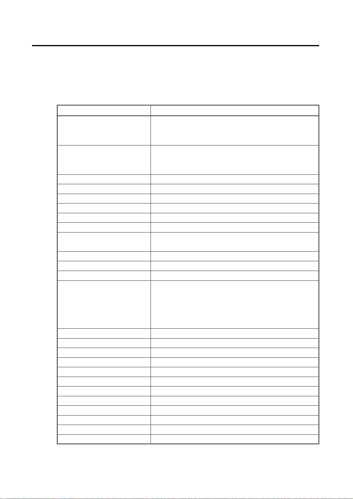
2. PERFORMANCE
- 6 -
2. PERFORMANCE
2.1 H/W Features
Item Feature
Li-Polymer, 630 mAh
Standard Battery Size: 44××68.6××5.6 mm
Weight: 22 g
Li-Ion, 940 mAh
Extended Battery Size: 44××68.6××8.7 mm
Weight: 32 g
AVG TCVR Current GSM , EGSM: 243 mA, DCS: 209 mA
Stand by Current < 3 mA
Talk time 2.7 hours (GSM TX Level 7)
Stand by time 200 hours (Paging Period:9, RSSI: -85 dBm)
Charging time 2 hours
RX Sensitivity GSM, EGSM: -108 dBm, DCS: -107 dBm
TX output power GSM, EGSM: 32 dBm (Level 5)
DCS: 29.5 dBm (Level 0)
GPRS compatibility Yes
SIM card type 3V only
Display 128 ××128 dots LCD (4 Gray color)
Soft icons
Key Pad
Status Indicator 0 ~ 9, #, *, Navigation Key, Up/Down Side Key
Side Key, Confirm Key, Record Key
Send Key, END/PWR Key
Antenna External
EAR Phone Jack Using I/O connector
PC Synchronization Yes
Speech coding EFR/FR
Data and Fax Yes
Vibrator Yes
Buzzer Yes
Voice Recoding Yes
C-Mike Yes
Receiver Yes
Travel Adapter Yes
Options Hands-free kit, CLA, Data Kit
2. PERFORMANCE
- 7 -
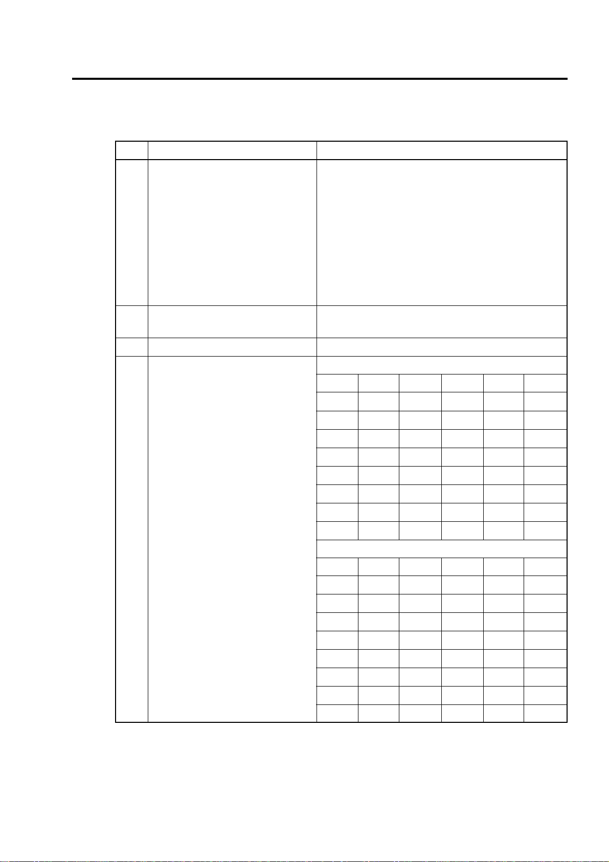
2.2 Technical Specification
Item Description Specification
GSM
TX: 890 + n ××0.2 MHz
RX: 935 + n ××0.2 MHz (n = 1 ~ 124)
EGSM
1 Frequency Band TX: 890 + (n – 1024) ××0.2 MHz
RX: 935 + (n – 1024) ××0.2 MHz (n = 975 ~ 1024)
DCS
TX: 1710 + (n – 512) ××0.2 MHz
Rx: 1805 + (n – 512) ××0.2 MHz (n = 512 ~ 885)
2 Phase Error
RMS < 5 degrees
Peak < 20 degrees
3 Frequency Error < 0.1 ppm
GSM, EGSM
Level Power Toler. Level Power Toler.
5 33 dBm±±2dB 13 17 dBm±±3dB
6 31 dBm±±3dB 14 15 dBm±±3dB
7 29 dBm±±3dB 15 13 dBm±±3dB
8 27 dBm±±3dB 16 11 dBm±±5dB
9 25 dBm±±3dB 17 9 dBm
±±
5dB
10 23 dBm±±3dB 18 7 dBm
±±
5dB
11 21 dBm±±3dB 19 5 dBm
±±
5dB
4 Power Level 12 19 dBm±±3dB
DCS
Level Power Toler. Level Power Toler.
0 30 dBm±±2dB 8 14 dBm±±3dB
1 28 dBm±±3dB 9 12 dBm±±4dB
2 26 dBm±±3dB 10 10 dBm±±4dB
3 24 dBm±±3dB 11 8 dBm
±±
4dB
4 22 dBm±±3dB 12 6 dBm
±±
4dB
5 20 dBm±±3dB 13 4 dBm
±±
4dB
6 18 dBm±±3dB 14 2 dBm
±±
5dB
7 16 dBm±±3dB 15 0 dBm
±±
5dB

2. PERFORMANCE
- 8 -
Item Description Specification
GSM, EGSM
Offset from Carrier (kHz). Max. dBc
100 +0.5
200 -30
250 -33
400 -60
600 ~ 1,200 -60
1,200 ~ 1,800 -60
1,800 ~ 3,000 -63
3,000 ~ 6,000 -65
5 Output RF Spectrum 6,000 -71
(due to modulation)
DCS
Offset from Carrier (kHz). Max. dBc
100 +0.5
200 -30
250 -33
400 -60
600 ~ 1,200 -60
1,200 ~ 1,800 -60
1,800 ~ 3,000 -65
3,000 ~ 6,000 -65
6,000 -73
GSM, EGSM
Offset from Carrier (kHz) Max. (dBm)
400 -19
600 -21
1,200 -21
6 Output RF Spectrum 1,800 -24
(due to switching transient)
DCS
Offset from Carrier (kHz) Max. (dBm)
400 -22
600 -24
1,200 -24
1,800 -27
7 Spurious Emissions
Conduction, Emission Status
Conduction, Emission Status
2. PERFORMANCE
- 9 -
Item Description Specification
GSM, EGSM
8 Bit Error Ratio
BER (Class II) < 2.439% @-102 dBm
DCS
BER (Class II) < 2.439% @-100 dBm
9 RX Level Report Accuracy
±±
3 dB
10 SLR 8±±3 dB
Frequency (Hz) Max.(dB) Min.(dB)
100 -12 200 0 300 0 -12
11 Sending Response 1,000 0 -6
2,000 4 -6
3,000 4 -6
3,400 4 -9
4,000 0 -
12 RLR 2±±3 dB
Frequency (Hz) Max.(dB) Min.(dB)
100 -12 200 0 300 2 -7
500
*
-5
13 Receiving Response 1,000 0 -5
3,000 2 -5
3,400 2 -10
4,000 2
* Mean that Adopt a straight line in between 300 Hz
and 1,000 Hz to be Max. level in the range.
14 STMR 13±±5 dB
15 Stability Margin > 6 dB
dB to ARL (dB) Level Ratio (dB)
-35 17.5
-30 22.5
16 Distortion
-20 30.7
-10 33.3
0 33.7
7 31.7
10 25.5
17 Side tone Distortion Three stage distortion < 10%
18
System frequency (13 MHz) tolerance
≤ 2.5 ppm
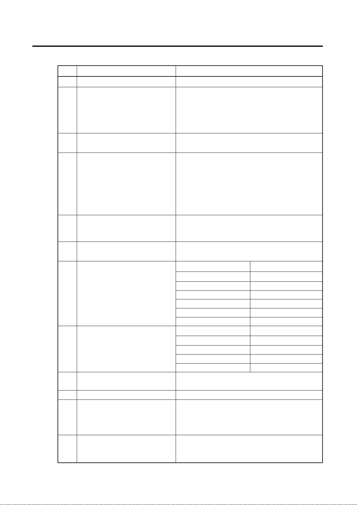
2. PERFORMANCE
- 10 -
Item Description Specification
19 32.768KHz tolerance ≤ 30 ppm
Full power
< 243 mA (GSM, EGSM) ; < 209 mA (DCS)
20 Power Consumption Standby
- Normal ≤ 3 mA (Max. power)
- Using Test mode on DSP Sleep function ≤ 6 mA
21 Talk Time
GSM/ Level 7 (Battery Capacity 630mA): 162 Min
GSM/ Level 12 (Battery Capacity 630mA): 240 Min
Under conditions, at least 200 hours:
1. Brand new and full 630mAh battery
2. Full charge, no receive/send and keep GSM in idle
22 Standby Time mode.
3. Broadcast set off.
4. Signal strength display set at 3 level above.
5. Backlight of phone set off.
At least 80 dB under below conditions:
23 Ringer Volume 1. Ringer set as ringer.
2. Test distance set as 50 cm
24 Charge Voltage
Fast Charge : < 500 mA
Slow Charge: < 60 mA
Antenna Bar Number Power
5 -85 dBm ~
4 -90 dBm ~ -86 dBm
25 Antenna Display 3 -95 dBm ~ -91 dBm
2 -100 dBm ~ -96 dBm
1 -105 dBm ~ -101 dBm
0 ~ -105 dBm
Batter Bar Number Voltage
0 ~ 3.62 V
26 Battery Indicator 1 3.62 ~ 3.73 V
2 3.73 ~ 3.82 V
3 3.82 V ~
27 Low Voltage Warning
3.5 ±±0.03 V (Standby)
3.62 ±±0.03 V (Call)
28 Forced shut down Voltage 3.35 ±±0.03 V
1 Li-Polymer Battery
29 Battery Type
Standard Voltage = 3.7 V
Battery full charge voltage = 4.2 V
Capacity: 630 mAh
Switching-mode charger
30 Travel Charger Input: 100 ~ 240 V, 50/60 Hz
Out put: 5.2 V, 600 mA
3. TECHNICAL BRIEF
- 11 -
3. TECHNICAL BRIEF
3.1 Receiver
The receiver part contains all active circuits for a complete, full receiver chain with the exception of
RF PLL VCO(U302) and discrete RF SAW filters. The filtered and amplified signal is processed from
the RF-mixer inputs to the baseband(BB) output. The receiver path is supported by external channel
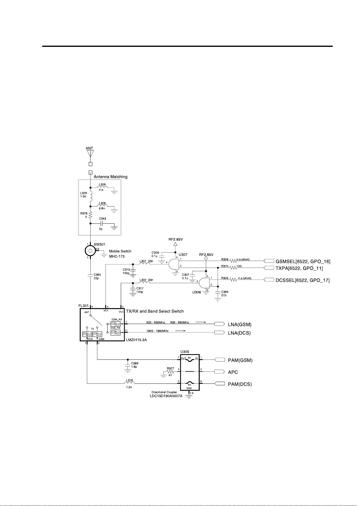
filtering. The RF front-end circuit is shown Fig. 3-1.
Figure 3-1. RF Front-end Circuit.
※※
Note : Please refer to ‘chapter8. Circuit Diagram’ for more details.

3. TECHNICAL BRIEF
- 12 -
A. RF front end
The RF receive signals(GSM 925MHz ~ 960MHz, DCS 1805MHz ~ 1880MHz) are input via the
antenna or coaxial connector. An antenna matching circuit is between the antenna and the
connector.
The FEM(FL301) is used to control the Rx and TX paths. And, the input signals VC1 and VC2 of a
FL301 are connected to 2-Input AND Gates(U306,U307) to switch either TX or RX path on. When
the RX path is turned on, the received RF signal then feeds either LNA(DCS) or LNA(DCS) path
selected by GSM-RX and DCS-RX respectively. This LNA(GSM) path contains one SAW filter,
contained within the FEM(FL301) to filter any unwanted signal apart from the DCS RX band. And,
the LNA(DCS) path is the same case.
Front-end module (LMZ0115-2A) contains an antenna switch module for dual band phone and dual
RF SAW filters. The logic and current is given below Table 3-1.
Table 3-1. The Logic and Current
These two paths are then connected to the GSMB (#6) and DCSB (#10) of HD155128TF (U301),
respectively. The RF receive signal is amplified by LNAs in HD155128TF with the output at GSMC
(#4) and DCSC (#8) respectively, and then pass through the SAW filters B4121 (FL302) and B4133
(FL303).
After this filtering process, the signal then feeds into the first receiver mixer within the HD155128TF
(U301) for mixing with LO, which is produced by the synthesizer Si4133G_XM2 (U302). The mixers
are implemented as Gilbert cells and the first receiver mixer block contains four mixer cells whose
outputs are combined at the MIX1OUT/OUTB pins. The four mixer cells provide high or low
conversion gain at 900MHz or 1800MHz. The two high-gain cells have been optimized for to meet
the System requirements of the receiver at 900MHz and 1800MHz respectively.
On both bands, the gain step between high and low gain operation is around 12dB.
B. IF Part
In U301, UHF mixers produce an IF signal of frequency 225MHz at MIX1OUT (#49) and
MIX1OUTB (#50) in differential mode. This differential signal is filtered by MKFC225 (FL304), a 225
MHz SAW filter, and then fed to U301 IFIN and IFINB (#40 and #41).
The filtered IF signal then feeds into the second receiver mixer within the HD155128TF (U301) for
mixing with a 270 MHz, which was derived from the synthesizer Si4133G_XM2 (U302), and
generates a 45 MHz IF signal.
The 45 MHz output from the second mixer is filtered and passes to the PGA. The gain of the PGA is
set by a 6-bit programming word supplied by the BB. A further two bits are used to control
independently the gain steps in the first receive mixer and the IF amplifier/second mixer. The PGA
gain step size is nominally 2dB and the usable control range is 96 dB.
VC1 VC2 Current
GSM TX 2.7 V 0 V 10.0 mA max
DCS TX 0 V 2.7 V 10.0 mA max
GSM/DCS RX 0 V 0 V < 0.1 mA
3. TECHNICAL BRIEF
- 13 -
C. RX I/Q Demodulator
The amplified IF signal at 45 MHz passes to the demodulator and is mixed down to DC to generate
I and Q BB signals. The BB signals pass via integrated low-pass filters to the BB A/D converters.
The remainder of the channel filtering is performed by the BB chipset. The demodulator contains
switches to maintain the sense of the BB I/Q outputs with respect to the incoming RF signal on both
GSM900 and DCS1800. It is not necessary to invert the receive data within the BB when switching
between 900MHz and 1800MHz. Fig. 3-2 shows RX path circuit.
Figure 3-2. RX Path Circuit.
Table 3-2. Gain and Noise Figure of RX Path.
Table 3-3. Total Gain and Noise Figure of RX Path.
Front End Module LAN RF SAW Filter Mixerl IF SAW Filter Mixer2
Gain GSM -2.9 17 -2.8 9.5 -6.5 14
DCS -3.5 16 -3.1 10.5
NF(dB) GSM 1.5 9.5 7
DCS 1.8 9.5
Total Gain Total Noise Figure
GSM, EGSM 28.3 dB 5.33 dB
DCS 27.4 dB 6.62 dB
3. TECHNICAL BRIEF
- 14 -
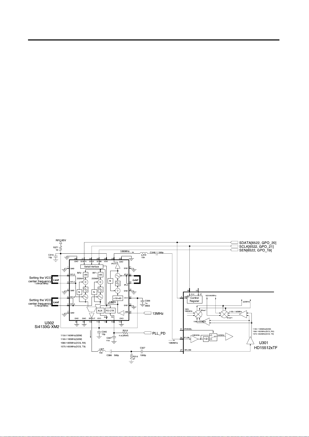
3.2 Synthesizer
The synthesizer IC, the Si4133G-XM2, comprises three complete PLLs. One, which is active all of
the time and in this application produces a constant 1080MHz. This is the IF oscillator and is divided
down inside the HD 155128 to produce the 270 MHz for the second receive mixer, and with an
optional further division to 135 MHz for the transmitter quadrature modulator. The two remaining
synthesizers provide HD 155128 with the RFLO for GSM900 and DCS1800 bands.
The synthesizers use a number of techniques to improve lock times, making them well suited to
GPRS. The use of two synthesizers switched makes the Si4133G-XM2 dual band compatible whilst
minimizing the size of the IC. A fixed reference frequency of 1 MHz is generated by a reference
divider from the external applied 13 MHz crystal oscillator. The phase frequency detector with
charge pump output provides programmable output current drive capability and pulse width.
The counter and mode settings of the synthesizer are also programmed via 3-wire interface.
Table 3-4. Synthesizer 3-wire Bus.
The PLLs can adjust the IF and RF output frequencies ( 5 % with respect to their VCO center
frequencies. Each center frequency is established by the value of an external inductance connected
to the respective VCO. Because the inductances are in the low nH range, the inductance of the
package needs to be considered in determine the correct external inductance. The total inductance
(Ltot)presented to each VCO is the sum of the external inductance (Lext) and the package
inductance (Lpkg). Each VCO has a nominal capacitance (Cnom) in parallel with the total
inductance, and the center frequency is as follows:
Fcen = (3-1)
or,
Fcen = (3-2)
Table 3-5. External Inductance.
Pin Number Description
SDATA 27 Serial data input to the synthesizer IC
SCLK 26 Serial clock input to the synthesizer IC
SENB 25 Input latches the serial data transferred to the synthesizer IC
Inductance
RF1 VCO 0.758 nH
RF2 VCO 2.37 nH
IF VCO 1.74 nH
1
2π√Ltot xCnom
1
2π√(Lpkg + Lext) xCnom
3. TECHNICAL BRIEF
- 15 -
Table 3-6. Si4133G-XM2 VCO Characteristics.
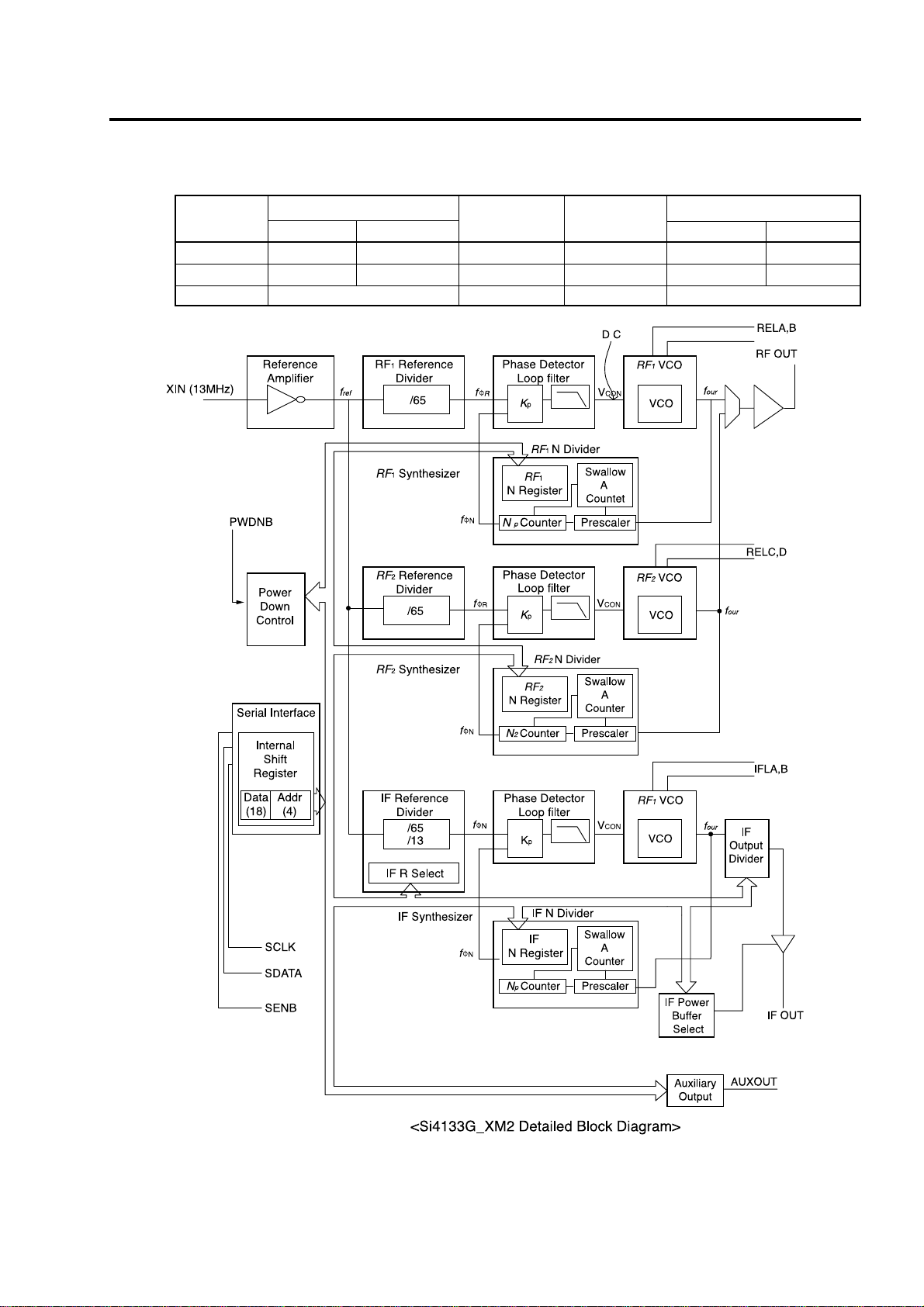
Figure 3-3. Synthesizer Internal Block Diagram.
Fcen Range (MHz)
Cnom ( pF ) Lpkg ( nH )
Lext Range ( nH )
Min Max Min Max
RF1 947 1720 4.3 1.5 0.5 5.1
RF2 789 1429 4.8 1.5 1.1 7.0
IF 1080 6.5 1.6 1.7
3. TECHNICAL BRIEF
- 16 -
The IF and RF output frequencies are set by programming the N Divider registers. All three PLL R
Dividers are fixed at R = 65 to yield a 200 kHz phase detector update rate from a 13 MHz reference
frequency.
Fout/N = Fref/65 (3.3)
For XIN = 13 MHz, Fout = N x 200 kHz
RF1 VCO(DCS)Frequency range : TX : 1,550 ~ 1,650 MHz, RX : 1,580 ~ 1,655 MHz
RF1 VCO(DCS)Frequency range : TX, RX : 1,150 ~ 1,185 MHz
IF VCO : 1,080 MHz
The RFOUT and IFOUT pins are driven by amplifiers that buffer the RF VCOs and IF VCO,
respectively. The RF output amplifier receives its input from either the RF1 or RF2 VCO, depending
upon which N divider register was last written to.
The RFOUT pin must be coupled to its load through an ac coupling capacitor. A matching network is
required to maximize power delivered into a 50 Ω load. The network is made to provide an adequate
match to an external 50ohm load for both the RF1 and RF2 frequency bands. The matching network
also filters the output signal to reduce harmonic distortion.
The RF output power is controlled with the RFPWR bit in register 0. Setting this bit increases the
supply current by approximately 1.2 mA.
The IFOUT pin must also be coupled to its load through an ac coupling capacitor. A matching
network is also required in order to drive a 50 Ω load.
Depending on transceiver requirements, the matching network may not be needed.
Figure 3-4. Synthesizer Circuit.

3. TECHNICAL BRIEF
- 17 -
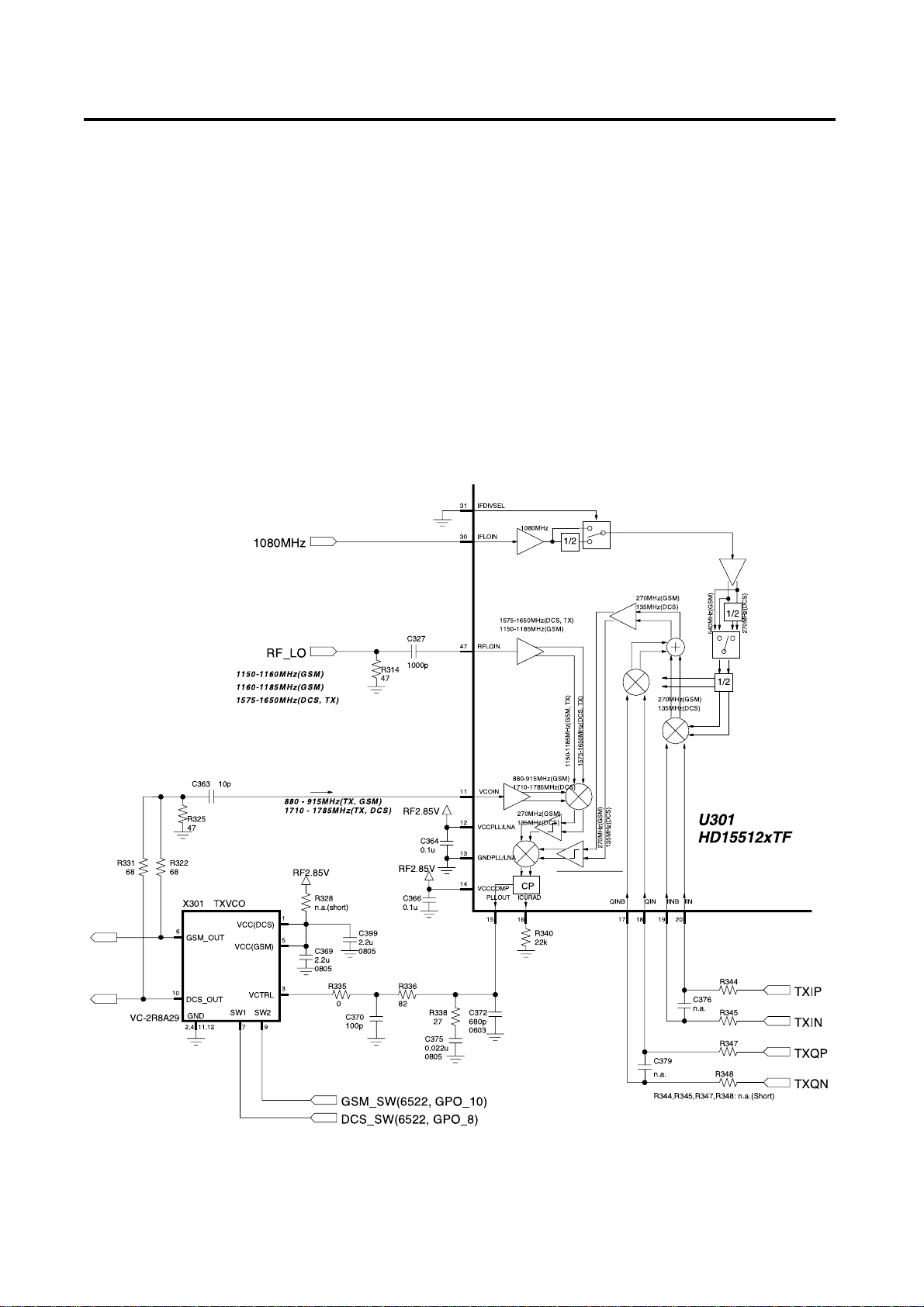
3.3 Transmitter
The Transmitter part contains HD155128TF active parts and PAM, APC IC, coupler, FEM(front-end
module) circuit. The HD155128TF active part consists of a vector modulator and offset phaselocked loop block(OPLL) including down-converter, phase detector, loop filter and dual band
transmit VCO which can operate at either final RF output frequency. The RF GMSK outputs from
the transmit VCO are fed directly to the RF power amplifiers. The peak output power and the profile
of the transmitted burst are controlled by means of a closed feedback loop. A dual band directional
coupler is used to sample the RF output from either PA. The PA outputs from the directional coupler
pass to the antenna connector via an integrated dual band front-end module.
Figure 3-5. Transmitter Block Diagram.
3. TECHNICAL BRIEF
- 18 -
A. TX IF Modulator
The TX I and Q signals from BB analog chipset, AD6521(U2), #F9, E9, C9, D9 are fed to #17~20 of
the HD155128TF TX modulator(U301), where they are then modulated onto either a TX IF of
270MHz(for GSM-TX) or 135MHz(for DCS-TX) by the quadrature mixer inside U301. The signal TX
LO IF(270MHz,135MHz) is input from U301. This signal is produced by the external 1,080 MHz IF
VCO of synthesizer Si4133G_XM2(U302), which has been divided down by a factor of 4 for GSMTX or 8 for DCS-TX. This division factor is set by the control signal of BB digital chipset,
AD6522(U3) #D14, D13, F11.
The modulator provides more than 40 dBc of carrier and unwanted side-band rejection and
produces a GMSK modulated signal. The BB software is able to cancel out differential DC offsets in
the I/Q BB signals caused by imperfections in the D/A converters. The TX-Modulator implements a
quadrature modulator. The IF-frequency input signal is split into two precise orthogonal carriers,
which are multiplied by the BB modulation signal IT/ITX and QT/QTX. It is used as reference signal
for the OPLL.
Figure 3-6. TX IF Modulator and OPLL Circuit.

3. TECHNICAL BRIEF
- 19 -
B. OPLL
The down converter contained inside of the HD155128TF (U301) mixes the TX RF frequency with
the RF VCO signal from the Si4133G-XM2 (U302) to generate a `feedback' signal at 270 MHz for
GSM and EGSM operation or 135 MHz for DCS operation. The `feedback' signal passes via a
limiter to one port of the phase detector.
The GMSK reference signal from the TX IF modulator passes via a second limiter to the other input
port of the phase detector. The phase detector generates an error current proportional to the phase
difference between the `feedback` signal from the down-converter and the `reference' signal from
the TX IF modulator.
The error current is filtered by a second order low-pass filter to generate an output voltage, which
depends on the GMSK modulation and the desired channel frequency. This voltage controls the
transmit VCO such that the VCO output signal, centered on the correct RF channel is frequency
modulated with the original GMSK data.
The center frequency of the transmit VCO is offset from the RF VCO frequency by 270 MHz for
GSM and EGSM operation or 135 MHz for DCS operation.
Hence:
GSM TX = RF VCO – 270, i.e., (1,150 – 270 = 880 MHz) (3.4)
DCS TX = RF VCO + 135, i.e., (1,575 + 135 = 1,710 MHz) (3.5)
The OPLL acts as a tracking narrowband band pass filter tuned to the desired channel frequency.
This reduces the wideband noise floor of the modulation and up-conversion process and provides
significant filtering of spurious products
C. Power Amplifier
The PF08107B [U303] is Dual band power amplifier for EGSM (880 to 915 MHz) and DCS (1,710 to
1,785 MHz). The efficiency of module is the 50 % at nominal output power for EGSM and the 43 %
at 32 dBm for DCS. For 3.5 V nominal battery use.
This module should be operated under the GSM burst pulse. To avoid permanent degradation, CW
operation should not be applied. To avoid the oscillation at no input power, before the input is cut
off, the control voltage Vapc should be control to less than 0.5 V. We have to improve thermal
resistance, the through holes should be layouted as many as possible on PCB under the module.
And to get good stability, all the GND terminals and the metal cap should be soldered to ground
plane of PCB.

3. TECHNICAL BRIEF
- 20 -
Figure 3-7. Power Amplifier and its Control Part Circuits.
D. PA Circuit and Control
The power amplifier control circuit ensures that the RF signal is regulated to the required limits of
operation.
RF power is controlled by driving the power control pins of power amplifier and sensing the
resultant RF output power via a directional coupler (U305). The RF sense voltage is peak detected
using an on-chip Schottky diode inside of AD8315(U304). This detected voltage is compared to the
DAC voltage at the VSET pin of APC IC (U304) to control the output power.
An internal input signal(TXRAMP) from AD6521(U2) is applied to the positive input of the APC
IC(U304) during the TXEN mode and a directional coupler near the antenna feeds a portion of the
RF output signal back to the APC IC(U304) and peak detector converts this signal to a low
frequency feedback signal that balances the amplifier when this signal equals the RAMP input
signal level.
3. TECHNICAL BRIEF
- 21 -
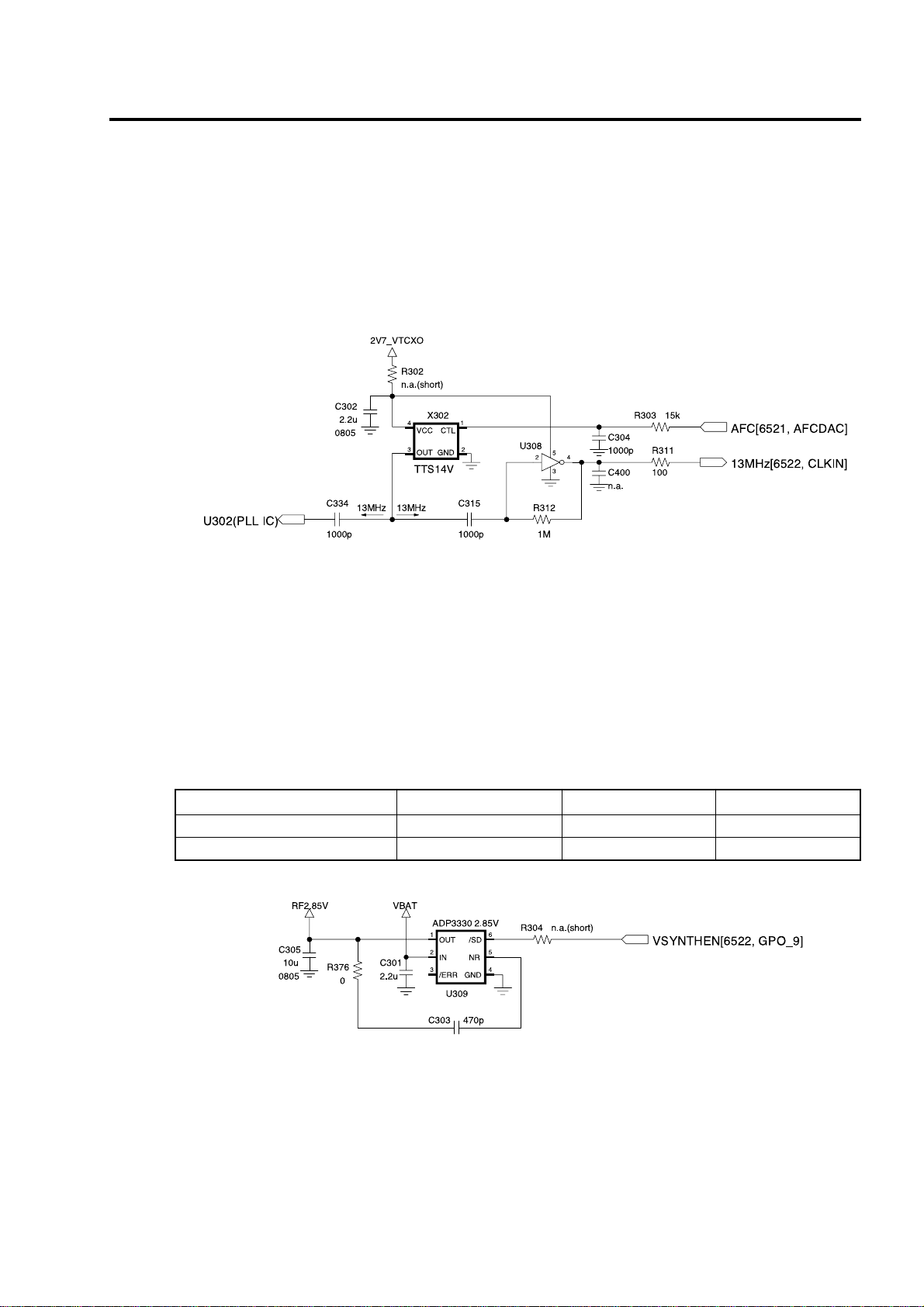
3.4 13MHz Clock
The 13 MHz clock (VC-TCXO-208C) consists of a TCXO (Temperature Compensated Crystal
Oscillator) which oscillates at a frequency of 13 MHz.
It is used within the Si4133G_XM2 Synthesizers, BB Analog chip-set (AD6521), and Digital
(AD6522). The inverter IC, SN74AHC1GU04 buffer the output to AD6521, AD6522 and
Si4133G_XM2.
Figure 3-8. VCTCXO Circuit.
3.5 Power Supplies and Control Signals
There are two regulators used in the phone to provide RF power. One is contained inside of
ADP3408 (U1), power management IC to provide the power for the VCTXO (X302). The other is
used to provide the power for remaining RF circuits.
Table 3-7. Power Supplies
Figure 3-9. Regulator Circuit.
Regulator Voltage Powers Enable Signal
Regulator 1 (U1, 2V7_VTCXO) 2.7 V ±±0.5 V VCTXO
Regulator 2 (U309, RF2V8) 2.85 V ±±0.5 V RF circuitry VSYNTHEN
3. TECHNICAL BRIEF
- 22 -
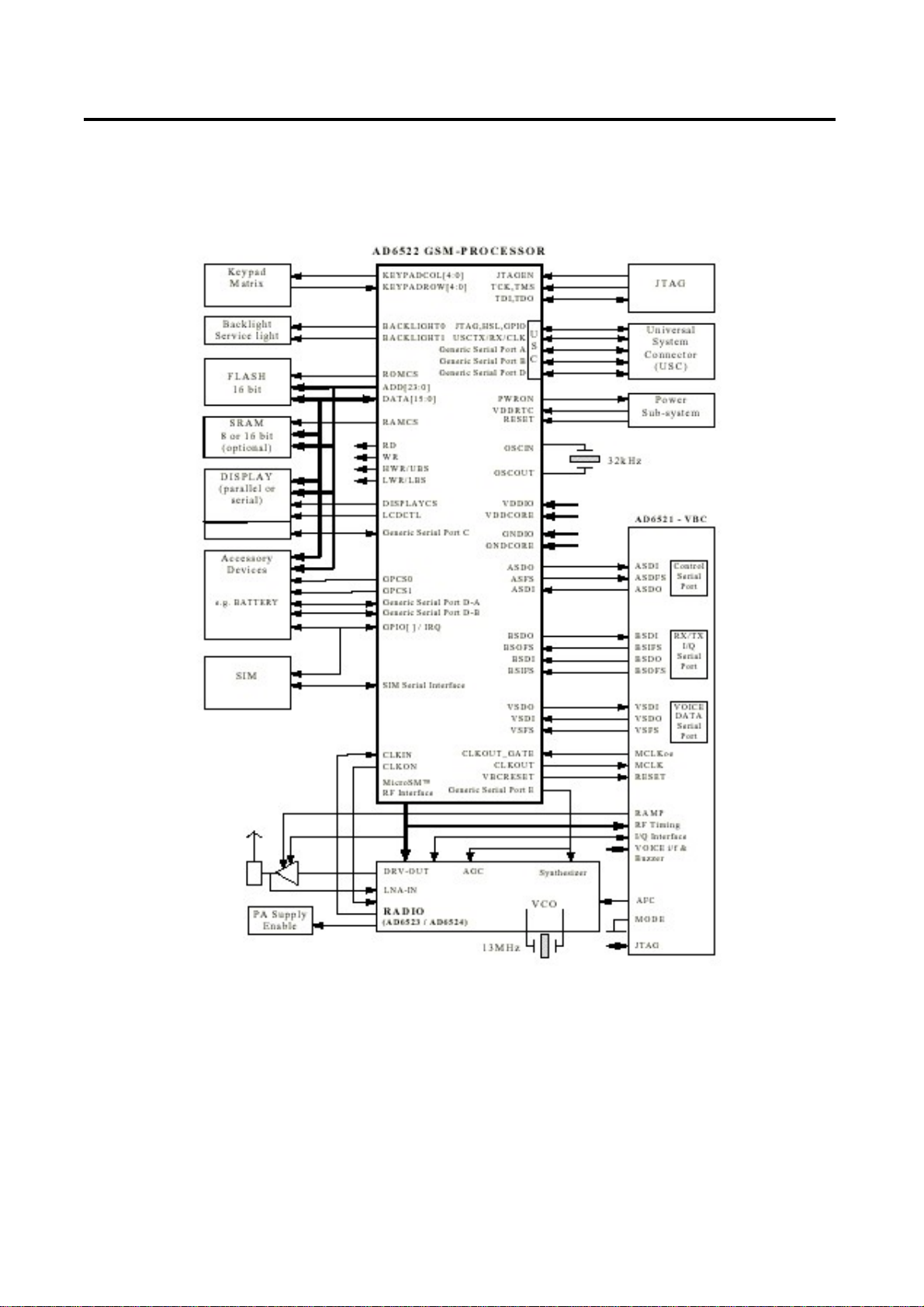
3.6 Digital Main Processor
Figure 3-10. System Interconnection of the AD6522 External Interfaces
3. TECHNICAL BRIEF
- 23 -
Interconnection with external devices
A. RTC block interface
Countered by external X-TAL
The X-TAL oscillates 32.768KHz
B. LCD module interface
Controlled by LCD_CS, LCD_RES, LCD_A0, /WR, /RD, DATA [00...07] ports
Table 3-8. LCD Module Interface.
C. RF interface
The AD6522 control RF parts through TXEN, RXON1, RXON2, AGCEN, SDATA, SCLK, SEN etc.
Table 3-9. RF Interface.
Description
LCD_CS LCD chip enable
LCD_RES This pin resets LCD module
LCD_A0
This pin determines whether the data to LCD module is display data or control data
/WR, /RD Read/Write control
DATA [00...07] Parallel data line
Signal Name Description
TXEN TX Enable/Disable
RXON1 LNA, Mixer1 On/Off
RXON2 Mixer 2 On/Off
AGCEN AGC Enable/Disable
SDATA Serial Data to PLL
SCLK Clock to PLL
SEN PLL Enable/Disable
3. TECHNICAL BRIEF
- 24 -
D. SIM interface
The AD6522 check status periodically in call mode if SIM card is inserted or not , but the AD6522
don't check in deep sleep mode.
Interface by SIM_IO, SIM_CLK, SIM_RST
Table 3-10. SIM Interface.
Figure 3-11. SIM Circuit.
E. Key interface
Include 5 column and 5 row.
The AD6522 detect key press by interrupt.
F. AD3408 interrupt
There are two interrupts EOC and CHARGERDETECT
EOC: End Of Charge. Charging would be stopped when AD6522 receive this interrupt.
CHARGERDETECT: This interrupt is generated when charger is inserted.
Description
SIM_IO
This pin receives and sends data to SIM card. LG-512W support only 3.0 volt
interface SIM card.
SIM_CLK Clock 3.5MHz frequency
SIM_RST Reset SIM block

3. TECHNICAL BRIEF
- 25 -
3.7 Analog Main Processor
A. Baseband Transmit section
This section generates in-phase and quadrature BB modulated GMSK signals (BT = 0.3) in
accordance with GSM 05.05 Phase 2 specifications.
The transmit channel consists of a digital GMSK modulator, a matched pair of 10-bit DACs and a
matched pair of reconstruction filter.
B. Baseband Receive section
This section consists of two identical ADC channels that process baseband in-phase(I) and
quadrature(Q) input signals.
Each channel consists of a coarse switched capacitor input filter, followed by a high-order sigmadelta modulator and a lowpass digital filter.
C. Auxiliary section
This section contains two auxiliary DACs(AFC DAC, IDAC) for system control.
This section also contains AUX ADC and Voltage Reference.
AUX ADC: 6 channel 10 bits
AFC DAC: 13 bits
IDAC: 10 bits
D. Voiceband section
Receive audio signal from MIC. LG-512W use differential configuration.
Send audio signal to Speaker. LG-512W use differential configuration.
It interconnect with external device like main microphone, main speaker, ear-phone and Hands free
kit through the VINNORP, VINNORN, VOUTNORP, VOUTNORN, VINAUXP, VINAUXN,
VOUTAUXP, VOUTAUXN and BUZZER port.
VINNORP, VINNORN: Main MIC positive/negative terminal
VOUTNORP, VOUTNORN: Main Speaker positive/negative terminal
VINAUXP, VINAUXN: Hands free kit mike positive/negative terminal
VOUTAUXP, VOUTAUXON: Hands free kit speaker positive/negative terminal
BUZZER: Buzzer Output terminal
3. TECHNICAL BRIEF
- 26 -
3.8 Power Management
ADP3408
Figure 3-12. ADP3408 Inner Block Diagram.

3. TECHNICAL BRIEF
- 27 -
A. Power up sequence logic
The ADP3408 controls power on sequence.
B. Power on sequence
If a battery is inserted, the battery powers the 6 LDOs.
Then if PWRONKEY is detected, the LDOs output turn on.
REFOUT is also enabled.
Reset is generated and send to the AD6522.
C. LDO block
There are 6 LDOs in the ADP3408.
Table 3-11. LDO Block.
D. Battery charging block
It can be used to charge Lithium Ion and/or Nickel Metal Hydride batteries. LG-512W use Li-Ion and
Li-polymer battery only.
Charger initialization, trickle charging, and Li-Ion charging control are implemented in hardware.
E. Charging Process
Check charger is inserted or not.
If ADP3408 detects that Charger is inserted, the CC-CV charging starts.
Exception: When battery voltage is lower than 3.2V, the precharge (low current charge mode) starts
firstly.
And the battery voltage reach to 3.2V the CC-CV charging starts.
F. Pins used for charging
CHARGERDETECT: Interrupt to the AD6522 when charger is plugged.
CHARGEEN: Control signal from the AD6522 to charge Li+ battery .
EOC: Interrupt to the AD6522 when battery is fully charged.
GATEIN: Control signal from AD6522 to charge NiMH battery. But, not used.
MVBAT: Battery voltage divider. Divide ratio is 1:2.3 and it is sensed in AD6521 AUX_ADC.
Description
VSIM 2.86 V (is provided to SIM card)
VCORE 2.45 V (is provided to the AD6522 and AD6521's digital core)
VRTC 2.45 V (is provided to the RTC and Backup Battery)
VAN 2.45 V (is provided to the AD6521 I/O and used as microphone bias)
VTCXO 2.715 V (is provided to VCTCXO)
VMEM 2.80 V (is provided to Flash)
3. TECHNICAL BRIEF
- 28 -
G. TA (Travel Adaptor)
Input voltage: AC 85 V ~ 260 V, 50~60 Hz
Output voltage: DC 5.2 V ( ±±0.2 V )
Output current: Max 850 mA ( ±±50 mA )
H. Battery
Li-polymer and Li-ion battery (Max 4.2 V, Nom 4.0 V)
Standard battery: Capacity - 630 mAh, Li-polymer
Extended battery (Optional): Capacity - 940 mAh, Li-Ion
3.9 Memories
32M flash memory + 4M SRAM
16 bit parallel data bus
ADD01 ~ ADD21
RF Calibration data art stored in Flash (LG-512W do not use EEPROM)
3.10 Display and Interface
Table 3-12. LCD Module.
There is the control output LCD_CS which is derived from the AD6522, this acts as the chip select
enable for the LCD module. AD6522 uses DATA[00:07] pins to send data for displaying graphical
text onto the LCD
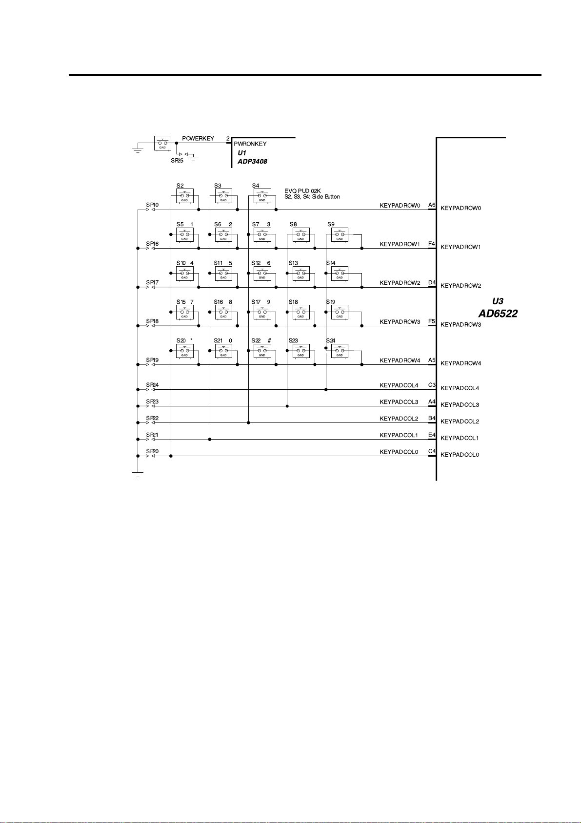
3.11 Keypad Switches and Scanning
The key switches are metal domes, which make contact between two concentric pads on the
keypad layer of the PCB when pressed. There are 24 switches (S1~S24), connected in a matrix of
5 rows by 5 columns, as shown in Figure, except for the power switch (S1), which is connected
independently. Functions, the row and column lines of the keypad are connected to ports of the
AD6522. The columns are outputs, while the rows are inputs and have pull-up resistors built in.
When a key is pressed, the corresponding row and column are connected together, causing the
row input to go low and generate an interrupt. The columns/rows are then scanned by the AD6522
to identify the pressed key.
Description
Display format 128 x 128 dots
Back light EL backlight
3. TECHNICAL BRIEF
- 29 -
Figure 3-13. Keypad Switches and Scanning.
 Loading...