

LG 50PM4700-TA Schematic

Internal Use Only
North/Latin America http://aic.lgservice.com
Europe/Africa http://eic.lgservice.com
Asia/Oceania http://biz.lgservice.com
PLASMA TV
SERVICE MANUAL
CHASSIS : PA22A
MODEL : 50PM4700 50PM4700-TA
CAUTION
BEFORE SERVICING THE CHASSIS,
READ THE SAFETY PRECAUTIONS IN THIS MANUAL.
Printed in KoreaP/NO : MFL67341704 (1201-REV00)

CONTENTS
CONTENTS .............................................................................................. 2
SAFETY PRECAUTIONS ........................................................................ 3
SPECIFICATION ....................................................................................... 4
ADJUSTMENT INSTRUCTION ................................................................ 6
BLOCK DIAGRAM .................................................................................. 10
EXPLODED VIEW .................................................................................. 11
SCHEMATIC CIRCUIT DIAGRAM ..............................................................
Only for training and service purposes
- 2 -
LGE Internal Use OnlyCopyright © LG Electronics. Inc. All rights reserved.
AC Volt-meter
SAFETY PRECAUTIONS
IMPORTANT SAFETY NOTICE
Many electrical and mechanical parts in this chassis have special safety-related characteristics. These parts are identified by in the
Schematic Diagram and Exploded View.
It is essential that these special safety parts should be replaced with the same components as recommended in this manual to prevent
Shock, Fire, or other Hazards.
Do not modify the original design without permission of manufacturer.
General Guidance
An isolation Transformer should always be used during the
servicing of a receiver whose chassis is not isolated from the AC
power line. Use a transformer of adequate power rating as this
protects the technician from accidents resulting in personal injury
from electrical shocks.
It will also protect the receiver and it's components from being
damaged by accidental sh orts of the cir cui try that may be
inadvertently introduced during the service operation.
If any fuse (or Fusible Resistor) in this TV receiver is blown,
replace it with the specified.
When replacing a high wattage resistor (Oxide Metal Film Resistor,
over 1 W), keep the resistor 10 mm away from PCB.
Keep wires away from high voltage or high temperature parts.
Before returning the receiver to the customer,
always perform an AC leakage current check on the exposed
metallic parts of the cabinet, such as antennas, terminals, etc., to
be sure the set is safe to operate without damage of electrical
shock.
Leakage Current Cold Check(Antenna Cold Check)
With the instrument AC plug removed from AC source, connect an
electrical jumper across the two AC plug prongs. Place the AC
switch in the on position, connect one lead of ohm-meter to the AC
plug prongs tied together and touch other ohm-meter lead in turn to
each exposed metallic parts such as antenna terminals, phone
jacks, etc.
If the exposed metallic part has a return path to the chassis, the
measured resistance should be between 1 M
When the exposed metal has no return path to the chassis the
reading must be infinite.
An other abnormality exists that must be corrected before the
receiver is returned to the customer.
Ω and 5.2 MΩ.
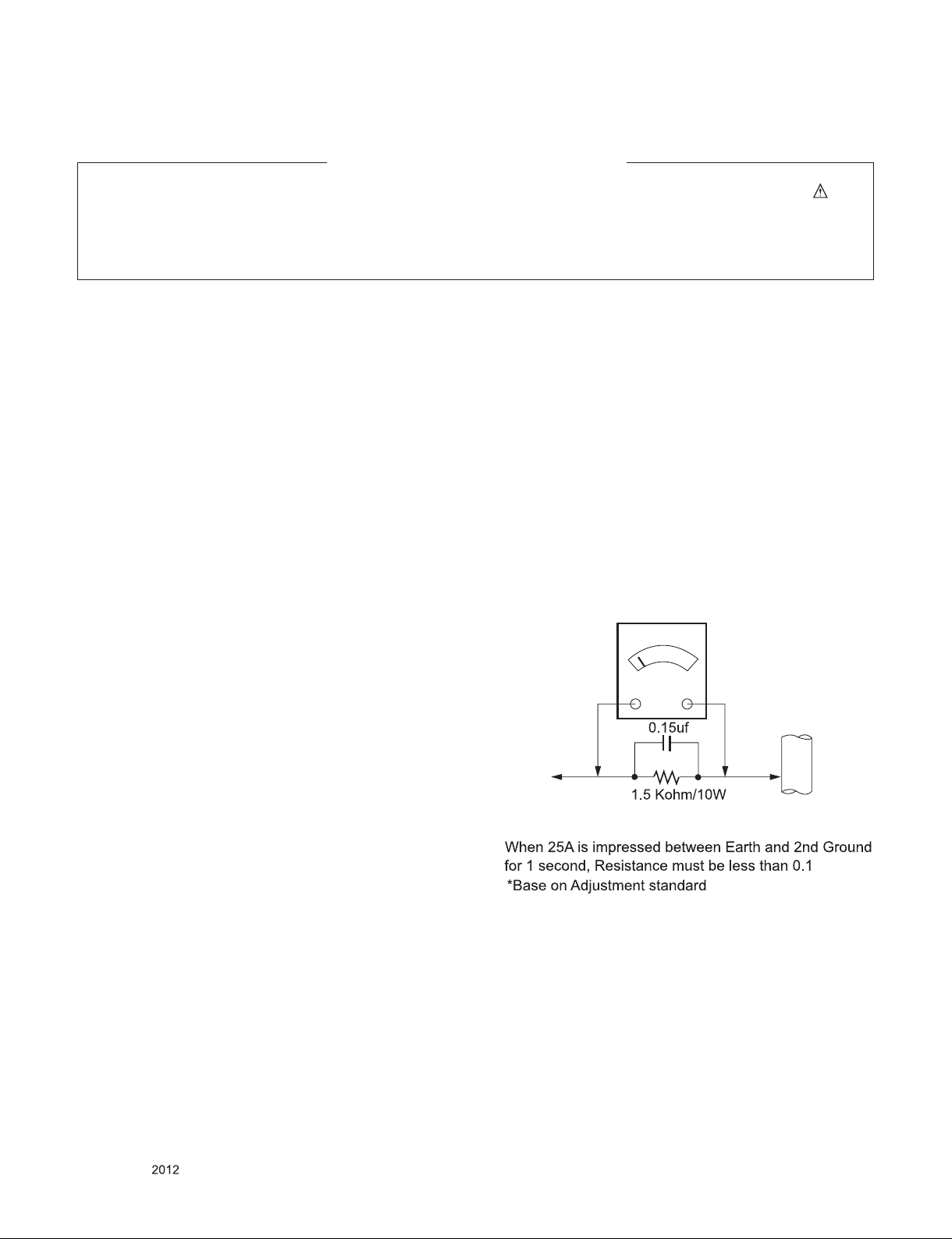
Leakage Current Hot Check (See below Figure)
Plug the AC cord directly into the AC outlet.
Do not use a line Isolation Transformer during this check.
Connect 1.5 K / 10 watt resistor in parallel with a 0.15 uF capacitor
between a known good earth ground (Water Pipe, Conduit, etc.)
and the exposed metallic parts.
Measure the AC voltage across the resistor using AC voltmeter
with 1000 ohms/volt or more sensitivity.
Reverse plug the AC cord into the AC outlet and repeat AC voltage
measurements for each exposed metallic part. Any voltage
measured must not exceed 0.75 volt RMS which is corresponds to
0.5 mA.
In case any measurement is out of the limits specified, there is
possibility of shock hazard and the set must be checked and
repaired before it is returned to the customer.
Leakage Current Hot Check circuit
Good Earth Ground
such as WATER PIPE,
To Instrument's
exposed
METALLIC PARTS
CONDUIT etc.
Only for training and service purposes
- 3 -
LGE Internal Use OnlyCopyright © LG Electronics. Inc. All rights reserved.
SPECIFICATION
NOTE : Specifications and others are subject to change without notice for improvement
1. Application range
This spec sheet is applied all of the PDP TV with PA22A chassis.
2. Requirement for Test
Each part is tested as below without special appointment.
(1) Temperature: 25 °C ± 5 °C(77 °F ± 9 °F), CST: 40 °C ± 5 °C
(2) Relative Humidity: 65 % ± 10 %
(3) Power Voltage
: Standard input voltage (AC 100-240 V~, 50/60 Hz)
* Standard Voltage of each products is marked by models.
(4) Specification and performance of each parts are followed each drawing and specification by part number in accordance with
BOM.
(5) The receiver must be operated for about 5 minutes prior to the adjustment.
3. Test method
(1) Performance: LGE TV test method followed
(2) Demanded other specification
- Safety : CE, IEC specification
- EMC : CE, IEC
4. Module General Specification
- 50" 3D HD
No Item Specication Remark
1 Display Screen Device 127 cm (50 inch) wide Color Display Module PDP
2 Aspect Ratio 16:9
3 PDP Module PDP50T4####,
RGB Closed (Well) Type, Glass Filter (43%)
Pixel Format: 1024 horiz. By 768 ver.
4 Operating Environment 1) Temp. : 0 ~ 40 deg
2) Humidity : 20 ~ 80%
5 Storage Environment 1) Temp. : -20 ~ 60 deg
2) Humidity : 10 ~ 90 %
6 Input Voltage AC100 ~ 240V, 50/60Hz Maker LG
.
LGE SPEC
Only for training and service purposes
- 4 -
LGE Internal Use OnlyCopyright © LG Electronics. Inc. All rights reserved.
5. Model General Specification
No Item Specication Remark
1 Market Australia, New Zealand, Indonesia, Malaysia, Singapore,
Vietnam, South Africa, Iran, Kenya, Israel
2 Broadcasting system 1) PAL BG
2) PAL DK
3) PAL I / II
4) DVB T
3 Receiving system Analog : Upper Heterodyne
Digital : COFDM
4 AV (1EA) PAL
5 Component Input (1EA) Y/Cb/Cr, Y/Pb/Pr
6 RGB Input (1EA) RGB-PC Analog (D-Sub 15Pin)
7 HDMI Input (4EA) HDMI-PC
HDMI-DTV
8 Audio Input (2EA) RGB/DVI Audio, Component L/R Input
9 SPDIF Out (1 EA) SPDIF Out
10 USB (2EA) For SVC, S/W Download, X-Studio, DivX
11 Ethernet LAN(1EA)
► DVB-T
- Guard Interval(Bitrate_Mbit/s)
1/4, 1/8, 1/16, 1/32
- Modulation : Code Rate
QPSK : 1/2, 2/3, 3/4, 5/6, 7/8
16-QAM : 1/2, 2/3, 3/4, 5/6, 7/8
64-QAM : 1/2, 2/3, 3/4, 5/6, 7/8
HDMI1/DVI, HDMI2, HDMI3
Only for training and service purposes
- 5 -
LGE Internal Use OnlyCopyright © LG Electronics. Inc. All rights reserved.
ADJUSTMENT INSTRUCTION
1. Application Range
This spec. sheet applies to PA22A chassis applied PDP TV all
models manufactured in TV factory.
2. Specification
(1) Because this is not a hot chassis, it is not necessary to
use an isolation transformer. However, the use of isolation
transformer will help protect test instrument.
(2) Adjustment must be done in the correct order.
(3) The adjustment must be performed in the circumstance of
25 °C ± 5 °C of temperature and 65±10% of relative
humidity if there is no specific designation.
(4) The input voltage of the receiver must keep 100~240V,
50/60Hz.
(5) The receiver must be operated for about 5 minutes prior to
the adjustment when module is in the circumstance of over
15 °C
- In case of keeping module is in the circumstance of 0°C, it
should be placed in the circumstance of above 15°C for 2
hours
- In case of keeping module is in the circumstance of below
-20 °C, it should be placed in the circumstance of above 15
°C for 3 hours,.
3.2. DFT Process
* Depend on situation, Step can be changed.
■ After RGB Full White in HEAT-RUN Mode, the receiver must
be operated prior to the adjustment.
■ Enter into HEAT-RUN MODE
1) Press the POWER ON KEY on R/C for adjustment.
2) OSD display and screen display PATTERN MODE.
● Set is activated HEAT run without signal generator in this
mode.
● Single color pattern ( WHITE ) of HEAT RUN MODE uses to
check panel.
● Caution : If you turn on a still screen more than 20 minutes
(Especially digital pattern, cross hatch pattern), an
after image may be occur in the black level part of
the screen.
3. PCB Assembly adjustment
* Caution : Using ‘power on’ button of the control R/C power on
TV
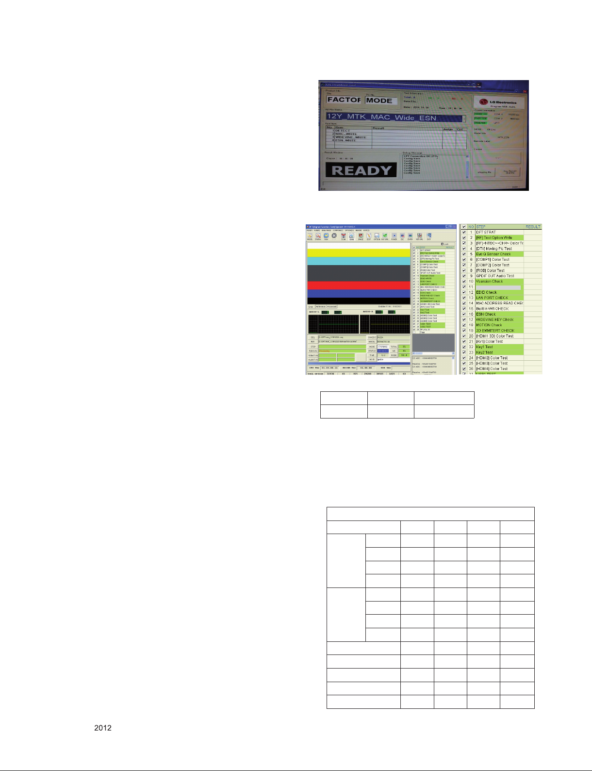
3.1. MAC Address and ESN and Wide-vine
Key Download
* The CI+ Key download is need for only PD22A/B/C Models.
* Connect TV SET and PC which download keys Writing
program by RS232C-Cable
(1) Start Program and Click ‘start’ Button to connect TV and
PC.
(2) When download succeed, you can see “OK” on the
screen.
* Each Chassis has it’s own MAC Address/ESN/Wide-vine
key. Please be careful of download.
* Condition spec
Mode Volume Power Off
RF 0 DC On
3.3. Tool OPTION (MANUAL)
(1) Press ADJ key on R/C to insert Tool OPTION
(2) On the “ Tool Option ”, Insert Tool Option by a number key
(3) Press the ENTER(■)
(4) Press ENTER(■) again.
(5) Select “OK to Download” by using ◄/►(VOL +/-) and
press ►(VOL +)
* PA22A
Model Name PM970 PM690 PM670 PM470
Tool
option 1
Tool
option 2
Tool option 3 973 973 973 845
Tool option 4 29294 29294 29294 29294
Tool option 5 47703 47703 47703 14933
Tool option 6 1561 1561 1561 1561
Tool option 7 8235 9259 8235 8235
42 HD 33062
50 HD 33064
50 FHD 32808 32904 32936
60 FHD 32810 32906 32938
42 HD 391
50 HD 391
50 FHD 390 390 390
60 FHD 390 390 390
Only for training and service purposes
- 6 -
LGE Internal Use OnlyCopyright © LG Electronics. Inc. All rights reserved.
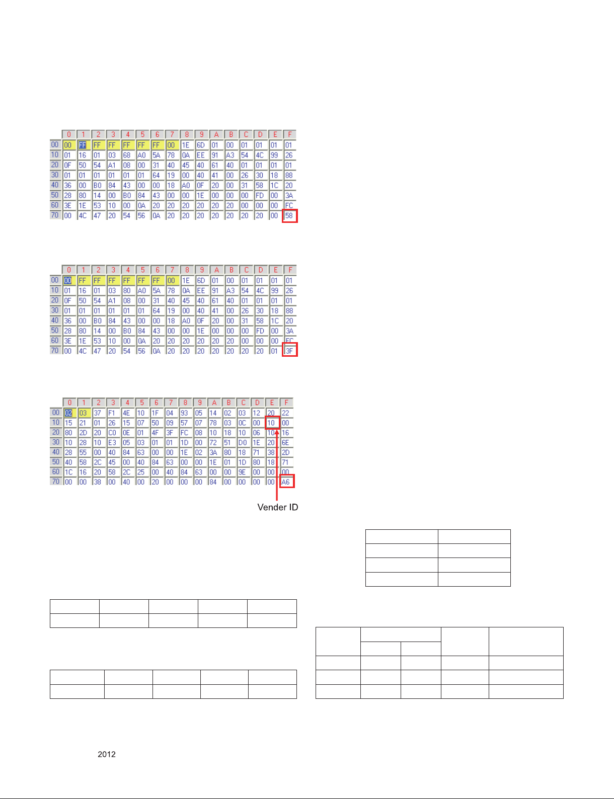
3.4. EDID (The Extended Display Identification Data)
■ RGB [C/S: 58] : For HD Models
EDID Block 0, Bytes 0-127 [00H-7FH]
Block Type: EDID 1.3
4. SET assembly adjustment method
* Caution: Each PCB assembly must be checked by check
JIG set. (Because power PCB Assembly damages
to PDP Module, especially be careful)
■ HDMI [C/S: 3F A6] : For HD Models
Block Type: EDID 1.3
EDID Block 1, Bytes 128-255 [80H-FFH]
Block Type: CEA EDID Timing Extension Version 3
4.1. POWER PCB Assembly Voltage adjustment
(Va, Vs voltage adjustment)
Test equipment : D.M.M 1EA
Connection Diagram for Measuring : refer to g.4
Adjustment method
4.1.1. Va adjustment
(1) Connect + terminal of D. M.M. to Va pin of P811, connect
-terminal to GND pin of P811.
(2) After turning VR502,voltage of D.M.M adjustment as same
as Va voltage which on label of panel right/top (deviation;
±0.5V)
4.1.2. Vs adjustment
(1) Connect + terminal of D. M..M. to Vs pin of P811, connect
-terminal to GND pin of P811.
(2) After turning VR901, voltage of D.M.M adjustment as
same as Vs voltage which on label of panel right/top (
deviation ; ±0.5V)
4.2. Adjustment of White Balance
- Required Equipment
● Remote controller for adjustment
● Color Analyzer ( CS-1000, CA-210 or same product
: CH 10 (PDP)
* Please adjust CA-210 by CS-1000 before measuring
● A uto W /B adjus tment in st rum en t(o nl y f or A ut o
G
adjustment)
● 9 Pin D-Sub Jack(RS232C) is connected to the AUTO
W/B EQUIPMENT
* CheckSum & Physical Address Table.
- Each HDMI Input has their own physical address(on
Address:9E). So, each HDMI Input has different C/S
value.
■ HDMI INPUT Physical Address Table
Address HDMI1 HDMI2 HDMI3 HDMI4
9E 10 20 30 40
■ HDMI INPUT C/S Table.
- HD
HDMI1 HDMI2 HDMI3 HDMI4
CheckSum 3FA6 3F96 3F86 3F76
Only for training and service purposes
Before Adjust of White Balance, Please press
POWER ONLY key
- Adjust Process will start by execute RS232C Command.
● Color temperature standards according to CSM and Module
CSM PLASMA
Cool 11000K
Medium 9300K
Warm 6500K
● CS-1000/CA-100+/CA-210(CH 10) White balance adjustment coordinates and color temperature.
CSM Color Coordination Temp ± Color
x y
COOL 0.276 0.283 11000K 0.002
MEDIUM 0.285 0.293 9300K 0.002
WARM 0.313 0.329 6500K 0.002
- 7 -
LGE Internal Use OnlyCopyright © LG Electronics. Inc. All rights reserved.
Coordination
* Manual W/B process (using adjusts Remote control)
- Please Adjust in AV 1 MODE, Turn off Energy Saving Mode.
1) Enter ‘PICTURE RESET’ on Picture Mode, and then turn
off Fresh Contrast and Fresh colour in Advanced Control
2) After enter Service Mode by pushing “ADJ” key,
3) Enter White Pattern off of service mode, and change off
-> on.
4) Enter “W/B ADJUST” by pushing “►” key at “3. W/B
ADJUST”.
4.3. Serial number download & Model name D/L.
(1) Press "Power on" button of a service R/C.(Baud rate :
115200 bps)
(2) Connect RS232-C Signal Cable and start ‘Option Check
Program Ver3.8’
(3) Scan serial Number and press ‘F5’ button.
(4) Check ‘OK’ on program 1) program.
(5) Press ‘In start’ button on SVC R/C, check Serial Number
and Model Name.
* Gain Max Value is 192. So, Never make any Gain Value
over 192 and please x one Value on 192, between R, G
and B.
Min Typ Max
R-GAIN 0 192 192
G-GAIN 0 192 192
B-GAIN 0 192 192
* Auto-control interface and directions
(1) Adjust in the place where the inux of light like oodlight
around is blocked. (Illumination is less than 10ux).
(2) Measure and adjust after sticking the Color Analyzer (CA-
100+, CA210) to the side of the module.
(3) Aging time
- After aging start, keep the Power on (no suspension of
power supply) and heat-run over 5 minutes
* Auto adjustment Map (RS232C)
No Index CMD1 CMD2 Set ID Data
1 Start w b 0 00
2 Gain Start w b 0 10
3 Gain End w b 0 1F
4 Offset Start w b 0 20
5 Offset End w b 0 2F
6 End w b 0 FF
7 Medium R j a 0 00~FF
8 Medium G j b 0 00~FF
9 Medium B j c 0 00~FF
10 Warm R j d 0 00~FF
11 Warm G j e 0 00~FF
12 Warm B j f 0 00~FF
13 Cool R j g 0 00~FF
14 Cool G j h 0 00~FF
15 Cool B j i 0 00~FF
16 Cool R,G,B j j 0 00~FF
17 Medium j k 0 00~FF
18 Warm j l 0 00~FF
4.4. Check Tool Option and write Country
Group & Area Code(Option) D/L
- Refer to Table 3.4 insert tool option.
Country Group Market Area Option
AJ Myanmar
Etc.
Australia, New Zealand
Singapore, Malaysia
Indonesia 262
Vietnam 261
Thailand 16647
Sri Lanka 17671
India 18183
JA Irap, Lybia, Yemen,
Syria, Sudan, West Afria
Ect.
South Africa ,Alegeria,
Tunisia, Kuwait, Oman,
Kenya, Uganda
Palestine(SBITANY)
Qatar
Nigeria
U.A.E
Saudi Arabia
Barhrain
Egypt, Iran, Jordan
Lebanon
Pakistan 16642
IL Israel(H.Y.E) 259
257
263
257
259
260
261
263
Only for training and service purposes
- 8 -
LGE Internal Use OnlyCopyright © LG Electronics. Inc. All rights reserved.
4.5. Checking the EYE-Q Operation.
(1) Press the EYE Key on the adjustment remote controller.
(2) Check the Sensor DATA ( It must be under 10) and keep
the data longer than 1.5s
(3) Check ‘OK’
Green Eye-Check(Factory Mode)
Sensor Data 9
Power saving mode 1
OK
(Sensor DATA 0 ~ 4095, Power Saving Mode 0 ~ 12)
* IF you press IN-STAP Button, change Green Eye-check
OSD.
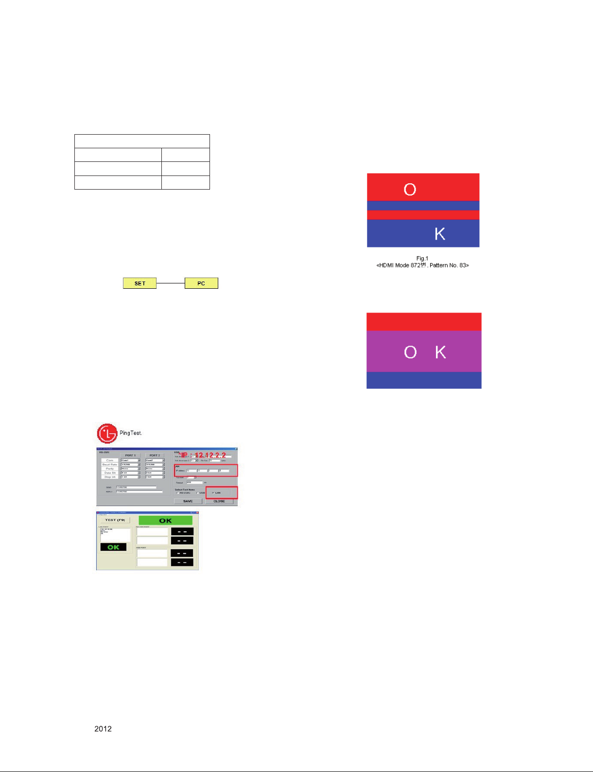
4.6. PING TEST
* In this case Network setting is on Manual Setting.
Connect : SET->LAN Port == PC->LAN Port
4.6.1. Equipment Setting
(1) Play the LAN Port Test PROGRAM.
(2) Input IP set up for an inspection to Test
* IP Number : 12.12.2.2
4.6.2. LAN PORT inspection (PING TEST)
* In this case Network setting is on Manual Setting.
(1) Play the LAN Port Test Program.
(2) connect each other LAN Port Jack.
(3) Play Test (F9) button and confirm OK Message.
(4) remove LAN CABLE
4.8. 3D function test
- Required Equipment
● Pattern Generator :
MSHG-600, MSPG-6100 [SUPPORT HDMI1.4])
MODE : HDMI mode NO. 872
Pattern No.83
(1) Please input 3D test pattern like below (HDMI mode NO.
872 , pattern No.83)
(2) When 3D OSD appear automatically, then press OK button
on ADJ Remote Controller.
(3) Check the picture. The picture must be same as below.
(Don’t have to wear 3D glasses.)
4.7. Magic Motion Remote Controller test
(1) Equipment: RF R/C for test,
(2) You must confirm the battery power of RF-R/C before test
(Recommend that change the battery per every lot)
(3) Sequence (test)
1) if you select the ‘start key(Wheel Key)’ on the controller,
you can pairing with the TV SET.
2) You can check the cursor on the TV Screen, when select
the ‘Wheel Key’ on the controller
3) You must remove the pairing with the TV Set by select
‘Mute Key’ on the controller.
5. Set Information (Serial No & Model name)
5.1. Check the serial number & Model Name
(1) Push the menu button and press red button on R/C to
enter ‘Customer Support’menu.
(2) Move to ‘signal test’ menu. And check Serial No & Model
Name Select the STATION -> Diagnostics -> To set
6. SW Download Guide.
* Before put a *.epk to USB Stick make ‘LG_DTV’ folder in
USB. Then, put *.epk file to ‘LG_DTV’ folder and Turn on TV
(1) Put the USB Stick to the USB socket
(2) Automatically detecting update file in USB Stick
* If your downloaded program version in USB Stick is Low,
it didn’t work.
But your downloaded version is High, USB data is
automatically detecting.
(3) Show the message “Copying files from memory”
(4) Updating is staring.
(5) Updating Completed, The TV will restart automatically.
After turn on TV, Please press ‘IN-STOP’ button on ADJ
Remote-control.
* IF you don’t have ADJ R/C, enter ‘Factory Reset’ in
OPTION MENU.
(6) When TV turns on, check the Updated version on Product/
Service Info. MENU.
Only for training and service purposes
- 9 -
LGE Internal Use OnlyCopyright © LG Electronics. Inc. All rights reserved.
BLOCK DIAGRAM
Only for training and service purposes
- 10 -
LGE Internal Use OnlyCopyright © LG Electronics. Inc. All rights reserved.

EXPLODED VIEW
IMPORTANT SAFETY NOTICE
Many electrical and mechanical parts in this chassis have special safety-related characteristics. These
parts are identified by in the Schematic Diagram and EXPLODED VIEW.
It is essential that these special safety parts should be replaced with the same components as
recommended in this manual to prevent X-RADIATION, Shock, Fire, or other Hazards.
Do not modify the original design without permission of manufacturer.
310
305
301
300
200
302
580
207
208
202
303
209
203
304
204
205
206
560
201
601
520
540
501
A13
A12
A9
A10
LV1
400
Only for training and service purposes
240
- 11 -
590
120
A2
900
910
LGE Internal Use OnlyCopyright © LG Electronics. Inc. All rights reserved.
+3.3V_MULTI
Copyright © 2012 LG Electronics Inc. All rights reserved.
Only for training and service purposes
LGE Internal Use Only
R108
R109 4.7K
R110 4.7K
EMMC_D[0-7]
EMMC_CLK
EMMC_CMD
EMMC_RST
R156 10K
EMMC_D[0]
EMMC_D[1]
EMMC_D[2]
EMMC_D[3]
EMMC_D[4]
EMMC_D[5]
EMMC_D[6]
EMMC_D[7]
R133
22
R172 10K
R173 10K
R174 10K
R155 10K
EMMC_D[7]
22
R157
EMMC_RST_BALL
EMMC_D[3]
EMMC_D[4]
EMMC_D[5]
+3.3V_MULTI
R175 10K
R176 10K
10K
R169
R177 10K
R178 10K
EMMC_D[6]
R179 10K
+3.3V_MULTI
C103
10uF
6.3V
C104
0.1uF
16V
C105
1uF
10V
SDIN5D2-4G-974L1
KLM2G1HE3F-B001
A3
A3
DAT0
A4
A4
DAT1
DAT1
A5
A5
DAT2
DAT2
B2
B2
DAT3
DAT3
B3
B3
DAT4
DAT4
B4
B4
DAT5
DAT5
B5
B5
DAT6
DAT6
B6
B6
DAT7
DAT7
M6
M6
CLK
CLK
M5
M5
CMD
CMD
A6
A6
NC_3
NC_3
A7
A7
NC_4
NC_4
C5
C5
NC_23
NC_23
E5
E5
NC_42
NC_42
E8
E8
NC_43
NC_43
E9
E9
NC_44
NC_44
E10
E10
NC_45
NC_45
F10
F10
NC_52
NC_52
G3
G3
NC_58
NC_58
G10
G10
NC_59
NC_59
H5
H5
NC_66
NC_66
J5
J5
NC_73
NC_73
K6
K6
NC_80
NC_80
K7
K7
NC_81
NC_81
K10
K10
NC_82
NC_82
P7
P7
NC_116
NC_116
P10
P10
NC_119
NC_119
K5
K5
RSTN
RESET
C6
C6
VDD_1
VCCQ_1
M4
M4
VDD_2
VCCQ_2
N4
N4
VDD_3
VCCQ_3
P3
P3
VDD_4
VCCQ_4
P5
P5
VDD_5
VCCQ_5
E6
E6
VDDF_1
VCC_1
F5
F5
VDDF_2
VCC_2
J10
J10
VDDF_3
VCC_3
K9
K9
VDDF_4
VCC_4
C2
C2
VDDI
VDDI
C4
E7
VSS_1
VSS_1
E7
G5
VSS_2
VSS_2
G5
H10
VSS_3
VSS_3
H10
K8
VSS_4
VSS_4
K8
C4
VSS_5
VSSQ_1
N2
N2
VSS_6
VSSQ_2
N5
N5
VSS_7
VSSQ_3
P4
P4
VSS_8
VSSQ_4
P6
P6
VSS_9
VSSQ_5
A1
A1
NC_1
NC_1
A2
A2
NC_2
NC_2
A8
A8
NC_5
NC_5
A9
A9
NC_6
NC_6
A10
A10
NC_7
NC_7
A11
A11
NC_8
NC_8
A12
A12
NC_9
NC_9
A13
A13
NC_10
NC_10
A14
A14
NC_11
NC_11
B1
B1
NC_12
NC_12
B7
B7
NC_13
NC_13
B8
B8
NC_14
NC_14
B9
B9
NC_15
NC_15
B10
B10
NC_16
NC_16
B11
B11
NC_17
NC_17
B12
B12
NC_18
NC_18
B13
B13
NC_19
NC_19
B14
B14
NC_20
NC_20
C1
C1
NC_21
NC_21
C3
C3
NC_22
NC_22
C7
C7
NC_24
NC_24
DU1
DUMMY_1
DU2
DUMMY_2
DU3
DUMMY_3
DU4
DUMMY_4
DU5
DUMMY_5
DU6
DUMMY_6
DU7
DUMMY_7
DU8
DUMMY_8
Sandisk_4GB
IC102
IC103
SS_2GBDAT0
NC_25
NC_25
NC_26
NC_26
NC_27
NC_27
NC_28
NC_28
NC_29
NC_29
NC_30
NC_30
NC_31
NC_31
NC_32
NC_32
NC_33
NC_33
NC_34
NC_34
NC_35
NC_35
NC_36
NC_36
NC_37
NC_37
NC_38
NC_38
NC_39
NC_39
NC_40
NC_40
NC_41
NC_41
NC_46
NC_46
NC_47
NC_47
NC_48
NC_48
NC_49
NC_49
NC_50
NC_50
NC_51
NC_51
NC_53
NC_53
NC_54
NC_54
NC_55
NC_55
NC_56
NC_56
NC_57
NC_57
NC_60
NC_60
NC_61
NC_61
NC_62
NC_62
NC_63
NC_63
NC_64
NC_64
NC_65
NC_65
NC_67
NC_67
NC_68
NC_68
NC_69
NC_69
NC_70
NC_70
NC_71
NC_71
NC_72
NC_72
NC_74
NC_74
NC_75
NC_75
NC_76
NC_76
NC_77
NC_77
NC_78
NC_78
NC_79
NC_79
NC_83
NC_83
NC_84
NC_84
NC_85
NC_85
NC_86
NC_86
NC_87
NC_87
NC_88
NC_88
NC_89
NC_89
NC_90
NC_90
NC_91
NC_91
NC_92
NC_92
NC_93
NC_93
NC_94
NC_94
NC_95
NC_95
NC_96
NC_96
NC_97
NC_97
NC_98
NC_98
NC_99
NC_99
NC_100
NC_100
NC_101
NC_101
NC_102
NC_102
NC_103
NC_103
NC_104
NC_104
NC_105
NC_105
NC_106
NC_106
NC_107
NC_107
NC_108
NC_108
NC_109
NC_109
NC_110
NC_110
NC_111
NC_111
NC_112
NC_112
NC_113
NC_113
NC_114
NC_114
NC_115
NC_115
NC_117
NC_117
NC_118
NC_118
NC_120
NC_120
NC_121
NC_121
NC_122
NC_122
NC_123
NC_123
DUMMY_9
DUMMY_10
DUMMY_11
DUMMY_12
DUMMY_13
DUMMY_14
DUMMY_15
DUMMY_16
/NAND_WE
NAND_D[7]
NAND_D[6] EMMC_D[6]
NAND_D[2]
NAND_D[5]
NAND_D[3]
NAND_D[4]
NAND_ALE
C8
C8
C9
C9
C10
C10
C11
C11
C12
C12
C13
C13
C14
C14
D1
D1
D2
D2
D3
D3
D4
D4
D12
D12
D13
D13
D14
D14
E1
E1
E2
E2
E3
E3
E12
E12
E13
E13
E14
E14
F1
F1
F2
F2
F3
F3
F12
F12
F13
F13
F14
F14
G1
G1
G2
G2
G12
G12
G13
G13
G14
G14
H1
H1
H2
H2
H3
H3
H12
H12
H13
H13
H14
H14
J1
J1
J2
J2
J3
J3
J12
J12
J13
J13
J14
J14
K1
K1
K2
K2
K3
K3
K12
K12
K13
K13
K14
K14
L1
L1
L2
L2
L3
L3
L12
L12
L13
L13
L14
L14
M1
M1
M2
M2
M3
M3
M7
M7
M8
M8
M9
M9
M10
M10
M11
M11
M12
M12
M13
M13
M14
M14
N1
N1
N3
N3
N6
N6
N7
N7
N8
N8
N9
N9
N10
N10
N11
N11
N12
N12
N13
N13
N14
N14
P1
P1
P2
P2
P8
P8
P9
P9
P11
P11
P12
P12
P13
P13
P14
P14
DU9
DU10
DU11
DU12
DU13
DU14
DU15
DU16
EMMC_D[5]
EMMC_D[6]
EMMC_RST_BALL
EMMC_CMD
NVRAM
OPT
R103
R100
4.7K
4.7K
OPT
R111
4.7K
+3.3V_MULTI
R125
1K
OPT
OPT
R126
1K
R1EX24256BSAS0A
A0
1
A1
2
A2
3
VSS
4
FHD
R127
1K
HD
R128
1K
R101
IC105
NVRAM_Renesas
R129
1K
R130
1K
THE SYMBOL MARK OF THIS SCHEMETIC DIAGRAM INCORPORATES
SPECIAL FEATURES IMPORTANT FOR PROTECTION FROM X-RADIATION.
FILRE AND ELECTRICAL SHOCK HAZARDS, WHEN SERVICING IF IS
ESSENTIAL THAT ONLY MANUFATURES SPECFIED PARTS BE USED FOR
THE CRITICAL COMPONENTS IN THE SYMBOL MARK OF THE SCHEMETIC.
4.7K
/NAND_RE
/NAND_CE
/NAND_RB
22
EMMC_CMD
AR100
22
1/16W
AR101
22
1/16W
EMMC_D[7]
EMMC_D[2]
EMMC_D[5]
EMMC_D[3]
EMMC_D[4]
EMMC_D[0]
EMMC_D[1]NAND_CLE
+3.3V_MULTI
C108
0.1uF
16V
VCC
8
WP
7
SCL
6
SDA
5
Model Option
R158
1K
OPT
OPT
R159
R153
1K
R160
1K
OPT
1K
R131
R132
1K
1K
R106 22
R107 22
OPT
R161
1K
R162
1K
AT24C256C-SSHL-T
A0
A1
A2
GND
T2
R163
R164
NO_T2
IC104-*1
24LC16B
VCC
C112
0.1uF
16V
A0
1
HDCP_MICRO
A1
2
A2
3
VSS
4
I2C_SCL1
I2C_SDA1
I2C_SCL5
I2C_SDA5
8
WP
7
SCL
6
SDA
5
I2C_SDA5
I2C_SCL5
I2C_SDA3
I2C_SCL3
MT5369_XTAL_IN
MT5369_XTAL_OUT
DVDD3V3_STB
PCM_A[0-14]
STRAPPINGG
+3.3V_MULTI
R104
1K
OPT
R105
1K
HDCP EEPROM
HDCP_ST
IC104
M24C16-R
NC_1
1
NC_2
2
NC_3
3
VSS
4
R112
R114
1K
1K
R113
1K
R115
1K
OPT
LED_PWM0
LED_PWM1
OPCTRL3
8
7
6
5
VCC
WC
SCL
SDA
+3.3V_MULTI
R147 4.7K
R148 22
R149 22
R122
22
OPT
R123 22
OPT
OPT
STRAPPING LED_PWM0 LED_PWM1 OPCTRL3
ICE mode + 27M + Serial boot 0 0 0
ICE mode + 27M + ROM to Nand boot 0 0 1
ICE mode + 27M + Rom to eMMC boot 0 1 0
from eMMC pins (share pins w/s NAND)
ICE mode + 27M + ROM to eMMC boot 0 1 1
from SDIO pins
FE_TS_CLK_OUT
FE_TS_VAL_OUT
FE_TS_SYNC_OUT
FE_TS_D_OUT[0-7]
I2C
+3.3V_MULTI
IC105-*1
VCC
1
8
WP
7
2
NVRAM_ATMEL
SCL
6
3
SDA
5
4
I2C_SCL5
I2C_SDA5
S
OPT
1K
R165
1K
R1661KNO_S
OPT
1K
R150
1K
R167
1K
R151
1K
R168
1K
R141 2.7K
R142
R139 2.7K
R140
R143 2.7K
R144
R102 2.7K
R121
R145 2.7K
R146
R117 2.7K
R181
MODEL_OPT_0
MODEL_OPT_1
MODEL_OPT_2
MODEL_OPT_3
MODEL_OPT_4
MODEL_OPT_5
MODEL_OPT_6
MODEL_OPT_7
MODEL_OPT_8
MODEL_OPT_9
MODEL_OPT_10
2.7K
2.7K
2.7K
2.7K
2.7K
2.7K
* I2C MAP
I2C_1 : AMP ,HDCP KEY
I2C_2 : Module
I2C_3 : MICOM
I2C_4 : S/Demod , LNB
I2C_5 : NVRAM
I2C_SCL1
I2C_6 : TUNER_MOPLL(T/C,ATV),
T2/Demod
I2C_SDA1
I2C_SCL2
I2C_SDA2
I2C_SCL3
I2C_SDA3
I2C_SCL4
I2C_SDA4
I2C_SCL5
I2C_SDA5
I2C_SCL6
I2C_SDA6
MODEL_OPT_0
MODEL_OPT_1
MODEL_OPT_2
MODEL_OPT_3
MODEL_OPT_4 3D_DEPTH
MODEL_OPT_6
MODEL_OPT_7
MODEL_OPT_8
MODEL_OPT_9
MODEL_OPT_10
MODEL OPTION 6 is just for CP Box
It should not be appiled at MP
SoC
NO_FRC
0
0
internal
FRC
0
1
LG FRC2
1
0
HIGH
FHD
OPTIC
3D_Depth_IC
DDR_Default
DDRMODEL_OPT_5
CP BOX
S Tuner
Enable
Support
Support Not Support
T2 Tuner
C2 Tuner Support Not Support
EPI
Support Not Support
external
URSA5
1
1
LOW
HD
NON_OPTIC
NO_3D_Depth_IC
DDR_768MB
Disable
Not Support
3D_SYNC_RF
M_REMOTE_ISP
S2_RESET
PCM_D[0-7]
CI_TS_D[0-7]
SC_ID
R135
R118
R119
R120
R182
R116 0
R170 0
Place the P901
OPT
R180 0
R124 0
GPIO
AP14
JTCK
AM14
JTDI
AR14
JTDO
AR15
JTMS
AN14
JTRST
PCM_D[0]
PCM_D[1]
PCM_D[2]
PCM_D[3]
PCM_D[4]
PCM_D[5]
PCM_D[6]
PCM_D[7]
CI_TS_D[0]
CI_TS_D[1]
CI_TS_D[2]
CI_TS_D[3]
CI_TS_D[4]
CI_TS_D[5]
CI_TS_D[6]
CI_TS_D[7]
TP100
TP101
TP104
AP12
AN12
AP15
AN15
AT34
AU34
AK27
AH26
AK18
AK17
AK23
AM27
AJ20
AN23
AN24
AP23
AR23
AU23
AT23
AM24
AM23
H32
F37
F36
G37
G36
G35
G34
H34
L34
L32
K33
K32
H33
L35
K36
J32
J34
K34
K35
K37
J36
J37
J35
J33
G33
H35
H31
F34
E36
N33
P32
M35
M37
M33
F35
E35
E37
N32
M34
M36
M32
L33
E33
E32
F32
A29
D31
C31
E30
E31
F31
E29
AP9
AT9
AR9
AU9
OSDA0
OSCL0
OSDA1
OSCL1
XTALI
XTALO
AVDD33_XTAL_STB
AVSS33_XTAL_STB
AVDD33_VGA_STB
AVSS33_VGA_STB
AVDD33_PLLGP
AVSS33_PLLGP
AVDD10_LDO
GPIO0
GPIO1
GPIO2
GPIO3
GPIO4
GPIO5
GPIO6
GPIO7
GPIO8
GPIO9
GPIO10
GPIO11
GPIO12
GPIO13
GPIO14
GPIO15
GPIO16
GPIO17
GPIO18
GPIO19
GPIO20
GPIO21
GPIO22
GPIO23
GPIO24
GPIO25
GPIO26
GPIO27
GPIO28
GPIO29
GPIO30
GPIO31
GPIO32
GPIO33
GPIO34
GPIO35
GPIO36
GPIO37
GPIO38
GPIO39
GPIO40
GPIO41
GPIO42
GPIO43
GPIO44
GPIO45
GPIO46
GPIO47
GPIO48
GPIO49
GPIO50
GPIO51
GPIO52
GPIO53
GPIO54
GPIO55
ADIN0_SRV
ADIN1_SRV
ADIN2_SRV
ADIN3_SRV
ADIN4_SRV
ADIN5_SRV
ADIN6_SRV
ADIN7_SRV
NVRAM, HDCP KEY
MICOM
R183 0
C101
0.1uF
DVDD3V3
C109
85C
10V
4.7uF
PCM_A[0]
PCM_A[1]
PCM_A[2]
PCM_A[3]
PCM_A[4]
PCM_A[5]
PCM_A[6]
PCM_A[7]
PCM_A[8]
PCM_A[9]
PCM_A[10]
PCM_A[11]
PCM_A[12]
PCM_A[13]
PCM_A[14]
FE_TS_D_OUT[0]
FE_TS_D_OUT[1]
FE_TS_D_OUT[2]
FE_TS_D_OUT[3]
FE_TS_D_OUT[4]
FE_TS_D_OUT[5]
FE_TS_D_OUT[6]
FE_TS_D_OUT[7]
USB_OCD2
USB_OCD1
USB_CTL2
USB_CTL1
MODEL_OPT_0
MODEL_OPT_1
MODEL_OPT_3
MODEL_OPT_7
MODEL_OPT_5
MODEL_OPT_6
NO_EU
10K
10K
10K
10K
M_REMOTE_RST
10K
TU_RST
MODEL_OPT_4
Crystal Matching Test result : 27pF -> 20pF -> 22pF
MT5369_XTAL_IN
MODEL_OPT_1AMP_RST
MODEL_OPT_5
MODEL_OPT_7
MODEL_OPT_4
IC100
LGE2112
JTAG
JTAG
JTAG
JTAG
JTAG
DEMOD_TSCLK
DEMOD_TSDATA0
DEMOD_TSDATA1
DEMOD_TSDATA2
DEMOD_TSDATA3
DEMOD_TSDATA4
DEMOD_TSDATA5
DEMOD_TSDATA6
DEMOD_TSDATA7
DEMOD_TSSYNC
DEMOD_TSVAL
PVR_TSDATA0
PVR_TSDATA1
U0TX
U0RX
U1RX
U1TX
POWE
POOE
POCE1
POCE0
PDD7
PDD6
PDD5
PDD4
PDD3
PDD2
PDD1
PDD0
PARB
PACLE
PAALE
EMMC_CLK
OPWRSB
ORESET
OIRI
FSRC_WR
STB_SCL
STB_SDA
DEMOD_RST
CI_INT
CI_TSCLK
CI_TSDATA0
CI_TSSYNC
CI_TSVAL
PVR_TSCLK
PVR_TSVAL
PVR_TSSYNC
SPI_CLK1
SPI_CLK
SPI_DATA
SPI_CLE
OPWM2
OPWM1
OPWM0
SD_D0
SD_D1
SD_D2
SD_D3
SD_CMD
SD_CLK
LDM_CS
LDM_CLK
LDM_VSYNC
LDM_DO
LDM_DI
LED_PWM1
LED_PWM0
AR18
AP18
AU16
AT16
A35
C33
B34
D33
D29
C30
D30
B31
A31
B32
A32
C32
D32
A34
C34
C29
AM20
AM22
AU21
D27
AT21
AR21
T34
T32
T36
U36
T33
T30
V33
V32
V31
V30
T35
T31
N36
T37
R35
R37
R36
R34
R32
R33
P33
P34
N37
P35
N34
N35
AU12
AT12
AR12
A37
C35
A36
B35
B36
B37
AT11
AU11
AR10
AM9
AP10
AN22
AP21
TP102
R134 4.7K
TP103
RS232_TXD
RS232_RXD
M_REMOTE_RX
M_REMOTE_TX
/NAND_WE
/NAND_RE
/NAND_CE
NAND_D[7]
NAND_D[6]
NAND_D[5]
NAND_D[4]
NAND_D[3]
NAND_D[2]
/NAND_RB
NAND_CLE
NAND_ALE
EMMC_CLK
PCM_RST
FE_TS_CLK
FE_TS_D[0]
FE_TS_D[1]
FE_TS_D[2]
FE_TS_D[3]
FE_TS_D[4]
FE_TS_D[5]
FE_TS_D[6]
FE_TS_D[7]
FE_TS_SYNC
FE_TS_VAL
/PCM_REG
/PCM_CE
CI_TS_SYNC
/PCM_WE
/PCM_OE
CI_TS_VAL
CI_TS_CLK
/PCM_IRQA
/PCM_WAIT
/CI_CD2
/CI_CD1
/PCM_IORD
/PCM_IOWR
Place the P901
LED_PWM1
LED_PWM0
SOC_RESET
I2C_SCL1
I2C_SDA1
Module
OPT
R171 0
NAND_D[2-7]
+3.3V_MULTI
R136
4.7K
OPT
R137
4.7K
OPT
AMP
SW100
JTP-1127WEM
1 2
FE_TS_D[0-7]
3D_SYNC_RF
43
5V Tolerance
AU20
OPCTRL11
AT20
OPCTRL10
AN18
OPCTRL9
AP20
OPCTRL8
AM18
OPCTRL7
AN19
OPCTRL6
AP19
OPCTRL5
AR19
OPCTRL4
AN21
OPCTRL3
AM19
OPCTRL2
AN20
OPCTRL1
AR20
OPCTRL0
X100
27MHz
1
50V
C110
22pF
TUNER_MOPLL(T/C,ATV),T2 Demod
50V
C111
22pF
I2C_SCL2
I2C_SDA2
COMP1_DET
SC/COMP2_DET
DSUB_DET
COMP1_AV1_DET
DTV_ATV_SELECT
OPCTRL3
RF_SW_CTL
I2C_SCL6
I2C_SDA6
MT5369_XTAL_OUT
Module
+1.2V_MTK_CORE
Copyright © 2012 LG Electronics Inc. All rights reserved.
Only for training and service purposes
LGE Internal Use Only
C200
0.1uF
DVDD3V3
C201
0.1uF
DVDD3V3
+1.2V_MTK_CORE DVDD3V3
DDC_SCL_2
DDC_SCL_3
DDC_SCL_4
DDC_SCL_1
DDC_SDA_2
DDC_SDA_3
DDC_SDA_4
DDC_SDA_1
5V_HDMI_2
5V_HDMI_3
5V_HDMI_4
5V_HDMI_1
WIFI_DP3
WIFI_DM3
HPD2
HPD3
HPD4
HPD1
USB_DP2
USB_DM2
USB_DP1
USB_DM1
USB_DP4
USB_DM4
C211
0.1uF
IC100
LGE2112
AA32
HDMI_CEC
AG33
HDMI_0_SCL
AE33
HDMI_1_SCL
AC33
HDMI_2_SCL
AH32
HDMI_3_SCL
AF33
HDMI_0_SDA
AD33
HDMI_1_SDA
AB33
HDMI_2_SDA
AH33
AG31
AE31
AC31
AH31
AG32
AE32
AC32
AJ32
AA24
AB24
AB29
AA29
AC29
AB30
AD30
AF31
AF32
AT13
AU13
AT14
AU14
AP13
AR13
Y24
W24
Y29
C36
C37
D36
D37
D35
D34
W35
W34
Y34
Y35
U24
V24
W30
W36
W37
HDMI_3_SDA
HDMI_0_PWR5V
HDMI_1_PWR5V
HDMI_2_PWR5V
HDMI_3_PWR5V
HDMI_0_HPD
HDMI_1_HPD
HDMI_2_HPD
HDMI_3_HPD
AVDD12_HDMI_0_RX
AVDD12_HDMI_1_RX
AVDD12_HDMI_2_RX
AVDD12_HDMI_3_RX
AVDD33_HDMI_0_RX
AVDD33_HDMI_1_RX
AVDD33_HDMI_2_RX
AVDD33_HDMI_3_RX
AVSS33_HDMI_RX_1
AVSS33_HDMI_RX_2
AVSS33_HDMI_RX_3
AVSS33_HDMI_RX_4
USB_DP_P0
USB_DM_P0
USB_DP_P1
USB_DM_P1
USB_DP_P2
USB_DM_P2
USB_DP_P3
USB_DM_P3
AVDD33_USB_P0P1
AVDD33_USB_P2P3
AVSS33_USB_P1
AVSS33_USB_P2
PCIE11_TXP
PCIE11_TXN
PCIE11_RXN
PCIE11_RXP
AVDD12_PCIE11
AVDD33_PCIE11
AVSS12_PCIE11
PCIE11_REFCKN
PCIE11_REFCKP
R2001K
R2011K
R2031K
R2041K
HDMI_0_RX_0
HDMI_0_RX_0B
HDMI_0_RX_1
HDMI_0_RX_1B
HDMI_0_RX_2
HDMI_0_RX_2B
HDMI_0_RX_C
HDMI_0_RX_CB
HDMI_1_RX_0
HDMI_1_RX_0B
HDMI_1_RX_1
HDMI_1_RX_1B
HDMI_1_RX_2
HDMI_1_RX_2B
HDMI_1_RX_C
HDMI_1_RX_CB
HDMI_2_RX_0
HDMI_2_RX_0B
HDMI_2_RX_1
HDMI_2_RX_1B
HDMI_2_RX_2
HDMI_2_RX_2B
HDMI_2_RX_C
HDMI_2_RX_CB
HDMI_3_RX_0
HDMI_3_RX_0B
HDMI_3_RX_1
HDMI_3_RX_1B
HDMI_3_RX_2
HDMI_3_RX_2B
HDMI_3_RX_C
HDMI_3_RX_CB
AVDD12_REC
AVDD33_COM
AVSS33_COM
AVSS12_REC
TXVP_0
TXVN_0
RXVN_1
RXVP_1
PHYLED1
PHYLED0
REXT
AVDD33_LD
AVSS33_LD
AG35
AG34
AG37
AG36
AF35
AF34
AH35
AH34
AE37
AE36
AD35
AD34
AC35
AC34
AE35
AE34
AB35
AB34
AA35
AA34
AA37
AA36
AC37
AC36
AK35
AK34
AJ35
AJ34
AJ37
AJ36
AJ33
AK33
AT18
AU18
AU17
AT17
AN16
AM16
AD15
AD14
AD16
AD17
AL16
AL15
AL14
D0+_HDMI2
D0-_HDMI2
D1+_HDMI2
D1-_HDMI2
D2+_HDMI2
D2-_HDMI2
CK+_HDMI2
CK-_HDMI2
D0+_HDMI3
D0-_HDMI3
D1+_HDMI3
D1-_HDMI3
D2+_HDMI3
D2-_HDMI3
CK+_HDMI3
CK-_HDMI3
D0+_HDMI4
D0-_HDMI4
D1+_HDMI4
D1-_HDMI4
D2+_HDMI4
D2-_HDMI4
CK+_HDMI4
CK-_HDMI4
D0+_HDMI1
D0-_HDMI1
D1+_HDMI1
D1-_HDMI1
D2+_HDMI1
D2-_HDMI1
CK+_HDMI1
CK-_HDMI1
EPHY_TDP
EPHY_TDN
EPHY_RDN
EPHY_RDP
R20524K
+1.2V_MTK_CORE
DVDD3V3
DIF_P
DIF_N
Close to Tuner
NO_T2_BR
C228 1uF
R214
2.2K
OPT
C2291uF
NO_T2_BR
IF_AGC
SC_CVBS_IN
COMP1_Y/AV1_CVBS
SC_B/COMP2_Y/AV2_CVBS
TU_CVBS
DVDD3V3
TU_SIF
Close to MT5395
C202
33pF
50V
NO_EU
DVDD3V3
C203
33pF
50V
NO_T2_BR
I2C_SCL4
I2C_SDA4
EU
+1.2V_MTK_CORE
MODEL_OPT_2
C245
0.1uF
SC/COMP2/AV2_R_IN
SC/COMP2/AV2_L_IN
COMP1/AV1_R_IN
COMP1/AV1_L_IN
DVDD3V3
C252
0.1uF
0 C241
R220
R221
2.2K
OPT
NO_T2_BR
R223
10K
NO_T2_BR
C232
0.047uF
25V
S/Demod , LNB
R232 100
R230 100
R229 100
R231 100
DVDD3V3
C253
0.1uF
MODEL_OPT_8
MODEL_OPT_9
MODEL_OPT_10
PCM_5V_CTL
EMMC_RST
C254
0.1uF
PC_R_IN
PC_L_IN
C242
0.01uF
50V
0.01uF
Close to MT5395
51
R225
NO_T2_BR
51
R233
+1.2V_MTK_CORE
Close to MT5395
C239 0.047uF
C227 0.047uF
C226 0.047uF
C238 0.047uF
C225 1uF
R235
C243
10V
F27
E27
F30
F29
B27
A27
B28
A28
C28
D28
E28
F28
B29
AG6
AJ6
AF6
AE6
AH7
AJ5
AG5
AF5
AE5
AH5
AG7
24K
1%
AU37
AU35
AT35
AT37
AU36
AP34
AT36
AR37
AR33
AP32
AR36
AP37
AR35
AP36
AL31
1uF
AJ28
AJ27
AN28
AU32
AT32
AD22
AL27
AM28
AJ26
U35
U34
TP207
AP31
TP201
AN30
TP202
V35
V34
AP28
AR29
AT30
EU
AR30
AR31
AN29
NO_EU
AP30
AK24
AK25
AL25
AM26
IC100
LGE2112
TCON0
TCON1
TCON2
TCON3
TCON4
TCON5
TCON6
TCON7
TCON8
TCON9
TCON10
TCON11
TCON12
AVDD12_LVDS_1
AVDD12_LVDS_2
AVDD12_VPLL
AVDD33_LVDSB
AVDD33_LVDSA
AVSS12_LVDS_2
AVSS12_LVDS_1
AVSS12_VPLL
AVSS33_LVDSB
AVSS33_LVDSA
REXT_VPLL
AIN0_R_AADC
AIN0_L_AADC
AIN1_R_AADC
AIN1_L_AADC
AIN2_R_AADC
AIN2_L_AADC
AIN3_R_AADC
AIN3_L_AADC
AIN4_R_AADC
AIN4_L_AADC
AIN5_R_AADC
AIN5_L_AADC
AIN6_R_AADC
AIN6_L_AADC
AVDD33_AADC
AVSS33_AADC
VMID_AADC
MPXP
ADCINP_DEMOD
ADCINN_DEMOD
AVDD33_DEMOD
AVDD12_DEMOD
AVSS33_DEMOD
AVSS12_DEMOD
IF_AGC
RF_AGC
LOUTN
LOUTP
OSCL2
OSDA2
SC0
SY0
CVBS3P
CVBS2P
CVBS1P
CVBS0P
CVBS_COM
AVDD33_CVBS_1
AVDD33_CVBS_2
AVSS33_CVBS_1
AVSS33_CVBS_2
AO3N
AO3P
AO4N
AO4P
AOCLKN
AOCLKP
AO2N
AO2P
AO1N
AO1P
AO0N
AO0P
AE4N
AE4P
AE3N
AE3P
AECLKN
AECLKP
AE2N
AE2P
AE1N
AE1P
AE0N
AE0P
BO4N
BO4P
BO3N
BO3P
BOCLKN
BOCLKP
BO2N
BO2P
BO1N
BO1P
BO0N
BO0P
BE4N
BE4P
BE3N
BE3P
BECLKN
BECLKP
BE2N
BE2P
BE1N
BE1P
BE0N
BE0P
AR0_ADAC
AL0_ADAC
AR1_ADAC
AL1_ADAC
AR2_ADAC
AL2_ADAC
AR3_ADAC
AL3_ADAC
AVDD33_DAC
AVDD33_DAC1
AVSS33_DAC
AVSS33_DAC1
ALIN
ASPDIF0
ASPDIF1
AOBCK
AOLRCK
AOMCLK
AOSDATA4
AOSDATA3
AOSDATA2
AOSDATA1
AOSDATA0
HSYNC
VSYNC
VGA_SDA
VGA_SCL
COM1
PB1P
PR1P
SOY1
COM0
PB0P
PR0P
SOY0
VDACX_OUT
VDACY_OUT
AVDD33_VDAC_BG
AVDD33_VDAC
AVDD12_RGB
AVSS33_VDAC_BG
AVSS12_RGB
AVSS33_VDAC
AG3
AG4
AG1
AG2
AF3
AF4
AE3
AE4
AE1
AE2
AD1
AD2
AL3
AL4
AL1
AL2
AK3
AK4
AJ3
AJ4
AJ1
AJ2
AH3
AH4
AT2
AU2
AT1
AU1
AR1
AR2
AP1
AP2
AN1
AN2
AM3
AM4
AT6
AU6
AP6
AR6
AP5
AR5
AT4
AU4
AP4
AR4
AP3
AR3
AN35
AN34
AM32
EU
AM34
EU
AM37
AM33
AM36
AM35
AG30
AF30
AK30
AE30
Y33
AR16
Y32
AR11
AP11
AM12
AM10
TP203
AM11
TP204
AN11
TP205
AN10
TP206
AN9
AN25
AM25
AR25
RP
AR24
GP
AU24
BP
AP24
COM
AT24
SOG
AR22
AP22
AT26
AR26
AP26
AU26
Y1P
AP25
AU28
AT28
AR28
AP27
Y0P
AR27
AU30
TP200
AP29
AD20
AD21
AD19
AJ22
AJ21
AL24
RXD0+
RXD0RXD1+
RXD1RXD2+
RXD2RXDCK+
RXDCKRXD3+
RXD3RXD4+
RXD4-
RXC0+
RXC0RXC1+
RXC1RXC2+
RXC2RXCCK+
RXCCKRXC3+
RXC3RXC4+
RXC4-
RXB0+
RXB0RXB1+
RXB1RXB2+
RXB2RXBCK+
RXBCKRXB3+
RXB3RXB4+
RXB4-
RXA0+
RXA0RXA1+
RXA1RXA2+
RXA2RXACK+
RXACKRXA3+
RXA3RXA4+
RXA4-
R23615K
R23715K
C204
330pF
50V
EU
Don’t use as GPIO
C2050.01uF
C2070.01uF
C2090.01uF
C2101500pF
C2230.01uF
C2190.01uF
C2210.01uF
C2241500pF
C2480.01uF R240100
C2120.01uF
C2140.01uF
EU
C2571500pF
SC_CVBS_OUT
NO_EU
C206
330pF
50V
EU
DAC_3V3
C250
0.1uF
R208100
R210100
R212100
R238100C2460.01uF
RGB_DDC_SDA
RGB_DDC_SCL
R239100C2470.01uF
R226100
R222100
R224100
R219100C2160.01uF
R215100
R217100
R2060
SC_ROUT
SC_LOUT
SPDIF_OUT
ARC
AUD_SCK
AUD_LRCK
AUD_MCLK
AUD_LRCH
DSUB_HSYNC
DSUB_VSYNC
DSUB_R
DSUB_G
DSUB_B
SC_G/COMP2_Pb
SC_R/COMP2_Pr
SC_B/COMP2_Y/AV2_CVBS
COMP1_Pb
COMP1_Pr
COMP1_Y/AV1_CVBS
SC_FB
DVDD3V3
+1.2V_MTK_CORE
JACK SIDE PLACE
R589
0
1/16W
5%
P200
TF05-51S
HD
52
LVDS
RXD4+
RXD4RXD3+
RXD3-
RXDCK+
RXDCK-
RXD2+
RXD2RXD1+
RXD1RXD0+
RXD0-
RXC4+
RXC4RXC3+
RXC3-
RXCCK+
RXCCK-
RXC2+
RXC2RXC1+
RXC1RXC0+
RXC0-
RXB4+
RXB4RXB3+
RXB3-
RXBCK+
RXBCK-
RXB2+
RXB2RXB1+
RXB1RXB0+
RXB0-
RXA4+
RXA4RXA3+
RXA3-
RXACK+
RXACK-
RXA2+
RXA2RXA1+
RXA1RXA0+
RXA0-
DISP_EN
I2C_SDA2
I2C_SCL2
+3.3V_MULTI
4.7K
R245
R202
2K
+3.3V_MULTI
R248
4.7K
R244
4.7K
A2CA1
D200
MMBD6100
+3.3V_MULTI
B
R211
47K
R249
4.7K
ROM_DW_DA
ROM_DW_CK
R213
4.7K
C
Q200
MMBT3904(NXP)
E
LD200
LTST-C150KGKT
P201
104060-8017
FHD
1
2
3
4
5
6
7
8
9
10
11
12
13
14
15
16
17
18
19
20
21
22
23
24
25
26
27
28
29
30
31
32
33
34
35
36
37
38
39
40
41
42
43
44
45
46
47
48
49
50
51
RXB4+
RXB4RXB3+
RXB3-
RXBCK+
RXBCK-
RXB2+
RXB2RXB1+
RXB1RXB0+
RXB0-
RXA4+
RXA4RXA3+
RXA3-
RXACK+
RXACK-
RXA2+
RXA2RXA1+
RXA1RXA0+
RXA0-
1
2
3
4
5
6
7
8
9
10
11
12
13
14
15
16
17
18
19
20
21
22
23
24
25
26
27
28
29
30
31
32
33
34
35
36
37
38
39
40
41
42
43
44
45
46
47
48
49
50
51
52
53
54
55
56
57
58
59
60
61
62
63
64
65
66
67
68
69
70
71
72
73
74
75
76
77
78
79
80
81
R250 0
R242100
R207
22
R209
22
R243
27K
OPT
THE SYMBOL MARK OF THIS SCHEMETIC DIAGRAM INCORPORATES
SPECIAL FEATURES IMPORTANT FOR PROTECTION FROM X-RADIATION.
FILRE AND ELECTRICAL SHOCK HAZARDS, WHEN SERVICING IF IS
ESSENTIAL THAT ONLY MANUFATURES SPECFIED PARTS BE USED FOR
THE CRITICAL COMPONENTS IN THE SYMBOL MARK OF THE SCHEMETIC.
CORE 1.2V : 6100mA
Copyright © 2012 LG Electronics Inc. All rights reserved.
Only for training and service purposes
LGE Internal Use Only
MULTI 3.3V : XXXXmA
+1.2V_MTK_CORE
6.3V
C321
22uF
6.3V
C317
10uF
C319
10uF
6.3V
C324
22uF
6.3V
C322
0.1uF
C328
0.1uF
C325
0.1uF
C329
0.1uF
C340
0.1uF
C333
0.1uF
L300
BLM18PG121SN1D
L310
BLM18PG121SN1D
C316
0.1uF
AZ1117BH-ADJTRE1
INPUT
3
OUTPUT
DVDD3V3
60mA5600mA
L302
6.3V
C327
10uF
IC300
ADJ/GND
1
2
R1
R300
*V0=1.25(1+R2/R1)
=3.37
6.3V
C300
10uF
AVDD3V3_MEMPLL
DVDD3V3_STB
1%
330
C335
0.1uF
R2
R302
560
OPT
1%
C307
0.1uF
C310
0.1uF
C311
0.1uF
R303
AA15
AB15
AA16
AB16
AA17
AB17
R2
R3
J4
R4
Y4
F5
J5
R5
Y5
W5
L7
M7
R7
AA5
AB5
K7
U7
W7
E9
E8
F9
G14
J6
R15
T15
U15
V15
W15
Y15
H11
R16
T16
U16
V16
W16
Y16
R17
T17
U17
V17
Y17
T18
V18
Y18
T19
V19
Y19
W17
R18
AB6
H19
H22
J11
J12
J22
VCCK_43
VCCK_45
VCCK_47
VCCK_42
VCCK_44
VCCK_46
VCCK_48
VCCK_37
VCCK_39
VCCK_41
VCCK_38
VCCK_40
VCCK_1
VCCK_9
VCCK_11
VCCK_13
VCCK_14
VCCK_16
VCCK_18
VCCK_20
VCCK_22
VCCK_23
VCCK_28
VCCK_2
VCCK_24
VCCK_3
VCCK_25
VCCK_15
VCCK_17
VCCK_19
VCCK_21
DVSS_51
DVSS_52
DVSS_37
DVSS_53
DVSS_107
DVSS_20
DVSS_38
DVSS_54
DVSS_108
DVSS_95
DVSS_44
DVSS_46
DVSS_56
DVSS_120
DVSS_130
DVSS_43
DVSS_77
DVSS_97
DVSS_13
DVSS_12
DVSS_22
DVSS_28
DVSS_39
DVSS_57
DVSS_68
DVSS_78
DVSS_87
DVSS_99
DVSS_112
DVSS_122
DVSS_132
DVSS_34
DVSS_58
DVSS_69
DVSS_79
DVSS_88
DVSS_100
DVSS_113
DVSS_123
DVSS_133
DVSS_59
DVSS_70
DVSS_80
DVSS_89
DVSS_114
DVSS_71
DVSS_90
DVSS_115
DVSS_72
DVSS_91
DVSS_116
DVSS_101
DVSS_124
DVSS_134
DVSS_60
DVSS_131
DVSS_35
DVSS_36
DVSS_40
DVSS_41
DVSS_42
IC100
LGE2112
IC100
LGE2112
VCCK_31
VCCK_32
VCCK_36
VCCK_8
VCCK_10
VCCK_12
VCCK_33
VCCK_30
VCCK_7
VCCK_29
VCCK_6
VCCK_27
VCCK_5
VCCK_26
VCCK_4
VCCK_34
VCCK_35
VCC3IO_B_4
VCC3IO_B_2
VCC3IO_B_1
VCC3IO_B_3
VCC3IO_A_5
VCC3IO_A_7
VCC3IO_A_6
VCC3IO_A_8
VCC3IO_A_3
VCC3IO_A_4
VCC3IO_A_2
VCC3IO_A_1
DVSS_104
DVSS_117
DVSS_127
DVSS_137
DVSS_105
DVSS_118
DVSS_128
DVSS_138
DVSS_106
DVSS_119
DVSS_129
DVSS_139
DVSS_140
DVSS_109
DVSS_136
DVSS_126
DVSS_103
DVSS_110
DVSS_135
DVSS_125
DVSS_102
DVSS_121
DVSS_111
DVSS_55
DVSS_62
DVSS_73
DVSS_83
DVSS_92
DVSS_29
DVSS_63
DVSS_74
DVSS_84
DVSS_93
DVSS_64
DVSS_75
DVSS_85
DVSS_94
DVSS_65
DVSS_76
DVSS_86
DVSS_96
DVSS_30
DVSS_27
DVSS_17
DVSS_25
DVSS_45
DVSS_66
DVSS_7
DVSS_14
DVSS_8
DVSS_18
DVSS_26
DVSS_33
DVSS_49
DVSS_82
DVSS_61
DVSS_81
DVSS_47
DVSS_67
DVSS_98
DVSS_11
DVSS_21
C313
0.1uF
0.1uF
DAC_3V3
1
C354
10uF
6.3V
0.1uF
C315
0.1uF
C308
0.1uF
OPT
C312
C306
+1.2V_MTK_CORE
AA14
AB14
AC14
AC19
AC15
AC16
AA23
AR7
AT7
AU7
AP8
AR8
AT8
AU8
AM7
AN7
AP7
AM8
AN8
P14
R14
T14
U14
V14
W14
Y14
P15
P16
V23
W23
Y23
AC22
AC23
AD24
P23
R24
T24
AC24
AC21
P20
AC20
P19
AC18
P18
AC17
P17
AD18
AD23
AL9
AK10
AK9
AK11
H29
J29
H30
J30
G31
G32
F33
E34
R6
R20
T20
U20
V20
W20
Y20
AA20
AB20
G16
R21
T21
U21
V21
W21
Y21
AA21
AB21
R22
T22
U22
V22
W22
Y22
AA22
AB22
R23
T23
U23
AB23
W6
G17
F25
Y6
E21
F21
L8
T7
D11
E11
D12
E22
F22
G25
AB19
AA19
P22
W19
U19
R19
Y7
AB18
AA18
W18
U18
AA7
N22
T8
W8
Y8
E7
F8
+1.2V_MTK_CORE
DVDD3V3
INNER CAP
C336
0.1uF
P_+5V
+3.3V_MULTI
C305
10uF
6.3V
C352
10uF
10V
BLM18PG121SN1D
OPT
OPT
C304
0.1uF
INNER CAP
C301
0.1uF
On the Main chip
OPT
C309
0.1uF
INNER CAP
C303
0.1uF
C343
0.1uF
OPT
C337
C341
0.1uF
0.1uF
C302
0.1uF
BOTTOM PCB FOR REWORKING
C350
C347
0.1uF
0.1uF
THE SYMBOL MARK OF THIS SCHEMETIC DIAGRAM INCORPORATES
SPECIAL FEATURES IMPORTANT FOR PROTECTION FROM X-RADIATION.
FILRE AND ELECTRICAL SHOCK HAZARDS, WHEN SERVICING IF IS
ESSENTIAL THAT ONLY MANUFATURES SPECFIED PARTS BE USED FOR
THE CRITICAL COMPONENTS IN THE SYMBOL MARK OF THE SCHEMETIC.
B_RVREF5
Copyright © 2012 LG Electronics Inc. All rights reserved.
Only for training and service purposes
LGE Internal Use Only
R409
ARA[14]
B_RVREF6
R408
BRA[14]
A_RVREF4
A_RVREF1
+1.5V_DDR
+1.5V_DDR
M8
H1
1%
240
L8
B2
D9
G7
K2
K8
N1
N9
R1
R9
A1
A8
C1
C9
D2
E9
F1
H2
H9
J1
J9
L1
L9
T7
A9
B3
E1
G8
J2
J8
M1
M9
P1
P9
T1
T9
B1
B9
D1
D8
E2
E8
F9
G1
G9
M8
H1
1%
240
L8
B2
D9
G7
K2
K8
N1
N9
R1
R9
A1
A8
C1
C9
D2
E9
F1
H2
H9
J1
J9
L1
L9
T7
A9
B3
E1
G8
J2
J8
M1
M9
P1
P9
T1
T9
B1
B9
D1
D8
E2
E8
F9
G1
G9
IC401
H5TQ2G63BFR-PBC
HYNIX
VREFCA
VREFDQ
ZQ
VDD_1
VDD_2
VDD_3
VDD_4
VDD_5
VDD_6
VDD_7
VDD_8
VDD_9
VDDQ_1
VDDQ_2
VDDQ_3
VDDQ_4
VDDQ_5
VDDQ_6
VDDQ_7
VDDQ_8
VDDQ_9
NC_1
NC_2
NC_3
NC_4
NC_6
VSS_1
VSS_2
VSS_3
VSS_4
VSS_5
VSS_6
VSS_7
VSS_8
VSS_9
VSS_10
VSS_11
VSS_12
VSSQ_1
VSSQ_2
VSSQ_3
VSSQ_4
VSSQ_5
VSSQ_6
VSSQ_7
VSSQ_8
VSSQ_9
IC400
H5TQ2G63BFR-PBC
HYNIX
VREFCA
VREFDQ
ZQ
VDD_1
VDD_2
VDD_3
VDD_4
VDD_5
VDD_6
VDD_7
VDD_8
VDD_9
VDDQ_1
VDDQ_2
VDDQ_3
VDDQ_4
VDDQ_5
VDDQ_6
VDDQ_7
VDDQ_8
VDDQ_9
NC_1
NC_2
NC_3
NC_4
NC_6
VSS_1
VSS_2
VSS_3
VSS_4
VSS_5
VSS_6
VSS_7
VSS_8
VSS_9
VSS_10
VSS_11
VSS_12
VSSQ_1
VSSQ_2
VSSQ_3
VSSQ_4
VSSQ_5
VSSQ_6
VSSQ_7
VSSQ_8
VSSQ_9
A10/AP
A12/BC
RESET
DQSL
DQSL
DQSU
DQSU
DQL0
DQL1
DQL2
DQL3
DQL4
DQL5
DQL6
DQL7
DQU0
DQU1
DQU2
DQU3
DQU4
DQU5
DQU6
DQU7
A10/AP
A12/BC
RESET
DQSL
DQSL
DQSU
DQSU
DQL0
DQL1
DQL2
DQL3
DQL4
DQL5
DQL6
DQL7
DQU0
DQU1
DQU2
DQU3
DQU4
DQU5
DQU6
DQU7
ARBA0
ARBA1
ARBA2
ARCKE
/ARCS
ARODT
/ARRAS
/ARCAS
/ARWE
ARREST
ARDQS0
/ARDQS0
ARDQS1
/ARDQS1
ARDQM0
ARDQM1
BRBA0
BRBA1
BRBA2
BRCKE
/BRCS
BRODT
/BRRAS
/BRCAS
/BRWE
BRREST
BRDQS0
/BRDQS0
BRDQS1
/BRDQS1
BRDQM0
BRDQM1
ARA[0-13]
BRA[0-13]
R421
100
5%
R422
100
5%
ARDQ[8-15]
BRDQ[8-15]
ARA[0]
N3
A0
ARA[1]
P7
A1
ARA[2]
P3
A2
ARA[3]
N2
A3
ARA[4]
P8
A4
ARA[5]
P2
A5
ARA[6]
R8
A6
ARA[7]
R2
A7
ARA[8]
T8
A8
ARA[9]
R3
A9
ARA[10]
L7
ARA[11]
R7
A11
ARA[12]
N7
ARA[13]
T3
A13
M7
A15
M2
BA0
N8
BA1
M3
BA2
J7
CK
K7
CK
K9
CKE
L2
CS
K1
ODT
J3
RAS
K3
CAS
L3
WE
T2
F3
G3
C7
B7
E7
DML
D3
DMU
E3
F7
F2
F8
H3
H8
G2
H7
D7
C3
C8
C2
A7
A2
B8
A3
BRA[0]
N3
A0
BRA[1]
P7
A1
BRA[2]
P3
A2
BRA[3]
N2
A3
BRA[4]
P8
A4
BRA[5]
P2
A5
BRA[6]
R8
A6
BRA[7]
R2
A7
BRA[8]
T8
A8
BRA[9]
R3
A9
BRA[10]
L7
BRA[11]
R7
A11
BRA[12]
N7
BRA[13]
T3
A13
M7
A15
M2
BA0
N8
BA1
M3
BA2
J7
CK
K7
CK
K9
CKE
L2
CS
K1
ODT
J3
RAS
K3
CAS
L3
WE
T2
F3
G3
C7
B7
E7
DML
D3
DMU
E3
F7
F2
F8
H3
H8
G2
H7
D7
C3
C8
C2
A7
A2
B8
A3
A_RVREF1
A_RVREF4
A_RVREF2
A_RVREF3
ARDQ[0-7]
BRDQ[0-7]
ARCLK0
/ARCLK0
B_RVREF5
B_RVREF6
BRCLK0
/BRCLK0
B_RVREF7
B_RVREF8
+1.5V_DDR
+1.5V_DDR
+1.5V_DDR
+1.5V_DDR
+1.5V_DDR
+1.5V_DDR
+1.5V_DDR
+1.5V_DDR
R400
1K
1%
R401
1K
1%
R402
1K
1%
R403
1K
1%
R432
1K
1%
R433
1K
1%
R430
1K
1%
R431
1K
1%
R404
1K
1%
R405
1K
1%
R406
1K
1%
R407
1K
1%
R428
1K
1%
R429
1K
1%
R426
1K
1%
R427
1K
1%
C402
0.01uF
C403
0.01uF
C404
0.01uF
C405
0.01uF
C461
0.01uF
C462
0.01uF
C459
0.01uF
C460
0.01uF
C408
0.01uF
C409
0.01uF
C410
0.01uF
C411
0.01uF
C457
0.01uF
C458
0.01uF
C455
0.01uF
C456
0.01uF
ARCLK1
/ARCLK1
ARDQ[16-23]
ARDQ[24-31]
BRCLK1
R423
/BRCLK1
BRDQ[16-23]
BRDQ[24-31]
THE SYMBOL MARK OF THIS SCHEMETIC DIAGRAM INCORPORATES
SPECIAL FEATURES IMPORTANT FOR PROTECTION FROM X-RADIATION.
FILRE AND ELECTRICAL SHOCK HAZARDS, WHEN SERVICING IF IS
ESSENTIAL THAT ONLY MANUFATURES SPECFIED PARTS BE USED FOR
THE CRITICAL COMPONENTS IN THE SYMBOL MARK OF THE SCHEMETIC.
100
R420
100
5%
5%
ARA[0-13]
BRA[0-13]
ARBA0
ARBA1
ARBA2
ARCKE
/ARCS
ARODT
/ARRAS
/ARCAS
/ARWE
ARREST
ARDQS2
/ARDQS2
ARDQS3
/ARDQS3
ARDQM2
ARDQM3
ARDQ[16]
ARDQ[17]
ARDQ[18]
ARDQ[19]
ARDQ[20]
ARDQ[21]
ARDQ[22]
ARDQ[23]
ARDQ[24]
ARDQ[25]
ARDQ[26]
ARDQ[27]
ARDQ[28]
ARDQ[29]
ARDQ[30]
ARDQ[31]
BRBA0
BRBA1
BRBA2
BRCKE
/BRCS
BRODT
/BRRAS
/BRCAS
/BRWE
BRREST
BRDQS2
/BRDQS2
BRDQS3
/BRDQS3
BRDQM2
BRDQM3
BRDQ[16]
BRDQ[17]
BRDQ[18]
BRDQ[19]
BRDQ[20]
BRDQ[21]
BRDQ[22]
BRDQ[23]
BRDQ[24]
BRDQ[25]
BRDQ[26]
BRDQ[27]
BRDQ[28]
BRDQ[29]
BRDQ[30]
BRDQ[31]
ARA[0]
ARA[1]
ARA[2]
ARA[3]
ARA[4]
ARA[5]
ARA[6]
ARA[7]
ARA[8]
ARA[9]
ARA[10]
ARA[11]
ARA[12]
ARA[13]
BRA[0]
BRA[1]
BRA[2]
BRA[3]
BRA[4]
BRA[5]
BRA[6]
BRA[7]
BRA[8]
BRA[9]
BRA[10]
BRA[11]
BRA[12]
BRA[13]
IC402
H5TQ2G63BFR-PBC
N3
P7
P3
N2
P8
P2
R8
R2
T8
R3
L7
R7
N7
T3
M7
M2
N8
M3
J7
K7
K9
L2
K1
J3
K3
L3
T2
F3
G3
C7
B7
E7
D3
E3
F7
F2
F8
H3
H8
G2
H7
D7
C3
C8
C2
A7
A2
B8
A3
N3
P7
P3
N2
P8
P2
R8
R2
T8
R3
L7
R7
N7
T3
M7
M2
N8
M3
J7
K7
K9
L2
K1
J3
K3
L3
T2
F3
G3
C7
B7
E7
D3
E3
F7
F2
F8
H3
H8
G2
H7
D7
C3
C8
C2
A7
A2
B8
A3
HYNIX
A0
A1
A2
A3
A4
A5
A6
A7
A8
A9
A10/AP
A11
A12/BC
A13
A15
BA0
BA1
BA2
CK
CK
CKE
CS
ODT
RAS
CAS
WE
RESET
DQSL
DQSL
DQSU
DQSU
DML
DMU
DQL0
DQL1
DQL2
DQL3
DQL4
DQL5
DQL6
DQL7
DQU0
DQU1
DQU2
DQU3
DQU4
DQU5
DQU6
DQU7
IC403
H5TQ2G63BFR-PBC
HYNIX
A0
A1
A2
A3
A4
A5
A6
A7
A8
A9
A10/AP
A11
A12/BC
A13
A15
BA0
BA1
BA2
CK
CK
CKE
CS
ODT
RAS
CAS
WE
RESET
DQSL
DQSL
DQSU
DQSU
DML
DMU
DQL0
DQL1
DQL2
DQL3
DQL4
DQL5
DQL6
DQL7
DQU0
DQU1
DQU2
DQU3
DQU4
DQU5
DQU6
DQU7
VREFCA
VREFDQ
VDD_1
VDD_2
VDD_3
VDD_4
VDD_5
VDD_6
VDD_7
VDD_8
VDD_9
VDDQ_1
VDDQ_2
VDDQ_3
VDDQ_4
VDDQ_5
VDDQ_6
VDDQ_7
VDDQ_8
VDDQ_9
NC_1
NC_2
NC_3
NC_4
NC_6
VSS_1
VSS_2
VSS_3
VSS_4
VSS_5
VSS_6
VSS_7
VSS_8
VSS_9
VSS_10
VSS_11
VSS_12
VSSQ_1
VSSQ_2
VSSQ_3
VSSQ_4
VSSQ_5
VSSQ_6
VSSQ_7
VSSQ_8
VSSQ_9
VREFCA
VREFDQ
VDD_1
VDD_2
VDD_3
VDD_4
VDD_5
VDD_6
VDD_7
VDD_8
VDD_9
VDDQ_1
VDDQ_2
VDDQ_3
VDDQ_4
VDDQ_5
VDDQ_6
VDDQ_7
VDDQ_8
VDDQ_9
NC_1
NC_2
NC_3
NC_4
NC_6
VSS_1
VSS_2
VSS_3
VSS_4
VSS_5
VSS_6
VSS_7
VSS_8
VSS_9
VSS_10
VSS_11
VSS_12
VSSQ_1
VSSQ_2
VSSQ_3
VSSQ_4
VSSQ_5
VSSQ_6
VSSQ_7
VSSQ_8
VSSQ_9
IC100
A_RVREF2
M8
A_RVREF3
H1
L8
ZQ
+1.5V_DDR
B2
D9
G7
K2
K8
N1
N9
R1
R9
A1
A8
C1
C9
D2
E9
F1
H2
H9
J1
J9
L1
L9
T7
A9
B3
E1
G8
J2
J8
M1
M9
P1
P9
T1
T9
B1
B9
D1
D8
E2
E8
F9
G1
G9
M8
H1
L8
ZQ
+1.5V_DDR
B2
D9
G7
K2
K8
N1
N9
R1
R9
A1
A8
C1
C9
D2
E9
F1
H2
H9
J1
J9
L1
L9
T7
A9
B3
E1
G8
J2
J8
M1
M9
P1
P9
T1
T9
B1
B9
D1
D8
E2
E8
F9
G1
G9
R424
R425
1%
240
ARA[14]
1%
240
BRA[14]
B_RVREF8
B_RVREF7
+1.5V_DDR
+1.5V_DDR
+1.5V_DDR
+1.5V_DDR
C401
0.1uF
C400
0.1uF
C467
0.1uF
C468
0.1uF
C407
0.1uF
C406
0.1uF
C474
0.1uF
K4B2G1646C-HCK0
SS
N3
A0
P7
A1
P3
A2
N2
A3
P8
A4
P2
A5
R8
A6
R2
A7
T8
A8
R3
A9
L7
A10/AP
R7
A11
N7
A12/BC
T3
A13
M7
NC_5
M2
BA0
N8
BA1
M3
BA2
J7
CK
K7
CK
K9
CKE
L2
CS
K1
ODT
J3
RAS
K3
CAS
L3
WE
T2
RESET
F3
DQSL
G3
DQSL
C7
DQSU
B7
DQSU
E7
DML
D3
DMU
E3
DQL0
F7
DQL1
F2
DQL2
F8
DQL3
H3
DQL4
H8
DQL5
G2
DQL6
H7
DQL7
D7
DQU0
C3
DQU1
C8
DQU2
C2
DQU3
A7
DQU4
A2
DQU5
B8
DQU6
A3
DQU7
C473
0.1uF
IC400-*1
INNER CAP
INNER CAP
C420
C413
1uF
C415
1uF
C417
1uF
C419
0.1uF
C423
0.1uF
0.1uF
On the Main chip
+1.5V_DDR
C412
0.1uF
C414
0.1uF
C416
0.1uF
C418
0.1uF
C421
0.1uF
OPT
OPT
C424
0.1uF
OPT
C422
0.1uF
RVREF_A
RVREF_B
TP1
TP2
BOTTOM PCB FOR REWORKING
ARCKE
ARCLK1
/ARCLK1
ARCLK0
/ARCLK0
ARODT
/ARRAS
/ARCAS
/ARCS
/ARWE
ARREST
ARBA0
ARBA1
ARBA2
ARA[14]
ARA[13]
ARA[12]
ARA[11]
ARA[10]
ARA[9]
ARA[8]
ARA[7]
ARA[6]
BRCLK0
BRCLK1
BRCKE
BRODT
/BRRAS
/BRCAS
/BRCS
BRBA0
BRBA1
BRBA2
/BRWE
BRA[14]
BRA[13]
BRA[12]
BRA[11]
BRA[10]
BRA[9]
BRA[8]
BRA[7]
BRA[6]
BRA[5]
BRA[4]
BRA[3]
BRA[2]
BRA[1]
BRA[0]
ARA[5]
ARA[4]
ARA[3]
ARA[2]
ARA[1]
ARA[0]
+1.5V_DDR
IC403-*1
IC401-*1
K4B2G1646C-HCK0
SS
M8
VREFCA
H1
VREFDQ
L8
ZQ
B2
VDD_1
D9
VDD_2
G7
VDD_3
K2
VDD_4
K8
VDD_5
N1
VDD_6
N9
VDD_7
R1
VDD_8
R9
VDD_9
A1
VDDQ_1
A8
VDDQ_2
C1
VDDQ_3
C9
VDDQ_4
D2
VDDQ_5
E9
VDDQ_6
F1
VDDQ_7
H2
VDDQ_8
H9
VDDQ_9
J1
NC_1
J9
NC_2
L1
NC_3
L9
NC_4
T7
NC_6
A9
VSS_1
B3
VSS_2
E1
VSS_3
G8
VSS_4
J2
VSS_5
J8
VSS_6
M1
VSS_7
M9
VSS_8
P1
VSS_9
P9
VSS_10
T1
VSS_11
T9
VSS_12
B1
VSSQ_1
B9
VSSQ_2
D1
VSSQ_3
D8
VSSQ_4
E2
VSSQ_5
E8
VSSQ_6
F9
VSSQ_7
G1
VSSQ_8
G9
VSSQ_9
N3
M8
A0
VREFCA
P7
A1
P3
A2
N2
H1
A3
VREFDQ
P8
A4
P2
A5
R8
L8
A6
ZQ
R2
A7
T8
A8
B2
R3
VDD_1
A9
D9
L7
VDD_2
A10/AP
G7
R7
VDD_3
A11
N7
K2
VDD_4
A12/BC
T3
K8
A13
VDD_5
N1
VDD_6
M7
N9
NC_5
VDD_7
R1
VDD_8
M2
R9
BA0
VDD_9
N8
BA1
M3
BA2
A1
VDDQ_1
J7
A8
CK
VDDQ_2
K7
C1
CK
VDDQ_3
K9
C9
CKE
VDDQ_4
D2
VDDQ_5
L2
E9
CS
VDDQ_6
K1
F1
ODT
VDDQ_7
J3
H2
RAS
VDDQ_8
K3
H9
CAS
VDDQ_9
L3
WE
J1
NC_1
T2
J9
RESET
NC_2
L1
NC_3
L9
NC_4
F3
T7
DQSL
NC_6
G3
DQSL
C7
A9
DQSU
VSS_1
B7
B3
DQSU
VSS_2
E1
VSS_3
E7
G8
DML
VSS_4
D3
J2
DMU
VSS_5
J8
VSS_6
E3
M1
DQL0
VSS_7
F7
M9
DQL1
VSS_8
F2
P1
DQL2
VSS_9
F8
P9
DQL3
VSS_10
H3
T1
DQL4
VSS_11
H8
T9
DQL5
VSS_12
G2
DQL6
H7
DQL7
B1
VSSQ_1
D7
B9
DQU0
VSSQ_2
C3
D1
DQU1
VSSQ_3
C8
D8
DQU2
VSSQ_4
C2
E2
DQU3
VSSQ_5
A7
E8
DQU4
VSSQ_6
A2
F9
DQU5
VSSQ_7
B8
G1
DQU6
VSSQ_8
A3
G9
DQU7
VSSQ_9
K4B2G1646C-HCK0
SS
N3
A0
P7
A1
P3
A2
N2
A3
P8
A4
P2
A5
R8
A6
R2
A7
T8
A8
R3
A9
L7
A10/AP
R7
A11
N7
A12/BC
T3
A13
M7
NC_5
M2
BA0
N8
BA1
M3
BA2
J7
CK
K7
CK
K9
CKE
L2
CS
K1
ODT
J3
RAS
K3
CAS
L3
WE
T2
RESET
F3
DQSL
G3
DQSL
C7
DQSU
B7
DQSU
E7
DML
D3
DMU
E3
DQL0
F7
DQL1
F2
DQL2
F8
DQL3
H3
DQL4
H8
DQL5
G2
DQL6
H7
DQL7
D7
DQU0
C3
DQU1
C8
DQU2
C2
DQU3
A7
DQU4
A2
DQU5
B8
DQU6
A3
DQU7
IC402-*1
M8
VREFCA
H1
VREFDQ
L8
ZQ
B2
VDD_1
D9
VDD_2
G7
VDD_3
K2
VDD_4
K8
VDD_5
N1
VDD_6
N9
VDD_7
R1
VDD_8
R9
VDD_9
A1
VDDQ_1
A8
VDDQ_2
C1
VDDQ_3
C9
VDDQ_4
D2
VDDQ_5
E9
VDDQ_6
F1
VDDQ_7
H2
VDDQ_8
H9
VDDQ_9
J1
NC_1
J9
NC_2
L1
NC_3
L9
NC_4
T7
NC_6
A9
VSS_1
B3
VSS_2
E1
VSS_3
G8
VSS_4
J2
VSS_5
J8
VSS_6
M1
VSS_7
M9
VSS_8
P1
VSS_9
P9
VSS_10
T1
VSS_11
T9
VSS_12
B1
VSSQ_1
B9
VSSQ_2
D1
VSSQ_3
D8
VSSQ_4
E2
VSSQ_5
E8
VSSQ_6
F9
VSSQ_7
G1
VSSQ_8
G9
VSSQ_9
K4B2G1646C-HCK0
SS
N3
A0
P7
A1
P3
A2
N2
A3
P8
A4
P2
A5
R8
A6
R2
A7
T8
A8
R3
A9
L7
A10/AP
R7
A11
N7
A12/BC
T3
A13
M7
NC_5
M2
BA0
N8
BA1
M3
BA2
J7
CK
K7
CK
K9
CKE
L2
CS
K1
ODT
J3
RAS
K3
CAS
L3
WE
T2
RESET
F3
DQSL
G3
DQSL
C7
DQSU
B7
DQSU
E7
DML
D3
DMU
E3
DQL0
F7
DQL1
F2
DQL2
F8
DQL3
H3
DQL4
H8
DQL5
G2
DQL6
H7
DQL7
D7
DQU0
C3
DQU1
C8
DQU2
C2
DQU3
A7
DQU4
A2
DQU5
B8
DQU6
A3
DQU7
M8
VREFCA
H1
VREFDQ
L8
ZQ
B2
VDD_1
D9
VDD_2
G7
VDD_3
K2
VDD_4
K8
VDD_5
N1
VDD_6
N9
VDD_7
R1
VDD_8
R9
VDD_9
A1
VDDQ_1
A8
VDDQ_2
C1
VDDQ_3
C9
VDDQ_4
D2
VDDQ_5
E9
VDDQ_6
F1
VDDQ_7
H2
VDDQ_8
H9
VDDQ_9
J1
NC_1
J9
NC_2
L1
NC_3
L9
NC_4
T7
NC_6
A9
VSS_1
B3
VSS_2
E1
VSS_3
G8
VSS_4
J2
VSS_5
J8
VSS_6
M1
VSS_7
M9
VSS_8
P1
VSS_9
P9
VSS_10
T1
VSS_11
T9
VSS_12
B1
VSSQ_1
B9
VSSQ_2
D1
VSSQ_3
D8
VSSQ_4
E2
VSSQ_5
E8
VSSQ_6
F9
VSSQ_7
G1
VSSQ_8
G9
VSSQ_9
ARA[0-14]
RVREF_C
RVREF_D
/BRCLK0
/BRCLK1
BRA[0-14]
C489
0.1uF
RVREF_C
RVREF_D
C491
10uF
6.3V
+1.5V_DDR
R434
1K
1%
R435
1K
1%
+1.5V_DDR
R436
1K
1%
R437
1K
1%
C463
0.01uF
C464
0.01uF
C465
0.01uF
C466
0.01uF
C476
0.1uF
C475
0.1uF
C478
0.1uF
C477
0.1uF
C480
0.1uF
C479
0.1uF
C481
0.1uF
C483
0.1uF
RVREF_A
RVREF_B
C485
0.1uF
+1.5V_DDR
+1.5V_DDR
R438
1K
1%
R439
1K
1%
R440
1K
1%
R441
1K
1%
C487
0.1uF
C469
0.01uF
C470
0.01uF
C471
0.01uF
C472
0.01uF
LGE2112
AC1
DDRV_44
AC2
DDRV_45
A3
DDRV_1
A4
DDRV_2
B4
DDRV_5
C4
DDRV_8
D4
DDRV_10
B3
DDRV_4
C3
DDRV_7
AC3
DDRV_46
AC4
DDRV_47
G10
MEMTP
G9
MEMTN
G13
RVREF_B
G21
RVREF_A
F10
ARCKE
D9
ARCLK1
C9
ARCLK1
A20
ARCLK0
A21
ARCLK0
E18
ARODT
F17
ARRAS
E17
ARCAS
E16
ARCS
D14
ARWE
B14
ARRESET
A13
ARBA0
G11
ARBA1
D16
ARBA2
F18
ARCSX
C15
ARA14
A15
ARA13
F13
ARA12
C14
ARA11
F11
ARA10
E15
ARA9
D13
ARA8
B15
ARA7
E14
ARA6
F16
ARA5
E13
ARA4
B13
ARA3
A14
ARA2
F14
ARA1
F15
ARA0
P13
RVREF_C
V7
RVREF_D
F4
BRCLK0
F3
BRCLK0
V4
BRCLK1
V3
BRCLK1
P6
BRCKE
H6
BRODT
H4
BRRAS
H5
BRCAS
K3
BRCS
N1
BRBA0
P5
BRBA1
K4
BRBA2
L4
BRWE
L5
BRA14
M4
BRA13
N5
BRA12
M5
BRA11
P4
BRA10
M3
BRA9
L6
BRA8
L3
BRA7
N4
BRA6
K5
BRA5
N6
BRA4
N2
BRA3
M1
BRA2
N3
BRA1
K6
BRA0
G5
BRCSX
D5
DDRV_11
E5
DDRV_13
T5
DDRV_38
V5
DDRV_42
U5
DDRV_40
E6
DDRV_14
F6
DDRV_18
G6
DDRV_23
U6
DDRV_41
T6
DDRV_39
AC5
DDRV_48
F7
DDRV_19
G7
DDRV_24
AC6
DDRV_49
N7
DDRV_36
P7
DDRV_37
V6
DDRV_43
J10
DDRV_35
H10
DDRV_32
H13
DDRV_33
E20
DDRV_15
F20
DDRV_20
G20
DDRV_27
G15
DDRV_25
G18
DDRV_26
D25
DDRV_12
C25
DDRV_9
B25
DDRV_6
A25
DDRV_3
H7
DDRV_30
H8
DDRV_31
J8
DDRV_34
AVDD33_MEMPLL
AVSS33_MEMPLL
IC100
LGE2112
ARDQM0
ARDQS0
ARDQS0
ARDQ0
ARDQ1
ARDQ2
ARDQ3
ARDQ4
ARDQ5
ARDQ6
ARDQ7
ARDQM1
ARDQS1
ARDQS1
ARDQ8
ARDQ9
ARDQ10
ARDQ11
ARDQ12
ARDQ13
ARDQ14
ARDQ15
ARDQM2
ARDQS2
ARDQS2
ARDQ16
ARDQ17
ARDQ18
ARDQ19
ARDQ20
ARDQ21
ARDQ22
ARDQ23
ARDQM3
ARDQS3
ARDQS3
ARDQ24
ARDQ25
ARDQ26
ARDQ27
ARDQ28
ARDQ29
ARDQ30
ARDQ31
DVSS_50
DVSS_48
BRDQM0
BRDQS0
BRDQS0
BRDQ0
BRDQ1
BRDQ2
BRDQ3
BRDQ4
BRDQ5
BRDQ6
BRDQ7
BRDQM1
BRDQS1
BRDQS1
BRDQ8
BRDQ9
BRDQ10
BRDQ11
BRDQ12
BRDQ13
BRDQ14
BRDQ15
BRDQM2
BRDQS2
BRDQS2
BRDQ16
BRDQ17
BRDQ18
BRDQ19
BRDQ20
BRDQ21
BRDQ22
BRDQ23
BRDQM3
BRDQS3
BRDQS3
BRDQ24
BRDQ25
BRDQ26
BRDQ27
BRDQ28
BRDQ29
BRDQ30
BRDQ31
BRRESET
DDRV_16
DDRV_22
DDRV_29
DDRV_21
DDRV_28
DDRV_17
DVSS_15
DVSS_23
DVSS_1
DVSS_3
DVSS_5
DVSS_9
DVSS_16
DVSS_24
DVSS_31
DVSS_32
DVSS_19
DVSS_2
DVSS_4
DVSS_6
DVSS_10
C19
C21
B21
C23
B17
D23
C17
D24
C16
C24
D15
D21
B20
C20
A17
A23
D17
B23
D20
D22
D19
C22
A7
B9
A9
C12
D6
B12
C5
C13
A5
A12
B5
E10
C8
D8
C6
D10
D7
C11
C7
C10
B7
B10
N14
N15
R1
P21
G2
E4
E3
A1
J1
B2
J2
C2
K1
A2
K2
D1
F1
F2
J3
B1
H3
D3
G3
C1
G4
D2
Y1
V2
V1
T4
AB4
P2
AB3
P3
AB1
P1
AB2
U1
W3
W4
AA3
U4
AA4
T3
Y3
U3
Y2
U2
M2
E23
F24
G24
F23
G23
E24
E12
F12
A18
B18
C18
D18
E19
F19
G19
G22
E25
A26
B26
C26
D26
ARDQM0
ARDQS0
/ARDQS0
ARDQM1
ARDQS1
/ARDQS1
ARDQM2
ARDQS2
/ARDQS2
ARDQM3
ARDQS3
/ARDQS3
AVDD3V3_MEMPLL
BRDQM0
BRDQS0
/BRDQS0
BRDQM1
BRDQS1
/BRDQS1
BRDQM2
BRDQS2
/BRDQS2
BRDQM3
BRDQS3
/BRDQS3
BRREST
ARDQ[0-7]
ARDQ[8-15]
ARDQ[16-23]
ARDQ[24-31]
BRDQ[0-7]
BRDQ[8-15]
BRDQ[16-23]
BRDQ[24-31]
+1.5V_DDR
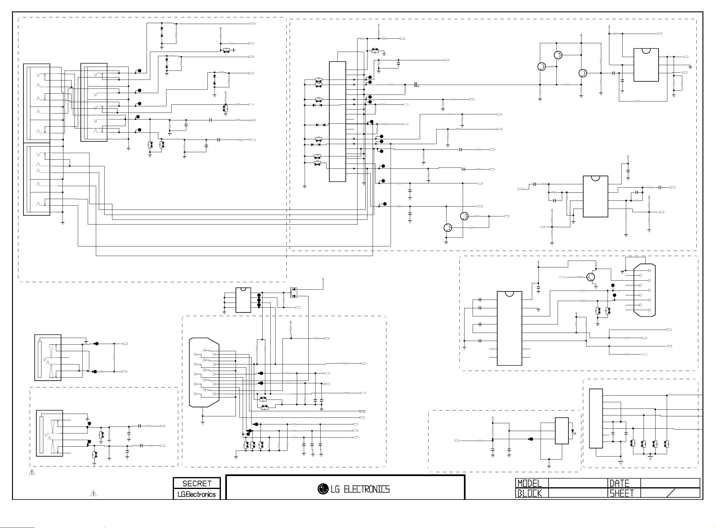
COMPONENT1
Copyright © 2012 LG Electronics Inc. All rights reserved.
Only for training and service purposes
LGE Internal Use Only
NO_EU
PPJ239-01
JK503
6H
[RD1]E-LUG
5H
[RD1]O-SPRING_2
4H
[RD1]CONTACT_2
5G
[WH1]O-SPRING
4F
[RD1]CONTACT_1
5F
[RD1]O-SPRING_1
7F
[RD1]E-LUG-S
5E
[BL1]O-SPRING
7E
[BL1]E-LUG-S
4D
[GN1]CONTACT
5D
[GN1]O-SPRING
6D
[GN1]E-LUG
6N
[RD2]E-LUG
5N
[RD2]O-SPRING_2
4N
[RD2]CONTACT
5M
[WH2]O-SPRING
5L
[RD2]O-SPRING_1
7L
[RD2]E-LUG-S
5K
[BL2]O-SPRING
7K
[BL2]E-LUG-S
4J
[GN2]CONTACT
5J
[GN2]O-SPRING
6J
[GN2]E-LUG
COMPONENT2
WIRED IR
JK502
PEJ027-04
PC AUDIO
PEJ027-04
US
JK500
3
E_SPRING
T_TERMINAL1
6A
B_TERMINAL1
7A
R_SPRING
4
T_SPRING
5
B_TERMINAL2
7B
T_TERMINAL2
6B
3
6A
7A
4
5
7B
6B
E_SPRING
T_TERMINAL1
B_TERMINAL1
R_SPRING
T_SPRING
B_TERMINAL2
T_TERMINAL2
5.6V
D535
PPJ234-02
5.6V
OPT
JK501
D536
OPT
EU
6A
5A
4A
7B
5B
7C
5C
4C
5D
4E
5E
6E
R594
US
22
[GN]E-LUG
[GN]O-SPRING
[GN]CONTACT
[BL]E-LUG-S
[BL]O-SPRING
[RD]E-LUG-S
[RD]O-SPRING_1
[RD]CONTACT_1
[WH]O-SPRING
[RD]CONTACT_2
[RD]O-SPRING_2
[RD]E-LUG
COMP2_LIN
COMP2_RIN
COMP2_DET
NO_US
Near to P901
0
R58 5
C501
R501
1000pF
470K
50V
C500
R502
1000pF
470K
50V
COMP2_Pr
COMP2_Y
COMP2_Pb
IR
IR_TX
D508
5.48VTO5.76V
D500
5.48VTO5.76V
D507
5.6V
C539
10uF
R503
16V
30K
C540
10uF
16V
5.48VTO5.76V
5.48VTO5.76V
D509
5.6V
R504
30K
D510
D501
R516
470K
R507
0
R520
0
PC_R_IN
PC_L_IN
R513
1%
75
1%
R521
470K
R517
75
C503
1000pF
50V
RGB PC
JK507
SPG09-DB-010
6
1
7
2
8
3
9
4
10
5
16
GND
+3.3V_MULTI
D512
5.48VTO5.76V
D502
5.48VTO5.76V
C537
10uF
16V
C510
1000pF
50V
11
12
13
14
15
SHILED
R524
10K
D514
R523
0
1%
+3.3V_MULTI
R525
10K
D513
5.6V
C538
10uF
16V
RED_GND
GND_2
RED
GREEN_GND
DDC_DATA
GREEN
BLUE_GND
H_SYNC
BLUE
NC
V_SYNC
GND_1
SYNC_GND
DDC_CLOCK
DDC_GND
R526
1K
5.6V
R527
75
R528
1K
R518 30K
R52230K
R1EX24002ASAS0A
A0
A1
A2
VSS
GND
B
IC501
AZ4580MTR-E1
1
EU
2
3
4
US
R571
47K
US
C
Q504
MMBT3904(NXP)
E
R564
R565
D528
5.6V
R568
10K
JK506
XRJV-01V-0-D12-080
1
2
3
4
5
6
7
8
9
9
P_+5V
R572
18K
EU
R573
10K
EU
1
2
3
4
5
6
7
8
R590
EU
10K
IC502
NLASB3157DFT2G
SELECT
6
EU
VCC
5
A
4
EU
C534
C536
10uF
16V
0.1uF
EU
16V
R5860
OPT
P_+17V
EU
C529
0.1uF
50V
VCC
8
OUT2
7
IN2-
6
IN2+
5
D529
5.6V
OPT
OPT
R579 0
R576
C543
0.1uF
16V
OPT
D530
5.5V
R578
10K
EU
0
C535
0.1uF
16V
EU
P_+17V
33pF
C533
33K
R575
R582
EU
OPT
R584
OPT
10
9
8
7
6
SPG09-DB-009
JK508
D531
D532
5.5V
5.5V
2.2K
R570
EU
100K
100K
1
2
3
5
4
3
2
1
MICOM_RX
MICOM_TX
DTV_ATV_SELECT
B1
GND
B0
25V
1uF
C547
EU
SC_ROUT
D533
5.5V
R595
75
EU
DTV/MNT_ROUT
RS232_RXD
RS232_TXD
SC_CVBS_OUT
1%
1%
R596
75
EU
ATV_OUT
NO_EU
R583
0
+3.3V_MULTI
R533
10K
D523
5.6V
1%
R532
0
R529
1%
75
R530751%
R536
R531
EU
R534
0
P_+5V
R535
SC/COMP2_DET
R559
220
EU
R577
10K
EU
R567
470
EU
C
Q505
E
MMBT3904(NXP)
EU
R566
180
EU
OUT1
IN1-
IN1+
VEE
E
B
P_+17V
R560
R561
R558
330
100K
100K
Q503
C
MMBT3906(NXP)
EU
EU
EU
R574
33K
C532
33pF
EU
B
R544
75
EU
R546
75
MMBT3904(NXP)
Q500
EU
1%
1%
R545
51K
EU
1%
SC_CVBS_IN
R549
33
EU
R553
10K
EU
R550
0
C541
10uF
16V
Q501
EU
C542
10uF
16V
MMBT3904(NXP)
SC_FB
SC_ID
1%
SC_B/COMP2_Y/AV2_CVBS
SC/COMP2/AV2_L_IN
SC/COMP2/AV2_R_IN
DTV/MNT_LOUT
DTV/MNT_LOUT
DTV/MNT_ROUT
SC_MUTE
510
R554
EU
R555
510
EU
R547
30K
R548
30K
C514
27pF
50V
EU
C517
R539
75
EU
EU
R537
1K
EU
R538
1K
470K
EU
100uF
16V
EU
SC_R/COMP2_Pr
SC_G/COMP2_Pb
R542
470K
R543
470K
EU
C515
6800pF
50V
EU
C516
6800pF
50V
MMBT3904(NXP)
Q502
EU
EU
SC_LOUT
C
E
R557
100
EU
1/4W
C544
1uF
25V
+3.3V_ST
EU
R569
2.2K
OPT
OPT
1K
75
1%
COMP1_Y/AV1_CVBS
COMP1_DET
COMP1_Pb
COMP1_Pr
COMP1_AV1_DET
COMP1/AV1_L_IN
COMP1/AV1_R_IN
SCART
OPT
D516 5.5V
OPT
D517 5.5V
OPT
D518 5.6V
NO_EU
D511
5.48VTO5.76V
NO_EU
D526
5.48VTO5.76V
OPT
D521 5.6V
NO_EU
D503
5.48VTO5.76V
D527 5.6V
D534 5.6V
NO_EU
D519
5.48VTO5.76V
NO_EU
D520
5.48VTO5.76V
NO_EU
D522
5.48VTO5.76V
PSC008-02
SHIELD
23
EU
JK504
22
21
20
19
18
17
16
15
14
13
12
11
10
9
8
7
6
5
4
3
2
1
AV_DET
COM_GND
SYNC_IN
SYNC_OUT
SYNC_GND2
SYNC_GND1
RGB_IO
R_OUT
RGB_GND
R_GND
D2B_OUT
G_OUT
D2B_IN
G_GND
ID
B_OUT
AUDIO_L_IN
B_GND
AUDIO_GND
AUDIO_L_OUT
AUDIO_R_IN
AUDIO_R_OUT
RS232
US
+3.3V_ST
Fiber Optic
4
SHIELD
47K
B
R563
100
100
R562
10K
+5V_ST
IC503
VCC
1
8
OPT
WP
2
7
SCL
3
6
SDA
4
5
R581
4.7K
R580
4.7K
5.6V
D524
5.6V
D525
D506
5.5V
R500
1%
75
1%
D504
5.5V
D505
5.5V
C
R599
BAT54C
10K
D515
OPT
+3.3V_MULTI
R509
10K
R514
0
R515
0
OPT
R508
R505
75
75
1%
R510
R511
R512
R551
10
10
10
A1
A2
EDID_WP
0
OPT
GND
R552
C5230.1uF
C524
0.1uF
C5250.1uF
R519
1K
DSUB_DET
R597
22
DSUB_HSYNC
DSUB_VSYNC
R598
22
C506
C502
10pF
10pF
0
50V
C504
10pF
50V
GND
C508
10pF
50V
GND
C509
10pF
50V
50V
DSUB_R
DSUB_G
DSUB_B
RGB_DDC_SDA
RGB_DDC_SCL
ROM_DW_DA
ROM_DW_CK
SPDIF OUT
SPDIF_OUT
R506
33
C5260.1uF
R556
2.7K
C1+
V+
C1-
C2+
C2-
V-
DOUT2
RIN2
+3.3V_MULTI
C530
10pF
1
2
3
4
5
6
7
8
EAN41348201
OPT
IC500
MAX3232CDR
C527
47pF
50V
VCC
16
GND
15
DOUT1
14
RIN1
13
ROUT1
12
DIN1
11
DIN2
10
ROUT2
9
IR_TX
C528
0.1uF
2F01TC1-CLM97-4F
GND
VCC
VIN
JK505
1
2
3
THE SYMBOL MARK OF THIS SCHEMETIC DIAGRAM INCORPORATES
SPECIAL FEATURES IMPORTANT FOR PROTECTION FROM X-RADIATION.
FILRE AND ELECTRICAL SHOCK HAZARDS, WHEN SERVICING IF IS
ESSENTIAL THAT ONLY MANUFATURES SPECFIED PARTS BE USED FOR
THE CRITICAL COMPONENTS IN THE SYMBOL MARK OF THE SCHEMETIC.
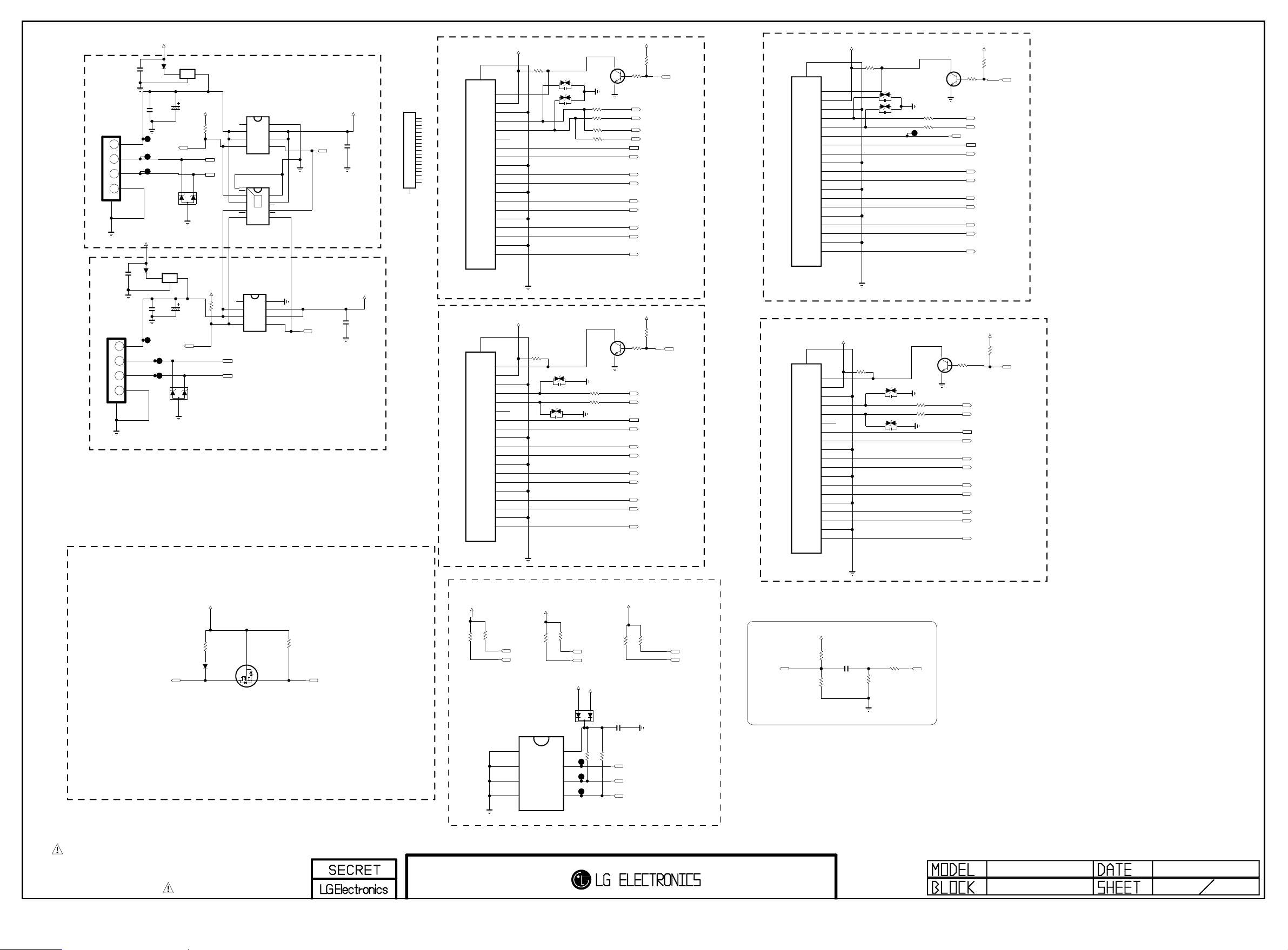
USB1
Copyright © 2012 LG Electronics Inc. All rights reserved.
Only for training and service purposes
LGE Internal Use Only
USB2
10V
10uF
C609
3AU04S-305-ZC-(LG)
JK604
1234
USB DOWN STR EAM
5
+5V_ST
10V
OPT
10uF
B140A
D603
C608
3AU04S-305-ZC-(LG)
JK605
1234
USB DOWN STR EAM
5
+5V_ST
B140A
C600
10uF
10V
D605
IC605
PEN
AP2337SA-7
VIN
3
PEN
1
GND
C605
100uF
16V
OPT
OPT
USB_OCD1
D600
RCLAMP0502BA
IC604
PEN
AP2337SA-7
VOUT
VIN
2
3
PEN
1
GND
OPT
C601
C607
10uF
100uF
10V
16V
USB_OCD2
D601
RCLAMP0502BA
* HDMI CEC
VOUT
2
+3.3V_MULTI
R602
2.7K
USB_DM1
USB_DP1
+3.3V_MULTI
R601
2.7K
NC
OUT_2
OUT_1
FLG
[EP]GND
FLT1
OUT1
OUT2
FLT2
NC
OUT_2
OUT_1
FLG
USB_DM2
USB_DP2
IC600
AP2191DSG
8
7
6
5
EAN61849601
IC603
TPS2062C
8
THERMAL
9
7
6
5
OPT
T-TPS2062C
IC601
AP2191DSG
8
7
6
5
EAN61849601
Q601
Q602
5V_HDMI_1
10K
R624
C
R622
10K
B
HPD1
E
DDC_SDA_1
DDC_SCL_1
OPT
DDC_SDA_4
OPT
DDC_SCL_4
CEC_REMOTE
CK-_HDMI1
CK+_HDMI1
D0-_HDMI1
D0+_HDMI1
D1-_HDMI1
D1+_HDMI1
D2-_HDMI1
D2+_HDMI1
5V_HDMI_2
10K
HDMI4
R625
C
R623
10K
B
HDMI4
E
HDMI4
HPD2
DDC_SDA_2
DDC_SCL_2
CEC_REMOTE
CK-_HDMI2
CK+_HDMI2
D0-_HDMI2
D0+_HDMI2
D1-_HDMI2
D1+_HDMI2
D2-_HDMI2
D2+_HDMI2
HDMI_3
SHIELD
20
19
18
17
16
15
14
13
12
11
10
JK600
HDMI_Screw
EAG59023301
HDMI_4
SHIELD
20
HDMI4
19
18
17
16
15
14
CK+
D0-
9
D0_GND
8
D0+
7
D1-
6
D1_GND
5
D1+
4
D2-
3
D2_GND
2
D2+
1
SHIELD
HDMI_Nomal
JK600-*1
YKF45-7058V
DATA2+
1
DATA2_SHIELD
2
DATA2-
3
DATA1+
4
DATA1_SHIELD
5
DATA1-
6
DATA0+
7
DATA0_SHIELD
8
DATA0-
9
CLK+
10
CLK_SHIELD
11
CLK-
12
CEC
13
NC
14
SCL
15
SDA
16
DDC/CEC_GND
17
+5V_POWER
18
HPD
19
20
P_+5V
GND
1
IN_1
2
IN_2
3
EN
4
GND
1
IN
2
EN1
3
EN2
4
GND
1
IN_1
2
IN_2
3
EN
4
USB_CTL1
C603
0.1uF
P_+5V
C602
0.1uF
USB_CTL2
5V_HDMI_2
R608 1K
HDMI4
R610
MMBT3904(NXP)
5.6V
D608
5.6V
D609
R614 22
R615 22
R627 22
R629 22
MMBT3904(NXP)
1K
5.6V
HDMI4
D602
D607
5.6V
HDMI4
HDMI4
HDMI4
R616 22
R617 22
13
12
11
CK+
10
D0-
9
D0_GND
8
D0+
7
D1-
6
D1_GND
5
D1+
4
D2-
3
D2_GND
2
D2+
1
5V_HDMI_1
JK601
EAG59023302
SIDE_HDMI1(ARC)
5V_HDMI_3
BODY_SHIELD
20
19
18
17
16
15
14
13
12
11
CK+
10
D0-
9
D0_GND
8
D0+
7
D1-
6
D1_GND
5
D1+
4
D2-
3
D2_GND
2
D2+
1
JK602
EAG62611201
SIDE_HDMI2(PC)
5V_HDMI_4
BODY_SHIELD
20
19
18
17
16
15
14
13
12
11
CK+
10
D0-
9
D0_GND
8
D0+
7
D1-
6
D1_GND
5
D1+
4
D2-
3
D2_GND
2
D2+
1
JK603
R628
R626 1K
5V_HDMI_3
1K
MMBT3904(NXP)
5.6V
D610
5.6V
D611
R634 22
Q604
C
E
R635 22
R637
10K
B
HDMI_ARC
10K
R638
DDC_SDA_3
DDC_SCL_3
CEC_REMOTE
HPD3
CK-_HDMI3
CK+_HDMI3
D0-_HDMI3
D0+_HDMI3
D1-_HDMI3
D1+_HDMI3
D2-_HDMI3
D2+_HDMI3
5V_HDMI_4
10K
R639
R636
10K
B
HPD4
DDC_SDA_4
DDC_SCL_4
CEC_REMOTE
MMBT3904(NXP)
5.6V
D612
5.6V
D613
R632 22
R633 22
Q603
C
E
CK-_HDMI4
CK+_HDMI4
D0-_HDMI4
D0+_HDMI4
D1-_HDMI4
D1+_HDMI4
D2-_HDMI4
D2+_HDMI4
EAG62611201
+3.3V_ST
Q600
S
R603
120K
R600
27K
D604
CEC_REMOTE HDMI_CEC
30V
BAT54_SUZHO
G
D
SI1012CR-T1-GE3
THE SYMBOL MARK OF THIS SCHEMETIC DIAGRAM INCORPORATES
SPECIAL FEATURES IMPORTANT FOR PROTECTION FROM X-RADIATION.
FILRE AND ELECTRICAL SHOCK HAZARDS, WHEN SERVICING IF IS
ESSENTIAL THAT ONLY MANUFATURES SPECFIED PARTS BE USED FOR
THE CRITICAL COMPONENTS IN THE SYMBOL MARK OF THE SCHEMETIC.
EDID Pull-up
P_+5V
R604
R606
47K
47K
DDC_SDA_1
DDC_SCL_1
R1EX24002ASAS0A
A0
1
A1
2
A2
3
VSS
4
R618
47K
HDMI4
IC602
P_+5V
OPT
P_+5V
R620
47K
HDMI4
P_+5V
DDC_SDA_2
DDC_SCL_2
5V_HDMI_4
R619
R621
47K
47K
DDC_SDA_3
DDC_SCL_3
HDMI_ARC
P_+5V
R609
1.2K
OPT
R611
100K
10V
C6061uF
R612
82
R613
180
ARC
A2CA1
D606
BAT54C
C604
0.1uF
16V
VCC
8
7
6
5
R605
R607
47K
WP
SCL
SDA
47K
EDID_WP
DDC_SCL_4
DDC_SDA_4
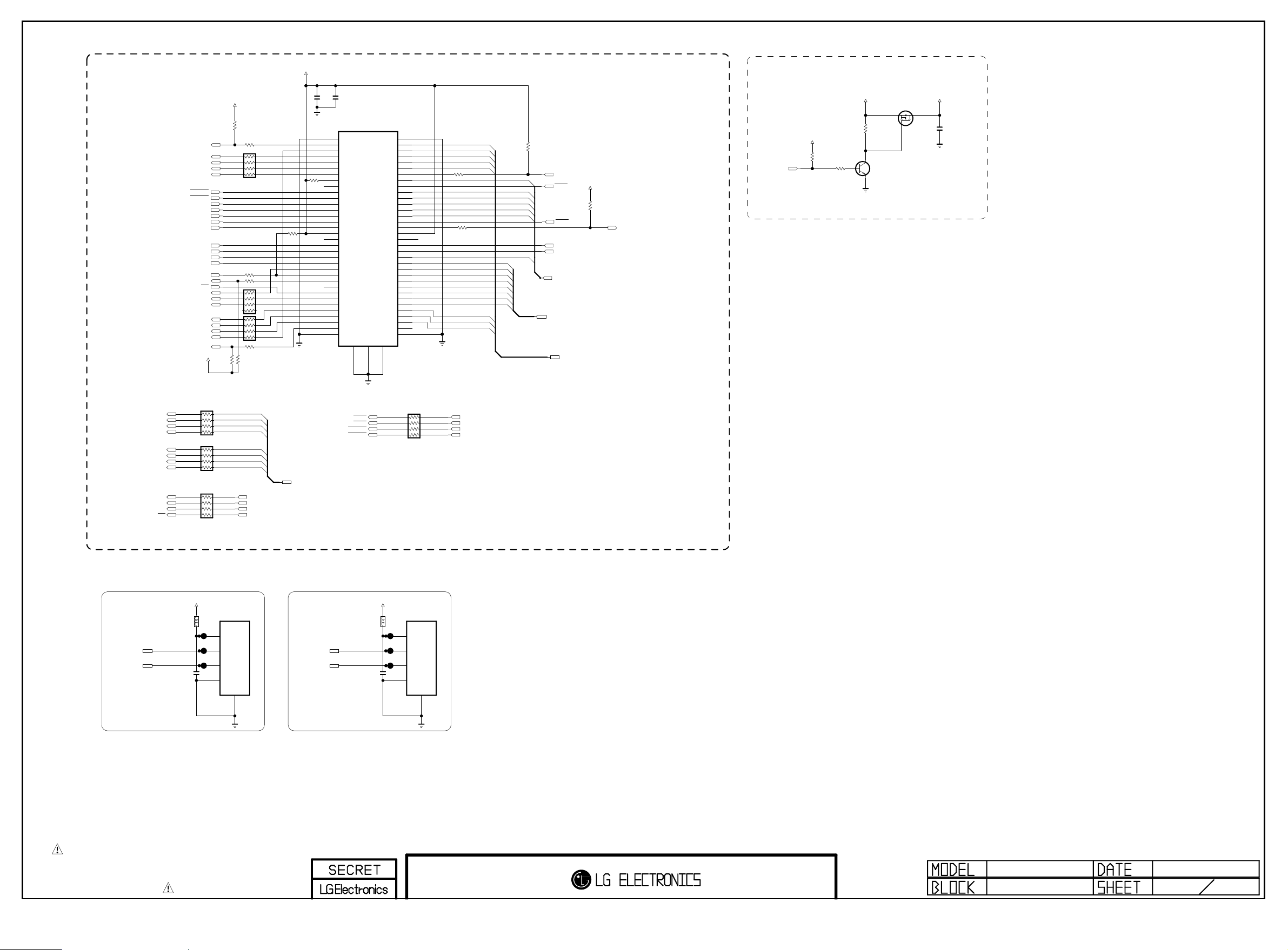
DVB-CI SLOT
Copyright © 2012 LG Electronics Inc. All rights reserved.
Only for training and service purposes
LGE Internal Use Only
/CI_CD1
CI_TS_D[4]
CI_TS_D[5]
CI_TS_D[6]
CI_TS_D[7]
CI_IORD
CI_IOWR
CI_MDI_SYNC
CI_MDI[0]
CI_MDI[1]
CI_MDI[2]
CI_MDI[3]
CI_MDI[4]
CI_MDI[5]
CI_MDI[6]
CI_MDI[7]
PCM_RST
/PCM_WAIT
CI_TS_CLK
CI_TS_VAL
CI_TS_SYNC
CI_TS_D[0]
CI_TS_D[1]
CI_TS_D[2]
CI_TS_D[3]
/CI_CD2
REG
P_+5V
P_+5V
R703
10K
R708 100
AR700
R706
R707
AR701
AR702 33
R710
R704
10K
R702
10K
+5V_CI_ON
CI POWER ENABLE CONTROL
C701
C700
0.1uF
10uF
16V
10V
JK701
EAG41860101
10067972-050LF
35
36
R713
10K
37
38
39
40
41
42
43
44
45
46
47
48
49
50
51
52
53
54
55
56
57
58
59
65
66
67
68
2
33
10K
R711
33
33
33
100
3
4
5
6
7
8
9
10
11
12
13
14
15
16
17
18
19
20
21
22
23
24
25
2660
2761
2862
2963
3064
31
32
33
34
1
G1G2
69
R721 33
R722
PCM_D[3]
PCM_D[4]
PCM_D[5]
PCM_D[6]
PCM_D[7]
100
PCM_A[7]
PCM_A[6]
PCM_A[5]
PCM_A[4]
PCM_A[3]
PCM_A[2]
PCM_A[1]
PCM_A[0]
PCM_D[0]
PCM_D[1]
PCM_D[2]
PCM_A[10]
PCM_A[11]
PCM_A[9]
PCM_A[8]
PCM_A[13]
PCM_A[14]
PCM_A[12]
PCM_D[0-7]
R723
10K
PCM_A[0-7]
PCM_D[0-7]
/PCM_CE
CI_OE
CI_WE
CI_MDI_VAL
CI_MDI_CLK
PCM_A[8-14]
P_+5V
R724
10K
PCM_5V_CTL
/PCM_IRQA
+3.3V_MULTI
R700
4.7K
R701
10K
B
P_+5V
C
E
R705
22K
AO3407A
Q700
MMBT3904(NXP)
Q701
S
+5V_CI_ON
D
C704
G
4.7uF
10V
DVB-CI TS INPUT
CI_MDI[7]
CI_MDI[6]
CI_MDI[5]
CI_MDI[4]
CI_MDI[3]
CI_MDI[2]
CI_MDI[1]
CI_MDI[0]
CI_MDI_CLK
CI_MDI_VAL
CI_MDI_SYNC
REG
WIFI-B/I
WIFI
WIFI_DM3
WIFI_DP3
AR708
47
AR709
47
AR710
47
P_+5V
L700
BLM18PG121SN1D
C702
0.1uF
WIFI
FE_TS_D_OUT[7]
FE_TS_D_OUT[6]
FE_TS_D_OUT[5]
FE_TS_D_OUT[4]
FE_TS_D_OUT[3]
FE_TS_D_OUT[2]
FE_TS_D_OUT[1]
FE_TS_D_OUT[0]
P702
12507WR-04L
1
2
WIFI
3
4
5
FE_TS_CLK_OUT
FE_TS_VAL_OUT
FE_TS_SYNC_OUT
/PCM_REG
FE_TS_D_OUT[0-7]
PEN-B/I
USB_DM4
USB_DP4
CI_OE
CI_WE
CI_IORD
CI_IOWR
P_+5V
L701
PEN
BLM18PG121SN1D
C703
0.1uF
PEN
AR705
33
P703
12507WR-04L
1
2
PEN
3
4
5
/PCM_OE
/PCM_WE
/PCM_IORD
/PCM_IOWR
THE SYMBOL MARK OF THIS SCHEMETIC DIAGRAM INCORPORATES
SPECIAL FEATURES IMPORTANT FOR PROTECTION FROM X-RADIATION.
FILRE AND ELECTRICAL SHOCK HAZARDS, WHEN SERVICING IF IS
ESSENTIAL THAT ONLY MANUFATURES SPECFIED PARTS BE USED FOR
PCMCI Slot/WiFi/PEN
THE CRITICAL COMPONENTS IN THE SYMBOL MARK OF THE SCHEMETIC.
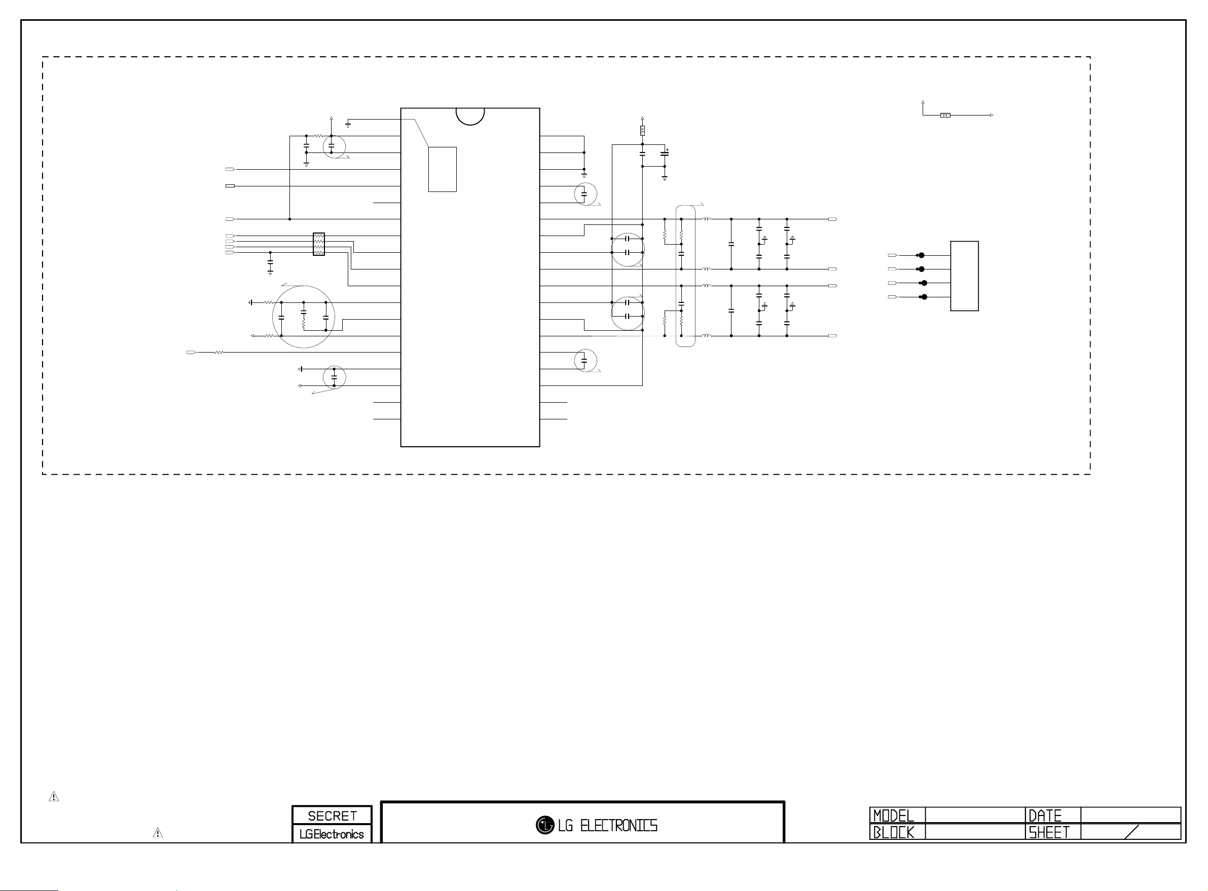
AUDIO AMP [STA368BW]
Copyright © 2012 LG Electronics Inc. All rights reserved.
Only for training and service purposes
LGE Internal Use Only
I2C_SCL1
I2C_SDA1
AMP_RST
AUD_LRCH
AUD_LRCK
AUD_SCK
AUD_MCLK
Close to IC Pin
+3.3V_AMP
R800
AC_DET
1K
OPT
C827
10pF
R801
0
C801
0.1uF
16V
R802
2.2
+3.3V_AMP
Close to IC Pin
IC800
STA368BWG
+3.3V_AMP
R804
10K
C803
0.1uF
16V
AR800 100 R805
C802
4700pF
C804
50V
680pF
50V
R803
2K
[EP]GND
VDD_DIG_2
C805
GND_DIG_2
0.1uF
16V
Close to IC Pin
INT_LINE
RESET
LRCKI
BICKI
GND_PLL
FILTER_PLL
VDD_PLL
PWRDN
GND_DIG_1
C806
0.1uF
VDD_DIG_1
16V
TWARN/OUT4A
EAPD/OUT4B
SCL
SDA
SDI
XTI
36
35
34
33
32
31
30
29
28
27
26
25
24
23
22
21
20
19
THERMAL
37
GND_SUB
1
SA
2
TEST_MODE
3
VSS
4
VCC_REG
5
OUT2B
6
GND2
7
VCC2
8
OUT2A
9
OUT1B
10
VCC1
11
GND1
12
OUT1A
13
GND_REG
14
VDD
15
CONFIG
16
OUT3B/FFX3B
17
OUT3A/FFX3A
18
C807
0.1uF
50V
C808
0.1uF
16V
Close to IC Pin
C809
0.1uF
50V
C810
1uF
25V
C811
0.1uF
50V
C812
1uF
25V
P_+17V
L800
CIS21J121
C813
C814
0.1uF
68uF
50V
35V
R807
39
Close to IC Pin
Close to IC Pin
R808
39
39
C815
330pF
50V
C816
330pF
50V
R806
39
Close to Output PinClose to IC Pin
L801
10.0uH
L802
10.0uH
L803
10.0uH
L804
10.0uH
C817
0.22uF
50V
C818
0.22uF
50V
C819
0.22uF
50V
C820
0.22uF
50V
C821
0.22uF
50V
C822
0.22uF
50V
C823
1000pF
50V
C824
1000pF
50V
C825
1000pF
50V
C826
1000pF
50V
SPK_R-
SPK_R+
SPK_L-
SPK_L+
SPK_R-
SPK_R+
SPK_L-
SPK_L+
+3.3V_MULTI
L805
CIS21J121
JP800
JP801
JP802
JP803
1
2
3
4
WAFER-ANGLE
P800
+3.3V_AMP
THE SYMBOL MARK OF THIS SCHEMETIC DIAGRAM INCORPORATES
SPECIAL FEATURES IMPORTANT FOR PROTECTION FROM X-RADIATION.
FILRE AND ELECTRICAL SHOCK HAZARDS, WHEN SERVICING IF IS
ESSENTIAL THAT ONLY MANUFATURES SPECFIED PARTS BE USED FOR
THE CRITICAL COMPONENTS IN THE SYMBOL MARK OF THE SCHEMETIC.
AMP
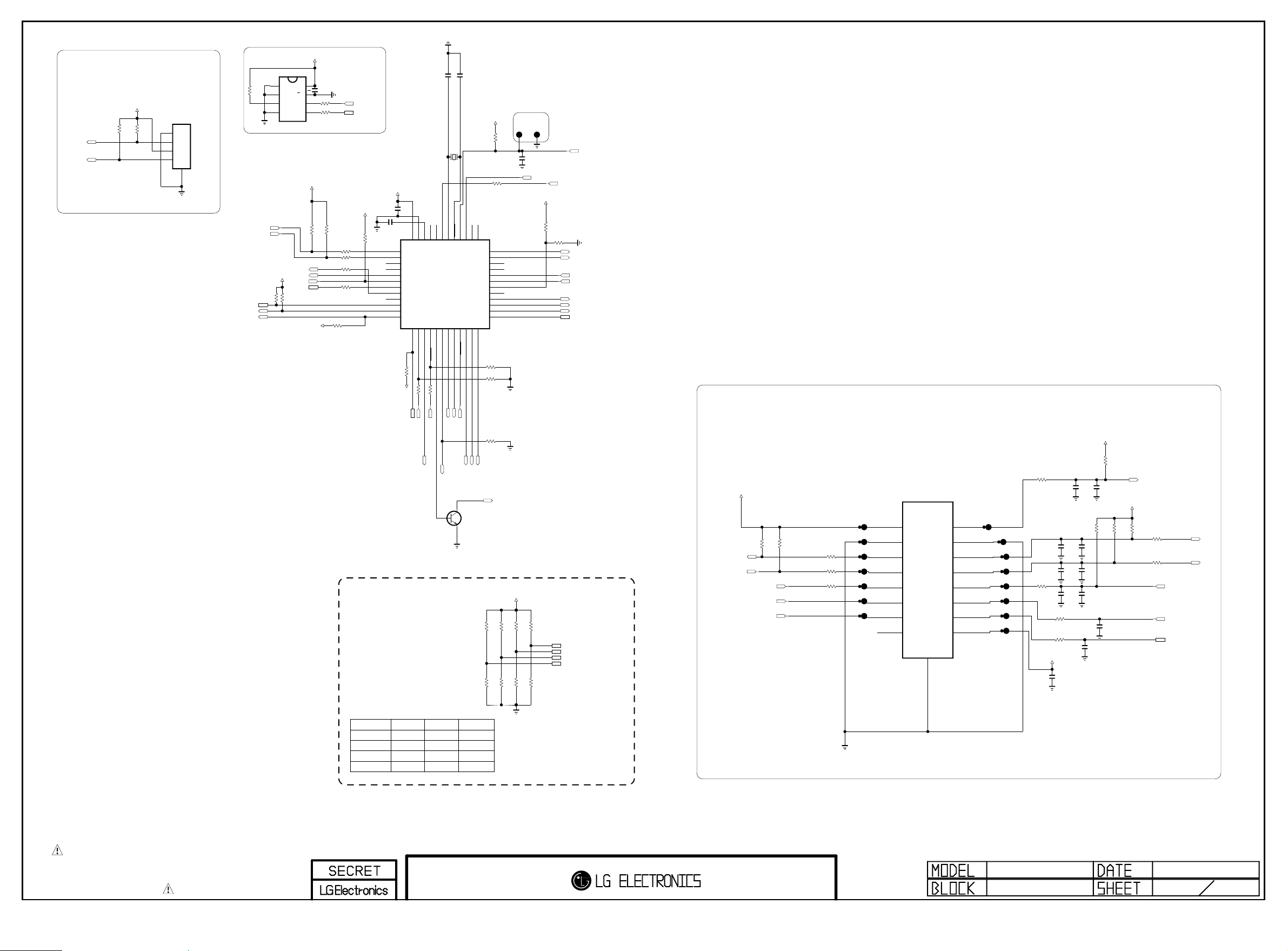
for Debugging
Copyright © 2012 LG Electronics Inc. All rights reserved.
Only for training and service purposes
LGE Internal Use Only
+3.3V_ST
Debug
RESET
R901
DEBUG
10K
DEBUG
R900
DEBUG
1K
PCB TOP
P900
12507WS-04L
1
2
3
4
5
EEPROM_SDA
EEPROM_SCL
SUB_SCL
R903
47K
I2C_SCL3
I2C_SDA3
NC/E0
NC/E1
NC/E2
+3.3V_ST
R912
10K
M24C16-WMN6T
1
2
3
VSS
4
IC900
NC
E1
E2
GND
DISP_EN
LED_R
IR_TX
HDMI_CEC
R913
10K
+3.3V_ST
VCC
8
VCC
WC
7
WC
SCL
6
SCL
SDA
5
SDA
+3.3V_MULTI
R904
10K
OPT
+3.3V_ST
C905
12pF
C900
0.1uF
16V
OPT
R908
22
R909
22
R907
10K
R910 22
R911 22
R949
R916 22
R914
4.7K
EEPROM_SCL
EEPROM_SDA
+3.3V_ST
R917
4.7K
0
+3.3V_ST
C902
1uF
10V
C903
0.1uF
16V
50V
P122/X2/EXCLK
P121/X1
REGC47VSS48VDD
44
45
46
1
2
3
4
IC901
5
6
R5F100GEAFB
7
8
9
10
11
12
13
14
15
16
17
P17/TI02/TO02
P51/INTP2/SO11
R915
4.7K
P16/TI01/TO01/INTP5
P50/INTP1/SI11/SDA11
15K
15K
P15/PCLBUZ1/SCK20/SCL20
R920
R906
+3.3V_ST
AC_DET
SUB_SDA
PSU_ERR_DET
POWER_ON4
X901
32.768KHz
P123/XT1
P137/INTP0
42
43
18
19
P13/TXD2/SO20
P14/RXD2/SI20/SDA20
P12/SO00/TXD0/TOOLTXD
MOD_ON
SOC_RESET
B
MICOM MODEL OPTION
**ALL TOOL : LED_RED
PIN NO.
MODEL1_OPT_0
MODEL1_OPT_2
MODEL1_OPT_3
HIGH
ATSC
8 DVB
11
PZ55
PZ95
30
31
-
C906
12pF
50V
+3.3V_ST
R930
10K
R918
22
P120/ANI19
P41/TI07/TO07
P40/TOOL0
RESET41P124/XT2/EXCLKS
37
38
39
40
20
21
P11/SI00/RXD0/TOOLRXD/SDA00
MICOM_TX
C
E
36
35
34
33
32
31
30
29
28
27
26
25
22
23
24
P146
P147/ANI18
P10/SCK00/SCL00
33K
R928
33K
R929
OPT
R905
100K
MICOM_RX
POWER_ON1
POWER_ON2
POWER_ON3
Q900
MMBT3904(NXP)
OPT
R926 10K
OPT
R927 10K
LOWPIN NAME
PZ75/PZ95MODEL1_OPT_1
PZ55/PZ75
-
P140/PCLBUZ0/INTP6
P00/TI00/TXD1
P01/TO00/RXD1
P130
P20/ANI0/AVREFP
P21/ANI1/AVREFM
P22/ANI2
P23/ANI3
P24/ANI4
P25/ANI5
P26/ANI6
P27/ANI7
EDID_WP
+3.3V_ST
OPT
R931 10K
OPT
R932 10K
PCB TOP
FOR USE MICOM RESET
JP901
JP900
3D_SYNC_RF
R919
10K
OPT
RL_ON
SC_MUTE
KEY2
KEY1
MODEL1_OPT_0
MODEL1_OPT_1
MODEL1_OPT_2
MODEL1_OPT_3
MODEL1_OPT_0
MODEL1_OPT_1
MODEL1_OPT_2
MODEL1_OPT_3
RESET
+3.3V_MULTI
M_REMOTE_RX
M_REMOTE_TX
to Sub Ass’y
R924
2.7K
R925
2.7K
M_REMOTE_RST
M_REMOTE_ISP
3D_SYNC_RF
R935
22
R939
22
R940
22
OPT
JP902
JP903
JP904
JP905
JP906
JP907
JP908
P901
SMAW200-H16S2
1
3
5
7
9
11
13
15
2
4
6
8
10
12
14
16
17
JP909
JP910
JP911
JP912
JP913
JP914
JP915
JP916
R950
22
R953
22
+3.3V_ST
C915
10pF
C916
10pF
C917
10pF
50V
OPT
50V
OPT
50V
R944
R945
C918
10uF
6.3V
+3.3V_ST
R921
4.7K
OPT
+3.3V_ST
R943
10K
IR
R951
22
R952
22
LED_R
SUB_SCL
SUB_SDA
KEY1
KEY2
OPT
C914
C910
10pF
680pF
50V
50V
R947
R946
4.7K
10K
C911
220pF
50V
C912
220pF
50V
C913
10pF
50V
OPT
22
C908
10pF
50V
OPT
22
C909
68pF
50V
C907
0.1uF
16V
Debug
+3.3V_MULTI
R902
10K
10K
OPT
OPT
R936 10K
R933
OPT
OPT
R937 10K
R934 10K
THE SYMBOL MARK OF THIS SCHEMETIC DIAGRAM INCORPORATES
SPECIAL FEATURES IMPORTANT FOR PROTECTION FROM X-RADIATION.
FILRE AND ELECTRICAL SHOCK HAZARDS, WHEN SERVICING IF IS
ESSENTIAL THAT ONLY MANUFATURES SPECFIED PARTS BE USED FOR
THE CRITICAL COMPONENTS IN THE SYMBOL MARK OF THE SCHEMETIC.
MICOM,SUB ASSY
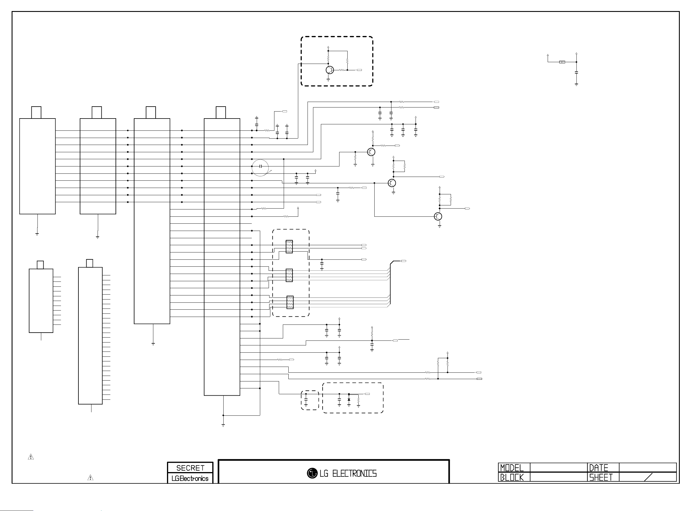
ATSC_CO
Copyright © 2012 LG Electronics Inc. All rights reserved.
Only for training and service purposes
LGE Internal Use Only
12
ATSC_NT
TUNER [DVB-T/C/S2, TDSQ-G001D, H/NIM,F/NIM]
[DVB-T/C, TDSS-G101D, H/NIM]
[DVB-T2/C, TDSN-G301D, F/NIM]
[ATSC-KR/US, TDSS-H101F, H/NIM]
[ATSC-BR, TDSN-B001F, F/NIM]
[ATSC-CO, TDSH-T101F, H/NIM]
TU1003
TDSH-T101F
1
2
3
4
5
6
7
8
9
10
11
SHIELD
TU1001-*1
TDSS-H101F
1
2
3
4
5
6
7
8
9
10
11
12
SHIELD
RF_S/W_CTL
RESET
SCL
SDA
+B1[3.3V]
SIF
+B2[1.8V]
CVBS
IF_AGC
DIF[P]
DIF[N]
NC
RESET
SCL
SDA
+B1[3.3V]
SIF
+B2[1.8V]
CVBS
IF_AGC
DIF[P]
DIF[N]
ATSC_BR
28
DVB_T/C
12
SHIELD
TU1002-*1
TDSN_B001F
RF_S/W_CTL
1
RESET
2
SCL
3
SDA
4
+B1[3.3V]
5
SIF
6
+B2[1.8V]
7
CVBS
8
NC_1
9
NC_2
10
NC_3
11
+B3[3.3V]
12
+B4[1.23V]
13
NC_4
14
GND
15
ERROR
16
SYNC
17
VALID
18
MCLK
19
D0
20
D1
21
D2
22
D3
23
D4
24
D5
25
D6
26
D7
27
SHIELD
TU1001
TDSS-G101D
NC
1
RESET
2
SCL
3
SDA
4
+3.3V
5
SIF
6
+1.8V
7
CVBS
8
IF_AGC
9
DIF[P]
10
DIF[N]
11
DVB_T2
28
SHIELD
TU1002
TDSN-G301D
NC_1
1
RESET
2
SCL
3
SDA
4
+B1[3.3V]
5
SIF
6
+B2[1.8V]
7
CVBS
8
NC_2
9
NC_3
10
NC_4
11
+B3[3.3V]
12
+B4[1.23V]
13
NC_5
14
GND
15
ERROR
16
SYNC
17
VALID
18
MCLK
19
D0
20
D1
21
D2
22
D3
23
D4
24
D5
25
D6
26
D7
27
S
TU1000
TDSQ-G001D
1
2
3
4
5
6
7
8
9
10
11
12
13
14
15
16
17
18
19
20
21
22
23
24
25
26
27
28
29
30
31
32
33
34
35
36
37
38
SHIELD
NC_1
RESET
SCL
SDA
+B1[3.3V]
SIF
+B2[1.8V]
CVBS
T/C_IF_AGC
T/C_DIF[P]
T/C_DIF[N]
NC_2
NC_3
NC_4
GND_1
ERROR
SYNC
VALID
MCLK
D0
D1
D2
D3
D4
D5
D6
D7
GND_2
GND_3
+B3[1.23V]
S2_RESET
+B4[3.3V]
S2_F22_OUTPUT
S2_SCL
S2_SDA
LNB
GND_4
0.1uF
C1021
16V
NO_EU
R1009
1K
BR_CO
C1000
close to TUNER
0.1uF
16V
R1000
0
T2_BR
Close to the tuner
R1002
51
S
Close to Tuner #38 pin
C1019
0.1uF
16V
R1003
0
T2_BR
AR1000
33
1/16W
AR1001
33
1/16W
AR1002
33
1/16W
RF_SW_CTL
C1022
10uF
6.3V
OPT
+1.25V_TU
T2_S_BR
T2_S_BR
T2_S_BR
LNB_TX
CLOSED TO TUNER
MMBT3904(NXP)
+1.8V_TU
C1001
C1003
0.1uF
10uF
16V
6.3V
C1002
1000pF
50V
S
+3.3V_TU_BUF
R1001
10K
C
Q1003
E
DIF_P
DIF_N
OPT
C1017
10pF
50V
+1.25V_TU
C1004
0.1uF
16V
S
C1005
0.1uF
16V
S
Surge protectioin
3.0SMCJ20A(suzhougrande)
R1030
R1008
0
B
C1006
0.047uF
25V
NO_T2_BR
+3.3V_TU
4.7K
C1008
10uF
6.3V
S
C1009
33pF
50V
S
C1007
10uF
6.3V
S
R1007 10K
NO_T2_BR
D1000
S
R1006
4.7K
R1027
2.2K
S
TU_RST
+3.3V_TU_BUF
R1012
470
1/10W
B
IF_AGC
FE_TS_SYNC
FE_TS_VAL
FE_TS_CLK
+3.3V_TU
LNB_OUT
1W
C1011
68pF
50V
R1013
82
E
Q1001
MMBT3906(NXP)
C
FE_TS_D[0]
FE_TS_D[1]
FE_TS_D[2]
FE_TS_D[3]
FE_TS_D[4]
FE_TS_D[5]
FE_TS_D[6]
FE_TS_D[7]
R1011
2.2K
S
0.1uF
16V
C1010
S
C1012
68pF
50V
C1020
0.01uF
50V
+3.3V_TU_BUF
R1014
200
1/10W
E
Q1002
MMBT3906(NXP)
B
C
R1015
22
R1016
22
C1013
0.1uF
16V
TU_SIF
S2_RESET
+3.3V_TU
R1017
200
1/10W
FE_TS_D[0-7]
C1014
10uF
6.3V
+3.3V_TU_BUF
R1004
22 S
R1005
22 S
B
I2C_SCL6
I2C_SDA6
TU_CVBS
R1028
200
EU
1/10W
E
Q1000
MMBT3906(NXP)
EU
C
+3.3V_TU
R1020
R1021
3.3K
3.3K
S
S
R1029
200
EU
1/10W
ATV_OUT
I2C_SCL4
I2C_SDA4
DAC_3V3
L1000
BLM18PG121SN1D
+3.3V_TU_BUF
C1018
0.1uF
16V
THE SYMBOL MARK OF THIS SCHEMETIC DIAGRAM INCORPORATES
SPECIAL FEATURES IMPORTANT FOR PROTECTION FROM X-RADIATION.
FILRE AND ELECTRICAL SHOCK HAZARDS, WHEN SERVICING IF IS
ESSENTIAL THAT ONLY MANUFATURES SPECFIED PARTS BE USED FOR
THE CRITICAL COMPONENTS IN THE SYMBOL MARK OF THE SCHEMETIC.
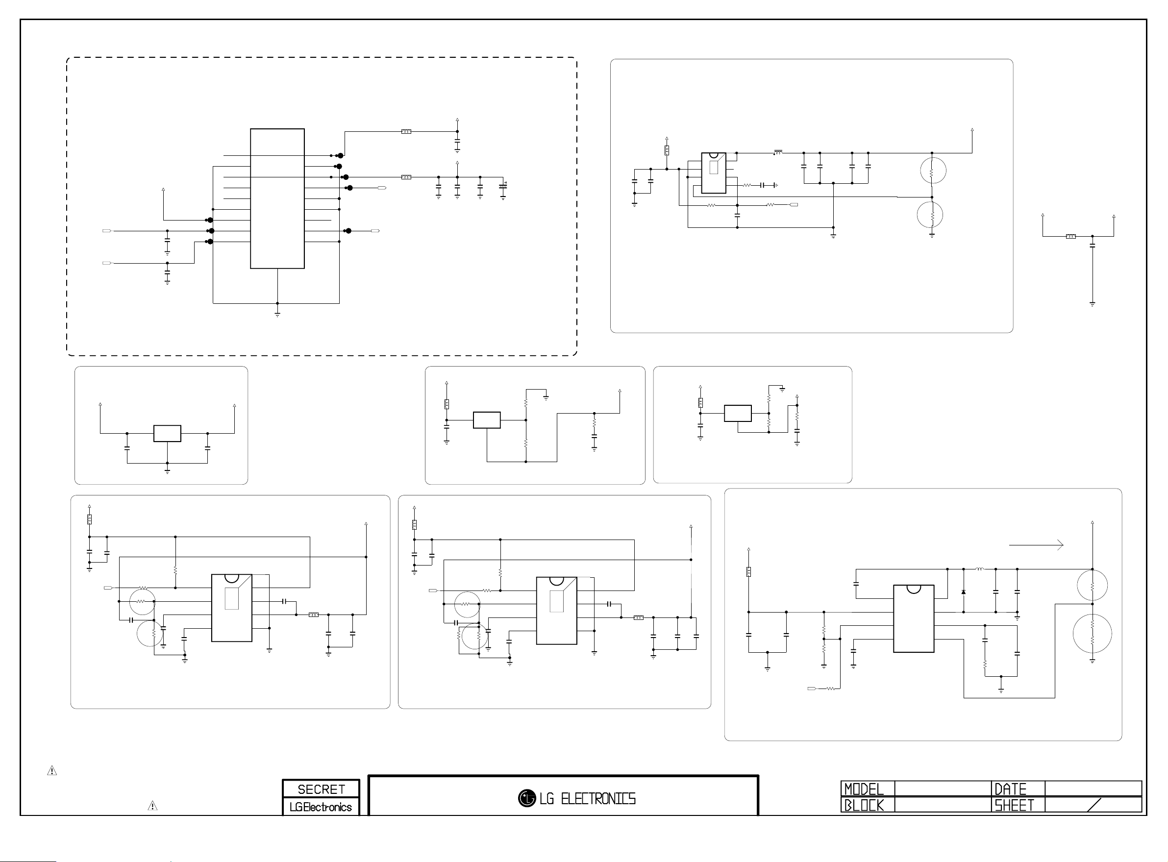
fr. PWR SUPPLY UNIT
Copyright © 2012 LG Electronics Inc. All rights reserved.
Only for training and service purposes
LGE Internal Use Only
+1.2V_CORE_MT5369
+5V_ST
RL_ON
MOD_ON
C1102
0.1uF
16V
C1103
0.1uF
16V
+3.3V_Stand_By
+5V_ST
IC1100
AP2121N-3.3TRE1
VOUT
2
3
1
GND
C1101
0.1uF
16V
VIN
5V_ST
RL_ON
MOD_ON
C1105
1uF
10V
SMAW200-H18S1
17V
GND
5V
NC
NC
GND
+3.3V_ST
1
3
5
7
9
11
13
15
17
P1100
19
2
4
6
8
10
12
14
16
18
17V
GND
5V
PSU_ERR
GND
GND
NC
AC_DET
GND
PSU_ERR_DET
AC_DET
L1100
CIS21J121
L1101
CIS21J121
P_+17V
C1112
0.1uF
50V
P_+5V
C1110
C1113
10uF
0.1uF
10V
16V
+3.3V_MULTI
L1110
T2_S_BR
INPUT ADJ/GND
BLM18PG121SN1D
C1116
10uF
6.3V
T2_S_BR
C1109
C1129
10uF
100uF
10V
16V
+1.25V_TU
T2_S_BR
IC1103
AZ1117BH-ADJTRE1
OUTPUT
240
R1112
T2_S_BR
R1111
1
T2_S_BR
R1113
1
T2_S_BR
C1119
10uF
6.3V
T2_S_BR
*V0=1.25(1+1/240)
1.250000=1.25*(1)
+1.25V_TU
+5V_ST
L1102
CIS21J121
Placed on SMD-TOP
C1108
C1100
10uF
10uF
10V
10V
+1.8V_TU
AOZ1038PI
PGND
1
VIN
2
AGND
3
FB
4
R1120
+3.3V_MULTI
L1109
BLM18PG121SN1D
C1117
10uF
6.3V
L1104
2uH
C1128
10uF
6.3V
C1127
4700pF
50V
R1118
10K
OPT
C1115
16V
0.1uF
POWER_ON1
10K
IC1102
6A
THERMAL
[EP]LX
NC_2
8
NC_1
9
7
EN
6
R1108
3.3K
COMP
5
OPT
Vout=Vref*(1+R1/R2)|Vref=0.8
+1.8V_TU
R1119
1
R2
ADJ/GND
R1
82
1%
R1131
180
5%
R1114
1
C1120
10uF
6.3V
IC1104
AZ1117BH-ADJTRE1
INPUT
3
OUTPUT
*V0=1.25(1+82/180)
=1.8194
2
C1130
10uF
6.3V
C1132
10uF
6.3V
Switching freq: 555K
C1133
10uF
6.3V
R1121
R1122
10K
5.6K
1%
1%
R2
+1.2V_MTK_CORE
R1
+3.3V_MULTI
L1108
BLM18PG121SN1D
C1148
0.1uF
16V
+3.3V_TU
P_+17V
C1151
22uF
6.3V
+3.3V_MULTI
C1152
22uF
6.3V
L1111
BLM18PG121SN1D
C1104
10uF
25V
POWER_ON2
C1106
10uF
25V
IC1101
C1149
3300pF
50V
TPS54327DDAR
EN
VFB
VREG5
SS
1
2
3
4
R1104
R1145
0
R1
1%
R1102
C1107
33K
22pF
50V
R1103
10K
R2
10K
OPT
C1118
1uF
10V
1%
THERMAL
3A
[EP]GND
VIN
8
9
7
6
5
VBST
SW
GND
0.1uF
C1150
16V
L1107
NR5040T2R2N
2.2uH
Vout=0.765*(1+R1/R2)
THE SYMBOL MARK OF THIS SCHEMETIC DIAGRAM INCORPORATES
SPECIAL FEATURES IMPORTANT FOR PROTECTION FROM X-RADIATION.
FILRE AND ELECTRICAL SHOCK HAZARDS, WHEN SERVICING IF IS
ESSENTIAL THAT ONLY MANUFATURES SPECFIED PARTS BE USED FOR
THE CRITICAL COMPONENTS IN THE SYMBOL MARK OF THE SCHEMETIC.
P_+17V
L1112
BLM18PG121SN1D
C1111
10uF
25V
POWER_ON3
+1.5V_DDR
C1141
0.1uF
OPT
50V
-->3.12V
S
S
C1140
0.01uF
50V
17V->12V
IC1106
TPS54231D
BOOT
1
VIN
2
S
EN
3
SS
4
2A
L1106
22.0uH
EAP61606601
S
D1100
40V
SMAB34
PH
8
7
6
5
GND
COMP
VSENSE
S
S
C1144
470pF
50V
S
R1135
51K
*NOTE 13
C1114
10uF
25V
R1117
10K
R1116
0
OPT
1%
R1
R1106
C1121
18K
22pF
50V
C1122
1uF
R1115
10V
51K
R1146
27K
R2
1%
1%
C1123
3300pF
50V
TPS54327DDAR
EN
VFB
VREG5
SS
1
2
3
4
IC1105
3A
9
THERMAL
8
7
6
5
[EP]GND
VIN
VBST
SW
GND
0.1uF
C1124
16V
L1103
NR5040T2R2N
2.2uH
C1125
22uF
6.3V
C1126
22uF
6.3V
C1138
22uF
6.3V
Vout=0.765*(1+R1/R2)
P_+17V
S
L1113
BLM18PG121SN1D
S
C1131
10uF
25V
S
C1135
0.01uF
50V
POWER_ON4
S
R1127
16K
R1128
3.6K
S
R1107
0
S
C1145
10uF
16V
Max 1.3A
S
C1146
10uF
16V
S
C1147
15pF
50V
+12V_LNB
S
R1139
6.8K
1%
R1140
1.6K
1%
R1138
120K
R1
1%
S
R2
S
Vout=0.8*(1+R1/R2)
 Loading...