

Page 1
PLASMA TV
SERVICE MANUAL
CAUTION
BEFORE SERVICING THE CHASSIS,
READ THE SAFETY PRECAUTIONS IN THIS MANUAL.
CHASSIS : PD02A
MODEL : 50PK950/950N/960
50PK950-ZA/50PK950N-ZA
50PK960-ZA
North/Latin America http://aic.lgservice.com
Europe/Africa http://eic.lgservice.com
Asia/Oceania http://biz.lgservice.com
Internal Use Only
Printed in Korea
P/NO : MFL62861603(1003-REV00)
Page 2

- 2 -
LGE Internal Use OnlyCopyright ©2010 LG Electronics Inc. All rights reserved.
Only for training and service purposes
CONTENTS
CONTENTS ............................................................................................................................... 2
SAFETY PRECAUTIONS ...........................................................................................................3
SPECIFICATION.........................................................................................................................4
ADJUSTMENT INSTRUCTION ..................................................................................................6
BLOCK DIAGRAM ...................................................................................................................10
EXPLODED VIEW ................................................................................................................... 11
SVC. SHEET ................................................................................................................................
Page 3
- 3 -
LGE Internal Use OnlyCopyright ©2010 LG Electronics Inc. All rights reserved.
Only for training and service purposes
SAFETY PRECAUTIONS
Many electrical and mechanical parts in this chassis have special safety-related characteristics. These parts are identified by in
the Schematic Diagram and Exploded View.
It is essential that these special safety parts should be replaced with the same components as recommended in this manual to
prevent X-RADIATION, Shock, Fire, or other Hazards.
Do not modify the original design without permission of manufacturer.
General Guidance
An isolation Transformer should always be used during the
servicing of a receiver whose chassis is not isolated from the AC
power line. Use a transformer of adequate power rating as this
protects the technician from accidents resulting in personal injury
from electrical shocks.
It will also protect the receiver and it's components from being
damaged by accidental shorts of the circuitry that may be
inadvertently introduced during the service operation.
If any fuse (or Fusible Resistor) in this monitor is blown, replace it
with the specified.
When replacing a high wattage resistor (Oxide Metal Film
Resistor, over 1W), keep the resistor 10mm away from PCB.
Keep wires away from high voltage or high temperature parts.
Due to high vacuum and large surface area of picture tube,
extreme care should be used in handling the Picture Tube.
Do not lift the Picture tube by it's Neck.
Leakage Current Cold Check(Antenna Cold Check)
With the instrument AC plug removed from AC source, connect
an electrical jumper across the two AC plug prongs. Place the
AC switch in the on position, connect one lead of ohm-meter to
the AC plug prongs tied together and touch other ohm-meter
lead in turn to each exposed metallic parts such as antenna
terminals, phone jacks, etc.
If the exposed metallic part has a return path to the chassis, the
measured resistance should be between 1MΩ and 5.2MΩ.
When the exposed metal has no return path to the chassis the
reading must be infinite.
An other abnormality exists that must be corrected before the
receiver is returned to the customer.
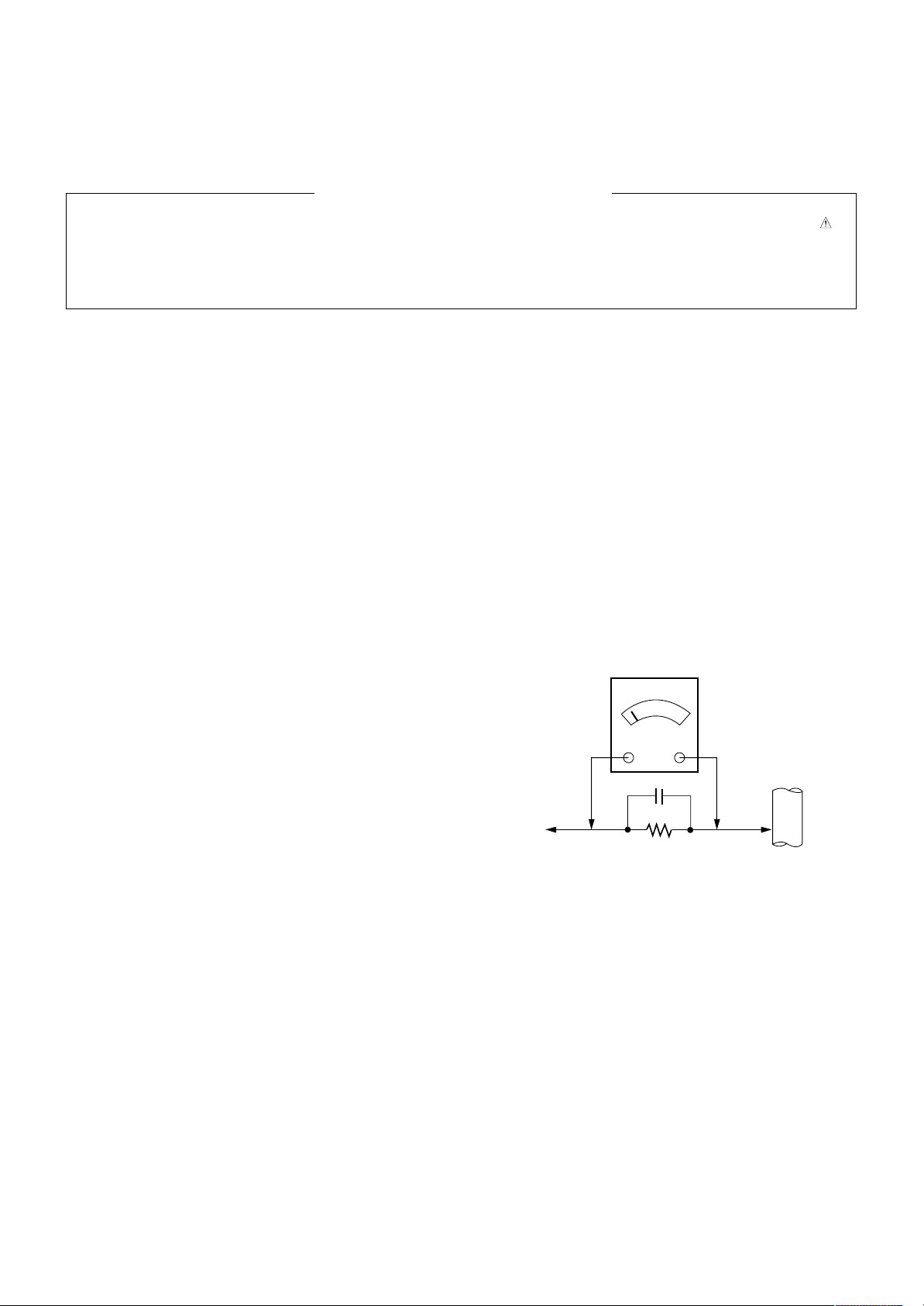
Leakage Current Hot Check (See below Figure)
Plug the AC cord directly into the AC outlet.
Do not use a line Isolation Transformer during this check.
Connect 1.5K/10watt resistor in parallel with a 0.15uF capacitor
between a known good earth ground (Water Pipe, Conduit, etc.)
and the exposed metallic parts.
Measure the AC voltage across the resistor using AC voltmeter
with 1000 ohms/volt or more sensitivity.
Reverse plug the AC cord into the AC outlet and repeat AC
voltage measurements for each exposed metallic part. Any
voltage measured must not exceed 0.75 volt RMS which is
corresponds to 0.5mA.
In case any measurement is out of the limits specified, there is
possibility of shock hazard and the set must be checked and
repaired before it is returned to the customer.
Leakage Current Hot Check circuit
1.5 Kohm/10W
To Instrument's
exposed
METALLIC PARTS
Good Earth Ground
such as WATER PIPE,
CONDUIT etc.
AC Volt-meter
IMPORTANT SAFETY NOTICE
0.15uF
Page 4
- 4 -
LGE Internal Use OnlyCopyright ©2010 LG Electronics Inc. All rights reserved.
Only for training and service purposes
SPECIFICATIONS
NOTE : Specifications and others are subject to change without notice for improvement
.
V Application Range
This spec is applied to PDP TV used PD02A Chassis.
V Specification
Each part is tested as below without special appointment.
(1) Temperature : 25 °C ± 5 °C (77 °F ± 9 °F), CST : 40 ± 5
(2) Relative Humidity: 65 % ± 10 %
(3) Power Voltage: Standard Input voltage (100 V - 240 V ~, 50 / 60 Hz)
* Standard Voltage of each product is marked by models.
(4) Specification and performance of each parts are followed each drawing and specification by part number in accordance with
SBOM.
(5) The receiver must be operated for about 20 minutes prior to the adjustment.
V Test Method
(1) Performance : LGE TV test method followed.
(2) Demanded other specification
Safety : CE, IEC specification
EMC : CE, IEC
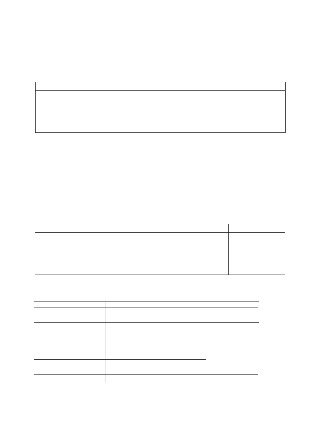
V Module Specification
(1) 50” FHD
No Item Specification Remark
1 Display Screen Device 127 cm (50 inch) wide Color Display Module PDP
2 Aspect Ratio 16:9
3 PDP Module PDP50R1####,
RGB Closed (Well) Type, Glass Filter (38%)
Pixel Format: 1920 horiz. By 1080 ver
4 Operating Environment 1) Temp. : 0 deg ~ 40 deg
2) Humidity : 20 % ~ 80%
5 Storage Environment 3) Temp. : -20 deg ~ 60 deg LGE SPEC
4) Humidity : 10 % ~ 90 %
6 Input Voltage AC 100 V ~ 240 V, 50 / 60 Hz Maker LG
Model Name
50PK950-ZA
50PK950N-ZA
50PK960-ZA
Brand
LG
Market
Albania, Austria, Belgium, Bosnia, Bulgaria, Coratia, Czech, Denmark,
Estonia, Finland, France, Germany, Greece, Hungary, Ireland, Italy,
Kazakhstan, Latvia, Lithuania, Luxembourg, Morocco, Netherlands, Norway,
Poland, Portugal, Romania, Russia, Serbia, Slovakia, Slovenia, Spain,
Sweden, Switzerland, Turkey, Ukraine, UK
Model Name
50PK950-ZA
50PK950N-ZA
50PK960-ZA
Brand
Safety : IEC/EN60065
EMI : EN55013
EMS : EN55020LG
Market
Albania, Austria, Belgium, Bosnia, Bulgaria, Coratia, Czech, Denmark,
Estonia, Finland, France, Germany, Greece, Hungary, Ireland, Italy,
Kazakhstan, Latvia, Lithuania, Luxembourg, Morocco, Netherlands,
Norway, Poland, Portugal, Romania, Russia, Serbia, Slovakia,
Slovenia, Spain, Sweden, Switzerland, Turkey, Ukraine, UK
Page 5
- 5 -
LGE Internal Use OnlyCopyright ©2010 LG Electronics Inc. All rights reserved.
Only for training and service purposes
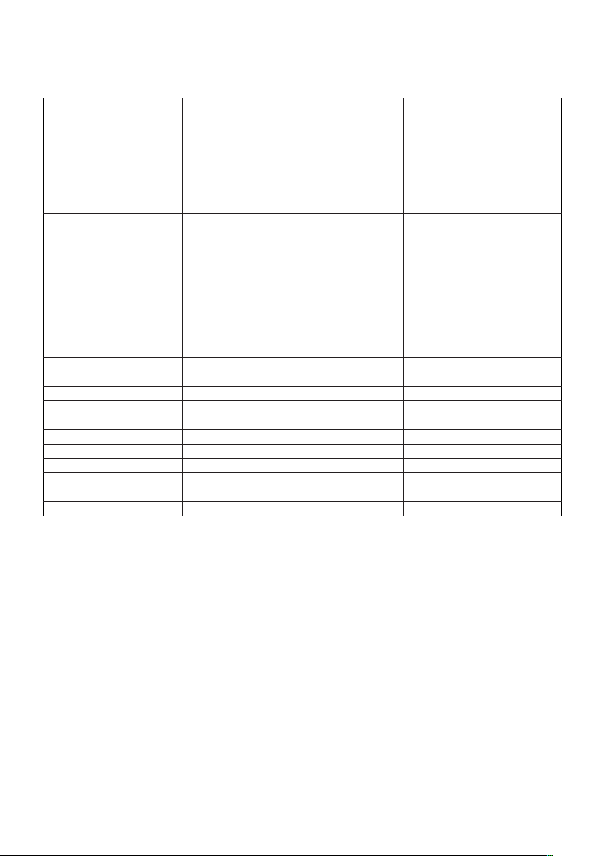
V Model General Specification
No Item Specification Remarks
1 Market Albania, Austria, Belgium, Bosnia, Bulgaria, Coratia, 36 Country
Czech, Denmark, Estonia, Finland, France, Germany,
Greece, Hungary, Ireland, Italy, Kazakhstan, Latvia,
Lithuania, Luxembourg, Morocco, Netherlands, Norway,
Poland, Portugal, Romania, Russia, Serbia, Slovenia,
Spain, Sweden, Slovakia, Switzerland, Turkey, Ukraine,
UK
2 Broadcasting system 1) PAL/SECAM BG EU (PAL Market)
2) PAL/SECAM DK
3) PAL Ⅰ/Ⅱ
4) SECAM L/L’
5) DVB T
6) DVB C DVB C (only Sweden, Finland)
3 Receiving system Analog : Upper Heterodyne
Digital : COFDM
4 Scart Jack (1EA) PAL, SECAM Scart 1 Jack is Full scart and support
RF-OUT(Analog), MNT-OUT
5 Video Input (1EA) PAL, SECAM, NTSC Side AV
6 Component Input (1EA) Y/Cb/Cr, Y/ Pb/Pr
7 RGB Input RGB-PC Analog (D-Sub 15Pin)
8 HDMI Input (4EA) HDMI-PC HDMI/DTV,HDMI2, HDMI3, HDMI4
HDMI-DTV
9 Audio Input (3 EA) RGB/DVI Audio, Component, AV L/R Input
10 SPDIF Out(1 EA) SPDIF Out
11 USB(2EA) For SVC, S/W Download, X-Studio, DivX
12 Bluetooth Bluetooth Phone(JPEG, MP3), Profile : A2DP, BIP, FTP, GAVDP,
Bluetooth Headset(mono, stereo) HSP, OPP
13 Ethernet LAN
Page 6
- 6 -
LGE Internal Use OnlyCopyright ©2010 LG Electronics Inc. All rights reserved.
Only for training and service purposes
ADJUSTMENT INSTRUCTION
1. Application Range
This spec sheet is applied to all of the PD02A chassis.
2. Specification
(1) Because this is not a hot chassis, it is not necessary to use
an isolation transformer. However, the use of isolation
transformer will help protect test instrument.
(2) Adjustment must be done in the correct order.
(3) The adjustment must be performed in the circumstance of
25 °C ± 5 °C of temperature and 65 % ± 10 % of relative
humidity if there is no specific designation.
(4) The input voltage of the receiver must keep 100 V ~ 240
V, 50 / 60 Hz.
(5) The receiver must be operated for about 5 minutes prior to
the adjustment when module is in the circumstance of over
15 °C
- In case of keeping module is in the circumstance of 0 °C,
it should be placed in the circumstance of above 15 °C
for 2 hours
- In case of keeping module is in the circumstance of below
-20 °C, it should be placed in the circumstance of above
15 °C for 3 hours,.
O After RGB Full White in HEAT-RUN Mode, the receiver
must be operated prior to the adjustment.
O Enter into HEAT-RUN MODE
1) Press the POWER ON KEY on R/C for adjustment.
2) OSD display and screen display PATTERN MODE.
- Set is activated HEAT run without signal generator in this
mode.
- Single color pattern ( WHITE ) of HEAT RUN MODE uses
to check panel.
- Caution : If you turn on a still screen more than 20
minutes (Especially digital pattern, cross hatch pattern),
an after image may be occur in the black level part of the
screen.
3.
PCB Assembly Adjustment Method
* Caution: Using ‘power on’ button of the control R/C power on
TV.
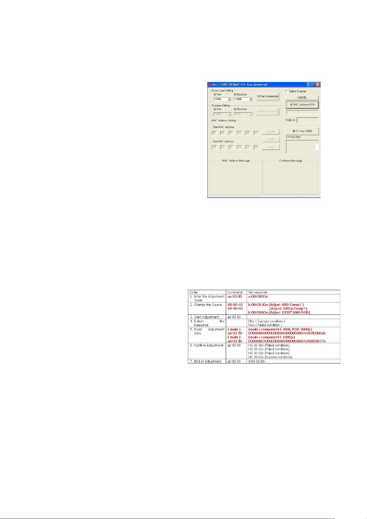
3-1. MAC Address and CI+ Key.
* Connect TV SET and PC which download MAC Address
Writing program by RS232C-Cable
(1) Start “MAC+CIKeyl.exe”Program and Click (3) Button to
connect TV and PC.
(2) Click (4) to download MAC Address.
(3) Click (5) to download CI+ Key.
(4) When download succeed, you can see “OK” on (6)
* Each Chassis has it’ own MAC Address. Please be careful of
download.
3-2. Ping TEST
* This test is to check Network operation.
(1) Press "Power on" button of a service R/C.(Baud rate :
115200 bps)
(2) Connect RS232-C Signal Cable.
(3) Connect LAN cable to MAIN PCB Assembly.
(4) When network operates normally, you can see “OK”.
3-3. ADC Adjustment
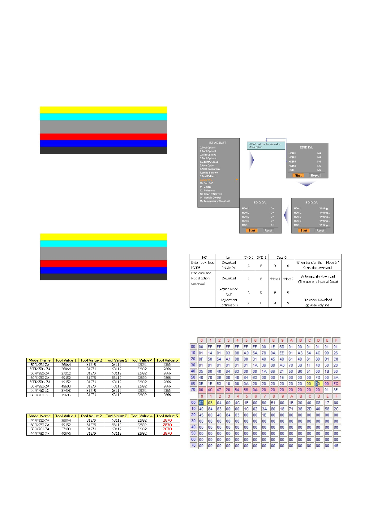
O Auto-control adjustment protocol(RS-232C)
Page 7
- 7 -
LGE Internal Use OnlyCopyright ©2010 LG Electronics Inc. All rights reserved.
Only for training and service purposes
(1) Adjustment of RGB
1) Convert to PC in Input-source.
2) Signal equipment displays
Output Voltage: 700 mVp-p
Impress Resolution FHD (1920 x 1080 @ 60Hz)
Model : 225 in Pattern Generator
Pattern : 65 in Pattern Generator
(MSPG-925 SERISE)
3) Adjust by commanding AUTO_COLOR_ADJUST
(2) COMPONENT input ADC
V Convert to Component in Input-source.
V Signal equipment displays
Impress Resolution 480i
MODEL : 209 in Pattern Generator(480i Mode)
PATTERN : 65 in Pattern Generator
(MSPG-925 SERISE)
Impress Resolution 1080i
MODEL: 225 in Pattern Generator(1080P Mode)
PATTERN: 65 in Pattern Generator
(MSPG-925 SERISE)
3-4. Insert Tool OPTION
(1) Press ADJ key on R/C to insert Tool OPTION
(2) On the “ Tool Option”, Insert Tool Option by a number key
(3) Press the ENTER(
V)
(4) Press ENTER(
V) again.
(5) Select “OK to Download” by using
F/G(VOL +/-) and
press
G(VOL +)
* FOR EU
* FOR France
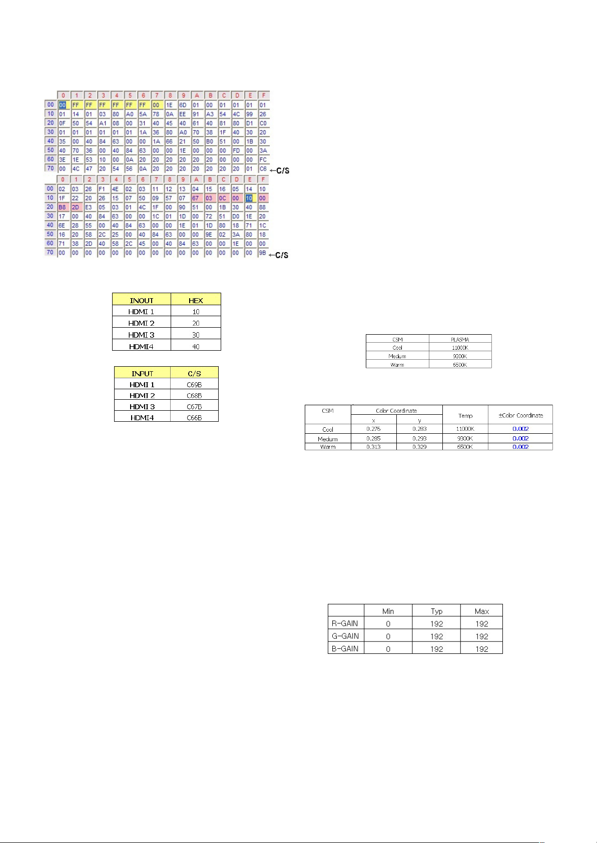
3-5. EDID(The Extended Display
Identification Data) download
(1) Press the ADJ KEY on R/C and enter EZ ADJUST.
(2) Select “5.EDID D/L” by using
D/E(CH +/-) and press
ENTER(
V).
(3) Select “Start” and press navigation key(
G).
(4) EDID download is executed automatically.
(5) Press EXIT key on R/C
* Caution
- Never connect HDMI & D-sub Cable when the user
download EDID .
V Use the proper cables below for EDID Writing.
* Edid data and Model option download(RS232)
* EDID DATA
1) analog RGB
Page 8
- 8 -
LGE Internal Use OnlyCopyright ©2010 LG Electronics Inc. All rights reserved.
Only for training and service purposes
2) HDMI
ⓐ Vender ID
3-6. Confirmation
(1) Press ‘InStart’ Key on Factory SVC Remote Controller.
And MUST check ADC & EDID ADJ status is OK.
4. SET assembly adjustment method
* Caution : Each PCB assembly must be checked by check JIG
set. (Because power PCB Assembly damages to PDP
Module, especially be careful)
4-1. POWER Supply Unit PCB Ass’y
Va/Vs Voltage Adjustment
Test equipment : D.M.M 1EA
Connection Diagram for Measuring : refer to fig.4
Adjustment method
(1) Va adjustment
1) Connect + terminal of D.M.M. to Va pin of P811, connect
-terminal to GND pin of P811.
2) After turning VR502,voltage of D.M.M adjustment as
same as Va voltage which on label of panel right/top
(deviation; ±0.5V)
(2) Vs adjustment
1) Connect + terminal of D.M.M. to Vs pin of P811, connect
-terminal to GND pin of P811.
2) After turning VR901, voltage of D.M.M adjustment as
same as Vs voltage which on label of panel right/top
(deviation ; ±0.5V)
4-2. Download Serial number (RS-232C)
V Press “Power on” key of service R/C.
(Baud rate : 115200 bps)
V Connect RS232 Signal Cable to RS-232 Jack.
V Write Serial number by use RS-232.
V Must check the serial number at the Diagnostics of SET UP
menu.
(Refer to below ‘6.SET INFORMATION’).
4-3. Adjustment of White Balance
Required Equipment
O Remote controller for adjustment
O Color Analyzer ( CS-1000, CA-100,100+,CA-210 or same
produc: CH 10 (PDP)
* Please adjust CA-210, CA-100+ by CS-1000 before
measuring
O Auto W/B adjustment instrument(only for Auto adjustment)
O 9 Pin D-Sub Jack(RS232C) is connected to the AUTO W/B
EQUIPMENT.
Before Adjust of White Balance, Please press POWER ONLY
key
Adjust Process will start by execute RS232C Command.
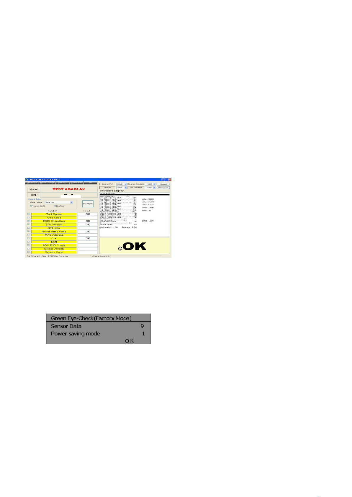
O Color temperature standards according to CSM and Module
O CS-1000/CA-100+/CA-210(CH 10)
White balance adjustment coordinates and color temperature.
* Manual W/B process (using adjusts Remote control)
Please Adjust in AV 1 MODE, Turn off Energy Saving Mode.
(1) Enter ‘PICTURE RESET’ on Picture Mode, then turn off
Fresh Contrast and Fresh colour in Advanced Control
(2) After enter Service Mode by pushing “ADJ” key,
(3) Enter White Pattern off of service mode, and change off ->
on.
(4) Enter “W/B ADJUST” by pushing “
G” key at “3. W/B
ADJUST”.
* Gain Max Value is 192. So, Never make any Gain Value over
192 and please fix one Value on 192, between R, G and B.
Page 9
- 9 -
LGE Internal Use OnlyCopyright ©2010 LG Electronics Inc. All rights reserved.
Only for training and service purposes
* Auto-control interface and directions
(1) Adjust in the place where the influx of light like floodlight
around is blocked. (Illumination is less than 10ux).
(2) Measure and adjust after sticking the Color Analyzer (CA-
100+, CA210 ) to the side of the module.
(3) Aging time
After aging start, keep the Power on (no suspension of
power supply) and heat-run over 5 minutes
4-4. Serial number download & Model
name D/L and Check Tool Option.
(1) Press "Power on" button of a service R/C.(Baud rate :
115200 bps)
(2) Connect RS232-C Signal Cable and start ‘Option Check
Program Ver3.8’
(3) Scan serial Number and press ‘F5’ button.
(4) Check ‘OK’ on program 1) program.
(5) Press ‘In start’ button on SVC R/C, check Serial Number
and Model Name.
4-5. Checking the EYE-Q Operation.
(1) Press the EYE Key on the adjustment remote controller.
(2) Check the Sensor DATA ( It must be under 10) and keep
the data longer than 1.5s
3) Check ‘OK’
(Sensor DATA 0 ~ 4095, Power Saving Mode 0 ~ 12)
* IF you press IN-STAP Button, change Green Eye-check OSD.
4-6. Ping TEST
* This test is to check Network operation.
(1) Connect LAN cable from Computer to TV Set
(2) When network operates normally, you can see “OK” on
Computer
5. Set Information
(Serial No & Model name)
5-1. Check the serial number
& Model Name
(1) Push the menu button and press red button on R/C to
enter ‘Customer Support’menu.
(2) Move to ‘signal test’ menu. And check Serial No & Model
Name
Select the STATION -> Diagnostics -> To set
6. SW Download Guide.
* Before put a *.epk to USB Stick make ‘LG_DTV’ folder in USB.
Then, put *.epk file to ‘LG_DTV’ folder and Turn on TV
(1) Put the USB Stick to the USB socket
(2) Automatically detecting update file in USB Stick
* If your downloaded program version in USB Stick is Low,
it didn’t work.
But your downloaded version is High, USB data is
automatically detecting.
(3) Show the message “Copying files from memory”
(4) Updating is staring.
(5) Updating Completed, The TV will restart automatically.
After turn on TV, Please press ‘IN-STOP’ button on ADJ
Remote-control.
* IF you don’t have ADJ R/C, enter ‘Factory Reset’ in
OPTION MENU.
(6) When TV turns on, check the Updated version on
Diagnostics MENU.
Page 10
- 10 -
LGE Internal Use OnlyCopyright ©2010 LG Electronics Inc. All rights reserved.
Only for training and service purposes
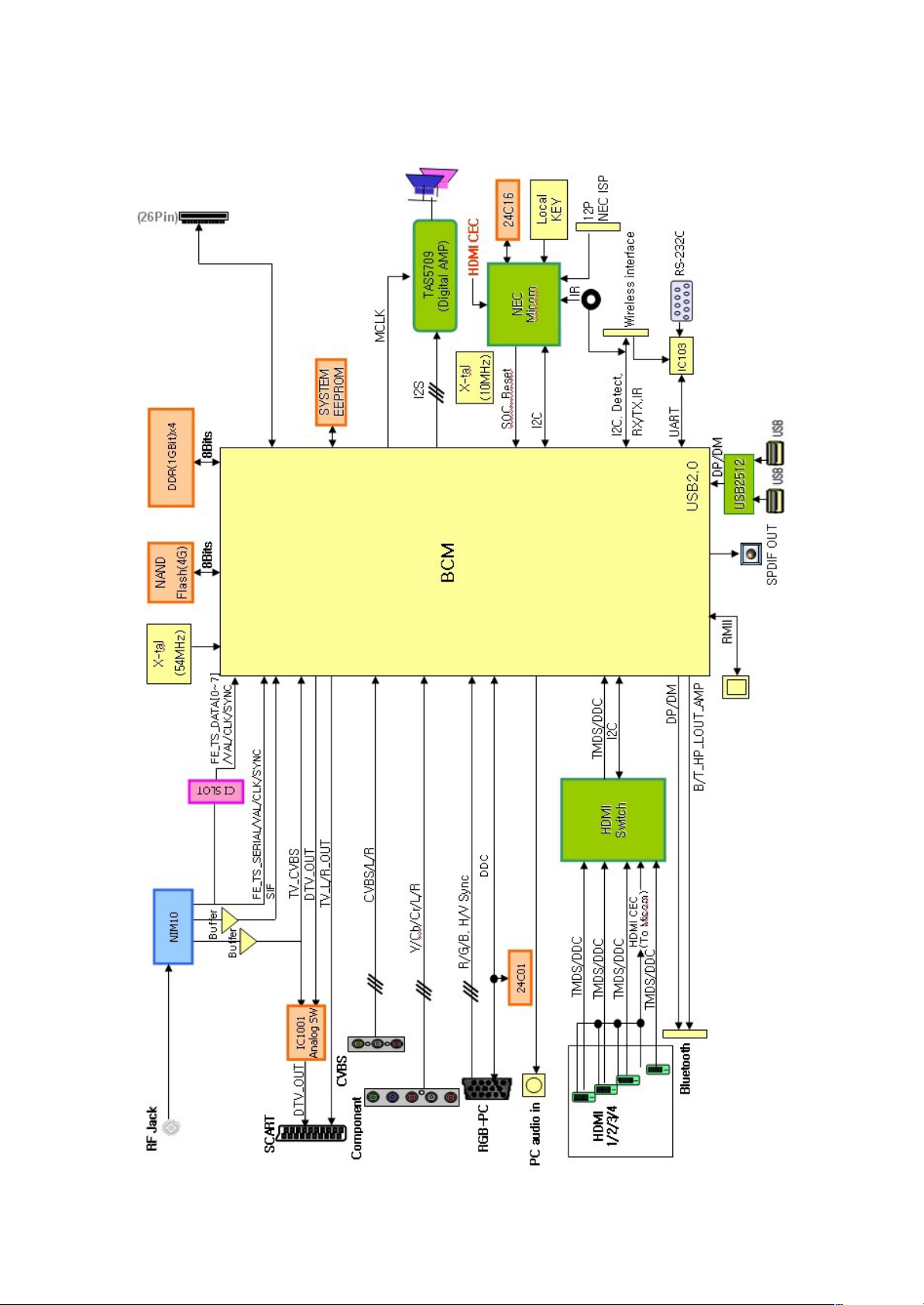
BLOCK DIAGRAM
Page 11
- 11 -
LGE Internal Use Only
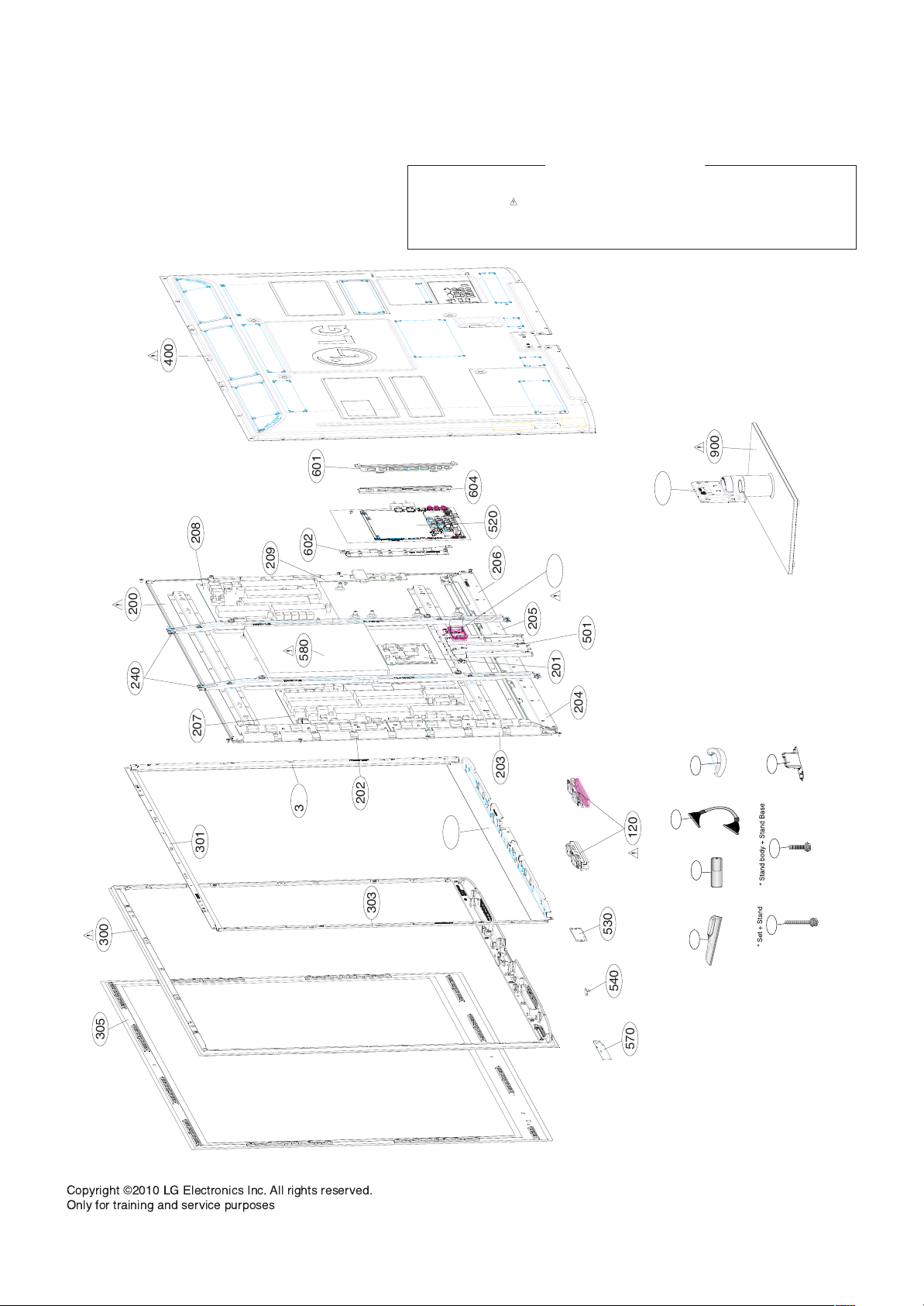
EXPLODED VIEW
Copyright ©2010 LG Electronics Inc. All rights reserved.
Only for training and service purposes
305
570
207
530
203
202
303
602
501
540
900
400
208
580
300
120
200
209
601
520
604
204
201
206
205
240
301
302
304
590
910
Many electrical and mechanical parts in this chassis have special safety-related characteristics. These
parts are identified by in the Schematic Diagram and EXPLODED VIEW.
It is essential that these special safety parts should be replaced with the same components as
recommended in this manual to prevent X-RADIATION, Shock, Fire, or other Hazards.
Do not modify the original design without permission of manufacturer.
IMPORTANT SAFETY NOTICE
A10
A9
LV1
A12
A2
A22
A7
Page 12
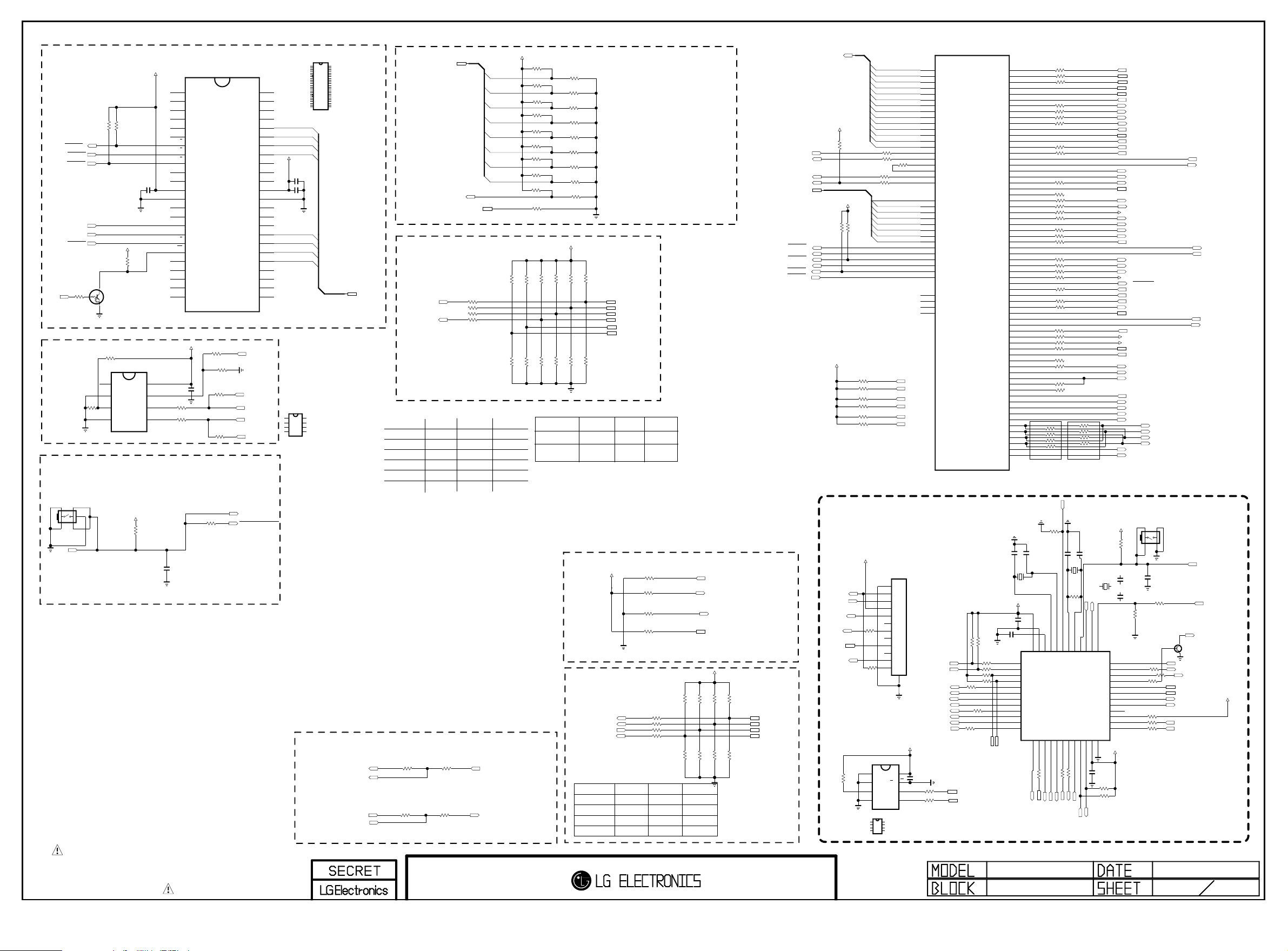
NAND FLASH MEMORY 4G BIT FOR BBTV
Copyright © 2010 LG Electronics Inc. All rights reserved.
Only for training and service purposes
LGE Internal Use Only
BCM REVIEW
R5 2.7K
R4 2.7K
C101
D3.3V
R8
10K
C
Q100
B
KRC103S
E
FLASH_WP
NAND_RB
NAND_RE
NAND_CE
NAND_CLE
NAND_ALE
NAND_WE
R76
0
D3.3V
Open Drain
0.1uF
NC_1
NC_2
NC_3
NC_4
NC_5
NC_6
NC_7
NC_8
VDD_1
VSS_1
NC_9
NC_10
NC_11
NC_12
NC_13
NC_14
NC_15
RB
R
E
CL
AL
W
WP
NAND04GW3B2DN6E
1
NUMONYX_4G_NAND
2
3
4
5
6
7
8
9
10
11
12
13
14
15
16
17
18
19
20
21
22
23
24
IC102
IC102-*1
TC58NVG2S3ETA00
NC_29
NC_1
48
1
NC_28
NC_2
47
2
NC_3
NC_27
3
46
NC_26
NC_4
45
4
I/O8
NC_5
44
5
NC_6
I/O7
6
43
I/O6
RY/BY
42
7
I/O5
RE
41
8
CE
NC_25
9
40
NC_7
NC_24
10
39
NC_8
NC_23
11
38
VCC_1
VCC_2
12
37
VSS_1
VSS_2
13
36
NC_9
NC_22
14
C105
NC_10
CLE
ALE
WE
WP
NC_11
NC_12
NC_13
NC_14
15
16
17
18
19
20
21
22
23
TOSHIBA_4G_NAND
35
NC_21
34
NC_20
33
I/O4
32
I/O3
31
I/O2
30
I/O1
29
NC_19
28
NC_18
27
NC_17
26
NC_1624NC_15
25
NAND_DATA[0-7]
NC_29
48
NC_28
47
NC_27
46
NC_26
45
NAND_DATA[7]
I/O7
44
NAND_DATA[6]
I/O6
43
NAND_DATA[5]
I/O5
42
NAND_DATA[4]
I/O4
41
40
39
38
37
36
35
34
33
32
31
30
29
28
27
26
25
NC_25
NC_24
NC_23
VDD_2
VSS_2
NC_22
NC_21
NC_20
I/O3
I/O2
I/O1
I/O0
NC_19
NC_18
NC_17
NC_16
D3.3V
C104
10uF 6.3V
0.1uF
NAND_DATA[3]
NAND_DATA[2]
NAND_DATA[1]
NAND_DATA[0]
Boot Strap
NAND_DATA[0-7]
MODEL OPTION
IF_AGC_SEL
BT_ON/OFF
SYSTEM EEPROM
RESET
R12
0
READY
R3 4.7K
IC106
M24M01-HRMN6TP
NC
1
E1
2
E2
3
VSS
A8’h‘
4
STM_1M_EEPROM
+3.3V_MULTI
0
R20
READY
FLASH_WP
R21 10K
VCC
8
WP
7
SCL
R18 22
6
SDA
R19 22
5
C102
0.1uF
READY
R178
0
READY
R177
0
SCL3_3.3V
SCL0_3.3V
SDA0_3.3V
SDA3_3.3V
IC106-*1
AT24C1024BN-SH-T
NC
VCC
1
8
A1
WP
2
7
A2
SCL
3
6
GND
SDA
4
5
ATMEL_1M_EEPROM
MODEL OPTION
PIN NAME
MODEL_OPT_0
MODEL_OPT_1
MODEL_OPT_2
MODEL_OPT_3
MODEL_OPT_4
MODEL_OPT_5
SW102
SKHMPWE010
12
FOR DEBUG
5
4 3
+3.3V_MULTI
R9
10K
R89 0
READY
SOC_RESET
WATCH_DOG_RESET
SOC_RESET
C103
0.1uF
16V
UART BYPASS(WIRED OR)
BCM_RX RS232C_RXD
NEC_RXD
BCM_TX RS232C_TXD
NEC_TXD
R73 22
R72 22
THE SYMBOL MARK OF THIS SCHEMETIC DIAGRAM INCORPORATES
SPECIAL FEATURES IMPORTANT FOR PROTECTION FROM X-RADIATION.
FILRE AND ELECTRICAL SHOCK HAZARDS, WHEN SERVICING IF IS
ESSENTIAL THAT ONLY MANUFATURES SPECFIED PARTS BE USED FOR
THE CRITICAL COMPONENTS IN THE SYMBOL MARK OF THE SCHEMETIC.
NAND_ALE
PIN NO.
R75 0
R74 0
R37 100
R38 100
R39 100
R40 100
G19
C5
F7
B6
E18
D18
NAND_CLE
FRC
BRAZIL&AUS
NOT USE
FHD
XGA
EUROL&AUS
NAND_DATA[0]
NAND_DATA[1]NAND_DATA[1]
NAND_DATA[2]
NAND_DATA[3]
NAND_DATA[4]
NAND_DATA[5]
NAND_DATA[6]NAND_DATA[6]
NAND_DATA[7]
EU
R51 1K
READY
R52 1K
LOWHIGH
NO FRC
EURO
HD
WXGA
BRAZIL
D3.3V
R46
2.7K
R47
2.7K
READY
R50
2.7K
READY
R48
2.7K
R41
2.7K
READY
R42
2.7K
READY
R43
2.7K
R44
2.7K
READY
R45
2.7K
READY
R49
2.7K
FHD
READY
READY
R64 1K
R66 1K
R53 1K
HD
READY
READY
R67 1K
R65 1K
R54 1K
PDP CHASSIS OPTION
MODEL_OPT_1
MODEL_OPT_510
READY
R58
2.7K
R55
2.7K
R56
2.7K
R59
READY
2.7K
R60
2.7K
R57
2.7K
R61
READY
2.7K
R62
2.7K
R63
2.7K
D3.3V
READY
READY
R68 1K
R70 1K
EU
READY
R71 1K
R69 1K
BRAZIL
NEC CONFIGURATION
+3.3V_NEC_ST
MICOM MODEL OPTION
AMP_RESET_N
DISP_EN
ERROR_DET
REMOTE_SW_CTRL
MODEL PWM OPTION
**PK50 : LED_RED
PK70 : LED_RED/LED_BLUE
PK90 : LED_RED/LED_BLUE/LED_BREADING
PIN NAME
MODEL_OPT_0
MODEL_OPT_1
MODEL_OPT_2
MODEL_OPT_3
NAND_IO[0] : Flash Select (1)
0 : Boot From Serial Flash
1 : Boot From NAND Flash
NAND_IO[1] : NAND Block 0 Write (0)
0 : Enable Block 0 Write
1 : Disable Block 0 Write
NAND_IO[3:2] : NAND ECC (1,0)
00 : No ECC
01 : 1 ECC Bit
10 : 4 ECC Bit
11 : 8 ECC Bit
NAND_IO[4] : CPU Endian (0)
0 : Little Endian
1 : Big Endian
NAND_IO[6:5] : Xtal Bias Control (1,0)
00 : 1.2mA
01 : 1.8mA
10 : 2.4mA (Recommand)
11 : 3.0mA
NAND_IO[7] : MIPS Frequency (0)
0 : 405MHz
1 : 378MHz
NAND_ALE : I2C Level (0)
0 : 3.3V Switching
1 : 5V Switching
NAND_CLE
0 : Enable D2CDIFF AC (Dns)
1 : Disable D2CDIFF AC
MODEL_OPT_0
MODEL_OPT_1
MODEL_OPT_2
MODEL_OPT_3
MODEL_OPT_4
MODEL_OPT_5
EURO AUSTRALIA
0
1
1
1
R26
10K
READY
READY
R23
10K
R24
10K
READY
R25
10K
READY
+3.3V_NEC_ST
READY
R31 10K
R29 10K
R27 100
R28 100
R181 0
R77 0
LED_PK70
R30 10K
READY
R32 10K
LED_PK50/LED_PK90
8
11
30
31
HIGH
PK90 PK50/PK70
NOT USE
NOT USE
PK50/PK90
PK70
PIN NO. LOW
NEC_ISP_TXD
NEC_ISP_RXD
OCD1A
OCD1B
READY
R35 10K
R33 10K
LED_PK90
READY
R34 10K
R36 10K
LED_PK50/LED_PK70
NAND_DATA[0-7]
MODEL1_OPT_0
MODEL1_OPT_1
MODEL1_OPT_2
MODEL1_OPT_3
CI_A[0-13]
CI_A[3]
CI_A[4]
CI_A[2]
CI_A[1]
CI_A[0]
CI_A[5]
CI_A[6]
CI_A[8]
CI_A[9]
R78 2.7K
R80 2.7K
CI_A[13]
CI_A[12]
CI_A[11]
CI_A[10]
CI_A[7]
22
22
R94
22
22
NAND_DATA[0]
NAND_DATA[1]
NAND_DATA[2]
NAND_DATA[3]
NAND_DATA[4]
NAND_DATA[5]
NAND_DATA[6]
NAND_DATA[7]
R92
R93
R96
R95
/CI_WAIT
EBI_WE
EBI_RW
EBI_CS
NAND_CE
NAND_ALE
NAND_RE
NAND_CLE
NAND_WE
NAND_RB
+3.3V_MULTI
R82
2.7K
D3.3V
D3.3V
R83 1.2K
1.2K
R84
R85 1.2K
R86
R87 1.2K
R88
* I2C MAP
* I2C_1 : TUNER(MOPLL), NVRAM
1.2K
1.2K
READY
READY
* I2C_2 : NEC_SUBMICOM, (USB_HUB)
* I2C_3 : HDMISW, TUNER_DIGITAL/ANALOG, AMP, WIRELESS
* I2C_4 : MODULE
NEC SUB MICOM
ISP Port for SUB MICOM
+3.3V_NEC_ST
P102
12505WS-12A00
FOR DEBUG
1
FOR DEBUG
10K
R11
FOR DEBUG
10K
R91
CHECK PIN!!
IC104
M24C16-WMN6T
NC/E0
1
NC
NC/E1
2
E1
NC/E2
3
E2
VSS
4
GND
STM_16K_EEPROM
IC104-*1
AT24C16BN-SH-B
NC_1
1
8
NC_2
2
7
NC_3
3
6
GND
4
5
ATMEL_16K_EEPROM
VCC
WC
SCL
SDA
VCC
WP
SCL
SDA
2
3
4
5
6
7
8
9
10
11
12
13
+3.3V_NEC_ST
VCC
8
WC
7
SCL
6
SDA
5
RESET_NEC
NEC_ISP_TXD
NEC_ISP_RXD
OCD1A
OCD1B
FLMD0
0IMMRSG036B
R79
1/10W
5%
47K
EBI_ADDR3
EBI_ADDR4
EBI_ADDR2
EBI_ADDR1
EBI_ADDR0
EBI_ADDR5
EBI_ADDR6
EBI_ADDR8
EBI_ADDR9
EBI_ADDR13
EBI_ADDR12
EBI_ADDR11
EBI_ADDR10
EBI_ADDR7
EBI_TAB
EBI_WE1B
EBI_CLK_IN
EBI_CLK_OUT
EBI_RWB
EBI_CS0B
NAND_DATA0
NAND_DATA1
NAND_DATA2
NAND_DATA3
NAND_DATA4
NAND_DATA5
NAND_DATA6
NAND_DATA7
NAND_CS0B
NAND_ALE
NAND_REB
NAND_CLE
NAND_WEB
NAND_RBB
SF_MISO
SF_MOSI
SF_SCK
SF_CSB
R111 0
5V_ON
OCD1B
22
22
IC100
10K
R101
R102 0
R108
NEC_EEPROM_SCL
NEC_EEPROM_SDA
LGE3556C (C0 VERSION)
J23
J24
H25
H24
H23
J25
F26
H28
J26
H27
G26
J27
J28
F27
G24
H26
G27
33
G28
K23
G25
U24
T26
T27
U26
U27
V26
V27
V28
T24
R23
T23
T25
R24
U25
W24
U23
V23
V24
SCL0_3.3V
SDA0_3.3V
SCL2_3.3V
SDA2_3.3V
SCL3_3.3V
SDA3_3.3V
SCL1_3.3V
SDA1_3.3V
LED_WHITE
MODEL1_OPT_3
MODEL1_OPT_0
SOC_RESET
FLASH_WP
MODEL1_OPT_1
C107
0.1uF
16V
R97
R98
BCM GPIO & NEC MICOM & FLASH & SYS EEPROM
BCM GPIO/NEC MICOM/FLASH/SYS EEPROM
SGPIO_00
SGPIO_01
SGPIO_02
SGPIO_03
SGPIO_04
SGPIO_05
SGPIO_06
SGPIO_07
R104
10K
R105
R106
R109
R110
P32/INTP3/OCD1B
0
N26
GPIO_00
L26
GPIO_01
N25
GPIO_02
L25
GPIO_03
K27
GPIO_04
K28
GPIO_05
K24
GPIO_06
K26
GPIO_07
K25
GPIO_08
AA27
GPIO_09
AA28
GPIO_10
AA26
GPIO_11
L1
GPIO_12
L3
GPIO_13
L2
GPIO_14
Y25
GPIO_15
Y26
GPIO_16
M27
GPIO_17
AA25
GPIO_18
R25
GPIO_19
N28
GPIO_20
N27
GPIO_21
AH18
GPIO_22
P23
GPIO_23
M23
GPIO_24
AD19
GPIO_25
AE19
GPIO_26
M4
GPIO_27
M5
GPIO_28
L23
GPIO_29
Y28
GPIO_30
Y27
GPIO_31
G2
GPIO_32
G3
GPIO_33
G5
GPIO_34
G6
GPIO_35
G4
GPIO_36
L24
GPIO_37
P25
GPIO_38
L5
GPIO_39
K4
GPIO_40
K1
GPIO_41
L27
GPIO_42
M26
GPIO_43
N23
GPIO_44
R28
GPIO_45
R27
GPIO_46
R26
GPIO_47
P28
GPIO_48
P27
GPIO_49
K6
GPIO_50
K5
GPIO_51
P26
GPIO_52
M3
GPIO_53
M2
GPIO_54
M1
GPIO_55
L4
GPIO_56
L6
GPIO_57
W27
W28
W26
W25
J2
J1
K3
K2
50V
50V
12pF
12pF
C111
C108
X100
10MHz
+3.3V_NEC_ST
C110
0.1uF
READY
C109
0.1uF
P60/SCL0
22
1
P61/SDA0
22
2
P62/EXSCL0
10K
3
P63
10K
4
P33/TI51/TO51/INTP4
5
P75
6
UPD78F0513AGA-GAM-AX
P74
7
P73/KR3
8
P72/KR2
9
P71/KR1
10
P70/KR0
11
12
NEC_EEPROM_SDA
NEC_EEPROM_SCL
R145
R81
R100
R120
0
0
100
R118 22
READY
R121
R114
1/16W
5%
R137 100
R138 100
R119
R122
R123
R124
R125
R143
1/16W
5%
R127
R128
R131
R2
R144
1/16W
5%
R132
1/16W
5%
READY
R133
READY
R134
R135
R90 0
READY
0
R1
0
R6
R7 0
R13 0
READY
READY
READY
READY
5%
1/10W
100K
R136
RTC_TXC
50V
22pF
C112
FLMD044P122/X2/EXCLK/OCD0B
P121/X1/OCD0A
REGC47VSS48VDD
45
46
IC105
13
14
15
16
17
P15/TOH018P14/RXD619P13/TXD620P12/SO10
P30/INTP1
P17/TI50/TO50
1/16W
5%
P16/TOH1/INTP5
P31/INTP2/OCD1A
R14 2 22
R113 0
OCD1A
IR_NEC
HDMI_CEC
LED_RED
LED_BREATHING
22
22
22
22
R1620
READY
R160
R159
R1400
R150
READY
22
22
R1290
IR_INT
R1610
R220
22
100
100
100
0
0
22
22
22
0
0
22
0
0
0
R14
R15 0
R16
R17 0
FLMD0
009:E3;009:F1
RTC_TXC
50V
27pF
C113
RTC_TXC
32.768KHz
X101
R10
4.7M
READY
P123/XT1
42
43
21
P11/SL10/RXD0
R14 6 22
AC_DET
NEC_ISP_TXD
NEC_ISP_RXD
NEC_RXD
0
0
+3.3V_NEC_ST
RTC_KSD
X101-*1
32.768KHz
WIRELESS_PWR_EN
WIRELESS_DETECT
P120/INTP0/EXLVI
P4139P4040RESET41P124/XT2/EXCLKS
37
38
36
35
34
33
32
31
30
29
28
27
26
25
22
23
24
+3.3V_NEC_ST
AVSS
AVREF
C114
0.1uF
P10/SCK10/TXD0
16V
R1634.7K
4.7K
R164
NEC_TXD
USB1_OCD
DD
DC
MODEL_OPT_4
MODEL_OPT_5
SIDEAV_DET
CI_5V_CTL
HPD4
FLMD0
HPD3
USB2_OCD
MODEL_OPT_1
DSUB_DET
BT_RESET
/RST_HUB
SC_RE1
SC_RE2
CI_MOD_RESET
MODEL_OPT_0
AUD_MASTER_CLK
HPD1
5V_HDMI_2
HPD2
USB1_CTL
EPHY_ACTIVE_Y
EPHY_LINK
/CI_CD1
VREG_CTR
TUNER_RESET
DTV_ATV_SELECT
5V_HDMI_1
RF_RESET
CI_OUTCLK
/CI_CD2
/CI_IREQ
/CI_SEL
MODEL_OPT_3
FE_TS_VAL_ERR
5V_HDMI_3
5V_HDMI_4
MODEL_OPT_2
SCART1_DET
FLASH_WP
DDC_SCL
DDC_SDA
COMP_DET
RF_BOOSTER
USB2_CTL
SCL0_3.3V
SDA0_3.3V
SCL3_3.3V
SDA3_3.3V
SW100
R165
10K
JTP-1127WEM
RTC_KSD
C112-*1
15pF
RTC_KSD
C113-*1
15pF
1%
R166
100K
1/16W
P140/PCL/INTP6
P00/TI000
P01/TI010/TO00
P130
R170 10K
P20/ANI0
ANI1/P21
ANI2/P22
ANI3/P23
ANI4/P24
ANI5/P25
R174 10K
ANI6/P26
R168 22
ANI7/P27
R169 22
READY
READY
LCD : ERROR OUT(PANEL)
For CI
LCD : HDMI_HPD3
LCD : MICOM_DOWNLOAD(FLMD0)
LCD : PWM_DIM
LCD : HDMI_HPD2
LCD : BT_MUTE
LCD : HDMI_HPD1
LCD : A_DIM
LCD : HDMI_HPD0
LCD : HDMI_POWER0
For CI
LCD : HDMI_POWER1
LCD : AV_CVBS_DET
For CI
LCD : HDMI_POWER2
LCD : HDMI_POWER3
LCD : FRC_RESET
LCD_HP_DET
SCL1_3.3V
SDA1_3.3V
SCL2_3.3V
SDA2_3.3V
43
1 2
FOR DEBUG
C1
0.1uF
50V
1/16W
1%
R176 120K
B
RL_ON
0
R172
R99 0
1/16W
5%
1/16W
5%
SUB_SCL
SUB_SDA
BCM_RX
BCM_TX
RESET_NEC
EDID_WP
C
Q101
2SC3052
E
SCART1_MUTE
FLMD0
MODEL1_OPT_2
INSTANT_BOOT
KEY2
KEY1
10/01/
1 13
M_REMOTE_MOD_ROM_TX
M_REMOTE_MOD_ROM_RX
WIRELESS_DL_RX
WIRELESS_DL_TX
009:E3;009:F1
KEY1
+3.3V_MULTI
Page 13
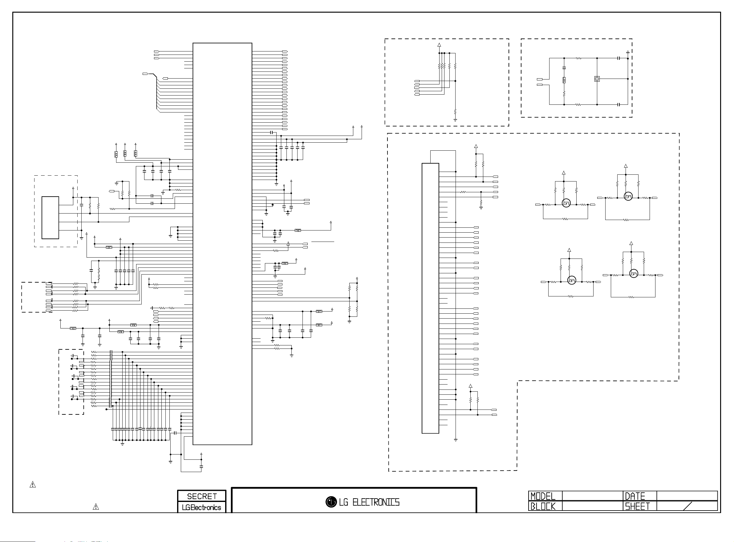
USB HUB
Copyright © 2010 LG Electronics Inc. All rights reserved.
Only for training and service purposes
LGE Internal Use Only
USB2_DM_to_MAIN
USB2_DP_to_MAIN
USB1_DM_to_MAIN
USB1_DP_to_MAIN
USB_DM
USB_DP
BROAD BAND STUDIO
FOR DEBUG
P200
TJC2508-4A
1
2
3
4
BT_DM
BT_DP
A2.5V
COMP_L_IN
COMP_R_IN
SC1_L_IN
SC1_R_IN
SIDE_LIN
SIDE_RIN
PC_L_IN
PC_R_IN
AUDIO INCM-TP
PLACE NEAR JACKS
CI_OUTCLK,CI_OUTDATA[0-7],CI_OUTSTART,CI_OUTVALID
L202
BLM18PG121SN1D
+3.3V_MULTI
BLM18PG121SN1D
TP201
TP200
TP204
TP203
TP202
0USE_USB_HUB
0USE_USB_HUB
0USE_NO_HUB
0USE_USB_HUB
0USE_USB_HUB
0USE_NO_HUB
0USE_NO_HUB
L200
C200
R2020USE_NO_HUB
R203
R204
R205
R206
R207
R200
R201
4.7uF
DTV/MNT_V_OUT
R208
1.5K
A3.3V
C202
100pF
C201
4.7uF
R220 51
R221 51
R222 5.1
R209 51
R210 51
R211 5.1
R212 51
R213 51
R223 5.1
R214 51
R215 51
R224 5.1
R216 51
R217 51
R218 5.1
R219 51
R226
1.5K
R229 0
A1.2V
L201
BLM18PG121SN1D
R227
3.9K
R228
120
A1.2V
C203
0.1uF
16V
C213 0.015uF
C214 0.015uF
C215 0.15uF
C206 0.015uF
C220 0.015uF
C222 0.15uF
C207 0.015uF
C208 0.015uF
C225 0.15uF
C209 0.015uF
C210 0.015uF
C227 0.15uF
C211 0.015uF
C212 0.015uF
C216 0.15uF
C204 0.015uF
C205 0.015uF
R225
51
READY
BLM18PG121SN1D
50V
25V
25V
25V
25V
C217 0.047uF
FE_TS_DATA_CLK
FE_TS_SERIAL
FE_TS_SYNC
A2.5V
A1.2V
A3.3V
L211
L210
BLM18PG121SN1D
BLM18PG121SN1D
4.7uF
C231
R220 : BCM recommened resistor 562 ohm
75
R231
A2.5V
C223 4.7uF
C22 1 0.1u F
C21 9 0 .1uF
C21 8 0 .1uF
BLM18PG121SN1D
L204
L203
C224
0.1uF
0.047uF
C229 0.047uF
C232 0.047uF
C235
C238 0.47uF
C230 0.47uF
READY
READY
READY
READY
75
R233
READY
C22 6 0.1u F
C228
4.7uF
C240 0.047uF
C242 0.047uF
EPHY_RDN
EPHY_RDP
EPHY_TDN
EPHY_TDP
C244 0.47uF
C265 0.047uF
C237
C233
0.01uF
D3.3V
0.1uF
C234
C266 0.047uF
0.1uF
0.1uF
C268 0.047uF
C267 0.47uF
C236
4.7uF
C239
C269 0.047uF
2.7K
R235
2.7K
CI_OUTDATA[0]
CI_OUTDATA[1]
CI_OUTDATA[2]
CI_OUTDATA[3]
CI_OUTDATA[4]
CI_OUTDATA[5]
CI_OUTDATA[6]
CI_OUTDATA[7]
CI_OUTSTART
CI_OUTVALID
0.1uF
C241
R285
R236
240
C271 0.047uF
C270 0.47uF
CI_A[14]
0.1uF
C243
R238 560
1K
R237
C273
0.1uF
C272 0.047uF
LGE3556C (C0 VERSION)
D23
PKT0_CLK
C24
PKT0_DATA
B26
PKT0_SYNC
A25
RMX0_CLK
B25
RMX0_DATA
A26
RMX0_SYNC
G23
POD2CHIP_MCLKI
D25
POD2CHIP_MDI0
D24
POD2CHIP_MDI1
C25
POD2CHIP_MDI2
E27
POD2CHIP_MDI3
E26
POD2CHIP_MDI4
D28
POD2CHIP_MDI5
D27
POD2CHIP_MDI6
D26
POD2CHIP_MDI7
E23
POD2CHIP_MISTRT
E24
POD2CHIP_MIVAL
F25
CHIP2POD_MCLKO
C27
CHIP2POD_MDO0
C26
CHIP2POD_MDO1
B28
CHIP2POD_MDO2
B27
CHIP2POD_MDO3
A27
CHIP2POD_MDO4
F24
CHIP2POD_MDO5
F23
CHIP2POD_MDO6
E25
CHIP2POD_MDO7
C28
CHIP2POD_MOSTRT
A28
CHIP2POD_MOVAL
AC18
VDAC_AVDD2P5
AF20
VDAC_AVDD1P2
AG20
VDAC_AVDD3P3_1
AG21
VDAC_AVDD3P3_2
AF19
VDAC_AVSS_1
AD20
VDAC_AVSS_2
AE20
VDAC_AVSS_3
AH22
VDAC_RBIAS
AH20
VDAC_1
AG19
VDAC_2
AH21
VDAC_VREG
M25
BSC_S_SCL
M24
BSC_S_SDA
R6
USB_AVSS_1
T6
USB_AVSS_2
R7
USB_AVSS_3
T7
USB_AVSS_4
T8
USB_AVSS_5
R3
USB_AVDD1P2
U3
USB_AVDD1P2PLL
T4
USB_AVDD2P5
T3
USB_AVDD2P5REF
R4
USB_AVDD3P3
U4
USB_RREF
V1
USB_DM1
V2
USB_DP1
U1
USB_DM2
U2
USB_DP2
T5
USB_MONCDR
R5
USB_MONPLL
R1
USB_PWRFLT_1
R2
USB_PWRFLT_2
T2
USB_PWRON_1
T1
USB_PWRON_2
P6
EPHY_VREF
P5
EPHY_RDAC
P3
EPHY_RDN
P2
EPHY_RDP
N3
EPHY_TDN
N2
EPHY_TDP
P1
EPHY_AVDD1P2
P4
EPHY_AVDD2P5
N4
EPHY_PLL_VDD1P2
N1
EPHY_AGND_1
N5
EPHY_AGND_2
P7
EPHY_AGND_3
AE6
AUDMX_LEFT1
AD7
AUDMX_RIGHT1
AF6
AUDMX_INCM1
AH4
AUDMX_LEFT2
AG5
AUDMX_RIGHT2
AG4
AUDMX_INCM2
AG6
AUDMX_LEFT3
AF7
AUDMX_RIGHT3
AE7
AUDMX_INCM3
AH5
AUDMX_LEFT4
AG7
AUDMX_RIGHT4
AH6
AUDMX_INCM4
AD8
AUDMX_LEFT5
AF8
AUDMX_RIGHT5
AE8
AUDMX_INCM5
AH7
AUDMX_LEFT6
AH8
AUDMX_RIGHT6
AG8
AUDMX_INCM6
AF5
AUDMX_AVSS_1
AB9
AUDMX_AVSS_2
AA10
AUDMX_AVSS_3
AB10
AUDMX_AVSS_4
AA11
AUDMX_AVSS_5
AB11
AUDMX_AVSS_6
AC8
AUDMX_LDO_CAP
AE5
AUDMX_AVDD2P5
IC100
VCXO_PLL_AUDIO_TESTOUT
PLL_MAIN_MIPS_EREF_TESTOUT
A2.5V
LVDS_TX_0_DATA0_P
LVDS_TX_0_DATA0_N
LVDS_TX_0_DATA1_P
LVDS_TX_0_DATA1_N
LVDS_TX_0_DATA2_P
LVDS_TX_0_DATA2_N
LVDS_TX_0_DATA3_P
LVDS_TX_0_DATA3_N
LVDS_TX_0_DATA4_P
LVDS_TX_0_DATA4_N
LVDS_TX_0_CLK_P
LVDS_TX_0_CLK_N
LVDS_TX_1_DATA0_P
LVDS_TX_1_DATA0_N
LVDS_TX_1_DATA1_P
LVDS_TX_1_DATA1_N
LVDS_TX_1_DATA2_P
LVDS_TX_1_DATA2_N
LVDS_TX_1_DATA3_P
LVDS_TX_1_DATA3_N
LVDS_TX_1_DATA4_P
LVDS_TX_1_DATA4_N
LVDS_TX_1_CLK_P
LVDS_TX_1_CLK_N
LVDS_PLL_VREG
LVDS_TX_AVDDC1P2
LVDS_TX_AVDD2P5_1
LVDS_TX_AVDD2P5_2
LVDS_TX_AVSS_1
LVDS_TX_AVSS_2
LVDS_TX_AVSS_3
LVDS_TX_AVSS_4
LVDS_TX_AVSS_5
LVDS_TX_AVSS_6
LVDS_TX_AVSS_7
LVDS_TX_AVSS_8
LVDS_TX_AVSS_9
LVDS_TX_AVSS_10
LVDS_TX_AVSS_11
CLK54_AVDD1P2
CLK54_AVDD2P5
CLK54_AVSS
CLK54_XTAL_N
CLK54_XTAL_P
CLK54_MONITOR
PM_OVERRIDE
VCXO_AGND_1
VCXO_AGND_2
VCXO_AGND_3
VCXO_AVDD1P2
RESET_OUTB
RESETB
NMIB
TMODE_0
TMODE_1
TMODE_2
TMODE_3
SPI_S_MISO
POR_OTP_VDD2P5
POR_VDD1P2
EJTAG_TCK
EJTAG_TDI
EJTAG_TDO
EJTAG_TMS
EJTAG_TRSTB
EJTAG_CE0
EJTAG_CE1
PLL_MAIN_AVDD1P2
PLL_MAIN_AGND
PLL_RAP_AVD_TESTOUT
PLL_RAP_AVD_AVDD1P2
PLL_RAP_AVD_AGND
BYP_CPU_CLK
BYP_DS_CLK
BYP_SYS216_CLK
BYP_SYS175_CLK
B4
A4
C6
B6
B3
A3
A1
A2
D5
D6
C5
B5
B1
B2
C2
C3
D1
D2
E1
E2
E3
E4
D3
D4
F5
F1
F4
F2
C1
F3
C4
A5
E5
E6
D7
E7
F7
G7
H7
AD27
AD28
AD26
AC26
AC27
AE25
Y23
AA23
AB24
AC24
AF25
AF24
P24
F6
N24
J5
J4
J6
J3
V25
AH3
AB8
H4
H3
H2
H1
G1
H6
H5
AB26
AC25
AB27
M6
N6
N7
AA24
Y24
AE24
AD25
C246
10uF
C247
0.1uF
C248
R239
READY
READY
4.7K
R240
BLM18PG121SN1D
10uF
390
C25 2
A1.2V
C25 3
C249
0.1uF
C25 1
R2411K
R2421K
0.1 uF
C25 4
0.1 uF
C250
4.7uF
D3.3V
L205
JTAG_TCLK
JTAG_TDI
JTAG_TDO
JTAG_TMS
/JTAG_TRST
0.1 uF
LVDS_TX_0_DATA0_P
LVDS_TX_0_DATA0_N
LVDS_TX_0_DATA1_P
LVDS_TX_0_DATA1_N
LVDS_TX_0_DATA2_P
LVDS_TX_0_DATA2_N
LVDS_TX_0_DATA3_P
LVDS_TX_0_DATA3_N
LVDS_TX_0_DATA4_P
LVDS_TX_0_DATA4_N
LVDS_TX_0_CLK_P
LVDS_TX_0_CLK_N
LVDS_TX_1_DATA0_P
LVDS_TX_1_DATA0_N
LVDS_TX_1_DATA1_P
LVDS_TX_1_DATA1_N
LVDS_TX_1_DATA2_P
LVDS_TX_1_DATA2_N
LVDS_TX_1_DATA3_P
LVDS_TX_1_DATA3_N
LVDS_TX_1_DATA4_P
LVDS_TX_1_DATA4_N
LVDS_TX_1_CLK_P
LVDS_TX_1_CLK_N
0.1 uF
0.1 uF
4.7uF
C257
C260
C25 8
A2.5V
0.1 uF
C25 6
L206
BLM18PG121SN1D
A2.5V
A1.2V
C25 9
C255
4.7uF
4.7uF
54MHz_XTAL_N
54MHz_XTAL_P
WATCH_DOG_RESET
SOC_RESET
L207
BLM18PG121SN1D
L208
BLM18PG121SN1D
C261
0.1 uF
4.7uF
A1.2V
007:B7
007:B7
A1.2V
A1.2V
008:I1
008:I2
READY
R243
2.7K
R244
2.7K
A1.2V
D3.3V
A2.5V
READY
R245
2.7K
R246
2.7K
EJTAG
002:D4
002:D4
002:D4
002:D4
002:D4
LVDS
/JTAG_TRST
JTAG_TDI
JTAG_TDO
JTAG_TMS
JTAG_TCLK
D3.3V
52
FHD
TF05-51S
P201
54MHz X-TAL
1K
1K
1K
1K
1K
READY
READY
R279
R275
R277
R276
R278
1K
R281
+3.3V_MULTI
R230
4.7K
R232
R253100
FHD
R234
4.7K
4.7K
R255
27K
LVDS_TX_1_DATA4_N
LVDS_TX_1_DATA4_P
LVDS_TX_1_DATA3_N
LVDS_TX_1_DATA3_P
LVDS_TX_1_DATA2_N
LVDS_TX_1_DATA2_P
LVDS_TX_1_CLK_N
LVDS_TX_1_CLK_P
LVDS_TX_1_DATA1_N
LVDS_TX_1_DATA1_P
LVDS_TX_1_DATA0_N
LVDS_TX_1_DATA0_P
LVDS_TX_0_DATA4_N
LVDS_TX_0_DATA4_P
LVDS_TX_0_DATA3_N
LVDS_TX_0_DATA3_P
LVDS_TX_0_DATA2_N
LVDS_TX_0_DATA2_P
LVDS_TX_0_CLK_N
LVDS_TX_0_CLK_P
LVDS_TX_0_DATA1_N
LVDS_TX_0_DATA1_P
LVDS_TX_0_DATA0_N
LVDS_TX_0_DATA0_P
R250
4.7K
PC_SER_CLK
PC_SER_DATA
MDL_SCL
DISP_EN
MDL_SDA
MOD_ROM_TX_MOD
MOD_ROM_RX_MOD
51
50
49
48
FHD
47
46
45
44
43
42
41
40
39
38
37
36
35
34
33
32
31
30
29
28
27
26
25
24
23
22
21
20
19
18
17
16
15
14
13
12
11
10
9
8
7
6
5
4
3
2
1
+3.3V_MULTI
005:B6
005:B6
54MHz_XTAL_N
54MHz_XTAL_P
SCL3_3.3V
MOD_ROM_RX
22
READY
R258
+3.3V_MULTI
R260
4.7K
READY
READY
R256
22
C262
L209
R247
READY
R261
+3.3V_MULTI
READY
R257
4.7K
CASE 1 : R = 0 ohm --> CL = 8 pF
CASE 2 : R = 22 Ohm --> CL = 22pF
22
R249
33pF
1008LS-272XJLC
604
22
R248
READY
R262
4.7K
0
G
SDA3_3.3V
005:B6
D
S
R263
22
Q200
READY
2N7002(F)
READY
R28322
READY
R269
4.7K
READY
R268
0
G
MOD_ROM_TX
005:B6
D
S
R270
22
Q202
READY
2N7002(F)
READY
R25922
X200
21
54MHz
MDL_SCL
3
R265
READY
READY
R264
22
002:G4
R272
22
MOD_ROM_RX_MOD
002:G4
C263
12pF
12pF
C264
+3.3V_MULTI
4.7K
READY
R266
2N7002(F)
+3.3V_MULTI
READY
R273
4.7K
READY
0
S
Q201
READY
READY
R267
READY
G
D
R28422
R286
0
G
S
Q203
2N7002(F)
READY
R27422
4.7K
READY
R287
D
READY
R271
22
4.7K
READY
R288
22
MDL_SDA
MOD_ROM_TX_MOD
002:G4
002:G4
THE SYMBOL MARK OF THIS SCHEMETIC DIAGRAM INCORPORATES
SPECIAL FEATURES IMPORTANT FOR PROTECTION FROM X-RADIATION.
FILRE AND ELECTRICAL SHOCK HAZARDS, WHEN SERVICING IF IS
ESSENTIAL THAT ONLY MANUFATURES SPECFIED PARTS BE USED FOR
THE CRITICAL COMPONENTS IN THE SYMBOL MARK OF THE SCHEMETIC.
C245
10uF
BCM3556-C0
BCM AUDIO/LVDS
10/01/
2 13
Page 14
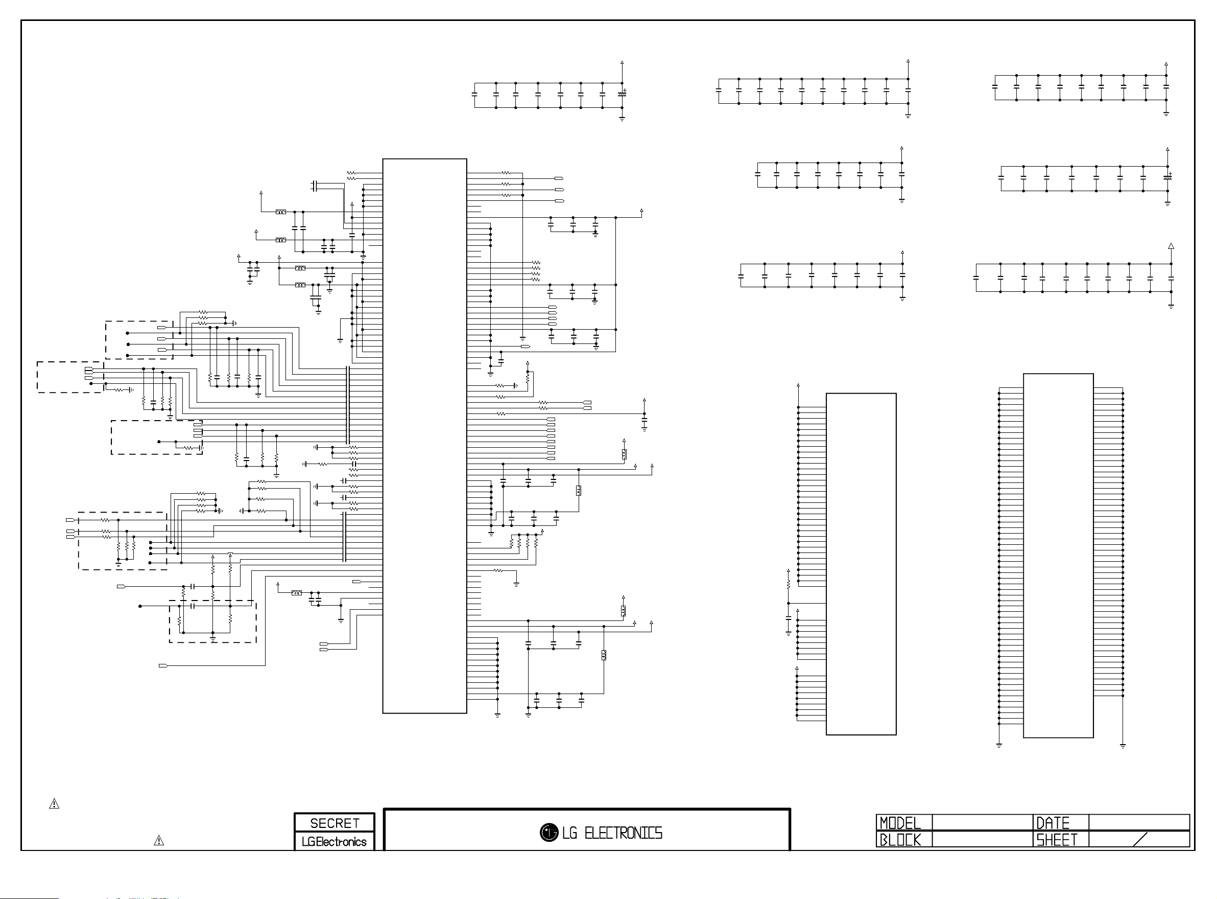
D1.2V
Copyright © 2010 LG Electronics Inc. All rights reserved.
Only for training and service purposes
LGE Internal Use Only
D1.2V
D3.3V
COMPONENT
COMP_Y
COMP_Pr
COMP_Pb
COMP INCM-TP
PLACE NEAR JACKS
TU_CVBS
SC1_CVBS_IN
AV_CVBS_IN
DSUB RGB INCM-TP
PLACE NEAR JACKS
R300
CVBS INCM-TP
PLACE NEAR JACKS
CVBS
R308
R309
R359
TU_SIF
DSUB
009:G4
009:G4
009:G5
R360
75
DSUB_R
DSUB_G
DSUB_B
34
75
R301
SC RGB INCM-TP
PLACE NEAR JACKS
18
12
12
R364
62
R362
62
GND
SC1_FB
75
75
10pF
C300
R305
R303
READY
SC1_G
SC1_R
SC1_B
R307
SC1_RGB
R306
240
R304
120
CONNECT NEAR BCM CHIP
R314
R311
R312
R313
R310
R315
R316
0.1uF
C301
C302
0.1uF
C3059
C3057
10uF
0.1uF
D1.8V
C3056
C3060
4.7uF
33uF
D1.8V
C3061
0.1uF
16V
16V
16V
C3050
4.7uF
C3051
1000pF
C3055
0.1uF
C3054
0.01uF
C3053
4.7uF
C3058
0.1uF
16V
C3036
C3039
C3042
C3045
0.1uF
C3047
0.1uF
C3049
0.1uF
16V
DVSS_62
DVSS_63
DVSS_64
DVSS_65
DVSS_66
DVSS_67
DVSS_68
DVSS_69
DVSS_70
DVSS_71
DVSS_72
DVSS_73
DVSS_74
DVSS_75
DVSS_76
DVSS_77
DVSS_78
DVSS_79
DVSS_80
DVSS_81
DVSS_82
DVSS_83
DVSS_84
DVSS_85
DVSS_86
DVSS_87
DVSS_88
DVSS_89
DVSS_90
DVSS_91
DVSS_92
DVSS_93
DVSS_94
DVSS_95
DVSS_96
DVSS_97
DVSS_98
DVSS_99
DVSS_100
DVSS_101
DVSS_102
DVSS_103
DVSS_104
DVSS_105
DVSS_106
DVSS_107
DVSS_108
DVSS_109
DVSS_110
DVSS_111
DVSS_112
DVSS_113
DVSS_114
DVSS_115
DVSS_116
DVSS_117
C3048
4.7uF
C3052
0.1uF
P16
R16
T16
U16
V16
AA16
D17
L17
M17
N17
P17
R17
T17
U17
V17
AA17
AC19
G18
L18
M18
N18
P18
R18
T18
U18
V18
D20
G20
H20
A21
E21
F21
G21
E22
F22
G22
H22
J22
K22
L22
M22
N22
P22
R22
T22
U22
V22
W22
Y22
AA22
W23
AB23
F28
M28
T28
AC28
R363
C3016
4.7uF
C3015
1000pF
A3.3V
20
C3019
C3022
1000pF
0.01uF
C3018
C3021
0.01uF
0.1uF
C3020
C3017
1000pF
1000pF
D1.2V
LGE3556C (C0 VERSION)
H8
VDDC_1
J8
VDDC_2
K8
VDDC_3
L8
VDDC_4
M8
VDDC_5
N8
VDDC_6
P8
VDDC_7
R8
VDDC_8
AA8
VDDC_9
H9
VDDC_10
H10
VDDC_11
H11
VDDC_12
H12
VDDC_13
H13
VDDC_14
H14
VDDC_15
H15
VDDC_16
H16
VDDC_17
H17
VDDC_18
H18
VDDC_19
H19
VDDC_20
H21
VDDC_21
J21
VDDC_22
K21
VDDC_23
L21
VDDC_24
M21
VDDC_25
N21
VDDC_26
P21
VDDC_27
R21
VDDC_28
T21
VDDC_29
U21
VDDC_30
V21
VDDC_31
W21
VDDC_32
Y21
VDDC_33
AH27
AA12
AA13
AA18
AA19
AB28
AGC_VDDO
VDDO_1
VDDO_2
VDDO_3
VDDO_4
E28
VDDO_5
L28
VDDO_6
U28
VDDO_7
VDDO_8
A9
DDRV_1
G9
DDRV_2
G11
DDRV_3
G13
DDRV_4
A14
DDRV_5
G15
DDRV_6
G17
DDRV_7
A19
DDRV_8
G19
DDRV_9
D3.3V
D1.8V
C3001
C3000
4.7uF
0.1uF
LGE3556C (C0 VERSION)
READY
R332 0
R333 0
READY
A2.5V
BLM18PG121SN1D
L300
C309
A1.2V
0.1uF
L301
BLM18PG121SN1D
A1.2V
C306
0.1uF
34
34
34
READY
READY
75
75
R317
C304 10pF
C303 10pF
R320
34
34
34
34
34
A2.5V
R318
10K
R319
12K
A2.5V
10K
75
R32 3
R321
12K
R322
R324 75
C305
R326
C307
0.1uF
READY
10pF
C308
75
READY
10pF
R32 5
READY
R329 75
READY
R327
A2.5V
75
R33 0
75
R328
READY
75
READY
75
A1.2V
BLM18PG121SN1D
BLM18PG121SN1D
C3150.01uF
C3160.01uF
READY
C310
4.7uF
C317
0.1uF
C318
L303
1000pF
L304
C312
1000pF
READY
R331 34
READY
L302
BLM18PG121SN1D
C311
0.1uF
RGB_HSYNC
RGB_VSYNC
C347
0.1uF
C319
4.7uF
C320
0.01uF
C313
0.01uF
C332
C333
C334
C335
C336
C337
C338
C339
C340
C341
C342
C343
C344
C345
READY
READY
READY
C346 0.1uF
READY
READY
READY
C321 0.1uF
READY
READY
C322 0.1uF
READY
READY
C323
C324
C325
C326
C327
C328
C329
C330
C331
SC1_ID
C314
4.7uF
READY
A1.2V
0
0
0
0
0
0
0
0
0
0.1uF
0.1uF
0.1uF
0.1uF
0.1uF
0.1uF
0.1uF
0.1uF
0.1uF
0.1uF
0.1uF
0.1uF
0.1uF
0.1uF
0.1uF
0.1uF
0.1uF
0.1uF
0.1uF
0.1uF
0.1uF
0.1uF
0.1uF
R334
R335
R336
R337
R338
R339
R340
R341
R342
AG28
DS_AGCI_CTL
AH28
DS_AGCT_CTL
AA21
EDSAFE_AVSS_1
AB22
EDSAFE_AVSS_2
AF26
EDSAFE_AVSS_3
AF27
EDSAFE_AVSS_4
AF28
EDSAFE_AVSS_5
AG27
EDSAFE_AVDD2P5
AE26
EDSAFE_DVDD1P2
AE28
EDSAFE_IF_N
AE27
EDSAFE_IF_P
AD24
PLL_DS_AGND
AB19
PLL_DS_AVDD1P2
AB25
PLL_DS_TESTOUT
AB18
SD_V5_AVDD1P2
AC17
SD_V5_AVDD2P5
AB17
SD_V5_AVSS
AD14
SD_V1_AVDD1P2
AD16
SD_V1_AVDD2P5
AB15
SD_V1_AVSS_1
AC15
SD_V1_AVSS_2
AD13
SD_V2_AVDD1P2
AE13
SD_V2_AVDD2P5
AC13
SD_V2_AVSS_1
AB14
SD_V2_AVSS_2
AC14
SD_V2_AVSS_3
AC12
SD_V3_AVDD1P2
AD12
SD_V3_AVDD2P5
AB13
SD_V3_AVSS_1
AA14
SD_V3_AVSS_2
AC11
SD_V4_AVDD1P2
AD11
SD_V4_AVDD2P5
AB12
SD_V4_AVSS
AD10
SD_R
AC10
SD_INCM_R
AE9
SD_G
AF9
SD_INCM_G
AH9
SD_B
AG9
SD_INCM_B
AG15
SD_Y1
AE15
SD_PR1
AF15
SD_PB1
AH15
SD_INCM_COMP1
AG16
SD_Y2
AF16
SD_PR2
AH17
SD_PB2
AH16
SD_INCM_COMP2
AG14
SD_Y3
AE14
SD_PR3
AF14
SD_PB3
AH14
SD_INCM_COMP3
AH10
SD_L1
AG10
SD_C1
AE10
SD_INCM_LC1
AE11
SD_L2
AF11
SD_C2
AH11
SD_INCM_LC2
AH13
SD_L3
AE12
SD_C3
AF12
SD_INCM_LC3
AD9
SD_CVBS1
AG11
SD_CVBS2
AG12
SD_CVBS3
AF13
SD_CVBS4
AC9
SD_INCM_CVBS1
AF10
SD_INCM_CVBS2
AH12
SD_INCM_CVBS3
AG13
SD_INCM_CVBS4
AF17
SD_SIF1
AG17
SD_INCM_SIF1
AD15
SD_FB
AE16
SD_FS
AE17
SD_FS2
AB16
PLL_VAFE_AVDD1P2
AA15
PLL_VAFE_AVSS
AC16
PLL_VAFE_TESTOUT
AG3
RGB_HSYNC
AF4
RGB_VSYNC
IC100
I2S_CLK_IN
I2S_CLK_OUT
I2S_DATA_IN
I2S_DATA_OUT
I2S_LR_IN
I2S_LR_OUT
AUD_LEFT0_N
AUD_LEFT0_P
AUD_AVDD2P5_0
AUD_AVSS_0_1
AUD_AVSS_0_2
AUD_AVSS_0_3
AUD_AVSS_0_4
AUD_AVSS_0_5
AUD_RIGHT0_N
AUD_RIGHT0_P
AUD_LEFT1_N
AUD_LEFT1_P
AUD_RIGHT1_N
AUD_RIGHT1_P
AUD_AVDD2P5_1
AUD_AVSS_1_1
AUD_AVSS_1_2
AUD_AVSS_1_3
AUD_LEFT2_N
AUD_LEFT2_P
AUD_RIGHT2_N
AUD_RIGHT2_P
AUD_AVDD2P5_2
AUD_AVSS_2_1
AUD_AVSS_2_2
AUD_SPDIF
SPDIF_AVDD2P5
SPDIF_AVSS
SPDIF_IN_N
SPDIF_IN_P
HDMI_RX_0_CEC_DAT
HDMI_RX_0_HTPLG_IN
HDMI_RX_0_HTPLG_OUT
HDMI_RX_0_DDC_SCL
HDMI_RX_0_DDC_SDA
HDMI_RX_0_RESREF
HDMI_RX_0_CLK_N
HDMI_RX_0_CLK_P
HDMI_RX_0_DATA0_N
HDMI_RX_0_DATA0_P
HDMI_RX_0_DATA1_N
HDMI_RX_0_DATA1_P
HDMI_RX_0_DATA2_N
HDMI_RX_0_DATA2_P
HDMI_RX_0_VDD3P3
HDMI_RX_0_VDD1P2
HDMI_RX_0_VDD2P5
HDMI_RX_0_AVSS_1
HDMI_RX_0_AVSS_2
HDMI_RX_0_AVSS_3
HDMI_RX_0_AVSS_4
HDMI_RX_0_AVSS_5
HDMI_RX_0_AVSS_6
HDMI_RX_0_PLL_AVSS
HDMI_RX_0_PLL_DVDD1P2
HDMI_RX_0_PLL_DVSS
HDMI_RX_1_CEC_DAT
HDMI_RX_1_HTPLG_IN
HDMI_RX_1_HTPLG_OUT
HDMI_RX_1_DDC_SCL
HDMI_RX_1_DDC_SDA
HDMI_RX_1_RESREF
HDMI_RX_1_CLK_N
HDMI_RX_1_CLK_P
HDMI_RX_1_DATA0_N
HDMI_RX_1_DATA0_P
HDMI_RX_1_DATA1_N
HDMI_RX_1_DATA1_P
HDMI_RX_1_DATA2_N
HDMI_RX_1_DATA2_P
HDMI_RX_1_VDD3P3
HDMI_RX_1_VDD1P2
HDMI_RX_1_VDD2P5
HDMI_RX_1_AVSS_1
HDMI_RX_1_AVSS_2
HDMI_RX_1_AVSS_3
HDMI_RX_1_AVSS_4
HDMI_RX_1_AVSS_5
HDMI_RX_1_AVSS_6
HDMI_RX_1_AVSS_7
HDMI_RX_1_AVSS_8
HDMI_RX_1_AVSS_9
HDMI_RX_1_PLL_AVSS
HDMI_RX_1_PLL_DVDD1P2
HDMI_RX_1_PLL_DVSS
AE18
AF18
AD17
AH19
AD18
AG18
AG26
AH26
AF23
AA20
AB21
AC22
AC23
AD23
AH25
AG25
AH23
AG23
AG24
AH24
AE22
AB20
AC21
AE23
AF21
AE21
AF22
AG22
AD21
AC20
AD22
AH2
AC6
AE4
AF3
AH1
AG1
AA6
AA5
AB3
Y6
AC4
AC1
AC2
AD1
AD2
AE1
AE2
AF1
AF2
AD3
AE3
AC3
AD4
AB5
AB6
AG2
AB4
AA7
Y8
AC5
W8
AA3
V4
U6
V5
V3
W4
W2
W3
Y1
Y2
AA2
AA1
AB2
AB1
Y3
Y4
W5
W1
U5
W6
U7
V7
W7
U8
V8
Y5
V6
AA4
Y7
R347 0
READY
R348 0
READY
R349
READY
C350
0.1uF
R344
1K
R345
10K
R346499
R350
R343499
READY
C351
4.7uF
10K
C3002
1000pF
0
READY
R365 0
READY
R366 0
READY
R357 0
READY
R358 0
+5V_MULTI
R352
0
C352
1000pF
R351 10K
R353 10K
C3003
0.01uF
SPDIF_OUT
C354
0.1uF
C356
0.01uF
10K
R354
C355
4.7uF
C357
1000pF
R35522
R35622
D3.3V
C3004
0.1uF
AUD_SCK
AUD_LRCH
AUD_LRCK
C360
C368
0.01uF
0.1uF
C367
C359
0.1uF
0.01uF
SCART1_Lout_N
SCART1_Lout_P
SCART1_Rout_N
SCART1_Rout_P
C369
C361
0.1uF
0.01uF
009:D6
HDMI0_RXC-_BCM
HDMI0_RXC+_BCM
HDMI0_RX0-_BCM
HDMI0_RX0+_BCM
HDMI0_RX1-_BCM
HDMI0_RX1+_BCM
HDMI0_RX2-_BCM
HDMI0_RX2+_BCM
C362
0.1uF
C364
10uF
C363
0.1uF
C365
0.01uF
C3005
C3006
10uF
10uF
C374
10uF
C373
10uF
C375
10uF
HDMI_SCL
HDMI_SDA
008:AA19
008:AB19
008:AB19
008:AB19
008:AC19
008:AC19
008:AC19
008:AD19
BLM18PG121SN1D
L305
C370
0.1uF
C372
10uF
C3007
33uF
008:AA19
008:AA19
A3.3V
BLM18PG121SN1D
L308
A1.2V
A3.3V
BLM18PG121SN1D
L307
A1.2V
BLM18PG121SN1D
L306
A2.5V
A2.5V
C378
0.1uF
16V
A2.5V
A2.5V
C3009
1000pF
C3010
0.01uF
C3011
1000pF
C3013
0.1uF
C3012
0.1uF
C3014
1000pF
C389
0.1uF
C3024
4.7uF
C3023
0.01uF
C3025
0.1uF
IC100
C3027
1000pF
C3026
0.01uF
C3028
4.7uF
C3031
1000pF
C3030
0.01uF
C3029
0.01uF
D3.3V
D1.8V
C3032
0.1uF
C3033
0.01uF
C3034
0.01uF
C3035
0.1uF
4.7uF
1000pF
0.01uF
C3040
C3038
0.1uF
C3041
C3037
0.1uF
0.1uF
16V
16V
16V
LGE3556C (C0 VERSION)
AD5
AD6
J7
K7
L7
M7
AB7
AC7
G8
D9
AA9
G10
A11
L11
M11
N11
P11
R11
T11
U11
V11
D12
G12
L12
M12
N12
P12
R12
T12
U12
V12
L13
M13
N13
P13
R13
T13
U13
V13
G14
L14
M14
N14
P14
R14
T14
U14
V14
L15
M15
N15
P15
R15
T15
U15
V15
A16
G16
L16
M16
N16
0.1uF
C3043
10uF
10V
DVSS_1
DVSS_2
DVSS_3
DVSS_4
DVSS_5
DVSS_6
DVSS_7
DVSS_8
DVSS_9
DVSS_10
DVSS_11
DVSS_12
DVSS_13
DVSS_14
DVSS_15
DVSS_16
DVSS_17
DVSS_18
DVSS_19
DVSS_20
DVSS_21
DVSS_22
DVSS_23
DVSS_24
DVSS_25
DVSS_26
DVSS_27
DVSS_28
DVSS_29
DVSS_30
DVSS_31
DVSS_32
DVSS_33
DVSS_34
DVSS_35
DVSS_36
DVSS_37
DVSS_38
DVSS_39
DVSS_40
DVSS_41
DVSS_42
DVSS_43
DVSS_44
DVSS_45
DVSS_46
DVSS_47
DVSS_48
DVSS_49
DVSS_50
DVSS_51
DVSS_52
DVSS_53
DVSS_54
DVSS_55
DVSS_56
DVSS_57
DVSS_58
DVSS_59
DVSS_60
DVSS_61
C3044
0.1uF
C3046
0.1uF
16V
IC100
THE SYMBOL MARK OF THIS SCHEMETIC DIAGRAM INCORPORATES
SPECIAL FEATURES IMPORTANT FOR PROTECTION FROM X-RADIATION.
FILRE AND ELECTRICAL SHOCK HAZARDS, WHEN SERVICING IF IS
ESSENTIAL THAT ONLY MANUFATURES SPECFIED PARTS BE USED FOR
THE CRITICAL COMPONENTS IN THE SYMBOL MARK OF THE SCHEMETIC.
BCM3556-C0
10/01/
BCM VIDEO IN/BCM POWER 3 13
Page 15
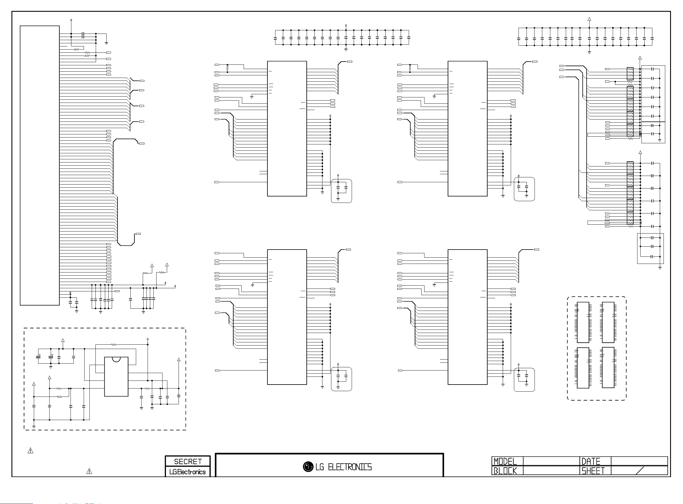
LGE3556C (C0 VERSION)
Copyright © 2010 LG Electronics Inc. All rights reserved.
Only for training and service purposes
LGE Internal Use Only
IC100
DDR_PLL_TEST
DDR_VDDP1P8_1
DDR_VDDP1P8_2
DDR_BVDD0
DDR_BVDD1
DDR_BVSS0
DDR_BVSS1
DDR_PLL_LDO
DDR01_CKE
DDR_COMP
DDR01_ODT
DDR_EXT_CLK
DDR0_CLK
DDR0_CLKB
DDR1_CLK
DDR1_CLKB
DDR01_A00
DDR01_A01
DDR01_A02
DDR01_A03
DDR0_A04
DDR0_A05
DDR0_A06
DDR01_A07
DDR01_A08
DDR01_A09
DDR01_A10
DDR01_A11
DDR01_A12
DDR01_A13
DDR1_A04
DDR1_A05
DDR1_A06
DDR01_BA0
DDR01_BA1
DDR01_BA2
DDR01_CASB
DDR0_DQ00
DDR0_DQ01
DDR0_DQ02
DDR0_DQ03
DDR0_DQ04
DDR0_DQ05
DDR0_DQ06
DDR0_DQ07
DDR0_DQ08
DDR0_DQ09
DDR0_DQ10
DDR0_DQ11
DDR0_DQ12
DDR0_DQ13
DDR0_DQ14
DDR0_DQ15
DDR1_DQ00
DDR1_DQ01
DDR1_DQ02
DDR1_DQ03
DDR1_DQ04
DDR1_DQ05
DDR1_DQ06
DDR1_DQ07
DDR1_DQ08
DDR1_DQ09
DDR1_DQ10
DDR1_DQ11
DDR1_DQ12
DDR1_DQ13
DDR1_DQ14
DDR1_DQ15
DDR0_DM0
DDR0_DM1
DDR1_DM0
DDR1_DM1
DDR0_DQS0
DDR0_DQS0B
DDR0_DQS1
DDR0_DQS1B
DDR1_DQS0
DDR1_DQS0B
DDR1_DQS1
DDR1_DQS1B
DDR01_RASB
DDR_VREF0
DDR_VREF1
DDR01_WEB
* DDR_VTT
C402
C485
100uF
100uF
16V
16V
DDR1_VREF0
DDR0_VREF0
C400
0.1uF
16V
DDR_VTT
C401
0.1uF
16V
R400
0
R401
0
A6
A24
B7
B24
F20
B23
B17
C22
E16
C23
B12
C12
A13
A12
B15
E14
A15
D15
E13
E12
F13
C14
F14
B14
D14
C13
D13
B13
F15
C15
D16
F16
B16
E15
A17
A8
B11
B8
D11
E11
C8
C11
C9
D8
E10
E9
F11
F12
E8
D10
F8
C18
C20
A18
B21
C21
B18
B20
D18
E18
D21
F18
E20
A22
F17
B22
E17
A10
C10
A20
F19
B10
B9
F10
F9
B19
C19
E19
D19
C16
A7
A23
C17
C7
D22
0.1uF
C403
10uF
10V
C404
A1.2V
C4080.1uF
C4090.1uF
R403 0
READY
R404 0
R406 240
1%
DDR01_A[0]
DDR01_A[1]
DDR01_A[2]
DDR01_A[3]
DDR0_A[4]
DDR0_A[5]
DDR0_A[6]
DDR01_A[7]
DDR01_A[8]
DDR01_A[9]
DDR01_A[10]
DDR01_A[11]
DDR01_A[12]
DDR01_A[13]
DDR1_A[4]
DDR1_A[5]
DDR1_A[6]
DDR0_DQ[0]
DDR0_DQ[1]
DDR0_DQ[2]
DDR0_DQ[3]
DDR0_DQ[4]
DDR0_DQ[5]
DDR0_DQ[6]
DDR0_DQ[7]
DDR0_DQ[8]
DDR0_DQ[9]
DDR0_DQ[10]
DDR0_DQ[11]
DDR0_DQ[12]
DDR0_DQ[13]
DDR0_DQ[14]
DDR0_DQ[15]
DDR1_DQ[0]
DDR1_DQ[1]
DDR1_DQ[2]
DDR1_DQ[3]
DDR1_DQ[4]
DDR1_DQ[5]
DDR1_DQ[6]
DDR1_DQ[7]
DDR1_DQ[8]
DDR1_DQ[9]
DDR1_DQ[10]
DDR1_DQ[11]
DDR1_DQ[12]
DDR1_DQ[13]
DDR1_DQ[14]
DDR1_DQ[15]
D1.8V
C488
C486
C406
0.1uF
0.1uF
0.1uF
Close to IC & PLACE TO TOP
C407
0.1uF
16V
C405
10uF
C416
10V
C410
C411
C412
1uF
470pF
BD35331F-E2
GND
1
EN
2
VTTS
3
VREF
4
DDR01_CKE
DDR01_ODT
DDR0_CLK
DDR0_CLKb
DDR1_CLK
DDR1_CLKb
DDR01_BA0
DDR01_BA1
DDR01_BA2
DDR01_CASb
DDR0_DM0
DDR0_DM1
DDR1_DM0
DDR1_DM1
DDR0_DQS0
DDR0_DQS0b
DDR0_DQS1
DDR0_DQS1b
DDR1_DQS0
DDR1_DQS0b
DDR1_DQS1
DDR1_DQS1b
DDR01_RASb
C413
1uF
470pF
R402
10K
IC400
004:C7;004:C4
004:C7;004:C4
004:F7;004:F4
004:F7;004:F4
004:E6
004:E3
004:H6
004:H3
004:E6
004:E6
004:E3
004:E3
004:H6
004:H6
004:H3
004:H3
DDR01_WEb
C487
1uF
10V
8
7
6
5
0.1uF 16V
VTT
VTT_IN
VCC
VDDQ
DDR01_A[0-3]
DDR0_A[4-6]
DDR01_A[7-13]
DDR1_A[4-6]
DDR0_DQ[0-15]
DDR1_DQ[0-15]
D1.8V
READY
1%
4.99K
R408
C414
C415
470pF
1uF
470pF
+3.3V_ST
R412
220
C419
2.2uF
10V
1uF
C417
C418
C420
10uF
10V
D1.8V
004:A7;004:C7;004:F7;004:F4
READY
1%
4.99K
R409
DDR0_VREF0
DDR1_VREF0
D1.8V
C478
C477
0.1uF
10uF
16V
10V
004:A7;004:C4
004:A7;004:C4
DDR01_A[0-3,7-13]
004:A7;004:C7
004:A7;004:C7
C479
0.1uF
16V
DDR0_CLK
DDR0_CLKb
DDR01_CKE
DDR01_RASb
DDR01_CASb
DDR01_WEb
DDR01_BA0
DDR01_BA1
DDR01_BA2
DDR0_A[4-6]
DDR01_ODT
DDR0_CLK
DDR0_CLKb
DDR01_CKE
DDR01_RASb
DDR01_CASb
DDR01_WEb
DDR01_BA0
DDR01_BA1
DDR01_BA2
DDR01_A[0-3,7-13]
DDR0_A[4-6]
DDR01_ODT
R410
D1.8V
D1.8V
C436
C422
C423
0.047uF
0.1uF
DM/RDQS
NU/RDQS
VDDQ_1
VDDQ_2
VDDQ_3
VDDQ_4
VDDQ_5
VDD_1
VDD_2
VDD_3
VDD_4
VSSQ_1
VSSQ_2
VSSQ_3
VSSQ_4
VSSQ_5
VSS_1
VSS_2
VSS_3
VSS_4
VREF
VDDL
VSSDL
DQ0
DQ1
DQ2
DQ3
DQ4
DQ5
DQ6
DQ7
DQS
DQS
C424
10uF
C8
C2
D7
D3
D1
D9
B1
B9
B7
A8
B3
A2
A9
C1
C3
C7
C9
A1
L1
E9
H9
A7
B2
B8
D2
D8
A3
E3
J1
K9
E2
E1
E7
C421
470pF
IC401
NT5TU128M8DE_BD
NANYA_1G_DDR2
1%
100
DDR01_A[0]
DDR01_A[1]
DDR01_A[2]
DDR01_A[3]
DDR0_A[4]
DDR0_A[5]
DDR0_A[6]
DDR01_A[7]
DDR01_A[8]
DDR01_A[9]
DDR01_A[10]
DDR01_A[11]
DDR01_A[12]
DDR01_A[13]
E8
F8
F2
F7
G7
F3
G8
G2
G3
G1
H8
H3
H7
J2
J8
J3
J7
K2
K8
K3
H2
K7
L2
L8
L3
L7
F9
CK
CK
CKE
RAS
CAS
WE
CS
BA0
BA1
NC_1/BA2
A0
A1
A2
A3
A4
A5
A6
A7
A8
A9
A10/AP
A11
A12
A13
NC_2/A14
NC_3/A15
ODT
C425
470pF
C426
0.047uF
DDR0_DQ[0]
DDR0_DQ[1]
DDR0_DQ[2]
DDR0_DQ[3]
DDR0_DQ[4]
DDR0_DQ[5]
DDR0_DQ[6]
DDR0_DQ[7]
C427
D1.8V
0.1uF
DDR0_VREF0
C430
0.1uF
C428
22uF
DDR0_DQS0
DDR0_DQS0b
DDR0_DM0
C433
470pF
C432
C429
10uF
22uF
DDR0_DQ[0-7]
004:B6;004:F3;004:I7
10uF
004:A4
004:A4
004:A4
C435
Close to IC
IC403
DDR01_A[0]
DDR01_A[1]
DDR01_A[2]
DDR01_A[3]
DDR0_A[4]
DDR0_A[5]
DDR0_A[6]
DDR01_A[7]
DDR01_A[8]
DDR01_A[9]
DDR01_A[10]
DDR01_A[11]
DDR01_A[12]
DDR01_A[13]
NT5TU128M8DE_BD
NANYA_1G_DDR2
E8
CK
F8
CK
F2
CKE
F7
RAS
G7
CAS
F3
WE
G8
CS
G2
BA0
G3
BA1
G1
NC_1/BA2
H8
A0
H3
A1
H7
A2
J2
A3
J8
A4
J3
A5
J7
A6
K2
A7
K8
A8
K3
A9
H2
A10/AP
K7
A11
L2
A12
L8
A13
L3
NC_2/A14
L7
NC_3/A15
F9
ODT
DM/RDQS
NU/RDQS
VDDQ_1
VDDQ_2
VDDQ_3
VDDQ_4
VDDQ_5
VDD_1
VDD_2
VDD_3
VDD_4
VSSQ_1
VSSQ_2
VSSQ_3
VSSQ_4
VSSQ_5
VSS_1
VSS_2
VSS_3
VSS_4
VREF
VDDL
VSSDL
C8
DDR0_DQ[9]
DQ0
C2
DDR0_DQ[8]
DQ1
D7
DDR0_DQ[12]
DQ2
D3
DDR0_DQ[13]
DQ3
D1
DDR0_DQ[15]
DQ4
D9
DDR0_DQ[11]
DQ5
B1
DDR0_DQ[10]
DQ6
B9
DDR0_DQ[14]
DQ7
B7
DQS
A8
DQS
B3
A2
D1.8V
A9
C1
C3
C7
C9
A1
L1
E9
H9
A7
B2
B8
D2
D8
A3
E3
J1
K9
E2
E1
E7
DDR0_VREF0
C431
0.1uF
DDR0_DQS1
DDR0_DQS1b
DDR0_DM1
C434
470pF
DDR0_DQ[8-15]
004:A4
004:A4
004:A4
Close to IC
C438
C439
C437
0.1uF
0.047uF
004:B6
004:A7;004:F4
004:A7;004:F4
DDR01_A[0-3,7-13]
10uF
470pF
DDR1_CLK
DDR1_CLKb
DDR01_CKE
DDR01_RASb
DDR01_CASb
DDR01_WEb
DDR01_BA0
DDR01_BA1
DDR01_BA2
C440
0.1uF
R411
C441
0.047uF
100
DDR1_A[4-6]
004:A7;004:C5;004:C2;004:F2;004:I4;004:I6
DDR01_ODT
DDR1_CLK
DDR1_CLKb
DDR01_CKE
DDR01_RASb
DDR01_CASb
DDR01_WEb
DDR01_BA0
DDR01_BA1 DDR1_DQS1
DDR01_BA2
DDR01_A[0-3,7-13]
DDR1_A[4-6]
004:B6;004:F6;004:I7
DDR01_ODT
C442
470pF
1%
DDR01_A[0]
DDR01_A[1]
DDR01_A[2]
DDR01_A[3]
DDR1_A[4]
DDR1_A[5]
DDR1_A[6]
DDR01_A[7]
DDR01_A[8]
DDR01_A[9]
DDR01_A[10]
DDR01_A[11]
DDR01_A[12]
DDR01_A[13]
DDR01_A[0]
DDR01_A[1]
DDR01_A[2]
DDR01_A[3]
DDR1_A[4]
DDR1_A[5]
DDR1_A[6]
DDR01_A[7]
DDR01_A[8]
DDR01_A[9]
DDR01_A[10]
DDR01_A[11]
DDR01_A[12]
DDR01_A[13]
IC402
NT5TU128M8DE_BD
NANYA_1G_DDR2
E8
CK
F8
CK
F2
CKE
F7
RAS
G7
CAS
F3
WE
G8
CS
G2
BA0
G3
BA1
G1
NC_1/BA2
H8
A0
H3
A1
H7
A2
J2
A3
J8
A4
J3
A5
J7
A6
K2
A7
K8
A8
K3
A9
H2
A10/AP
K7
A11
L2
A12
L8
A13
L3
NC_2/A14
L7
NC_3/A15
F9
ODT
IC404
NT5TU128M8DE_BD
NANYA_1G_DDR2
E8
CK
F8
CK
F2
CKE
F7
RAS
G7
CAS
F3
WE
G8
CS
G2
BA0
G3
BA1
G1
NC_1/BA2
H8
A0
H3
A1
H7
A2
J2
A3
J8
A4
J3
A5
J7
A6
K2
A7
K8
A8
K3
A9
H2
A10/AP
K7
A11
L2
A12
L8
A13
L3
NC_2/A14
L7
NC_3/A15
F9
ODT
DM/RDQS
NU/RDQS
VDDQ_1
VDDQ_2
VDDQ_3
VDDQ_4
VDDQ_5
VDD_1
VDD_2
VDD_3
VDD_4
VSSQ_1
VSSQ_2
VSSQ_3
VSSQ_4
VSSQ_5
VSS_1
VSS_2
VSS_3
VSS_4
VREF
VDDL
VSSDL
DM/RDQS
NU/RDQS
VDDQ_1
VDDQ_2
VDDQ_3
VDDQ_4
VDDQ_5
VDD_1
VDD_2
VDD_3
VDD_4
VSSQ_1
VSSQ_2
VSSQ_3
VSSQ_4
VSSQ_5
VSS_1
VSS_2
VSS_3
VSS_4
VREF
VDDL
VSSDL
C451
C450
10uF
C446
C443
C449
0.1uF
470pF
0.047uF
DDR1_DQ[0-7]
004:B5
C8
DQ0
DQ1
DQ2
DQ3
DQ4
DQ5
DQ6
DQ7
DQS
DQS
DDR1_DQ[0]
C2
DDR1_DQ[1]
D7
DDR1_DQ[5]
D3
DDR1_DQ[3]
D1
DDR1_DQ[4]
D9
DDR1_DQ[2]
B1
DDR1_DQ[6]
B9
B7
A8
B3
A2
DDR1_DQS0b
DDR1_DQS0
DDR1_DM0
004:A4
004:A3
004:A4
C452
470pF
0.047uF
DDR01_A[0-3,7-13]
DDR1_A[4-6]
DDR0_A[4-6]
D1.8V
A9
C1
C3
C7
C9
A1
L1
E9
H9
A7
B2
B8
D2
D8
A3
E3
J1
K9
E2
E1
E7
DDR1_VREF0
C444
470pF
C447
0.1uF
Close to IC
DDR1_DQ[8-15]
004:B5
C8
DDR1_DQ[9]
DQ0
C2
DDR1_DQ[8]
DQ1
D7
DDR1_DQ[12]
DQ2
D3
DDR1_DQ[13]
DQ3
D1
DDR1_DQ[15]
DQ4
D9
DDR1_DQ[14]
DQ5
B1
DDR1_DQ[10]
DQ6
B9
DDR1_DQ[11]
DQ7
B7
DQS
A8
DQS
B3
A2
DDR1_DQS1b
DDR1_DM1
004:A3
004:A3
004:A4
D1.8V
A9
C1
C3
C7
C9
A1
L1
E9
H9
A7
B2
B8
D2
D8
A3
E3
J1
K9
E2
E1
E7
DDR1_VREF0
C445
470pF
C448
0.1uF
Close to IC
C455
C453
0.1uF
C454
10uF
22uF
DDR01_RASb
DDR01_CASb
DDR01_BA1
DDR01_BA0
DDR01_BA2
DDR01_CKE
DDR01_ODT
C456
22uF
DDR01_WEb
C457
10uF
DDR01_A[2]
DDR01_A[0]
DDR1_A[6]
DDR01_A[12]
DDR01_A[9]DDR1_DQ[7]
DDR01_A[7]
DDR1_A[5]
DDR1_A[4]
DDR01_A[11]
DDR01_A[8]
DDR01_A[13]
DDR01_A[3]
DDR01_A[1]
DDR01_A[10]
SI
DDR01_RASb
DDR01_A[2]
DDR01_A[0]
DDR0_A[6]
DDR01_A[3]
DDR01_A[1]
DDR01_A[10]
DDR01_BA1
DDR01_A[12]
DDR01_A[9]
DDR01_A[7]
DDR0_A[5]
DDR0_A[4]
DDR01_A[11]
DDR01_A[8]
DDR01_A[13]
DDR01_BA0
DDR01_BA2
DDR01_WEb
DDR01_CKE
SI
DDR01_ODT
IC401-*1
K4T1G084QE-HCF8
E8
CK
F8
CK
F2
CKE
F7
RAS
G7
CAS
F3
WE
G8
CS
G2
BA0
G3
BA1
G1
BA2
H8
A0
H3
A1
H7
A2
J2
A3
J8
A4
J3
A5
J7
A6
K2
A7
K8
A8
K3
A9
H2
A10/AP
K7
A11
L2
A12
L8
A13
L3
NC_1
L7
NC_2
F9
ODT0
SS_1G_DDR2
IC403-*1
K4T1G084QE-HCF8
E8
CK
F8
CK
F2
CKE
F7
RAS
G7
CAS
F3
WE
G8
CS
G2
BA0
G3
BA1
G1
BA2
H8
A0
H3
A1
H7
A2
J2
A3
J8
A4
J3
A5
J7
A6
K2
A7
K8
A8
K3
A9
H2
A10/AP
K7
A11
L2
A12
L8
A13
L3
NC_1
L7
NC_2
F9
ODT0
SS_1G_DDR2
C8
DQ0
C2
DQ1
D7
DQ2
D3
DQ3
D1
DQ4
D9
DQ5
B1
DQ6
B9
DQ7
B7
DQS
A8
DQS
B3
DM/RDQS
A2
NU/RDQS
A9
VDDQ_1
C1
VDDQ_2
C3
VDDQ_3
C7
VDDQ_4
C9
VDDQ_5
A1
VDD_1
L1
VDD_2
E9
VDD_3
H9
VDD_4
A7
VSSQ_1
B2
VSSQ_2
B8
VSSQ_3
D2
VSSQ_4
D8
VSSQ_5
A3
VSS_1
E3
VSS_2
J1
VSS_3
K9
VSS_4
E2
VREF
E1
VDDL
E7
VSSDL
C8
DQ0
C2
DQ1
D7
DQ2
D3
DQ3
D1
DQ4
D9
DQ5
B1
DQ6
B9
DQ7
B7
DQS
A8
DQS
B3
DM/RDQS
A2
NU/RDQS
A9
VDDQ_1
C1
VDDQ_2
C3
VDDQ_3
C7
VDDQ_4
C9
VDDQ_5
A1
VDD_1
L1
VDD_2
E9
VDD_3
H9
VDD_4
A7
VSSQ_1
B2
VSSQ_2
B8
VSSQ_3
D2
VSSQ_4
D8
VSSQ_5
A3
VSS_1
E3
VSS_2
J1
VSS_3
K9
VSS_4
E2
VREF
E1
VDDL
E7
VSSDL
IC402-*1
K4T1G084QE-HCF8
E8
CK
F8
CK
F2
CKE
F7
RAS
G7
CAS
F3
WE
G8
CS
G2
BA0
G3
BA1
G1
BA2
H8
A0
H3
A1
H7
A2
J2
A3
J8
A4
J3
A5
J7
A6
K2
A7
K8
A8
K3
A9
H2
A10/AP
K7
A11
L2
A12
L8
A13
L3
NC_1
L7
NC_2
F9
ODT0
SS_1G_DDR2
IC404-*1
K4T1G084QE-HCF8
E8
CK
F8
CK
F2
CKE
F7
RAS
G7
CAS
F3
WE
G8
CS
G2
BA0
G3
BA1
G1
BA2
H8
A0
H3
A1
H7
A2
J2
A3
J8
A4
J3
A5
J7
A6
K2
A7
K8
A8
K3
A9
H2
A10/AP
K7
A11
L2
A12
L8
A13
L3
NC_1
L7
NC_2
F9
ODT0
SS_1G_DDR2
SS MEMORY MULTI
C458
0.1uF
DQ0
DQ1
DQ2
DQ3
DQ4
DQ5
DQ6
DQ7
DQS
DQS
DM/RDQS
NU/RDQS
VDDQ_1
VDDQ_2
VDDQ_3
VDDQ_4
VDDQ_5
VDD_1
VDD_2
VDD_3
VDD_4
VSSQ_1
VSSQ_2
VSSQ_3
VSSQ_4
VSSQ_5
VSS_1
VSS_2
VSS_3
VSS_4
VREF
VDDL
VSSDL
DQ0
DQ1
DQ2
DQ3
DQ4
DQ5
DQ6
DQ7
DQS
DQS
DM/RDQS
NU/RDQS
VDDQ_1
VDDQ_2
VDDQ_3
VDDQ_4
VDDQ_5
VDD_1
VDD_2
VDD_3
VDD_4
VSSQ_1
VSSQ_2
VSSQ_3
VSSQ_4
VSSQ_5
VSS_1
VSS_2
VSS_3
VSS_4
VREF
VDDL
VSSDL
C459
0.047uF
AR401
R413 75
AR402
AR400
AR403
AR404
AR405
AR406
AR407
AR408
AR409
C8
C2
D7
D3
D1
D9
B1
B9
B7
A8
B3
A2
A9
C1
C3
C7
C9
A1
L1
E9
H9
A7
B2
B8
D2
D8
A3
E3
J1
K9
E2
E1
E7
C8
C2
D7
D3
D1
D9
B1
B9
B7
A8
B3
A2
A9
C1
C3
C7
C9
A1
L1
E9
H9
A7
B2
B8
D2
D8
A3
E3
J1
K9
E2
E1
E7
C460
C461
470pF
DDR_VTT
75
R414 75
75
75
75
R415 75
75
75
75
75
75
R416 75
C462
10uF
75
DDR_VTT
0.1uF
C463
0.047uF
PI
C466
0.1uF
C467
0.1uF
C468
0.1uF
C469
0.1uF
C470
0.1uF
C471
0.1uF
C481
0.1uF
C484
0.1uF
SI
C472
0.1uF
C464
0.1uF
C465
0.1uF
C473
0.1uF
C474
0.1uF
C475
0.1uF
C482
0.1uF
C483
0.1uF
C480
0.1uF
SI
C476
470pF
THE SYMBOL MARK OF THIS SCHEMETIC DIAGRAM INCORPORATES
SPECIAL FEATURES IMPORTANT FOR PROTECTION FROM X-RADIATION.
FILRE AND ELECTRICAL SHOCK HAZARDS, WHEN SERVICING IF IS
ESSENTIAL THAT ONLY MANUFATURES SPECFIED PARTS BE USED FOR
THE CRITICAL COMPONENTS IN THE SYMBOL MARK OF THE SCHEMETIC.
BCM3556-C0
DDR2 MEMORY INTERFACE
10/01/
4 13
Page 16
POWER B/D
Copyright © 2010 LG Electronics Inc. All rights reserved.
Only for training and service purposes
LGE Internal Use Only
POWER Wafer 24P
P500
SMAW200-H18S1
2
1
4
3
6
5
8
7
9
10
12
11
14
13
16
15
18
17
19
CURRENT: MAX 3A
0LCML00003B
MLB-201209-0120P-N2
C511
0.1uF
16V
RL_ON
P_+5V
READY
READY
R537
10K
C503
10uF
6.3V
5V_ON
C504
100uF
16V
+5V_ST
READY
R500
10K
READY
R501
10K
C505
0.1uF
CURRENT: MAX 6A
L501
EAM38058401
CB4532UK121E
16V
R503
100
R504
100
Stand-by (5VST --> +3.3V_ST)
CURRENT: MAX 3A
L504
0LCML00003B
MLB-201209-0120P-N2
READY
R511
L505
10K
0.1uF
C515
16V
R512
100
C514
0.1uF
50V
READY
ERROR_DET
+3.3V_MULTI
C517
10uF
6.3V
P_17V
C516
47uF
25V
AC_DET
C520
47uF
25V
+5V_ST
C518
100uF
16V
FRC DDR 1.5V & Multi 5V Switch
P_+5V
RL_ON
R514
10K
B
+5V_ST
R517
10K
C
Q500
2SC3052
E
P_+5V
C531
0.1uF
16V
Q501
EBK60706901
AO4813
1S2
2G2
3S1
4G1
4.4A
READY
R521
0
BCM3556 CORE 2.5V
L516
0LCML00003B
MLB-201209-0120P-N2
C540
0.1uF
16V
+5V_MULTI
C548
100uF
16V
8 D2_2
7 D2_1
6 D1_2
5 D1_1
L510
0LCML00003B
MLB-201209-0120P-N2
C535
0.1uF
16V
+5V_USB
C549
100uF
16V
Multi Power(5V -->3.3V)
+5V_ST
C500
10uF
6.3V
IC500
EAN58801701
AP2121N-3.3TRE1
VIN
3
C502
0.1uF
16V
1
GND
VOUT
2
C506
10uF
6.3V
+3.3V_ST
C509
0.1uF
16V
L503
EAM44020101
CB3216PA501E
Instant Boot (5V -->1.8V_DDR)
C507
100pF
50V
Placed on SMD-TOP
C501
C IN
22uF
10V
+5V_ST
CIC21J501NE
L500
R502
5.6K
1/16W
1%
IC501
MP2212DN
FB
1
R2
GND
2
IN
3
BS
4
3A
R505
10
1/10W
8
7
6
5
R506 27
1%
R507
7.5K
EN/SYNC
SW_2
SW_1
VCC
Vout=0.8*(1+R1/R2)
R1
1%
C508
1uF
10V
NR8040T3R6N
C510
0.1uF
50V
R509
L502
3.6uH
10K
INSTANT_BOOT
C512
22uF
10V
Placed on SMD-TOP
C513
0.1uF
+3.3V_NEC_ST
D1.8V
BLM18PG121SN1D
L508
+5V_MULTI
INPUT
IC503
0IPMG78346A
AZ1085S-ADJTR/E1
3
R531
R532
1
ADJ/GND
910
66.5
1%
R2
1%
OUTPUT
2
V0 = 1.25(1+R2/R1)
R533
1K
L509
0LCML00003B
MLB-201209-0120P-N2
C526
C525
0.1uF
10uF
16V
1%
R1
6.3V
A2.5V
C533
47uF
16V
Instant Boot (5V -->BCM3556 CORE 1.2V)
+5V_ST
L517
C522
0.1uF
C519
0.1uF
C523
22uF
16V
AGND
1
SS
2
PGND_1
3
SW_1
4
IN_1
5
NC
6
BS
7
MP2208DL-LF-Z
C524
0.1uF
IC502
15
THERMAL
R520
10K
R508
R526
100K
R519
470K
1%
C534
22uF
16V
R530
30K
1%
3.9K
EP
FB
14
EN/SYNC
13
PGND_2
12
SW_2
11
IN_2
10
POK
R515
9
100K
R516
VCC
8
10
C528
C530
1uF
22uF
10V
D500
5.6V
L507
2uH
C532
0.1uF
R518
22
Vout=0.8*(1+R1/R2)
READY
R534
910K
1%
R2R1
C553
22uF
16V
INSTANT_BOOT
D1.2V
L506
BLM18PG121SN1D
C557
22uF
16V
C558
0.1uF
16V
A1.2V
TUNER 5V
L511
+5V_MULTI
L513
0LCML00003B
MLB-201209-0120P-N2
P_17V
C542
C546
0.1uF
16V
C539
10uF
25V
0.1uF
R522
47
+5V_CI
C543
10uF
6.3V
IC505
0IPMG78341A
AZ1085S-3.3TR/E1
INPUT
MAX 3A
3
1
ADJ/GND
IC504
MP8706EN-C247-LF-Z
IN
1
SW_1
2
SW_2
3A
3
BST
4
L514
10uH
NR8040T100M
OUTPUT
2
GND
8
C550
1uF
VCC
50V
7
6
5
FB
EN/SYNC
10K
R525
R524
10K
+5V_MULTI
Vout=(1+R1/R2)*0.8
MLB-201209-0120P-N2
120-ohm
L515
MLB-201209-0120P-N2
120-ohm
L519
C554
0.1uF
16V
1%
R528
33K
R1
1%
R529
6.2K
R2
D3.3V
C552
0.1uF
16V
+3.3V_USB_HUB
C556
0.1uF
16V
READY
C551
10uF
6.3V
L518
MLB-201209-0120P-N2
120-ohm
C555
100uF
16V
+3.3V_MULTI
C565
10uF
16V
C560
C562
47uF
22uF
16V
10V
A3.3V
C566
C561
100uF
0.1uF
16V
16V
C569
0.1uF
16V
+5V_TU
L520
0LCML00003B
MLB-201209-0120P-N2
C567
22uF
10V
THE SYMBOL MARK OF THIS SCHEMETIC DIAGRAM INCORPORATES
SPECIAL FEATURES IMPORTANT FOR PROTECTION FROM X-RADIATION.
FILRE AND ELECTRICAL SHOCK HAZARDS, WHEN SERVICING IF IS
ESSENTIAL THAT ONLY MANUFATURES SPECFIED PARTS BE USED FOR
THE CRITICAL COMPONENTS IN THE SYMBOL MARK OF THE SCHEMETIC.
BCM3556-C0
SMPS POWER
10/01/
5 13
Page 17
NIM TUNER
Copyright © 2010 LG Electronics Inc. All rights reserved.
Only for training and service purposes
LGE Internal Use Only
31
SHIELD
CAN NIM TUNER for EU
TU601
TDFR-G135D
RF_S/W_CNTL
R600 0
1
BST_CNTL
2
+B1[5V]
3
NC[RF_AGC]
4
AS
5
SCL[A_DEMOD]
6
SDA[A_DEMOD]
7
NC(IF_TP)
8
SIF
9
NC
10
VIDEO
11
GND
12
1.2V
13
3.3V
14
RESET
15
2.5V
16
SCL[D_DEMOD]
17
SDA[D_DEMOD]
18
ERR
19
SYNC
20
VALID
21
MCL
22
D0
23
D1
24
D2
25
D3
26
D4
27
D5
28
D6
29
D7
30
READY
close to TUNER
C601
READY
0.1uF
16V
R601 0
C602
0.1uF 16V
C600
100pF
50V
READY
close to TUNER
+1.2V_TU
C603
0.1uF
16V
+5V_TU
FE_TS_ERR
C610
0.1uF
16V
C609
100uF
16V
C608
100pF
50V
100uF
+3.3V_TU
C613
16V
C611
0.1uF
16V
Close to the tuner
R627 47
+2.5V_TU
R606
R607
R608
R609
R610
R611
R612
R613
R614
R615
R616
R621 0
47
47
47
47
47
47
47
47
47
47
47
C615
0.1uF
16V
READY
Q600
2SC3052
READY
R622
100
C619
10uF
10V
READY
C
E
+3.3V_TU
B
OPTION : RF AGC
R625
10K
READY
R624
100K
TUNER_RESET
C621
0.1uF
16V
FE_TS_SYNC
FE_TS_VAL
FE_TS_DATA_CLK
IF_AGC_SEL
READY
C623
18pF
50V
R631 22
R632 22
FE_TS_DATA[0]
FE_TS_DATA[1]
FE_TS_DATA[2]
FE_TS_DATA[3]
FE_TS_DATA[4]
FE_TS_DATA[5]
FE_TS_DATA[6]
FE_TS_DATA[7]
22
22
READY
C625
18pF
50V
FE_TS_SERIAL
READY
R629
R630
4.7K
R636
+3.3V_TU
R656
4.7K
R655
4.7K
+3.3V_TU
4.7K
FE_TS_DATA[0-7]
R638
C628
22pF
50V
READY
READY
C630
22pF
50V
READY
SCL0_3.3V
SDA0_3.3V
SCL2_3.3V
SDA2_3.3V
R642
0
C631
0.01uF
25V
+5V_TU
E
C
Q601
ISA1530AC1
B
+5V_TU
R643
200
1/8W
B
+5V_TU
R651
220
1/8W
B
R644
2.2K
E
Q602
ISA1530AC1
C
0
READY
E
Q605
ISA1530AC1
C
Q603
2SC3052
R645
200
1/8W
R652
220
1/8W
0
READY
R647
4.7K
R641
R602
R646
10K
C
R648
10K
B
E
RF_BOOSTER
+5V_TU
R649
470
1/10W
B
E
C
Q604
ATV_OUT
R650
82
ISA1530AC1
TU_CVBS
TU_SIF
NIM POWER BLOCK
+3.3V_MULTI
+3.3V_TU
C617
0.1uF
16V
L602
BLM18PG121SN1D
C618
0.1uF
16V
AZ1117H-ADJTRE1(EH11A)
INPUT
+3.3V_TU
C620
22uF
10V
IC601
3
2
OUTPUT
1
C699
100uF
16V
ADJ/GND
READY
R626
1.2K
R1
R628
R2
10
A1.2V
+1.2V_TU
READY
L603
BLM18PG121SN1D
L600
BLM18PG121SN1D
C627
0.1uF
16V
NIM OPTION - FOR DEBG
+3.3V_TU
READY
AZ1117H-ADJTRE1(EH11A)
L609
BLM18PG121SN1D
INPUT
3
0.1uF
16V
OUTPUT
C629
10uF
10V
C604
FOR DEBUG
READY
IC600
0
+2.5V_TU
A2.5V
L601
BLM18PG121SN1D
ADJ/GND
1
2
C612
10uF
10V
R605
READY
R654
120
READY
C614
0.1uF
16V
R653
120
READY
TU601-*1
TDFR-G035D
NIM TUNER_T2
RF_S/W_CNTL
1
BST_CNTL
2
+B1[5V]
3
NC[RF_AGC]
4
NC_1
5
SCLT
6
SDAT
7
NC(IF_TP)
8
SIF
9
NC_2
10
VIDEO
11
GND
12
+B2[1.2V]
13
+B3[3.3V]
14
RESET
15
+B4[2.5V]
16
SCL[D_DEMOD]
17
SDA[D_DEMOD]
18
ERR
19
SYNC
20
VALID
21
MCL
22
D0
23
D1
24
D2
25
D3
26
D4
27
D5
28
D6
29
D7
30
31
SHIELD
THE SYMBOL MARK OF THIS SCHEMETIC DIAGRAM INCORPORATES
SPECIAL FEATURES IMPORTANT FOR PROTECTION FROM X-RADIATION.
FILRE AND ELECTRICAL SHOCK HAZARDS, WHEN SERVICING IF IS
ESSENTIAL THAT ONLY MANUFATURES SPECFIED PARTS BE USED FOR
THE CRITICAL COMPONENTS IN THE SYMBOL MARK OF THE SCHEMETIC.
BCM3556-C0
TUNER
10/01/
11 13
Page 18
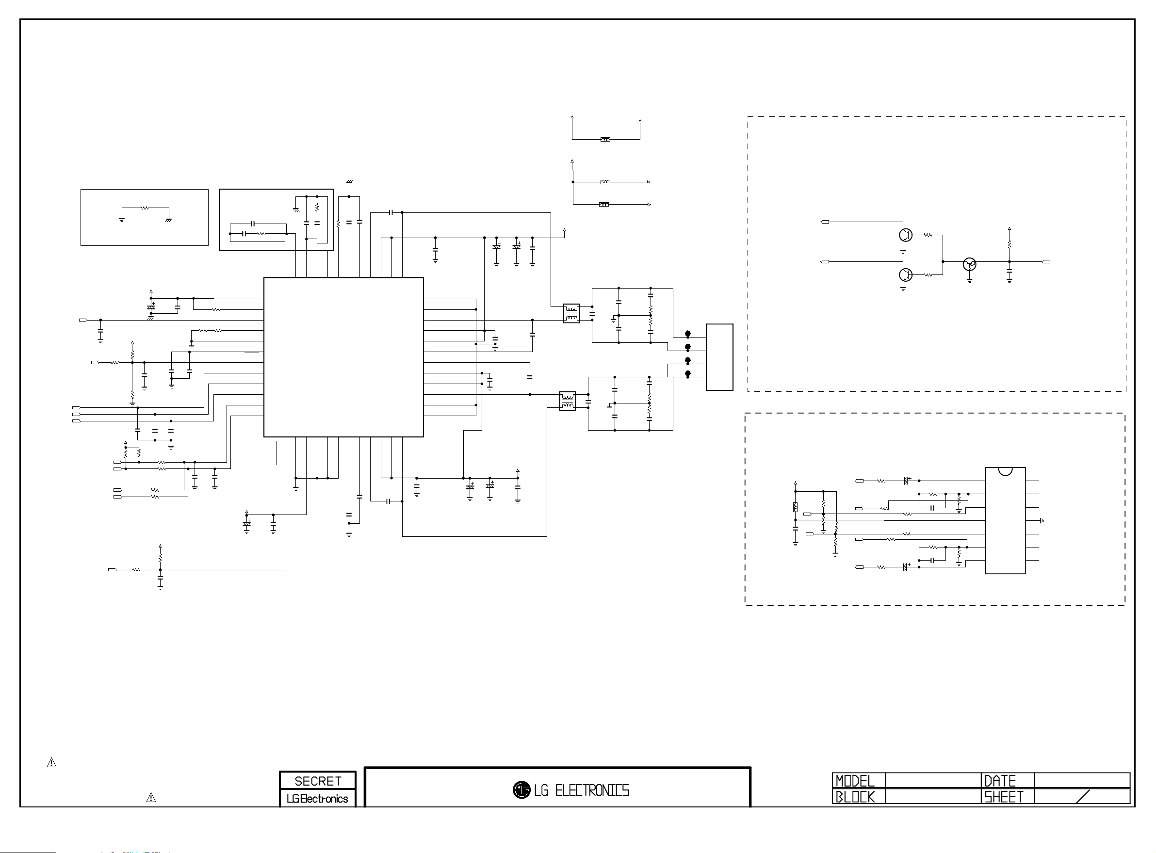
001:Z13
Copyright © 2010 LG Electronics Inc. All rights reserved.
Only for training and service purposes
LGE Internal Use Only
AUD_MASTER_CLK
011:I17;001:V10
AUD_LRCK
AUD_SCK
AUD_LRCH
004:E17;001:Y15
004:M17;001:Y14
004:E17;001:Y15
004:M17;001:Y14
AMP
Separate DGND AND AVSS
R742
22pF
READY
SDA2_3.3V
SCL2_3.3V
SDA3_3.3V
SCL3_3.3V
001:O19
AMP_RESET_N
READY
R70 0
0
PULL DOWN
+3.3V_DVDD
AC_DET
+3.3V_DVDD
R703
22K
READY
R728
2.2K
R704
33
R705
0
+3.3V_AU_AVDD
AVSS
R702
1K
C700
1000pF
50V
READY
C747
22pF
READY
READY
R744
2.2K
R707 33
R708 33
READY
R701 33
R736 33
READY
+3.3V_DVDD
C702
1000pF
READY
C701
10uF 16V
C748
22pF
READY
READY
R706
2K
AVSS
C703
0.1uF
C750
22pF
READY
C704
0.01uF
C705
4.7uF
16V
READY
This parts are Located
on AVSS area.
C710
C708
0.047uF
AVDD
TESTOUT
R710 0
READY
1/16W
MCLK
5%
R709
1%
OSC_RES
200
1%
18K
DVSS_1
R711
VR_DIG
LRCLK
SCLK
SDIN
C707
C706
33pF
33pF
READY
+3.3V_DVDD
PDN
SDA
SCL
C709
10uF 16V
4700pF
R712
470
13
14
15
16
17
18
19
20
21
22
23
24
C711
0.01uF
AVSS
PLL_FLTP
VR_ANA
11
12
25RESET
26STEST
R713
470
4700pF
C713
0.047uF
C712
AVSS
PLL_FLTM
8NC9
10
TAS5709PHPR
IC700
27DVDD
28DVSS_2
29GND
AVSS
22K
R714
SSTIMER
OC_ADJ
6
7
30AGND
31VREG
C715
0.1uF
C719
1uF
0.033uF
50V
C71 6
C714 2200pF
PVDD_A_1
PVDD_A_2
BST_A
GVDD_OUT_1
3
4
5
32GVDD_OUT_2
33BST_D
34PVDD_D_1
1uF
C71 7
C718
0.01uF
OUT_A
1
2
48
47
46
45
44
43
42
41
40
39
38
37
35PVDD_D_2
36OUT_D
0.033uF
50V
C721
PGND_AB_2
PGND_AB_1
OUT_B
PVDD_B_2
PVDD_B_1
BST_B
BST_C
PVDD_C_2
PVDD_C_1
OUT_C
PGND_CD_2
PGND_CD_1
C720
0.01uF
C722
47uF
25V
C726
0.01uF
C725
0.01uF
C723
47uF
25V
C724
47uF
25V
C727
47uF
25V
+17V_AMP
C728
10uF
25V
C729
10uF
25V
50V
0.033uF
C731
50V
0.033uF
C730
P_17V
0LCML00003B
MLB-201209-0120P-N2
+3.3V_MULTI
120-ohm
120-ohm
+17V_AMP
L701
AD-9060
2S
2F
C733
1S 1F
EAP61008401
L700
AD-9060
2S
1S 1F
EAP61008401
0.68uF
2F
C732
0.68uF
L704
L703
L702
C734
0.1uF
C735
0.1uF
C736
0.1uF
C737
0.1uF
+17V_AMP
+3.3V_AU_AVDD
+3.3V_DVDD
C740
0.01uF
R717
3.3
R718
3.3
C741
0.01uF
C738
0.01uF
R715
3.3
R716
3.3
C739
0.01uF
SPK_L+
SPK_L-
SPK_R+
SPK_R-
WAFER-ANGLE
4
3
2
1
P703
TV_L/ROUT
MNT/DTV OUT
MUTE Ctrl
TV_LOUT
TV_ROUT
P_17V
L705
C742
0.1uF
25V
120-ohm
SCART1_Lout_P
SCART1_Rout_P
Q705
2SC3052
Q702
2SC3052
Audio Out Amp
R719
2K
TV_LOUT
SCART1_Rout_N
R720
2K
TV_ROUT
R730
5.6K
R731
5.6K
READY
R732
READY
R733
47K
47K
READY
READY
R734
R735
47K
47K
SCART1_Lout_N
R729 2K
C744
10uF
35V
R721
5.6K
R722
5.6K
C743
10uF
35V
R727
2K
1/16W
5%
5%
1/16W
R723 33K
C745 33pF
R724 33K
C746 33pF
Q701
RT1P141C-T112
3
2
R725
10K
R726
10K
+3.3V_ST
READY
R1070
10K
1
1
2
3
4
5
6
7
C749
0.1uF
IC701
LM324D
1
2
3
4
5
6
7
14
13
12
11
10
9
8
SCART1_MUTE
14
13
12
11
10
9
8
THE SYMBOL MARK OF THIS SCHEMETIC DIAGRAM INCORPORATES
SPECIAL FEATURES IMPORTANT FOR PROTECTION FROM X-RADIATION.
FILRE AND ELECTRICAL SHOCK HAZARDS, WHEN SERVICING IF IS
ESSENTIAL THAT ONLY MANUFATURES SPECFIED PARTS BE USED FOR
THE CRITICAL COMPONENTS IN THE SYMBOL MARK OF THE SCHEMETIC.
BCM3556-C0
AUDIO AMP
10/01/
7 13
Page 19
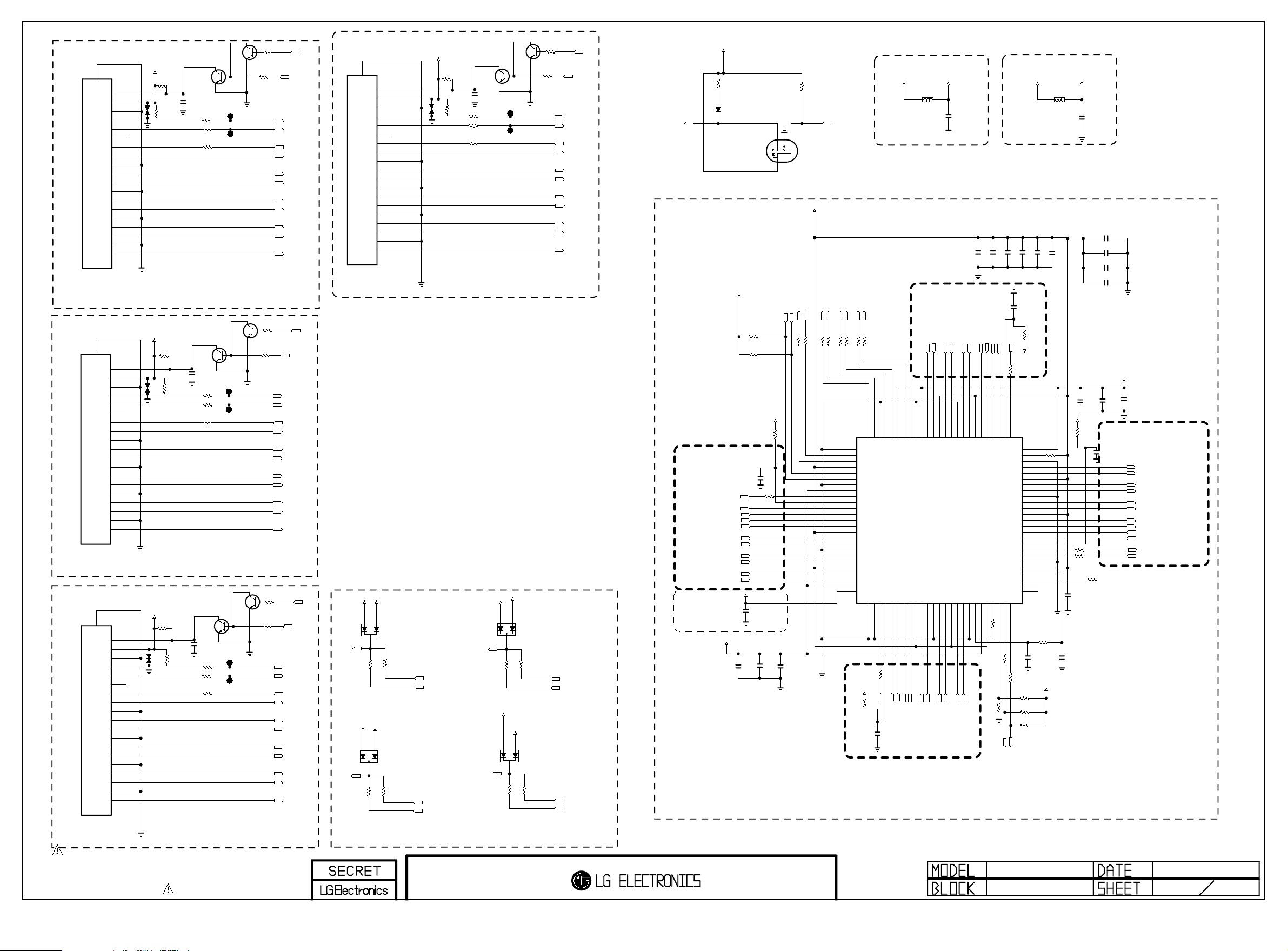
SHIELD
Copyright © 2010 LG Electronics Inc. All rights reserved.
Only for training and service purposes
LGE Internal Use Only
EAG59023302
JK800
SHIELD
$0.47
->$0.27
EAG59023302
JK801
SHIELD
$0.47
->$0.28
20
19
18
17
16
15
14
13
12
11
10
9
8
7
6
5
4
3
2
1
20
19
18
17
16
15
14
13
12
11
10
9
8
7
6
5
4
3
2
1
20
19
18
17
16
15
14
13
12
11
10
9
8
EAG59023301
7
6
5
4
3
2
1
CK+
D0-
D0_GND
D0+
D1-
D1_GND
D1+
D2-
D2_GND
D2+
CK+
D0-
D0_GND
D0+
D1-
D1_GND
D1+
D2-
D2_GND
D2+
CK+
D0-
D0_GND
D0+
D1-
D1_GND
D1+
D2-
D2_GND
D2+
GND
GND
5V_HDMI_1
R801
1K
2K
D806
READY
AVRL161A1R1NT
5V_HDMI_2
R805
D809
AVRL161A1R1NT
5V_HDMI_3
R804
1K
D807
READY
AVRL161A1R1NT
1K
R802
R800
R803
3.6K
3.6K
READY
READY
KRC104S
C800
0.1uF
16V
Q800
R809 22
R810
R811
Q801
KRC104S
C801
0.1uF
16V
R814 22
R815
R812
Q802
KRC104S
C802
0.1uF
16V
R816
R813 22
R817
C
E
+5V_MULTI
47K
+5V_MULTI
R831
47K
Q807
KRC104S
B
A1CA2
ENKMC2838-T112
D802
A1CA2
C
R834
B
E
R829
R832
47K
ENKMC2838-T112
D803
R833
47K
10K
10K
5V_HDMI/MULTI_4
DDC_SDA_4
DDC_SCL_4
CEC_REMOTE
CK-_HDMI4
CK+_HDMI4
D0-_HDMI4
D0+_HDMI4
D1-_HDMI4
D1+_HDMI4
D2-_HDMI4
D2+_HDMI4
DDC_SDA_1
DDC_SCL_1
DDC_SDA_4
DDC_SCL_4
HPD4
+3.3V_ST
R835
27K
D805
MMBD301LT1G
30V
S
BSS83
Q808
G
HDMI S/W For Platform
+5V_MULTI
R839
1.8K
R838
1.8K
5V_HDMI_1
C807
0.1uF
C804
0.1uF
16V
16V
C805
0.1uF
READY
R846
C806
0.1uF
16V
0
0
008:I19
008:H26;008:O8
008:H26;008:O8
HDMI1
HPD1
DDC_SDA_1
DDC_SCL_1
CK-_HDMI1
CK+_HDMI1
D0-_HDMI1
D0+_HDMI1
D1-_HDMI1
D1+_HDMI1
D2-_HDMI1
D2+_HDMI1
+5V_MULTI
+1.8V_HDMI
B D
008:AA19
HDMI_SDA
READY
R843
C808
0.1uF
16V
R837
100K
+3.3V_HDMI
008:AA19
003:D4
003:D4
HDMI0_RXC-_BCM
HDMI0_RXC+_BCM
HDMI_SCL
R867 0
R868 0
HDMI_CECCEC_REMOTE
003:D4
003:D4
003:D4
HDMI0_RX0+_BCM
HDMI0_RX1-_BCM
HDMI0_RX1+_BCM
VSS_1
OUT_C+
OUT_C-
VDDO[3V3]
VSS_2
RXA_HPD
RXA_5V
RXA_CRXA_C+
RXA_D0RXA_D0+
VSS_3
RXA_D1RXA_D1+
RXA_D2RXA_D2+
AUX_5V
5V_HDMI_3
HPD3
003:D4
HDMI0_RX2-_BCM
0
1
2
3
4
5
6
7
8
9
10
11
12
13
14
15
16
17
18
19
20
21
22
23
24
25
0
C809
0.1uF
003:D4
HDMI0_RX0-_BCM
R8690R8700R8710R8720R8730R874
OUT_DDC_CLK
OUT_DDC_DAT
VDDDC[1V8]_1
RXA_DDC_DAT
RXA_DDC_CLK
VDDH[3V3]_1
VDDH[3V3]_2
VDDH[1V8]_1
D1.8V
BLM18PG121SN1D
+1.8V_HDMI
L800
C810
0.1uF
16V
D3.3V
+3.3V_HDMI
BLM18PG121SN1D
L801
C822
0.1uF
16V
NEED TO CHECK THE CASE OF INSTANT BOOT
C824
0.1uF
C819
0.1uF
16V
0
READY
R866
0
C820
0.1uF
C821
0.1uF
16V
READY
R848
R862
0
R863 0
READY
C825
C826
C827
0.1uF
0.1uF
0.1uF
C823
0.1uF
16V
+1.8V_HDMI
C828
0.1uF
16V
003:D4
HDMI0_RX2+_BCM
OUT_D1+
OUT_D1-
VSS_1299OUT_D0+
OUT_D0-
96
97
98
100
26
28
29
30
VSS_427TEST1
RXB_5V
RXB_HPD
RXB_DDC_DAT
0
R864
READY
READY
R844
008:I19
16V
SIDE_HDMI
VDDDC[1V8]_3
VSS_11
OUT_D2+
OUT_D2-
VDDO[1V8]
92
93
94
95
IC800
TDA19997
31
32
34
RXB_C-33RXB_C+
RXB_D0-36RXB_D0+
RXB_DDC_CLK
VDDH[3V3]_3
CK-_HDMI3
CK+_HDMI3
DDC_SDA_3
DDC_SCL_3
HDMI3
D2+_HDMI4
RXD_D2-
RXD_D2+
90
91
35
VSS_5
D0-_HDMI3
D0+_HDMI3
D2-_HDMI4
D1+_HDMI4
RXD_D1+
VDDH[3V3]_8
87
88
89
37
38
RXB_D1-39RXB_D1+
D1-_HDMI3
D1+_HDMI3
D0+_HDMI4
D1-_HDMI4
RXD_D0-
RXD_D0+
VSS_1086RXD_D1-
83
84
85
40
41
43
VSS_6
RXB_D2-42RXB_D2+
VDDH[3V3]_4
D2+_HDMI3
D2-_HDMI3
C811
0.1uF
C812
D0-_HDMI4
CK+_HDMI4
RXD_C-
RXD_C+
VDDH[3V3]_7
80
81
82
44
45
46
CDEC_DDC
VDDDC[1V8]_2
VDDDC[1V8]_4
R854
0.1uF
CK-_HDMI4
DDC_SCL_4
RXD_DDC_CLK
79
47
TEST2
R853 0
C815
0.1uF
C813
0.1uF
0.1uF
C814
008:T28
0
DDC_SDA_4
HPD4
5V_HDMI_4
0
READY
R865
RXD_HPD
RXD_5V78RXD_DDC_DAT
76
77
VDDH[1V8]_2
75
R12K
74
VSS_9
73
RXC_D2+
72
RXC_D2-
71
VDDH[3V3]_6
70
RXC_D1+
69
RXC_D1-
68
VSS_8
67
RXC_D0+
66
RXC_D0-
65
VDDH[3V3]_5
64
RXC_C+
63
RXC_C-
62
RXC_DDC_CLK
61
RXC_DDC_DAT
60
RXC_5V
59
RXC_HPD
58
CEC
57
VSS_7
56
VDDS[3V3]
55
CDEC_STBY
54
INT_N/MUTE
53
RXE_DDC_DAT
52
RXE_DDC_CLK
51
48PD49
I2C_SDA50I2C_SCL
R855 1
R856 1
R857
10
READY4.7K
1.2K
R858
1.2K
R859
SCL2_3.3V
SDA2_3.3V
001:I4;007:E14;007:K5;025:AE10;027:U11
001:I4;007:C12;007:K5;025:AF10;027:U10
C817
0.1uF
READY
R847
0
R860
READY
C816
0.1uF
16V
+3.3V_HDMI
0.1uF
5V_HDMI_2
R861
12K
C818
C829
0.1uF
16V
D2+_HDMI2
D2-_HDMI2
D1+_HDMI2
D1-_HDMI2
D0+_HDMI2
D0-_HDMI2
CK+_HDMI2
CK-_HDMI2
DDC_SCL_2
008:H8;008:T4
008:H8;008:T4
DDC_SDA_2
HPD2
008:H10
CEC_REMOTE
005:E5;008:H17;008:H26;008:H7;008:S25;008:Z26;008:AE26
HDMI2
C
10K
R808
Q803
KRC104S
C
E
22
0
KRC104S
C
E
22
0
B
E
10K
R806
B
C
R818
Q804
B
E
10K
R807
B
10K
CEC_REMOTE
CK-_HDMI2
CK+_HDMI2
D0-_HDMI2
D0+_HDMI2
D1-_HDMI2
D1+_HDMI2
D2-_HDMI2
D2+_HDMI2
HPD1
5V_HDMI/MULTI_1
DDC_SDA_1
DDC_SCL_1
CEC_REMOTE
CK-_HDMI1
CK+_HDMI1
D0-_HDMI1
D0+_HDMI1
D1-_HDMI1
D1+_HDMI1
D2-_HDMI1
D2+_HDMI1
HPD2
5V_HDMI/MULTI_2
DDC_SDA_2
DDC_SCL_2
JACK_GND
JK803
20
19
18
17
16
15
14
13
12
11
10
9
8
EAG42463001
7
6
5
4
3
2
1
CK+
D0-
D0_GND
D0+
D1-
D1_GND
D1+
D2-
D2_GND
D2+
SIDE HDMI
5V_HDMI_4
R826
1K
READY
3.6K
D808
R825
READY
AVRL161A1R1NT
GND
KRC104S
R827 22
R828 22
R836 0
C803
0.1uF
16V
Q806
EDID Pull-up
C
10K
R820
Q805
KRC104S
C
E
22
0
B
E
10K
R819
B
HPD3
5V_HDMI/MULTI_3
DDC_SDA_3
DDC_SCL_3
CEC_REMOTE
CK-_HDMI3
CK+_HDMI3
D0-_HDMI3
D0+_HDMI3
D1-_HDMI3
D1+_HDMI3
D2-_HDMI3
D2+_HDMI3
5V_HDMI/MULTI_2
5V_HDMI/MULTI_3
R822
47K
5V_HDMI_3
R821
47K
+5V_MULTI5V_HDMI_2
A1CA2
+5V_MULTI
A1CA2
ENKMC2838-T112
D800
ENKMC2838-T112
D801
R824
47K
R823
47K
DDC_SDA_2
DDC_SCL_2
DDC_SDA_3
DDC_SCL_3
5V_HDMI_1
5V_HDMI/MULTI_1
R830
5V_HDMI_4
5V_HDMI/MULTI_4
JK802
GND
THE SYMBOL MARK OF THIS SCHEMETIC DIAGRAM INCORPORATES
SPECIAL FEATURES IMPORTANT FOR PROTECTION FROM X-RADIATION.
FILRE AND ELECTRICAL SHOCK HAZARDS, WHEN SERVICING IF IS
ESSENTIAL THAT ONLY MANUFATURES SPECFIED PARTS BE USED FOR
THE CRITICAL COMPONENTS IN THE SYMBOL MARK OF THE SCHEMETIC.
HDMI MUX/HDMI
BCM3556-C0
HDMI
10/01
6 13
Page 20
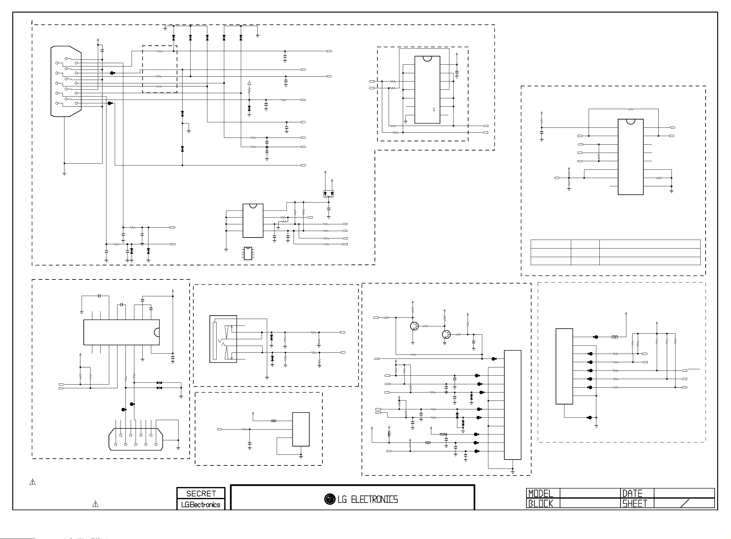
RGB
Copyright © 2010 LG Electronics Inc. All rights reserved.
Only for training and service purposes
LGE Internal Use Only
1
2
3
4
5
P900
SPG09-DB-010
6
11
7
12
8
13
9
14
10
15
16
SHILED
GND
RED_GND
GND_2
RED
GREEN_GND
DDC_DATA
GREEN
BLUE_GND
H_SYNC
BLUE
NC
V_SYNC
GND_1
SYNC_GND
DDC_CLOCK
DDC_GND
+5V_VGA
C900
0.1uF
16V
C901
270pF
50V
READY
R902
10
C906
220pF
50V
READY
C905
220pF
50V
READY
READY
R903
10
READY FOR BEAD
bcm REF circuit
R943 0
R942
R944 0
C908
220pF
50V
READY
D901
D900
READY
D904
0
D918 D917
ROM DOWNLOAD FOR PDP
PC_SER_DATA
PC_SER_CLK
D905
D907
D906
+3.3V_MULTI
M24C02 COMPARE THE COST
AT24C02BN-10SU-1.8
STM_2K_EEPROM
R1EX24002ASAS0A
A0
A1
A2
VSS
RENESAS_2K_EEPROM
D908
R911
30V
D909
1
2
3
4
IC901-*1
1
2
3
4
10K
R915
10
R916
10
IC901
VCC
8
WP
7
SCL
6
SDA
5
READY
8
7
6
5
READY
C914
0.1uF
16V
C918
18pF
50V
R917
1K
C916
12pF
12pF
C917
R922 100
R913
C919
18pF
50V
READY
C912
4.7pF
READY
C913
4.7pF
READY
C915
4.7pF
10K
DDC_SDA/UART_TX
DSUB_DET
DSUB_B
DSUB_HSYNC
DSUB_VSYNC
DDC_SCL/UART_RX
R924
R923
2.7K
2.7K
+5V_VGA
EDID_WP
+5V_MULTI
A1CA2
R929
1
R930
1
R932
22
R934
22
DSUB_R
DSUB_G
ENKMC2838-T112
D912
C922
0.1uF
RGB_HSYNC
003:B2
RGB_VSYNC
003:B2
DDC_SCL/UART_RX
DDC_SDA/UART_TX
DDC_SCL
DDC_SDA
RGB V/HSYNC BUUFFER
IC903
74F08D
D0A
1
14
D0B
2
R953
22
R959
22
READY
R960
22
READY
R961
22
BCM Reference
Q0
D1A
D1B
Q1
GND
13
3
12
4
11
5
10
6
7
9
8
+5V_MULTI
VCC
D3B
D3A
Q3
D2B
D2A
Q2
C928
0.1uF
DSUB_VSYNC
DSUB_HSYNC
M/R UART SWITCH
+3.3V_MULTI
R91 8
0
M_REMOTE
C904
0.1uF
M_REMOTE_MOD_ROM_TX
M_REMOTE_MOD_ROM_RX
REMOTE_SW_CTRL
M_REMOTE_RX
MOD_ROM_RX
+3.3V_MULTI
4.7K
R908
47K
R909
READY
NON_M_REMOTE
READY
R95 1
0
M_REMOTE & MOD_ROM_DL
SELECT PIN
X1/Y1/Z1HIGH
LOW
MODULE ROM DL CONNECT --> BCM UARTX0/Y0/Z0
NON_M_REMOTE
0
R95 5
IC902
MC14053BDR2G
VDD
16
Y
15
X
14
X1
13
X0
12
A
11
B
10
C
9
Y1
1
Y0
2
Z1
3
Z
4
Z0
5
INH
6
VEE
0
7
M_REMOTE
VSS
8
M_REMOTE
STATUSWIRELESS_SW_CTRL
M_REMOTE CONNECT --> BCM UART
M_REMOTE_TX
MOD_ROM_TX
R96 2
RS232C
RS232C_TXD
RS232C_RXD
+3.3V_ST
R900
4.7K
R901
4.7K
9
C902
0.1uF
50V
ROU T2
DOU T28RIN 2
7
10
DIN 2
P901
SPG09-DB-009
C907
0.1uF
50V
6V-5
IC900
MAX3232CDR
11
12
DIN 1
R904
100
1
+3.3V_ST
C909
0.1uF
50V
C910
0.1uF
50V
C1-2V+
C2+
C2-
3
4
13
14
RIN 1
ROU T1
R905
100
6
7
2
C1+
1
15
GND16VCC
DOU T1
D902
30V
8
9
3
4
5
D903
C911
0.1uF
50V
30V
10
PC AUDIO
JK900
PEJ027-01
E_SPRING
3
T_TERMINAL1
6A
B_TERMINAL1
7A
R_SPRING
4
T_SPRING
5
B_TERMINAL2
7B
T_TERMINAL2
6B
FOR PK/J90 - BREATING
+5V_MULTI
LED_PK90
R988
LED_BREATHING
10
C929
10pF
READY
D910
5.6V
D911
5.6V
LED_PK90
L903
MLB-201209-0120P-N2
READY
R926
470K
READY
R927
470K
LED_PK90
12507WR-03L
1
2
3
P907
R931
0
READY
R935
12K
R933
0
READY
R936
12K
4
PC_R_IN
PC_L_IN
SUB Board I/F
+3.3V_ST
R914
+3.3V_ST
R941
R938
10K
+3.3V_MULTI
R906
4.7K
READY
4.7K
READY
47K
Q901
2SC3052
10K
R907
+3.3V_MULTI
IR_NEC
SUB_SCL
SUB_SDA
+5V_MULTI
IR
LED_WHITE
R910
22
KEY1
KEY2
LED_RED
+3.3V_MULTI
L902
READY
C
B
E
READY
R912
0
R937
10K
C923
10pF
READY
MLB-201209-0120P-N2
R939
4.7K
R921
10K
READY
C924
10pF
+3.3V_ST
L901
R945
22
R946
22
R947
22
+3.3V_ST
R925
47K
C
B
Q902
E
2SC3052
C926
10pF
L900
MLB-201209-0120P-N2
C927
0.1uF
16V
READY
R940
10K
R928
47K
C903
C930
10pF
C931
10pF
D915
CDS3C05HDMI1
5.6V
D916
CDS3C05HDMI1
5.6V
C932
0.1uF
16V
10pF
C933
10pF
+3.3V_ST
D913
KEY1
KEY2
LED-RED
3.3V_ST
3.3V_MULTI
LED-WHITE
IR
GND
GND
SCL
SDA
GND
P906
12507WS-12L
1
2
3
4
5
6
7
8
9
10
11
12
13
GND
MOTION REMOTE
P902
12507WR-08L
9
M_REMOTE
+3.3V_MULTI
+3.3V_MULTI
L904
1
2
3
4
5
6
7
8
120-ohm
BLM18PG121SN1D
R919
100
R920
100
R948
100
R949
100
R950
100
R952
4.7K
READY
READY
R954
4.7K
R956
2.7K
M_REMOTE_RX
M_REMOTE_TX
R957
2.7K
R958
2.7K
RF_RESET
DC
DD
THE SYMBOL MARK OF THIS SCHEMETIC DIAGRAM INCORPORATES
SPECIAL FEATURES IMPORTANT FOR PROTECTION FROM X-RADIATION.
FILRE AND ELECTRICAL SHOCK HAZARDS, WHEN SERVICING IF IS
ESSENTIAL THAT ONLY MANUFATURES SPECFIED PARTS BE USED FOR
THE CRITICAL COMPONENTS IN THE SYMBOL MARK OF THE SCHEMETIC.
BCM3556-C0
LVDS/RS232//RGB
10/01/
10 13
Page 21
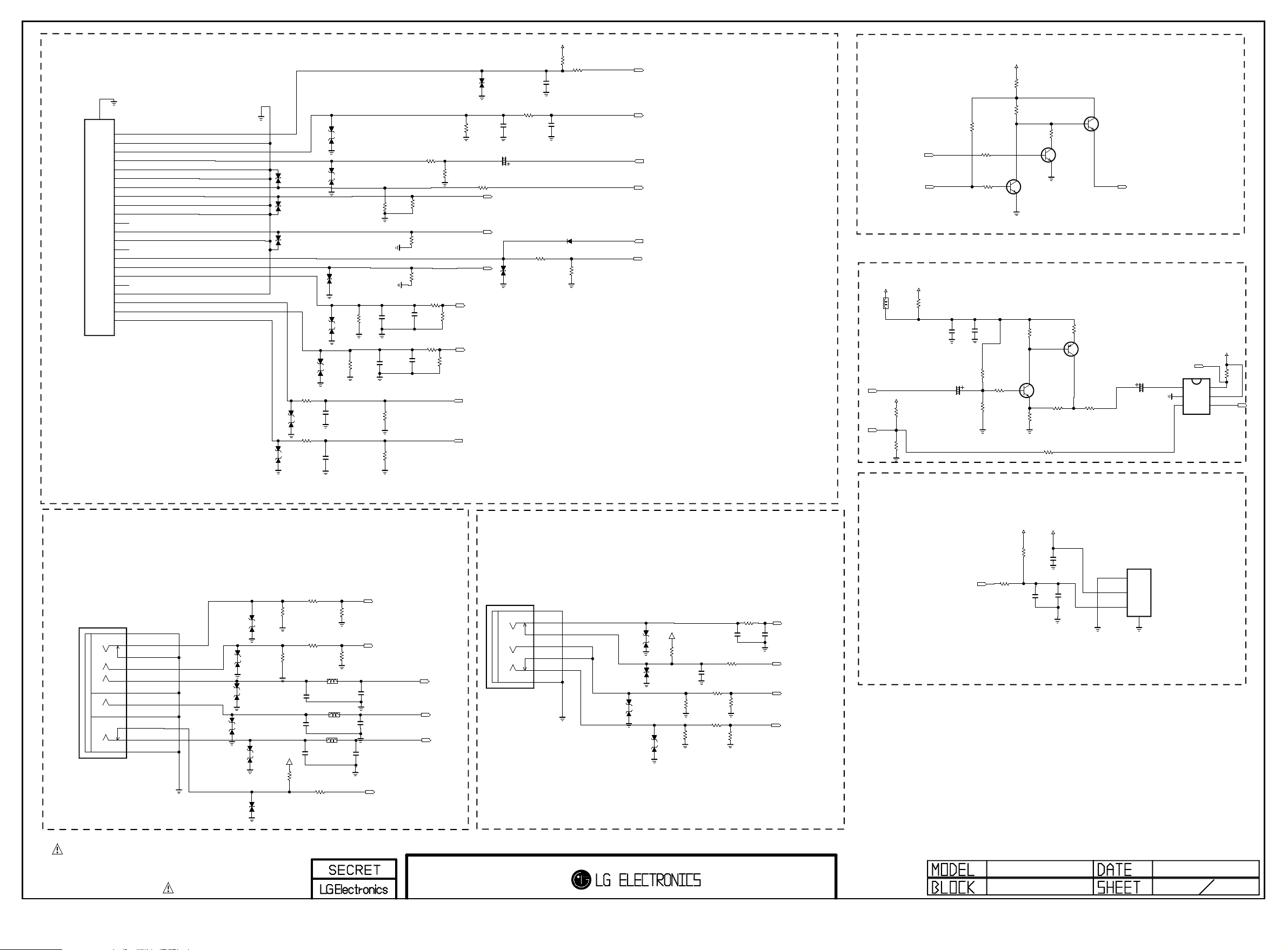
Full SCART 1
Copyright © 2010 LG Electronics Inc. All rights reserved.
Only for training and service purposes
LGE Internal Use Only
SHIELD
23
22
AV_DET
21
COM_GND
20
SYNC_IN
19
SYNC_OUT
18
SYNC_GND2
17
SYNC_GND1
16
RGB_IO
15
R_OUT
14
RGB_GND
13
R_GND
12
D2B_OUT
11
G_OUT
.
10
.
9
8
SC_ID
B
7
6
LIN
5
GND
4
GND
3
L_OUT
2
R_IN
1
R_OUT
PSC008-02
JK1001
D1012
D1013
D1008
30V
D1009
30V
D1010
30V
D1014
D1019
5.1V
5.1V
5.1V
5.1V
R1002
1K
R1003
1K
D1020
D1021
D1023
D1024
D1025
D1026
D1027
D1028
5.1V
5.1V
5.1V
5.1V
5.1V
5.1V
D1015
30V
5.1V
C1002
6800pF
50V
C1003
6800pF
50V
5.1V
R1008
470K
R1011
470K
R1022
75
READY
C1006
OPT
READY
C1005
OPT
R1020
470K
READY
R1021
470K
READY
READY
R1009
75
READY
READY
R1018
75
R1010
75
C1007
330pF
50V
READY
C1008
330pF
50V
READY
R1023
75
R1024
0
R1025
0
R1027
12K
READY
R1028
12K
READY
R1029
470K
R1013
75
SC1_L_IN
SC1_R_IN
TV_LOUT
TV_ROUT
READY
D1016
30V
READY
R1030
22
SC1_R
SC1_G
SC1_B
C1010
100uF
16V
C1000
220pF
50V
READY
D1017
30V
READY
+3.3V_MULTI
R1031
0
R1032
15K
C1012
0.1uF
16V
C1011
220pF
50V
READY
R1033
10K
30V
D1018
R1035
1K
R1034
3.9K
SCART1_DET
SC1_CVBS_IN
SC1_VOUT
SC1_FB
REC_8
SC1_ID
[SCART1 PIN 8]
SC_RE1
SC_RE2
[SCART TV VOUT]
+5V_MULTI
P_17V
R1041
0
READY
BLM18PG121SN1D
L1000
ATV_OUT
+5V_MULTI
R1026
27K
READY
DTV/MNT_V_OUT
R1044
27K
READY
C1021
47uF
16V
C1019
0.1uF
25V
R1056
R1057
27K
15K
R1050
7.5K
C1018
0.1uF
25V
R1053
1K
R1054
1K
P_17V
R1059
3K
R1060
10K
R1063
12K
C
Q1004
B
2SC3052
E
C
Q1002
B
2SC3052
E
120
R1061
B
C
Q1003
B
R1014
82
R1062
2SC3052
E
R1065
330
150
R1012
0
R1069
C
Q1006
B
2SC3052
E
REC_8
22
E
ISA1530AC1
Q1005
C
R1046
0
C1033
25V
100uF
DTV_ATV_SELECT
GND
B0
IC1001
NLASB3157DFT2G
1B16
2
3
SELECT
VCC
5
A
4
+5V_MULTI
10K
R1045
SC1_VOUT
COMPONENT
JK1000
PPJ234-01
[RD]E-LUG
6E
[RD]O-SPRING_2
5E
[RD]CONTACT
4E
[WH]O-SPRING
5D
[RD]O-SPRING_1
5C
[RD]E-LUG-S
7C
[BL]O-SPRING
5B
[BL]E-LUG-S
7B
[GN]CONTACT
4A
[GN]O-SPRING
5A
[GN]E-LUG
6A
GND
D1001
D1002
D1005
D1006
D1003
D1004
5.1V
5.1V
D1035
D1036
5.1V
5.1V
5.1V
5.1V
D1007
D1011
D1000
30V
5.1V
5.1V
5.1V
5.1V
470K
R1000
470K
R1001
+3.3V_MULTI
R1004
10K
R1005
0
R1006
0
CM2012FR27KT
C1020
27pF
CM2012FR27KT
C1017
27pF
CM2012FR27KT
C1004
27pF
R1007
1K
READY
READY
L1002
L1003
L1001
R1015
12K
12K
R1016
C1031
27pF
C1027
27pF
C1026
27pF
COMP_R_IN
COMP_L_IN
COMP_DET
COMP_Pr
COMP_Pb
COMP_Y
SIDE CVBS
5A
[YL]E-LUG
4A
[YL]O-SPRING
3A
[YL]CONTACT
4B
[WH]O-SPRING
3C
[RD]CONTACT
4C
[RD]O-SPRING
5C
PPJ235-01
[RD]E-LUG
JK1002
D1029
D1030
D1032
D1022
30V
5.1V
5.1V
D1031
D1033
D1034
5.1V
5.1V
+3.3V_MULTI
R1036
10K
5.1V
5.1V
SPDIF
+5V_MULTI
+5V_MULTI
R1058
1K
C1023
0.1uF
C1022
22pF
50V
C1024
10uF
16V
READY
R1051
SPDIF_OUT
R1017
0
READY
C1032
220pF
50V
R1019
1K
C1013
0.1uF
16V
R1040
0
12K
R1043
R1039
0
R1042
READY
READY
12K
470 K
R10 38
470 K
R10 37
C1016
220pF
50V
AV_CVBS_IN
SIDEAV_DET
SIDE_LIN
SIDE_RIN
100
VINPUT
JK1003
JST1223-001
GND
VCC
1
2
3
Fib er Op tic
4
FIX_POLE
THE SYMBOL MARK OF THIS SCHEMETIC DIAGRAM INCORPORATES
SPECIAL FEATURES IMPORTANT FOR PROTECTION FROM X-RADIATION.
FILRE AND ELECTRICAL SHOCK HAZARDS, WHEN SERVICING IF IS
ESSENTIAL THAT ONLY MANUFATURES SPECFIED PARTS BE USED FOR
THE CRITICAL COMPONENTS IN THE SYMBOL MARK OF THE SCHEMETIC.
BCM3556-C0
JACK
10/01/
9 13
Page 22
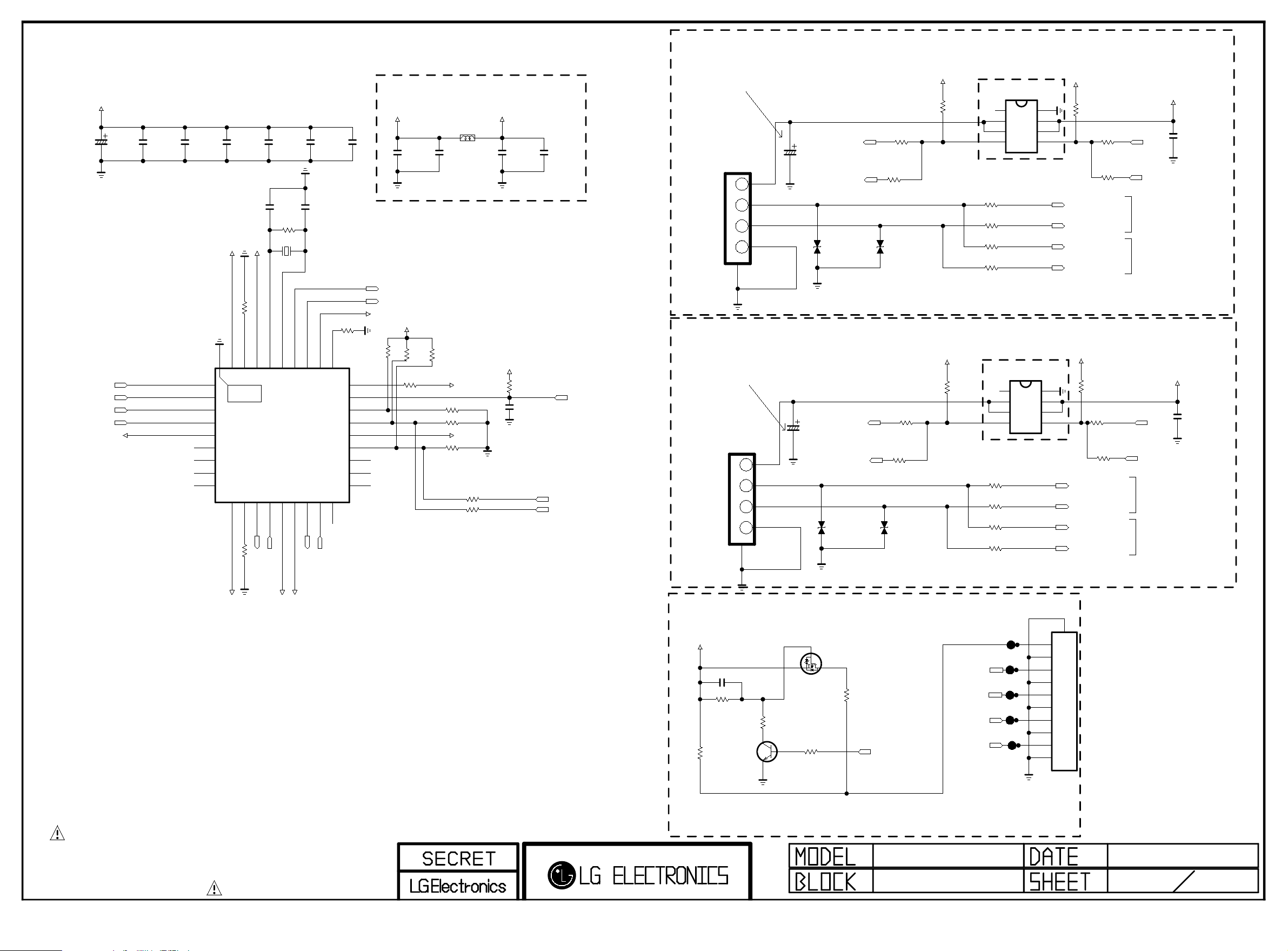
USB HUB
Copyright © 2010 LG Electronics Inc. All rights reserved.
Only for training and service purposes
LGE Internal Use Only
+3.3V_USB_HUB
C1100
16V
100uF
USB1_DM_to_HUB
USB1_DP_to_HUB
USB2_DM_to_HUB
USB2_DP_to_HUB
+3.3V_USB_HUB
C1101
0.1uF
16V
C1102
0.1uF
16V
USBDN1_DM
USBDN1_DP
USBDN2_DM
USBDN2_DP
VDDA33_1
NC_1
NC_2
NC_3
NC_4
C1103
0.1uF
16V
+3.3V_USB_HUB
+1.8V_USB_HUB_PLL
R1100 12K
VDD18PLL
RBIAS
VDD33PLL
VSS
34
35
36
1
THERMAL
2
37
3
4
10
11
TEST
VDDA33_2
USB2512A_AEZG
12
PRTPWR1
5
6
7
8
9
C1104
0.1uF
16V
C1105
15pF
50V
USBUP_DP
XTAL2
XTAL1/CLKIN
31
32
33
IC1100
13
14
15
VDD18
OCS1_N
VDD33CR16PRTPWR2
C1107
0.1uF
16V
C1106
15pF
50V
R1102
1M
X1100
24MHz
VDDA33_3
USBUP_DM
29
30
17
OCS2_N
C1109
0.1uF
16V
R1104
+3.3V_USB_HUB
100K
SUSP_IND/LOCAL_PWR/NON_REM0
28
VBUS_DET
27
RESET_N
26
HS_IND/CFG_SEL1
25
SCL/SMBCLK/CFG_SEL0
24
VDD33
23
SDA/SMBDATA/NON_REM1
22
NC_8
21
NC_7
20
NC_6
19
18
NC_5
Power from USB2512 (OUTPUT)
READY
+1.8V_USB_HUB
C1110
1uF
10V
L1101
0LCML00003B
MLB-201209-0120P-N2
C1111
0.1uF
16V
USB_DP
USB_DM
+3.3V_USB_HUB
READY
READY
R1106
R1109
10K
R1108
4.7K
R1110
10K
+3.3V_USB_HUB
10K
READY
R1111 100K
R1112 100K
+3.3V_USB_HUB
R1113 100K
READY
R1115
33
R111633
READY
+1.8V_USB_HUB_PLL
C1112
1uF
10V
C1114
0.1uF
16V
+3.3V_USB_HUB
R1118
100K
C1113
0.1uF
16V
/RST_HUB
SDA1_3.3V
SCL1_3.3V
004:E17;001:Y15
004:E17;001:Y15
004:M17;001:Y14
USB1 SIDE UPPER
Capacitors on VBUSA should be
placed as closd to connector as possible.
P1101
EAG41945401
KJA-UB-4-0004
1
USB DO WN STRE AM
C1116
100uF
16V
USB1_OCD
USB1_OCD_HUB
2
3
D1100
4
5
CDS3C05HDMI1
5.6V
+3.3V_USB_HUB
R1124 0
R1122 0
READY
D1102
CDS3C05HDMI1
5.6V
USB2 SIDE UNDER
Capacitors on VBUSA should be
placed as closd to connector as possible.
R1125 0
R1123 0
READY
D1103
CDS3C05HDMI1
5.6V
P1102
EAG41945401
KJA-UB-4-0004
1
USB DO WN STRE AM
2
3
4
5
C1117
100uF
16V
D1101
CDS3C05HDMI1
5.6V
USB2_OCD
R1129
10K
+3.3V_USB_HUB
R1130
10K
OUT_2
OUT_1
R1133 0
R1134 0
R1135 0
R1136 0
R1137 0
R1138 0
R1139 0
R1140 0
SWITCH ADDED
+3.3V_USB_HUB
R1141
10K
READY
R1145 0
AP2191SG-13
NC
8
7
6
FLG
5
IC1101
GND
1
IN_1
2
IN_2
3
EN
4
R1146 0
USE_USB_HUB
USE_USB_HUB
USE_NO_HUB
USE_NO_HUB
SWITCH ADDED
IC1102
AP2191SG-13
NC
8
OUT_2
7
OUT_1
6
FLG
5
USB1_DM_to_HUB
USB1_DP_to_HUB
USB1_DM_to_MAIN
USB1_DP_to_MAIN
GND
1
IN_1
2
IN_2
3
EN
R1143 0
4
+3.3V_USB_HUB
R1142
10K
READY
R1144 0
READY
USE_USB_HUB
USE_USB_HUB
USB_NO_HUB&USB_2PORT
USB_NO_HUB&USB_2PORT
USB2_DM_to_HUB
USB2_DP_to_HUB
USB2_DM_to_MAIN
USB2_DP_to_MAIN
READY
+5V_USB
C1120
USB1_CTL
0.1uF
16V
USB1_CTL_HUB
USB1 Dato to USB2512
USB1 Dato to MAIN(S7)
+5V_USB
C1121
USB2_CTL
0.1uF
16V
USB2_CTL_HUBUSB2_OCD_HUB
USB2 Dato to USB2512
USB2 Dato to MAIN(S7)
R1101 0
USB1_CTL_HUB
USB1_OCD_HUB
+3.3V_USB_HUB
USB2_CTL_HUB
USB2_OCD_HUB
+1.8V_USB_HUB
+3.3V_USB_HUB
THE SYMBOL MARK OF THIS SCHEMETIC DIAGRAM INCORPORATES
SPECIAL FEATURES IMPORTANT FOR PROTECTION FROM X-RADIATION.
FILRE AND ELECTRICAL SHOCK HAZARDS, WHEN SERVICING IF IS
ESSENTIAL THAT ONLY MANUFATURES SPECFIED PARTS BE USED FOR
THE CRITICAL COMPONENTS IN THE SYMBOL MARK OF THE SCHEMETIC.
BLUETOOTH
+3.3V_MULTI
1uF
C1108
BLUE_TOOTH
R1105
BLUE_TOOTH
2SC3052
READY
R1103
0
Q1101
BLUE_TOOTH
47K
C
E
BLUETOOTH
R1107
47K
B
G
S
Q1103
BLUE_TOOTH
RTR030P02
BLUE_TOOTH
R1114
4.7K
D
R1117
10
BT_ON/OFF
BCM3556
USB HUB
BT_DM
BT_DP
BT_RESET
VREG_CTR
11
10
9
8
7
6
5
4
3
2
1
12507WS-10L
P1100
BLUE_TOOTH
10/01
13 13
Page 23
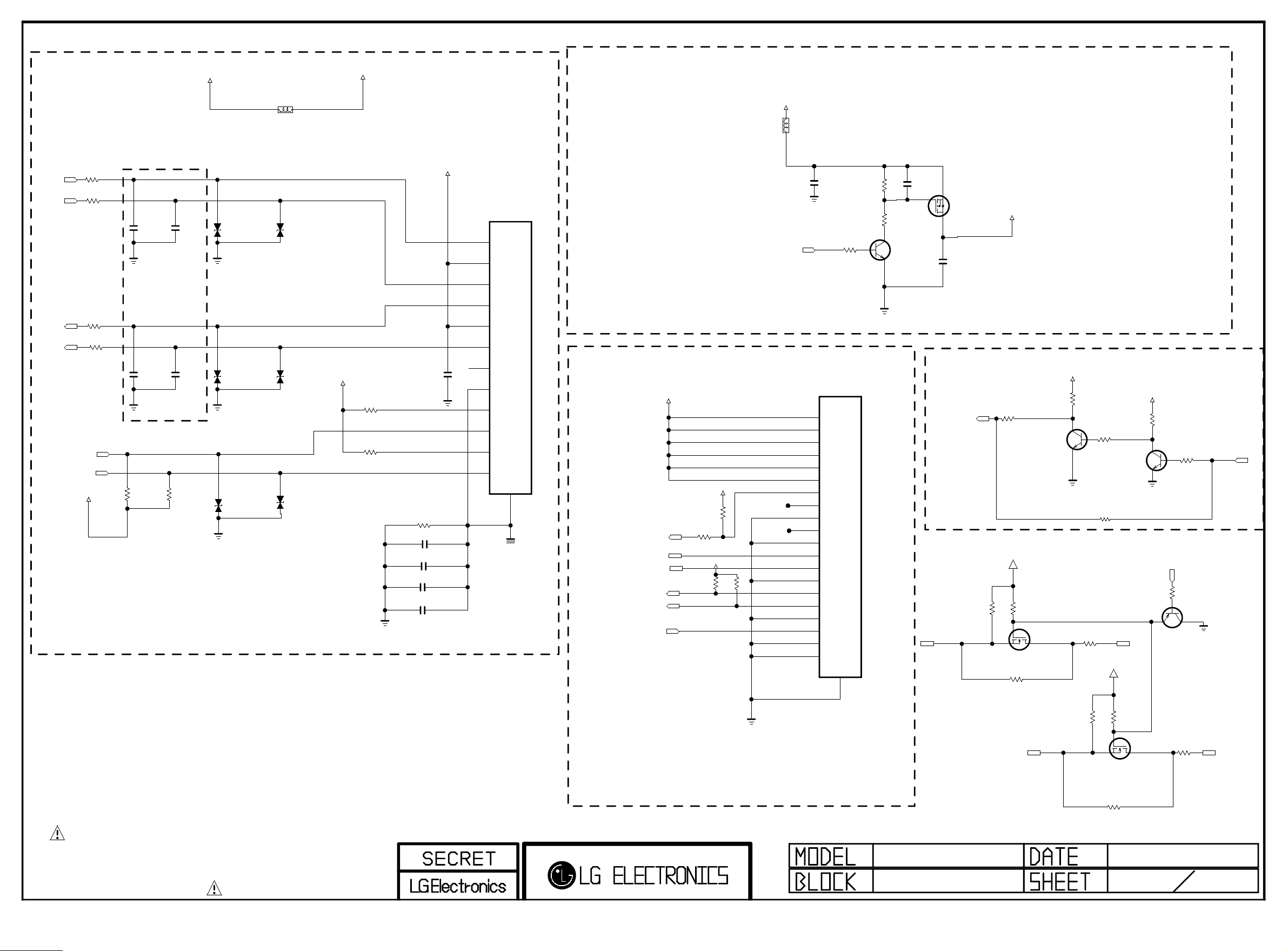
ETHERNET JACK
Copyright © 2010 LG Electronics Inc. All rights reserved.
Only for training and service purposes
LGE Internal Use Only
R1234
EPHY_TDP
EPHY_TDN
EPHY_RDP
EPHY_RDN
EPHY_ACTIVE_Y
0
EPHY_LINK
for EMI
R1235
0
READY
R1236
0
R1237
0
READY
R1200
+3.3V_MULTI
10K
C1200
10pF
50V
C1201
10pF
50V
READY
C1202
10pF
50V
READY
C1203
10pF
50V
R1201
10K
+3.3V_MULTI
D1202
5.5V
READY
EAH60667401
D1201
5.5V
READY
EAH60667401
D1200
5.5V
EAH60667401
WIRELESS MODEL
BLM18PG121SN1D
L1201
D1205
5.5V
READY
EAH60667401
D1204
5.5V
READY
EAH60667401
D1203
5.5V
EAH60667401
+3.3V_VA
+3.3V_VA
A2.5V
NEED PART : $0.85
JK1200
EAG35781001
XRJV-01V-D12-180
P1_TD+
1
P2_CT
2
P3_TD-
3
P4_RD+
4
P5_CT
5
P6_RD-
6
P7
C1208
0.022uF
50V
R1206
510
R1207
510
3216 TPYE : FOR ESD
R1208 0
C1207
READY
READY
READY
READY
0.1uF
16V
C1206
0.1uF
16V
C1204
0.01uF
50V
C1205
0.01uF
50V
FOR EMI
FOR EMI
FOR EMI
FOR EMI
7
P8
8
D1
D1
D2
D2
D3
D3
D4
D4
SHILED
ETERNET_GND
WIRELESS DIP POWER ON/OFF
P_17V
L1200
WIRELESS MODEL
BLM18PG121SN1D
WIRELESS MODEL
C1211
0.1uF
50V
WIRELESS MODEL
R1222
WIRELESS_PWR_EN
WIRELESS INTERFACE
P_17V_WIRELESS
VCC[24V/20V/17V]_1
VCC[24V/20V/17V]_2
VCC[24V/20V/17V]_3
VCC[24V/20V/17V]_4
VCC[24V/20V/17V]_5
VCC[24V/20V/17V]_6
9
WIRELESS MODEL
WIRELESS_DETECT
WIRELESS_SCL
WIRELESS_SDA
WIRELESS_DL_TX(WIRELESS_RX)
WIRELESS_DL_RX
WIRELESS_DL_RX(WIRELESS_TX)
WIRELESS_DL_TX
IR_PASS
R1210 1K
+3.3V_MULTI
R1214
10K
+3.3V_MULTI
R1215
R1213
4.7K
WIRELESS MODEL
WIRELESS MODEL
4.7K
WIRELESS MODEL
DETECT
INTERRUPT
GND_1
RESET
GND_2
I2C_SCL
I2C_SDA
GND_3
UART_RX
UART_TX
GND_4
GND_5
GND_6
10K
WIRELESS MODEL
JK1201
KJA-PH-3-0168
1
2
3
4
5
6
7
8
9
10
WIRELESS MODEL
11
12
13
14
15
16
17
IR
18
19
20
21
SHIELD
R1224
22K
R1225
2.2K
WIRELESS MODEL
C
B
WIRELESS MODEL
E
C1212
2.2uF
WIRELESS MODEL
G
Q1202
AO3407A
WIRELESS MODEL
WIRELESS MODEL
Q1201
WIRELESS IIC
S
D
C1213
0.01uF
50V
WIRELESS
IR_PASS
R1223
+3.3V_MULTI
R1203
10K
WIRELESS MODEL
WIRELESS MODEL
P_17V_WIRELESS
22
2SC3052
10K
R1205
G
WIRELESS MODEL
D
S
Q1200
2N7002(F)
R120422
READY
+3.3V_ST
R1226
47K
Q1203
WIRELESS MODEL
C
E
B
R1211
R1228
10K
READY
R1227
22
22
+3.3V_MULTI
R1230
Q1204
2SC3052
SDA2_3.3VWIRELESS_SDA
+3.3V_ST
47K
SIGN11824
C
E
R1231
47K
B
WIRELESS_PWR_EN
10K
R1233
B
WIRELESS MODEL
WIRELESS MODEL
E
C
Q1302
ISA1530AC1
IR
THE SYMBOL MARK OF THIS SCHEMETIC DIAGRAM INCORPORATES
SPECIAL FEATURES IMPORTANT FOR PROTECTION FROM X-RADIATION.
FILRE AND ELECTRICAL SHOCK HAZARDS, WHEN SERVICING IF IS
ESSENTIAL THAT ONLY MANUFATURES SPECFIED PARTS BE USED FOR
THE CRITICAL COMPONENTS IN THE SYMBOL MARK OF THE SCHEMETIC.
BCM3556-C0
ETHERNET
WIRELESS_SCL
R1216
10K
R1220
WIRELESS MODEL
G
WIRELESS MODEL
S
Q1205
2N7002(F)
WIRELESS MODEL
READY
10K
D
R121722
WIRELESS MODEL
R1232
10/01
12 13
22
SCL2_3.3V
Page 24
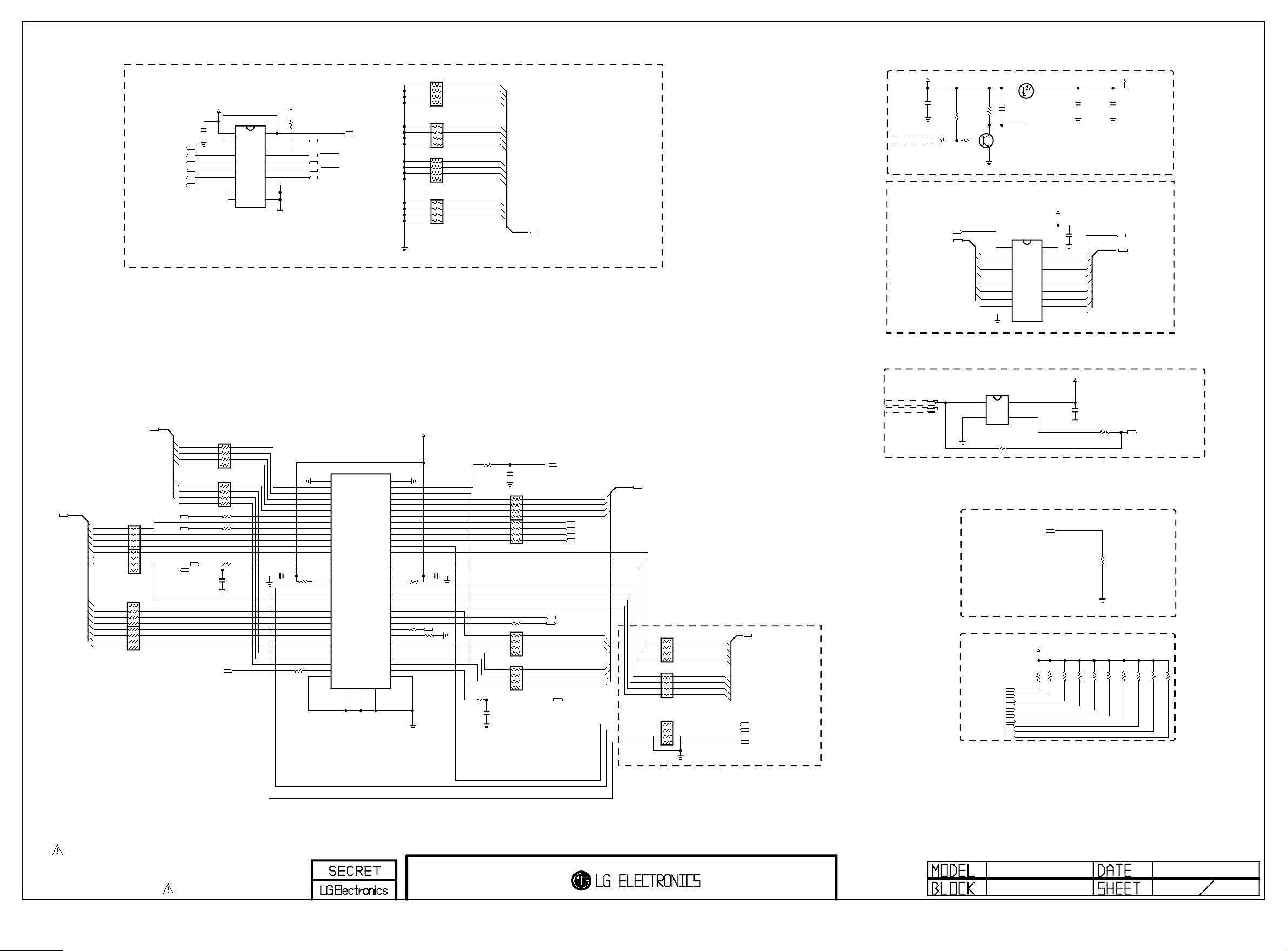
CI_A[0-14]
Copyright © 2010 LG Electronics Inc. All rights reserved.
Only for training and service purposes
LGE Internal Use Only
016:G13;016:AJ2
016:T13;016:AJ2
016:AG22
CI_A[10]
CI_A[11]
CI_A[9]
CI_A[8]
CI_A[13]
CI_A[14]
CI_A[12]
CI_A[7]
CI_A[6]
CI_A[5]
CI_A[4]
CI_A[3]
CI_A[2]
CI_A[1]
CI_A[0]
CI CONTROL BUFFER
/CI_CE1
/CI_CE2
/CI_WE
016:H12
016:T12
016:G13
016:T13
CI_D[0-7]
33
AR1304
/CI_IREQ
AR1305
33
33
AR1306
AR1307
33
/CI_IOWR
/CI_OE
/CI_IORD
CI_D[3]
CI_D[4]
CI_D[5]
CI_D[6]
CI_D[7]
CI_D[0]
CI_D[1]
CI_D[2]
/CI_CE1
/CI_OE
/CI_WE
[GP39]
007:H5;016:AJ3
[GP41]016:AJ3
+3.3V_MULTI
0.1uF
C1300
33
33
/CI_IOIS16
16V
AR1316
AR1317
C1301
MC74LCX541DTR2G
VCC
20
OE2
19
O0
18
O1
17
O2
16
O3
15
O4
14
O5
13
O6
12
O7
11
R130147
R130247
R130047
16V
0.1uF
IC1300
1
2
3
4
5
6
7
8
9
10
OE1
D0
D1
D2
D3
D4
D5
D6
D7
GND
0.1uF
+3.3V_MULTI
C1302
10K
R1303
EBI_CS
007:E7;007:E6;016:AL23
NAND_WE
EBI_WE
NAND_RE
NAND_ALE
R1305
0
R1304
100
READY
/CI_SEL
007:H5
007:C2;007:E5
007:E6
007:C3;007:E6
007:C2;007:E6
P1300
10067972-000LF
1
2
3
4
5
6
7
8
9
10
11
12
13
14
15
16
17
18
19
20
21
22
23
24
25
26 60
27 61
28 62
29 63
30 64
31
32
33
34
G1 G2
69
CI POWER ENABLE CONTROL
AR1300
10K
AR1301
10K
AR1302
10K
AR1303
10K
CI_A[0]
CI_A[1]
CI_A[2]
CI_A[3]
CI_A[4]
CI_A[5]
CI_A[6]
CI_A[7]
CI_A[8]
CI_A[9]
CI_A[10]
CI_A[11]
CI_A[12]
CI_A[13]
CI_A[14]
CI_A[0-14]
007:E7;016:C13
+5V_CI
CI_5V_CTL
007:E6
016:F16
0.1uF
C1306
16V
[GP27]007:H7
EBI_RW
CI_D[0-7]
R1312
10K
R1313
10K
B
R1314
C
E
CI_D[0]
CI_D[1]
CI_D[2]
CI_D[3]
CI_D[4]
CI_D[5]
CI_D[6]
CI_D[7]
READY
22K
Q1300
2SC3052
C1309
4.7uF
10V
DIR
A0
A1
A2
A3
A4
A5
A6
A7
GND
Q1301
RSR025P03
S
IC1301
74LVC245A
1
2
3
4
5
6
7
8
9
10
G
D
+3.3V_MULTI
VCC
20
OE
19
B0
18
B1
17
B2
16
B3
15
B4
14
B5
13
B6
12
B7
11
0.1uF
C1307
NAND_DATA[0]
NAND_DATA[1]
NAND_DATA[2]
NAND_DATA[3]
NAND_DATA[4]
NAND_DATA[5]
NAND_DATA[6]
NAND_DATA[7]
+5V_CI_Vs
C1308
22uF
10V
16VR13 18 22K
0.1uF
C1310
16V
EBI_CS
007:E7;007:E6;016:K26
NAND_DATA[0-7]
DVB-CI DETECT
+3.3V_MULTI
IC1302
NL17SZ08DFT2G
IN_B
VCC
1
FE_TS_VAL
FE_TS_ERR
+5V_CI_Vs
R1310
100
C1305
R1309
0.1uF
AR1312 33
AR1311 33
R131147
AR1310 33
AR1309 33
100
C1304
0.1uF
35
36
37
38
39
40
41
42
43
44
45
46
47
48
49
50
51
R1307
R1306
READY
READY
100
100
016:AL9
C1303
0.1uF
/CI_INPACK
R13080
52
53
54
55
56
57
58
59
65
66
67
68
/CI_CD1
CI_OUTDATA[4]
CI_OUTDATA[5]
CI_OUTDATA[6]
CI_OUTDATA[7]
007:G6;016:AJ2
CI_MOD_RESET
/CI_WAIT
CI_OUTVALID
CI_OUTSTART
CI_OUTDATA[0]
CI_OUTDATA[1]
CI_OUTDATA[2]
CI_OUTDATA[3]
[GP38]
007:H6;016:AJ3
/CI_CE2
/CI_VS1
/CI_IORD
/CI_IOWR
[GP49]
007:E6;016:AJ3
CI_OUTCLK
/CI_CD2
007:H5;016:AJ2
CI_OUTCLK,CI_OUTDATA[0-7],CI_OUTSTART,CI_OUTVALID
016:H25;016:AJ2
016:AJ3
[GP26]
016:H24
016:H25
Option For External Demod.
FE_TS_DATA[0]
FE_TS_DATA[1]
FE_TS_DATA[2]
FE_TS_DATA[3]
33
AR1313
FE_TS_DATA[4]
FE_TS_DATA[5]
FE_TS_DATA[6]
FE_TS_DATA[7]
AR1314 33
AR1315
33
FE_TS_DATA[0-7]
FE_TS_SYNC
FE_TS_VAL_ERR
FE_TS_DATA_CLK
DVB-CI PULL-UP (Near CI Slot)
016:I8
007:H5;016:G11
016:T13
007:E6;016:S10
007:H5;016:V14
007:H6;016:S15
007:H5;016:S7
016:G13;016:H26
016:H25;016:T13
007:G6;016:S10
5
IN_A
2
READY
OUT_Y
GND
4
3
READY
C1311
0.1uF
16V
GND
R1326
0
DVB-CI PULL-DOWN (Near CI Slot)
/CI_INPACK
016:O9
External Demod.
+5V_CI
10K
READY
/CI_IOIS16
/CI_IREQ
/CI_VS1
/CI_WAIT
CI_OUTCLK
/CI_CD1
/CI_CD2
/CI_CE1
/CI_CE2
CI_MOD_RESET
R1315
R1316 10K
READY
R1317 10K
READY
R1319 10K
READY
R1327
0
10K
R1320
FE_TS_VAL_ERR
READY
READY
READY
R1323 10K
R1321 10K
R1324 10K
R1322 10K
R1325 10K
THE SYMBOL MARK OF THIS SCHEMETIC DIAGRAM INCORPORATES
SPECIAL FEATURES IMPORTANT FOR PROTECTION FROM X-RADIATION.
FILRE AND ELECTRICAL SHOCK HAZARDS, WHEN SERVICING IF IS
ESSENTIAL THAT ONLY MANUFATURES SPECFIED PARTS BE USED FOR
THE CRITICAL COMPONENTS IN THE SYMBOL MARK OF THE SCHEMETIC.
DVB-CI SLOT
BCM3556-C0
DVB-CI SLOT
10/01
5 13
Page 25

Page 26
PDP TV Repair Process Index
- Trouble shooting by worst symptom
No. Symptom (L) Symptom (M) Page Remark
1
2 No Picture/No sound 2
3 Mal-discharge/Noise/dark picture 3
4 Picture broken/Freezing 4
5 Vertical bar/ Horizontal Bar 5
6
7 Turn off (Instant, under watching) 7
8 C. Sound Problem No sound/ Sound distortion 8
9 E. General function Problem Remote control & Local switch checking 9
A. Picture Problem
B. Power Problem
No Picture/Sound OK 1
No Power (Not turn on) 6
First of all, Check whether there is SVC Bulletin in GCSC System for these model.
ⓒ LG Electronics. Inc.2009
Page 27
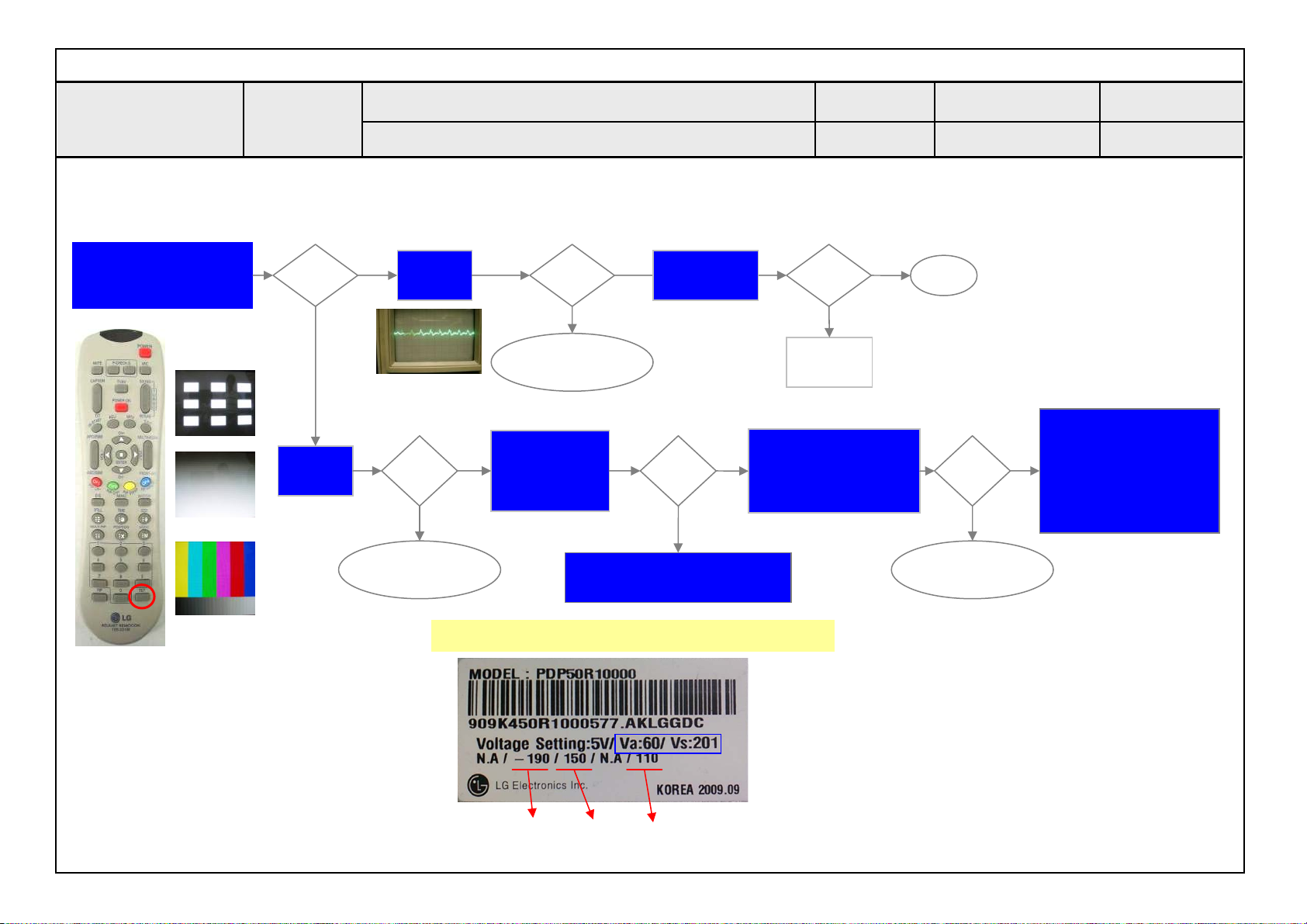
Repair Process
PDP TV
Symptom
A. Picture Problem
No Picture/Sound OK
Making
Revision
2010. 2 . 22
First of all, Check whether all of cable between board was inserted properly or not.
(Main B/D↔ Power B/D, Power B/D↔ Y-sus B/D,Y-Sus B/D ↔Z-Sus B/D,LVDS Cable,Speaker Cable,IR B/D Cable,,,)
Check Module pattern
by using “TILT” key
on SVC R/C
Normal
N
Check
Vs, Va
Check
Y
Sound
Normal
N
Move
Power problem
Section
Sound
Move
No Picture/No sound
Section
Check voltage
Y
. -V
Y
. VSC
. VZB
Y
OK
N
1. Check Y-Sus/ Z-Sus Board
2. Replace defective B/D
Check
LVDS Cable
Normal Normal
Y
N
Normal
N
Replace
Main B/D
Check B+ Voltage
on Power Board
/ Control Board
.Check B+(5V)
Y
Close
Power problem
Y
N
Move
Section
전자 -6-2
1/9
1.Check Control Board
. LED on
. Crystal(X101)
. 1.8V, 3V, 5V FET
. Rom update
2.Replace Control B/D
<SVC R/C & Pattern>
※Refer to the Module label for each voltage
-VY VSC VZB
ⓒ LG Electronics. Inc.2009
Page 28
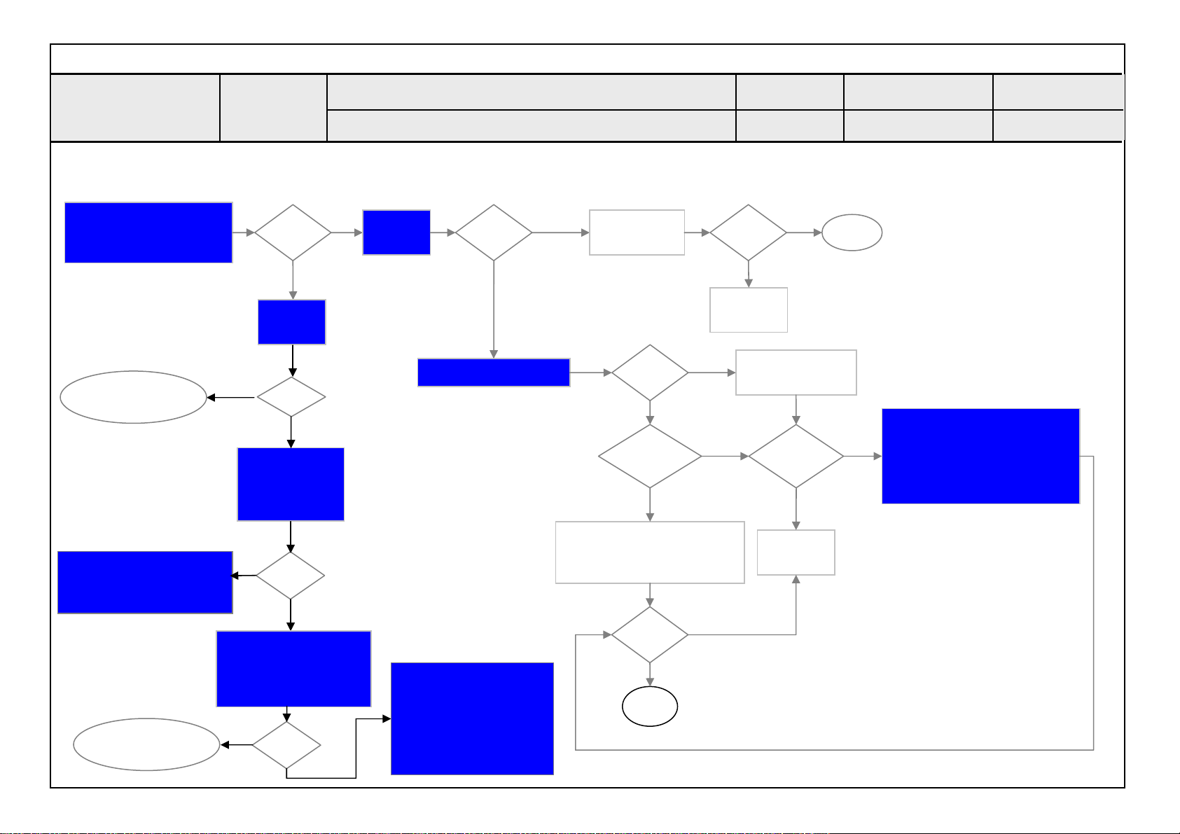
Repair Process
PDP TV
Check Module pattern
by using “TILT” key
on SVC R/C
Move
Power problem
Section
1. Check Y-Sus/ Z-Sus
Board
2. Replace defective B/D
Move
Power problem
Section
Symptom
Normal
N
Check
Vs, Va
N
Normal
Y
Check voltage
. -V
Y
. VSC
. VZB
N
Normal
Y
Check B+ Voltage
on Power Board
/ Control Board
.Check B+(5V)
N
Normal
A. Picture Problem
No Picture/No Sound
Check
Y
Sound
1.Check Control Board
. LED on
. Crystal(X101)
. 1.8V, 3V, 5V FET
. Rom update
Y
2.Replace Control B/D
Sound
OK
N
Check IR operation
Y
(Firmware Management)
Check
LVDS Cable
Normal
Y
Power
LED ON?
N
Latest S/W update
from GCSC
Normal
Y
Close
2
N
N
Making
Revision
Normal
N
Replace
Main B/D
Repair/Replace
Y
appear?
Replace
Main B/D
Y
IR B/D
OSD
2010. 2 . 22
Close
Check Input signal
. RF Cable connection
Y
. SCART Cable connection
. HDMI Cable connection
N
. Component Cable …
ⓒ LG Electronics. Inc.2009
전자 -6-2
2/9
Page 29
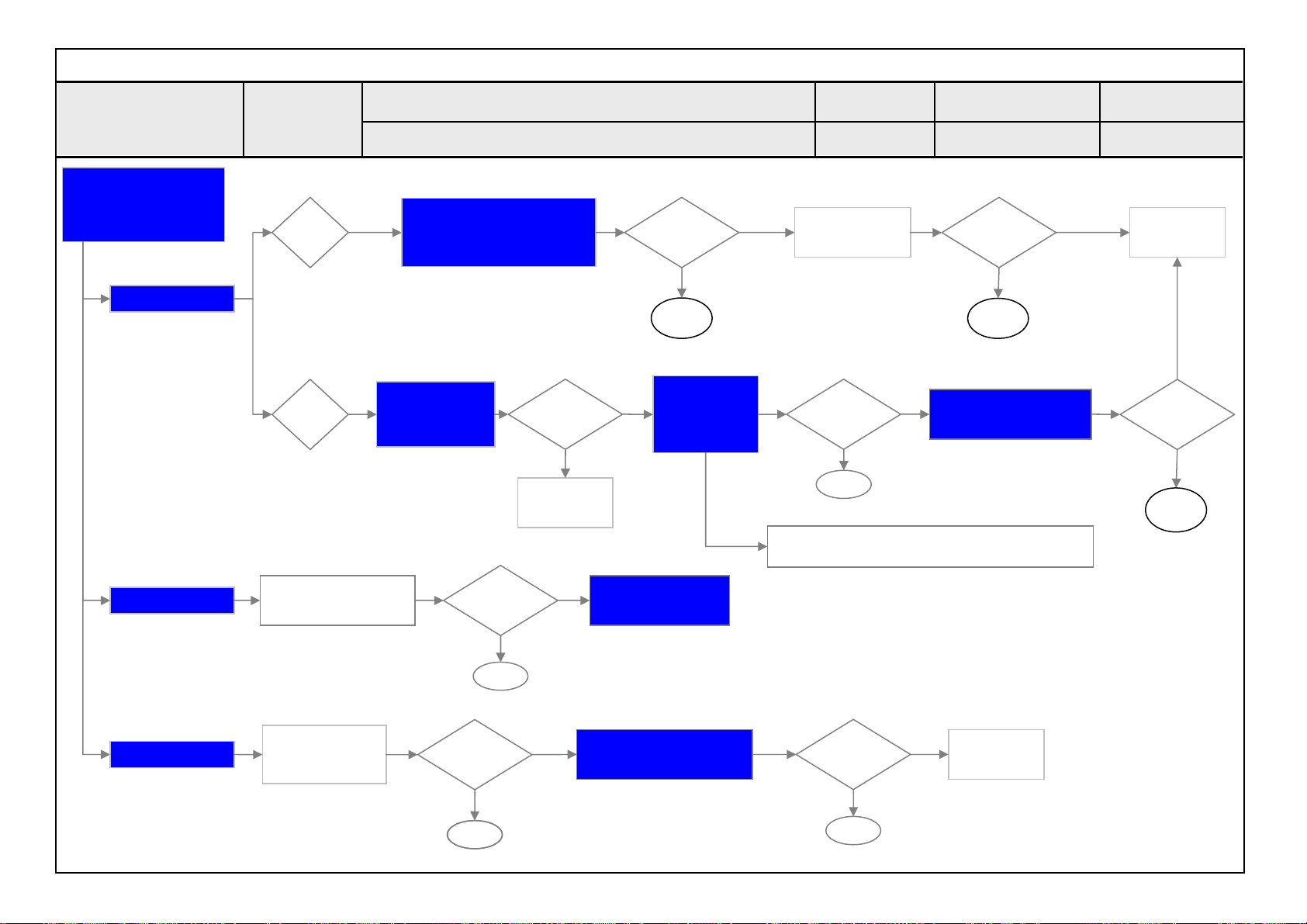
Repair Process
PDP TV
Check
Picture problem
Type
Mal-discharge
Symptom
Dot
type
Scan
Type
A. Picture Problem
Mal-discharge/Noise/dark picture
Check CTRL ROM Ver.
and
Rom Upgrade
Check voltage
. –V
Y / VSC
(Y-Sus B/D)
Normal
Picture?
N
Replace
Y-Sus B/D
Normal
Picture?
Close
Y
Y Drive B/D
Replace B/D
Y
Check
&
Making
2010. 2 . 22
Revision
N
※Check Discharge resistance (10Ω 2~3ea)
Replace
Control board
Normal
Picture?
Y
Close
on Power B/D before replace Y Drive B/D
N
Normal
Picture?
Y
Close
1.Check Control B/D
2.Replace Board
N
전자 -6-2
3/9
Replace
Module
N
Normal
Picture?
Y
Close
Picture Noise
Dark Picture
Check RF Cable
Connection
Check
Picture mode
setting
Normal
Picture?
Close
Normal
Picture?
Y
Close
N
Check Tuner
& Replace
Y
N
1. Check Z-Sus Board
2. Replace Board
Normal
Picture?
Y
Close
3
N
Replace
Module
ⓒ LG Electronics. Inc.2009
Page 30
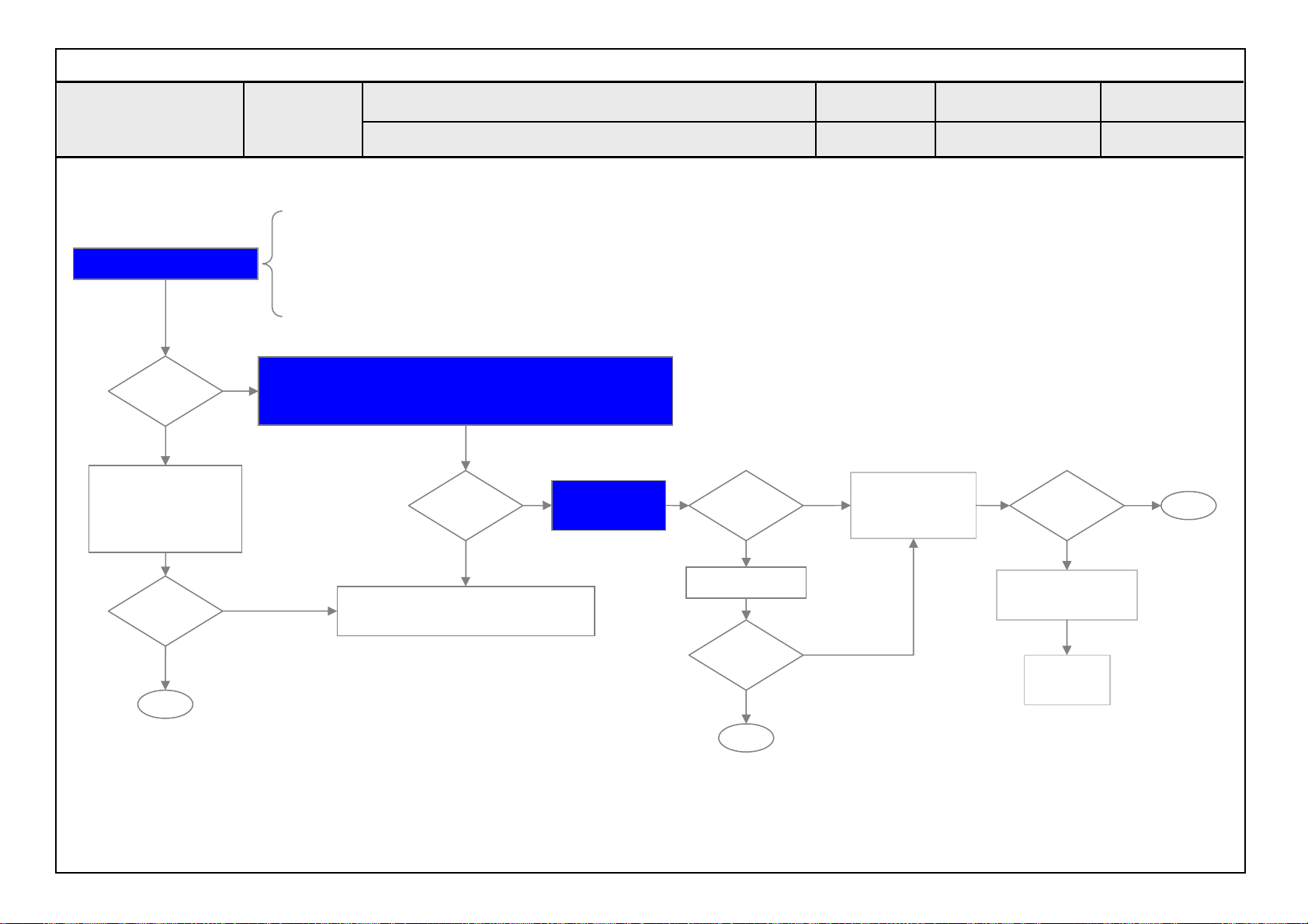
Repair Process
PDP TV
Check RF Signal level
Normal
Signal?
N
Check RF Cable
Connection
1. Reconnection
2. Install Booster
Normal
Picture?
Y
Close
Y
N
Symptom
A. Picture Problem
Picture broken/Freezing
. By using Digital signal level meter
. By using Diagnostics menu on OSD
( Menu→Press Red Key on R/C→Enter Signal Test)
- Signal strength (Normal : over 50%)
- Signal Quality (Normal: over 50%)
Check whether other equipments have problem or not.
(By connecting RF Cable at other equipment)
→ DVD Player ,Set-Top-Box, Different maker TV etc
Normal
Picture?
N
Contact with signal distributor
or broadcaster (Cable or Air)
Y
Check
S/W Version
SVC
Bulletin?
Y
S/W Upgrade
Normal
Picture?
Y
Making
2010. 2 . 22
Revision
■ Menu→Setup →Booster
N
Booster menu
On→Off: Check
Off→On: Check
N
Normal
Picture?
N
Check
Tuner soldering
Replace
Main B/D
전자 -6-2
4/9
Y
Close
Close
4
ⓒ LG Electronics. Inc.2009
Page 31
Repair Process
PDP TV
Check
defect type
Vertical
Line/Bar
Symptom
Regular
Vertical
Line / Bar
Irregular
Vertical
Line / Bar
A. Picture Problem
Vertical bar/ Horizontal Bar
Check Module pattern
by using “TILT” key
on SVC R/C
Check connection
of Connector
(COF,TCP)
on CTRL B/D , X B/D
1.Connector re-connection
2.Eliminate foreign material on Connector
Normal
N
Pattern?
1.Check CTRL B/D
2.Replace Board
Y
1.Check CTRL B/D
2.Replace Board
Normal
N
Making
2010. 2 . 22
Revision
Y
Replace
Module
※CTRL B/D: Control board
Normal
Picture?
Y
Close
N
전자 -6-2
5/9
Check Main B/D
Replace Module
(If Main B/D doesn’t cause)
Half
No picture
Horizontal
Line/Bar
1.Check X B/D
2.Replace Board
Check connection
of Connector (FPC)
on Y Drive B/D
1.Connector re-connection
2.Eliminate foreign material on FPC
Picture?
Normal
N
Normal
Y
Close
Y
N
1. Check Y Drive B/D
2. Replace Board
Replace
Module
※ H-Line’s Cause is rare CTRL B/D
N
Normal
Picture?
Y
Close
1.Check CTRL B/D
2.Replace Board
5
Normal
Picture?
Close
ⓒ LG Electronics. Inc.2009
N
Replace
Module
Y
Page 32
Repair Process
PDP TV
Check
Power LED
. Stand-By: Red
. Operating: Green
Check Power cord
was inserted properly
Mechanical Power switch
on Local control of TV
Symptom
Power LED
ON?
N
Check & Repair
Normal
?
N
B. Power Problem
No Power (Not turn on)
DC Power on
Y
by pressing Power Key
On Remote control
Y
Close
Normal
Close
N
Y
Check
R/C IR Operation
Making
Revision
Normal
2010. 2 . 22
Y
N
Repair/Replace
IR B/D
전자 -6-2
6/9
Check ST-BY 5V
on Power Board
Normal
Voltage?
Y
N
Check
AC DET Signal
on Power B/D
Normal
Signal?
N
Check Power B/D
Replace Power B/D
Y
Check
RL_ON Signal
on Power B/D
6
Normal
Signal?
N
Check Main B/D
Replace Main B/D
Y
the other pin’s
Output voltage
on Power B/D
Check
N
Normal
Y
Close
ⓒ LG Electronics. Inc.2009
Replace
Power B/D
Page 33
Repair Process
PDP TV
Symptom
※ To check Power B/D Protection
Instant
Turn off
Turn off
Under watching
Turn on after pull out connector
between Power B/D & Y-Sus
“Off Timer”
“Off timer”
Function off
Set?
B. Power Problem
Turn off (Instant, under watching)
Power LED
Green?
N
Check Power B/D
Replace Power B/D
N
Y
Check
Power Off History
Power Off History
Y
RCU Off
KEY Off
2HOUR Off
NO Signal Off
Don’t appear
Making
2010. 2 . 22
Revision
1. Check Y-Sus/ Z-Sus Board
(especially Short or Open)
2. Replace defective B/D
This is not problem
Normal operation
Move
No Power problem
Section
전자 -6-2
7/9
7
ⓒ LG Electronics. Inc.2009
Page 34
Repair Process
PDP TV
1.No sound( If HDMI Input only have no sound, download EDID data)
Check
“Speaker ON/Off” setting
in OSD Menu
2.Sound distortion & sound drop
Check Input signal
→Cable connection
→Cable open
-RF & external
(HDMI,SCART,,,)
Symptom
Normal
Sound?
Y
Close
Normal
Sound?
Y
Close
N
No sound/ Sound distortion
N
AVL off/on
Clear voiceⅡ off/on
Check Speaker
jack connection
& Speaker Cable open
Check
Normal
Sound?
Y
Close
C. Sound Problem
Normal
Sound?
Close
N
Making
Revision
N
Y
Problem in all input
Problem in only DTV(Case 1)
Problem in external input(Case 2)
(SCART,HDMI,,,)
SVC
Bulletin?
N
Check 17V
(Audio IC B+)
on Power B/D
Y
Check Audio IC Short
Replace Main B/D
2010. 2 . 22
Apply
SVC Bulletin
(S/W Upgrade etc)
Normal
voltage?
N
Y
전자 -6-2
8/9
Close
Normal
Sound?
N
Check Power B/D
Replace Power B/D
Y
Check whether Problem happen
in same output of other equipments or not.
(By connecting same output cable of other equipment)
→ DVD Pla y er ,Set-Top-Box, different maker TV etc
Cause is RF Signal’s problem (Case 1)
Cause is Equipment’s problem (case 2)
Normal
Sound?
Y
Explain customer that
8
N
SVC
Bulletin?
Y
Apply
SVC Bulletin
(S/W Upgrade etc)
ⓒ LG Electronics. Inc.2009
Normal
Sound?
Check Audio IC
Replace Main B/D
Y
NN
Close
Page 35
Repair Process
PDP TV
1. Remote controller (R/C) operating error
Check R/C itself
Operation
Check R/C Operating
When turn off light
in room
If R/C operate,
Explain the customer
cause is interference
from light in room.
Symptom
Normal
operating?
N
Check & Replace
Battery of R/C
Replace R/C
Y
Normal
operating?
N
Remote control & Local switch checking
Check & Repair
Cable connection
Connector solder
Close
D. General Function Problem
Normal
operating?
Y
Close
N
Check B+ 5V
On Main B/D
(Power B/D don’t have problem)
Making
Revision
Normal
Voltage?
Check 5v on Power B/D
Replace Power B/D or
Replace Main B/D
Y
N
2010. 2 . 22
Check IR
Output signal
전자 -6-2
Replace
Main B/D
Normal
Signal?
N
Repair/Replace
IR B/D
9/9
Y
2. Local (Mechanical) switch operating error
Check R/C
Operation
Normal
operating?
N
Move
Power problem
Section
Y
Check & Repair
Cable connection
Connector solder
Normal
operating?
Y
Close
Replace
Main B/D
N
Check & Replace
Assembly status
(Key PCB + tool )
9
Normal
operating?
Y
Close
N
Output signal
Check Key
Repair/Replace
Local switch B/D
ⓒ LG Electronics. Inc.2009
Normal
Signal?
N
Y
Page 36
PDP TV Repair Process Index
- Trouble shooting by input block (Component level check)
No. Symptom (L) Input Block Page Remark
1 Power Problem Power-up Boot fail 1
2
3 Analog TV 3
4 Component 4
Video Probelm
5 RGB(D-SUB) 5
6 AV(Scart / CVBS) 6
7 HDMI 7
8
9 Digital TV / HDMI 9
10 Analog TV 10
11 Component / AV / RGB 11
12 Optical Audio 12
Audio Problem
Digital TV 2
All Input 8
13 No USB All Input 13
14USB ProblemUSB Problem14
15 Bluetooth Problem Bluetooth Problem 15
ⓒ LG Electronics. Inc.2009
Page 37
PDP TV
Symptom
Power-Up Boot Fail
Making
Revision
2010. 2 . 22
전자 -6-2
1/15
Check P500 All
Voltage Level (17V, 5V)
Y
Check IC503 (pin2) Output
Voltage Level (2.5V)
Y
Check L507
Voltage Level 1.2V
Y
Check IC505 (pin2)
Voltage Level 3.3V
N
N
N
N
Check Power connector
OK ?
Replace IC503
Replace L507
Replace IC505
Y
Replace Power board
ⓒ LG Electronics. Inc.2009
Page 38
PDP TV
Input
Block
Check RF Cable
Y
Check TU601 Power
5V(C509), 3.3V(L602),
2.5V(L601),1.2V(L600)
Y
Digital TV Video Problem
Check Voltage
N
5V : IC503 Output
3V : IC505 Output
2.5V : IC503 Output
1.2V:IC601 Output
Making
Revision
2010. 2 . 22
전자 -6-2
2/15
ⓐ
Check Video color
Y
Check IIC Line Check SCL/SDA1 Line
Y
Check TP Clock, Data, Sync
Y
Check other input / OSD
Y
Change BCM(IC100)
N
N
N
N
Check Monitor Out Video
(Scart out)
Y
Go to ⓐ
Maybe Tuner has problems
: Replace Tuner
Check Module
N
Replace Tuner
ⓒ LG Electronics. Inc.2009
Page 39
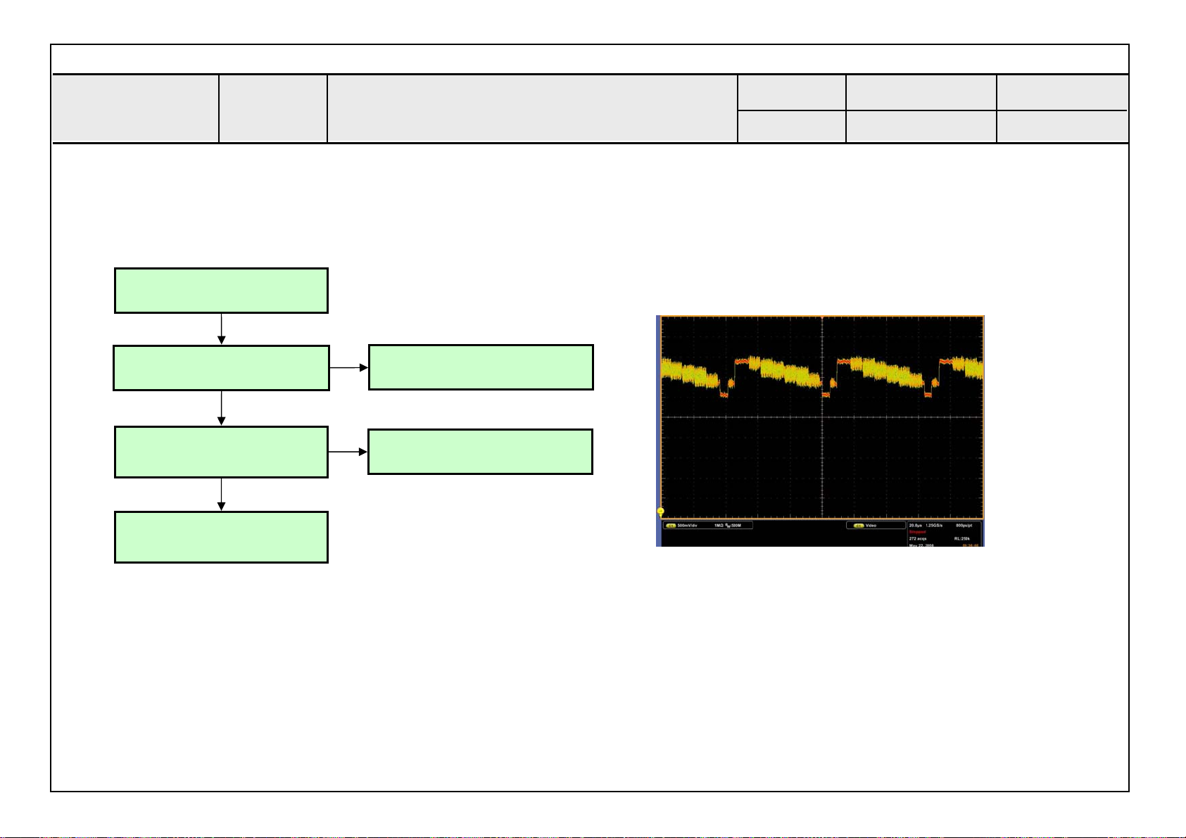
PDP TV
Input
Block
Check RF Cable
Y
Analog TV Video Problem
Making
Revision
2010. 2 . 22
전자 -6-2
3/15
Check 5V voltage
on TU601(Pin3)
Y
Check CVBS signal
TU601 #11 Pin
Y
Replace BCM(IC100)
N
N
Check IC503 Output
Voltage(L502)
Replace Tuner(TU601)
< CVBS waveform – sample >
- Defend on the input signal.
ⓒ LG Electronics. Inc.2009
Page 40
PDP TV
Check input signal format
Check Component Cable
Input
Block
Is it supported?
Y
Y
Component Video Problem
Making
Revision
2010. 2 . 22
전자 -6-2
4/15
Check signal
on C338,C339,C340
Y
Replace BCM(IC100)
N
Check the damage of JK1000
And Replace Connector
※ Measured signals depend on the input signal.
ⓒ LG Electronics. Inc.2009
Page 41
PDP TV
Check input signal format
conductors for damage
Input
Block
Is it supported?
Y
Check RGB Cable
Y
Check P900 Replace connector (P900).
Y
RGB(D-Sub) Video Problem
N
Making
Revision
2010. 2 . 22
전자 -6-2
5/15
Check signal, Hsync, Vsync
R953, R959
Y
Check signal
C332, C333, C334
Y
Replace Mstar(IC100)
N
Check IC903 Input/Output
N
Replace C332, C333, C334
※ Measured signals depend on the input signal.
ⓒ LG Electronics. Inc.2009
Page 42
PDP TV
Check AV Cable for damage or open
Check AV port of JK1002(Side),
Input
Block
Check input signal format
Is it supported?
Y
conductors
Y
JK1001(Rear)
Y
AV Video Problem
N
Replace connector
Making
Revision
2010. 2 . 22
전자 -6-2
6/15
Check signal line
JK1002-Video : R359
JK1001-Video : C432,C433,C434(RGB),
C326(CVBS)
Y
Replace BCM(IC100)
N
Replace Resistor or Cap
※ Measured signals depend on the input signal.
ⓒ LG Electronics. Inc.2009
Page 43
PDP TV
Check HDMI Cable for damage or
Input
Block
Check input signal format
Is it supported?
Y
open conductors
Y
Check EDID D/L Re-Download EDID
Y
HDMI Video Problem
N
Making
Revision
2010. 2 . 22
전자 -6-2
7/15
Check JK800 / J801 / J802
for proper connection or damage
Y
Check R867~R874
(HDMI Switch Output)
Y
Replace BCM(IC100)
N
N
Replace Connector
Replace IC802
ⓒ LG Electronics. Inc.2009
Page 44
PDP TV
Make sure you can’t hear any audio
Input
Block
Y
Check speaker for damage. Replace the Speaker
Y
All Input Audio Problem
N
Making
Revision
2010. 2 . 22
전자 -6-2
8/15
Check Connector
P1000
Y
Check IC700 Power
17V(L704), 3.3V(L702,L703)
Y
Check IC700 Status
PDN(#19) / Reset(#25) is High?
Y
Check SCL,SDA
R707, R708
Y
Check BCM I2S Output
R114, #21, 22, 23 on IC700
Y
Replace AMP(IC700)
N
N
N
N
N
Replace P1000
Check 17V (P500 #1,2),
3.3V (IC505 #2)
Check
Reset (R704) / PDN (R702)
:They must be High (3.3V)
Replace R707, 708
Replace BCM(IC100).
ⓒ LG Electronics. Inc.2009
Page 45
PDP TV
◆ Digital TV
Input
Block
Digital TV / HDMI Audio Problem
Making
Revision
2010. 2 . 22
전자 -6-2
9/15
Check video output
Y
Follow procedure All source audio
trouble shooting
◆ HDMI
Check video output
Y
Check EDID Download Re-download EDID data
Y
N
N
N
Follow procedure digital TV
video trouble shooting
Follow procedure HDMI video
trouble shooting
Follow procedure All source audio
trouble shooting
ⓒ LG Electronics. Inc.2009
Page 46
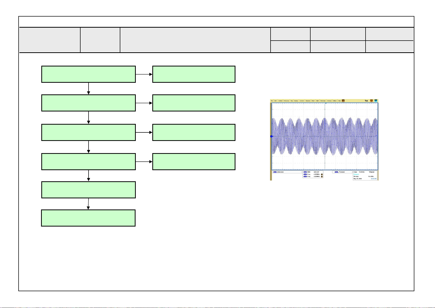
PDP TV
Input
Block
Analog TV Audio Problem
Making
Revision
2010. 2 . 22
전자 -6-2
10/15
Check video output
Y
Check #2 on TU601 for 5V Check IC504 output Voltage
Y
Check SIF signal C602 Replace TU601
Y
Check SIF signal (C301) Check SIF line
Y
Follow procedure All source audio
trouble shooting
Y
Replace BCM IC (IC100)
N
N
N
N
Follow procedure analog TV
video trouble shooting
< SIF waveform – sample >
- Defend on the input signal.
ⓒ LG Electronics. Inc.2009
Page 47
PDP TV
JK1000 (Component) : R1005, R1006
JK1000 (Component) : R209, R210
Input
Block
Check Connector and ca bles
JK1000 (Component)
JK1001 (SCART)
JK702 (RGB)
JK900 (Side AV)
Y
Check signal
JK1001 (SCART) : R1024, R1025
JK702 (RGB) : R931, R933
JK900 (Side AV) : R1039, R1040
Y
Check IC100 signal
JK1001 (SCART) : R212, R213
JK702 (RGB) : R216, R217
JK900 (Side AV) : R214, R215
Component / AV/RGB Audio Problem
Making
2010. 2 . 22
Revision
N
N
N
Replace connector or
cable if found damaged
Replace the Resistor
Replace the Resistor
전자 -6-2
11/15
Y
Follow procedure
All source audio trouble shooting
ⓒ LG Electronics. Inc.2009
Page 48
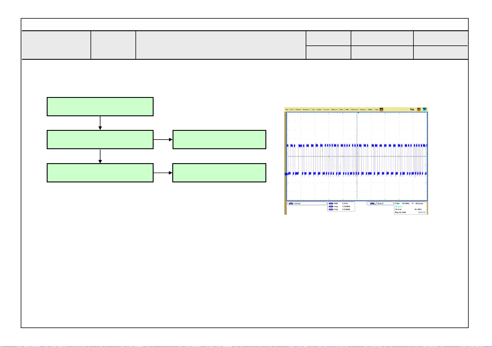
PDP TV
Check Signal (JK1000 #3)
Check SPDIF signal (R1051) Replace BCM(IC100)
Input
Block
Y
Check 5V #2 on JK1003
Y
Optical Audio Problem
N
Check Q501 Output (L516)
N
Making
Revision
2010. 2 . 22
전자 -6-2
12/15
< SPDIF waveform – sample >
- Defend on the input signal.
ⓒ LG Electronics. Inc.2009
Page 49
PDP TV
Input
Block
No OSD( or Picture) Problem
Making
Revision
2010. 2 . 22
전자 -6-2
13/15
Check LED blanking
When press a key on R/C
Y
Check Vs,Va, 5V,17V
on Power Board
Y
Check DISP_EN(R253) Check R27 and MICOM
Y
Check LVDS Cable damage
or open connectors.
Y
Check LVDS DATA
Y
N
N
N
N
N
Follow Power-Up Boot Fail
Replace Power Board
Replace Cable
Change BCM(IC100)
Check Module condition
ⓒ LG Electronics. Inc.2009
Page 50
PDP TV
Check USB 2.0 Cable for damage
Input
Block
or open conductors
Y
USB Problem
Making
Revision
2010. 2 . 22
전자 -6-2
14/15
Check P1101/P1102 Replace Connector
Y
Check C1116/C1117 voltage 5V
Y
Check R1133,R1134,R1137,R1138
Y
Check R200,R201
Y
Change BCM(IC100)
N
N
N
N
Check IC1102/1103 #8 status
is high ?
N
Replace Capacitor
Replace the Resistor
Replace IC1100
Y
Y
Check USB Module condition
ⓒ LG Electronics. Inc.2009
Page 51
PDP TV
Input
Block
Check B/T Version
on INSTART MENU
N
Bluetooth Problem
Making
Revision
2010. 2 . 22
전자 -6-2
13/15
Check #10 P1100 is 3.3V Replace Connector
Y
Check R204, R205
Y
Change BCM(IC100)
N
N
Check P1100
N
Replace Bluetooth Module
ⓒ LG Electronics. Inc.2009
 Loading...