

LG 50LN5710, 50LN5750 Schematic
Internal Use Only
North/Latin America http://aic.lgservice.com
Europe/Africa http://eic.lgservice.com
Asia/Oceania http://biz.lgservice.com
LED TV
SERVICE MANUAL
CHASSIS : LA33B
MODEL : 50LN5750/5710
50LN5750-UH/5710-UI
CAUTION
BEFORE SERVICING THE CHASSIS,
READ THE SAFETY PRECAUTIONS IN THIS MANUAL.
Printed in KoreaP/NO : MFL67727557(1305-REV01)

CONTENTS
CONTENTS .............................................................................................. 2
PRODUCT SAFETY ................................................................................. 3
SPECIFICATION ....................................................................................... 4
ADJUSTMENT INSTRUCTION .............................................................. 13
EXPLODED VIEW .................................................................................. 23
SCHEMATIC CIRCUIT DIAGRAM ..............................................................
Only for training and service purposes
- 2 -
LGE Internal Use OnlyCopyright © LG Electronics. Inc. All rights reserved.
SAFETY PRECAUTIONS
IMPORTANT SAFETY NOTICE
Many electrical and mechanical parts in this chassis have special safety-related characteristics. These parts are identified by in the
Schematic Diagram and Exploded View.
It is essential that these special safety parts should be replaced with the same components as recommended in this manual to prevent
Shock, Fire, or other Hazards.
Do not modify the original design without permission of manufacturer.
General Guidance
An isolation Transformer should always be used during the
servicing of a receiver whose chassis is not isolated from the AC
power line. Use a transformer of adequate power rating as this
protects the technician from accidents resulting in personal injury
from electrical shocks.
It will also protect the receiver and it's components from being
damaged by accidental shorts of th e cir cuitry that may be
inadvertently introduced during the service operation.
If any fuse (or Fusible Resistor) in this TV receiver is blown,
replace it with the specified.
When replacing a high wattage resistor (Oxide Metal Film Resistor,
over 1 W), keep the resistor 10 mm away from PCB.
Keep wires away from high voltage or high temperature parts.
Before returning the receiver to the customer,
always perform an AC leakage current check on the exposed
metallic parts of the cabinet, such as antennas, terminals, etc., to
be sure the set is safe to operate without damage of electrical
shock.
Leakage Current Cold Check(Antenna Cold Check)
With the instrument AC plug removed from AC source, connect an
electrical jumper across the two AC plug prongs. Place the AC
switch in the on position, connect one lead of ohm-meter to the AC
plug prongs tied together and touch other ohm-meter lead in turn to
each exposed metallic parts such as antenna terminals, phone
jacks, etc.
If the exposed metallic part has a return path to the chassis, the
measured resistance should be between 1 MΩ and 5.2 MΩ.
When the exposed metal has no return path to the chassis the
reading must be infinite.
An other abnormality exists that must be corrected before the
receiver is returned to the customer.
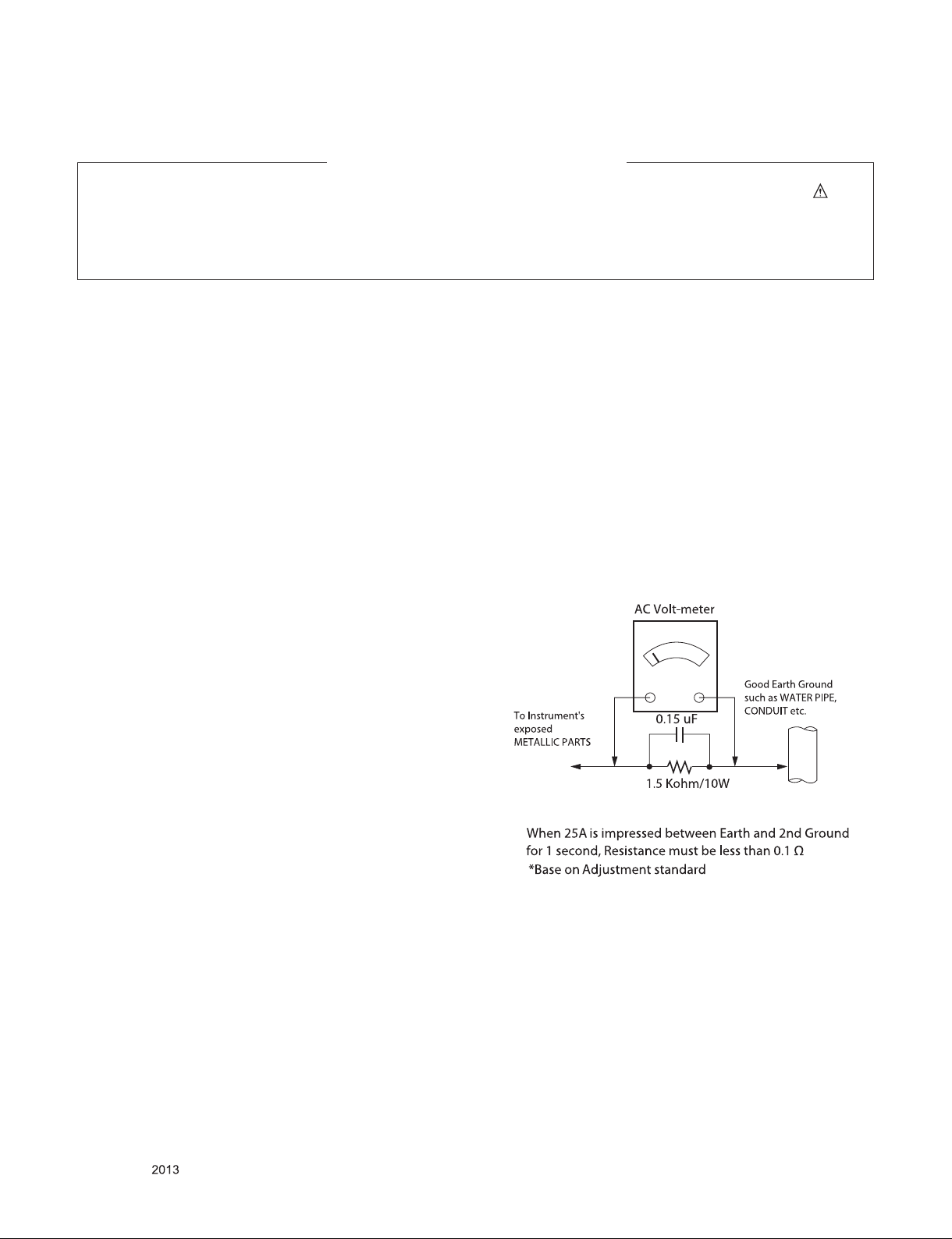
Leakage Current Hot Check (See below Figure)
Plug the AC cord directly into the AC outlet.
Do not use a line Isolation Transformer during this check.
Connect 1.5 K / 10 watt resistor in parallel with a 0.15 uF capacitor
between a known good earth ground (Water Pipe, Conduit, etc.)
and the exposed metallic parts.
Measure the AC voltage across the resistor using AC voltmeter
with 1000 ohms/volt or more sensitivity.
Reverse plug the AC cord into the AC outlet and repeat AC voltage
measurements for each exp ose d metallic par t. Any voltage
measured must not exceed 0.75 volt RMS which is corresponds to
0.5 mA.
In case any measurement is out of the limits specified, there is
possibility of shock hazard and the set must be checked and
repaired before it is returned to the customer.
Leakage Current Hot Check circuit
Only for training and service purposes
- 3 -
LGE Internal Use OnlyCopyright © LG Electronics. Inc. All rights reserved.

SERVICING PRECAUTIONS
CAUTION: Before servicing receivers covered by this service
manual and its supplements and addenda, read and follow the
SAFETY PRECAUTIONS on page 3 of this publication.
NOTE: If unforeseen circumstances create conict between the
following servicing precautions and any of the safety precautions
on page 3 of this publication, always follow the safety precautions.
Remember: Safety First.
General Servicing Precautions
1. Always unplug the receiver AC power cord from the AC power
source before;
a. Removing or reinstalling any component, circuit board mod-
ule or any other receiver assembly.
b. Disconnecting or reconnecting any receiver electrical plug or
other electrical connection.
c. Connecting a test substitute in parallel with an electrolytic
capacitor in the receiver.
CAUTION: A wrong part substitution or incorrect polarity
installation of electrolytic capacitors may result in an explosion hazard.
2. Test high voltage only by measuring it with an appropriate
high voltage meter or other voltage measuring device (DVM,
FETVOM, etc) equipped with a suitable high voltage probe.
Do not test high voltage by "drawing an arc".
3. Do not spray chemicals on or near this receiver or any of its
assemblies.
4. Unless specied otherwise in this service manual, clean
electrical contacts only by applying the following mixture to the
contacts with a pipe cleaner, cotton-tipped stick or comparable
non-abrasive applicator; 10 % (by volume) Acetone and 90 %
(by volume) isopropyl alcohol (90 % - 99 % strength)
CAUTION: This is a ammable mixture.
Unless specied otherwise in this service manual, lubrication of
contacts in not required.
5. Do not defeat any plug/socket B+ voltage interlocks with which
receivers covered by this service manual might be equipped.
6. Do not apply AC power to this instrument and/or any of its
electrical assemblies unless all solid-state device heat sinks are
correctly installed.
7. Always connect the test receiver ground lead to the receiver
chassis ground before connecting the test receiver positive
lead.
Always remove the test receiver ground lead last.
8. Use with this receiver only the test xtures specied in this
service manual.
CAUTION: Do not connect the test xture ground strap to any
heat sink in this receiver.
Electrostatically Sensitive (ES) Devices
Some semiconductor (solid-state) devices can be damaged easily by static electricity. Such components commonly are called
Electrostatically Sensitive (ES) Devices. Examples of typical ES
devices are integrated circuits and some eld-effect transistors
and semiconductor “chip” components. The following techniques
should be used to help reduce the incidence of component damage caused by static by static electricity.
1. Immediately before handling any semiconductor component or
semiconductor-equipped assembly, drain off any electrostatic
charge on your body by touching a known earth ground. Alternatively, obtain and wear a commercially available discharging
wrist strap device, which should be removed to prevent potential shock reasons prior to applying power to the unit under test.
2. After removing an electrical assembly equipped with ES
devices, place the assembly on a conductive surface such as
aluminum foil, to prevent electrostatic charge buildup or exposure of the assembly.
3. Use only a grounded-tip soldering iron to solder or unsolder ES
devices.
4. Use only an anti-static type solder removal device. Some solder
removal devices not classied as “anti-static” can generate
electrical charges sufcient to damage ES devices.
5. Do not use freon-propelled chemicals. These can generate
electrical charges sufcient to damage ES devices.
6. Do not remove a replacement ES device from its protective
package until immediately before you are ready to install it.
(Most replacement ES devices are packaged with leads electrically shorted together by conductive foam, aluminum foil or
comparable conductive material).
7. Immediately before removing the protective material from the
leads of a replacement ES device, touch the protective material
to the chassis or circuit assembly into which the device will be
installed.
CAUTION: Be sure no power is applied to the chassis or circuit,
and observe all other safety precautions.
8. Minimize bodily motions when handling unpackaged replacement ES devices. (Otherwise harmless motion such as the
brushing together of your clothes fabric or the lifting of your
foot from a carpeted oor can generate static electricity sufcient to damage an ES device.)
General Soldering Guidelines
1. Use a grounded-tip, low-wattage soldering iron and appropriate
tip size and shape that will maintain tip temperature within the
range or 500 °F to 600 °F.
2. Use an appropriate gauge of RMA resin-core solder composed
of 60 parts tin/40 parts lead.
3. Keep the soldering iron tip clean and well tinned.
4. Thoroughly clean the surfaces to be soldered. Use a mall wirebristle (0.5 inch, or 1.25 cm) brush with a metal handle.
Do not use freon-propelled spray-on cleaners.
5. Use the following unsoldering technique
a. Allow the soldering iron tip to reach normal temperature.
(500 °F to 600 °F)
b. Heat the component lead until the solder melts.
c. Quickly draw the melted solder with an anti-static, suction-
type solder removal device or with solder braid.
CAUTION: Work quickly to avoid overheating the circuit
board printed foil.
6. Use the following soldering technique.
a. Allow the soldering iron tip to reach a normal temperature
(500 °F to 600 °F)
b. First, hold the soldering iron tip and solder the strand against
the component lead until the solder melts.
c. Quickly move the soldering iron tip to the junction of the
component lead and the printed circuit foil, and hold it there
only until the solder ows onto and around both the component lead and the foil.
CAUTION: Work quickly to avoid overheating the circuit
board printed foil.
d. Closely inspect the solder area and remove any excess or
splashed solder with a small wire-bristle brush.
Only for training and service purposes
- 4 -
LGE Internal Use OnlyCopyright © LG Electronics. Inc. All rights reserved.

IC Remove/Replacement
Some chassis circuit boards have slotted holes (oblong) through
which the IC leads are inserted and then bent at against the circuit foil. When holes are the slotted type, the following technique
should be used to remove and replace the IC. When working with
boards using the familiar round hole, use the standard technique
as outlined in paragraphs 5 and 6 above.
Removal
1. Desolder and straighten each IC lead in one operation by
gently prying up on the lead with the soldering iron tip as the
solder melts.
2. Draw away the melted solder with an anti-static suction-type
solder removal device (or with solder braid) before removing
the IC.
Replacement
1. Carefully insert the replacement IC in the circuit board.
2. Carefully bend each IC lead against the circuit foil pad and
solder it.
3. Clean the soldered areas with a small wire-bristle brush.
(It is not necessary to reapply acrylic coating to the areas).
"Small-Signal" Discrete Transistor
Removal/Replacement
1. Remove the defective transistor by clipping its leads as close
as possible to the component body.
2. Bend into a "U" shape the end of each of three leads remaining
on the circuit board.
3. Bend into a "U" shape the replacement transistor leads.
4. Connect the replacement transistor leads to the corresponding
leads extending from the circuit board and crimp the "U" with
long nose pliers to insure metal to metal contact then solder
each connection.
Power Output, Transistor Device
Removal/Replacement
1. Heat and remove all solder from around the transistor leads.
2. Remove the heat sink mounting screw (if so equipped).
3. Carefully remove the transistor from the heat sink of the circuit
board.
4. Insert new transistor in the circuit board.
5. Solder each transistor lead, and clip off excess lead.
6. Replace heat sink.
Diode Removal/Replacement
1. Remove defective diode by clipping its leads as close as possible to diode body.
2. Bend the two remaining leads perpendicular y to the circuit
board.
3. Observing diode polarity, wrap each lead of the new diode
around the corresponding lead on the circuit board.
4. Securely crimp each connection and solder it.
5. Inspect (on the circuit board copper side) the solder joints of
the two "original" leads. If they are not shiny, reheat them and if
necessary, apply additional solder.
3. Solder the connections.
CAUTION: Maintain original spacing between the replaced
component and adjacent components and the circuit board to
prevent excessive component temperatures.
Circuit Board Foil Repair
Excessive heat applied to the copper foil of any printed circuit
board will weaken the adhesive that bonds the foil to the circuit
board causing the foil to separate from or "lift-off" the board. The
following guidelines and procedures should be followed whenever
this condition is encountered.
At IC Connections
To repair a defective copper pattern at IC connections use the
following procedure to install a jumper wire on the copper pattern
side of the circuit board. (Use this technique only on IC connections).
1. Carefully remove the damaged copper pattern with a sharp
knife. (Remove only as much copper as absolutely necessary).
2. carefully scratch away the solder resist and acrylic coating (if
used) from the end of the remaining copper pattern.
3. Bend a small "U" in one end of a small gauge jumper wire and
carefully crimp it around the IC pin. Solder the IC connection.
4. Route the jumper wire along the path of the out-away copper
pattern and let it overlap the previously scraped end of the
good copper pattern. Solder the overlapped area and clip off
any excess jumper wire.
At Other Connections
Use the following technique to repair the defective copper pattern
at connections other than IC Pins. This technique involves the
installation of a jumper wire on the component side of the circuit
board.
1. Remove the defective copper pattern with a sharp knife.
Remove at least 1/4 inch of copper, to ensure that a hazardous
condition will not exist if the jumper wire opens.
2. Trace along the copper pattern from both sides of the pattern
break and locate the nearest component that is directly connected to the affected copper pattern.
3. Connect insulated 20-gauge jumper wire from the lead of the
nearest component on one side of the pattern break to the lead
of the nearest component on the other side.
Carefully crimp and solder the connections.
CAUTION: Be sure the insulated jumper wire is dressed so the
it does not touch components or sharp edges.
Fuse and Conventional Resistor
Removal/Replacement
1. Clip each fuse or resistor lead at top of the circuit board hollow
stake.
2. Securely crimp the leads of replacement component around
notch at stake top.
Only for training and service purposes
- 5 -
LGE Internal Use OnlyCopyright © LG Electronics. Inc. All rights reserved.
SPECIFICATION
NOTE : Specifications and others are subject to change without notice for improvement
1. Application range
1 This spec sheet is applied all of the 32”, 42”, 47”, 50”, 55”,
60” LED TV with LA33B chassis.
2. Test condition
Each part is tested as below without special notice.
1) Temperature : 25 ºC ± 5 ºC(77 ± 9 ºF) , CST : 40 ºC±5 ºC
2) Relative Humidity: 65 % ± 10 %
3) Power Voltage
Market Input voltage Frequency Remark
USA 110~240V 50/60Hz Standard Voltage of each
product is marked by
models
4) Specification and performance of each parts are followed
ea ch drawing and s pe cificatio n b y p art number in
accordance with BOM
5) The receiver must be operated for about 20 minutes prior to
the adjustment
.
3. Test method
1) Performance: LGE TV test method followed
2) Demanded other specification
- Safety : UL, CSA, IEC specification
- EMC: FCC, ICES, IEC specification
Only for training and service purposes
- 6 -
LGE Internal Use OnlyCopyright © LG Electronics. Inc. All rights reserved.

4. General Specification
No Item Specication Remark
1 Market 1) North America
2 Television System NTSC-M, ATSC, 64 & 256 QAM
3 Program Coverage VHF 2-13, UHF 14-69, CATV 1-135
DTV 2-69, CADTV 1-135
4 Input Voltage AC 100 ~ 240V 50/60Hz
5 Available Channel 1) VHF : 02~13
2) UHF : 14~69
3) DTV : 02-69
4) CATV : 01~135
5) CADTV : 01~135
7 Aspect Ratio 16:9
8 Tuning System FS
9 LCD Module LC320DXE-SFR1 LGD 32LN570B-UH
LC320DUE-SFR1 LGD 32LN5700-UH, 32LN5750-UH
T390HVN02.2 AUO 39LN5700-UH, 39LN5750-UH
HC390DUN-VCFP1 CMI 39LN5700-UH, 39LN5750-UH
LC420DUE-SFR1 LGD 42LN5700-UH, 42LN5750-UH
LC470DUE-SFR1 LGD 47LN5700-UH, 47LN5750-UH,
47LN5790-UI
LC500DUE-SFR1 LGD 50LN5700-UH, 50LN5750-UH
LC550DUJ-SEE1 LGD 55LN5700-UH, 55LN5750-UH,
55LN5790-UI
HC600DUD-SLFP1 LGD 60LN5700-UH, 60LN5750-UH
HC600DUD-SLFS1 LGD 60LN6150-UB
LC420DUE-SFU1 LGD 42LA6200-UA, 42LA6205-UA
LC470DUE-SFU1 LGD 47LA6200-UA, 47LA6205-UA
LC500DUE-SFU1 LGD 50LA6200-UA, 50LA6205-UA
LC550DUJ-SEK1 LGD 55LA6200-UA, 55LA6205-UA
HC600DUD-SLFT1 LGD 60LA6200-UA, 60LA6205-UA
LC470EUN-SFF2 LGD 47LA6400/6450-UA
LC550EUN-SFF2 LGD 55LA6400/6450-UA
T500HVD02.1 AUO 50LA6950-UE
LC420EUG-PFF1 LGD 42LA6650-UA
LC470EUG-PFF1 LGD 47LA6650-UA, 47LA6900-UD
LC550EUG-PFF1 LGD 55LA6650-UA, 55LA6900-UD
LC470EUH-PEF1 LGD 47LA7400-UD
LC550EUH-PEF1 LGD 55LA7400-UD
HC600DUD-SLFO1 LGD 60LA7400-UA
10 Operating Environment 1) Temp : 0 ~ 40 deg
2) Humidity : ~ 80 %
11 Storage Environment 1) Temp : -20 ~ 60 deg
2) Humidity : ~ 85 %
Only for training and service purposes
- 7 -
LGE Internal Use OnlyCopyright © LG Electronics. Inc. All rights reserved.
5. Supported video resolutions
5.1. Component 2D input(Y, CB/PB, CR/PR)
No Resolution H-freq(kHz) V-freq.(Hz) Pixel clock(MHz) Proposed
1 720*480 15.73 60 13.5135 SDTV ,DVD 480I
2 720*480 15.73 59.94 13.5 SDTV ,DVD 480I
3 720*480 31.50 60 27.027 SDTV 480P
4 720*480 31.47 59.94 27.0 SDTV 480P
5 1280*720 45.00 60.00 74.25 HDTV 720P
6 1280*720 44.96 59.94 74.176 HDTV 720P
7 1920*1080 33.75 60.00 74.25 HDTV 1080I
8 1920*1080 33.72 59.94 74.176 HDTV 1080I
9 1920*1080 67.50 60 148.50 HDTV 1080P
10 1920*1080 67.432 59.94 148.352 HDTV 1080P
5.2. Component 3D input(Y, CB/PB, CR/PR)
No Resolution H-freq(kHz) V-freq.(kHz) Pixel clock 3D input proposed mode Proposed
1 1280*720 45.00 60.00 74.25 2D to 3D,Side by Side, Top and Bottom HDTV 720P
2 1280*720 44.96 59.94 74.176 2D to 3D,Side by Side, Top and Bottom HDTV 720P
3 1920*1080 33.75 60.00 74.25 2D to 3D,Side by Side, Top and Bottom HDTV 1080I
4 1920*1080 33.72 59.94 74.176 2D to 3D,Side by Side, Top and Bottom HDTV 1080I
Only for training and service purposes
- 8 -
LGE Internal Use OnlyCopyright © LG Electronics. Inc. All rights reserved.

5.3. HDMI Input (PC/DTV)
No. Resolution H-freq(kHz) V-freq.(kHz) Pixel clock(MHz) Proposed
PC DDC
1 640*350 31.468 70.09 25.17 EGA X
2 720*400 31.469 70.08 28.32 DOS O
3 640*480 31.469 59.94 25.17 VESA(VGA) O
4 800*600 37.879 60.31 40.00 VESA(SVGA) O
5 1024*768 48.363 60.00 65.00 VESA(XGA) O
6 1152*864 54.348 60.053 80.002 VESA O
7 1360*768 47.712 60.015 85.50 VESA (WXGA) X
8 1280*1024 63.981 60.020 108.00 VESA (SXGA) O
9 1920*1080 67.5 60 148.5 HDTV 1080P O
DTV
1 720*480 31.50 60 27.027 SDTV 480P
2 720*480 31.469 59.94 27.00 SDTV 480P
3 1280*720 45.00 60.00 74.25 HDTV 720P
4 1280*720 44.96 59.94 74.176 HDTV 720P
5 1920*1080 33.75 60.00 74.25 HDTV 1080I
6 1920*1080 33.72 59.94 74.176 HDTV 1080I
7 1920*1080 67.500 60 148.50 HDTV 1080P
8 1920*1080 67.43 59.94 148.352 HDTV 1080P
9 1920*1080 27.000 24.000 74.25 HDTV 1080P
10 1920*1080 26.97 23.97 74.176 HDTV 1080P
11 1920*1080 33.75 30.000 74.25 HDTV 1080P
12 1920*1080 33.716 29.976 74.176 HDTV 1080P
Only for training and service purposes
- 9 -
LGE Internal Use OnlyCopyright © LG Electronics. Inc. All rights reserved.

5.4. 3D HDMI Input(1.4b)
No. Resolution H-freq(kHz) V-freq.(kHz) Pixel clock(MHz) 3D input proposed mode
1 640*480 62.938 / 63 59.94/ 60 50.35/50.4 Side-by-side , Top-and-Bottom
31.469 / 31.5 50.35/50.4
25.175/25.2
2 720*480 62.938 / 63 59.94 / 60 54.001/54.054 Side-by-side , Top-and-Bottom
31.469 / 31.5 54.001/54.054
27.00/27.027 Side-by-side , Top-and-Bottom
3 1280*720 89.91 / 90 59.94 / 60 148.351/148.5 Side-by-side , Top-and-Bottom
44.96 / 45 148.351/148.5
74.17/74.25 Side-by-side , Top-and-Bottom
4 1920*1080 67.432 / 67.5 59.94 / 60 148.35/148.5 Side-by-side , Top-and-Bottom
33.72 / 33.75 148.35/148.5
74.17/74.25 Side-by-side , Top-and-Bottom
5 1920*1080 53.946 / 54 23.976 / 24 148.351/148.5 Side-by-side , Top-and-Bottom
26.973 / 27 148.351/148.5
74.176/74.25 Side-by-side , Top-and-Bottom
6 1920*1080 67.432 / 67.5 29.97 / 30.00 148.35/148.5 Side-by-side , Top-and-Bottom
33.716 / 33.75 148.35/148.5
74.175/74.25 Side-by-side , Top-and-Bottom
Checkerboard, Row Interleaving,
Column Interleaving, Frame Sequential
Checkerboard, Row Interleaving,
Column Interleaving, Frame Sequential
Checkerboard, Row Interleaving,
Column Interleaving, Frame Sequential
Checkerboard, Row Interleaving,
Column Interleaving, Frame Sequential
Checkerboard, Row Interleaving,
Column Interleaving,
Checkerboard, Row Interleaving,
Column Interleaving,
5.5. 3D HDMI-PC Input
No. Resolution H-freq(kHz) V-freq.(kHz) Pixel clock(MHz) 3D input proposed mode
1 1024*768 48.363 60.004 65.000 2D to 3D,Side by Side , Top & Bottom
2 1360*768 47.712 60.015 85.500
3 1920*1080 67.50 60.00 148.50
Only for training and service purposes
- 10 -
LGE Internal Use OnlyCopyright © LG Electronics. Inc. All rights reserved.

5.6. 3D HDMI Input(1.3)
No. Resolution H-freq(kHz) V-freq.(kHz) Pixel clock(MHz) 3D input proposed mode
1 640*480 62.938 / 63 59.94/ 60 50.35/50.4 2D to 3D,Side-by-side,
31.469 / 31.5 50.35/50.4
25.175/25.2 2D to 3D,Side-by-side ,
2 720*480 62.938 / 63 59.94 / 60 54.001/54.054 2D to 3D,Side-by-side,
31.469 / 31.5 54.001/54.054
27.00/27.027 2D to 3D,Side-by-side ,
3 1280*720 89.91 / 90 59.94 / 60 148.351/148.5 2D to 3D,Side-by-side,
44.96 / 45 148.351/148.5
74.17/74.25 2D to 3D,Side-by-side ,
4 1920*1080 67.432 / 67.5 59.94 / 60 148.35/148.5 2D to 3D,Side-by-side,
33.72 / 33.75 148.35/148.5
74.17/74.25 2D to 3D,Side-by-side ,
5 1920*1080 53.946 / 54 23.976 / 24 148.351/148.5 2D to 3D,Side-by-side,
26.973 / 27 148.351/148.5
74.176/74.25 2D to 3D,Side-by-side ,
6 1920*1080 67.432 / 67.5 29.97 / 30.00 148.35/148.5 2D to 3D,Side-by-side,
Top-and-Bottom, Checkerboard,
Row Interleaving, Column Interleaving,
Frame Sequential
Top-and-Bottom
Top-and-Bottom, Checkerboard,
Row Interleaving, Column Interleaving,
Frame Sequential
Top-and-Bottom
Top-and-Bottom, Checkerboard,
Row Interleaving, Column Interleaving,
Frame Sequential
Top-and-Bottom
Top-and-Bottom, Checkerboard,
Row Interleaving, Column Interleaving,
Frame Sequential
Top-and-Bottom
Top-and-Bottom, Checkerboard,
Row Interleaving, Column Interleaving
Top-and-Bottom
Top-and-Bottom, Checkerboard,
Row Interleaving, Column Interleaving
Only for training and service purposes
- 11 -
LGE Internal Use OnlyCopyright © LG Electronics. Inc. All rights reserved.
5.7. USB/DLNA Input
5.7.1. 3D Auto detection
No. Resolution H-freq(kHz) V-freq.(kHz) Pixel clock(MHz) 3D input proposed mode Proposed
1 1920*1080 33.75 30.000 74.25 Side-by-side, Top-and-Bottom
Checkerboard, Row Interleaving,
Column Interleaving, Frame Sequentia
(Photo : Side-by-side,
Top-and-Bottom)
HDTV 1080P
5.7.2. 3D Manual
No. Resolution H-freq(kHz) V-freq.(kHz) Pixel clock(MHz) 3D input proposed mode Proposed
1 1920*1080 33.75 30.000 74.25 Side-by-side, Top-and-Bottom
Checkerboard, Row Interleaving,
Column Interleaving, Frame Sequentia
(Photo : Side-by-side,
Top-and-Bottom)
HDTV
1080P
5.8. RF 3D Input(DTV)
No. Resolution H-freq(kHz) V-freq.(Hz) Pixel clock(MHz) Proposed 3D input proposed mode
1 1280*720 45.000 60 74.25 HDTV 720P 2D to 3D, Side by Side, Top & Bottom
2 1920*1080 33.75 60 74.25 HDTV 1080I 2D to 3D, Side by Side, Top & Bottom
5.9. 2D to 3D Conversion
No INPUT Freq Resolution
1 Digital TV / Analog TV 2D Support freq 2D Support resolution
2 HDMI 2D Support freq 2D Support resolution
3 Component 2D Support freq 2D Support resolution
4 Composite 2D Support freq 2D Support resolution
5 USB 2D Support freq 2D Support resolution
No Side by Side Top & Bottom Checkerboard Single Frame
Sequential
1
Frame Packing 2D to 3D
Only for training and service purposes
- 12 -
LGE Internal Use OnlyCopyright © LG Electronics. Inc. All rights reserved.

ADJUSTMENT INSTRUCTION
1. Application
This spec. sheet applies to LA33B Chassis applied LED TV all
models manufactured in TV factory
2. Specification
(1) Because this is not a hot chassis, it is not necessary to use
an isolation transformer. However, the use of isolation
transformer will help protect test instrument.
(2) Adjustment must be done in the correct order.
(3) The adjustment must be performed in the circumstance of
25 ±5 ºC of temperature and 65±10% of relative humidity if
there is no specific designation
(4) The input voltage of the receiver must keep 100~240V,
50/60Hz
(5) At first Worker must turn on the SET by using Power Only
key.
(6) The receiver must be operated for about 5 minutes prior to
the adjustment when module is in the circumstance of over
15
ºC
In case of keeping module is in the circumstance of 0°C, it
should be placed in the circumstance of above 15°C for 2
hours
In case of keeping module is in the circumstance of below
-20°C, it should be placed in the circumstance of above
15°C for 3 hours.
※ Caution
When still image is displayed for a period of 20 minutes or
longer (especially where W/B scale is strong.
Digital pattern 13ch and/or Cross hatch pattern 09ch), there
can some afterimage in the black level area
4. MAIN PCBA Adjustments
4.1. ADC Calibration
- An ADC cali bra tion is not necessary because MA IN SoC
(LGExxxx) is already calibrated from IC Maker
- If it needs to adjust manually, refer to appendix.
4.2. MAC Address, ESN Key and Widevine
Key download
4.2.1. Equipment & Condition
1) Play file: keydownload.exe
4.2.2. Communication Port connection
1) Key Write: Com 1,2,3,4 and 115200 (Baudrate)
2) Barcode: Com 1,2,3,4 and 9600 (Baudrate)
4.2.3. Download process
1) Select the download items.
2) Mode check: Online Only
3) Check the test process
- US, C anada m odels : DETEC T -> M AC_ WR IT E ->
WIDEVINE_WRITE
- Korea, Mexico m odels: DET ECT -> MAC_WRI TE ->
WIDEVINE_WRITE
4) Play : START
5) Check of result: Ready, Test, OK or NG
6) Printer out (MAC Address Label)
4.2.4. Communication Port connection
1) Connect: PCBA Jig -> RS-232C Port == PC -> RS-232C
Port
3. Adjustment items
3.1. Main PCBA Adjustments
(1) ADC adjustment : ADC adjustment is OTP (Auto ADC)
(2) EDID download : HDMI
※ Remark
- Above adjustment items can be also performed in Final
Assembly if needed. Adjustment items in both PCBA and
final assembly tages can be checked by using the INSTART
Menu -> 1.ADJUST CHECK
3.2. Final assembly adjustment
(1) White Balance adjustment
(2) RS-232C functionality check
(3) Factory Option setting per destination
(4) Shipment mode setting (In-Stop)
(5) GND and HI-POT test
3.3. Appendix
(1) Tool option menu, USB Download (S/W Update, Option and
Service only)
(2) Manual adjustment for ADC calibration and White balance.
(3) Shipment conditions, Channel pre-set
4.2.5. Download
1) US, Canada models (13Y LCD TV + MAC + Widevine +
ESN Key + DTCP Key + HDCP1.4 and HDCP2.0)
4.2.6. Inspection
- In INSTART menu, check these keys.
Only for training and service purposes
- 13 -
LGE Internal Use OnlyCopyright © LG Electronics. Inc. All rights reserved.

4.3. LAN port Inspection (Ping Test)
4.3.1. Equipment setting
1) Play the LAN Port Test PROGRAM.
2) Input IP set up for an inspection to Test Program.
- IP number: 12.12.2.2
4.3.2. LAN PORT inspection (PING TEST)
1) Play the LAN Port Test Program.
2) Connect each other LAN Port Jack.
3) Play Test (F9) button and confirm OK Message.
4) Remove LAN CABLE
4.4.4. EDID DATA
4.4.4.1. 2D_8bit_PCM(US) _ xvYCC : off
HDMI EDID 2D_8bit_PCM(US)_xvYCC : off
▪Reference
- HDMI1 ~ HDMI3
- In the data of EDID, bellows may be different by S/W or Input
mode.
ⓐ Product ID
HEX EDID Table DDC Function
0001 0100 Analog
0001 0100 Digital
ⓑ Serial No: Controlled on production line.
ⓒ Month, Year: Controlled on production line:
ex) Monthly : ‘01’ -> ‘01’
Year : ‘2013’ -> ‘17’
ⓓ Model Name(Hex): LGTV
Chassis MODEL NAME(HEX)
LA33B
00 00 00 FC 00 4C 47 20 54 56 0A 20 20 20 20 20 20 20
4.4. EDID Download
4.4.1 Overview
▪ It is a VESA regulation. A PC or a MNT will display an
optimal resolution through information sharing without any
necessity of user input. It is a realization of “Plug and Play”.
4.4.2 Equipment
▪ Since embedded EDID data is used, EDID download JIG,
HDMI cable and D-sub cable are not need.
▪ Adjust remocon
4.4.3 Download method
1) Press Adj. key on the Adj. R/C,
2) Select EDID D/L menu.
3) By pressing Enter key, EDID download will begin
4) If Download is successful, OK is display, but If Download is
failure, NG is displayed.
5) If Download is failure, Re-try downloads.
※ Caution) When EDID Download, must remove RGB/HDMI
Cable.
Only for training and service purposes
- 14 -
ⓔ Checksum(LG TV): Changeable by total EDID data.
ⓔ1 ⓔ2 ⓔ3
HDMI1 E8 49 X
HDMI2 E8 39 X
HDMI3 E8 29 X
ⓕ Vendor Specific(HDMI)
INPUT MODEL NAME(HEX)
HDMI1 67 03 0C 00 10 00 80 1E
HDMI2 67 03 0C 00 20 00 80 1E
HDMI3 67 03 0C 00 30 00 80 1E
LGE Internal Use OnlyCopyright © LG Electronics. Inc. All rights reserved.

4.4.4.2. 2D_10bit_PCM(US) _ xvYCC : off
HDMI EDID 2D_10bit_PCM(US)_xvYCC : off
4.4.4.3. 3D_8bit_PCM(US) _ xvYCC : off
HDMI EDID 3D_8bit_PCM(US)_xvYCC : off
▪Reference
- HDMI1 ~ HDMI3
- In the data of EDID, bellows may be different by S/W or Input
mode.
ⓐ Product ID
HEX EDID Table DDC Function
0001 0100 Analog
0001 0100 Digital
ⓑ Serial No: Controlled on production line.
ⓒ Month, Year: Controlled on production line:
ex) Monthly : ‘01’ -> ‘01’
Year : ‘2013’ -> ‘17’
ⓓ Model Name(Hex): LGTV
Chassis MODEL NAME(HEX)
LA33B
ⓔ Checksum(LG TV): Changeable by total EDID data.
HDMI1 43 7D X
HDMI2 43 6D X
HDMI3 43 5D X
ⓕ Vendor Specific(HDMI)
INPUT MODEL NAME(HEX)
HDMI1 67 03 0C 00 10 00 B8 2D
HDMI2 67 03 0C 00 20 00 B8 2D
HDMI3 67 03 0C 00 30 00 B8 2D
00 00 00 FC 00 4C 47 20 54 56 0A 20 20 20 20 20 20 20
ⓔ1 ⓔ2 ⓔ3
▪Reference
- HDMI1 ~ HDMI3
- In the data of EDID, bellows may be different by S/W or Input
mode.
ⓐ Product ID
HEX EDID Table DDC Function
0001 0100 Analog
0001 0100 Digital
ⓑ Serial No: Controlled on production line.
ⓒ Month, Year: Controlled on production line:
ex) Monthly : ‘01’ -> ‘01’
Year : ‘2013’ -> ‘17’
ⓓ Model Name(Hex): LGTV
Chassis MODEL NAME(HEX)
LA33B
ⓔ Checksum(LG TV): Changeable by total EDID data.
HDMI1 E8 FC X
HDMI2 E8 EC X
HDMI3 E8 DC X
ⓕ Vendor Specific(HDMI)
INPUT MODEL NAME(HEX)
HDMI1 78 03 0C 00 10 00 80 1E 20 CO 0E 01 4F 00 FE
HDMI2 78 03 0C 00 20 00 80 1E 20 CO 0E 01 4F 00 FE
HDMI3 78 03 0C 00 30 00 80 1E 20 CO 0E 01 4F 00 FE
00 00 00 FC 00 4C 47 20 54 56 0A 20 20 20 20 20 20 20
ⓔ1 ⓔ2 ⓔ3
08 10 06 10 18 10 28 10 38 10
08 10 06 10 18 10 28 10 38 10
08 10 06 10 18 10 28 10 38 10
Only for training and service purposes
- 15 -
LGE Internal Use OnlyCopyright © LG Electronics. Inc. All rights reserved.
4.4.4.4. 3D_10bit_PCM(US) _ xvYCC : off
HDMI EDID 3D_10bit_PCM(US)_xvYCC : off
▪Reference
- HDMI1 ~ HDMI3
- In the data of EDID, bellows may be different by S/W or Input
mode.
ⓐ Product ID
HEX EDID Table DDC Function
0001 0100 Analog
0001 0100 Digital
ⓑ Serial No: Controlled on production line.
ⓒ Month, Year: Controlled on production line:
ex) Monthly : ‘01’ -> ‘01’
Year : ‘2013’ -> ‘17’
ⓓ Model Name(Hex): LGTV
Chassis MODEL NAME(HEX)
LA33B
00 00 00 FC 00 4C 47 20 54 56 0A 20 20 20 20 20 20 20
ⓔ Checksum(LG TV): Changeable by total EDID data.
ⓔ1 ⓔ2 ⓔ3
HDMI1 E8 B5 X
HDMI2 E8 A5 X
HDMI3 E8 95 X
5. Final Assembly Adjustment
5.1. White Balance Adjustment
5.1.1. Overview
5.1.1.1. W/B adj. Objective & How-it-works
(1) Objective: To reduce each Panel’s W/B deviation
(2) How-it-works: When R/G/B gain in the OSD is at 192, it
means the panel is at its Full Dynamic Range. In order to
prevent saturation of Full Dynamic range and data, one of
R/G/B is fixed at 192, and the other two is lowered to find
the desired value.
(3) Adj. condition: normal temperature
- Surrounding Temperature: 25±5 °C
- Warm-up time: About 5 Min
- Surrounding Humidity: 20% ~ 80%
- Before White balance adjustment, Keep power on status,
don’t power off
5.1.1.2. Adj. condition and cautionary items
(1) Lighting condition in surrounding area surrounding lighting
should be lower 10 lux. Try to isolate adj. area into dark
surrounding.
(2) Probe location: Color Analyzer (CA-210) probe should be
within 10cm and perpendicular of the module surface
(80°~ 100°)
(3) Aging time
- After Aging Start, Keep the Power ON sta tus during 5
Minutes.
- In case of LCD, Back-light on should be checked using no
signal or Full-white pattern.
5.1.2. Equipment
(1) Color Analyzer: CA-210 (NCG: CH 9 / WCG: CH12 / LED:
CH14)
(2) Adj. Computer (During auto adj., RS-232C protocol is
needed)
(3) Adjust Remocon
(4) Vi deo Signal Generat or MS PG-925F 720p/ 204-Gray
(Model: 217, Pattern: 49)
※ Color Analyzer Matrix should be calibrated using CS-1000
5.1.3. Equipment connection
ⓕ Vendor Specific(HDMI)
INPUT MODEL NAME(HEX)
HDMI1 78 03 0C 00 10 00 B8 2D 20 C0 0E 01 4F 00 FE
08 10 06 10 18 10 28 10 38 10
HDMI2 78 03 0C 00 20 00 B8 2D 20 C0 0E 01 4F 00 FE
08 10 06 10 18 10 28 10 38 10
HDMI3 78 03 0C 00 30 00 B8 2D 20 C0 0E 01 4F 00 FE
08 10 06 10 18 10 28 10 38 10
Only for training and service purposes
- 16 -
Probe
RS-232C
※
Signal Source
※If TV internal pattern is used, not needed
LGE Internal Use OnlyCopyright © LG Electronics. Inc. All rights reserved.
Color Analyzer
RS-232C
Computer
RS-232C
Pattern Generator

5.1.4. Adjustment Command (Protocol)
(1) RS-232C Command used during auto-adj.
RS-232C COMMAND
CMD DATA ID
Wb 00 00 Begin White Balance adj.
Wb 00 ff End White Balance adj.
(internal pattern disappears )
(2) Adjustment Map
Adj. item Command
(lower caseASCII)
CMD1 CMD2 MIN MAX
Cool R Gain j g 00 C0
G Gain j h 00 C0
B Gain j i 00 C0
Medium R Gain j a 00 C0
G Gain j b 00 C0
B Gain j c 00 C0
Warm R Gain j d 00 C0
G Gain j e 00 C0
B Gain j f 00 C0
Explanation
Data Range
(Hex.)
5.1.5.2. Manual adjustment
(1) Set TV in Adj. mode using POWER ON
(2) Zero Calibrate the probe of Color Analyzer, then place it on
the center of LCD module within 10cm of the surface..
(3) Press ADJ key -> EZ adjust using adj. R/C à 9. White-
Balance then press the cursor to the right (KEY►). When
KEY(►) is pressed 206 Gray internal pa ttern will be
displayed.
(4) Adjust Cool modes
(i) Fix the one of R/G/B gain to 192 (default data) an d
decrease the others.
( If G gain is adjusted over 172 and R and B gain less than
192 , Adjust is O.K.)
(ii) If G gain is less than 172,
Increase G gain by up to 172, and then increase R gain and
G gain same amount of increasing G gain.
(iii) If R gain or B gain is over 255,
Readjust G gain less than 172, Conform to R gain is 255 or
B gain is 255
(5) Adjust two modes (Medium / Warm) Fix the one of R/G/B
gain to 192 (default data) and decrease the others.
(6) Adj. is completed, Exit adjust mode using “EXIT” key on
Remote controller.
▪ If internal pattern is not available, use RF input. In EZ Adj.
menu. 6.White Balance, you can select one of 2 Test-pattern:
ON, OFF. Default is inner (ON). By selecting OFF, you can
adjust using RF signal in 206 Gray pattern.
5.1.5. Adjustment method
5.1.5.1. Auto WB calibration
(1) Set TV in ADJ mode using P-ONLY key (or POWER ON
key)
(2) Place optical probe on the center of the display
- It need to check probe condition of zero calibration before
adjustment.
(3) Connect RS-232C Cable
(4) Select mode in ADJ Program and begin a adjustment.
(5) When WB adjustment is completed with OK message,
check adjustment status of pre-set mode (Cool, Medium,
Warm)
(6) Remove probe and RS-232C cable.
▪ W/B Adj. must begin as start command “wb 00 00” , and
finish as end command “wb 00 ff”, and Adj. offset if need
5.1.6. Reference (White Balance Adj. coordinate and
color temperature)
(1) Luminance: 204 Gray, 80IRE
(2) Standard color coordinate and temperature using CS-1000
(over 26 inch)
5.1.7. Reference (White Balance Adj. coordinate and
color temperature)
▪ Luminance: 204 Gray
▪ Standard color coordinate and temperature using CS-1000
(over 26 inch)
Mode
Cool 0.271 0.270 13,000K 0.0000
Medium 0.285 0.293 9,300K 0.0000
Warm 0.313 0.329 6,500K 0.0000
Coordinate
X Y
Temp △uv
Only for training and service purposes
- 17 -
LGE Internal Use OnlyCopyright © LG Electronics. Inc. All rights reserved.

▪ S ta ndard colo r coo rd ina te an d tem pe rat ur e usi ng
CA-210(CH 14)
(1) LGD , 65”AUO and 50” AUO module
Mode
Cool 0.269±0.002 0.273±0.002 13,000K 0.0000
Medium 0.285±0.002 0.293±0.002 9,300K 0.0000
Warm 0.313±0.002 0.329±0.002 6,500K 0.0000
Coordinate
X Y
Temp △uv
(2) O/S Module(AUO, CMI, Sharp,IPS…)
Mode
Cool 0.271±0.002 0.276±0.002 13,000K 0.0000
Medium 0.287±0.002 0.296±0.002 9,300K 0.0000
Warm 0.315±0.002 0.332±0.002 6,500K 0.0000
Coordinate
X Y
Temp △uv
▪ S ta ndard colo r coo rd ina te an d tem pe rat ur e usi ng
CA-210(CH-14) – by aging time
(1) Normal line (LN5xxx, LA6xxx, LA7xxx, LA8xxx)
Cool Medium Warm
Aging time
GP4
(Min)
X Y X Y X Y
271 270 285 293 313 329
1 0-2 281 287 295 310 320 342
2 3-5 280 285 294 308 319 340
3 6-9 278 284 292 307 317 339
4 10-19 276 281 290 304 315 336
5 20-35 275 277 289 300 314 332
6 36-49 274 274 288 297 313 329
7 50-79 273 272 287 295 312 327
8 80-119 272 271 286 294 311 326
9 Over 120 271 270 285 293 310 325
(2) Aging chamber(LN5xxx, LA6xxx, LA7xxx, LA8xxx)
Cool Medium Warm
Aging time
GP4
(Min)
X Y X Y X Y
271 270 285 293 313 329
1 0-5 280 285 294 308 319 340
2 6-10 276 280 290 303 315 335
3 11-20 272 275 286 298 311 330
4 21-30 269 272 283 295 308 327
5 31-40 267 268 281 291 306 323
6 41-50 266 265 280 288 305 320
7 51-80 265 263 279 286 304 318
8 81-119 264 261 278 284 303 316
9 Over 120 264 260 278 283 303 315
5.2. Option selection per country
5.2.1. Overview
(1) Tool option selection is only done for models in Non-USA
North America due to rating
(2) Applied model: LA32B Chassis applied to CANADA and
MEXICO
5.2.2. Country Group selection
(1) Press ADJ key on the Adj. R/C, and then select Country
Group Menu
(2) Depending on destination, select US, then on the lower
Country option, select US, CA, MX.
Selection is done using +, - KEY
5.2.3. Tool Option inspection
▪ Press Adj. key on the Adj. R/C, then select Tool option
Model Tool 1 Tool 2 Tool 3 Tool 4 Tool 5 Tool 6 Tool 7
32LN5700-UA/UH 289 12305 33160 61725 4262 5193 8747
39LN5700-UA/UH 2339 13841 33160 61725 4262 5193 8747
42LN5700-UA/UH 292 45073 6536 61725 12326 1353 41131
47LN5700-UA/UH 293 12305 33160 61725 12454 1353 41515
50LN5700-UA/UH 294 12305 33160 61725 12454 1353 41515
55LN5700-UA/UH 295 46609 6536 61725 12326 1353 41131
60LN5700-UA/UH 32856 13841 33160 61725 12454 1353 42539
32LN5750-UH 289 12305 33160 61725 4246 5193 8747
39LN5750-UH 2339 12305 33160 61725 4246 5193 8747
42LN5750-UH 292 12305 33160 61725 12438 1353 41515
47LN5750-UH 293 12305 33160 61725 12438 1353 41515
50LN5750-UH 294 12305 33160 61725 12438 1353 41515
55LN5750-UH 295 13841 33160 61725 12438 1353 41515
60LN5750-UH 33064 13841 33160 61725 12438 1353 41515
32LN570B-UH 289 12305 33160 61725 4262 5193 8747
47LN5790-UH 293 12305 33160 61725 12454 1353 41515
55LN5790-UH 294 12305 33160 61725 12454 1353 41515
60LN6150-UC 32856 13841 33160 61725 12454 1353 42539
42LA6200-UA 84 12305 33672 61725 14502 1353 41515
47LA6200-UA 85 12305 33672 61725 14502 1353 41515
50LA6200-UA 86 12305 33672 61725 14502 1353 41515
55LA6200-UA 87 13841 33672 61725 14502 1353 41515
60LA6200-UA 32856 13841 33672 61725 14502 1353 42539
42LA6205-UA 84 12305 33672 61725 14486 1353 41583
47LA6205-UA 85 12305 33672 61725 14486 1353 41515
50LA6205-UA 86 12305 33672 61725 14486 1353 41515
55LA6205-UA 87 13841 33672 61725 14486 1353 41515
60LA6205-UA 32856 13841 33672 61725 14486 1353 42539
Only for training and service purposes
- 18 -
LGE Internal Use OnlyCopyright © LG Electronics. Inc. All rights reserved.

Model Tool 1 Tool 2 Tool 3 Tool 4 Tool 5 Tool 6 Tool 7
42LA6650-UA 132 45585 29592 61425 14742 1354 47659
47LA6650-UA 133 45585 29592 61425 14742 1354 47659
50LA6650-UA 4230 45585 28592 61725 6294 1354 46635
55LA6650-UA 135 45585 29592 61425 14742 1354 47659
47LA6900-UD 165 45585 29592 61425 14742 1354 47659
55LA6900-UD 167 45585 29592 61425 14742 1354 47659
50LA6900-UE 4230 45585 28592 61725 6294 1354 46635
47LA7400-UD 181 45585 29592 61425 14742 1354 47659
55LA7400-UD 183 45585 29592 61425 14742 1354 47659
60LA7400-UD
47LA6450-UA 101 45585 6536 61725 14374 1353 42155
※ Tool option can be reconstructed by Software
5.3. Local Dimming Inspection
(1) Press ‘TILT” key of the Ad j. R/C and ch eck movi ng
patterns. The black bar patterns moves from top to bottom.
If a local dimming function does not work, a whole screen
shows full white.
5.4. Magic Motion remote controller Check
5.4.1. Test equipment
▪ RF-remot e controller for check, IR-KEY-CODE remote
controller.
▪ Check AA battery before test. A recommendation is that a
tester change battery every lots.
5.4.2. Test
(1) Make pairing with TV set by pressing “Start key(Wheel
key)” on RCU.
(2) Check a cursor on screen by pressing ‘Wheel key” of RCU
(3) Stop paring with TV set by pressing “Back+ Home” key of
RCU
5.4.3. Applied models
Chassis Model Name Magic RF receiver
LA33B 42/47/50/55LA6650-UA Built-in
47/55LA6900-UD
50LA6900-UE
32/39/42/47/50/55/
60LN5700-UA/UH
32/39/42/47/50/55/
60LN5750-UH
32LN570B-UH
47/55LN5790-UH
47/55LA6450-UA
Dongle
<Local dimming All model except for 32LA6600-NE>
※ Dongl e Mode l : An USB dongl e-type receiver will be
supplied in form of accessory.
So this pairing test is not necessary for these models
5.5. Wi-Fi MAC Address Check
5.5.1. Using RS232 Command
Command Set ACK
Transmission [A][l][][Set ID][][20][Cr] [O][K][x] or [N][G]
5.5.2. Check the menu on in-start
Only for training and service purposes
- 19 -
LGE Internal Use OnlyCopyright © LG Electronics. Inc. All rights reserved.

5.6. 3D pattern test (Only for 3D models)
5.6.1. Test equipment
(1) Pattern Generator MSHG-600 or MSPG-6100 (HDMI 1.4
support)
(2) Pattern: HDMI mode (model No. 872, pattern No. 83)
5.7. HDMI ARC Function Inspection
5.7.1. Test equipment
- Optic Receiver Speaker
- MSHG-600 (SW: 1220 ↑)
- HDMI Cable (for 1.4 version)
5.6.2. Test method
(1) Input 3D test signal as Fig.1.
(2) Press ‘OK” key as a 3D input OSD is shown.
(3) Check pattern as Fig2 without 3D glasses. (3D mode
without 3D glasses)
Fig.2 Fig.3
<OK in 3D mode without 3D glasses> <NG in 3D mode without 3D glasses>
5.7.2. Test method
(1) Insert the HDMI Cable to the HDMI ARC port from the
master equipment (HDMI1)
(2) Check the sound from the TV Set
(3) Check the Sound from the Speaker or using AV & Optic
TEST program (It’s connected to MSHG-600)
Only for training and service purposes
* Remark: Inspect in Power Only Mode and check SW version
in a master equipment
5.8. Ship-out mode check (In-stop)
▪ After final inspection, press In-Stop key of the Adj. R/C and
check that the unit goes to Stand-by mode
- 20 -
LGE Internal Use OnlyCopyright © LG Electronics. Inc. All rights reserved.

6. AUDIO output check
6.1. Audio input condition
(1) RF input: Mono, 1KHz sine wave signal, 100% Modulation
(2) CVBS, Component: 1KHz sine wave signal (0.4Vrms)
(3) RGB PC: 1KHz sine wave signal (0.7Vrms)
6.2. Specification
No Item Min Typ Max Unit Remark
1 Audio
practical
max Output,
L/R
(Distortion=10%
max Output)
9.0
8.5
10.0
8.9
12.0
9.9WVrms
(1) Measurement
condition
- EQ/AVL/Clear
Voice: Off
(2) Speaker (8Ω
Impedance)
8. USB S/W Download
(optional, Service only)
(1) Put the USB Stick to the USB socket
(2) Automatically detecting update file in USB Stick
- If your downloaded program version in USB Stick is lower
than that of TV set, it didn’t work. Otherwise USB data is
automatically detected.
(3) Show the message “Copying files from memory”
7. GND and HI-POT Test
7.1. GND & HI-POT auto-check preparation
(1) Check the POWER CABLE and SIGNAL CABE insertion
condition
7.2. GND & HI-POT auto-check
(1) Pallet moves in the station. (POWER CORD / AV CORD is
tightly inserted)
(2) Connect the AV JACK Tester.
(3) Controller (GWS103-4) on.
(4) GND Test (Auto)
- If Test is failed, Buzzer operates.
- If Test is passed, execute next process (Hi-pot test).
(Remove A/V CORD from A/V JACK BOX)
(5) HI-POT test (Auto)
- If Test is failed, Buzzer operates.
- If Test is passed, GOOD Lamp on and move to next process
automatically.
7.3. Checkpoint
(1) Test voltage
- GND: 1.5KV/min at 100mA
- SIGNAL: 3KV/min at 100mA
(2) TEST time: 1 second
(3) TEST POINT
- GND Test = POWER CORD GND and SIGNAL CABLE GND.
- Hi-pot Test = POWER CORD GND and LIVE & NEUTRAL.
(4) LEAKAGE CURRENT: At 0.5mArms
(4) Updating is staring.
(5) Updating Completed, The TV will restart automatically
(6) If your TV is turned on, check your updated version and
Tool option.
* If downloading version is more high than your TV have, TV
can lost all channel data. In this case, you have to channel
recover. If all channel data is cleared, you didn’t have a DTV/
ATV test on production line.
* After downloading, TOOL OPTION setting is needed again.
(1) Push "IN-START" key in service remote controller.
(2) Select "Tool Option 1" and Push “OK” button.
(3) Punch in the number. (Each model has their number.)
Only for training and service purposes
- 21 -
LGE Internal Use OnlyCopyright © LG Electronics. Inc. All rights reserved.

9. Optional adjustments
9.1. Manual ADC Calibration
9.1.1. Equipment & Condition
(1) Adjustment Remocon
(2) 801GF (802B , 80 2F, 802R) or MSPG925FA Pat tern
Generator
- Resolution : 4 80 i Co mp 1 (M SP G-9 25FA : mo de l-2 09,
pattern-65)
- Resolution : 1080p Comp1 ( MSPG-925FA: model-225,
pattern-65)
- Resolution : 1 080 p RG B (M SPG -92 5FA: m ode l-2 25,
pattern-65)
- Pattern : Horizontal 100% Color Bar Pattern
- Pattern level : 0.7±0.1 Vp-p
9.1.2. Adjust method
8.1.2.1 ADC 480i/1080p Comp1, RGB
(1) Check connected condition of Comp1/RGB cable to the
equipment
(2) Give a 480i Mode, Horizontal 100% Color Bar Pattern to
Comp1. (MSPG-925FA -> Model: 209, Pattern: 65)
(3) Change input mode as Component1 and picture mode as
“Standard”
(4) Press the In-start Key on the ADJ remote after at least 1
min of signal reception. Then, select 7.External ADC. And
Press OK or Right Button for going to sub menu.
(5) Press OK in Comp 480i menu
(6) Give a 1080p Mode, Horizontal 100% Color Bar Pattern to
Comp1. (MSPG-925FA -> Model: 225, Pattern: 65)
(7) Press OK in Comp 1080p menu
(8) Perform (6) and (7) in RGB-PC
(9) If ADC Comp is successful, “ADC Component Success” is
displayed. If ADC calibration is failure, “ADC Component
Fail” is displayed.
(10) If ADC calibration is failure, after rechecking ADC pattern
or condition, retry calibration
(11) If ADC RG B calibr ation is succe ss ful, “ADC RGB
Success” is displayed. If ADC calibration is failure, “ADC
RGB Fail” is displayed.
(12) If ADC calibration is failure, after recheck ADC pattern or
condition, retry calibration
9.2. Manual White balance Adjustment
9.2.1. Adj. condition and cautionary items
(1) Lighting condition in surrounding area surrounding lighting
should be lower 10 lux. Try to isolate adj. area into dark
surrounding.
(2) Probe location: Color Analyzer (CA-210) probe should be
within 10cm and perpendicular of the module surface
(80°~ 100°)
(3) Aging time
▪ After Aging Start, Ke ep the Power ON status during 5
Minutes.
▪ In case of LCD, Back-light on should be checked using no
signal or Full-white pattern.
9.2.2. Equipment
(1) Color Analyzer: CA-210 (NCG: CH 9 / WCG: CH12 / LED:
CH14)
(2) Adj. Computer (During auto adj., RS-232C protocol is
needed)
(3) Adjust Remocon
(4) Vi deo Sig nal Generator MSP G-925F 720p/216 -Gray
(Model: 217, Pattern: 78)
9.2.3. Adjustment
(1) Set TV in Adj. mode using POWER ON
(2) Zero Calibrate the probe of Color Analyzer, then place it on
the center of LCD module within 10cm of the surface.
(3) Press ADJ key -> EZ adjust using adj. R/C -> 6. White-
Balance then press the cursor to the right (KEY►).
When KEY(►) is pressed 216 Gray internal pattern will be
displayed.
(4) One of R Gain / G Gain / B Gain should be fixed at 192,
and the rest will be lowered to meet the desired value.
(5) Adj. is performed in COOL, MEDIUM, WARM 3 modes of
color temperature.
▪ If internal pattern is not available, use RF input. In EZ Adj.
menu 6.White Balance, you can select one of 2 Test-pattern:
ON, OFF. Default is inner(ON). By selecting OFF, you can
adjust using RF signal in 216 Gray pattern.
Only for training and service purposes
- 22 -
LGE Internal Use OnlyCopyright © LG Electronics. Inc. All rights reserved.

400
EXPLODED VIEW
IMPORTANT SAFETY NOTICE
Many electrical and mechanical parts in this chassis have special safety-related characteristics. These
parts are identified by in the Schematic Diagram and EXPLODED VIEW.
It is essential that these special safet y parts should be replaced with the same components as
recommended in this manual to prevent X-RADIATION, Shock, Fire, or other Hazards.
Do not modify the original design without permission of manufacturer.
521
910
900
540
LV1
530
510
123
120
200
122
300
Only for training and service purposes
- 23 -
500
A10
* Set + Stand
A9
Stand Base+Stand Body
A22
LGE Internal Use OnlyCopyright © LG Electronics. Inc. All rights reserved.

EAX64797001* : LD33B
Copyright ⓒ 2013 LG Electronics. Inc. All right reserved.
Only for training and service purposes
LGE Internal Use Only
EAX64872101* : LA33B
IC100-*2
R1EX24256BSAS0A
A0
1
A1
2
A2
3
VSS
4
NVRAM_RENESAS
I2C_SCL5
I2C_SDA5
VCC
8
WP
7
SCL
6
SDA
5
+3.3V_NORMAL
R101
4.7K
R100
4.7K
OPT
R102
AT24C256C-SSHL-T
4.7K
OPT
A0
A1
A2
GND
NVRAM
IC100
1
2
3
4
NVRAM_ATMEL
IC100-*1
M24256-BRMN6TP
E0
VCC
1
8
WC
E1
7
2
SCL
E2
6
3
SDA
+3.3V_NORMAL
VCC
8
WP
7
SCL
6
SDA
5
VSS
5
4
NVRAM_ST
Write Protection
- Low : Normal Operation
- High : Write Protection
R135 33
R134 33
HDCP EEPROM
OPT
IC101
M24C16-R
NC_1
NC_2
NC_3
VSS
VCC
8
1
WC
2
7
SCL
3
6
SDA
4
5
I2C
R121
1.2K
+3.3V_NORMAL
R105
4.7K
Country_TW
R103
4.7K
NON_Country_TW
R120 33
R115 33
R116 33
R117 33
R118 33
R119 33
R110 33
R111 33
R112 33
R113 33
R114 33
R109 33
R106
4.7K
MTK_FHD
FRC_120Hz
R104
4.7K
MTK_HD
NON_FRC_60Hz
STB_SCL
STB_SDA
OPCTRL_11_SCL
OPCTRL_10_SDA
OSCL1
OSDA1
OSCL2
OSDA2
OSCL0
OSDA0
OPCTRL_1_SCL
OPCTRL_0_SDA
THE SYMBOL MARK OF THIS SCHEMETIC DIAGRAM INCORPORATES
SPECIAL FEATURES IMPORTANT FOR PROTECTION FROM X-RADIATION.
FILRE AND ELECTRICAL SHOCK HAZARDS, WHEN SERVICING IF IS
ESSENTIAL THAT ONLY MANUFATURES SPECFIED PARTS BE USED FOR
THE CRITICAL COMPONENTS IN THE SYMBOL MARK OF THE SCHEMETIC.
+3.3V_NORMAL
OPT
C100
0.1uF
16V
R125 4.7K
OPT
R126 22
OPT
R127 22
OPT
R132
R124
1.2K
2.7K
R133
2.7K
Model Option
R130
4.7K
R108
R107
4.7K
4.7K
R123
4.7K
Country_AJJA
R122
4.7K
Non_Country_AJJA
MODULE_V13
R128
4.7K
MODULE_V12
R131
MTK_DDR_1.25GB
R129
MTK_DDR_1.5GB
4.7K
4.7K
R138
2.7K
I2C_SCL1
I2C_SDA1
R141
R142
2.7K
2.7K
R140
R137
4.7K
MTK_CP_BOX
MTK_DVB_T2_TUNER
R139
R136
4.7K
MTK_NON_CP_BOX
MTK_NON_DVB_T2_TUNER
+3.3V_NORMAL
R155
1K
R154
1K
I2C_1 : AMP, L/DIMMING,HDCP KEY
I2C_2 : T-CON,
I2C_3 : MICOM
I2C_4 : S/Demod,T2/Demod, LNB, MHL(Sil1292)
I2C_5 : NVRAM
I2C_6 : TUNER_MOPLL(T/C,ATV)
+3.3V_NORMAL
R147
R150
R151
R152
2.7K
4.7K
R145
4.7K
MTK_DVB_S_TUNER
4.7K
R143
4.7K
MTK_NON_DVB_S_TUNER
2.7K
R146
4.7K
MTK_EPI
DDR_0.78G
R144
4.7K
MTK_NON_EPI
NON_DDR_0.78G
2.7K
R149
R148
4.7K
4.7K
2.7K
NON_TU_Q_KR
NON_TU_Q_KR
R153
TU_N_TW/BR
2.7K
MODEL_OPT_0
MODEL_OPT_1
MODEL_OPT_2
MODEL_OPT_3
/S2_RESET
MODEL_OPT_5
MODEL_OPT_6
MODEL_OPT_7
MODEL_OPT_8
MODEL_OPT_9
MODEL_OPT_10
OPT
OPT
R152-*1
TU_Q_KR
1.5K
R152-*2
1.2K
I2C_SCL1
I2C_SDA1
I2C_SCL2
I2C_SDA2
I2C_SCL_MICOM
I2C_SDA_MICOM
I2C_SCL4
I2C_SDA4
I2C_SCL5
I2C_SDA5
I2C_SCL6
I2C_SDA6
MODEL_OPT_4
R157
1K
R156
1K
TU_Q_KR
TU_N_TW/BR
OPT
R153-*1
1.5K
R153-*2
1.2K
R162
1K
R160
OPT
1K
MODEL_OPT_1
MODEL_OPT_2
MODEL_OPT_3
MODEL_OPT_4
MODEL_OPT_5
MODEL_OPT_6
MODEL_OPT_7
MODEL_OPT_8
MODEL_OPT_9
MODEL_OPT_10
MODEL_OPT_5
MODEL_OPT_9
STRAPPING LED_PWM0 LED_PWM1 OPCTRL3 OPCTRL7
ICE mode + 27M + serial boot 1 0 0 0
ICE mode + 27M + ROM to Nand boot 1 0 0 1
ICE mode + 27M + ROM to 60bit ECC Nand boot 1 0 1 0
ICE mode + 27M + ROM to eMMC boot from 1 0 1 1
EMMC pins (share pins w/s NAND)
R163
1K
R161
1K
ICE mode + 27M + ROM to eMMC 1 1 0 0
Boot from SDIO pins
LED_PWM0
LED_PWM1
OPCTRL3
OPCTRL7
Country_TW
FRC
FRC(120Hz)
Panel
Country_AJJA
Module
DDR_1.25G
DDR
CP BOX
Enable
T2 Tuner
Support
Support
S Tuner
DDR
DDR_0.78G
Support
EPI
DDR_1.25G DDR_1.5G DDR_0.768G
High
Low
FHD
AJJA
TW
Low
Low
LOWHIGH
Non_TWMODEL_OPT_0
No FRC(60Hz)
HD
Non_AJJA
V12V13
DDR_1.5G
Disable
Not Support
Not Support
NON_DDR_0.78G
Not Support
High
High
SOC -> CI SLOT
MT5398_MCLKI
MT5398_MIVAL_ERR
MT5398_MISTRT
SOC -> CI SLOT
MT5398_TS_OUT[0-7]
CI_DATA[0-7]
GPIO45(EMMC_RST) is dedicated to reset
EMMC for improving A1’s leakage current
/USB_OCD2
/USB_OCD1
/USB_OCD3
EMMC_RST
USB_CTL1
#SIL_RESET
USB_CTL3
Close to eMMC Flash
(IC8100)
EMMC_CLK
CI_ADDR[0-14]
CI_DATA[0]
CI_DATA[1]
CI_DATA[2]
CI_DATA[3]
CI_DATA[4]
CI_DATA[5]
CI_DATA[6]
CI_DATA[7]
CI SLOT -> SOC
SC_ID_SOC
R169
R170
MODEL_OPT_4
CI_ADDR[0-14]
MT5398_TS_OUT[0]
MT5398_TS_OUT[1]
MT5398_TS_OUT[2]
MT5398_TS_OUT[3]
MT5398_TS_OUT[4]
MT5398_TS_OUT[5]
MT5398_TS_OUT[6]
MT5398_TS_OUT[7]
MT5398_TS_IN[0]
MT5398_TS_IN[1]
MT5398_TS_IN[2]
MT5398_TS_IN[3]
MT5398_TS_IN[4]
MT5398_TS_IN[5]
MT5398_TS_IN[6]
MT5398_TS_IN[7]
NON_EU
10K
10K
MODEL_OPT_0
M_RFModule_RESET
OPC_EN
/TU_RESET1
/S2_RESET
R168
10K
VDD3V3
R194
CI_ADDR[0]
CI_ADDR[1]
CI_ADDR[2]
CI_ADDR[3]
CI_ADDR[4]
CI_ADDR[5]
CI_ADDR[6]
CI_ADDR[7]
CI_ADDR[8]
CI_ADDR[9]
CI_ADDR[10]
CI_ADDR[11]
CI_ADDR[12]
CI_ADDR[13]
CI_ADDR[14]
EPI_LOCK6
OTP_WRITE
MODEL_OPT_3
MODEL_OPT_7
MODEL_OPT_5
MODEL_OPT_6
X-TAL
MT5398_XTAL_IN
L/DIM0_MOSI
R195
10K
10K
L/DIM0_SCLK
L/DIM0_VS
OSDA0
OSCL0
OSDA1
OSCL1
AVDD_33SB
AVDD_33SB
VDD3V3
CTS
RTS
AJ23
AH23
AE28
AD28
AF22
AK21
AG24
AM18
MT5398_XTAL_IN
MT5398_XTAL_OUT
C111
0.1uF
C110
0.1uF
C109
0.1uF
C107
4.7uF
10V
IC105
LGE2122[A2_M13]
B30
GPIO0
A31
GPIO1
B31
GPIO2
A32
GPIO3
C30
GPIO4
A33
GPIO5
B32
GPIO6
C31
GPIO7
E30
GPIO8
F29
GPIO9
F27
GPIO10
F28
GPIO11
C32
GPIO12
F30
GPIO13
F32
GPIO14
D30
GPIO15
D32
GPIO16
F31
GPIO17
F33
GPIO18
E31
GPIO19
E32
GPIO20
D31
GPIO21
D33
GPIO22
E29
GPIO23
C33
GPIO24
B33
GPIO25
A30
GPIO26
E28
GPIO27
C29
GPIO28
J28
GPIO29
H29
GPIO30
J26
GPIO31
G30
GPIO32
G27
GPIO33
E27
GPIO34
D29
GPIO35
D28
GPIO36
H28
GPIO37
J27
GPIO38
G29
GPIO39
G31
GPIO40
G28
GPIO41
B28
GPIO42
K28
GPIO43
E25
GPIO44
D21
GPIO45
G23
GPIO46
C28
GPIO47
F24
GPIO48
AB8
GPIO49
AA7
GPIO50
AD6
GPIO51
AC8
GPIO52
AC7
GPIO53
AB6
GPIO54
AC6
GPIO55
ADIN0_SRV
ADIN1_SRV
ADIN2_SRV
ADIN3_SRV
ADIN4_SRV
ADIN5_SRV
ADIN6_SRV
ADIN7_SRV
C112
4.7uF
10V
DEMOD_RST
DEMOD_TSCLK
DEMOD_TSDATA0
DEMOD_TSDATA1
DEMOD_TSDATA2
DEMOD_TSDATA3
DEMOD_TSDATA4
DEMOD_TSDATA5
DEMOD_TSDATA6
DEMOD_TSDATA7
DEMOD_TSSYNC
DEMOD_TSVAL
CI_INT
CI_TSCLK
CI_TSDATA0
CI_TSSYNC
CI_TSVAL
PVR_TSCLK
PVR_TSVAL
PVR_TSSYNC
PVR_TSDATA0
PVR_TSDATA1
SPI_CLK1
SPI_CLK
SPI_DATA
SPI_CLE
OPWM2
OPWM1
OPWM0
SD_D0
SD_D1
SD_D2
SD_D3
SD_CMD
SD_CLK
LED_PWM1
LED_PWM0
OPCTRL11
OPCTRL10
OPCTRL9
OPCTRL8
OPCTRL7
OPCTRL6
OPCTRL5
OPCTRL4
OPCTRL3
OPCTRL2
OPCTRL1
OPCTRL0
C114
1.0pF
DVB_1pF
50V
C114-*1
2.7pF
50V
ATSC_2.7pF
LGE2122[A2_M13]
AK10
JTCK
AK11
JTDI
AL9
JTDO
AJ11
JTMS
AJ12
JTRST
AH11
OSDA0
AH10
OSCL0
AF11
OSDA1
AG11
OSCL1
AN29
XTALI
AM29
XTALO
AN30
AVDD33_XTAL_STB
AL29
AVSS33_XTAL_STB
AN17
AVDD33_VGA_STB
AL17
AVSS33_AVSS33_VGA_STB
AL26
AVDD33_PLL
AC21
AVSS33_PLLGP
H21
AVSS33_CPUPLL
AM17
AVDD10_LDO
AN16
AVDD10_ELDO
P30
N32
R27
T26
T27
P26
R28
U27
U26
R26
R29
P27
L25
N33
K26
N30
N31
M31
M27
L27
M29
M30
L30
L33
L32
K27
AL8
AM8
AM9
D27
C27
D26
C26
A28
E24
AF15
AG15
AL16
AM16
AE17
AG19
AH17
AE19
AH19
AK16
AG17
AJ17
AF19
AJ19
X100
27MHz
X-TAL_1
GND_1
GND_2
4
1
X-TAL_2
2
3
IC105
Wake On Lan
EMMC_CLK
PCM_RST
FE_DEMOD1_TS_CLK
FE_DEMOD1_TS_SYNC
FE_DEMOD1_TS_VAL
/PCM_REG
/PCM_CE1
MT5398_TS_SYNC
/PCM_WE
/PCM_OE
MT5398_TS_VAL
CI_A_VS1
MT5398_TS_CLK
/PCM_IRQA
/PCM_WAIT
/CI_CD2
/CI_CD1
/PCM_IORD
/PCM_IOWR
+3.3V_NORMAL
/RST_HUB
SMARTCARD_CLK/SD_EMMC_DATA[0]
SMARTCARD_PWR_SEL/SD_EMMC_DATA[1]
SMARTCARD_RST/SD_EMMC_DATA[2]
SMARTCARD_DET/SD_EMMC_DATA[3]
SMARTCARD_VCC/SD_EMMC_CMD
SMARTCARD_DATA/SD_EMMC_CLK
LED_PWM1
LED_PWM0
5V Tolerance
OPCTRL_11_SCL
OPCTRL_10_SDA
COMP1_DET
SC_DET
OPCTRL7
HP_DET
AV1_CVBS_DET
AMP_RESET_SOC
OPCTRL3
RF_SWITCH_CTL
OPCTRL_1_SCL
OPCTRL_0_SDA
MID_MAIN_1
C115
1.0pF
50V
DVB_1pF
AH15
U0TX
AH14
U0RX
AH13
U1TX
AG13
U1RX
D24
POWE
B25
POOE
D25
POCE1
A25
POCE0
C22
PDD7
B22
PDD6
A22
PDD5
C23
PDD4
A23
PDD3
B23
PDD2
D23
PDD1
C24
PDD0
C25
PARB
A26
PACLE
B26
PAALE
C21
AL15
OPWRSB
AK20
ORESET
AF17
OIRI
C20
FSRC_WR
AL14
STB_SCL
AK15
STB_SDA
AE14
POR_BND
FE_DEMOD1_TS_DATA[0]
FE_DEMOD1_TS_DATA[1]
FE_DEMOD1_TS_DATA[2]
FE_DEMOD1_TS_DATA[3]
FE_DEMOD1_TS_DATA[4]
FE_DEMOD1_TS_DATA[5]
FE_DEMOD1_TS_DATA[6]
FE_DEMOD1_TS_DATA[7]
CI SLOT -> SOC
CI SLOT -> SOC
CI SLOT -> SOC
R174
4.7K
OPT
R173
1K
PWM1_PULL_DOWN_1K
MT5398_XTAL_OUT
C115-*1
2.7pF
50V
ATSC_2.7pF
EMMC_DATA[7]
EMMC_DATA[6]
EMMC_DATA[5]
EMMC_DATA[4]
EMMC_DATA[3]
EMMC_DATA[2]
R193 4.7K
R177
4.7K
OPT
PWM_DIM2
R179
22
22
R178
R176
1K
PWM2_PULL_DOWN_1K
AMP_RESET_SOC
+3.3V_NORMAL
SOC_TX
R183
SOC_RX
4.7K
EMMC_CMD
FE_LNA_Ctrl1
FE_LNA_Ctrl2
CAM_SLIDE_DET
EMMC_DATA[1]
EMMC_DATA[0]
EMMC_CLK
R158
22
STB_SCL
STB_SDA
FE_DEMOD1_TS_DATA[0-7]
D100
1N4148W
100V
4.7K
R180
EXTERNAL DEMOD
-> SOC
PWM_DIM2
PWM_DIM1
SMARTCARD_CLK/SD_EMMC_DATA[0]
SMARTCARD_PWR_SEL/SD_EMMC_DATA[1]
SMARTCARD_RST/SD_EMMC_DATA[2]
SMARTCARD_DET/SD_EMMC_DATA[3]
SMARTCARD_VCC/SD_EMMC_CMD
SMARTCARD_DATA/SD_EMMC_CLK
R182
R184
4.7K
33
EMMC_DATA[2-7]
AVDD_33SB
R188
4.7K
R187
4.7K
OPT
R186
R196
240
R185
10K
2011.12.13
M_REMOTE_TX
M_REMOTE_RX
CAM_SLIDE_DET
WOL/ETH_POWER_ON
+3.3V_NORMAL
22
Q100
PMV48XP
D
G
AMP_RESET_N
R189
10K
OPT
C117
0.1uF
16V
+3.3V_NORMAL
S
OTP_WRITE
/RST_HUB
SOC_RESET
10K
R190
8

PLACE AT JACK SIDE
Copyright ⓒ 2013 LG Electronics. Inc. All right reserved.
Only for training and service purposes
LGE Internal Use Only
Port was changed !!!!
WIFI_DP
WIFI_DM
+1.2V_MTK_AVDD
VDD3V3_HDMI
OPT
C398
0.1uF
16V
DDC_SCL_3_JACK
DDC_SCL_1_SOC
DDC_SDA_3_JACK
DDC_SDA_1_SOC
5V_HDMI_3_JACK
5V_HDMI_1_SOC
HDMI_HPD_3_JACK
HDMI_HPD_1_SOC
HDMI_HPD_4_MHL
C303
0.1uF
C399
0.1uF
16V
OPT
ARC
TP381
HDMI_CEC
DDC_SCL_MHL
DDC_SDA_MHL
R305
1K
R306
1K
R307 1K
5VBUS
C306
0.1uF
C307
C304
0.1uF
0.1uF
USB_DP3
USB_DM3
USB_DP2
USB_DM2
USB_DP1
USB_DM1
R382
0
0
R383
VDD3V3
C302
0.1uF
HP_LOUT_AMP
HP_ROUT_AMP
Place at JACK SIDE
V26
AC27
AB27
AA26
W27
AC26
AB26
Y26
W26
AE29
Y27
AA28
V28
AD29
AA27
AA29
V29
AA33
AA32
P33
P32
AH33
AE27
T25
W25
AD27
H32
H33
J32
J31
K32
K31
AN10
AM10
K33
AN8
M25
AE11
R302
180
R303
82
LGE2122[A2_M13]
HDMI_CEC
HDMI_0_SCL
HDMI_1_SCL
HDMI_2_SCL
HDMI_3_SCL
HDMI_0_SDA
HDMI_1_SDA
HDMI_2_SDA
HDMI_3_SDA
HDMI_0_PWR5V
HDMI_1_PWR5V
HDMI_2_PWR5V
HDMI_3_PWR5V
HDMI_0_HPD
HDMI_1_HPD
HDMI_2_HPD
HDMI_3_HPD
AVDD12_HDMI_0_RX
AVDD12_HDMI_1_RX
AVDD12_HDMI_2_RX
AVDD12_HDMI_3_RX
AVDD33_HDMI
AVSS33_HDMI_RX_1
AVSS33_HDMI_RX_2
AVSS33_HDMI_RX_3
AVSS33_HDMI_RX_4
LGE2122[A2_M13]
USB_DP_P0
USB_DM_P0
USB_DP_P1
USB_DM_P1
USB_DP_P2
USB_DM_P2
USB_DP_P3
USB_DM_P3
AVDD33_USB_P0P1P2
AVDD33_USB_P3
AVSS33_USB_P1
AVSS33_USB_P3
HP_OUT
L303
BLM18PG121SN1D
HP_OUT
L302
BLM18PG121SN1D
C311 1uF
IC105
IC105
HP_OUT
C332
0.22uF
10V
HP_OUT
C331
0.22uF
10V
+5V_NORMAL
10V
HDMI_0_RX_0
HDMI_0_RX_0B
HDMI_0_RX_1
HDMI_0_RX_1B
HDMI_0_RX_2
HDMI_0_RX_2B
HDMI_0_RX_C
HDMI_0_RX_CB
HDMI_1_RX_0
HDMI_1_RX_0B
HDMI_1_RX_1
HDMI_1_RX_1B
HDMI_1_RX_2
HDMI_1_RX_2B
HDMI_1_RX_C
HDMI_1_RX_CB
HDMI_2_RX_0
HDMI_2_RX_0B
HDMI_2_RX_1
HDMI_2_RX_1B
HDMI_2_RX_2
HDMI_2_RX_2B
HDMI_2_RX_C
HDMI_2_RX_CB
HDMI_3_RX_0
HDMI_3_RX_0B
HDMI_3_RX_1
HDMI_3_RX_1B
HDMI_3_RX_2
HDMI_3_RX_2B
HDMI_3_RX_C
HDMI_3_RX_CB
Wake On Lan
HP_ROUT
R308
1.2K
OPT
R309
100K
TXVP_0
TXVN_0
RXVP_1
RXVN_1
PHYLED1
PHYLED0
AVDD33_ETH
AVSS33_ELDO
AVSS33_LD
AVSS33_COM
HP_LOUT
Close to JACK
C345
10uF
COMP1/AV1/DVI_L_IN
HDMI_ARC
COMP1/AV1/DVI_R_IN
AG30
AG31
AF30
AF31
AE32
AE33
AG32
AG33
AD30
AD31
AC32
AC33
AC30
AC31
AE30
AE31
Y30
Y31
W32
W33
W30
W31
AA30
AA31
U30
U31
T32
T33
T30
T31
V30
V31
AL13
AM13
AL12
AM12
AF13
AJ13
AN12
REXT
AN14
AE13
AC16
AC15
AVDD_33SB
D0+_HDMI3_JACK
D0-_HDMI3_JACK
D1+_HDMI3_JACK
D1-_HDMI3_JACK
D2+_HDMI3_JACK
D2-_HDMI3_JACK
CK+_HDMI3_JACK
CK-_HDMI3_JACK
D0+_HDMI1_SOC
D0-_HDMI1_SOC
D1+_HDMI1_SOC
D1-_HDMI1_SOC
D2+_HDMI1_SOC
D2-_HDMI1_SOC
CK+_HDMI1_SOC
CK-_HDMI1_SOC
D0+_HDMI4_MHL
D0-_HDMI4_MHL
D1+_HDMI4_MHL
D1-_HDMI4_MHL
D2+_HDMI4_MHL
D2-_HDMI4_MHL
CK+_HDMI4_MHL
CK-_HDMI4_MHL
C328
0.1uF
EPHY_TDP
EPHY_TDN
EPHY_RDP
EPHY_RDN
MODEL_OPT_1
/TU_RESET2
R31524K
Close to Tuner
TU_S/N/Q_T/US/KR/TW
IF_P
TU_S/N/Q_T/US/KR/TW
IF_N
+1.2V_MTK_AVDD
C350
C354
VDD3V3
0.1uF
0.1uF
C347
0.1uF
For PCB Pattern
SC_R_IN_SOC
SC_L_IN_SOC
TP379
PC_R_IN_SOC
TP380
PC_L_IN_SOC
COMP1/AV1/DVI_R_IN_SOC
COMP1/AV1/DVI_L_IN_SOC
Close to AVDD33_ADAC & AVDD33_AADC
VDD3V3
L304
C365
C305
C362
10uF
1uF
0.1uF
10V
+1.2V_MTK_AVDD
SC_CVBS_IN_SOC
COMP1_Y/AV1_CVBS_SOC
TU_CVBS
10V
R339
2.2K
OPT
C351
0.1uF
C352 0.01uF
TU_A_GLOBAL_6/7
R341 100
R340 100
TU_A_GLOBAL_6/7
TUNER_SIF
Close to MT5369
TU_S/N/Q_T/US/KR/TW
C312
R346
1K
R331
R380
1K
1K
TU_S/N/Q_T/US/KR/TW
C336
1uF
10V
TU_S/N/Q_T/US/KR/TW
C337 1uF
10V
TU_S/N/Q_T/US/KR/TW
TU_S/N/Q_T/US/KR/TW
IF_AGC
33pF
R334 51
TU_S/N/Q_T/US/KR/TW
TU_S/N/Q_T/US/KR/TW
C310
33pF
TU_S/N/Q_T/US/KR/TW
R332 10K
C341
0.047uF
TU_S/N/Q_T/US/KR/TW
For PCB Pattern
R335 51
Close to Tuner
MODEL_OPT_2
R343
24K
1%
AVDD3V3_AADC
C358
0.1uF
VDD3V3
TU_S/N/Q_T/US/KR/TW
R342 10K
C355
0.047uF
TU_S/N/Q_T/US/KR/TW
Close to MT5369
R328
470K
OPT
R329
470K
OPT
MODEL_OPT_8
MODEL_OPT_9
MODEL_OPT_10
GCLK_SOC
MCLK_SOC
GST_SOC
EO_SOC
VCOM_DYN
PMIC_RESET
2D/3D_CTL
PCM_5V_CTL
USB_CTL2
C363
1uF
10V
C364
0.1uF
TP300
OSCL2
OSDA2
C360 0.047uF
C359 0.047uF
TU_A_GLOBAL_6/7
C361 1uF
VDD3V3
AVDD3V3_AADC
Near the SOC
C338
560pF
50V
OPT
C339
560pF
50V
OPT
LGE2122[A2_M13]
AA8
TCON0
AA9
TCON1
W6
TCON2
U6
TCON3
U7
TCON4
V8
TCON5
V6
TCON6
AB7
TCON7
W9
TCON8
U8
TCON9
U9
TCON10
V9
TCON11
V7
TCON12
AN1
AVDD12_LVDS_1
AN2
AVDD12_LVDS_2
AN3
AVDD12_LVDS_3
AN4
AVDD33_LVDS
AM4
AVSS12_LVDS_1
AM3
AVSS12_LVDS_2
AF5
AVSS12_LVDS_3
AE5
AVSS33_LVDS_1
AC5
AVSS33_LVDS_2
V5
AVSS33_LVDS_3
T1
REXT_VPLL
LGE2122[A2_M13]
AL32
AIN1_R_AADC
AN32
AIN1_L_AADC
AM33
AIN2_R_AADC
AM31
AIN2_L_AADC
AM32
AIN3_R_AADC
AK33
AIN3_L_AADC
AL33
AIN4_R_AADC
AN33
AIN4_L_AADC
AJ32
AVDD33_AADC
AC24
AVSS33_AADC
AN31
VMID_AADC
AH25
MPXP
LGE2122[A2_M13]
AM27
ADCINP_DEMOD
AN27
ADCINN_DEMOD
AN26
AVDD33_DEMOD
AN28
AVDD12_DEMOD
AL28
AVSS33_DEMOD
AL27
AVSS12_DEMOD
L26
IF_AGC
M28
RF_AGC
AJ27
LOUTN
AK27
LOUTP
N27
OSCL2
N26
OSDA2
AK26
CVBS3P
AM25
CVBS2P
AH26
CVBS1P
AK25
CVBS0P
AJ26
CVBS_COM
AM26
AVDD33_CVBS
AB20
AVSS33_CVBS_1
AB22
AVSS33_CVBS_2
16V
C346
10uF
16V
IC105
IC105
IC105
1608 sizs For EMI
R344
1608 sizs For EMI
R345
BE0P
BE0N
BE1P
BE1N
BE2P
BE2N
BECKP
BECKN
BE3P
BE3N
BE4P
BE4N
BO0P
BO0N
BO1P
BO1N
BO2P
BO2N
BOCKP
BOCKN
BO3P
BO3N
BO4P
BO4N
AE0P
AE0N
AE1P
AE1N
AE2P
AE2N
AECKP
AECKN
AE3P
AE3N
AE4P
AE4N
AO0P
AO0N
AO1P
AO1N
AO2P
AO2N
AOCKP
AOCKN
AO3P
AO3N
AO4P
AO4N
AR0_ADAC
AL0_ADAC
AR1_ADAC
AL1_ADAC
AR2_ADAC
AL2_ADAC
AVDD33_ADAC
AVSS33_ADAC
ALIN
ASPDIF0
ASPDIF1
AOBCK
AOLRCK
AOMCLK
AOSDATA4
AOSDATA3
AOSDATA2
AOSDATA1
AOSDATA0
VGA_SDA
VGA_SCL
VDACX_OUT
VDACY_OUT
AVDD33_VIDEO
AVDD12_RGB
AVSS33_VDAC_BG
AVSS12_RGB
AVSS33_VDAC
Close to Main Chip
30K
C342
100pF
50V
30K
C343
100pF
50V
Y1
TXC4N
Y2
TXC4P
W3
TXC3N
W4
TXC3P
V3
TXCCLKN
V4
TXCCLKP
V1
TXC2N
V2
TXC2P
U3
TXC1N
U4
TXC1P
T3
TXC0N
T4
TXC0P
AD1
TXD4N
AD2
TXD4P
AC3
TXD3N
AC4
TXD3P
AB3
TXDCLKN
AB4
TXDCLKP
AB1
TXD2N
AB2
TXD2P
AA3
TXD1N
AA4
TXD1P
Y3
TXD0N
Y4
TXD0P
AH1
TXA4N
AH2
TXA4P
AG3
TXA3N
AG4
TXA3P
AF3
TXACLKN
AF4
TXACLKP
AF1
TXA2N
AF2
TXA2P
AE3
TXA1N
AE4
TXA1P
AD3
TXA0N
AD4
TXA0P
AM1
TXB4N
AM2
TXB4P
AL3
TXB3N
AL4
TXB3P
AK3
TXBCLKN
AK4
TXBCLKP
AK1
TXB2N
AK2
TXB2P
AJ3
TXB1N
AJ4
TXB1P
AH3
TXB0N
AH4
TXB0P
AK30
AJ29
AJ31
AK29
AJ30
Ready For commercial Audio_R_OUT
AH28
Ready For commercial Audio_L_OUT
AJ33
AC23
AG9
AG10
V27
AK9
AJ9
AF10
AH9
AK8
AJ8
AH8
AJ10
AK18
HSYNC
AL18
VSYNC
AL20
RP
AM20
GP
AL19
BP
AN20
COM
AK19
SOG
AG22
AH22
AL21
COM1
AK22
PB1P
AL22
PR1P
AM21
Y1P
AN21
SOY1
AM23
COM0
AL23
PB0P
AL24
PR0P
AN23
Y0P
AK23
SOY0
AH24
AJ24
AN25
AN18
AC19
AK17
AE20
COMP1/AV1/DVI_L_IN_SOC
COMP1/AV1/DVI_R_IN_SOC
AVDD3V3_AADC
Don’t use as GPIO
C3710.01uF
C3720.01uF
C3730.01uF
C3740.01uF
C3751500pF
OPT
R3490
R35010
EU
VDD3V3
TP376
TP305
TP303
TP306
TP304
TP382
TP383
TP301
TP302
R36151
R36251
R36351
R36451
DTV/MNT_V_OUT_SOC
+1.2V_MTK_AVDD
C382
0.1uF
HP_OUT
HP_OUT
R3511.2K
R3521.2K
COMP1_Y/AV1_CVBS
C377
C383
1200pF
1200pF
HP_OUT
HP_OUT
SPDIF_OUT
ARC
SC_COM_SOC
SC_G_SOC
SC_R_SOC
SC_B_SOC
SC_FB_SOC
For PCB Pattern
COMP1_COM_SOC
COMP1_Pb_SOC
COMP1_Pr_SOC
COMP1_Y/AV1_CVBS_SOC
COMP1_Pb
COMP1_Pr
1.0Vpp
HP_OUT
HP_OUT
R3691.2K
R3701.2K
ZD302
ZD304
ZD306
C390
1200pF
HP_OUT
R366 100
R367 100
R368 100
R371 100
PCB_700*
ADLC 5S 02 015
PCB_700*
ADLC 5S 02 015
ADLC 5S 02 015
C395
1200pF
HP_OUT
1608 sizs For EMI
0
R374
C388
C394
27pF
27pF
50V
50V
OPT
OPT
1608 sizs For EMI
0
R373
C391
C386
27pF
27pF
50V
50V
OPT
OPT
1608 sizs For EMI
0
R372
C385
C392
27pF
27pF
50V
50V
FOR EMI
OPT
OPT
For PCB Pattern
HP_ROUT_MAIN
HP_LOUT_MAIN
SCART_Rout_SOC
SCART_Lout_SOC
AUD_SCK
AUD_LRCK
AUD_MASTER_CLK
C387
C389
C393
22pF
22pF
22pF
OPT
OPT
OPT
AUD_LRCH
C396
33pF
OPT
C384
R355
10pF
75
50V
R381
1%
0
1/16W
R354
C379
75
10pF
50V
1%
C378
R353
75
10pF
50V
1%
COMP1_Y/AV1_CVBS_SOC
COMP1_COM_SOC
COMP1_Pb_SOC
COMP1_Pr_SOC
MT5398_MCLKI
MT5398_MIVAL_ERR
MT5398_MISTRT
MT5398_TS_OUT[0-7]
CI_DATA[0-7]
CI_ADDR[0-14]
CI_DATA[0]
CI_DATA[1]
CI_DATA[2]
CI_DATA[3]
CI_DATA[4]
CI_DATA[5]
CI_DATA[6]
CI_DATA[7]
MT5398_TS_OUT[0]
MT5398_TS_OUT[1]
MT5398_TS_OUT[2]
MT5398_TS_OUT[3]
MT5398_TS_OUT[4]
MT5398_TS_OUT[5]
MT5398_TS_OUT[6]
MT5398_TS_OUT[7]
MT5398_TS_IN[0]
MT5398_TS_IN[1]
MT5398_TS_IN[2]
MT5398_TS_IN[3]
MT5398_TS_IN[4]
MT5398_TS_IN[5]
MT5398_TS_IN[6]
MT5398_TS_IN[7]
SC_ID_SOC
/CI_CD2
/CI_CD1
/PCM_IORD
/PCM_IOWR
PCM_RST
/PCM_REG
/PCM_CE1
MT5398_TS_SYNC
/PCM_WE
/PCM_OE
MT5398_TS_VAL
CI_A_VS1
MT5398_TS_CLK
/PCM_IRQA
/PCM_WAIT
SC_R_IN_SOC
SC_L_IN_SOC
SC_CVBS_IN_SOC
SC_COM_SOC
SC_G_SOC
SC_R_SOC
SC_B_SOC
SC_FB_SOC
DTV/MNT_V_OUT_SOC
SCART_Rout_SOC
SCART_Lout_SOC
PCM_5V_CTL
SC_DET
CI_ADDR[0]
CI_ADDR[1]
CI_ADDR[2]
CI_ADDR[3]
CI_ADDR[4]
CI_ADDR[5]
CI_ADDR[6]
CI_ADDR[7]
CI_ADDR[8]
CI_ADDR[9]
CI_ADDR[10]
CI_ADDR[11]
CI_ADDR[12]
CI_ADDR[13]
CI_ADDR[14]
TP312
TP313
TP314
TP315
TP316
TP317
TP318
TP319
TP320
TP321
TP322
TP323
TP324
TP325
TP326
TP327
TP328
TP329
TP330
TP331
TP332
TP333
TP334
TP335
TP336
TP337
TP338
TP339
TP340
TP341
TP342
TP343
TP344
TP345
TP346
TP347
TP348
TP349
TP350
TP351
TP352
TP353
TP354
TP355
TP356
TP357
TP358
TP307
TP308
TP309
TP310
TP311
TP359
TP360
TP361
TP362
TP363
TP364
TP365
TP366
TP367
TP368
TP369
TP370
TP371
TP372
TP373
TP374
TP375
TP377
TP378
THE SYMBOL MARK OF THIS SCHEMETIC DIAGRAM INCORPORATES
SPECIAL FEATURES IMPORTANT FOR PROTECTION FROM X-RADIATION.
FILRE AND ELECTRICAL SHOCK HAZARDS, WHEN SERVICING IF IS
ESSENTIAL THAT ONLY MANUFATURES SPECFIED PARTS BE USED FOR
THE CRITICAL COMPONENTS IN THE SYMBOL MARK OF THE SCHEMETIC.
MID_MAIN_2
2011.12.19
9
WOL_CTL
Copyright ⓒ 2013 LG Electronics. Inc. All right reserved.
Only for training and service purposes
LGE Internal Use Only
VDD3V3
+3.5V_ST
R500
10K
B
C500
4.7uF
10V
OPT
R502
R501
+3.5V_ST_WAKE
10K
1.8K
C
Q500
MMBT3904(NXP)
E
+3.3V_NORMAL
OPT
L503
BLM18PG121SN1D
OPT
L502
BLM18PG121SN1D
Q501
PMV48XP
S
G
C501
4.7uF
10V
L501
BLM18PG121SN1D
C503
10uF
OPT
C504
0.1uF
D
C502
0.1uF
16V
VDD3V3
C505
10uF
AVDD_33SB
C506
0.1uF
+3.5V_ST_WAKE
5V
ZD500
IC105
+1.2V_MTK_CORE
3.3V_EMMC
L505
BLM18PG121SN1D
+1.2V_MTK_CORE
OPT
C513
10uF
POWER_ON/OFF1
C531
0.1uF
16V
OPT
C527
0.1uF
TP500
OPT
C535
0.1uF
LAN_JACK_POWER
TP501
VDD3V3
C510
0.1uF
16V
+1.2V_MTK_CORE
+1.2V_MTK_CORE
IC500
AP2121N-3.3TRE1
VIN
3
1
60mA
C507
C508
0.1uF
2.2uF
+3.5V_ST_WAKE
OPT
C514
10uF
L504
BLM18PG121SN1D
VOUT
2
GND
C517
10uF
5600mA
C523
0.1uF
C518
10uF
AVDD_33SB
C512
1uF
10V
C532
C520
0.1uF
0.1uF
+1.2V_MTK_AVDD
+3.3V_NORMAL
DECAP FOR SOC (HIDDEN - UCC) DECAP FOR SOC Rework (BOTTOM)
+1.5V_DDR
C509
0.1uF
C511
0.1uF
+1.2V_MTK_CORE
+1.5V_DDR
OPT
C539
0.1uF
TP502
VDD3V3
OPT
C541
0.1uF
16V
TP503
LGE2122[A2_M13]
L11
VCCK_1
N12
VCCK_2
P12
VCCK_3
AG5
VCCK_4
AH5
VCCK_5
AJ5
VCCK_6
AK5
VCCK_7
AL5
VCCK_8
AM5
VCCK_9
AN5
VCCK_10
AK6
VCCK_11
AL6
VCCK_12
AM6
VCCK_13
AN6
VCCK_14
M11
VCCK_15
N11
VCCK_16
P11
VCCK_17
R11
VCCK_18
M12
VCCK_19
R12
VCCK_20
L13
VCCK_21
L14
VCCK_22
L15
VCCK_23
L17
VCCK_24
L18
VCCK_25
L19
VCCK_26
T11
VCCK_27
U11
VCCK_28
V11
VCCK_29
W11
VCCK_30
Y11
VCCK_31
AA11
VCCK_32
AB11
VCCK_33
AC11
VCCK_34
R23
VCCK_35
L12
VCCK_36
W12
VCCK_37
V23
VCCK_38
Y12
VCCK_39
AF6
VCCK_40
AG6
VCCK_41
AH6
VCCK_42
AJ6
VCCK_43
AE7
VCCK_44
AF7
VCCK_45
AG7
VCCK_46
AD8
VCCK_47
AE8
VCCK_48
AF8
VCCK_49
AE9
VCCK_50
AC10
VCCK_51
AD10
VCCK_52
AD11
VCCK_53
AE10
VCCK_54
AF9
VCCK_55
AG8
VCCK_56
AH7
VCCK_57
AJ7
VCCK_58
AK7
VCCK_59
AL7
VCCK_60
AM7
VCCK_61
AN7
VCCK_62
L16
VCCK_63
V12
VCCK_64
U12
VCCK_65
T12
VCCK_66
AD13
VCCK_67
AD17
VCCK_68
AD14
VCCK_69
AB12
VCCK_70
AA12
VCCK_71
AC12
VCCK_72
T9
VCC3IO_C
Y10
VCC3IO_B_1
AA10
VCC3IO_B_2
D22
VCC3IO_A_1
E22
VCC3IO_A_2
AC18
DVSS_1
AB21
DVSS_2
AB14
DVSS_3
N13
DVSS_4
P13
DVSS_5
R13
DVSS_6
T13
DVSS_7
U13
DVSS_8
V13
DVSS_9
W13
DVSS_10
Y13
DVSS_11
P18
DVSS_12
N14
DVSS_13
P14
DVSS_14
R14
DVSS_15
T14
DVSS_16
U14
DVSS_17
V14
DVSS_18
W14
DVSS_19
Y14
DVSS_20
R18
DVSS_21
N15
DVSS_22
P15
DVSS_23
DVSS_24
DVSS_25
DVSS_26
DVSS_27
DVSS_28
DVSS_29
DVSS_30
DVSS_31
DVSS_32
DVSS_33
DVSS_34
DVSS_35
DVSS_36
DVSS_37
DVSS_38
DVSS_39
DVSS_40
DVSS_41
DVSS_42
DVSS_43
DVSS_44
DVSS_45
DVSS_46
DVSS_47
DVSS_48
DVSS_49
DVSS_50
DVSS_51
DVSS_52
DVSS_53
DVSS_54
DVSS_55
DVSS_56
DVSS_57
DVSS_58
DVSS_59
DVSS_60
DVSS_61
DVSS_62
DVSS_63
DVSS_64
DVSS_65
DVSS_66
DVSS_67
DVSS_68
DVSS_69
DVSS_70
DVSS_71
DVSS_72
DVSS_73
DVSS_74
DVSS_75
DVSS_76
DVSS_77
DVSS_78
DVSS_79
DVSS_80
DVSS_81
DVSS_82
DVSS_83
DVSS_84
DVSS_85
DVSS_86
DVSS_87
DVSS_88
DVSS_89
DVSS_90
DVSS_91
DVSS_92
DVSS_93
DVSS_94
DVSS_95
DVSS_96
DVSS_97
DVSS_98
DVSS_99
DVSS_100
DVSS_101
DVSS_102
DVSS_103
DVSS_104
DVSS_105
DVSS_106
DVSS_107
DVSS_108
DVSS_109
DVSS_110
DVSS_111
DVSS_112
DVSS_113
DVSS_114
DVSS_115
DVSS_116
DVSS_117
DVSS_118
DVSS_119
DVSS_120
DVSS_121
DVSS_122
DVSS_123
DVSS_124
DVSS_125
DVSS_126
DVSS_127
R15
T15
U15
V15
W15
Y15
AA15
AB15
T18
R16
T16
U16
V16
W16
Y16
AA16
AB16
R17
T17
U17
V17
Y17
N16
V18
Y18
P16
V19
Y19
W17
AA17
AB17
N19
AC14
C13
K24
K25
L24
M17
M18
M19
P17
P19
N18
U20
V20
W20
Y20
AA20
R19
T19
M20
N20
U21
V21
W21
Y21
AA21
P20
R20
T20
U22
V22
W22
Y22
AA22
N21
P21
R21
T21
M22
N22
P22
R22
T22
M21
AC17
AA19
M13
M14
M15
AA13
AB13
AA14
AB19
D6
W19
U19
N17
L3
AB18
AA18
W18
U18
D16
AC13
M16
AC20
AC22
AD20
Y23
AA23
AB23
V24
W23
THE SYMBOL MARK OF THIS SCHEMETIC DIAGRAM INCORPORATES
SPECIAL FEATURES IMPORTANT FOR PROTECTION FROM X-RADIATION.
FILRE AND ELECTRICAL SHOCK HAZARDS, WHEN SERVICING IF IS
ESSENTIAL THAT ONLY MANUFATURES SPECFIED PARTS BE USED FOR
THE CRITICAL COMPONENTS IN THE SYMBOL MARK OF THE SCHEMETIC.
MID_MAIN_3
2011.12.09
10
A_RVREF1
Copyright ⓒ 2013 LG Electronics. Inc. All right reserved.
Only for training and service purposes
LGE Internal Use Only
A_RVREF4
+1.5V_DDR
+1.5V_DDR
R706
1K
1%
R707
1K
1%
R708
1K
1%
R709
1K1%C716
C713
0.1uF
C714
0.1uF
C715
0.1uF
0.1uF
R710
A_RVREF4
A_RVREF1
+1.5V_DDR
M8
H1
1%
240
L8
B2
D9
G7
K2
K8
N1
N9
R1
R9
A1
A8
C1
C9
D2
E9
F1
H2
H9
J1
J9
L1
L9
A9
B3
E1
G8
J2
J8
M1
M9
P1
P9
T1
T9
B1
B9
D1
D8
E2
E8
F9
G1
G9
DDR_512MB_SS
IC701
K4B4G1646B-HCK0
VREFCA
VREFDQ
ZQ
VDD_1
VDD_2
VDD_3
VDD_4
VDD_5
VDD_6
VDD_7
VDD_8
VDD_9
VDDQ_1
VDDQ_2
VDDQ_3
VDDQ_4
VDDQ_5
VDDQ_6
VDDQ_7
VDDQ_8
VDDQ_9
NC_1
NC_2
NC_3
NC_4
VSS_1
VSS_2
VSS_3
VSS_4
VSS_5
VSS_6
VSS_7
VSS_8
VSS_9
VSS_10
VSS_11
VSS_12
VSSQ_1
VSSQ_2
VSSQ_3
VSSQ_4
VSSQ_5
VSSQ_6
VSSQ_7
VSSQ_8
VSSQ_9
A10/AP
A12/BC
RESET
DDR_512MB_SS
IC703
ARA[13]
ARA[14]
ARA[0]
ARA[1]
ARA[2]
ARA[3]
ARA[4]
ARA[5]
ARA[6]
ARA[7]
ARA[8]
ARA[9]
ARA[10]
ARA[11]
ARA[12]
K4B4G1646B-HCK0
N3
A0
P7
A1
P3
A2
N2
A3
P8
A4
P2
A5
R8
A6
R2
A7
T8
A8
R3
A9
L7
A10/AP
R7
A11
N7
A12/BC
T3
A13
T7
A14
M7
A15
M2
BA0
N8
BA1
M3
BA2
J7
CK
K7
CK
K9
CKE
L2
CS
K1
ODT
J3
RAS
K3
CAS
L3
WE
T2
RESET
F3
DQSL
G3
DQSL
C7
DQSU
B7
DQSU
E7
DML
D3
DMU
E3
DQL0
F7
DQL1
F2
DQL2
F8
DQL3
H3
DQL4
H8
DQL5
G2
DQL6
H7
DQL7
D7
DQU0
C3
DQU1
C8
DQU2
C2
DQU3
A7
DQU4
A2
DQU5
B8
DQU6
A3
DQU7
ARA[0-14]
ARA[0]
N3
A0
ARA[1]
P7
A1
ARA[2]
P3
A2
ARA[3]
N2
A3
ARA[4]
P8
A4
ARA[5]
P2
A5
ARA[6]
R8
A6
ARA[7]
R2
A7
ARA[8]
T8
A8
ARA[9]
R3
A9
ARA[10]
L7
ARA[11]
R7
A11
ARA[12]
N7
ARA[13]
T3
A13
ARA[14]
T7
A14
M7
A15
M2
BA0
BA1
BA2
CK
CK
CKE
CS
ODT
RAS
CAS
WE
DQSL
DQSL
DQSU
DQSU
DML
DMU
DQL0
DQL1
DQL2
DQL3
DQL4
DQL5
DQL6
DQL7
DQU0
DQU1
DQU2
DQU3
DQU4
DQU5
DQU6
DQU7
ARBA0
N8
ARBA1
M3
ARBA2
J7
K7
K9
ARCKE
L2
/ARCS
K1
ARODT
J3
/ARRAS
K3
/ARCAS
L3
/ARWE
T2
ARREST
F3
ARDQS0
G3
/ARDQS0
C7
ARDQS1
B7
/ARDQS1
E7
ARDQM0
D3
ARDQM1
ARDQ[0]
E3
ARDQ[1]
F7
ARDQ[2]
F2
ARDQ[3]
F8
ARDQ[4]
H3
ARDQ[5]
H8
ARDQ[6]
G2
ARDQ[7]
H7
ARDQ[8]
D7
ARDQ[9]
C3
ARDQ[10]
C8
ARDQ[11]
C2
ARDQ[12]
A7
ARDQ[13]
A2
ARDQ[14]
B8
ARDQ[15]
A3
ARCLK0
R712
100
5%
/ARCLK0
ARDQ[0-7]
ARDQ[8-15]
ARCLK1
/ARCLK1
ARDQ[16-23]
ARDQ[24-31]
ARA[0-14]
R714
100
5%
ARDQ[16]
ARDQ[17]
ARDQ[18]
ARDQ[19]
ARDQ[20]
ARDQ[21]
ARDQ[22]
ARDQ[23]
ARDQ[24]
ARDQ[25]
ARDQ[26]
ARDQ[27]
ARDQ[28]
ARDQ[29]
ARDQ[30]
ARDQ[31]
ARBA0
ARBA1
ARBA2
ARCKE
/ARCSX
ARODT
/ARRAS
/ARCAS
/ARWE
ARREST
ARDQS2
/ARDQS2
ARDQS3
/ARDQS3
ARDQM2
ARDQM3
+1.5V_DDR
C718
0.1uF
C720
0.1uF
C722
0.1uF
C726
0.1uF
C728
0.1uF
C703
10uF
1uF
10V
C701
+1.5V_DDR
C708
C717
0.1uF
C719
0.1uF
C750
0.1uF
C723
0.1uF
C725
0.1uF
C727
0.1uF
C706
10uF
1uF
10V
VREFCA
VREFDQ
VDD_1
VDD_2
VDD_3
VDD_4
VDD_5
VDD_6
VDD_7
VDD_8
VDD_9
VDDQ_1
VDDQ_2
VDDQ_3
VDDQ_4
VDDQ_5
VDDQ_6
VDDQ_7
VDDQ_8
VDDQ_9
VSS_1
VSS_2
VSS_3
VSS_4
VSS_5
VSS_6
VSS_7
VSS_8
VSS_9
VSS_10
VSS_11
VSS_12
VSSQ_1
VSSQ_2
VSSQ_3
VSSQ_4
VSSQ_5
VSSQ_6
VSSQ_7
VSSQ_8
VSSQ_9
A_RVREF2
M8
A_RVREF3
H1
1%
240
R716
L8
ZQ
+1.5V_DDR
B2
D9
G7
K2
K8
N1
N9
R1
R9
A1
A8
C1
C9
D2
E9
F1
H2
H9
J1
NC_1
J9
NC_2
L1
NC_3
L9
NC_4
A9
B3
E1
G8
J2
J8
M1
M9
P1
P9
T1
T9
B1
B9
D1
D8
E2
E8
F9
G1
G9
A_RVREF2
A_RVREF3
+1.5V_DDR
+1.5V_DDR
C735
R720
0.1uF
1K
1%
R721
C736
1K
1%
0.1uF
+1.5V_DDR
C707
C705
10uF
1uF
10V
+1.5V_DDR
C733
R718
0.1uF
1K
1%
R719
C734
1K
1%
0.1uF
H5TQ4G63AFR-PBC
N3
A0
P7
A1
P3
A2
N2
A3
P8
A4
P2
A5
R8
A6
R2
A7
T8
A8
R3
A9
L7
A10/AP
R7
A11
N7
A12/BC
T3
A13
T7
A14
M7
A15
M2
BA0
N8
BA1
M3
BA2
J7
CK
K7
CK
K9
CKE
L2
CS
K1
ODT
J3
RAS
K3
CAS
L3
WE
T2
RESET
F3
DQSL
G3
DQSL
C7
DQSU
B7
DQSU
E7
DML
D3
DMU
E3
DQL0
F7
DQL1
F2
DQL2
F8
DQL3
H3
DQL4
H8
DQL5
G2
DQL6
H7
DQL7
D7
DQU0
C3
DQU1
C8
DQU2
C2
DQU3
A7
DQU4
A2
DQU5
B8
DQU6
A3
DQU7
IC701-*1
H5TQ4G63AFR-PBC
DDR_512MB_Hynix
M8
N3
VREFCA
A0
P7
A1
P3
A2
H1
N2
VREFDQ
A3
P8
A4
P2
A5
L8
R8
ZQ
A6
R2
A7
T8
A8
B2
R3
VDD_1
A9
D9
L7
VDD_2
A10/AP
G7
R7
VDD_3
A11
K2
N7
VDD_4
A12/BC
K8
T3
VDD_5
A13
N1
T7
VDD_6
A14
N9
M7
VDD_7
A15
R1
VDD_8
R9
M2
VDD_9
BA0
N8
BA1
M3
BA2
A1
VDDQ_1
A8
J7
VDDQ_2
CK
C1
K7
VDDQ_3
CK
C9
K9
VDDQ_4
CKE
D2
VDDQ_5
E9
L2
VDDQ_6
CS
F1
K1
VDDQ_7
ODT
H2
J3
VDDQ_8
RAS
H9
K3
VDDQ_9
CAS
L3
WE
J1
NC_1
J9
T2
NC_2
RESET
L1
NC_3
L9
NC_4
F3
DQSL
G3
DQSL
A9
C7
VSS_1
DQSU
B3
B7
VSS_2
DQSU
E1
VSS_3
G8
E7
VSS_4
DML
J2
D3
VSS_5
DMU
J8
VSS_6
M1
E3
VSS_7
DQL0
M9
F7
VSS_8
DQL1
P1
F2
VSS_9
DQL2
P9
F8
VSS_10
DQL3
T1
H3
VSS_11
DQL4
T9
H8
VSS_12
DQL5
G2
DQL6
H7
DQL7
B1
VSSQ_1
B9
D7
VSSQ_2
DQU0
D1
C3
VSSQ_3
DQU1
D8
C8
VSSQ_4
DQU2
E2
C2
VSSQ_5
DQU3
E8
A7
VSSQ_6
DQU4
F9
A2
VSSQ_7
DQU5
G1
B8
VSSQ_8
DQU6
G9
A3
VSSQ_9
DQU7
IC701-*2
DDR_512MB_MICRON
IC703-*2
MT41K128M16JT-125:K
MT41K256M16HA-125:E
DDR_512MB_MICRON
M8
N3
VREFCA
A0
P7
A1
P3
A2
H1
N2
VREFDQ
A3
P8
A4
P2
A5
R8
L8
A6
ZQ
R2
A7
T8
A8
R3
B2
A9
VDD_1
L7
D9
A10/AP
VDD_2
R7
G7
A11
VDD_3
K2
N7
A12/BC
VDD_4
K8
T3
VDD_5
A13
N1
VDD_6
N9
M7
VDD_7
NC_5
R1
VDD_8
R9
M2
VDD_9
BA0
N8
BA1
M3
BA2
A1
VDDQ_1
A8
J7
VDDQ_2
CK
C1
K7
VDDQ_3
CK
C9
K9
VDDQ_4
CKE
D2
VDDQ_5
E9
L2
VDDQ_6
CS
F1
K1
VDDQ_7
ODT
H2
J3
VDDQ_8
RAS
H9
K3
VDDQ_9
CAS
L3
WE
J1
NC_1
J9
T2
NC_2
RESET
L1
NC_3
L9
NC_4
T7
F3
A14
DQSL
G3
DQSL
A9
C7
VSS_1
DQSU
B3
B7
VSS_2
DQSU
E1
VSS_3
G8
E7
VSS_4
DML
J2
D3
VSS_5
DMU
J8
VSS_6
M1
E3
VSS_7
DQ0
M9
F7
VSS_8
DQ1
P1
F2
VSS_9
DQ2
P9
F8
VSS_10
DQ3
T1
H3
VSS_11
DQ4
T9
H8
VSS_12
DQ5
G2
DQ6
H7
DQ7
B1
VSSQ_1
B9
D7
VSSQ_2
DQ8
D1
C3
VSSQ_3
DQ9
D8
C8
VSSQ_4
DQ10
E2
C2
VSSQ_5
DQ11
E8
A7
VSSQ_6
DQ12
F9
A2
VSSQ_7
DQ13
G1
B8
VSSQ_8
DQ14
G9
A3
VSSQ_9
DQ15
DDR_256MB_MICRON
M8
N3
VREFCA
A0
P7
A1
P3
A2
N2
H1
A3
VREFDQ
P8
A4
P2
A5
R8
L8
A6
ZQ
R2
A7
T8
A8
R3
B2
A9
VDD_1
L7
D9
A10/AP
VDD_2
R7
G7
A11
VDD_3
N7
K2
A12/BC
VDD_4
T3
K8
A13
VDD_5
N1
VDD_6
N9
M7
VDD_7
NC_5
R1
VDD_8
R9
M2
VDD_9
BA0
N8
BA1
M3
BA2
A1
VDDQ_1
A8
J7
VDDQ_2
CK
C1
K7
VDDQ_3
CK
C9
K9
VDDQ_4
CKE
D2
VDDQ_5
E9
L2
VDDQ_6
CS
F1
K1
VDDQ_7
ODT
H2
J3
VDDQ_8
RAS
H9
K3
VDDQ_9
CAS
L3
WE
J1
NC_1
J9
T2
NC_2
RESET
L1
NC_3
L9
NC_4
T7
F3
A14
DQSL
G3
DQSL
A9
C7
VSS_1
DQSU
B3
B7
VSS_2
DQSU
E1
VSS_3
G8
E7
VSS_4
DML
J2
D3
VSS_5
DMU
J8
VSS_6
M1
E3
VSS_7
DQ0
M9
F7
VSS_8
DQ1
P1
F2
VSS_9
DQ2
P9
F8
VSS_10
DQ3
T1
H3
VSS_11
DQ4
T9
H8
VSS_12
DQ5
G2
DQ6
H7
DQ7
B1
VSSQ_1
B9
D7
VSSQ_2
DQ8
D1
C3
VSSQ_3
DQ9
D8
C8
VSSQ_4
DQ10
E2
C2
VSSQ_5
DQ11
E8
A7
VSSQ_6
DQ12
F9
A2
VSSQ_7
DQ13
G1
B8
VSSQ_8
DQ14
G9
A3
VSSQ_9
DQ15
IC703-*1
MT41K256M16HA-125:E
DDR_512MB_Hynix
N3
M8
A0
VREFCA
P7
A1
P3
A2
N2
H1
A3
VREFDQ
P8
A4
P2
A5
R8
L8
A6
ZQ
R2
A7
T8
A8
R3
B2
A9
VDD_1
L7
D9
A10/AP
VDD_2
R7
G7
A11
VDD_3
N7
K2
A12/BC
VDD_4
T3
K8
A13
VDD_5
N1
VDD_6
M7
N9
NC_5
VDD_7
R1
VDD_8
M2
R9
BA0
VDD_9
N8
BA1
M3
BA2
A1
VDDQ_1
J7
A8
CK
VDDQ_2
K7
C1
CK
VDDQ_3
K9
C9
CKE
VDDQ_4
D2
VDDQ_5
L2
E9
CS
VDDQ_6
K1
F1
ODT
VDDQ_7
J3
H2
RAS
VDDQ_8
K3
H9
CAS
VDDQ_9
L3
WE
J1
NC_1
T2
J9
RESET
NC_2
L1
NC_3
L9
NC_4
F3
DQSL
G3
DQSL
C7
A9
DQSU
VSS_1
B7
B3
DQSU
VSS_2
E1
VSS_3
E7
G8
DML
VSS_4
D3
J2
DMU
VSS_5
J8
VSS_6
E3
M1
DQ0
VSS_7
F7
M9
DQ1
VSS_8
F2
P1
DQ2
VSS_9
F8
P9
DQ3
VSS_10
H3
T1
DQ4
VSS_11
H8
T9
DQ5
VSS_12
G2
DQ6
H7
DQ7
B1
VSSQ_1
D7
B9
DQ8
VSSQ_2
C3
D1
DQ9
VSSQ_3
C8
D8
DQ10
VSSQ_4
C2
E2
DQ11
VSSQ_5
A7
E8
DQ12
VSSQ_6
A2
F9
DQ13
VSSQ_7
B8
G1
DQ14
VSSQ_8
A3
G9
DQ15
VSSQ_9
IC703-*3
IC701-*3
MT41K128M16JT-125:K
DDR_256MB_MICRON
M8
N3
VREFCA
A0
M8
P7
VREFCA
A1
P3
A2
H1
N2
VREFDQ
A3
H1
P8
VREFDQ
A4
P2
A5
R8
L8
A6
ZQ
L8
R2
ZQ
A7
T8
A8
R3
B2
A9
VDD_1
B2
L7
VDD_1
VDD_2
VDD_3
VDD_4
VDD_5
VDD_6
VDD_7
VDD_8
VDD_9
VDDQ_1
VDDQ_2
VDDQ_3
VDDQ_4
VDDQ_5
VDDQ_6
VDDQ_7
VDDQ_8
VDDQ_9
NC_1
NC_2
NC_3
NC_4
NC_6
VSS_1
VSS_2
VSS_3
VSS_4
VSS_5
VSS_6
VSS_7
VSS_8
VSS_9
VSS_10
VSS_11
VSS_12
VSSQ_1
VSSQ_2
VSSQ_3
VSSQ_4
VSSQ_5
VSSQ_6
VSSQ_7
VSSQ_8
VSSQ_9
D9
A10/AP
VDD_2
D9
R7
G7
A11
VDD_3
G7
N7
K2
A12/BC
VDD_4
K2
T3
K8
A13
VDD_5
K8
N1
VDD_6
N1
N9
M7
VDD_7
NC_5
N9
R1
VDD_8
R1
R9
M2
VDD_9
BA0
R9
N8
BA1
M3
BA2
A1
VDDQ_1
A1
A8
J7
VDDQ_2
CK
A8
C1
K7
VDDQ_3
CK
C1
C9
K9
VDDQ_4
CKE
C9
D2
VDDQ_5
D2
E9
L2
VDDQ_6
CS
E9
F1
K1
VDDQ_7
ODT
F1
H2
J3
VDDQ_8
RAS
H2
H9
K3
VDDQ_9
CAS
H9
L3
WE
J1
NC_1
J1
J9
T2
NC_2
RESET
J9
L1
NC_3
L1
L9
NC_4
L9
T7
F3
NC_6
DQSL
T7
G3
DQSL
A9
C7
VSS_1
DQSU
A9
B3
B7
VSS_2
DQSU
B3
E1
VSS_3
E1
G8
E7
VSS_4
DML
G8
J2
D3
VSS_5
DMU
J2
J8
VSS_6
J8
M1
E3
VSS_7
DQ0
M1
M9
F7
VSS_8
DQ1
M9
P1
F2
VSS_9
DQ2
P1
P9
F8
VSS_10
DQ3
P9
T1
H3
VSS_11
DQ4
T1
T9
H8
VSS_12
DQ5
T9
G2
DQ6
H7
DQ7
B1
VSSQ_1
B1
B9
D7
VSSQ_2
DQ8
B9
D1
C3
VSSQ_3
DQ9
D1
D8
C8
VSSQ_4
DQ10
D8
E2
C2
VSSQ_5
DQ11
E2
E8
A7
VSSQ_6
DQ12
E8
F9
A2
VSSQ_7
DQ13
F9
G1
B8
VSSQ_8
DQ14
G1
G9
A3
VSSQ_9
DQ15
G9
C745
0.1uF
RVREF_A
C751
0.1uF
+1.5V_DDR
C753
0.1uF
R730
1K
1%
R731
1K
1%
C746
0.1uF
C747
0.1uF
RVREF_A
C755
0.1uF
C754
0.1uF
ARCKE
ARCLK1
/ARCLK1
ARCLK0
/ARCLK0
ARODT
/ARRAS
/ARCAS
/ARCS
/ARWE
ARREST
ARBA0
ARBA1
ARBA2
/ARCSX
ARA[0-14]
C702
1uF
+1.5V_DDR
TP700
TP701
ARA[14]
ARA[13]
ARA[12]
ARA[11]
ARA[10]
ARA[9]
ARA[8]
ARA[7]
ARA[6]
ARA[5]
ARA[4]
ARA[3]
ARA[2]
ARA[1]
ARA[0]
C704
10uF
10V
LGE2122[A2_M13]
R1
DDRV_1
R2
DDRV_2
R3
DDRV_3
R4
DDRV_4
R5
DDRV_5
K3
DDRV_6
R6
DDRV_7
L8
DDRV_8
M8
DDRV_9
D17
DDRV_10
A19
DDRV_11
J22
MEMTP
K22
MEMTN
D18
RVREF_A
G8
ARCKE
B5
ARCLK1
A5
ARCLK1
B14
ARCLK0
A14
ARCLK0
F13
ARODT
E13
ARRAS
G13
ARCAS
G15
ARCS
H18
ARWE
G16
ARRESET
D15
ARBA0
F9
ARBA1
G18
ARBA2
F15
ARCSX
D11
ARA14
F16
ARA13
D8
ARA12
E11
ARA11
G9
ARA10
E16
ARA9
F11
ARA8
G17
ARA
F10
ARA6
E17
ARA5
E10
ARA4
E15
ARA3
F17
ARA2
G10
ARA1
F18
ARA0
IC105
ARDQM0
ARDQS0
ARDQS0
ARDQM1
ARDQS1
ARDQS1
ARDQ10
ARDQ11
ARDQ12
ARDQ13
ARDQ14
ARDQ15
ARDQM2
ARDQS2
ARDQS2
ARDQ16
ARDQ17
ARDQ18
ARDQ19
ARDQ20
ARDQ21
ARDQ22
ARDQ23
ARDQM3
ARDQS3
ARDQS3
ARDQ24
ARDQ25
ARDQ26
ARDQ27
ARDQ28
ARDQ29
ARDQ30
ARDQ31
AVDD33_MEMPLL
AVSS33_MEMPLL
ARDQ0
ARDQ1
ARDQ2
ARDQ3
ARDQ4
ARDQ5
ARDQ6
ARDQ7
ARDQ8
ARDQ9
D12
ARDQM0
D14
ARDQS0
C14
/ARDQS0
0.1uF
C700
ARDQ[0]
ARDQ[1]
ARDQ[2]
ARDQ[3]
ARDQ[4]
ARDQ[5]
ARDQ[6]
ARDQ[7]
ARDQM1
ARDQS1
/ARDQS1
ARDQ[8]
ARDQ[9]
ARDQ[10]
ARDQ[11]
ARDQ[12]
ARDQ[13]
ARDQ[14]
ARDQ[15]
ARDQM2
ARDQS2
/ARDQS2
ARDQ[16]
ARDQ[17]
ARDQ[18]
ARDQ[19]
ARDQ[20]
ARDQ[21]
ARDQ[22]
ARDQ[23]
ARDQM3
ARDQS3
/ARDQS3
ARDQ[24]
ARDQ[25]
ARDQ[26]
ARDQ[27]
ARDQ[28]
ARDQ[29]
ARDQ[30]
ARDQ[31]
VDD3V3
B17
D10
C17
C10
C18
B9
E18
D9
C15
A13
B13
B11
B16
A11
A17
C12
A16
C11
C16
A3
D5
C5
E7
B2
C8
B1
A9
C1
C9
C3
C6
A4
B4
A1
B7
C4
C7
B3
A7
A2
D7
A20
H9
ARDQ[0-7]
ARDQ[8-15]
ARDQ[16-23]
ARDQ[24-31]
B_RVREF5
B_RVREF6
+1.5V_DDR
+1.5V_DDR
IC702
+1.5V_DDR
BRA[14]
1%
240
MT41K128M16JT-125:K
DDR_256MB_MICRON
M8
VREFCA
H1
VREFDQ
L8
ZQ
B2
VDD_1
D9
VDD_2
G7
VDD_3
K2
VDD_4
K8
VDD_5
N1
VDD_6
N9
VDD_7
R1
VDD_8
R9
VDD_9
A1
VDDQ_1
A8
VDDQ_2
C1
VDDQ_3
C9
VDDQ_4
D2
VDDQ_5
E9
VDDQ_6
F1
VDDQ_7
H2
VDDQ_8
H9
VDDQ_9
J1
NC_1
J9
NC_2
L1
NC_3
L9
NC_4
T7
NC_6
A9
VSS_1
B3
VSS_2
E1
VSS_3
G8
VSS_4
J2
VSS_5
J8
VSS_6
M1
VSS_7
M9
VSS_8
P1
VSS_9
P9
VSS_10
T1
VSS_11
T9
VSS_12
B1
VSSQ_1
B9
VSSQ_2
D1
VSSQ_3
D8
VSSQ_4
E2
VSSQ_5
E8
VSSQ_6
F9
VSSQ_7
G1
VSSQ_8
G9
VSSQ_9
A10/AP
A12/BC
RESET
IC702-*1
K4B2G1646E-BCK0
N3
A0
P7
A1
P3
A2
N2
A3
P8
A4
P2
A5
R8
A6
R2
A7
T8
A8
R3
A9
L7
A10/AP
R7
A11
N7
A12/BC
T3
A13
M7
NC_5
M2
BA0
N8
BA1
M3
BA2
J7
CK
K7
CK
K9
CKE
L2
CS
K1
ODT
J3
RAS
K3
CAS
L3
WE
T2
RESET
F3
DQSL
G3
DQSL
C7
DQSU
B7
DQSU
E7
DML
D3
DMU
E3
DQL0
F7
DQL1
F2
DQL2
F8
DQL3
H3
DQL4
H8
DQL5
G2
DQL6
H7
DQL7
D7
DQU0
C3
DQU1
C8
DQU2
C2
DQU3
A7
DQU4
A2
DQU5
B8
DQU6
A3
DQU7
DDR_256MB_SS
M8
VREFCA
H1
VREFDQ
L8
ZQ
B2
VDD_1
D9
VDD_2
G7
VDD_3
K2
VDD_4
K8
VDD_5
N1
VDD_6
N9
VDD_7
R1
VDD_8
R9
VDD_9
A1
VDDQ_1
A8
VDDQ_2
C1
VDDQ_3
C9
VDDQ_4
D2
VDDQ_5
E9
VDDQ_6
F1
VDDQ_7
H2
VDDQ_8
H9
VDDQ_9
J1
NC_1
J9
NC_2
L1
NC_3
L9
NC_4
T7
NC_6
A9
VSS_1
B3
VSS_2
E1
VSS_3
G8
VSS_4
J2
VSS_5
J8
VSS_6
M1
VSS_7
M9
VSS_8
P1
VSS_9
P9
VSS_10
T1
VSS_11
T9
VSS_12
B1
VSSQ_1
B9
VSSQ_2
D1
VSSQ_3
D8
VSSQ_4
E2
VSSQ_5
E8
VSSQ_6
F9
VSSQ_7
G1
VSSQ_8
G9
VSSQ_9
BRA[15]
BRBA0
BRBA1
BRBA2
BRCKE
/BRCS
BRODT
/BRRAS
/BRCAS
/BRWE
BRREST
BRDQS0
/BRDQS0
BRDQS1
/BRDQS1
BRDQM0
BRDQM1
BRA[0-14]
R713
100
5%
BRCLK0
/BRCLK0
BRDQ[0-7]
BRDQ[8-15]
BRA[0]
N3
A0
BRA[1]
P7
A1
BRA[2]
P3
A2
BRA[3]
N2
A3
BRA[4]
P8
A4
BRA[5]
P2
A5
BRA[6]
R8
A6
BRA[7]
R2
A7
BRA[8]
T8
A8
BRA[9]
R3
A9
BRA[10]
L7
BRA[11]
R7
A11
BRA[12]
N7
BRA[13]
T3
A13
M7
NC_5
M2
BA0
N8
BA1
M3
BA2
J7
CK
K7
CK
K9
CKE
L2
CS
K1
ODT
J3
RAS
K3
CAS
L3
WE
T2
F3
DQSL
G3
DQSL
C7
DQSU
B7
DQSU
E7
DML
D3
DMU
E3
BRDQ[0]
DQ0
F7
BRDQ[1]
DQ1
F2
BRDQ[2]
DQ2
F8
BRDQ[3]
DQ3
H3
BRDQ[4]
DQ4
H8
BRDQ[5]
DQ5
G2
BRDQ[6]
DQ6
H7
BRDQ[7]
DQ7
BRDQ[8]
D7
DQ8
BRDQ[9]
C3
DQ9
BRDQ[10]
C8
DQ10
BRDQ[11]
C2
DQ11
BRDQ[12]
A7
DQ12
BRDQ[13]
A2
DQ13
BRDQ[14]
B8
DQ14
BRDQ[15]
A3
DQ15
H5TQ2G63DFR-PBC
DDR_256MB_HYNIX
N3
A0
P7
A1
P3
A2
N2
A3
P8
A4
P2
A5
R8
A6
R2
A7
T8
A8
R3
A9
L7
A10/AP
R7
A11
N7
A12/BC
T3
A13
M7
NC_5
M2
BA0
N8
BA1
M3
BA2
J7
CK
K7
CK
K9
CKE
L2
CS
K1
ODT
J3
RAS
K3
CAS
L3
WE
T2
RESET
F3
DQSL
G3
DQSL
C7
DQSU
B7
DQSU
E7
DML
D3
DMU
E3
DQL0
F7
DQL1
F2
DQL2
F8
DQL3
H3
DQL4
H8
DQL5
G2
DQL6
H7
DQL7
D7
DQU0
C3
DQU1
C8
DQU2
C2
DQU3
A7
DQU4
A2
DQU5
B8
DQU6
A3
DQU7
IC702-*2
M8
VREFCA
H1
VREFDQ
L8
ZQ
B2
VDD_1
D9
VDD_2
G7
VDD_3
K2
VDD_4
K8
VDD_5
N1
VDD_6
N9
VDD_7
R1
VDD_8
R9
VDD_9
A1
VDDQ_1
A8
VDDQ_2
C1
VDDQ_3
C9
VDDQ_4
D2
VDDQ_5
E9
VDDQ_6
F1
VDDQ_7
H2
VDDQ_8
H9
VDDQ_9
J1
NC_1
J9
NC_2
L1
NC_3
L9
NC_4
T7
NC_6
A9
VSS_1
B3
VSS_2
E1
VSS_3
G8
VSS_4
J2
VSS_5
J8
VSS_6
M1
VSS_7
M9
VSS_8
P1
VSS_9
P9
VSS_10
T1
VSS_11
T9
VSS_12
B1
VSSQ_1
B9
VSSQ_2
D1
VSSQ_3
D8
VSSQ_4
E2
VSSQ_5
E8
VSSQ_6
F9
VSSQ_7
G1
VSSQ_8
G9
VSSQ_9
RVREF_C
+1.5V_DDR
C741
R726
0.1uF
1K
1%
R727
C742
1K
1%
0.1uF
BRA[0-15]
RVREF_C
BRCLK0
/BRCLK0
BRCKE
BRODT
/BRRAS
/BRCAS
/BRCS
BRBA0
BRBA1
BRBA2
/BRWE
BRA[15]
BRA[14]
BRA[13]
BRA[12]
BRA[11]
BRA[10]
BRA[9]
BRA[8]
BRA[7]
BRA[6]
BRA[5]
BRA[4]
BRA[3]
BRA[2]
BRA[1]
BRA[0]
+1.5V_DDR
C709
B_RVREF6
R702
0.1uF
C710
0.1uF
C711
0.1uF
C712
0.1uF
B_RVREF5
R711
1K
1%
R703
1K
1%
R704
1K
1%
R705
1K
1%
LGE2122[A2_M13]
C2
RVREF_C
J2
BRCLK0
J1
BRCLK0
L6
BRCKE
E3
BRODT
L4
BRRAS
D3
BRCAS
D4
BRCS
J4
BRBA0
M6
BRBA1
E4
BRBA2
K4
BRWE
J3
BRA15
P4
BRA14
G5
BRA13
P6
BRA12
P5
BRA11
L5
BRA10
F4
BRA9
P3
BRA8
H4
BRA7
P2
BRA6
K6
BRA5
M5
BRA4
K5
BRA3
G6
BRA2
N5
BRA1
E5
BRA0
B19
DDRV_12
C19
DDRV_13
D19
DDRV_14
E19
DDRV_15
F19
DDRV_16
G19
DDRV_17
F5
DDRV_18
H5
DDRV_19
N8
DDRV_20
P8
DDRV_21
D13
DDRV_22
E8
DDRV_23
G11
DDRV_24
D20
DDRV_25
E20
DDRV_26
F20
DDRV_27
G20
DDRV_28
R7
DDRV_29
R8
DDRV_30
T5
DDRV_31
T6
DDRV_32
T7
DDRV_33
T8
DDRV_34
IC105
BRDQM0
BRDQS0
BRDQS0
BRDQ0
BRDQ1
BRDQ2
BRDQ3
BRDQ4
BRDQ5
BRDQ6
BRDQ7
BRDQM1
BRDQS1
BRDQS1
BRDQ8
BRDQ9
BRDQ10
BRDQ11
BRDQ12
BRDQ13
BRDQ14
BRDQ15
BRRESET
L1
BRDQM0
H2
BRDQS0
H1
/BRDQS0
BRREST
BRDQ[0]
BRDQ[1]
BRDQ[2]
BRDQ[3]
BRDQ[4]
BRDQ[5]
BRDQ[6]
BRDQ[7]
BRDQM1
BRDQS1
/BRDQS1
BRDQ[8]
BRDQ[9]
BRDQ[10]
BRDQ[11]
BRDQ[12]
BRDQ[13]
BRDQ[14]
BRDQ[15]
E2
N3
E1
N1
D1
P1
D2
N2
H3
K1
K2
N4
F2
M3
F1
L2
F3
M4
G3
G4
BRDQ[0-7]
BRDQ[8-15]
THE SYMBOL MARK OF THIS SCHEMETIC DIAGRAM INCORPORATES
SPECIAL FEATURES IMPORTANT FOR PROTECTION FROM X-RADIATION.
FILRE AND ELECTRICAL SHOCK HAZARDS, WHEN SERVICING IF IS
ESSENTIAL THAT ONLY MANUFATURES SPECFIED PARTS BE USED FOR
THE CRITICAL COMPONENTS IN THE SYMBOL MARK OF THE SCHEMETIC.
2011.12.09
DDR ONE SIDE 12

FROM LPB & PSU
Copyright ⓒ 2013 LG Electronics. Inc. All right reserved.
Only for training and service purposes
LGE Internal Use Only
+3.5V_ST
P_DET_BOTH_12_3.5V
P_DET_BOTH_12_3.5V
R2410-*1
2.7K
1%
R2409-*1
1.2K
1%
Power_DET
On-semi
+12V
C2401
0.1uF
50V
+3.5V_ST
RL_ON
CIS21J121
C2406
0.1uF
16V
L2401
CIS21J121
P_DET_BOTH_24_3.5V
P_DET_BOTH_24_3.5V
R2408
10K
R2401
10K
L2402
L/DIM0_MOSI_PWR
IC2401-*1
NCP803SN293
VCC
3
1
GND
P_DET_BOTH_24_3.5V
R2418-*1
100
P_DET_BOTH_24_3.5V
R2416-*1
100K
P_DET_BOTH_24_3.5V
+12V
P_DET_ONLY_12V
R2410
2.7K
1%
P_DET_ONLY_12V
R2409
1.2K
1%
MMBT3906(NXP)
Q2401
1
2
RESET
2
C2410-*1
0.1uF
50V
P_DET_BOTH_24_3.5V
+3.5V_ST
R2413
0
5%
P_DET_BOTH_24_3.5V
+3.5V_ST
+24V
R2412
8.2K
P_DET_BOTH_12_3.5V
R2411
1.5K
1%
3
L/DIM0_MOSI
VCC
C2411
0.1uF
16V
P_DET_BOTH_12_3.5V
R2400
0
VCC
C2410
0.1uF
50V
P_DET_BOTH_12_3.5V
P2400
SMAW200-H24S2
POWER_18P
PWR ON
1
1
3.5V
3
3
3.5V
5
5
GND
7
7
24V
9
9
GND
11
11
12V
13
13
12V
15
15
GND
17
17
GND
19
GND
21
19
23
POWER_24P
25
SMAW200-H18S1
P2401
P_DET_BOTH_12_24V
P_DET_BOTH_12_24V
P_DET_BOTH_12_24V
P_DET_BOTH_12_24V
R2417
100K
IC2402
NCP803SN293
RESET
3
2
1
GND
R2416
100K
IC2401
NCP803SN293
RESET
3
2
1
GND
P_DET_BOTH_12_3.5V
INV ON
2
2
PDIM#1
4
4
PDIM#2
6
6
GND
8
8
24V
10
10
GND
12
12
12V
14
14
24V
16
16
GND
18
18
GND
20
L/DIMO_VS
22
L/DIM0_SCLK
24
R2412-*1
8.2K
R2411-*1
1.5K
1%
R2410-*2
2.7K
1%
R2409-*2
1.2K
1%
P_DET_BOTH_12_3.5V
P_DET_BOTH_12_24V
R2416-*2
100K
R2418-*2
100
P_DET_BOTH_12_24V
+3.5V_ST
R2421
10K
OPT
R2419
100
R2418
100
R2425
100
PWM_DIM1
PWM_DIM2
L2403
CIS21J121
L/DIM0_VS_PWR
L/DIM0_SCLK_PWR
IC2401-*2
NCP803SN293
VCC
3
1
GND
P_DET_BOTH_12_24V
POWER_DET
C2412
0.1uF
16V
not to RESET at 8kV ESD
24V-->3.48V
12V-->3.58V
ST_3.5V-->3.5V
+3.3V_NORMAL
R2426
1K
INV_CTL
+24V
C2413
0.1uF
50V
RESET
2
C2410-*2
0.1uF
50V
P_DET_BOTH_12_24V
L/DIM_OUT
R2459
L/DIM0_SCLK
L/DIM0_MOSI
L/DIM0_VS
33
L/DIM_OUT
R2458
33
L/DIM_OUT
R2456
33
R2457
4.7K
L/DIM_OUT
+24V
L2406
BLM18PG121SN1D
C2417
10uF
35V
L/DIM0_SCLK_PWR
L/DIM0_MOSI_PWR
L/DIM0_VS_PWR
C2422
0.1uF
50V
DDR MAIN 1.5V
HDMI LEAKAGE Workaround in MTK A2(A0) (Default= with HDMI_LEAKAGE)
+3.3V_NORMAL
R2454
OPT
0
1/16W
5%
PANEL_VCC
R2453
10K
G
D
S
NTR4501NT1G
Q2408
+5V_Normal
IC2404
RT8289GSP
C2423
0.01uF
50V
BOOT
1
NC_1
2
NC_2
3
FB
4
5A
1%
51K
R1
R2436
16K
R2438
1%
C2424
150pF
50V
R2
Vout=1.222*(1+R1/R2)
9
THERMAL
8
7
6
5
[EP]GND
SW
VIN
GND
EN
D2401
B540C
L2407
4.7uH
40V
VDD3V3_HDMI
C2453
0.1uF
16V
125C
C2425
22uF
10V
C2427
0.1uF
+12V
L2408
BLM18SG121TN1D
C2432
0.01uF
50V
PANEL_CTL
+5V_NORMAL
JP2408
JP2409
125C
C2426
22uF
10V
R2439
10K
16V
C2429
C2428
10uF
10V
POWER_ON/OFF2_3
0.1uF
16V
JP2410
PANEL_POWER
C2433
0.1uF
50V
R2437
10K
B
JP2411
33K
R2442
R2441
5.6K
C
E
C2435
4.7uF
50V
Q2406
MMBT3904(NXP)
Q2407
AO3407A
S
G
POWER_ON/OFF1
POWER_ON/OFF2_1
POWER_ON/OFF2_2
POWER_ON/OFF2_3
POWER_ON/OFF2_4
D
C2440
1uF
25V
OPT
OPT
R2451
1/8W
2K
R2452
OPT
TYP 1450mA
PANEL_VCC
C2443
2K
0.1uF
1/8W
50V
R2404
5.1K
R2406
10K
1%
1%
R2
+1.2V_MTK_CORE
R1
L2400
BLM18PG121SN1D
Placed on SMD-TOP
C2402
C2400
10uF
10uF
16V
16V
+12V
C2403
0.1uF
16V
OPT
PGND
VIN
AGND
FB
IC2400
BD86106EFJ
1
2
THERMAL
3
4
6A
L2404
C2405
0.0068uF
50V
R2403
10K
2uH
POWER_ON/OFF1
C2407
10uF
10V
C2408
10uF
10V
C2409
10uF
10V
C2414
10uF
10V
C2441
47pF
50V
OPT
[EP]
SW_2
8
SW_1
9
7
EN
6
R2402
6.8K
COMP
5
C2404
0.1uF
16V
Vout=0.8*(1+R1/R2)
THE SYMBOL MARK OF THIS SCHEMETIC DIAGRAM INCORPORATES
SPECIAL FEATURES IMPORTANT FOR PROTECTION FROM X-RADIATION.
FILRE AND ELECTRICAL SHOCK HAZARDS, WHEN SERVICING IF IS
ESSENTIAL THAT ONLY MANUFATURES SPECFIED PARTS BE USED FOR
THE CRITICAL COMPONENTS IN THE SYMBOL MARK OF THE SCHEMETIC.
5V
ZD2402
OPT
DDR MAIN 1.5V
POWER_ON/OFF2_1
10K
R2430
C2420
3A
EP[GND]
1
THERMAL
2
3
4
3A
5
AGND
17
0.1uF
BOOT14PWRGD15EN16VIN_3
13
12
11
10
IC2403
TPS54319TRE
7
8
COMP
RT/CLK6VSENSE
16V
PH_3
PH_2
PH_1
SS/TR
9
+3.5V_ST
L2405
BLM18PG121SN1D
VIN_1
VIN_2
C2448
10uF
10V
C2418
10uF
10V
C2419
0.1uF
16V
GND_1
GND_2
Vout=0.827*(1+R1/R2)=1.521V
R2431
15K
1/16W 5%
C2455
0.1uF
16V
0.01uF
R2432
C2450
50V
330K1/16W 5%
4700pF
NR5040T2R2N
C2421
50V
L2411
2.2uH
C2456
10uF
10V
C2451
10uF
10V
C2454
10uF
10V
C2447
10uF
10V
R2433
56K
1/16W
1%
R2455
R1
47K 1%
R2
+1.5V_DDR
C2452
100pF
50V
C2457
0.1uF
16V
5V
ZD2401
+3.3V_NORMAL
+12V
VFB
VREG5
C2415
1uF
10V
EN
SS
IC2405
TPS54327DDAR
1
2
THERMAL
3
4
9
C2416
3300pF
50V
[EP]GND
VIN
8
0.1uF
C2437
VBST
7
SW
6
GND
5
L2409
BLM18PG121SN1D
Placed on SMD-TOP
C2431
10uF
16V
R2414
10K
C2436
0.1uF
C2434
0.1uF
16V
OPT
16V
C2430
10uF
16V
OPT
POWER_ON/OFF2_2
L2410
2uH
NR8040T2R0N
16V
C2438
10uF
10V
C2439
10uF
10V
C2442
10uF
10V
C2444
10uF
10V
MAX 3.4 A
C2445
100pF
50V
OPT
R2427
R2440
R2428
30K
3.3K
10K
1%
1/16W
1%
R1
1%
R2
+3.3V_NORMAL
5V
ZD2400
OPT
Vout=0.765*(1+R1/R2)
MID_POWER
2011.11.25
24

Renesas MICOM
Copyright ⓒ 2013 LG Electronics. Inc. All right reserved.
Only for training and service purposes
LGE Internal Use Only
For Debug
+3.5V_ST
MICOM_DEBUG
P3000
12507WS-04L
5
1
2
3
4
Don’t remove R3014,
not making float P40
R3016 1K
R3014 10K
MICOM_DEBUG
MICOM_DEBUG
MICOM_RESET
GP4 High/MID Power SEQUENCE
POWER_ON/OFF!
POWER_ON/OFF2_1
POWER_ON/OFF2_2
POWER_ON/OFF2_3
POWER_ON/OFF2_4
SOC_RESET
MICOM MODEL OPTION
MICOM MODEL OPTION
+3.5V_ST
MODEL_OPT_0
MODEL_OPT_1
R3007-*2
22K
R3007-*1
56K
MICOM_GED
MICOM_H13
R3002 10K
R3003 10K
MICOM_M13
R3000 10K
R3001 10K
MICOM_NON_GED
R3006 10K
MICOM_PDP
MICOM_NC4_8PIN
R3007 10K
R3010 10K
MICOM_TOUCH_KEY
R3004 10K
R3005 10K
MICOM_GP3_12/15PIN
R3008 10K
MICOM_LCD/OLED
MICOM_TACT_KEY
R3013 10K
MICOM_LOGO_LIGHT
R3012 10K
MICOM_NON_LOGO_LIGHT
MICOM_OLED_FRC
MICOM_OLED_MAIN
MODEL1_OPT_0
MODEL1_OPT_1
MODEL1_OPT_2
MODEL1_OPT_3
MODEL1_OPT_4
MODEL1_OPT_5
THE SYMBOL MARK OF THIS SCHEMETIC DIAGRAM INCORPORATES
SPECIAL FEATURES IMPORTANT FOR PROTECTION FROM X-RADIATION.
FILRE AND ELECTRICAL SHOCK HAZARDS, WHEN SERVICING IF IS
ESSENTIAL THAT ONLY MANUFATURES SPECFIED PARTS BE USED FOR
THE CRITICAL COMPONENTS IN THE SYMBOL MARK OF THE SCHEMETIC.
MODEL_OPT_2
MODEL_OPT_3
MODEL_OPT_5
0
NON LOGO
TACT_KEY
LCD
/ OLED
IR_wafer(12/15)
M13MODEL_OPT_4
NON_GED
1
LOGO
TOUCH_KEY
PDP
IR_wafer(10pin)
H13
GED
CAM_PWR_ON_CMD
For LOGO LIGHT
Ready for sample set
Need to Assign ADC port
Ready for sample set
EDID_WP
P75/KR5/INTP9/SCK01/SCL01
P74/KR4/INTP8/SI01/SDA01
P30/INTP3/RTC1HZ/SCK11/SCL11
I2C_SCL_MICOM
I2C_SDA_MICOM
EDID_WP
PANEL_CTL
WOL/WIFI_POWER_ON
HDMI_CEC
POWER_ON/OFF2_2
POWER_ON/OFF2_3
EYE_SDA
EYE_SCL
CAM_PWR_ON_CMD
P60/SCLA0
P61/SDAA0
P31/TI03/TO03/INTP4
P73/KR3/SO01
P72/KR2/SO21
P71/KR1/SI21/SDA21
P70/KR0/SCK21/SCL21
IR
+3.5V_ST
P62
P63
R3035
3.3K
R3036
3.3K
EYE_Q_10P
P122/X2/EXCLK
P121/X1
REGC47VSS48VDD
44
45
46
1
2
3
4
IC3000-*1
5
6
R5F100GEAFB#30
7
MICOM_LEAD_Cu
8
9
10
11
12
13
14
15
16
17
P17/TI02/TO02
P51/INTP2/SO11
P16/TI01/TO01/INTP5
P50/INTP1/SI11/SDA11
P15/PCLBUZ1/SCK20/SCL20
HDMI_WAUP:HDMI_INIT
MHL_DET
+3.5V_ST
+3.5V_ST
R3021
10K
P60/SCLA0
P61/SDAA0
P31/TI03/TO03/INTP4
P75/KR5/INTP9/SCK01/SCL01
P74/KR4/INTP8/SI01/SDA01
P73/KR3/SO01
P72/KR2/SO21
P71/KR1/SI21/SDA21
P70/KR0/SCK21/SCL21
P30/INTP3/RTC1HZ/SCK11/SCL11
EYE_Q_10P
P120/ANI19
P41/TI07/TO07
P40/TOOL0
RESET41P124/XT2/EXCLKS
P123/XT1
P137/INTP0
37
38
39
40
42
43
18
19
20
P13/TXD2/SO20
P14/RXD2/SI20/SDA20
P12/SO00/TXD0/TOOLTXD
P11/SI00/RXD0/TOOLRXD/SDA00
36
35
34
33
32
31
30
29
28
27
26
25
21
22
23
24
P146
P147/ANI18
P10/SCK00/SCL00
P140/PCLBUZ0/INTP6
P00/TI00/TXD1
P01/TO00/RXD1
P130
P20/ANI0/AVREFP
P21/ANI1/AVREFM
P22/ANI2
P23/ANI3
P24/ANI4
P25/ANI5
P26/ANI6
P27/ANI7
MHL_DET
C3000
0.1uF
P62
P63
8pF
C3002
X3000
32.768KHz
10K
GND
R3032
Ready For
Commercial
C3001 0.47uF
P137/INTP0
P122/X2/EXCLK
P121/X1
REGC
VSS
VDD
43
44
45
46
47
48
1
2
3
4
5
6
7
8
IC3000
R5F100GEAFB
MICOM_LEAD_Au
9
10
11
12
13
14
15
16
17
18
P17/TI02/TO02
P51/INTP2/SO11
P16/TI01/TO01/INTP5
P50/INTP1/SI11/SDA11
P14/RXD2/SI20/SDA20
P15/PCLBUZ1/SCK20/SCL20
LED_R
POWER_DET
WOL/ETH_POWER_ON
WOL_CTL
POWER_ON/OFF1
LED_R
SOC_RESET
C3003 8pF
R3028
4.7M
MICOM_RESET
OPT
R3029 22
MICOM_RESET_22OHM
P40/TOOL0
RESET
P124/XT2/EXCLKS
P123/XT1
39
40
41
42
19
20
21
LOGO_LIGHT
MICOM_DEBUG
LOGO_LIGHT
C3004
0.1uF
16V
P120/ANI19
P41/TI07/TO07
37
38
36
35
34
33
32
31
30
29
28
27
26
25
22
23
24
+3.5V_ST
10K
R3030
R3031
P140/PCLBUZ0/INTP6
P00/TI00/TXD1
P01/TO00/RXD1
P130
P20/ANI0/AVREFP
P21/ANI1/AVREFM
P22/ANI2
P23/ANI3
P24/ANI4
P25/ANI5
P26/ANI6
P27/ANI7
P146
P147/ANI18
P13/TXD2/SO20
P10/SCK00/SCL00
P12/SO00/TXD0/TOOLTXD
P11/SI00/RXD0/TOOLRXD/SDA00
INV_CTL
SOC_TX
SOC_RX
AMP_MUTE
CAM_CTL
MODEL1_OPT_5
CAM_CTL
CEC_REMOTE
MICOM_RESET_SW
JTP-1127WEM
OPT
270K
4 3
ST_BY_DET_CAM
MICOM
SW3000
BAT54_SUZHO
12
ST_BY_DET_CAM
MICOM_RESET_33OHM
R3029-*1 33
R3033
27K
D3000
G
Q3001-*1
SI1012CR-T1-GE3
S
D
HDMI_CEC_FET_VISHAY
RL_ON
SCART_MUTE
POWER_ON/OFF2_4
POWER_ON/OFF2_1
KEY2
KEY1
MODEL1_OPT_1
MODEL1_OPT_4
MODEL1_OPT_0
SIDE_HP_MUTE
MODEL1_OPT_3
MODEL1_OPT_2
For CEC
+3.5V_ST
D
G
S
Q3001
RUE003N02
HDMI_CEC_FET_ROHM
R3034
120K
2012.02.22
30
SCART_MUTE
POWER_ON/OFF2_4
HDMI_CEC

SIDE
Copyright ⓒ 2013 LG Electronics. Inc. All right reserved.
Only for training and service purposes
LGE Internal Use Only
BODY_SHIELD
GND
20
19
18
17
16
15
14
13
12
11
10
EAG62611204
51U019S-312HFN-E-R-B-LG
JK3301
SIDE
BODY_SHIELDGND
20
HP_DET
19
5V
18
GND
17
DDC_DATA
16
DDC_CLK
15
ARC
14
CE_REMOTE
13
CK-
12
CK_GND
11
CK+
10
D0-
9
D0_GND
8
EAG62611204
51U019S-312HFN-E-R-B-LG
JK3303
D0+
7
D1-
6
D1_GND
5
D1+
4
D2-
3
D2_GND
2
D2+
1
9
8
7
6
5
4
3
2
1
HP_DET
5V
GND
DDC_DATA
DDC_CLK
NC
CE_REMOTE
CK-
CK_GND
CK+
D0-
D0_GND
D0+
D1-
D1_GND
D1+
D2-
D2_GND
D2+
VA3302
R3342
VA3304
ADLC 5S 02 015
OPT
VA3305
OPT
ADLC 5S 02 015
BLM18PG121SN1D
VA3303
ADLC 5S 02 015
0
OPT
CEC_REMOTE
CK-_HDMI4_JACK
CK+_HDMI4_JACK
D0-_HDMI4_JACK
D0+_HDMI4_JACK
D1-_HDMI4_JACK
D1+_HDMI4_JACK
D2-_HDMI4_JACK
D2+_HDMI4_JACK
5V_HDMI_3_JACK
MMBT3904(NXP)
R3327
ADLC 5S 02 015
100K
OPT
HDMI_ARC
CEC_REMOTE
OPT
1
2
3
4
5
OPT
D3321
RCLAMP0524PA
1
2
3
4
5
L3303
OPT
SOC_RX
VA3300
UI : HDMI3
C
Q3303
E
VA3306
D3320
RCLAMP0524PA
10
9
8
7
6
10
9
8
7
6
UI : HDMI1
5VBUS
R3308 100
R3309 100
VA3301
ADLC 5S 02 015
ADLC 5S 02 015
OPT
R3373
1K
1/16W
5%
R3386
180K
R3387
120K
R3330
1K
R3331
1K
B
ADLC 5S 02 015
VA3307
ADLC 5S 02 015
OPT
OPT
+12V
+12V
R3370
OPT
C3322
0.1uF
16V
OPT
R3328 100
R3329 100
CK-_HDMI3_JACK
CK+_HDMI3_JACK
D0-_HDMI3_JACK
D0+_HDMI3_JACK
D1-_HDMI3_JACK
D1+_HDMI3_JACK
D2-_HDMI3_JACK
D2+_HDMI3_JACK
OPT
R3384
1K
G
1K
G
DDC_SDA_MHL
DDC_SCL_4_JACK
Q3301
MMBT3904(NXP)
R3336
4.7K
SIL_HPD/CBUS
S
OPT
Q3304
2N7002K
D
R3371
820
D
Q3314
PMBFJ177
S
+3.5V_ST
R3374
10K
C
B
E
HDMI_HPD_3_JACK
DDC_SDA_3_JACK
DDC_SCL_3_JACK
R3375
10K
R3376
0
B
E
MMBT3906(NXP)
Q3302
C
SIDE
MHL_DET
(CD_SENCE)
BODY_SHIELD
20
HP_DET
19
5V
18
GND
17
DDC_DATA
16
DDC_CLK
15
NC
14
CE_REMOTE
13
CK-
12
CK_GND
11
CK+
10
D0-
9
D0_GND
8
EAG62611204
51U019S-312HFN-E-R-B-LG
JK3300
D0+
7
D1-
6
D1_GND
5
D1+
4
D2-
3
D2_GND
2
D2+
1
VA3310
ADLC 5S 02 015
OPT
VA3311
R3341 0
OPT
5V_HDMI_1_SOC
MMBT3904(NXP)
R3301
100K
ADLC 5S 02 015
OPT
SOC_TX
CEC_REMOTE
D3319
RCLAMP0524PA
OPT
1
2
3
4
5
OPT
D3318
RCLAMP0524PA
1
2
3
4
5
#SIL_RESET
Q3300
10
9
8
7
6
10
9
8
7
6
+3.3V_NORMAL
R3356
10K
C3314
OPT
0.1uF
16V
R3304
1K
C
R3305
1K
B
E
VA3309
ADLC 5S 02 015
VA3308
ADLC 5S 02 015
OPT
OPT
CK-_HDMI1_SOC
CK+_HDMI1_SOC
D0-_HDMI1_SOC
D0+_HDMI1_SOC
D1-_HDMI1_SOC
D1+_HDMI1_SOC
D2-_HDMI1_SOC
D2+_HDMI1_SOC
UI : HDMI2
MHL_DET
DDC_SDA_MHL
DDC_SCL_MHL
SIL_HPD/CBUS
R3306
4.7K
HDMI_INTERNAL_EDID
R3321
4.7K
HDMI_EXT_EDID
R3302 100
R3303 100
1.2V_MHL
R3351
4.7K
5V_MHL
C3313
0.1uF
16V
HDMI_HPD_1_SOC
DDC_SDA_1_SOC
DDC_SCL_1_SOC
+3.3V_NORMAL
RSVDL1
VDD12_1
RSVDL2
RESET
PWR5V_DET
INT
OPT
DSDA
DSCL
CBUS/HPD
VDD5_IN
OPT
D3303
RCLAMP0524PA
VDD33_2
[EP]GND
40
1
2
3
4
5
6
7
8
9
10
11
RSVDNC
MHL_DET
D1+_HDMI4_JACK
D2-_HDMI4_JACK
D2+_HDMI4_JACK
9
10
1827364
5
RX1+
RX2-
RX2+
37
38
39
THERMAL
41
IC3304
SIL1292CNUC
12
13
14
PS_CTRL
HDMI_DET
VREG33_OUT
HDMI_DET
DDC_SCL_4_JACK
D0+_HDMI4_JACK
D0-_HDMI4_JACK
D1-_HDMI4_JACK
9
10
D3302
RCLAMP0524PA
1827364
5.1
R3388
R3389
RXC+
RX0-
RX0+
RX1-
33
34
35
36
15
16
17
CSDA18CSCL
GPIO0
GPIO1/CI2CA
R3363 10K
I2C_SDA4
I2C_SCL4
5V_MHL
R3381
22K
CK-_HDMI4_JACK
CK+_HDMI4_JACK
OPT
5
+3.3V_NORMAL
5.1
VDD33_1
RXC-
31
32
30
29
28
27
26
25
24
23
22
21
19
20
1.2V_MHL
CEC_A
VDD12_2
+3.5V_ST
R3361
47K
22K
R3379
B
AVDD12
TXCTXC+
TX0TX0+
TX1TX1+
TX2TX2+
HPD_IN
+3.3V_NORMAL
OPT
R3355
4.7K
OPT
R3345
4.7K
5V_MHL
C
Q3311
MMBT3904(NXP)
E
M24C02-RMN6T
E0
1
E1
2
HDMI_EXT_EDID
E2
3
VSS
4
1.2V_MHL
A2CA1
D3301
MMBD6100
30V
BAT54_SUZHO
D3304
Q3309
PMV48XP
S
HDMI_EXT_EDID
MMBT3904(NXP)
IC3300
CK-_HDMI4_MHL
CK+_HDMI4_MHL
D0-_HDMI4_MHL
D0+_HDMI4_MHL
D1-_HDMI4_MHL
D1+_HDMI4_MHL
D2-_HDMI4_MHL
D2+_HDMI4_MHL
5V_MHL
G
Q3313
8
7
6
5
D
VCC
WC
SCL
SDA
R3338
10K
E
C
HDMI_EXT_EDID
HDMI_EXT_EDID
R3380
1.8K
B
DDC_SCL_MHL
30V
BAT54_SUZHO
EDID_WP
R3319
22
R3320
22
5V_MHL
R3348
10K
R3358
4.7K
OPT
30V
D3312
D3313
BAT54_SUZHO
R3307
1.8K
5V_HDMI_1_SOC
R3323
47K
HDMI_EXT_EDID
HDMI_HPD_4_MHL
DDC_SDA_MHL
DDC_SCL_MHL
+5V_NORMAL
A2CA1
MMBD6100
D3300
HDMI_EXT_EDID
R3325
47K
DDC_SCL_1_SOC
HDMI_EXT_EDID
DDC_SDA_1_SOC
#MHL_OCP
+1.23V_D_Demod
MHL_DET
C3312
10uF
10V
#MHL_OCP
NON_TU_H/N/S_T/US
+3.3V_NORMAL
TP3300
5VBUS
R3359
100K
C3302
0.1uF
16V
1.2V_MHL
L3302
BLM18PG121SN1D
C3311
0.1uF
16V
R3357
10K
OUT
GND
OC
+5V_NORMAL
R3337
47K
Close to SIL1292
C3316
0.1uF
16V
+5V_NORMAL
C3318
0.1uF
16V
5V_MHL
R3362
10K
C
B
MMBT3904(NXP)
E
Current Limit
IC3301
TPS2051BDBVR
1
2
3
A2CA1
D3314
MMBD6100
R3339
47K
C3320
0.1uF
16V
L3301
BLM18PG121SN1D
Q3310
5V_MHL
IN
5
EN
4
R3340
47K
R3377
HDMI_INTERNAL_EDID
5V_MHL
HDMI_DET
R3332
10K
R3378
47K
C3315
0.1uF
16V
47K
C3321
0.1uF
16V
MHL_DET
HDMI_INTERNAL_EDID
DDC_SDA_MHL
DDC_SCL_3_JACK
DDC_SDA_3_JACK
DDC_SCL_1_SOC
DDC_SDA_1_SOC
THE SYMBOL MARK OF THIS SCHEMETIC DIAGRAM INCORPORATES
SPECIAL FEATURES IMPORTANT FOR PROTECTION FROM X-RADIATION.
FILRE AND ELECTRICAL SHOCK HAZARDS, WHEN SERVICING IF IS
ESSENTIAL THAT ONLY MANUFATURES SPECFIED PARTS BE USED FOR
THE CRITICAL COMPONENTS IN THE SYMBOL MARK OF THE SCHEMETIC.
HDMI 4
2011.10.29
33
 Loading...