

LG 50LB580V-TA, 50LB58 Schematic
Internal Use Only
North/Latin America http://aic.lgservice.com
Europe/Africa http://eic.lgservice.com
Asia/Oceania http://biz.lgservice.com
LED TV
SERVICE MANUAL
CHASSIS : LD46B
MODEL : 50LB58** 50LB58**-Z*
50LB580V 50LB580V-TA
CAUTION
BEFORE SERVICING THE CHASSIS,
READ THE SAFETY PRECAUTIONS IN THIS MANUAL.
Printed in KoreaP/NO : MFL68059713 (1403-REV00)

CONTENTS
CONTENTS .............................................................................................. 2
SAFETY PRECAUTIONS ........................................................................ 3
SERVICING PRECAUTIONS .................................................................... 4
SPECIFICATION ....................................................................................... 6
ADJUSTMENT INSTRUCTION .............................................................. 10
BLOCK DIAGRAM ................................................................................. 18
EXPLODED VIEW .................................................................................. 19
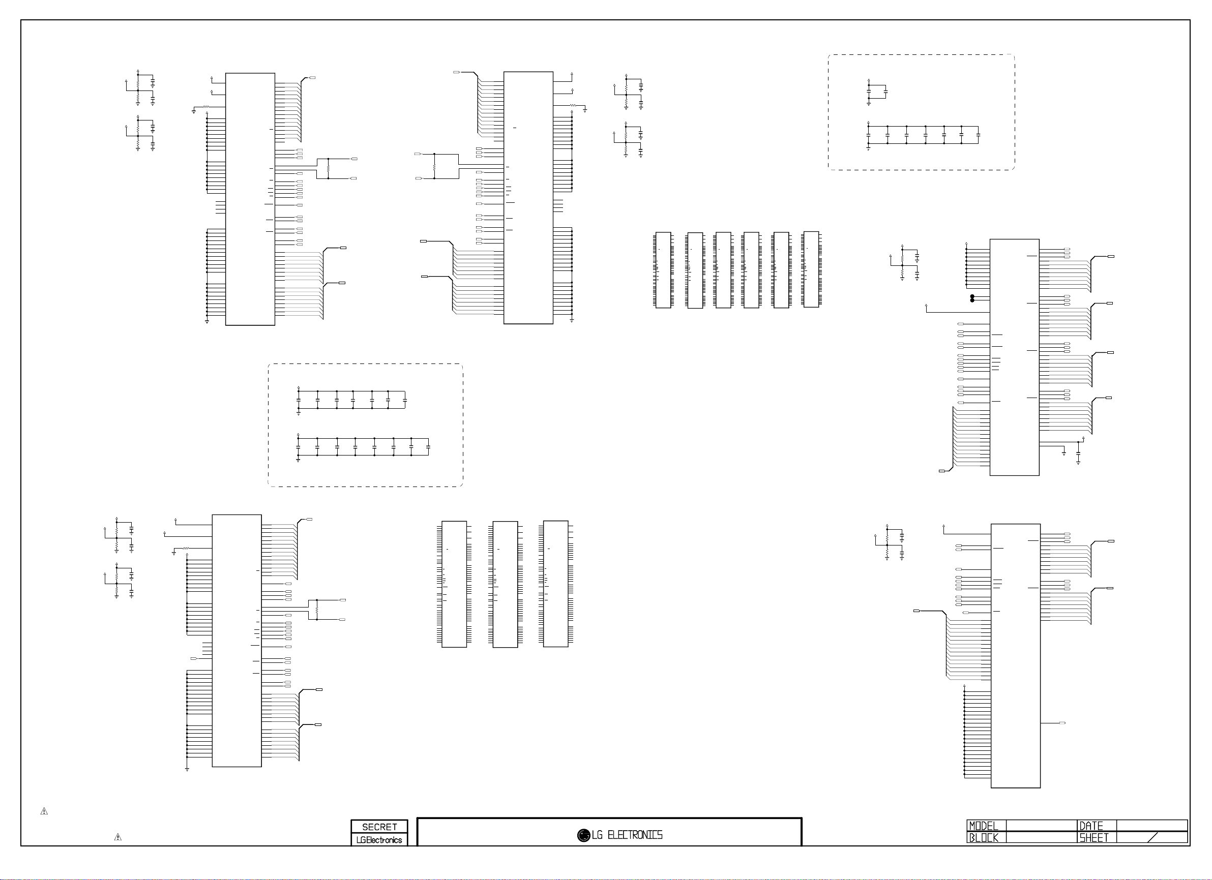
SCHEMATIC CIRCUIT DIAGRAM ..............................................................
Only for training and service purposes
- 2 -
LGE Internal Use OnlyCopyright © LG Electronics. Inc. All rights reserved.
SAFETY PRECAUTIONS
IMPORTANT SAFETY NOTICE
Many electrical and mechanical parts in this chassis have special safety-related characteristics. These parts are identified by in the
Schematic Diagram and Exploded View.
It is essential that these special safety parts should be replaced with the same components as recommended in this manual to prevent
Shock, Fire, or other Hazards.
Do not modify the original design without permission of manufacturer.
General Guidance
An isolation Transformer should always be used during the
servicing of a receiver whose chassis is not isolated from the AC
power line. Use a transformer of adequate power rating as this
protects the technician from accidents resulting in personal injury
from electrical shocks.
It will also protect the receiver and it's components from being
damaged by accidental shorts of th e cir cuitry that may be
inadvertently introduced during the service operation.
If any fuse (or Fusible Resistor) in this TV receiver is blown,
replace it with the specified.
When replacing a high wattage resistor (Oxide Metal Film Resistor,
over 1 W), keep the resistor 10 mm away from PCB.
Keep wires away from high voltage or high temperature parts.
Before returning the receiver to the customer,
always perform an AC leakage current check on the exposed
metallic parts of the cabinet, such as antennas, terminals, etc., to
be sure the set is safe to operate without damage of electrical
shock.
Leakage Current Cold Check(Antenna Cold Check)
With the instrument AC plug removed from AC source, connect an
electrical jumper across the two AC plug prongs. Place the AC
switch in the on position, connect one lead of ohm-meter to the AC
plug prongs tied together and touch other ohm-meter lead in turn to
each exposed metallic parts such as antenna terminals, phone
jacks, etc.
If the exposed metallic part has a return path to the chassis, the
measured resistance should be between 1 MΩ and 5.2 MΩ.
When the exposed metal has no return path to the chassis the
reading must be infinite.
An other abnormality exists that must be corrected before the
receiver is returned to the customer.
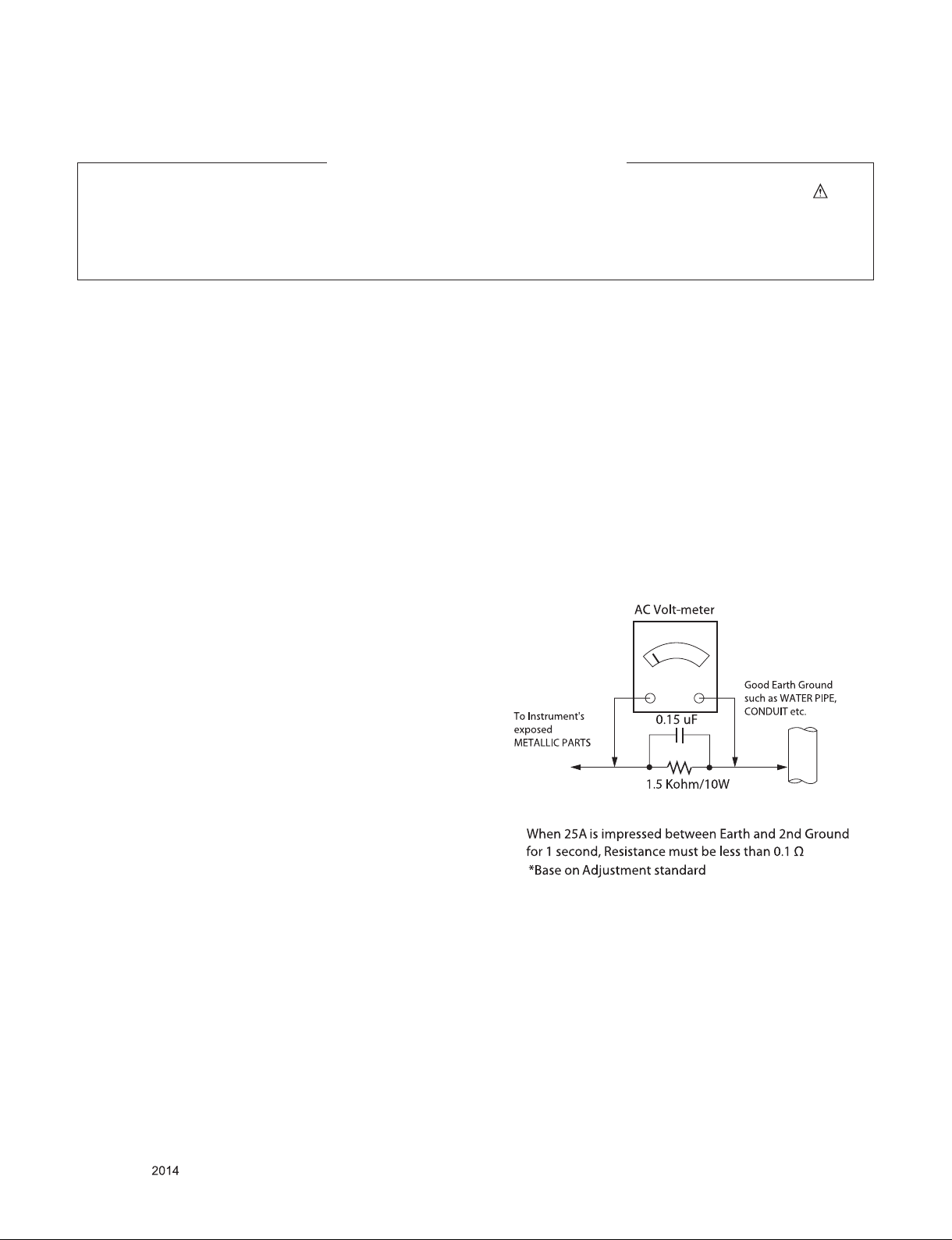
Leakage Current Hot Check (See below Figure)
Plug the AC cord directly into the AC outlet.
Do not use a line Isolation Transformer during this check.
Connect 1.5 K / 10 watt resistor in parallel with a 0.15 uF capacitor
between a known good earth ground (Water Pipe, Conduit, etc.)
and the exposed metallic parts.
Measure the AC voltage across the resistor using AC voltmeter
with 1000 ohms/volt or more sensitivity.
Reverse plug the AC cord into the AC outlet and repeat AC voltage
measurements for each exp ose d metallic par t. Any voltage
measured must not exceed 0.75 volt RMS which is corresponds to
0.5 mA.
In case any measurement is out of the limits specified, there is
possibility of shock hazard and the set must be checked and
repaired before it is returned to the customer.
Leakage Current Hot Check circuit
Only for training and service purposes
- 3 -
LGE Internal Use OnlyCopyright © LG Electronics. Inc. All rights reserved.

SERVICING PRECAUTIONS
CAUTION: Before servicing receivers covered by this service
manual and its supplements and addenda, read and follow the
SAFETY PRECAUTIONS on page 3 of this publication.
NOTE: If unforeseen circumstances create conict between the
following servicing precautions and any of the safety precautions
on page 3 of this publication, always follow the safety precautions.
Remember: Safety First.
General Servicing Precautions
1. Always unplug the receiver AC power cord from the AC power
source before;
a. Removing or reinstalling any component, circuit board mod-
ule or any other receiver assembly.
b. Disconnecting or reconnecting any receiver electrical plug or
other electrical connection.
c. Connecting a test substitute in parallel with an electrolytic
capacitor in the receiver.
CAUTION: A wrong part substitution or incorrect polarity
installation of electrolytic capacitors may result in an explosion hazard.
2. Test high voltage only by measuring it with an appropriate
high voltage meter or other voltage measuring device (DVM,
FETVOM, etc) equipped with a suitable high voltage probe.
Do not test high voltage by "drawing an arc".
3. Do not spray chemicals on or near this receiver or any of its
assemblies.
4. Unless specied otherwise in this service manual, clean
electrical contacts only by applying the following mixture to the
contacts with a pipe cleaner, cotton-tipped stick or comparable
non-abrasive applicator; 10 % (by volume) Acetone and 90 %
(by volume) isopropyl alcohol (90 % - 99 % strength)
CAUTION: This is a ammable mixture.
Unless specied otherwise in this service manual, lubrication of
contacts in not required.
5. Do not defeat any plug/socket B+ voltage interlocks with which
receivers covered by this service manual might be equipped.
6. Do not apply AC power to this instrument and/or any of its
electrical assemblies unless all solid-state device heat sinks are
correctly installed.
7. Always connect the test receiver ground lead to the receiver
chassis ground before connecting the test receiver positive
lead.
Always remove the test receiver ground lead last.
8. Use with this receiver only the test xtures specied in this
service manual.
CAUTION: Do not connect the test xture ground strap to any
heat sink in this receiver.
Electrostatically Sensitive (ES) Devices
Some semiconductor (solid-state) devices can be damaged easily by static electricity. Such components commonly are called
Electrostatically Sensitive (ES) Devices. Examples of typical ES
devices are integrated circuits and some eld-effect transistors
and semiconductor “chip” components. The following techniques
should be used to help reduce the incidence of component damage caused by static by static electricity.
1. Immediately before handling any semiconductor component or
semiconductor-equipped assembly, drain off any electrostatic
charge on your body by touching a known earth ground. Alternatively, obtain and wear a commercially available discharging
wrist strap device, which should be removed to prevent potential shock reasons prior to applying power to the unit under test.
2. After removing an electrical assembly equipped with ES
devices, place the assembly on a conductive surface such as
aluminum foil, to prevent electrostatic charge buildup or exposure of the assembly.
3. Use only a grounded-tip soldering iron to solder or unsolder ES
devices.
4. Use only an anti-static type solder removal device. Some solder
removal devices not classied as “anti-static” can generate
electrical charges sufcient to damage ES devices.
5. Do not use freon-propelled chemicals. These can generate
electrical charges sufcient to damage ES devices.
6. Do not remove a replacement ES device from its protective
package until immediately before you are ready to install it.
(Most replacement ES devices are packaged with leads electrically shorted together by conductive foam, aluminum foil or
comparable conductive material).
7. Immediately before removing the protective material from the
leads of a replacement ES device, touch the protective material
to the chassis or circuit assembly into which the device will be
installed.
CAUTION: Be sure no power is applied to the chassis or circuit,
and observe all other safety precautions.
8. Minimize bodily motions when handling unpackaged replacement ES devices. (Otherwise harmless motion such as the
brushing together of your clothes fabric or the lifting of your
foot from a carpeted oor can generate static electricity sufcient to damage an ES device.)
General Soldering Guidelines
1. Use a grounded-tip, low-wattage soldering iron and appropriate
tip size and shape that will maintain tip temperature within the
range or 500 °F to 600 °F.
2. Use an appropriate gauge of RMA resin-core solder composed
of 60 parts tin/40 parts lead.
3. Keep the soldering iron tip clean and well tinned.
4. Thoroughly clean the surfaces to be soldered. Use a mall wirebristle (0.5 inch, or 1.25 cm) brush with a metal handle.
Do not use freon-propelled spray-on cleaners.
5. Use the following unsoldering technique
a. Allow the soldering iron tip to reach normal temperature.
(500 °F to 600 °F)
b. Heat the component lead until the solder melts.
c. Quickly draw the melted solder with an anti-static, suction-
type solder removal device or with solder braid.
CAUTION: Work quickly to avoid overheating the circuit
board printed foil.
6. Use the following soldering technique.
a. Allow the soldering iron tip to reach a normal temperature
(500 °F to 600 °F)
b. First, hold the soldering iron tip and solder the strand against
the component lead until the solder melts.
c. Quickly move the soldering iron tip to the junction of the
component lead and the printed circuit foil, and hold it there
only until the solder ows onto and around both the component lead and the foil.
CAUTION: Work quickly to avoid overheating the circuit
board printed foil.
d. Closely inspect the solder area and remove any excess or
splashed solder with a small wire-bristle brush.
Only for training and service purposes
- 4 -
LGE Internal Use OnlyCopyright © LG Electronics. Inc. All rights reserved.

IC Remove/Replacement
Some chassis circuit boards have slotted holes (oblong) through
which the IC leads are inserted and then bent at against the circuit foil. When holes are the slotted type, the following technique
should be used to remove and replace the IC. When working with
boards using the familiar round hole, use the standard technique
as outlined in paragraphs 5 and 6 above.
Removal
1. Desolder and straighten each IC lead in one operation by
gently prying up on the lead with the soldering iron tip as the
solder melts.
2. Draw away the melted solder with an anti-static suction-type
solder removal device (or with solder braid) before removing
the IC.
Replacement
1. Carefully insert the replacement IC in the circuit board.
2. Carefully bend each IC lead against the circuit foil pad and
solder it.
3. Clean the soldered areas with a small wire-bristle brush.
(It is not necessary to reapply acrylic coating to the areas).
"Small-Signal" Discrete Transistor
Removal/Replacement
1. Remove the defective transistor by clipping its leads as close
as possible to the component body.
2. Bend into a "U" shape the end of each of three leads remaining
on the circuit board.
3. Bend into a "U" shape the replacement transistor leads.
4. Connect the replacement transistor leads to the corresponding
leads extending from the circuit board and crimp the "U" with
long nose pliers to insure metal to metal contact then solder
each connection.
Power Output, Transistor Device
Removal/Replacement
1. Heat and remove all solder from around the transistor leads.
2. Remove the heat sink mounting screw (if so equipped).
3. Carefully remove the transistor from the heat sink of the circuit
board.
4. Insert new transistor in the circuit board.
5. Solder each transistor lead, and clip off excess lead.
6. Replace heat sink.
Diode Removal/Replacement
1. Remove defective diode by clipping its leads as close as possible to diode body.
2. Bend the two remaining leads perpendicular y to the circuit
board.
3. Observing diode polarity, wrap each lead of the new diode
around the corresponding lead on the circuit board.
4. Securely crimp each connection and solder it.
5. Inspect (on the circuit board copper side) the solder joints of
the two "original" leads. If they are not shiny, reheat them and if
necessary, apply additional solder.
3. Solder the connections.
CAUTION: Maintain original spacing between the replaced
component and adjacent components and the circuit board to
prevent excessive component temperatures.
Circuit Board Foil Repair
Excessive heat applied to the copper foil of any printed circuit
board will weaken the adhesive that bonds the foil to the circuit
board causing the foil to separate from or "lift-off" the board. The
following guidelines and procedures should be followed whenever
this condition is encountered.
At IC Connections
To repair a defective copper pattern at IC connections use the
following procedure to install a jumper wire on the copper pattern
side of the circuit board. (Use this technique only on IC connections).
1. Carefully remove the damaged copper pattern with a sharp
knife. (Remove only as much copper as absolutely necessary).
2. carefully scratch away the solder resist and acrylic coating (if
used) from the end of the remaining copper pattern.
3. Bend a small "U" in one end of a small gauge jumper wire and
carefully crimp it around the IC pin. Solder the IC connection.
4. Route the jumper wire along the path of the out-away copper
pattern and let it overlap the previously scraped end of the
good copper pattern. Solder the overlapped area and clip off
any excess jumper wire.
At Other Connections
Use the following technique to repair the defective copper pattern
at connections other than IC Pins. This technique involves the
installation of a jumper wire on the component side of the circuit
board.
1. Remove the defective copper pattern with a sharp knife.
Remove at least 1/4 inch of copper, to ensure that a hazardous
condition will not exist if the jumper wire opens.
2. Trace along the copper pattern from both sides of the pattern
break and locate the nearest component that is directly connected to the affected copper pattern.
3. Connect insulated 20-gauge jumper wire from the lead of the
nearest component on one side of the pattern break to the lead
of the nearest component on the other side.
Carefully crimp and solder the connections.
CAUTION: Be sure the insulated jumper wire is dressed so the
it does not touch components or sharp edges.
Fuse and Conventional Resistor
Removal/Replacement
1. Clip each fuse or resistor lead at top of the circuit board hollow
stake.
2. Securely crimp the leads of replacement component around
notch at stake top.
Only for training and service purposes
- 5 -
LGE Internal Use OnlyCopyright © LG Electronics. Inc. All rights reserved.
SPECIFICATION
NOTE : Specifications and others are subject to change without notice for improvement
.
1. Application range
This specification is applied to the LED TV used LD46B
chassis.
2. Requirement for Test
Each part is tested as below without special appointment.
1) Temperature: 25 °C ± 5 °C(77 °F ± 9 °F), CST: 40 °C ± 5 °C
2) Relative Humidity: 65 % ± 10 %
3) Power Voltage
: Standard input voltage (AC 100-240 V~, 50/60 Hz)
* Standard Voltage of each products is marked by models.
4) Specification and performance of each parts are followed
ea ch drawing and s pe cificatio n b y p art number in
accordance with BOM.
5) The receiver must be operated for about 20 minutes prior to
the adjustment.
3. Test method
1) Performance: LGE TV test method followed
2) Demanded other specification
- Safety : CE, IEC, CU specification
- EMC : CE, IEC, CU
4. Model General Specification
No. Item Specication Remarks
1 Market EU(PAL Market-37Countries) DTV & Analog (Total 37 countries)
DTV (MPEG2/4, DVB-T) : 29 countries
Germany, Netherland, Switzerland, Hungary, Austria, Slovenia, Bulgaria, France, Spain, Italy, Belgium, Luxemburg,
Greece, Czech, Croatia, Turkey, Moroco, Ireland, Latvia,
Estonia, Lithuania, Poland, Portugal, Romania, Albania,
Bosnia, Serbia, Slovakia, Beralus
DTV (MPEG2/4, DVB-T2): 8 countries
UK(Ireland), Sweden, Denmark, Finland, Norway, Ukraine,
Kazakhstan, Russia
DTV (MPEG2/4, DVB-C): 37 countries
Germany, Netherland, Switzerland, Hungary, Austria,
Slovenia, Bulgaria, France, Spain, Italy, Belgium, Russia,
Luxemburg, Greece, Czech, Croatia, Turkey, Moroco, Ireland, Latvia, Estonia, Lithuania, Poland, Portugal, Romania,
Albania, Bosnia, Serbia, Slovakia, Beralus, UK, Sweden,
Denmark, Finland, Norway, Ukraine, Kazakhstan
DTV (MPEG2/4,DVB-S): 30 countries
Germany, Netherland, Switzerland, Hungary, Austria,
Slovenia, Bulgaria, France, Spain, Italy, Belgium, Russia,
Luxemburg, Greece, Czech, Croatia, Turkey, Moroco, Ireland, Latvia, Estonia, Lithuania, Poland, Portugal, Romania,
Albania, Bosnia, Serbia, Slovakia, Beralus
Supported satellite : 22 satellites
HISPASAT 1C/1D, ATLANTIC BIRD 2, NILESAT 101/102,
ATLANTIC BIRD 3, AMOS 2/3, THOR 5/6, IRIUS 4,
EUTELSAT-W3A, EUROBIRD 9A, EUTELSAT-W2A,
HOTBIRD 6/8/9, EUTELSAT-SESAT, ASTRA 1L/H/M/
KR, ASTRA 3A/3B, BADR 4/6, ASTRA 2D, EUROBIRD 3,
EUTELSAT-W7, HELLASSAT 2, EXPRESS AM1, TURKSAT 2A/3A, INTERSAT10
Only for training and service purposes
- 6 -
LGE Internal Use OnlyCopyright © LG Electronics. Inc. All rights reserved.
No. Item Specication Remarks
2 Broadcasting system
3 Program coverage
4 Receiving system
1) PAL-B/G
2) PAL-D/K
3) PAL-I
4) SECAM-L/L', D/K , B/G, I
5) DVB-T
6) DVB-C
7) DVB-T2
8) DVB-S/S2
1 ) Digital TV
- VHF, UHF
- C-Band,Ku-Band
2) Analogue TV
- VHF : E2 to E12
- UHF : E21 to E69
- CATV : S1 to S20
- HYPER : S21 to S47
Analog : Upper Heterodyne
Digital : COFDM, QAM
MODEL NAME
EU/CIS : T2/C/S2 - FHD “V”, HD “U”
T/C - FHD “0”, HD “B”
JA : T2/C/S2 – FHD “V”
T/C Model : 7) DVB-T2, 8) DVB-S/S2, not support.
C-Band*,Ku-Band* : Only T2/C/S2 Model.
► DVB-T
- Guard Interval(Bitrate_Mbit/s)
1/4, 1/8, 1/16, 1/32
- Modulation : Code Rate
QPSK : 1/2, 2/3, 3/4, 5/6, 7/8
16-QAM : 1/2, 2/3, 3/4, 5/6, 7/8
64-QAM : 1/2, 2/3, 3/4, 5/6, 7/8
► DVB-T2 (Model : *L*V*-Z* (T2 only Model))
- Guard Interval(Bitrate_Mbit/s)
1/4, 1/8, 1/16, 1/32, 1/128, 19/128, 19/256,
- Modulation : Code Rate
QPSK : 1/2, 2/5, 2/3, 3/4, 5/6
16-QAM : 1/2, 2/5, 2/3, 3/4, 5/6
64-QAM : 1/2, 2/5, 2/3, 3/4, 5/6
256-QAM: 1/2, 2/5, 2/3, 3/4, 5/6
► DVB-C
- Symbolrate : 4.0Msymbols/s to 7.2Msymbols/s
- Modulation : 16QAM, 64-QAM, 128-QAM and 256-QAM
► DVB-S/S2
- symbolrate
DVB-S2 (8PSK / QPSK) : 2 ~ 45Msymbol/s
DVB-S (QPSK) : 2 ~ 45Msymbol/s
- viterbi
DVB-S mode : 1/2, 2/3, 3/4, 5/6, 7/8
DVB-S2 mode : 1/2, 2/3, 3/4, 3/5, 4/5, 5/6, 8/9, 9/10
5 Scart (1EA) PAL, SECAM
6 Video Input RCA(1EA) PAL, SECAM, NTSC4.43
7 Head phone out
8 Component Input (1EA)
9 HDMI Input (2EA)
10 Audio Input (3EA)
11 SDPIF out (1EA) SPDIF out
12 USB (3EA) EMF, DivX HD, For SVC (download) JPEG, MP3, DivX HD
13 Ethernet Connect(1EA) Ethernet Connect
Antenna, AV1, AV2, Component, HDMI1,
HDMI2, HDMI3, USB1, USB2, USB3
Y/Cb/Cr
Y/Pb/Pr
HDMI1-DTV
HDMI2-DTV
HDMI3-DTV
DVI Audio
Component/AV2
AV1
Scart 1 Jack is Full scart and support ATV/DTV-OUT
(not support DTV Auto AV)
4 System : PAL, SECAM, NTSC4.43, PAL60
Hybrid Type
Hybrid Type
HDMI1: PC support(HDMI version 1.3)
Support HDCP
L/R Input.
Only for training and service purposes
- 7 -
LGE Internal Use OnlyCopyright © LG Electronics. Inc. All rights reserved.
5. Component Video Input (Y, Pb, Pr)
No. Resolution H-freq(kHz) V-freq(Hz) Pixel clock
1. 720×480 15.73 60.00 SDTV, DVD 480i
2. 720×480 15.63 59.94 SDTV, DVD 480i
3. 720×480 31.47 59.94 480p
4. 720×480 31.50 60.00 480p
5. 720×576 15.625 50.00 SDTV, DVD 625 Line
6. 720×576 31.25 50.00 SDTV 576p
7. 1280×720 45.00 50.00 HDTV 720p
8. 1280×720 44.96 59.94 HDTV 720p
9. 1280×720 45.00 60.00 HDTV 720p
10. 1920×1080 31.25 50.00 HDTV 1080i
11. 1920×1080 33.75 60.00 HDTV 1080i
12. 1920×1080 33.72 59.94 HDTV 1080i
13. 1920×1080 56.250 50 HDTV 1080p
14. 1920×1080 67.5 60 HDTV 1080p
Only for training and service purposes
- 8 -
LGE Internal Use OnlyCopyright © LG Electronics. Inc. All rights reserved.
6. HDMI Input
6.1. DTV mode
No. Resolution H-freq(kHz) V-freq.(Hz) Pixel clock(MHz)
1 640*480 31.469 / 31.5 59.94/60 SDTV 480P
2 720*480 31.469 / 31.5 59.94 / 60 SDTV 480P
3 720*576 31.25 50 SDTV 576P
4 720*576 15.625 50 SDTV 576I
5 1280*720 37.500 50 HDTV 720P
6 1280*720 44.96 / 45 59.94 / 60 HDTV 720P
7 1920*1080 33.72 / 33.75 59.94 / 60 HDTV 1080I
8 1920*1080 28.125 50.00 HDTV 1080I
9 1920*1080 26.97 / 27 23.97 / 24 HDTV 1080P
10 1920*1080 28.125 25 HDTV 1080P
11 1920*1080 33.716 / 33.75 29.976 / 30.00 HDTV 1080P
12 1920*1080 56.250 50 HDTV 1080P
13 1920*1080 67.43 / 67.5 59.94 / 60 HDTV 1080P
6.2. PC mode
No. Resolution H-freq(kHz) V-freq.(Hz) Pixel clock(MHz) Remarks
1 640 x 350 @70Hz 31.468 70.09 EGA
2 720 x 400 @70Hz 31.469 70.08 DOS
3 640 x 480 @60Hz 31.469 59.94 VESA(VGA)
4 800 x 600 @60Hz 37.879 60.31 VESA(SVGA)
5 1024 x 768 @60Hz 48.363 60.00 VESA(XGA)
6 1152 x 864 @60Hz 54.348 60.053 VESA
7 1280 x 1024 @60Hz 63.981 60.020 VESA(SXGA)
8 1360 x 768 @60Hz 47.712 60.015 VESA(WXGA)
9 1920 x 1080 @60Hz 67.5 60.00 WUXGA(Reduced Blanking)
Only for training and service purposes
- 9 -
LGE Internal Use OnlyCopyright © LG Electronics. Inc. All rights reserved.
ADJUSTMENT INSTRUCTION
1. Application Range
This specification sheet is applied to all of the LED TV with
LD46B chassis.
2. Designation
(1) Because this is not a hot chassis, it is not necessary to
use an isolation transformer. However, the use of isolation
transformer will help protect test instrument.
(2) Adjustment must be done in the correct order.
(3) The adjustment must be performed in the circumstance of
25 °C ± 5 °C of temperature and 65 % ± 10 % of relative
humidity if there is no specific designation.
(4) The input voltage of the receiver must keep AC 100-240
V~, 50/60 Hz.
(5) The receiver must be operated for about 5 minutes prior to
the adjustment when module is in the circumstance of over
15.
In case of keeping module is in the circumstance of 0 °C, it
should be placed in the circumstance of above 15 °C for 2
hours.
In case of keeping module is in the circumstance of below
-20 °C, it should be placed in the circumstance of above 15
°C for 3 hours.
[Caution]
When still image is displayed for a period of 20 minutes or
longer (Especially where W/B scale is strong. Digital pattern
13ch and/or Cross hatch pattern 09ch), there can some
afterimage in the black level area.
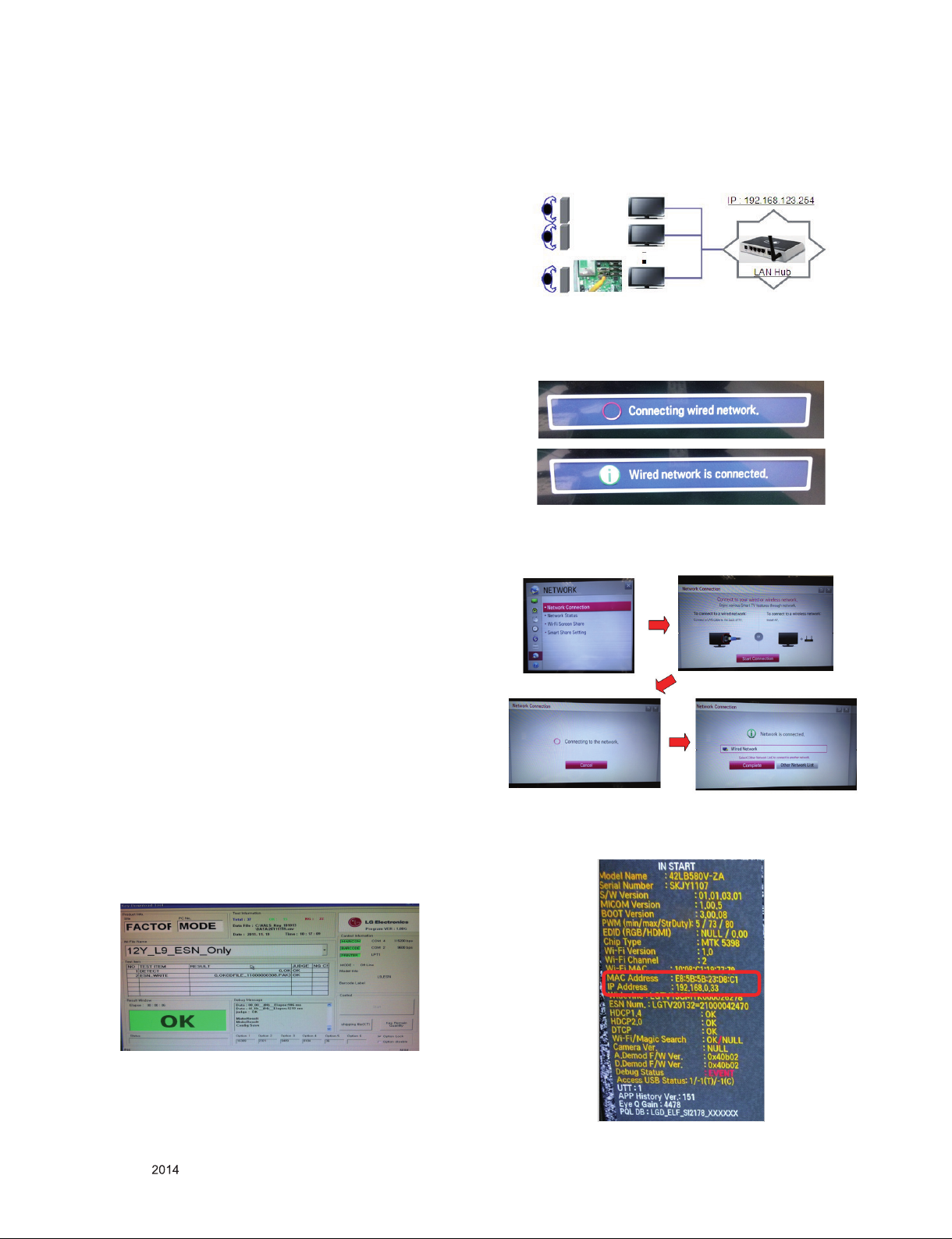
3.2. LAN Inspection
3.2.1. Equipment & Condition
▪ Each other connection to LAN Port of IP Hub and Jig
3.2.2. LAN inspection solution
▪ LAN Port connection with PCB
▪ Setting automatic IP
▪ If you want manual connection, enter Network connection at
MENU Mode of TV. Press Start connection key, then
Network will be connected.
3. Automatic Adjustment
3.1. MAC address D/L, CI+ key D/L, Widevine
key D/L, ESN D/L, HDCP14/20 D/L, DTCP
Connect: USB port
Communication Prot connection
▪ Com 1,2,3,4 and 115200(Baudrate)
Mode check: Online Only
▪ Check the test process: DETECT → MAC → CI → Widevine
→ ESN → HDCP14 → HDCP20 → DTCP
▪ Play: Press Enter key
▪ Result: Ready, Test, OK or NG
▪ Printer Out (MAC Address Label)
▪ Setting state confirmation
- If automatic setting is finished, you confirm IP and MAC
Address at ‘in start’ menu mode.
Only for training and service purposes
- 10 -
LGE Internal Use OnlyCopyright © LG Electronics. Inc. All rights reserved.
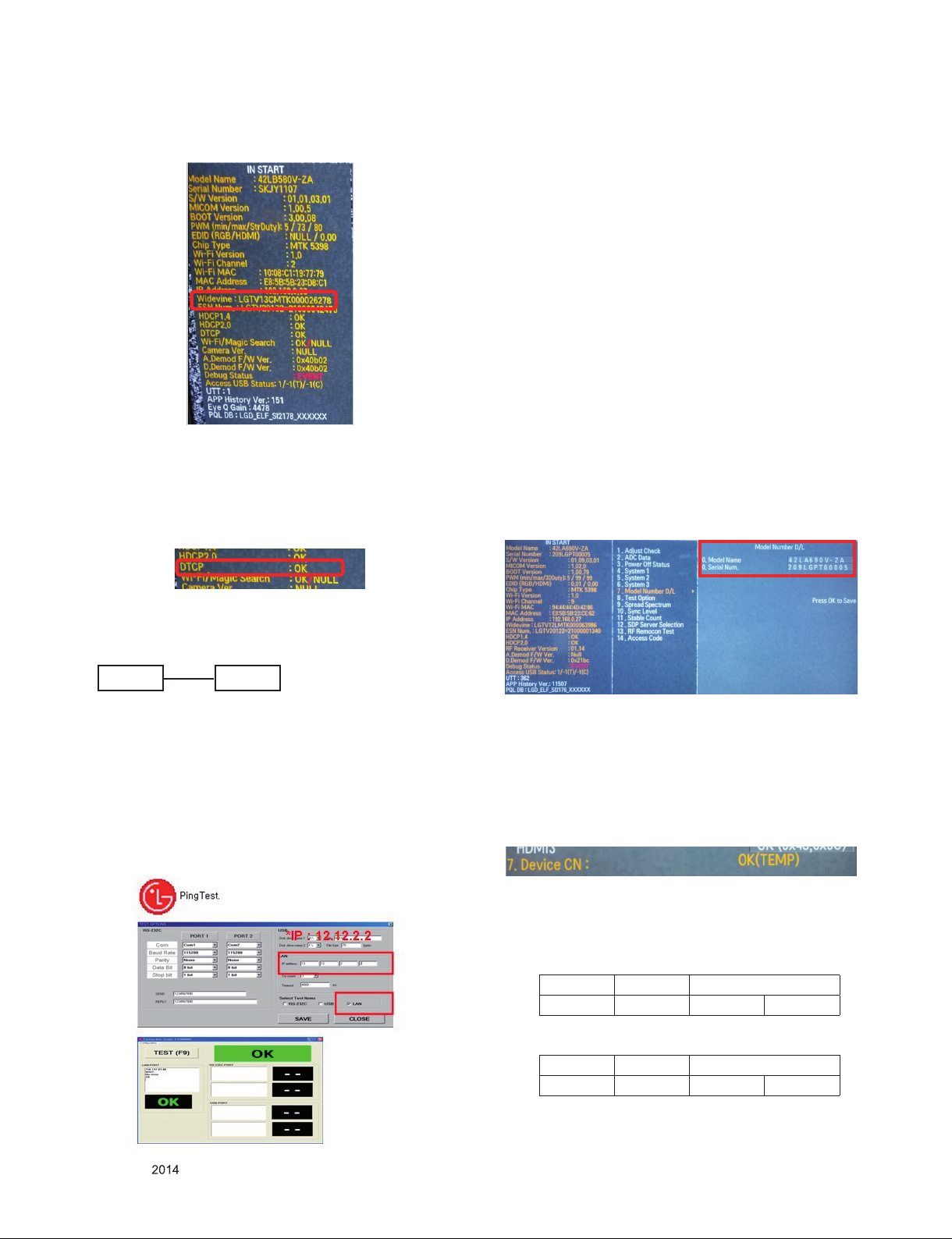
3.2.3. WIDEVINE key Inspection
- Confirm key input data at the "IN START" MENU Mode.
3.2.4. DTCP Inspection
- Confirm Key input Data at the “IN START” MENU Mode
- Below DTCP check on “IN START” MENU is enabled only
for Models which “DTCP key” tool option is “ON”.
- Only EU suffix models DTCP key option is on.
(ex.47LB580V-ZA.AEUWLHX)
3.4. Model name & Serial number Download
3.4.1. Model name & Serial number D/L
▪ Press "P-ONLY" key of service remote control.
(Baud rate : 115200 bps)
▪ Connect RS-232C Signal to USB Cable to USB.
▪ Write Serial number by use USB port.
▪ Must check the serial number at Instart menu.
3.4.2. Method & notice
(1) Serial number D/L is using of scan equipment.
(2) Setting of scan equipment operated by Manufacturing
Technology Group.
(3) Serial number D/L must be conformed when it is produced
in production line, because serial number D/L is mandatory
by D-book 4.0.
* Manual Download (Model Name and Serial Number)
If the TV set is downloaded by OTA or service man, sometimes
model name or serial number is initialized.(Not always)
There is impossible to download by bar code scan, so It
need Manual download.
1) Press the "Instart" key of Adjustment remote control.
2) Go to the menu "7.Model Number D/L" like below photo.
3) Input the Factory model name or Serial number like
photo.
3.3. LAN PORT INSPECTION(PING TEST)
Connect SET → LAN port == PC → LAN Port
SET PC
3.3.1. Equipment setting
(1) Play the LAN Port Test PROGRAM.
(2) Input IP set up for an inspection to Test Program.
*IP Number : 12.12.2.2
3.3.2. LAN PORT inspection(PING TEST)
(1) Play the LAN Port Test Program.
(2) Connect each other LAN Port Jack.
(3) Play Test (F9) button and confirm OK Message.
(4) Remove LAN cable.
4) Check the model name Instart menu. → Factory name
displayed. (ex 42LB580V-ZA)
5) Check the Diagnost ics.(DTV country only) → Buyer
model displayed. (ex 42LB580V-ZA)
3.5. CI+ Key checking method
Check whether the key was downloaded or not at ‘In Start’
menu. (Refer to below).
=> Check the Download to CI+ Key value in LGset.
3.5.1. Check the method of CI+ Key value
(1) Check the method on Instart menu
(2) Check the method of RS232C Command
1) Into the main ass’y mode(RS232: aa 00 00)
CMD 1 CMD 2 Data 0
A A 0 0
2) Check the key download for transmitted command
(RS232: ci 00 10)
CMD 1 CMD 2 Data 0
C I 1 0
3) Result value
- Normally status for download : OKx
- Abnormally status for download : NGx
Only for training and service purposes
- 11 -
LGE Internal Use OnlyCopyright © LG Electronics. Inc. All rights reserved.
3.5.2. Check the method of CI+ key value(RS232)
1) Into the main ass’y mode(RS232: aa 00 00)
CMD 1 CMD 2 Data 0
A A 0 0
2) Check the mothed of CI+ key by command
(RS232: ci 00 20)
CMD 1 CMD 2 Data 0
C I 2 0
3) Result value
i 01 OK 1d1852d21c1ed5dcx
CI+ Key Value
3.6. WIFI MAC ADDRESS CHECK
(1) Using RS232 Command
H-freq(kHz) V-freq.(Hz)
Transmission [A][I][][Set ID][][20][Cr] [O][K][X] or [NG]
(2) Check the menu on in-start
4. Manual Adjustment
* ADC adjustment is not needed because of OTP(Auto ADC
adjustment)
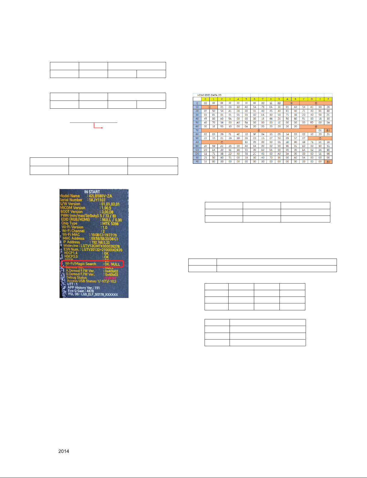
4.1. EDID DATA
4.1.1. 2D EDID(FHD)
▪ Reference
- HDMI1 ~ HDMI3
- In the data of EDID, bellows may be different by S/W or
Input mode.
ⓐ Product ID
HEX EDID Table DDC Function
0001 0100 Analog
0001 0100 Digital
ⓑ Serial No: Controlled on production line.
ⓒ Month, Year: Controlled on production line:
ex) Monthly : '01' → '01'
Year : '2014' → '18'
ⓓ Model Name(Hex): LGTV
Chassis MODEL NAME(HEX)
LD46S 00 00 00 FC 00 4C 47 20 54 56 0A 20 20 20 20 20 20 20
ⓔ Checksum(LG TV): Changeable by total EDID data.
ⓔ1 ⓔ2 ⓔ3
HDMI1 E7 1B X
HDMI2 E7 0B X
HDMI3 E7 FB X
ⓕ Vendor Specific(HDMI)
INPUT MODEL NAME(HEX)
HDMI1 67 03 0C 00 10 00 80 1E
HDMI2 67 03 0C 00 20 00 80 1E
HDMI3 67 03 0C 00 30 00 80 1E
Only for training and service purposes
- 12 -
LGE Internal Use OnlyCopyright © LG Electronics. Inc. All rights reserved.
4.1.2. 2D HD EDID(HD)
0 1 2 3 4 5 6 7 8 9 A B C D E F
00 00 FF FF FF FF FF FF 0 0 1E 6D a b
10 c 01 03 80 A0 5A 78 0A EE 91 A3 54 4C 99 26
20 0F 5 0 54 A1 08 00 31 40 45 40 61 40 71 40 01 01
30 01 01 01 01 01 01 66 21 50 B 0 51 00 1B 30 40 70
40 36 00 40 84 63 00 00 1E 64 19 00 40 41 00 26 30
50 18 88 36 00 40 84 63 00 00 18 00 00 00 FD 00 3A
60 3 E 1E 53 10 00 0A 20 20 20 20 20 20 d
70 d 01 e
80 02 03 25 F1 4E 10 1F 04 93 05 14 03 02 12 20 21
90 22 15 01 29 3D 06 C0 15 07 50 09 57 07 f
A0 f 01 1D 80 18 71 1C 16 20 58 2C 25
B0 00 40 84 63 00 00 9E 01 1D 00 BC 52 D0 1E 20 B8
C0 28 55 40 40 84 63 00 00 1E 8C 0A D0 8A 20 E0 2D
D0 10 10 3E 96 00 40 84 63 00 00 18 02 3A 80 18 71
E0 38 2D 40 58 2C 45 00 40 84 63 00 00 1E 00 0 0 00
F0 00 00 00 00 00 00 00 00 00 00 00 00 00 00 0 0 e
▪ Reference
- HDMI1 ~ HDMI2
- In the data of EDID, bellows may be different by S/W or
Input mode.
HEX EDID Table DDC Function
0001 0100 Analog
0001 0100 Digital
ⓐ Product ID
ⓑ Serial No: Controlled on production line.
ⓒ Month, Year: Controlled on production line:
ex) Monthly : '01' → '01'
Year : '2014' → '18'
ⓓ Model Name(Hex): LGTV
Chassis MODEL NAME(HEX)
LD33B 00 00 00 FC 00 4C 47 20 54 56 0A 20 20 20 20 20 20 20
4.2. White Balance Adjustment
4.2.1. Overview
▪ W/B adj. Objective & How-it-works
(1) Objective: To reduce each Panel's W/B deviation
(2) How-it-works : When R/G/B gain in the OSD is at 192, it
means the panel is at its Full Dynamic Range. In order to
prevent saturation of Full Dynamic range and data, one
of R/G/B is fixed at 192, and the other two is lowered to
find the desired value.
(3) Adjustment condition : normal temperature
1) Surrounding Temperature : 25 °C ± 5 °C
2) Surrounding Humidity : 20 % ~ 80 %
4.2.2. Equipment
(1) Color Analyzer: CA-210 (LED Module : CH 14)
(2) Adjustment Computer(During auto adj., RS-232C protocol
is needed)
(3) Adjustment Remote control
(4) Video Signal Generator MSPG-925F 720p/216-Gray
(Model: 217, Pattern: 49)
→ Only when internal pattern is not available
▪ Color Analyzer Matrix should be calibrated using CS-1000.
4.2.3. Equipment connection MAP
Co lor Anal yze r
Pro be
RS -232 C
Pattern Gen era to r
Sig nal Sou rce
* If TV internal pattern is used, not needed
RS- 232 C
Co mp ute r
RS- 232 C
ⓔ Checksum(LG TV): Changeable by total EDID data.
ⓕ Vendor Specific(HDMI)
INPUT MODEL NAME(HEX)
HDMI1 67 03 0C 00 10 00 80 1E
HDMI2 67 03 0C 00 20 00 80 1E
4.2.4. Adj. Command (Protocol)
<Command Format>
START 6E A 50 A LEN A 03 A CMD A 00 A VAL A CS STOP
- LEN: Number of Data Byte to be sent
- CMD: Command
- VAL: FOS Data value
- CS: Checksum of sent data
- A: Acknowledge
Ex) [Send: JA_00_DD] / [Ack: A_00_okDDX]
▪ RS-232C Command used during auto-adjustment.
RS-232C COMMAND
[CMD ID DATA]
wb 00 00 Begin White Balance adjustment
wb 00 10 Gain adjustment(internal white pattern)
wb 00 1f Gain adjustment completed
wb 00 20 Offset adjustment(internal white pattern)
wb 00 2f Offset adjustment completed
wb 00 ff
End White Balance adjustment
(internal pattern disappears )
Ex) wb 00 00 -> Begin white balance auto-adj.
wb 00 10 -> Gain adj.
ja 00 ff -> Adj. data
jb 00 c0
...
...
wb 00 1f → Gain adj. completed
*(wb 00 20(Start), wb 00 2f(end)) → Off-set adj.
wb 00 ff → End white balance auto-adj.
Explanation
Only for training and service purposes
- 13 -
LGE Internal Use OnlyCopyright © LG Electronics. Inc. All rights reserved.
▪ Adj. Map
Applied Model : LD46B Chassis ALL MODELS
Cool
Medium
Warm
Adj. item
R Gain j g 00 C0
G Gain j h 00 C0
B Gain j i 00 C0
R Cut
G Cut
B Cut
R Gain j a 00 C0
G Gain j b 00 C0
B Gain j c 00 C0
R Cut
G Cut
B Cut
R Gain j d 00 C0
G Gain j e 00 C0
B Gain j f 00 C0
R Cut
G Cut
Command
(lower caseASCII)
CMD1 CMD2 MIN MAX
Data Range
(Hex.)
4.2.5. Adj. method
(1) Auto adj. method
1) Set TV in adj. mode using P-Only key.
2) Zero calibrate probe then place it on the center of the
display.
3) Connect Cable.(RS-232C to USB)
4) Select mode in adj. Program and begin adj.
5) When adj. is complete (OK Sign), check adj. status pre
mode. (Cool, Medium, Warm)
6) Remove probe and RS-232C cable to complete adj.
▪ W/B Adj. must begin as start command “wb 00 00” , and
finish as end command “wb 00 ff”, and Adj. offset if need.
All models have to fix G gain(172).
(2) Manual adjustment. method
1) Set TV in Adj. mode using P-Only key.
2) Zero Calibrate the probe of Color Analyzer, then place it
on the center of LCD module within 10 cm of the surface.
3) Press ADJ key → EZ adjust using adj. R/C → 7. WhiteBalance then press the cursor to the right(key ►).
(When right key(►) is pressed 204 Gray internal pattern
will be displayed)
4) Adjust Cool modes
① Fix the one of R/G/B gain to 192 (default data) and
decrease the others.
(If G gain is adjusted over 172 and R and B gain less
than 192 , Adjust is O.K.)
② If G gain is less than 172, Increase G gain by up to
172, and then increase R gain and G gain same
amount of increasing G gain.
③ If R gain or B gain is over 255, Readjust G gain less
than 172, Conform to R gain is 255 or B gain is 255
5) Adjust two modes(Medium / Warm) Fix the one of R/G/B
gain to 192(default data) and decrease the others.
6) Adj. is completed, Exit adjust mode using “EXIT” key on
Remote control.
▪ If internal pattern is not available, use RF input. In EZ Adj.
menu 6.White Balance, you can select one of 2 Testpattern: ON, OFF. Default is inner (ON).
By selecting OFF, you can adjust using RF signal in 206
Gray pattern.
Default
(Decimal)
* CASE Cool
First adjust the coordinate far away from the target
value(x, y).
1) x, y > target
i) Decrease the R, G.
2) x, y < target
i) First decrease the B gain,
ii) Decrease the one of the others.
3) x > target, y < target
i) First decrease B, so make y a little more than the
target.
ii) Adjust x value by decreasing the R.
4) x < target, y > target
i) First decrease B, so make x a little more than the
target.
ii) Adjust x value by decreasing the G.
How to adjust
1. If G gain is adjusted over 172 and R gain and B
gain less than 192 , Adjust is O.K.
2. If G gain is less than 172 , increase G gain by up to
172, and then increase R gain and B gain same
amount of increasing G gain.
3. If R gain or B gain is over 255 , Readjust G gain
less than 172, Conform to R gain is 255 or B gain is
255
* CASE Medium / Warm
First adjust the coordinate far away from the target
value(x, y).
1) x, y > target
i) Decrease the R, G.
2) x, y < target
i) First decrease the B gain,
ii) Decrease the one of the others.
3) x > target, y < target
i) First decrease B, so make y a little more than the
target.
ii) Adjust x value by decreasing the R
4) x < target, y > target
i) First decrease B, so make x a little more than the
target.
ii) Adjust x value by decreasing the G
▪ Adjustment condition and cautionary items
1) Lighting condition in surrounding area
Surrounding lighting should be lower 10 lux. Try to
isolate adj. area into dark surrounding.
2) Probe location
: Color Analyzer(CA-210) probe should be within 10 cm
and perpendicular of the module surface (80° ~ 100°)
Only for training and service purposes
- 14 -
LGE Internal Use OnlyCopyright © LG Electronics. Inc. All rights reserved.
4.2.6. Reference (White balance Adj. coordinate and
color temperature)
▪ Luminance : 204 Gray
▪ Standard color coordinate and temperature using CS-1000
(over 26 inch)
Mode
Cool 0.271 0.270 13000 K 0.0000
Medium 0.286 0.289 9300 K 0.0000
Warm 0.313 0.329 6500 K 0.0000
▪ Standard color coordinate and temperature using CA-210(CH 14)
Mode
Cool 0.271 ± 0.002 0.270 ± 0.002 13000 K 0.0000
Medium 0.286 ± 0.002 0.289 ± 0.002 9300 K 0.0000
Warm 0.313 ± 0.002 0.329 ± 0.002 6500 K 0.0000
Coordinate
x y
Coordinate
x y
Temp ∆uv
Temp ∆uv
4.2.7. LED White balance table
- EDGE LED module change color coordinate because of
aging time.
- Apply under the color coordinate table, for compensated
aging time.
Model : (aging chamber) LB49/57/58_LGD/CMI
Aging
NC4.5
1 0-5 280 285 294 308 319 340
2 6-10 276 280 290 303 315 335
3 11-20 272 275 286 298 311 330
4 21-30 269 272 283 295 308 327
5 31-40 267 268 281 291 306 323
6 41-50 266 265 280 288 305 320
7 51-80 265 263 279 286 304 318
8 81-119 264 261 278 284 303 316
9 Over 120 264 260 278 283 303 315
* AUO, INX, Sharp, CSOT(In case of Cool speck is 13000 K)
Luminance
(cd/m^2)
time
(Min)
spec 271 270 286 289 313 329
target 275 276 289 299 317 335
Cool Medium Warm
x y x y x y
271 270 286 289 313 329
Cool med warm
x y x y x y
Min Typ Min Typ Min Typ
80 110 80 110 80 110
* Only March to December & Global
Model : (normal line) LB49/57/58_LGD/CMI
Aging
NC4.5
1 0-2 281 287 295 310 320 342
2 3-5 280 285 294 308 319 340
3 6-9 278 284 292 307 317 339
4 10-19 276 281 290 304 315 336
5 20-35 275 277 289 300 314 332
6 36-49 274 274 288 297 313 329
7 50-79 273 272 287 295 312 327
8 80-119 272 271 286 294 311 326
9 Over 120 271 270 285 293 310 325
* Only for the table for January & February
Model : (normal line) LB49/57/58_LGD/CMI
NC4.5
1 0-2 283 292 297 315 322 347
2 3-5 282 290 296 313 321 345
3 6-9 280 288 294 311 319 343
4 10-19 277 284 291 307 316 339
5 20-35 275 279 289 302 314 334
6 36-49 274 275 288 298 313 330
7 50-79 273 272 287 295 312 327
8 80-119 272 271 286 294 311 326
9 Over 120 271 270 285 293 310 325
time
(Min)
Aging
time
(Min)
Cool Medium Warm
x y x y x y
271 270 286 289 313 329
Cool Medium Warm
x y x y x y
271 270 286 289 313 329
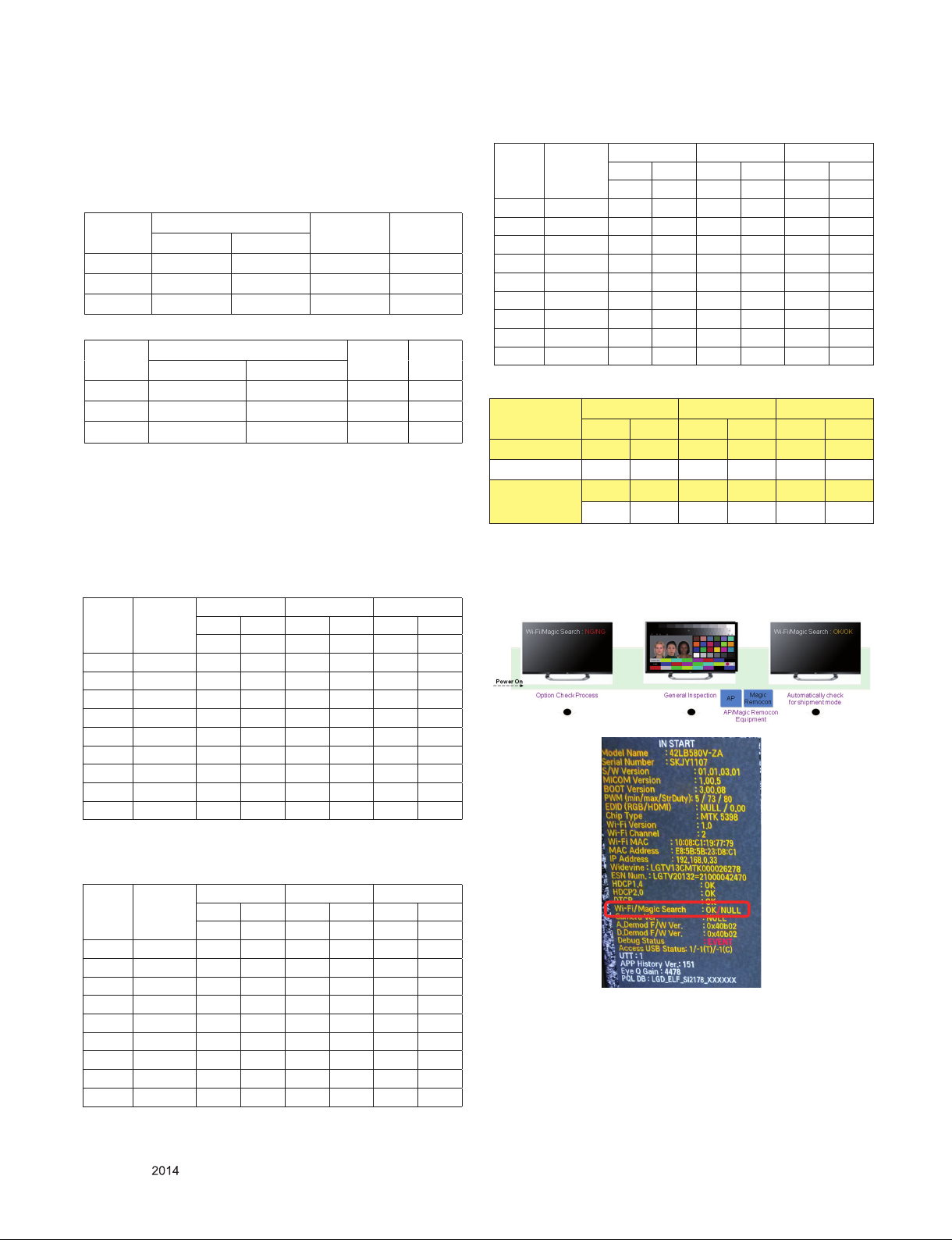
4.3. Magic Remote control test
- Re sults are automatically marked in In start OSD after
through the AP/Magic Remote control Equipment on the line
Only for training and service purposes
- 15 -
LGE Internal Use OnlyCopyright © LG Electronics. Inc. All rights reserved.
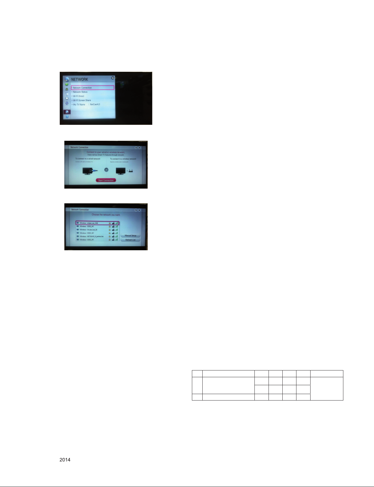
4.4. Wi-Fi Test
1) Turn on TV
2) Select Network Connection option in Network Menu.
5. Tool Option selection
▪ Method : Press "ADJ" key on the Adjustment remote control,
then select Tool option.
6. Ship-out mode check(In-stop)
▪ After final inspection, press "IN-STOP" key of the Adjustment
remote control and check that the unit goes to Stand-by
mode.
3) Select Start Connection button in Network Connection.
4) If the system finds any AP like blow PIC, it is working well.
4.5. LNB voltage and 22KHz tone check
(only for DVB-S/S2 model)
▪ Test method
(1) Set TV in Adj. mode using POWER ON.
(2) Connect cable between satellite ANT and test JIG.
(3) Press Yellow key(ETC+SWAP) in Adj Remote control to
make LNB on.
(4) Check LED light ‘ON’ at 18 V menu.
(5) Check LED light ‘ON’ at 22 KHz tone menu.
(6) Press Blue key(ETC+PIP INPUT) in Adj Remote control
to make LNB off.
(7) Check LED light ‘OFF’ at 18 V menu.
(8) Check LED light ‘OFF’ at 22 KHz tone menu.
7. GND and Internal Pressure check
7.1. Method
(1) GND & Internal Pressure auto-check preparation
- Check that Power cord is fully inserted to the SET.
(If loose, re-insert)
(2) Perform GND & Internal Pressure auto-check
- Unit fully inserted Power cord, Antenna cable and A/V
arrive to the auto-check process.
- Connect D-terminal to AV JACK TESTER
- Auto CONTROLLER(GWS103-4) ON
- Perform GND TEST
- If NG, Buzzer will sound to inform the operator.
- If OK, changeover to I/P check automatically.
(Remove CORD, A/V form AV JACK BOX.)
- Perform I/P test
- If NG, Buzzer will sound to inform the operator.
- If OK, Good lamp will lit up and the stopper will allow the
pallet to move on to next process.
7.2. Checkpoint
▪ TEST voltage
(1) DQA Test
- GND: AC 1.5 KV/min, Cut off current not exceed 100 mA
- SIGNAL: AC 3.0 KV/min, Cut off current not exceed 100
mA
(2) Mass Production Line Test
- GND: AC 1.5 KV/sec, Cut off current not exceed 100 mA
▪ TEST time: DQA 1 min, Mass Production Line 1 sec
▪ TEST POINT
- GND TEST = POWER CORD GND & SIGNAL CABLE
METAL GND
- Internal Pressure TEST = POWER CORD GND & LIVE &
NEUTRAL
▪ LEAKAGE CURRENT: At 0.5 mArms
▪ Test result
(1) After press LNB On key, ‘18 V LED’ and ‘22 KHz tone
LED’ should be ON.
(2) After press LNB OFF key, ‘18 V LED’ and ‘22 KHz tone
LED’ should be OFF.
4.6. Option selection per country
4.6.1. Overview
- Option selection is only done for models in Non-EU
4.6.2. Method
(1) Press ADJ key on the Adj. R/C, then select Country Group
Meun.
(2) Select Country Group Code 04 or Country Group EU
Only for training and service purposes
8. Audio
No. Item Min Typ Max Unit Remark
Audio practical max Out-
1.
put, L/R(Distortion=10%
max Output)
2. Speaker(8 Ω Impedance) 9 10 12 W
Measurement condition:
(1) RF input: Mono, 1 KHz sine wave signal, 100 % Modulation
(2) CVBS, Component: 1 KHz sine wave signal 0.5 Vrms
- 16 -
9 10 12 W
8.10 10.8 Vrms
LGE Internal Use OnlyCopyright © LG Electronics. Inc. All rights reserved.
EQ Off
AVL Off
Clear Voice Off

9. USB S/W Download(Service only)
(1) Put the USB Stick to the USB socket
(2) Automatically detecting update file in USB Stick
- If your downloaded program version in USB Stick is
Lower, it didn’t work.
But your downloaded version is Higher, USB data is
automatically detecting (Download Version High & Power
only mode, Set is automatically Download)
(3) Show the message “Do not unplug!”.
(4) Updating is starting.
(5) Updating completed, the TV will restart automatically.
(6) If your TV is turned on, check your updated version and
Tool option. (explain the Tool option, next stage)
* If downloading version is more high than your TV have,
TV can lost all channel data. In this case, you have to
channel recover. if all channel data is cleared, you didn’t
have a DTV/ATV test on production line.
* After downloading, have to adjust Tool Option again.
(1) Push "IN-START" key in service remote control.
(2) Select "Tool Option 1" and push "OK" key.
(3) Punch in the number. (Each model has their number)
Only for training and service purposes
- 17 -
LGE Internal Use OnlyCopyright © LG Electronics. Inc. All rights reserved.
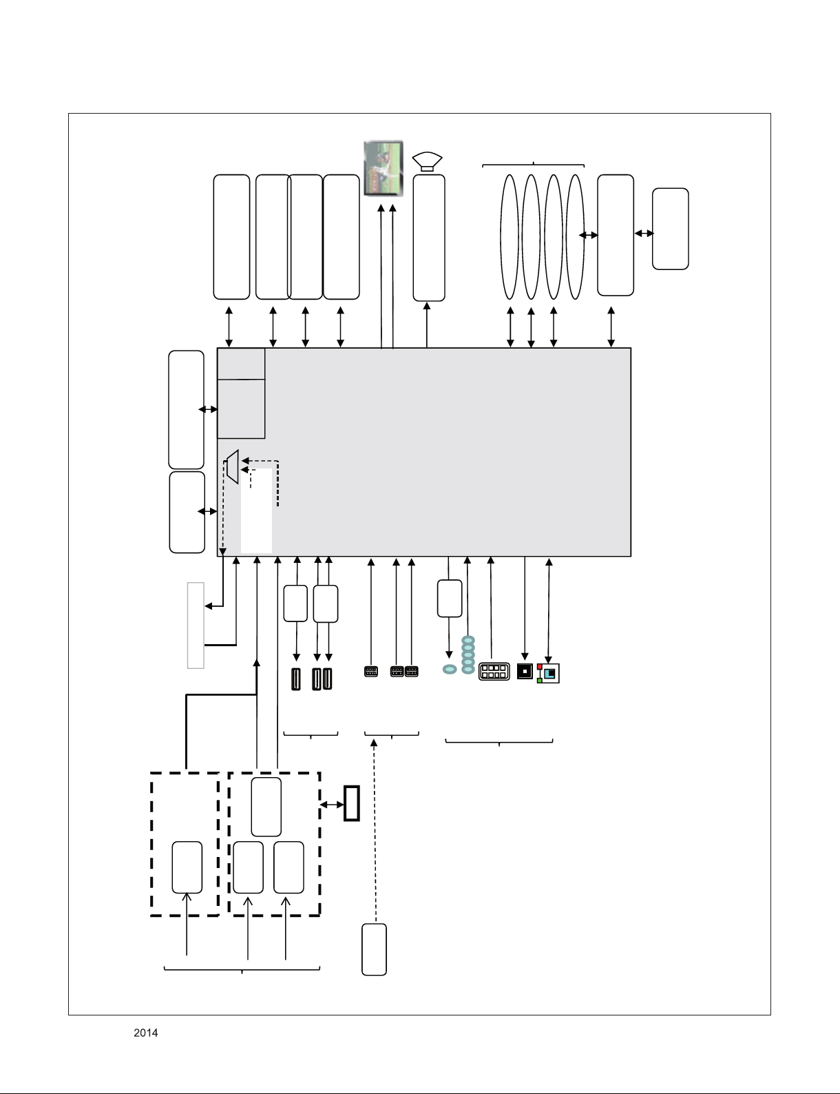
BLOCK DIAGRAM
SUB
ASSY
(4GB)
(256Kb)
(256MB X 1EA)
DDR3 1600 X 16
A B
(512MB X 2EA)
DDR3 1600 X 16
HDCP EEPROM
SYSTEM EEPROM
51P or 51P/41P or 30P
I2C 1
I2C 5
LVDS
(NTP7513)
Audio AMP
I2C 1
I2S Out
IR / NFC
Joystick KEY
IR
KEY
eMMC
(16Kb)
Eye-Q
WIFI
USB_WIFI
Sub Micom
(RENESAS R5F1000G)
I2C 3
X_TAL
32.768KHz
LGE 2122
X_TAL
27MHz
P_TS
Analog Demod
T/C Demod
P_TS
IF (+/-)
CI Slot
P_TS
USB
1A
OCP
1.5A
P_TS
OCP
MUX
HDMI
CVBS/YPbPr
CVBS/RGB
TI
AMP
ETHERNET
SPDIF OUT
(A)
TUNER
T/C Without ATV
Air/
Cable
Air/
REA
Only for training and service purposes
USB1
USB2
USB3
(HDD)
SID
Tuner : I2C 6
DEMOD
(T2/C/S2)
(A)
TUNER
Cable
R
(S2)
TUNER
T2/C/S2 Without ATV
DVB-S
(H)
HDMI1
HDMI2
E
DVB-S : I2C 4
SID
LNB
MHL
MHL 1A
SIL1292
MHL : I2C 4
H/P
HDMI3
E
SCART
AV/COMP
REA
- 18 -
LAN
OPTIC
R
LGE Internal Use OnlyCopyright © LG Electronics. Inc. All rights reserved.
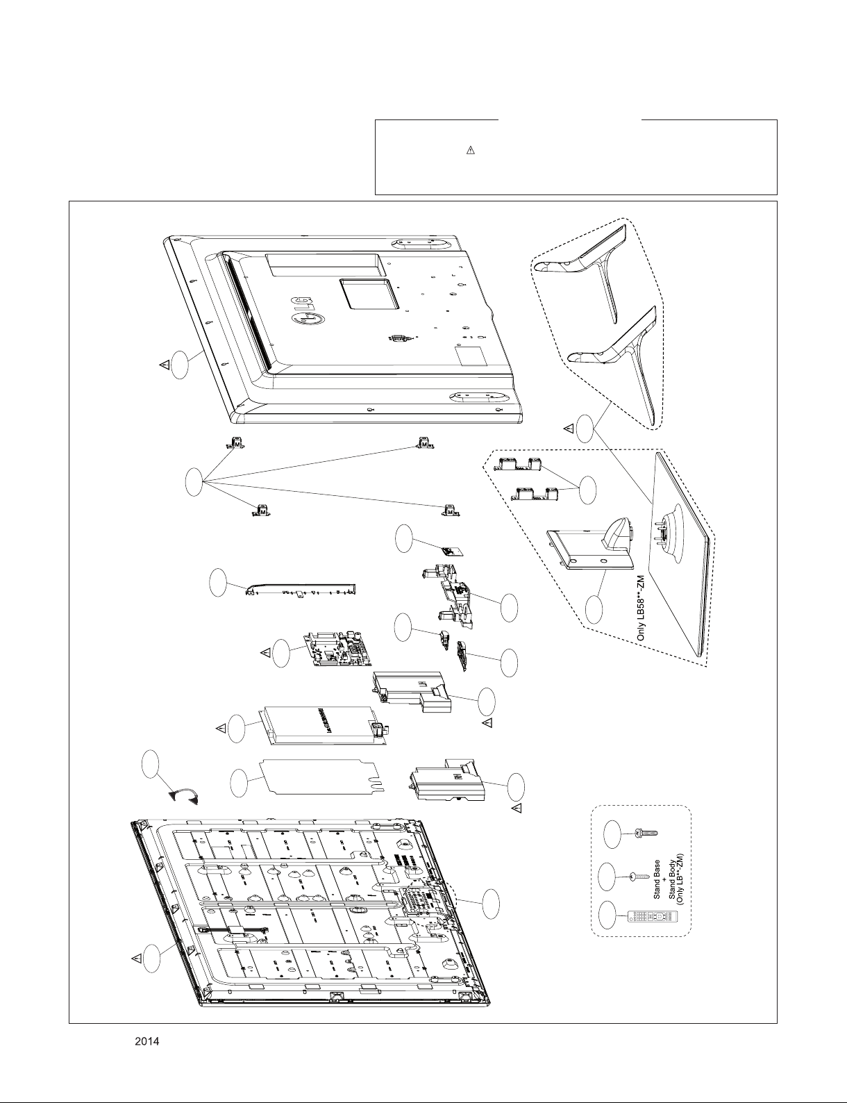
400
EXPLODED VIEW
IMPORTANT SAFETY NOTICE
Many electrical and mechanical parts in this chassis have special safety-related characteristics. These
parts are identified by in the Schematic Diagram and EXPLODED VIEW.
It is essenti al that these special safet y parts shoul d be replac ed with the same compo nents as
recommended in this manual to prevent X-RADIATION, Shock, Fire, or other Hazards.
Do not modify the original design without permission of manufacturer.
900
410
810
570
521
310
910
500
540
501
121
530
LV1
820
120
A10
Set + Stand
A9
200
Only for training and service purposes
- 19 -
200T
T-con board
(Option)
A2
LGE Internal Use OnlyCopyright © LG Electronics. Inc. All rights reserved.
WOL_CTL
Copyright © 2014 LG Electronics. Inc. All rights reserved.
Only for training and service purposes
LGE Internal Use Only
VDD3V3
+3.5V_ST
R500
10K
B
C500
4.7uF
10V
OPT
R502
R501
+3.5V_ST_WAKE
10K
1.8K
C
Q500
MMBT3904(NXP)
E
+3.3V_NORMAL
OPT
L503
BLM18PG121SN1D
OPT
L502
BLM18PG121SN1D
Q501
PMV48XP
S
G
C501
4.7uF
10V
L501
BLM18PG121SN1D
C503
10uF
OPT
C504
0.1uF
D
C502
0.1uF
16V
OPT
VDD3V3
C505
10uF
AVDD_33SB
C506
0.1uF
+3.5V_ST_WAKE
ZD500
IC105
+1.2V_MTK_CORE
3.3V_EMMC
L505
BLM18PG121SN1D
+1.2V_MTK_CORE
OPT
C513
10uF
POWER_ON/OFF1
C531
0.1uF
16V
OPT
C527
0.1uF
TP500
OPT
C535
0.1uF
LAN_JACK_POWER
TP501
VDD3V3
C510
0.1uF
16V
+1.2V_MTK_CORE
+1.2V_MTK_CORE
IC500
AP2121N-3.3TRE1
VIN
3
1
60mA
C507
C508
0.1uF
2.2uF
+3.5V_ST_WAKE
5V
OPT
C514
10uF
L504
BLM18PG121SN1D
VOUT
2
GND
C517
10uF
5600mA
C523
0.1uF
C518
10uF
AVDD_33SB
C512
1uF
10V
C532
C520
0.1uF
0.1uF
+1.2V_MTK_AVDD
+3.3V_NORMAL
DECAP FOR SOC (HIDDEN - UCC) DECAP FOR SOC Rework (BOTTOM)
+1.5V_DDR
C509
0.1uF
C511
0.1uF
+1.2V_MTK_CORE
+1.5V_DDR
OPT
C539
0.1uF
TP502
VDD3V3
OPT
C541
0.1uF
16V
TP503
LGE2122[A2_M13]
L11
VCCK_1
N12
VCCK_2
P12
VCCK_3
AG5
VCCK_4
AH5
VCCK_5
AJ5
VCCK_6
AK5
VCCK_7
AL5
VCCK_8
AM5
VCCK_9
AN5
VCCK_10
AK6
VCCK_11
AL6
VCCK_12
AM6
VCCK_13
AN6
VCCK_14
M11
VCCK_15
N11
VCCK_16
P11
VCCK_17
R11
VCCK_18
M12
VCCK_19
R12
VCCK_20
L13
VCCK_21
L14
VCCK_22
L15
VCCK_23
L17
VCCK_24
L18
VCCK_25
L19
VCCK_26
T11
VCCK_27
U11
VCCK_28
V11
VCCK_29
W11
VCCK_30
Y11
VCCK_31
AA11
VCCK_32
AB11
VCCK_33
AC11
VCCK_34
R23
VCCK_35
L12
VCCK_36
W12
VCCK_37
V23
VCCK_38
Y12
VCCK_39
AF6
VCCK_40
AG6
VCCK_41
AH6
VCCK_42
AJ6
VCCK_43
AE7
VCCK_44
AF7
VCCK_45
AG7
VCCK_46
AD8
VCCK_47
AE8
VCCK_48
AF8
VCCK_49
AE9
VCCK_50
AC10
VCCK_51
AD10
VCCK_52
AD11
VCCK_53
AE10
VCCK_54
AF9
VCCK_55
AG8
VCCK_56
AH7
VCCK_57
AJ7
VCCK_58
AK7
VCCK_59
AL7
VCCK_60
AM7
VCCK_61
AN7
VCCK_62
L16
VCCK_63
V12
VCCK_64
U12
VCCK_65
T12
VCCK_66
AD13
VCCK_67
AD17
VCCK_68
AD14
VCCK_69
AB12
VCCK_70
AA12
VCCK_71
AC12
VCCK_72
T9
VCC3IO_C
Y10
VCC3IO_B_1
AA10
VCC3IO_B_2
D22
VCC3IO_A_1
E22
VCC3IO_A_2
AC18
DVSS_1
AB21
DVSS_2
AB14
DVSS_3
N13
DVSS_4
P13
DVSS_5
R13
DVSS_6
T13
DVSS_7
U13
DVSS_8
V13
DVSS_9
W13
DVSS_10
Y13
DVSS_11
P18
DVSS_12
N14
DVSS_13
P14
DVSS_14
R14
DVSS_15
T14
DVSS_16
U14
DVSS_17
V14
DVSS_18
W14
DVSS_19
Y14
DVSS_20
R18
DVSS_21
N15
DVSS_22
P15
DVSS_23
DVSS_24
DVSS_25
DVSS_26
DVSS_27
DVSS_28
DVSS_29
DVSS_30
DVSS_31
DVSS_32
DVSS_33
DVSS_34
DVSS_35
DVSS_36
DVSS_37
DVSS_38
DVSS_39
DVSS_40
DVSS_41
DVSS_42
DVSS_43
DVSS_44
DVSS_45
DVSS_46
DVSS_47
DVSS_48
DVSS_49
DVSS_50
DVSS_51
DVSS_52
DVSS_53
DVSS_54
DVSS_55
DVSS_56
DVSS_57
DVSS_58
DVSS_59
DVSS_60
DVSS_61
DVSS_62
DVSS_63
DVSS_64
DVSS_65
DVSS_66
DVSS_67
DVSS_68
DVSS_69
DVSS_70
DVSS_71
DVSS_72
DVSS_73
DVSS_74
DVSS_75
DVSS_76
DVSS_77
DVSS_78
DVSS_79
DVSS_80
DVSS_81
DVSS_82
DVSS_83
DVSS_84
DVSS_85
DVSS_86
DVSS_87
DVSS_88
DVSS_89
DVSS_90
DVSS_91
DVSS_92
DVSS_93
DVSS_94
DVSS_95
DVSS_96
DVSS_97
DVSS_98
DVSS_99
DVSS_100
DVSS_101
DVSS_102
DVSS_103
DVSS_104
DVSS_105
DVSS_106
DVSS_107
DVSS_108
DVSS_109
DVSS_110
DVSS_111
DVSS_112
DVSS_113
DVSS_114
DVSS_115
DVSS_116
DVSS_117
DVSS_118
DVSS_119
DVSS_120
DVSS_121
DVSS_122
DVSS_123
DVSS_124
DVSS_125
DVSS_126
DVSS_127
R15
T15
U15
V15
W15
Y15
AA15
AB15
T18
R16
T16
U16
V16
W16
Y16
AA16
AB16
R17
T17
U17
V17
Y17
N16
V18
Y18
P16
V19
Y19
W17
AA17
AB17
N19
AC14
C13
K24
K25
L24
M17
M18
M19
P17
P19
N18
U20
V20
W20
Y20
AA20
R19
T19
M20
N20
U21
V21
W21
Y21
AA21
P20
R20
T20
U22
V22
W22
Y22
AA22
N21
P21
R21
T21
M22
N22
P22
R22
T22
M21
AC17
AA19
M13
M14
M15
AA13
AB13
AA14
AB19
D6
W19
U19
N17
L3
AB18
AA18
W18
U18
D16
AC13
M16
AC20
AC22
AD20
Y23
AA23
AB23
V24
W23
THE SYMBOL MARK OF THIS SCHEMETIC DIAGRAM INCORPORATES
SPECIAL FEATURES IMPORTANT FOR PROTECTION FROM X-RADIATION.
FIRE AND ELECTRICAL SHOCK HAZARDS, WHEN SERVICING IF IS
ESSENTIAL THAT ONLY MANUFACTURES SPECIFIED PARTS BE USED FOR
THE CRITICAL COMPONENTS IN THE SYMBOL MARK OF THE SCHEMETIC.
MID_MAIN_3
2011.12.09
10
A_RVREF1
Copyright © 2014 LG Electronics. Inc. All rights reserved.
Only for training and service purposes
LGE Internal Use Only
A_RVREF4
+1.5V_DDR
+1.5V_DDR
R706
1K
1%
R707
1K
1%
R708
1K
1%
R709
1K1%C716
C713
0.1uF
C714
0.1uF
C715
0.1uF
0.1uF
R710
A_RVREF4
A_RVREF1
+1.5V_DDR
M8
H1
1%
240
L8
B2
D9
G7
K2
K8
N1
N9
R1
R9
A1
A8
C1
C9
D2
E9
F1
H2
H9
J1
J9
L1
L9
A9
B3
E1
G8
J2
J8
M1
M9
P1
P9
T1
T9
B1
B9
D1
D8
E2
E8
F9
G1
G9
DDR_512MB_SS
IC701
K4B4G1646B-HCK0
VREFCA
VREFDQ
ZQ
VDD_1
VDD_2
VDD_3
VDD_4
VDD_5
VDD_6
VDD_7
VDD_8
VDD_9
VDDQ_1
VDDQ_2
VDDQ_3
VDDQ_4
VDDQ_5
VDDQ_6
VDDQ_7
VDDQ_8
VDDQ_9
NC_1
NC_2
NC_3
NC_4
VSS_1
VSS_2
VSS_3
VSS_4
VSS_5
VSS_6
VSS_7
VSS_8
VSS_9
VSS_10
VSS_11
VSS_12
VSSQ_1
VSSQ_2
VSSQ_3
VSSQ_4
VSSQ_5
VSSQ_6
VSSQ_7
VSSQ_8
VSSQ_9
A10/AP
A12/BC
RESET
DDR_512MB_SS
IC703
ARA[0-14]
ARA[0]
N3
A0
ARA[1]
P7
A1
ARA[2]
P3
A2
ARA[3]
N2
A3
ARA[4]
P8
A4
ARA[5]
P2
A5
ARA[6]
R8
A6
ARA[7]
R2
A7
ARA[8]
T8
A8
ARA[9]
R3
A9
ARA[10]
L7
ARA[11]
R7
A11
ARA[12]
N7
ARA[13]
T3
A13
ARA[14]
T7
A14
M7
A15
M2
BA0
BA1
BA2
CK
CK
CKE
CS
ODT
RAS
CAS
WE
DQSL
DQSL
DQSU
DQSU
DML
DMU
DQL0
DQL1
DQL2
DQL3
DQL4
DQL5
DQL6
DQL7
DQU0
DQU1
DQU2
DQU3
DQU4
DQU5
DQU6
DQU7
ARBA0
N8
ARBA1
M3
ARBA2
J7
K7
K9
ARCKE
L2
/ARCS
K1
ARODT
J3
/ARRAS
K3
/ARCAS
L3
/ARWE
T2
ARREST
F3
ARDQS0
G3
/ARDQS0
C7
ARDQS1
B7
/ARDQS1
E7
ARDQM0
D3
ARDQM1
ARDQ[0]
E3
ARDQ[1]
F7
ARDQ[2]
F2
ARDQ[3]
F8
ARDQ[4]
H3
ARDQ[5]
H8
ARDQ[6]
G2
ARDQ[7]
H7
ARDQ[8]
D7
ARDQ[9]
C3
ARDQ[10]
C8
ARDQ[11]
C2
ARDQ[12]
A7
ARDQ[13]
A2
ARDQ[14]
B8
ARDQ[15]
A3
ARCLK0
R712
100
5%
/ARCLK0
ARDQ[0-7]
ARDQ[8-15]
ARCLK1
/ARCLK1
ARDQ[16-23]
ARDQ[24-31]
ARA[0-14]
R714
100
5%
ARDQ[16]
ARDQ[17]
ARDQ[18]
ARDQ[19]
ARDQ[20]
ARDQ[21]
ARDQ[22]
ARDQ[23]
ARDQ[24]
ARDQ[25]
ARDQ[26]
ARDQ[27]
ARDQ[28]
ARDQ[29]
ARDQ[30]
ARDQ[31]
ARBA0
ARBA1
ARBA2
ARCKE
/ARCSX
ARODT
/ARRAS
/ARCAS
/ARWE
ARREST
ARDQS2
/ARDQS2
ARDQS3
/ARDQS3
ARDQM2
ARDQM3
ARA[0]
ARA[1]
ARA[2]
ARA[3]
ARA[4]
ARA[5]
ARA[6]
ARA[7]
ARA[8]
ARA[9]
ARA[10]
ARA[11]
ARA[12]
ARA[13]
ARA[14]
K4B4G1646B-HCK0
N3
A0
P7
A1
P3
A2
N2
A3
P8
A4
P2
A5
R8
A6
R2
A7
T8
A8
R3
A9
L7
A10/AP
R7
A11
N7
A12/BC
T3
A13
T7
A14
M7
A15
M2
BA0
N8
BA1
M3
BA2
J7
CK
K7
CK
K9
CKE
L2
CS
K1
ODT
J3
RAS
K3
CAS
L3
WE
T2
RESET
F3
DQSL
G3
DQSL
C7
DQSU
B7
DQSU
E7
DML
D3
DMU
E3
DQL0
F7
DQL1
F2
DQL2
F8
DQL3
H3
DQL4
H8
DQL5
G2
DQL6
H7
DQL7
D7
DQU0
C3
DQU1
C8
DQU2
C2
DQU3
A7
DQU4
A2
DQU5
B8
DQU6
A3
DQU7
+1.5V_DDR
C718
0.1uF
C720
0.1uF
C722
0.1uF
C726
0.1uF
C728
0.1uF
C703
10uF
1uF
10V
C701
+1.5V_DDR
C708
C717
0.1uF
C719
0.1uF
C750
0.1uF
C723
0.1uF
C725
0.1uF
C727
0.1uF
C706
10uF
1uF
10V
VREFCA
VREFDQ
VDD_1
VDD_2
VDD_3
VDD_4
VDD_5
VDD_6
VDD_7
VDD_8
VDD_9
VDDQ_1
VDDQ_2
VDDQ_3
VDDQ_4
VDDQ_5
VDDQ_6
VDDQ_7
VDDQ_8
VDDQ_9
VSS_1
VSS_2
VSS_3
VSS_4
VSS_5
VSS_6
VSS_7
VSS_8
VSS_9
VSS_10
VSS_11
VSS_12
VSSQ_1
VSSQ_2
VSSQ_3
VSSQ_4
VSSQ_5
VSSQ_6
VSSQ_7
VSSQ_8
VSSQ_9
A_RVREF2
M8
A_RVREF3
H1
1%
240
R716
L8
ZQ
+1.5V_DDR
B2
D9
G7
K2
K8
N1
N9
R1
R9
A1
A8
C1
C9
D2
E9
F1
H2
H9
J1
NC_1
J9
NC_2
L1
NC_3
L9
NC_4
A9
B3
E1
G8
J2
J8
M1
M9
P1
P9
T1
T9
B1
B9
D1
D8
E2
E8
F9
G1
G9
A_RVREF2
A_RVREF3
+1.5V_DDR
+1.5V_DDR
C735
R720
0.1uF
1K
1%
R721
C736
1K
1%
0.1uF
+1.5V_DDR
C707
C705
10uF
1uF
10V
+1.5V_DDR
C733
R718
0.1uF
1K
1%
R719
C734
1K
1%
0.1uF
H5TQ4G63AFR-PBC
N3
A0
P7
A1
P3
A2
N2
A3
P8
A4
P2
A5
R8
A6
R2
A7
T8
A8
R3
A9
L7
A10/AP
R7
A11
N7
A12/BC
T3
A13
T7
A14
M7
A15
M2
BA0
N8
BA1
M3
BA2
J7
CK
K7
CK
K9
CKE
L2
CS
K1
ODT
J3
RAS
K3
CAS
L3
WE
T2
RESET
F3
DQSL
G3
DQSL
C7
DQSU
B7
DQSU
E7
DML
D3
DMU
E3
DQL0
F7
DQL1
F2
DQL2
F8
DQL3
H3
DQL4
H8
DQL5
G2
DQL6
H7
DQL7
D7
DQU0
C3
DQU1
C8
DQU2
C2
DQU3
A7
DQU4
A2
DQU5
B8
DQU6
A3
DQU7
IC701-*1
H5TQ4G63AFR-PBC
DDR_512MB_Hynix
M8
N3
VREFCA
A0
P7
A1
P3
A2
H1
N2
VREFDQ
A3
P8
A4
P2
A5
L8
R8
ZQ
A6
R2
A7
T8
A8
B2
R3
VDD_1
A9
D9
L7
VDD_2
A10/AP
G7
R7
VDD_3
A11
K2
N7
VDD_4
A12/BC
K8
T3
VDD_5
A13
N1
T7
VDD_6
A14
N9
M7
VDD_7
A15
R1
VDD_8
R9
M2
VDD_9
BA0
N8
BA1
M3
BA2
A1
VDDQ_1
A8
J7
VDDQ_2
CK
C1
K7
VDDQ_3
CK
C9
K9
VDDQ_4
CKE
D2
VDDQ_5
E9
L2
VDDQ_6
CS
F1
K1
VDDQ_7
ODT
H2
J3
VDDQ_8
RAS
H9
K3
VDDQ_9
CAS
L3
WE
J1
NC_1
J9
T2
NC_2
RESET
L1
NC_3
L9
NC_4
F3
DQSL
G3
DQSL
A9
C7
VSS_1
DQSU
B3
B7
VSS_2
DQSU
E1
VSS_3
G8
E7
VSS_4
DML
J2
D3
VSS_5
DMU
J8
VSS_6
M1
E3
VSS_7
DQL0
M9
F7
VSS_8
DQL1
P1
F2
VSS_9
DQL2
P9
F8
VSS_10
DQL3
T1
H3
VSS_11
DQL4
T9
H8
VSS_12
DQL5
G2
DQL6
H7
DQL7
B1
VSSQ_1
B9
D7
VSSQ_2
DQU0
D1
C3
VSSQ_3
DQU1
D8
C8
VSSQ_4
DQU2
E2
C2
VSSQ_5
DQU3
E8
A7
VSSQ_6
DQU4
F9
A2
VSSQ_7
DQU5
G1
B8
VSSQ_8
DQU6
G9
A3
VSSQ_9
DQU7
IC701-*2
IC703-*1
MT41K256M16HA-125:E
DDR_512MB_Hynix
M8
VREFCA
H1
VREFDQ
L8
ZQ
B2
VDD_1
D9
VDD_2
G7
VDD_3
K2
VDD_4
K8
VDD_5
N1
VDD_6
N9
VDD_7
R1
VDD_8
R9
VDD_9
A1
VDDQ_1
A8
VDDQ_2
C1
VDDQ_3
C9
VDDQ_4
D2
VDDQ_5
E9
VDDQ_6
F1
VDDQ_7
H2
VDDQ_8
H9
VDDQ_9
J1
NC_1
J9
NC_2
L1
NC_3
L9
NC_4
A9
VSS_1
B3
VSS_2
E1
VSS_3
G8
VSS_4
J2
VSS_5
J8
VSS_6
M1
VSS_7
M9
VSS_8
P1
VSS_9
P9
VSS_10
T1
VSS_11
T9
VSS_12
B1
VSSQ_1
B9
VSSQ_2
D1
VSSQ_3
D8
VSSQ_4
E2
VSSQ_5
E8
VSSQ_6
F9
VSSQ_7
G1
VSSQ_8
G9
VSSQ_9
MT41K256M16HA-125:E
DDR_512MB_MICRON
M8
N3
N3
VREFCA
A0
A0
P7
P7
A1
A1
P3
P3
A2
A2
N2
H1
N2
A3
VREFDQ
A3
P8
P8
A4
A4
P2
P2
A5
A5
R8
R8
L8
A6
A6
ZQ
R2
R2
A7
A7
T8
T8
A8
A8
R3
R3
B2
A9
A9
VDD_1
L7
L7
D9
A10/AP
A10/AP
VDD_2
R7
R7
G7
A11
A11
VDD_3
N7
K2
N7
A12/BC
A12/BC
VDD_4
T3
K8
T3
A13
VDD_5
A13
N1
VDD_6
N9
M7
M7
VDD_7
NC_5
NC_5
R1
VDD_8
R9
M2
M2
VDD_9
BA0
BA0
N8
N8
BA1
BA1
M3
M3
BA2
BA2
A1
VDDQ_1
A8
J7
J7
VDDQ_2
CK
CK
C1
K7
K7
VDDQ_3
CK
CK
C9
K9
K9
VDDQ_4
CKE
CKE
D2
VDDQ_5
E9
L2
L2
VDDQ_6
CS
CS
F1
K1
K1
VDDQ_7
ODT
ODT
H2
J3
J3
VDDQ_8
RAS
RAS
H9
K3
K3
VDDQ_9
CAS
CAS
L3
L3
WE
WE
J1
NC_1
J9
T2
T2
NC_2
RESET
RESET
L1
NC_3
L9
NC_4
T7
F3
F3
A14
DQSL
DQSL
G3
G3
DQSL
DQSL
A9
C7
C7
VSS_1
DQSU
DQSU
B3
B7
B7
VSS_2
DQSU
DQSU
E1
VSS_3
G8
E7
E7
VSS_4
DML
DML
J2
D3
D3
VSS_5
DMU
DMU
J8
VSS_6
M1
E3
E3
VSS_7
DQ0
DQ0
M9
F7
F7
VSS_8
DQ1
DQ1
P1
F2
F2
VSS_9
DQ2
DQ2
P9
F8
F8
VSS_10
DQ3
DQ3
T1
H3
H3
VSS_11
DQ4
DQ4
T9
H8
H8
VSS_12
DQ5
DQ5
G2
G2
DQ6
DQ6
H7
H7
DQ7
DQ7
B1
VSSQ_1
B9
D7
D7
VSSQ_2
DQ8
DQ8
D1
C3
C3
VSSQ_3
DQ9
DQ9
D8
C8
C8
VSSQ_4
DQ10
DQ10
E2
C2
C2
VSSQ_5
DQ11
DQ11
E8
A7
A7
VSSQ_6
DQ12
DQ12
F9
A2
A2
VSSQ_7
DQ13
DQ13
G1
B8
B8
VSSQ_8
DQ14
DQ14
G9
A3
A3
VSSQ_9
DQ15
DQ15
IC703-*2
DDR_512MB_MICRON
IC701-*3
MT41K128M16JT-125:K
DDR_256MB_MICRON
M8
N3
VREFCA
A0
P7
A1
P3
A2
N2
H1
A3
VREFDQ
P8
A4
P2
A5
R8
L8
A6
ZQ
R2
A7
T8
A8
R3
B2
A9
VDD_1
L7
D9
A10/AP
VDD_2
R7
G7
A11
VDD_3
N7
K2
A12/BC
VDD_4
T3
K8
A13
VDD_5
N1
VDD_6
N9
M7
VDD_7
NC_5
R1
VDD_8
R9
M2
VDD_9
BA0
N8
BA1
M3
BA2
A1
VDDQ_1
A8
J7
VDDQ_2
CK
C1
K7
VDDQ_3
CK
C9
K9
VDDQ_4
CKE
D2
VDDQ_5
E9
L2
VDDQ_6
CS
F1
K1
VDDQ_7
ODT
H2
J3
VDDQ_8
RAS
H9
K3
VDDQ_9
CAS
L3
WE
J1
NC_1
J9
T2
NC_2
RESET
L1
NC_3
L9
NC_4
T7
F3
A14
DQSL
G3
DQSL
A9
C7
VSS_1
DQSU
B3
B7
VSS_2
DQSU
E1
VSS_3
G8
E7
VSS_4
DML
J2
D3
VSS_5
DMU
J8
VSS_6
M1
E3
VSS_7
DQ0
M9
F7
VSS_8
DQ1
P1
F2
VSS_9
DQ2
P9
F8
VSS_10
DQ3
T1
H3
VSS_11
DQ4
T9
H8
VSS_12
DQ5
G2
DQ6
H7
DQ7
B1
VSSQ_1
B9
D7
VSSQ_2
DQ8
D1
C3
VSSQ_3
DQ9
D8
C8
VSSQ_4
DQ10
E2
C2
VSSQ_5
DQ11
E8
A7
VSSQ_6
DQ12
F9
A2
VSSQ_7
DQ13
G1
B8
VSSQ_8
DQ14
G9
A3
VSSQ_9
DQ15
IC703-*3
MT41K128M16JT-125:K
DDR_256MB_MICRON
M8
N3
VREFCA
A0
M8
P7
VREFCA
A1
P3
A2
H1
N2
VREFDQ
A3
H1
P8
VREFDQ
A4
P2
A5
R8
L8
A6
ZQ
L8
R2
ZQ
A7
T8
A8
R3
B2
A9
VDD_1
B2
L7
VDD_1
VDD_2
VDD_3
VDD_4
VDD_5
VDD_6
VDD_7
VDD_8
VDD_9
VDDQ_1
VDDQ_2
VDDQ_3
VDDQ_4
VDDQ_5
VDDQ_6
VDDQ_7
VDDQ_8
VDDQ_9
NC_1
NC_2
NC_3
NC_4
NC_6
VSS_1
VSS_2
VSS_3
VSS_4
VSS_5
VSS_6
VSS_7
VSS_8
VSS_9
VSS_10
VSS_11
VSS_12
VSSQ_1
VSSQ_2
VSSQ_3
VSSQ_4
VSSQ_5
VSSQ_6
VSSQ_7
VSSQ_8
VSSQ_9
D9
A10/AP
VDD_2
D9
R7
G7
A11
VDD_3
G7
N7
K2
A12/BC
VDD_4
K2
T3
K8
A13
VDD_5
K8
N1
VDD_6
N1
N9
M7
VDD_7
NC_5
N9
R1
VDD_8
R1
R9
M2
VDD_9
BA0
R9
N8
BA1
M3
BA2
A1
VDDQ_1
A1
A8
J7
VDDQ_2
CK
A8
C1
K7
VDDQ_3
CK
C1
C9
K9
VDDQ_4
CKE
C9
D2
VDDQ_5
D2
E9
L2
VDDQ_6
CS
E9
F1
K1
VDDQ_7
ODT
F1
H2
J3
VDDQ_8
RAS
H2
H9
K3
VDDQ_9
CAS
H9
L3
WE
J1
NC_1
J1
J9
T2
NC_2
RESET
J9
L1
NC_3
L1
L9
NC_4
L9
T7
F3
NC_6
DQSL
T7
G3
DQSL
A9
C7
VSS_1
DQSU
A9
B3
B7
VSS_2
DQSU
B3
E1
VSS_3
E1
G8
E7
VSS_4
DML
G8
J2
D3
VSS_5
DMU
J2
J8
VSS_6
J8
M1
E3
VSS_7
DQ0
M1
M9
F7
VSS_8
DQ1
M9
P1
F2
VSS_9
DQ2
P1
P9
F8
VSS_10
DQ3
P9
T1
H3
VSS_11
DQ4
T1
T9
H8
VSS_12
DQ5
T9
G2
DQ6
H7
DQ7
B1
VSSQ_1
B1
B9
D7
VSSQ_2
DQ8
B9
D1
C3
VSSQ_3
DQ9
D1
D8
C8
VSSQ_4
DQ10
D8
E2
C2
VSSQ_5
DQ11
E2
E8
A7
VSSQ_6
DQ12
E8
F9
A2
VSSQ_7
DQ13
F9
G1
B8
VSSQ_8
DQ14
G1
G9
A3
VSSQ_9
DQ15
G9
C745
0.1uF
RVREF_A
C751
0.1uF
+1.5V_DDR
C753
0.1uF
R730
1K
1%
R731
1K
1%
C746
0.1uF
C747
0.1uF
RVREF_A
C755
0.1uF
C754
0.1uF
ARCKE
ARCLK1
/ARCLK1
ARCLK0
/ARCLK0
ARODT
/ARRAS
/ARCAS
/ARCS
/ARWE
ARREST
ARBA0
ARBA1
ARBA2
/ARCSX
ARA[0-14]
C702
1uF
+1.5V_DDR
TP700
TP701
ARA[14]
ARA[13]
ARA[12]
ARA[11]
ARA[10]
ARA[9]
ARA[8]
ARA[7]
ARA[6]
ARA[5]
ARA[4]
ARA[3]
ARA[2]
ARA[1]
ARA[0]
C704
10uF
10V
LGE2122[A2_M13]
R1
DDRV_1
R2
DDRV_2
R3
DDRV_3
R4
DDRV_4
R5
DDRV_5
K3
DDRV_6
R6
DDRV_7
L8
DDRV_8
M8
DDRV_9
D17
DDRV_10
A19
DDRV_11
J22
MEMTP
K22
MEMTN
D18
RVREF_A
G8
ARCKE
B5
ARCLK1
A5
ARCLK1
B14
ARCLK0
A14
ARCLK0
F13
ARODT
E13
ARRAS
G13
ARCAS
G15
ARCS
H18
ARWE
G16
ARRESET
D15
ARBA0
F9
ARBA1
G18
ARBA2
F15
ARCSX
D11
ARA14
F16
ARA13
D8
ARA12
E11
ARA11
G9
ARA10
E16
ARA9
F11
ARA8
G17
ARA
F10
ARA6
E17
ARA5
E10
ARA4
E15
ARA3
F17
ARA2
G10
ARA1
F18
ARA0
IC105
ARDQM0
ARDQS0
ARDQS0
ARDQ0
ARDQ1
ARDQ2
ARDQ3
ARDQ4
ARDQ5
ARDQ6
ARDQ7
ARDQM1
ARDQS1
ARDQS1
ARDQ8
ARDQ9
ARDQ10
ARDQ11
ARDQ12
ARDQ13
ARDQ14
ARDQ15
ARDQM2
ARDQS2
ARDQS2
ARDQ16
ARDQ17
ARDQ18
ARDQ19
ARDQ20
ARDQ21
ARDQ22
ARDQ23
ARDQM3
ARDQS3
ARDQS3
ARDQ24
ARDQ25
ARDQ26
ARDQ27
ARDQ28
ARDQ29
ARDQ30
ARDQ31
AVDD33_MEMPLL
AVSS33_MEMPLL
D12
ARDQM0
D14
ARDQS0
C14
/ARDQS0
0.1uF
ARDQM1
ARDQS1
/ARDQS1
ARDQM2
ARDQS2
/ARDQS2
ARDQM3
ARDQS3
/ARDQS3
C700
ARDQ[0]
ARDQ[1]
ARDQ[2]
ARDQ[3]
ARDQ[4]
ARDQ[5]
ARDQ[6]
ARDQ[7]
ARDQ[8]
ARDQ[9]
ARDQ[10]
ARDQ[11]
ARDQ[12]
ARDQ[13]
ARDQ[14]
ARDQ[15]
ARDQ[16]
ARDQ[17]
ARDQ[18]
ARDQ[19]
ARDQ[20]
ARDQ[21]
ARDQ[22]
ARDQ[23]
ARDQ[24]
ARDQ[25]
ARDQ[26]
ARDQ[27]
ARDQ[28]
ARDQ[29]
ARDQ[30]
ARDQ[31]
VDD3V3
B17
D10
C17
C10
C18
B9
E18
D9
C15
A13
B13
B11
B16
A11
A17
C12
A16
C11
C16
A3
D5
C5
E7
B2
C8
B1
A9
C1
C9
C3
C6
A4
B4
A1
B7
C4
C7
B3
A7
A2
D7
A20
H9
ARDQ[0-7]
ARDQ[8-15]
ARDQ[16-23]
ARDQ[24-31]
B_RVREF5
B_RVREF6
+1.5V_DDR
+1.5V_DDR
IC702
+1.5V_DDR
BRA[14]
1%
240
MT41K128M16JT-125:K
DDR_256MB_MICRON
M8
VREFCA
H1
VREFDQ
L8
ZQ
B2
VDD_1
D9
VDD_2
G7
VDD_3
K2
VDD_4
K8
VDD_5
N1
VDD_6
N9
VDD_7
R1
VDD_8
R9
VDD_9
A1
VDDQ_1
A8
VDDQ_2
C1
VDDQ_3
C9
VDDQ_4
D2
VDDQ_5
E9
VDDQ_6
F1
VDDQ_7
H2
VDDQ_8
H9
VDDQ_9
J1
NC_1
J9
NC_2
L1
NC_3
L9
NC_4
T7
NC_6
A9
VSS_1
B3
VSS_2
E1
VSS_3
G8
VSS_4
J2
VSS_5
J8
VSS_6
M1
VSS_7
M9
VSS_8
P1
VSS_9
P9
VSS_10
T1
VSS_11
T9
VSS_12
B1
VSSQ_1
B9
VSSQ_2
D1
VSSQ_3
D8
VSSQ_4
E2
VSSQ_5
E8
VSSQ_6
F9
VSSQ_7
G1
VSSQ_8
G9
VSSQ_9
A10/AP
A12/BC
RESET
IC702-*1
BRA[0-14]
BRA[0]
N3
A0
BRA[1]
P7
A1
BRA[2]
P3
A2
BRA[3]
N2
A3
BRA[4]
P8
A4
BRA[5]
P2
A5
BRA[6]
R8
A6
BRA[7]
R2
A7
BRA[8]
T8
A8
BRA[9]
R3
A9
BRA[10]
L7
BRA[11]
R7
A11
BRA[12]
N7
BRA[13]
T3
A13
M7
NC_5
BA0
BA1
BA2
CK
CK
CKE
CS
ODT
RAS
CAS
WE
DQSL
DQSL
DQSU
DQSU
DML
DMU
DQ0
DQ1
DQ2
DQ3
DQ4
DQ5
DQ6
DQ7
DQ8
DQ9
DQ10
DQ11
DQ12
DQ13
DQ14
DQ15
BRA[15]
M2
BRBA0
N8
BRBA1
M3
BRBA2
J7
K7
K9
BRCKE
L2
/BRCS
K1
BRODT
J3
/BRRAS
K3
/BRCAS
L3
/BRWE
T2
BRREST
F3
BRDQS0
G3
/BRDQS0
C7
BRDQS1
B7
/BRDQS1
E7
BRDQM0
D3
BRDQM1
E3
BRDQ[0]
F7
BRDQ[1]
F2
BRDQ[2]
F8
BRDQ[3]
H3
BRDQ[4]
H8
BRDQ[5]
G2
BRDQ[6]
H7
BRDQ[7]
BRDQ[8]
D7
BRDQ[9]
C3
BRDQ[10]
C8
BRDQ[11]
C2
BRDQ[12]
A7
BRDQ[13]
A2
BRDQ[14]
B8
BRDQ[15]
A3
R713
100
5%
BRDQ[0-7]
BRDQ[8-15]
BRCLK0
/BRCLK0
K4B2G1646E-BCK0
N3
A0
P7
A1
P3
A2
N2
A3
P8
A4
P2
A5
R8
A6
R2
A7
T8
A8
R3
A9
L7
A10/AP
R7
A11
N7
A12/BC
T3
A13
M7
NC_5
M2
BA0
N8
BA1
M3
BA2
J7
CK
K7
CK
K9
CKE
L2
CS
K1
ODT
J3
RAS
K3
CAS
L3
WE
T2
RESET
F3
DQSL
G3
DQSL
C7
DQSU
B7
DQSU
E7
DML
D3
DMU
E3
DQL0
F7
DQL1
F2
DQL2
F8
DQL3
H3
DQL4
H8
DQL5
G2
DQL6
H7
DQL7
D7
DQU0
C3
DQU1
C8
DQU2
C2
DQU3
A7
DQU4
A2
DQU5
B8
DQU6
A3
DQU7
DDR_256MB_SS
M8
VREFCA
H1
VREFDQ
L8
ZQ
B2
VDD_1
D9
VDD_2
G7
VDD_3
K2
VDD_4
K8
VDD_5
N1
VDD_6
N9
VDD_7
R1
VDD_8
R9
VDD_9
A1
VDDQ_1
A8
VDDQ_2
C1
VDDQ_3
C9
VDDQ_4
D2
VDDQ_5
E9
VDDQ_6
F1
VDDQ_7
H2
VDDQ_8
H9
VDDQ_9
J1
NC_1
J9
NC_2
L1
NC_3
L9
NC_4
T7
NC_6
A9
VSS_1
B3
VSS_2
E1
VSS_3
G8
VSS_4
J2
VSS_5
J8
VSS_6
M1
VSS_7
M9
VSS_8
P1
VSS_9
P9
VSS_10
T1
VSS_11
T9
VSS_12
B1
VSSQ_1
B9
VSSQ_2
D1
VSSQ_3
D8
VSSQ_4
E2
VSSQ_5
E8
VSSQ_6
F9
VSSQ_7
G1
VSSQ_8
G9
VSSQ_9
IC702-*2
H5TQ2G63DFR-PBC
DDR_256MB_HYNIX_NC4.0
N3
A0
P7
A1
P3
A2
N2
A3
P8
A4
P2
A5
R8
A6
R2
A7
T8
A8
R3
A9
L7
A10/AP
R7
A11
N7
A12/BC
T3
A13
M7
NC_5
M2
BA0
N8
BA1
M3
BA2
J7
CK
K7
CK
K9
CKE
L2
CS
K1
ODT
J3
RAS
K3
CAS
L3
WE
T2
RESET
F3
DQSL
G3
DQSL
C7
DQSU
B7
DQSU
E7
DML
D3
DMU
E3
DQL0
F7
DQL1
F2
DQL2
F8
DQL3
H3
DQL4
H8
DQL5
G2
DQL6
H7
DQL7
D7
DQU0
C3
DQU1
C8
DQU2
C2
DQU3
A7
DQU4
A2
DQU5
B8
DQU6
A3
DQU7
M8
VREFCA
H1
VREFDQ
L8
ZQ
B2
VDD_1
D9
VDD_2
G7
VDD_3
K2
VDD_4
K8
VDD_5
N1
VDD_6
N9
VDD_7
R1
VDD_8
R9
VDD_9
A1
VDDQ_1
A8
VDDQ_2
C1
VDDQ_3
C9
VDDQ_4
D2
VDDQ_5
E9
VDDQ_6
F1
VDDQ_7
H2
VDDQ_8
H9
VDDQ_9
J1
NC_1
J9
NC_2
L1
NC_3
L9
NC_4
T7
NC_6
A9
VSS_1
B3
VSS_2
E1
VSS_3
G8
VSS_4
J2
VSS_5
J8
VSS_6
M1
VSS_7
M9
VSS_8
P1
VSS_9
P9
VSS_10
T1
VSS_11
T9
VSS_12
B1
VSSQ_1
B9
VSSQ_2
D1
VSSQ_3
D8
VSSQ_4
E2
VSSQ_5
E8
VSSQ_6
F9
VSSQ_7
G1
VSSQ_8
G9
VSSQ_9
H5TQ2G63FFR-PBC
DDR_256MB_HYNIX_NC4.5
N3
A0
P7
A1
P3
A2
N2
A3
P8
A4
P2
A5
R8
A6
R2
A7
T8
A8
R3
A9
L7
A10/AP
R7
A11
N7
A12/BC
T3
A13
M7
NC_5
M2
BA0
N8
BA1
M3
BA2
J7
CK
K7
CK
K9
CKE
L2
CS
K1
ODT
J3
RAS
K3
CAS
L3
WE
T2
RESET
F3
DQSL
G3
DQSL
C7
DQSU
B7
DQSU
E7
DML
D3
DMU
E3
DQL0
F7
DQL1
F2
DQL2
F8
DQL3
H3
DQL4
H8
DQL5
G2
DQL6
H7
DQL7
D7
DQU0
C3
DQU1
C8
DQU2
C2
DQU3
A7
DQU4
A2
DQU5
B8
DQU6
A3
DQU7
IC702-*3
M8
VREFCA
H1
VREFDQ
L8
ZQ
B2
VDD_1
D9
VDD_2
G7
VDD_3
K2
VDD_4
K8
VDD_5
N1
VDD_6
N9
VDD_7
R1
VDD_8
R9
VDD_9
A1
VDDQ_1
A8
VDDQ_2
C1
VDDQ_3
C9
VDDQ_4
D2
VDDQ_5
E9
VDDQ_6
F1
VDDQ_7
H2
VDDQ_8
H9
VDDQ_9
J1
NC_1
J9
NC_2
L1
NC_3
L9
NC_4
T7
NC_6
A9
VSS_1
B3
VSS_2
E1
VSS_3
G8
VSS_4
J2
VSS_5
J8
VSS_6
M1
VSS_7
M9
VSS_8
P1
VSS_9
P9
VSS_10
T1
VSS_11
T9
VSS_12
B1
VSSQ_1
B9
VSSQ_2
D1
VSSQ_3
D8
VSSQ_4
E2
VSSQ_5
E8
VSSQ_6
F9
VSSQ_7
G1
VSSQ_8
G9
VSSQ_9
RVREF_C
+1.5V_DDR
C741
R726
0.1uF
1K
1%
R727
C742
1K
1%
0.1uF
BRA[0-15]
RVREF_C
BRCLK0
/BRCLK0
BRCKE
BRODT
/BRRAS
/BRCAS
/BRCS
BRBA0
BRBA1
BRBA2
/BRWE
BRA[15]
BRA[14]
BRA[13]
BRA[12]
BRA[11]
BRA[10]
BRA[9]
BRA[8]
BRA[7]
BRA[6]
BRA[5]
BRA[4]
BRA[3]
BRA[2]
BRA[1]
BRA[0]
+1.5V_DDR
C709
B_RVREF6
R702
0.1uF
C710
0.1uF
C711
0.1uF
C712
0.1uF
B_RVREF5
R711
1K
1%
R703
1K
1%
R704
1K
1%
R705
1K
1%
LGE2122[A2_M13]
C2
RVREF_C
J2
BRCLK0
J1
BRCLK0
L6
BRCKE
E3
BRODT
L4
BRRAS
D3
BRCAS
D4
BRCS
J4
BRBA0
M6
BRBA1
E4
BRBA2
K4
BRWE
J3
BRA15
P4
BRA14
G5
BRA13
P6
BRA12
P5
BRA11
L5
BRA10
F4
BRA9
P3
BRA8
H4
BRA7
P2
BRA6
K6
BRA5
M5
BRA4
K5
BRA3
G6
BRA2
N5
BRA1
E5
BRA0
B19
DDRV_12
C19
DDRV_13
D19
DDRV_14
E19
DDRV_15
F19
DDRV_16
G19
DDRV_17
F5
DDRV_18
H5
DDRV_19
N8
DDRV_20
P8
DDRV_21
D13
DDRV_22
E8
DDRV_23
G11
DDRV_24
D20
DDRV_25
E20
DDRV_26
F20
DDRV_27
G20
DDRV_28
R7
DDRV_29
R8
DDRV_30
T5
DDRV_31
T6
DDRV_32
T7
DDRV_33
T8
DDRV_34
IC105
BRDQM0
BRDQS0
BRDQS0
BRDQ0
BRDQ1
BRDQ2
BRDQ3
BRDQ4
BRDQ5
BRDQ6
BRDQ7
BRDQM1
BRDQS1
BRDQS1
BRDQ8
BRDQ9
BRDQ10
BRDQ11
BRDQ12
BRDQ13
BRDQ14
BRDQ15
BRRESET
L1
BRDQM0
H2
BRDQS0
H1
/BRDQS0
BRREST
BRDQ[0]
BRDQ[1]
BRDQ[2]
BRDQ[3]
BRDQ[4]
BRDQ[5]
BRDQ[6]
BRDQ[7]
BRDQM1
BRDQS1
/BRDQS1
BRDQ[8]
BRDQ[9]
BRDQ[10]
BRDQ[11]
BRDQ[12]
BRDQ[13]
BRDQ[14]
BRDQ[15]
E2
N3
E1
N1
D1
P1
D2
N2
H3
K1
K2
N4
F2
M3
F1
L2
F3
M4
G3
G4
BRDQ[0-7]
BRDQ[8-15]
THE SYMBOL MARK OF THIS SCHEMETIC DIAGRAM INCORPORATES
SPECIAL FEATURES IMPORTANT FOR PROTECTION FROM X-RADIATION.
FIRE AND ELECTRICAL SHOCK HAZARDS, WHEN SERVICING IF IS
ESSENTIAL THAT ONLY MANUFACTURES SPECIFIED PARTS BE USED FOR
THE CRITICAL COMPONENTS IN THE SYMBOL MARK OF THE SCHEMETIC.
2011.12.09
DDR ONE SIDE 12
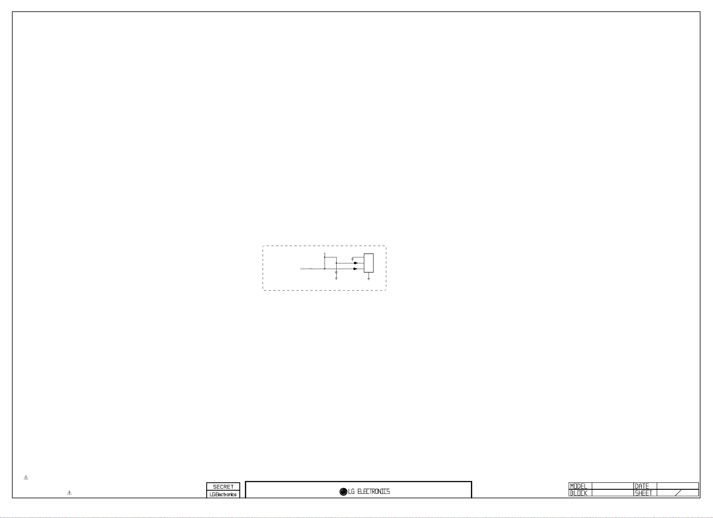
SPDIF
Copyright © 2014 LG Electronics. Inc. All rights reserved.
Only for training and service purposes
LGE Internal Use Only
SPDIF OUT
SPDIF_OUT
R3610
+3.3V_NORMAL
R3611
2.7K
OPT
33
C3602
0.1uF
16V
VINPUT
GND
Fiber Optic
1
VCC
2
JK3602
JST1223-001
3
4
FIX_POLE
THE SYMBOL MARK OF THIS SCHEMETIC DIAGRAM INCORPORATES
SPECIAL FEATURES IMPORTANT FOR PROTECTION FROM X-RADIATION.
FIRE AND ELECTRICAL SHOCK HAZARDS, WHEN SERVICING IF IS
ESSENTIAL THAT ONLY MANUFACTURES SPECIFIED PARTS BE USED FOR
THE CRITICAL COMPONENTS IN THE SYMBOL MARK OF THE SCHEMETIC.
JACK HIGH / MID
2011.11.21
36

KEY1
Copyright © 2014 LG Electronics. Inc. All rights reserved.
Only for training and service purposes
LGE Internal Use Only
KEY2
Place Near Micom
R4117
10K
5%
R4113
100
R4114
100
+3.5V_ST
R4118
10K
5%
LOGO_LIGHT
+3.5V_ST
+3.5V_ST
R4132
LOGO_LIGHT
10K
C4100
0.1uF
BLM18PG121SN1D
10K
OPT
R4133
C4120
0.1uF
16V
LOGO_LIGHT
C4102
0.1uF
D4100
5.6V
AMOTECH CO., LTD.
L4100
AMOTECH CO., LTD.
OPT
C4104
1000pF
50V
1K
R4134
LOGO_LIGHT
IR
D4101
5.6V
OPT
LED_R
LOGO_LIGHT
Q4100
MMBT3904(NXP)
+3.5V_ST
R4107
10K
B
R4125 10K
C
E
C4107
100pF
50V
LED_R
R4131
22
LOGO_LIGHT
D4104
5.6V
EYE_SCL
EYE_Q_10P
EYE_SDA
EYE_Q_10P
OPT
AMOTECH CO., LTD.
R4137
100
D4105
ADMC 5M 02 200L
OPT
R4138
100
D4106
ADMC 5M 02 200L
OPT
KEY1
KEY2
+3.5V_ST
LOGO/LED_R
12507WR-08L
12507WR-10L
GND
GND
IR
GND
NON_EYE_Q_8P
P4101
P4102
1
1
2
2
3
3
4
4
5
5
6
6
7
7
8
8
9
9
10
EYE_Q_10P
11
P4100
12507WR-06L
WIFI
7
L4111
MAX 0.4A
C4113
C4112
10uF
10uF
10V
10V
WIFI
WIFI
1
2
3
4
5
6
ZD4100
ADLC 5S 02 015
WIFI_ESD
22
R4130
OPT
22
R4136
WIFI
BLM18PG121SN1D
C4111
0.1uF
16V
WIFI
For EMI
WIFI_DM
WIFI_DP
ZD4101
ADLC 5S 02 015
WIFI_ESD
WOL/ETH_POWER_ON
WOL/WIFI_POWER_ON
WIFI
+3.5V_ST_WAKE
TP4100
TP4101
TP4102
TP4103
TP4104
RTS
M_REMOTE_RX
M_REMOTE_TX
M_RFModule_RESET
CTS
THE SYMBOL MARK OF THIS SCHEMETIC DIAGRAM INCORPORATES
SPECIAL FEATURES IMPORTANT FOR PROTECTION FROM X-RADIATION.
FIRE AND ELECTRICAL SHOCK HAZARDS, WHEN SERVICING IF IS
ESSENTIAL THAT ONLY MANUFACTURES SPECIFIED PARTS BE USED FOR
THE CRITICAL COMPONENTS IN THE SYMBOL MARK OF THE SCHEMETIC.
IR / KEY
2011.11.21
41
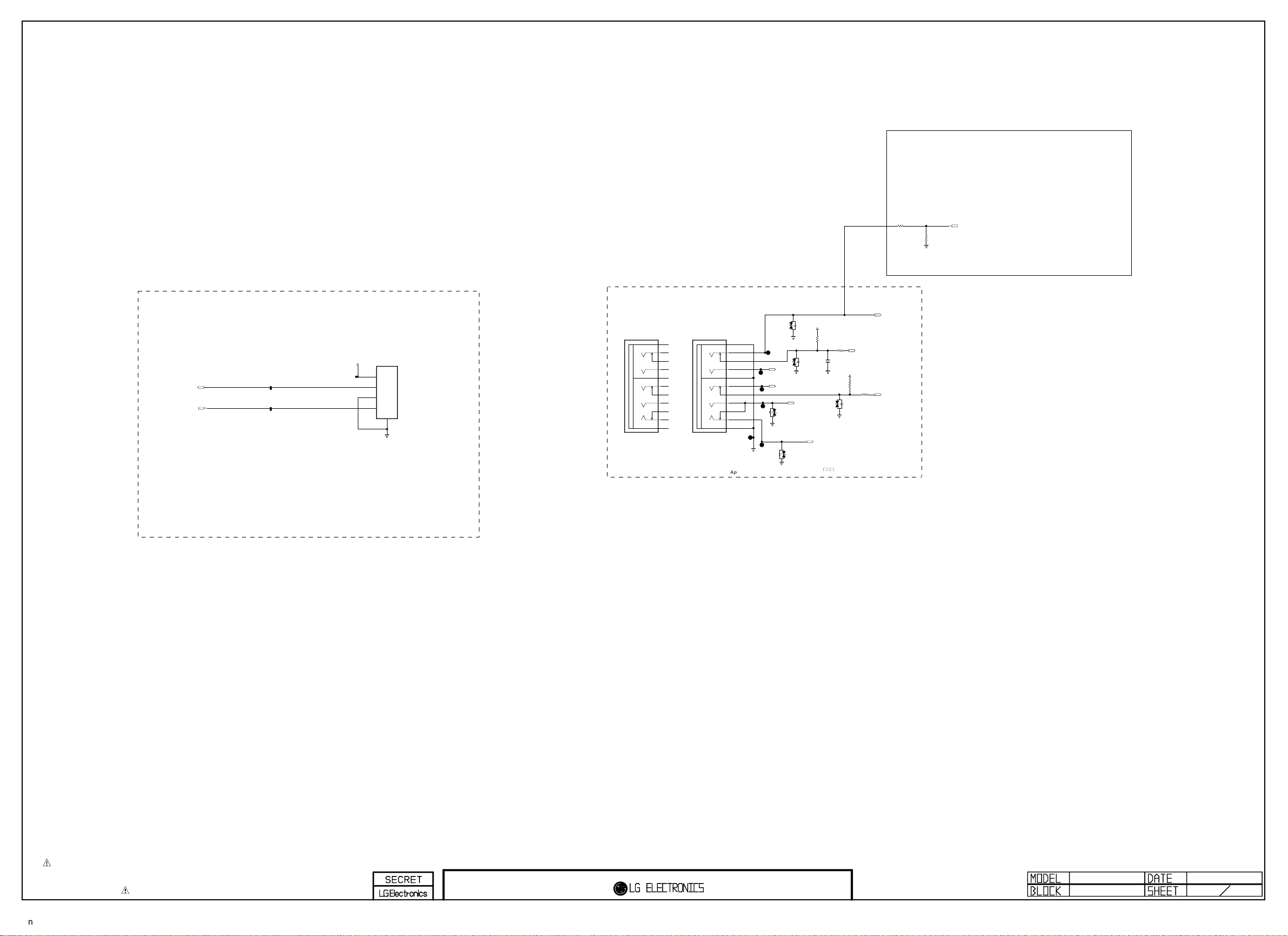
DEBUG FOR INTERNAL AMOD.
Copyright © 2014 LG Electronics. Inc. All rights reserved.
Only for training and service purposes
LGE Internal Use Only
OPT
R3801
0
TU_DEBUG
R3800
75
1%
DTV/MNT_V_OUT_SOC
For TU_Debug
Disconnet R374
UART FOR DEBUG
SOC_RX
SOC_TX
+3.5V_ST
UART_4PIN_STRAIGHT
P3800
12507WS-04L
1
2
3
4
5
AV/COMPONENT REAR
Mold_AV
PPJ245N2-01
JK3800-*1
7A
[GN/YL]E-LUG
6A
[GN/YL]O-SPRING
4A
[GN/YL]CONTACT
5B
[BL]O-SPRING
8C
[RD1]E-LUG-S
6C
[RD1]O-SPRING
4C
[RD1]CONTACT
5D
[WH]O-SPRING
4E
[RD2]CONTACT
6E
[RD2]O-SPRING
7E
[RD2]E-LUG
NON_Mold_AV
PPJ245-01
JK3800
7A
6A
4A
5B
8C
6C
4C
5D
4E
6E
7E
+3.3V_NORMAL
ZD3804
ADUC 5S 02 0R5L
OPT
R3806
D3803
5.6V
AV_COMP_ESD
COMP1/AV1/DVI_L_IN
D3802
5.6V
10K
R3811
1K
C3800
0.1uF
16V
COMP1/AV1/DVI_R_IN
+3.3V_NORMAL
R3810
10K
D3800
5.6V
AV_COMP_ESD
[GN]E-LUG
[GN]C-SPRING
[GN]CONTACT
[BL]C-SPRING
[RD1]E-LUG-S
[RD1]C-SPRING
[RD1]CONTACT
[WH]C-SPRING
[RD2]CONTACT
[RD2]C-SPRING
[RD2]E-LUG
COMP1_Pb
COMP1_Pr
D3801
5.6V
AV_COMP_ESD
AV_COMP_ESD
Apply "AV_COMP_ESD" when your model’s ESD Test is failed
AV1_CVBS_DET
R3812
1K
COMP1_Y/AV1_CVBS
COMP1_DET
THE SYMBOL MARK OF THIS SCHEMETIC DIAGRAM INCORPORATES
SPECIAL FEATURES IMPORTANT FOR PROTECTION FROM X-RADIATION.
FIRE AND ELECTRICAL SHOCK HAZARDS, WHEN SERVICING IF IS
ESSENTIAL THAT ONLY MANUFACTURES SPECIFIED PARTS BE USED FOR
THE CRITICAL COMPONENTS IN THE SYMBOL MARK OF THE SCHEMETIC.
JACK_COMMON
2011.11.21
38
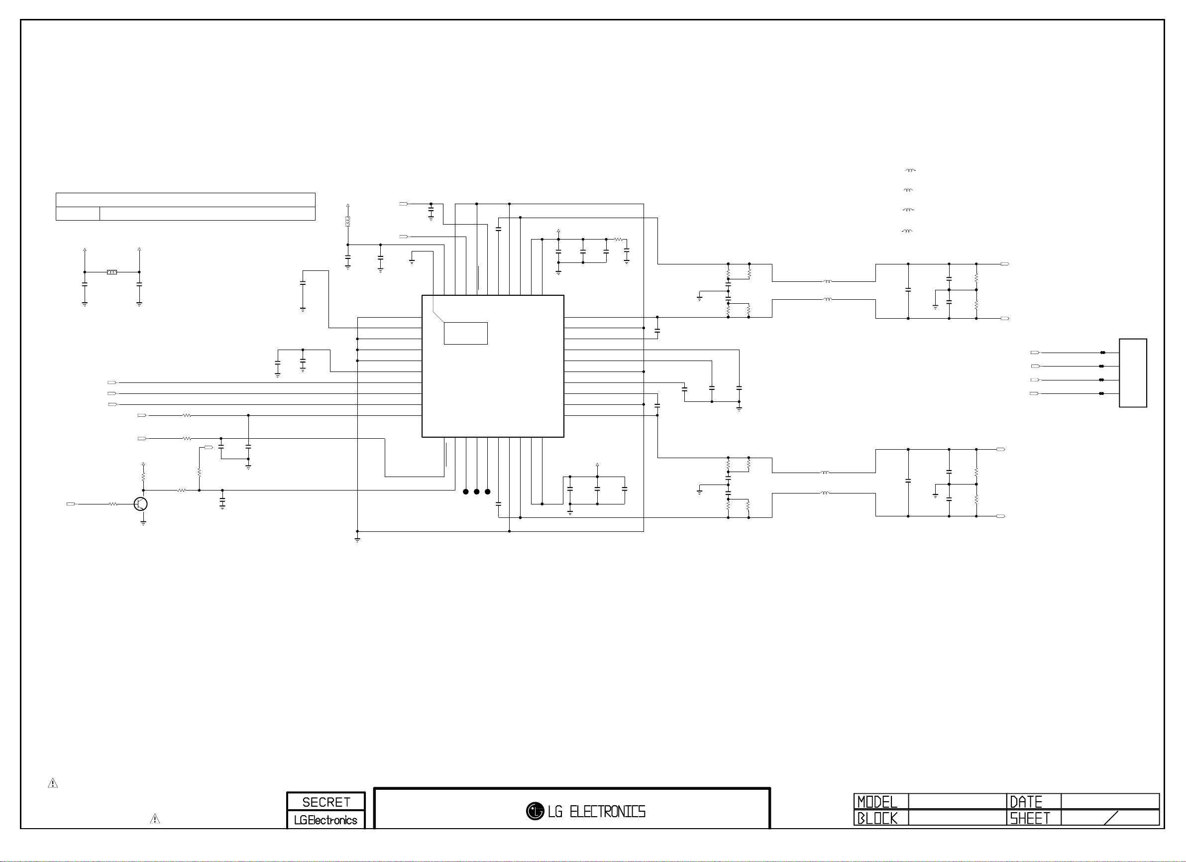
AMP_MUTE
Copyright © 2014 LG Electronics. Inc. All rights reserved.
Only for training and service purposes
LGE Internal Use Only
Q1801
DUAL COMPONENT
1ST : 0TRIY80001A 2ND : 0TR387500AA
R5400
L5400
+24V_AMP
I2C_SDA1
I2C_SCL1
+3.3V_NORMAL
10K
C5401
0.1uF
50V
C
B
E
+24V
UBW2012-121F
C5400
0.1uF
50V
AUD_LRCH
AUD_LRCK
AUD_SCK
AMP_MUTE_MICOM
R5402 100
R5403 100
AMP_MUTE_MICOM
R5401
10K
R5405
AMP_MUTE_MICOM
Q5400
MMBT3904(NXP)
AMP_MUTE_MICOM
POWER_DET
100
100
R5419
AMP_MUTE_PWR_DET
C5404
1000pF
50V
C5406
33pF
50V
C5408
33pF
50V
L5404-*1
10.0uH
L5405-*1
10.0uH
L5402-*1
10.0uH
L5403-*1
10.0uH
Audio_Coil_TAIYO
Audio_Coil_TAIYO
Audio_Coil_TAIYO
C5434
0.47uF
50V
C5435
0.47uF
50V
Audio_Coil_TAIYO
C5436
0.1uF
50V
C5437
0.1uF
50V
C5438
0.1uF
50V
C5439
0.1uF
50V
R5415
5.1K
R5416
5.1K
R5417
5.1K
R5418
5.1K
SPK_L+
SPEAKER_L
SPK_L-
SPK_L+
SPK_L-
SPK_R+
SPK_R-
SPK_R+
SPEAKER_R
SPK_R-
WAFER-ANGLE
4
3
2
1
P5400
NRS6045T100MMGK
+3.3V_NORMAL
L5401
BLM18PG121SN1D
C5413
0.1uF
16V
C5411
0.1uF
16V
OPT
C5440
C5412
0.1uF
1uF
16V
10V
AMP_RESET_N
AUD_MASTER_CLK
C5414
10uF
10V
AGND_PLL
VDD_PLL
DGND_PLL
GND
DGND
DVDD
SDATA
WCK
BCK
SDA
C5415
1000pF
50V
VDD_IO
[EP]GND
40
1
2
THERMAL
3
4
5
6
7
8
9
10
11
SCL
AD
CLK_I
GND_IO
37
38
39
41
NTP7513
12
13
14
FAULT
MONITOR_0
MONITOR_1
50V
C5416
BST1A
RESET
35
36
IC5400
0x54
15
16
BST2B
MONITOR_2
C5417
22000pF
50V
22000pF
OUT1A
PGND1A
33
34
17
18
OUT2B
PGND2B
+24V_AMP
PVDD1B
PVDD1A
31
32
30
29
28
27
26
25
24
23
22
21
19
PVDD2B20PVDD2A
C5418
0.1uF
50V
OUT1B
PGND1B
BST1B
VDR1
VCC5
AGND
VDR2
BST2A
PGND2A
OUT2A
C5419
0.1uF
50V
C5420
0.1uF
50V
+24V_AMP
C5421
0.1uF
50V
R5406
3.3
C5422
10uF
35V
OPT
OPT
C5424
0.01uF
50V
R5407
C5423
10uF
35V
C5425
22000pF
50V
C5426
22000pF
50V
C54 27
1uF
10V
C54 28
1uF
10V
12
C5429
390pF
50V
C5430
390pF
50V
R5408
12
R5409
12
C5431
390pF
50V
C5432
390pF
50V
R5410
12
C5433
1uF
10V
R5414
12
R5412
12
R5413
12
R5411
12
L5404
10uH
LPH6045T-100M
L5405
10uH
LPH6045T-100M
L5402
10uH
LPH6045T-100M
L5403
10uH
LPH6045T-100M
Audio_Coil_ABCO
Audio_Coil_ABCO
Audio_Coil_ABCO
Audio_Coil_ABCO
NRS6045T100MMGK
NRS6045T100MMGK
NRS6045T100MMGK
[AMP_MUTE_PWR_DET]
-->For fixing AC-OFF POP noise 32"POLA/ROW model
-->32"POLA/ROW LPB’s 3.5st drop time is very fast
THE SYMBOL MARK OF THIS SCHEMETIC DIAGRAM INCORPORATES
SPECIAL FEATURES IMPORTANT FOR PROTECTION FROM X-RADIATION.
FIRE AND ELECTRICAL SHOCK HAZARDS, WHEN SERVICING IF IS
ESSENTIAL THAT ONLY MANUFACTURES SPECIFIED PARTS BE USED FOR
THE CRITICAL COMPONENTS IN THE SYMBOL MARK OF THE SCHEMETIC.
AMP_NEO
2011.11.21
54

EARPHONE AMP
Copyright © 2014 LG Electronics. Inc. All rights reserved.
Only for training and service purposes
LGE Internal Use Only
HP_OUT_H13
C6104-*1
18pF
IC6100
TPA6138A2
HP_OUT_H13
C6109-*1
18pF
HP_ROUT_MAIN
HP_OUT_H13
R6103-*1
43K
1%
C6100
1uF
10V
HP_OUT
HP_ROUT_AMP
SIDE_HP_MUTE
HP_OUT
R6100
10K
HP_OUT_MTK
C6104
180pF
R6103
33K
+3.3V_NORMAL
HP_OUT_MTK
HP_OUT
R6106
43K
1%
4.7K
R6105
HP_OUT
HP_OUT
HP_OUT
C6102
1uF
10V
C6108
10pF
50V
+INR
-INR
OUTR
GND_1
MUTE
VSS
10V
+INL
14
-INL
13
12
11
10
HP_OUT
OUTL
UVP
GND_2
VDD
9
CP
8
1
HP_OUT
2
3
4
5
6
CN
7
C6103
1uF
HP_OUT
C6106
10pF
50V
HP_OUT_MTK
HP_OUT
R6104
43K
1%
+3.3V_NORMAL
HP_OUT
HP_OUT
C6109
180pF
R6102
33K
HP_OUT_MTK
L6100
120-ohm
BLM18P G12 1SN1D
HP_OUT
C6105
1uF
10V
C6107
0.1uF
16V
HP_OUT
R6101
10K
C6101
1uF
10V
HP_OUT
HP_LOUT_AMP
HP_LOUT_MAIN
HP_OUT_H13
R6102-*1
43K
1%
THE SYMBOL MARK OF THIS SCHEMETIC DIAGRAM INCORPORATES
SPECIAL FEATURES IMPORTANT FOR PROTECTION FROM X-RADIATION.
FIRE AND ELECTRICAL SHOCK HAZARDS, WHEN SERVICING IF IS
ESSENTIAL THAT ONLY MANUFACTURES SPECIFIED PARTS BE USED FOR
THE CRITICAL COMPONENTS IN THE SYMBOL MARK OF THE SCHEMETIC.
HEADPHONE AMP
2011.09.29
61
 Loading...