

LG 49UB850T-DA Schematic
Internal Use Only
North/Latin America http://aic.lgservice.com
Europe/Africa http://eic.lgservice.com
Asia/Oceania http://biz.lgservice.com
LED TV
SERVICE MANUAL
CHASSIS : LT41V
MODEL : 49UB850T 49UB850T-DA
CAUTION
BEFORE SERVICING THE CHASSIS,
READ THE SAFETY PRECAUTIONS IN THIS MANUAL.
Printed in KoreaP/NO : MFL68140404 (1404-REV00)

CONTENTS
CONTENTS .............................................................................................. 2
PRODUCT SAFETY ................................................................................. 3
SPECIFICATION ....................................................................................... 6
ADJUSTMENT INSTRUCTION .............................................................. 16
EXPLODED VIEW .................................................................................. 28
SCHEMATIC CIRCUIT DIAGRAM ..............................................................
Only for training and service purposes
- 2 -
LGE Internal Use OnlyCopyright © LG Electronics. Inc. All rights reserved.
SAFETY PRECAUTIONS
IMPORTANT SAFETY NOTICE
Many electrical and mechanical parts in this chassis have special safety-related characteristics. These parts are identified by in the
Schematic Diagram and Exploded View.
It is essential that these special safety parts should be replaced with the same components as recommended in this manual to prevent
Shock, Fire, or other Hazards.
Do not modify the original design without permission of manufacturer.
General Guidance
An isolation Transformer should always be used during the
servicing of a receiver whose chassis is not isolated from the AC
power line. Use a transformer of adequate power rating as this
protects the technician from accidents resulting in personal injury
from electrical shocks.
It will also protect the receiver and it's components from being
damaged by accidental shorts of th e cir cuitry that may be
inadvertently introduced during the service operation.
If any fuse (or Fusible Resistor) in this TV receiver is blown,
replace it with the specified.
When replacing a high wattage resistor (Oxide Metal Film Resistor,
over 1 W), keep the resistor 10 mm away from PCB.
Keep wires away from high voltage or high temperature parts.
Before returning the receiver to the customer,
always perform an AC leakage current check on the exposed
metallic parts of the cabinet, such as antennas, terminals, etc., to
be sure the set is safe to operate without damage of electrical
shock.
Leakage Current Cold Check(Antenna Cold Check)
With the instrument AC plug removed from AC source, connect an
electrical jumper across the two AC plug prongs. Place the AC
switch in the on position, connect one lead of ohm-meter to the AC
plug prongs tied together and touch other ohm-meter lead in turn to
each exposed metallic parts such as antenna terminals, phone
jacks, etc.
If the exposed metallic part has a return path to the chassis, the
measured resistance should be between 1 MΩ and 5.2 MΩ.
When the exposed metal has no return path to the chassis the
reading must be infinite.
An other abnormality exists that must be corrected before the
receiver is returned to the customer.
Leakage Current Hot Check (See below Figure)
Plug the AC cord directly into the AC outlet.
Do not use a line Isolation Transformer during this check.
Connect 1.5 K / 10 watt resistor in parallel with a 0.15 uF capacitor
between a known good earth ground (Water Pipe, Conduit, etc.)
and the exposed metallic parts.
Measure the AC voltage across the resistor using AC voltmeter
with 1000 ohms/volt or more sensitivity.
Reverse plug the AC cord into the AC outlet and repeat AC voltage
measurements for each exp ose d metallic par t. Any voltage
measured must not exceed 0.75 volt RMS which is corresponds to
0.5 mA.
In case any measurement is out of the limits specified, there is
possibility of shock hazard and the set must be checked and
repaired before it is returned to the customer.
Leakage Current Hot Check circuit
Only for training and service purposes
- 3 -
LGE Internal Use OnlyCopyright © LG Electronics. Inc. All rights reserved.

SERVICING PRECAUTIONS
CAUTION: Before servicing receivers covered by this service
manual and its supplements and addenda, read and follow the
SAFETY PRECAUTIONS on page 3 of this publication.
NOTE: If unforeseen circumstances create conict between the
following servicing precautions and any of the safety precautions
on page 3 of this publication, always follow the safety precautions.
Remember: Safety First.
General Servicing Precautions
1. Always unplug the receiver AC power cord from the AC power
source before;
a. Removing or reinstalling any component, circuit board mod-
ule or any other receiver assembly.
b. Disconnecting or reconnecting any receiver electrical plug or
other electrical connection.
c. Connecting a test substitute in parallel with an electrolytic
capacitor in the receiver.
CAUTION: A wrong part substitution or incorrect polarity
installation of electrolytic capacitors may result in an explosion hazard.
2. Test high voltage only by measuring it with an appropriate
high voltage meter or other voltage measuring device (DVM,
FETVOM, etc) equipped with a suitable high voltage probe.
Do not test high voltage by "drawing an arc".
3. Do not spray chemicals on or near this receiver or any of its
assemblies.
4. Unless specied otherwise in this service manual, clean
electrical contacts only by applying the following mixture to the
contacts with a pipe cleaner, cotton-tipped stick or comparable
non-abrasive applicator; 10 % (by volume) Acetone and 90 %
(by volume) isopropyl alcohol (90 % - 99 % strength)
CAUTION: This is a ammable mixture.
Unless specied otherwise in this service manual, lubrication of
contacts in not required.
5. Do not defeat any plug/socket B+ voltage interlocks with which
receivers covered by this service manual might be equipped.
6. Do not apply AC power to this instrument and/or any of its
electrical assemblies unless all solid-state device heat sinks are
correctly installed.
7. Always connect the test receiver ground lead to the receiver
chassis ground before connecting the test receiver positive
lead.
Always remove the test receiver ground lead last.
8. Use with this receiver only the test xtures specied in this
service manual.
CAUTION: Do not connect the test xture ground strap to any
heat sink in this receiver.
Electrostatically Sensitive (ES) Devices
Some semiconductor (solid-state) devices can be damaged easily by static electricity. Such components commonly are called
Electrostatically Sensitive (ES) Devices. Examples of typical ES
devices are integrated circuits and some eld-effect transistors
and semiconductor “chip” components. The following techniques
should be used to help reduce the incidence of component damage caused by static by static electricity.
1. Immediately before handling any semiconductor component or
semiconductor-equipped assembly, drain off any electrostatic
charge on your body by touching a known earth ground. Alternatively, obtain and wear a commercially available discharging
wrist strap device, which should be removed to prevent potential shock reasons prior to applying power to the unit under test.
2. After removing an electrical assembly equipped with ES
devices, place the assembly on a conductive surface such as
aluminum foil, to prevent electrostatic charge buildup or exposure of the assembly.
3. Use only a grounded-tip soldering iron to solder or unsolder ES
devices.
4. Use only an anti-static type solder removal device. Some solder
removal devices not classied as “anti-static” can generate
electrical charges sufcient to damage ES devices.
5. Do not use freon-propelled chemicals. These can generate
electrical charges sufcient to damage ES devices.
6. Do not remove a replacement ES device from its protective
package until immediately before you are ready to install it.
(Most replacement ES devices are packaged with leads electrically shorted together by conductive foam, aluminum foil or
comparable conductive material).
7. Immediately before removing the protective material from the
leads of a replacement ES device, touch the protective material
to the chassis or circuit assembly into which the device will be
installed.
CAUTION: Be sure no power is applied to the chassis or circuit,
and observe all other safety precautions.
8. Minimize bodily motions when handling unpackaged replacement ES devices. (Otherwise harmless motion such as the
brushing together of your clothes fabric or the lifting of your
foot from a carpeted oor can generate static electricity sufcient to damage an ES device.)
General Soldering Guidelines
1. Use a grounded-tip, low-wattage soldering iron and appropriate
tip size and shape that will maintain tip temperature within the
range or 500 °F to 600 °F.
2. Use an appropriate gauge of RMA resin-core solder composed
of 60 parts tin/40 parts lead.
3. Keep the soldering iron tip clean and well tinned.
4. Thoroughly clean the surfaces to be soldered. Use a mall wirebristle (0.5 inch, or 1.25 cm) brush with a metal handle.
Do not use freon-propelled spray-on cleaners.
5. Use the following unsoldering technique
a. Allow the soldering iron tip to reach normal temperature.
(500 °F to 600 °F)
b. Heat the component lead until the solder melts.
c. Quickly draw the melted solder with an anti-static, suction-
type solder removal device or with solder braid.
CAUTION: Work quickly to avoid overheating the circuit
board printed foil.
6. Use the following soldering technique.
a. Allow the soldering iron tip to reach a normal temperature
(500 °F to 600 °F)
b. First, hold the soldering iron tip and solder the strand against
the component lead until the solder melts.
c. Quickly move the soldering iron tip to the junction of the
component lead and the printed circuit foil, and hold it there
only until the solder ows onto and around both the component lead and the foil.
CAUTION: Work quickly to avoid overheating the circuit
board printed foil.
d. Closely inspect the solder area and remove any excess or
splashed solder with a small wire-bristle brush.
Only for training and service purposes
- 4 -
LGE Internal Use OnlyCopyright © LG Electronics. Inc. All rights reserved.

IC Remove/Replacement
Some chassis circuit boards have slotted holes (oblong) through
which the IC leads are inserted and then bent at against the circuit foil. When holes are the slotted type, the following technique
should be used to remove and replace the IC. When working with
boards using the familiar round hole, use the standard technique
as outlined in paragraphs 5 and 6 above.
Removal
1. Desolder and straighten each IC lead in one operation by
gently prying up on the lead with the soldering iron tip as the
solder melts.
2. Draw away the melted solder with an anti-static suction-type
solder removal device (or with solder braid) before removing
the IC.
Replacement
1. Carefully insert the replacement IC in the circuit board.
2. Carefully bend each IC lead against the circuit foil pad and
solder it.
3. Clean the soldered areas with a small wire-bristle brush.
(It is not necessary to reapply acrylic coating to the areas).
"Small-Signal" Discrete Transistor
Removal/Replacement
1. Remove the defective transistor by clipping its leads as close
as possible to the component body.
2. Bend into a "U" shape the end of each of three leads remaining
on the circuit board.
3. Bend into a "U" shape the replacement transistor leads.
4. Connect the replacement transistor leads to the corresponding
leads extending from the circuit board and crimp the "U" with
long nose pliers to insure metal to metal contact then solder
each connection.
Power Output, Transistor Device
Removal/Replacement
1. Heat and remove all solder from around the transistor leads.
2. Remove the heat sink mounting screw (if so equipped).
3. Carefully remove the transistor from the heat sink of the circuit
board.
4. Insert new transistor in the circuit board.
5. Solder each transistor lead, and clip off excess lead.
6. Replace heat sink.
Diode Removal/Replacement
1. Remove defective diode by clipping its leads as close as possible to diode body.
2. Bend the two remaining leads perpendicular y to the circuit
board.
3. Observing diode polarity, wrap each lead of the new diode
around the corresponding lead on the circuit board.
4. Securely crimp each connection and solder it.
5. Inspect (on the circuit board copper side) the solder joints of
the two "original" leads. If they are not shiny, reheat them and if
necessary, apply additional solder.
3. Solder the connections.
CAUTION: Maintain original spacing between the replaced
component and adjacent components and the circuit board to
prevent excessive component temperatures.
Circuit Board Foil Repair
Excessive heat applied to the copper foil of any printed circuit
board will weaken the adhesive that bonds the foil to the circuit
board causing the foil to separate from or "lift-off" the board. The
following guidelines and procedures should be followed whenever
this condition is encountered.
At IC Connections
To repair a defective copper pattern at IC connections use the
following procedure to install a jumper wire on the copper pattern
side of the circuit board. (Use this technique only on IC connections).
1. Carefully remove the damaged copper pattern with a sharp
knife. (Remove only as much copper as absolutely necessary).
2. carefully scratch away the solder resist and acrylic coating (if
used) from the end of the remaining copper pattern.
3. Bend a small "U" in one end of a small gauge jumper wire and
carefully crimp it around the IC pin. Solder the IC connection.
4. Route the jumper wire along the path of the out-away copper
pattern and let it overlap the previously scraped end of the
good copper pattern. Solder the overlapped area and clip off
any excess jumper wire.
At Other Connections
Use the following technique to repair the defective copper pattern
at connections other than IC Pins. This technique involves the
installation of a jumper wire on the component side of the circuit
board.
1. Remove the defective copper pattern with a sharp knife.
Remove at least 1/4 inch of copper, to ensure that a hazardous
condition will not exist if the jumper wire opens.
2. Trace along the copper pattern from both sides of the pattern
break and locate the nearest component that is directly connected to the affected copper pattern.
3. Connect insulated 20-gauge jumper wire from the lead of the
nearest component on one side of the pattern break to the lead
of the nearest component on the other side.
Carefully crimp and solder the connections.
CAUTION: Be sure the insulated jumper wire is dressed so the
it does not touch components or sharp edges.
Fuse and Conventional Resistor
Removal/Replacement
1. Clip each fuse or resistor lead at top of the circuit board hollow
stake.
2. Securely crimp the leads of replacement component around
notch at stake top.
Only for training and service purposes
- 5 -
LGE Internal Use OnlyCopyright © LG Electronics. Inc. All rights reserved.

SPECIFICATION
NOTE : Specifications and others are subject to change without notice for improvement
.
1. Application range
This spec sheet is applied to the LED TV used LT41V, LT41U
chassis
2. Test condition
Each part is tested as below without special notice.
1) Temperature : 25 ºC ± 5 ºC(77±9ºF), CST : 40 ºC±5 ºC
2) Relative Humidity: 65 % ± 10 %
3) Power Voltage
Standard input voltage (100~240V@ 50/60Hz)
* Standard Voltage of each products is marked by models.
4) Specification and performance of each parts are followed
ea ch drawing and s pe cificatio n b y p art number in
accordance with BOM.
5) The receiver must be operated for about 20 minutes prior to
the adjustment.
3. Test method
1) Performance: LGE TV test method followed
2) Demanded other specification
- Safety : CE, IEC specification
- EMC: CE, IEC
Only for training and service purposes
- 6 -
LGE Internal Use OnlyCopyright © LG Electronics. Inc. All rights reserved.
4. General Specification
No Item Specication Remark
1. Display Screen Device 65” wide Color Display Module Resolution: 3840*2160
55” wide Color Display Module
49” wide Color Display Module
84” wide Color Display Module
79” wide Color Display Module
2. Aspect Ratio 16:9 All
3. LCD Module 65" QWUXGA TFT LCD 65UB98(LC650EQF-FGF1),
79" QWUXGA TFT LCD LC790EQF-FGF1
84” TFT WUXGA LCD LC840EQD-SGF1
55" QWUXGA TFT LCD LC550EQE-PGF2
49" QWUXGA TFT LCD LC790EQF-FGF1
4. Operating Environment TFT Temp. : 0 ~ 50 deg
5. Storage Environment TFT Temp. : -20 ~ 60 deg
6. Input Voltage AC100 ~ 240V, 50/60Hz
7. Power Consumption(Typ) T240
Advance
Cinema
T120
Advance
Cinema
8. LCD Module Size Maker Inch (H)mm × (V)mm × (D)mm
LGD 65” 1443.4.0 × 821.6 × 12.2
Pixel Pitch Maker Inch mm x mm
LGD 65” 0.372 × 0.372
Back Light LGD 49”/55”
Display Colors 1.06 Billion Colors @ 10bit(D)
Coating Hard coating(2H), Anti-glare treatment
Humidity : 10 ~ 90%
Humidity : 10 ~ 90%
Temp. : -20 ~ 60 deg
Humidity : 5 ~ 90%RH
65" 155.1 W Logic=16.8W, BackLight=138.3W)
79” 165.6 W
84” 402 W
55” 111.5 W
49” 97.1 W
79” 1759.4 x 1002.4 x13.9
84” 1904.0 x 1096.0 x 15.5
55” 1226.0 x 702.1 x 9.2
49” 1086.3 x 623.8 x 10.6
79” 0.453 x 0.453
84” 0.4845x0.4845
55” 0.315 x 0.315
49” 0.27963 x 0.27963
ULTRA HD
/65”/79”
/84”
65UB93(LC650EQF-FGM1)
LGE SPEC
Only 84” , LGD SPEC
LGE SPEC
Only for training and service purposes
- 7 -
LGE Internal Use OnlyCopyright © LG Electronics. Inc. All rights reserved.
5. External Input Support Format
5.1. Component (Y, PB, PR)
No Resolution H-freq(kHz) V-freq.(kHz) Pixel clock Proposed
1. 720*480i 15.73 59.94 13.500 SDTV, DVD 480I(525I)
2. 720*480i 15.73 60.00 13.514 SDTV, DVD 480I(525I)
3. 720*576i 15.625 50.00 13.500 SDTV, DVD 576I(625I) 50Hz
4. 720*480p 31.47 59.94 27.000 SDTV 480P
5. 720*480p 31.50 60.00 27.027 SDTV 480P
6. 720*576p 31.25 50.00 27.000 SDTV 576P 50Hz
7. 1280*720 44.96 59.94 74.176 HDTV 720P
8. 1280*720 45.00 60.00 74.250 HDTV 720P
9. 1280*720 37.50 50.00 74.25 HDTV 720P 50Hz
10. 1920*1080 28.125 50.00 74.250 HDTV 1080I 50Hz,
11. 1920*1080 33.72 59.94 74.176 HDTV 1080I
12. 1920*1080 33.75 60.00 74.25 HDTV 1080I
13. 1920*1080 26.97 23.976 63.296 HDTV 1080P
14. 1920*1080 27.00 24.000 63.36 HDTV 1080P
15. 1920*1080 33.71 29.97 79.120 HDTV 1080P
16. 1920*1080 33.75 30.00 79.20 HDTV 1080P
17. 1920*1080 56.25 50 148.5 HDTV 1080P
18. 1920*1080 67.432 59.94 148.350 HDTV 1080P
19. 1920*1080 67.5 60.00 148.5 HDTV 1080P
Only for training and service purposes
- 8 -
LGE Internal Use OnlyCopyright © LG Electronics. Inc. All rights reserved.
5.2. HDMI : EDID DATA : Refer to adjust specification
5.2.1. DTV mode
No Resolution H-freq(kHz) V-freq.(Hz)
1 640*480 31.469 59.94 25.125 SDTV 480P
2 640*480 31.5 60 25.125 SDTV 480P
3 720*480 15.73 59.94 13.500 SDTV, DVD 480I(525I) Spec. out but display
4 720*480 15.75 60.00 13.514 SDTV, DVD 480I(525I)
5 720*576 15.625 50.00 13.500 SDTV, DVD 576I(625I) 50Hz
6 720*480 31.47 59.94 27 SDTV 480P
7 720*480 31.5 60.00 27.027 SDTV 480P
8 720*576 31.25 50.00 27 SDTV 576P
9 1280*720 44.96 59.94 74.176 HDTV 720P
10 1280*720 45 60.00 74.25 HDTV 720P
11 1280*720 37.5 50.00 74.25 HDTV 720P
12 1920*1080 28.125 50.00 74.25 HDTV 1080I
13 1920*1080 33.72 59.94 74.176 HDTV 1080I
14 1920*1080 33.75 60.00 74.25 HDTV 1080I
15 1920*1080 26.97 23.976 63.296 HDTV 1080P
16 1920*1080 27.00 24.000 63.36 HDTV 1080P
17 1920*1080 28.125 25 74.25 HDTV 1080P
18 1920*1080 33.71 29.97 79.120 HDTV 1080P
19 1920*1080 33.75 30.00 79.20 HDTV 1080P
20 1920*1080 56.25 50.00 148.5 HDTV 1080P
21 1920*1080 67.432 59.94 148.350 HDTV 1080P
22 1920*1080 67.5 60 148.50 HDTV 1080P
23 3840*2160 53.95 23.98 297.00 UDTV 2160P Only UD Model
24 3840*2160 54 24.00 297.00 UDTV 2160P Only UD Model
25 3840*2160 56.25 25.00 297.00 UDTV 2160P Only UD Model
26 3840*2160 61.43 29.97 297.00 UDTV 2160P Only UD Model
27 3840*2160 67.5 30.00 297.00 UDTV 2160P Only UD Model
28 3840*2160 112.5 50 594 UDTV 2160P Only UD Model, Port3
29 3840*2160 135 60 594 UDTV 2160P Only UD Model, Port3
30 3840*2160 135 59.94 594 UDTV 2160P Only UD Model, Port3
31 4096*2160 53.95 23.98 297 UDTV 2160P Only UD Model
32 4096*2160 54 24.00 297 UDTV 2160P Only UD Model
33 4096*2160 56.25 25.00 297 UDTV 2160P Only UD Model
34 4096*2160 61.43 29.97 297 UDTV 2160P Only UD Model
35 4096*2160 67.5 30.00 297 UDTV 2160P Only UD Model
36 4096*2160 112.5 50.00 594 UDTV 2160P Only UD Model, Port3
37 4096*2160 135 60.00 594 UDTV 2160P Only UD Model, Port3
38 4096*2160 135 59.94 594 UDTV 2160P Only UD Model, Port3
Pixel
clock(MHz)
Proposed Remark
Only for training and service purposes
- 9 -
LGE Internal Use OnlyCopyright © LG Electronics. Inc. All rights reserved.
5.2.2. PC mode
No. Resolution H-freq(kHz) V-freq.(kHz) Pixel clock Proposed Remarks
1 640*350 @70Hz 31.468 70.09 25.17 EGA
2 720*400@70Hz 31.469 70.08 28.32 DOS
3 640*480@60Hz 31.469 59.94 25.17 VESA(VGA)
4 800*600 @60Hz 37.879 60.31 40 VESA(SVGA)
5 1024*768 @60Hz 48.363 60.00 65 VESA(XGA)
6 1152*864@60Hz 54.348 60.053 80 VESA
7 1280*1024 @60Hz 63.981 60.020 109.00 VESA(SXGA) Support to HDMI-PC
8 1360*768 @60Hz 47.712 60.015 85.5 VESA(WXGA)
9 1920*1080@60Hz 67.5 60 158.40 WUXGA(CEA 861D)
10 3840*2160@30Hz 67.5 30.00 297.00 UDTV 2160P Only UHD Model
11 3840*2160@25Hz 56.25 25.00 297.00 UDTV 2160P Only UHD Model
12 3840*2160@24Hz 54.0 24.00 297.00 UDTV 2160P Only UHD Model
13 4096*2160@30Hz 61.43 29.97 297.00 UDTV 2160P Only UHD Model
14 4096*2160@30Hz 67.5 30.00 297.00 UDTV 2160P Only UHD Model
15 4096*2160@25Hz 56.25 25.00 297.00 UDTV 2160P Only UHD Model
16 4096*2160@24Hz 53.95 23.97 297.00 UDTV 2160P Only UD Model, Port3
17 4096*2160@24Hz 54 24.00 297.00 UDTV 2160P Only UD Model, Port3
Only for training and service purposes
- 10 -
LGE Internal Use OnlyCopyright © LG Electronics. Inc. All rights reserved.
6. 3D mode-DTV/HDMI/USB
6.1. RF Input (3D supported mode manually)
No Resolution H-freq(kHz) V-freq.(Hz) Pixel clock(MHz) Proposed 3D input proposed mode
1 1280*720 37.500 50 74.25 HDTV 720P 2D to 3D, Side by Side, Top & Bottom
2 1920*1080 28.125 50 74.25 HDTV 1080I 2D to 3D, Side by Side, Top & Bottom
6.2. HDMI Input
6.2.1. RF Input (3D supported mode automatically)
No Resolution H-freq(kHz) V-freq.(Hz) Pixel clock(MHz) Proposed 3D input proposed mode
1 720*480 31.5 60 27.03 SDTV 480P 2D to 3D, Side by Side(Half),
2 720*576 31.25 50 27 SDTV 576P
3 1280*720 45.00 60.00 74.25 HDTV 720P
37.500 50 74.25 HDTV 720P
4 1920*1080 33.75 60.00 74.25 HDTV 1080I 2D to 3D, Side by Side(Half), Top & Bottom
28.125 50.00 74.25 HDTV 1080I
5 1920*1080 27.00 24.00 74.25 HDTV 1080P 2D to 3D, Side by Side(Half), Top & Bottom,
28.12 25 74.25 HDTV 1080P
33.75 30.00 74.25 HDTV 1080P
67.50 60.00 148.5 HDTV 1080P 2D to 3D, Side by Side(Half),
56.250 50 148.5 HDTV 1080P
6 3840*2160 53.95 23.976 297.00 HDTV 2160P 2D to 3D,
54 24.00 296.703
56.25 25.00 297.00
61.43 29.970 297.00
67.5 30.00 296.703
Top & Bottom, Checker Board,
Frame Sequential, Row Interleaving,
Column Interleaving
Checker Board, Row Interleaving, Column
Interleaving
Top & Bottom,
Checker Board, Single Frame Sequential,
Row Interleaving, Column Interleaving
Top & Bottom(half), Side by Side(half),
Only for training and service purposes
- 11 -
LGE Internal Use OnlyCopyright © LG Electronics. Inc. All rights reserved.
6.2.2. HDMI Input 1.4b (3D supported mode automatically)
No Resolution H-freq(kHz) V-freq.(Hz) Pixel clock
(MHz)
1 640*480 31.469 / 31.5 59.94/ 60 25.125/25.2 1 Top-and-Bottom
31.469 / 31.5 59.94/ 60 50.35/50.4 1 Side-by-side(Full) (SDTV 480P)
62.938/63 59.94/ 60 50.35/50.4 1 Frame packing
2 720*480 31.469 / 31.5 59.94 / 60 27.00/27.03 2,3 Top-and-Bottom
31.469 / 31.5 59.94 / 60 54/54.06 2,3 Side-by-side(Full) (SDTV 480P)
62.938/63 59.94 / 60 54/54.06 2,3 Frame packing
3 720*576 31.25 50 27 17,18 Top-and-Bottom
31.25 50 54 17,18 Side-by-side(Full) (SDTV 576P)
62.5 50 54 17,18 Frame packing
4 720*576 15.625 50 27 21 Frame packing
5 1280*720 37.500 50 74.25 19 Top-and-Bottom
37.500 50 148.5 19 Side-by-side(Full) (HDTV 720P)
44.96 / 45 59.94 / 60 74.17/74.25 4 Top-and-Bottom
44.96 / 45 59.94 / 60 148.35/148.5 4 Side-by-side(Full) (HDTV 720P)
75 50 148.5 19 Frame packing
89.91/90 59.94 / 60 148.35/148.5 4 Frame packing
6 1920*1080 28.125 50.00 74.25 20 Top-and-Bottom
VIC 3D input proposed
mode
Side-by-side(half)
Line alternative
Side-by-side(half)
Line alternative
Side-by-side(half)
Line alternative
Field alternative
Side-by-side(Full)
Top-and-Bottom
Side-by-side(half)
Side-by-side(half)
Side-by-side(half)
Line alternative
Line alternative
Side-by-side(half)
Proposed
Secondary(SDTV 480P)
Secondary(SDTV 480P)
Secondary(SDTV 480P)
(SDTV 480P)
Secondary(SDTV 480P)
Secondary(SDTV 480P)
Secondary(SDTV 480P)
(SDTV 480P)
Secondary(SDTV 576P)
Secondary(SDTV 576P)
Secondary(SDTV 576P)
(SDTV 576P)
Secondary(SDTV 576I)
(SDTV 576I
(SDTV 576I
Secondary(SDTV 576I)
Secondary(SDTV 576I)
Primary(HDTV 720P)
Primary(HDTV 720P)
Primary(HDTV 720P)
Primary(HDTV 720P)
Primary(HDTV 720P)
(HDTV 720P)
Primary(HDTV 720P)
(HDTV 720P)
Secondary(HDTV 1080I)
Primary(HDTV 1080I)
28.125 50.00 148.5 20 Side-by-side(Full) (HDTV 1080I)
33.72 / 33.75 59.94 / 60 74.17/74.25 5 Top-and-Bottom
33.72 / 33.75 59.94 / 60 148.35/148.5 5 Side-by-side(Full) (HDTV 1080I)
56.25 50.00 148.5 20 Frame packing
67.432/67.50 59.94 / 60 148.35/148.5 5 Frame packing
Only for training and service purposes
- 12 -
Side-by-side(half)
Field alternative
Field alternative
Secondary(HDTV 1080I)
Primary(HDTV 1080I)
Primary(HDTV 1080I)
(HDTV 1080I)
Primary(HDTV 1080I)
(HDTV 1080I)
LGE Internal Use OnlyCopyright © LG Electronics. Inc. All rights reserved.
No Resolution H-freq(kHz) V-freq.(Hz) Pixel clock
(MHz)
7 1920*1080 26.97 / 27 23.97 / 24 74.17/74.25 32 Top-and-Bottom
26.97 / 27 23.97 / 24 148.35/148.5 32 Side-by-side(Full) (HDTV 1080P)
28.125 25 74.25 33 Top-and-Bottom
28.125 25 148.5 33 Side-by-side(Full) (HDTV 1080P)
33.716 / 33.75 29.976 / 30.00 74.18/74.25 34 Top-and-Bottom
33.716 / 33.75 29.976 / 30.00 148.35/148.5 34 Side-by-side(Full) (HDTV 1080P)
43.94/54 23.97 / 24 148.35/148.5 32 Frame packing
56.25 25 148.5 33 Frame packing
67.432 / 67.5 29.976 / 30.00 148.35/148.5 34 Frame packing
56.250 50 148.5 31 Top-and-Bottom
67.432 / 67.5 59.94 / 60 148.35/148.50 16 Top-and-Bottom
VIC 3D input proposed
Side-by-side(half)
Side-by-side(half)
Side-by-side(half)
Line alternative
Line alternative
Line alternative
Side-by-side(half)
Side-by-side(half)
6.2.3. HDMI-PC 3D Input (3D supported mode manually)
mode
Proposed
Primary(HDTV 1080P)
Primary(HDTV 1080P)
Secondary(HDTV 1080P)
Secondary(HDTV 1080P)
Primary(HDTV 1080P)
Secondary(HDTV 1080P)
Primary(HDTV 1080P)
(HDTV 1080P)
Secondary(HDTV 1080P)
(HDTV 1080P)
Primary(HDTV 1080P)
(HDTV 1080P)
Primary(HDTV 1080P)
Secondary(HDTV 1080P)
Primary(HDTV 1080P)
Secondary(HDTV 1080P)
No Resolution H-freq(kHz) V-freq.(Hz) Pixel clock(MHz) 3D input proposed mode Proposed
1 1024*768 48.36 60 65 2D to 3D,
2 1360*768 47.71 60 85.5 2D to 3D,
3 1920*1080 67.500 60 148.50 2D to 3D, Side by Side(half),
4 3840*2160 54 24.00 296.703 2D to 3D,
56.25 25.00 297
67.5 30.00 296.703
5 3840*2160 135 60 594 2D to 3D,
6 4096*2160 135 60 594 2D to 3D,
7 Others - - - 2D to 3D,
Side by Side(half), Top & Bottom
Side by Side(half), Top & Bottom
Top & Bottom,Checker Board,
Single Frame Sequential,
Row Interleaving,
Column Interleaving
Top & Bottom(half),
Side by Side(half)
Top & Bottom(half),
Side by Side(half), Port 3 Only
Top & Bottom(half),
Side by Side(half), Port 3 Only
Side by Side(half), Top & Bottom
HDTV 768P
HDTV 768P
HDTV 1080P
HDTV 2160P
HDTV 2160P
HDTV 2160P
640*350
720*400
640*480
800*600
1152*864
Only for training and service purposes
- 13 -
LGE Internal Use OnlyCopyright © LG Electronics. Inc. All rights reserved.
6.2.4. Component 3D Input (3D supported mode manually)
No Resolution H-freq(kHz) V-freq.(Hz) Pixel clock(MHz) 3D input proposed mode Proposed
1 1280*720 37.5 50 74.25 2D to 3D,
Side by Side(half), Top & Bottom
2 1280*720 45.00 60.00 74.25 2D to 3D,
Side by Side(half), Top & Bottom
3 1280*720 44.96 59.94 74.176 2D to 3D,
Side by Side(half), Top & Bottom
4 1920*1080 33.75 60.00 74.25 2D to 3D,
Side by Side(half), Top & Bottom
5 1920*1080 33.72 59.94 74.176 2D to 3D,
Side by Side(half), Top & Bottom
6 1920*1080 28.12 50 74.25 2D to 3D,
Side by Side(half), Top & Bottom
7 1920*1080 67.500 60 148.50 2D to 3D,
Side by Side(half), Top & Bottom
8 1920*1080 67.432 59.94 148.352 2D to 3D,
Side by Side(half), Top & Bottom
9 1920*1080 27.000 24.000 74.25 2D to 3D,
Side by Side(half), Top & Bottom
10 1920*1080 28.12 25 74.25 2D to 3D,
Side by Side(half), Top & Bottom
11 1920*1080 56.25 50 74.25 2D to 3D,
Side by Side(half), Top & Bottom
12 1920*1080 26.97 23.976 74.176 2D to 3D,
Side by Side(half), Top & Bottom
13 1920*1080 33.75 30.000 74.25 2D to 3D,
Side by Side(half), Top & Bottom
14 1920*1080 33.71 29.97 74.176 2D to 3D,
Side by Side(half), Top & Bottom
HDTV 720P
HDTV 720P
HDTV 720P
HDTV 1080I
HDTV 1080I
HDTV 1080I
HDTV 1080P
HDTV 1080P
HDTV 1080P
HDTV 1080P
HDTV 1080P
HDTV 1080P
HDTV 1080P
HDTV 1080P
Only for training and service purposes
- 14 -
LGE Internal Use OnlyCopyright © LG Electronics. Inc. All rights reserved.
6.2.5. USB, DLNA – Movie (3D) (3D supported mode manually)
R
L
R
L
No Resolution H-freq(kHz) V-freq.(Hz) Pixel clock(MHz) 3D input proposed mode
1 Under 704x480 - - - 2D to 3D
2 Over 704x480
interlaced
3 Over 704x480
progressive
4 - others - 2D to 3D, Side by Side(Half), Top & Bottom,
- - - 2D to 3D, Side by Side(Half), Top & Bottom
- 50 / 60 - 2D to 3D, Side by Side(Half), Top & Bottom,
Checker Board, Row Interleaving, Column Interleaving,
Frame Sequential
Checker Board, Row Interleaving, Column Interleaving
6.2.6. USB, DLNA -Photo (3D) (3D supported mode manually)
No Resolution H-freq(kHz) V-freq.(Hz) Pixel clock(MHz) 3D input proposed mode
1 Under 320x240 - - - 2D to 3D
2 Over 320x240 - - - 2D to 3D, Side by Side(Half), Top & Bottom
6.2.7. USB, DLNA (3D) (3D supported mode automatically)
No Resolution H-freq(kHz) V-freq.(Hz) Pixel clock(MHz) 3D input proposed mode
1 1080p 33.75 30 74.25 Side by Side(Half), Top & Bottom, Checker Board,
MPO(Photo), JPS(Photo)
6.2.8. Miracast, Widi (3D supported mode manually)
No Resolution H-freq(kHz) V-freq.(Hz) Pixel clock(MHz) 3D input proposed mode
1 1024*768p - 30/60 - 2D to 3D, Side by Side(Half), Top & Bottom
2 1280*720p - 30/60 -
3 1920*1080p - 30/60 -
4 Others - - - 2D to 3D
**Remark: 3D Input mode
No. Side by Side Top & Bottom Checkerboard Single Frame
Sequential
1
Frame Packing Line
Interleaving
Column
Interleaving
Only for training and service purposes
- 15 -
LGE Internal Use OnlyCopyright © LG Electronics. Inc. All rights reserved.
ADJUSTMENT INSTRUCTION
1. Application Range
This spec. sheet applies to LT41U/LT41V Chassis applied
LED TV all models manufactured in TV factory
2. Specification.
(1) Because this is not a hot chassis, it is not necessary to use
an isolation transformer. However, the use of isolation
transformer will help protect test instrument
(2) Adjustment must be done in the correct order.
(3) The adjustment must be performed in the circumstance of
25 ±5ºC of temperature and 65±10% of relative humidity if
there is no specific designation
(4) The input voltage of the receiver must keep 100~240V,
50/60Hz
(5) The receiver must be operated for about 5 minutes prior to
the adjustment when module is in the circumstance of over
15ºC
▪ In case of keeping module is in the circumstance of 0°C, it
should be placed in the circumstance of above 15°C for 2
hours
▪ In case of keeping module is in the circumstance of below
-20°C, it should be placed in the circumstance of above 15°C
for 3 hours
* Caution) When still image is displayed for a period of 20
minutes or longer (especially where W/B scale is
strong. Digital pattern 13ch and/or Cross hatch
pattern 09ch), there can some afterimage in the
black level area.
3. Adjustment items
3.1. Main PCB check process
▪ MAC Address Download
▪ ADC adjustment : 480i Comp1, 1920*1080 Comp1
▪ EDID/DDC download
Above adjustment items can be also performed in Final
Assembly if needed. Both Board-level and Final assembly
adjustment items can be check using In-Start Menu 1.ADJUST
CHECK.
3.2. Final assembly adjustment
▪ White Balance adjustment
▪ RS-232C functionality check
▪ PING Test
▪ Factory Option setting per destination
▪ Ship-out mode setting (In-Stop)
3.3. Etc.
▪ Ship-out mode
▪ Service Option Default
▪ USB Download(S/W Update, Option, Service only)
▪ ISP Download (Option)
4. Automatic Adjustment
4.1. ADC Adjustment
ADC adjustment is needed to find the optimum black level and
gain in Analog-to-Digital device and to compensate RGB
deviation.
4.1.1. Equipment & Condition
(1) USB to RS-232C Jig
(2) MSPG -925 Series Patt ern Gener ator(MSPG-925FA,
pattern -65)
- Resolution : 480i Comp1
1080P Comp1
- Pattern : Horizontal 100% Color Bar Pattern
- Pattern level : 0.7±0.1 Vp-p
- Image
4.1.2. Adjustment method
Protocol Command Set ACK
Enter adj. mode aa 00 00 a 00 OK00x
Source change xb 00 40
xb 00 60
Begin adj. ad 00 10
Return adj. result OKx (Case of Success)
Read adj. data (main)
ad 00 20
(sub )
ad 00 21
Conrm adj. ad 00 99 NG 03 00x (Fail)
End adj. ad 00 90 a 00 OK90x
Ref.) ADC Adj. RS232C Protocol_Ver1.0
Adj. order
▪ aa 00 00 [Enter ADC adj. mode]
▪ xb 00 04 [Change input source to Component1(480i&1080p)]
▪ ad 00 10 [Adjust 480i&1080p Comp1]
▪ xb 00 06 [Change input source to RGB(1024*768)]
▪ ad 00 10 [Adjust 1920*1080 RGB]
▪ aa 00 90 End adj.
b 00 OK04x (Adjust 480i, 1080p Comp1 )
b 00 OK06x (Adjust 1920*1080 RGB)
NGx (Case of Fail)
(main)
000000000000000000000000007c007b006dx
(Sub)
000000070000000000000000007c0083
0077x
NG 03 01x (Fail)
NG 03 02x (Fail)
OK 03 03x (Success)
Only for training and service purposes
- 16 -
LGE Internal Use OnlyCopyright © LG Electronics. Inc. All rights reserved.
4.2. MAC address, ESN, Widevine, HDCP2.0
key D/L
4.2.1. Equipment & Condition
1) Play file: keydownload.exe
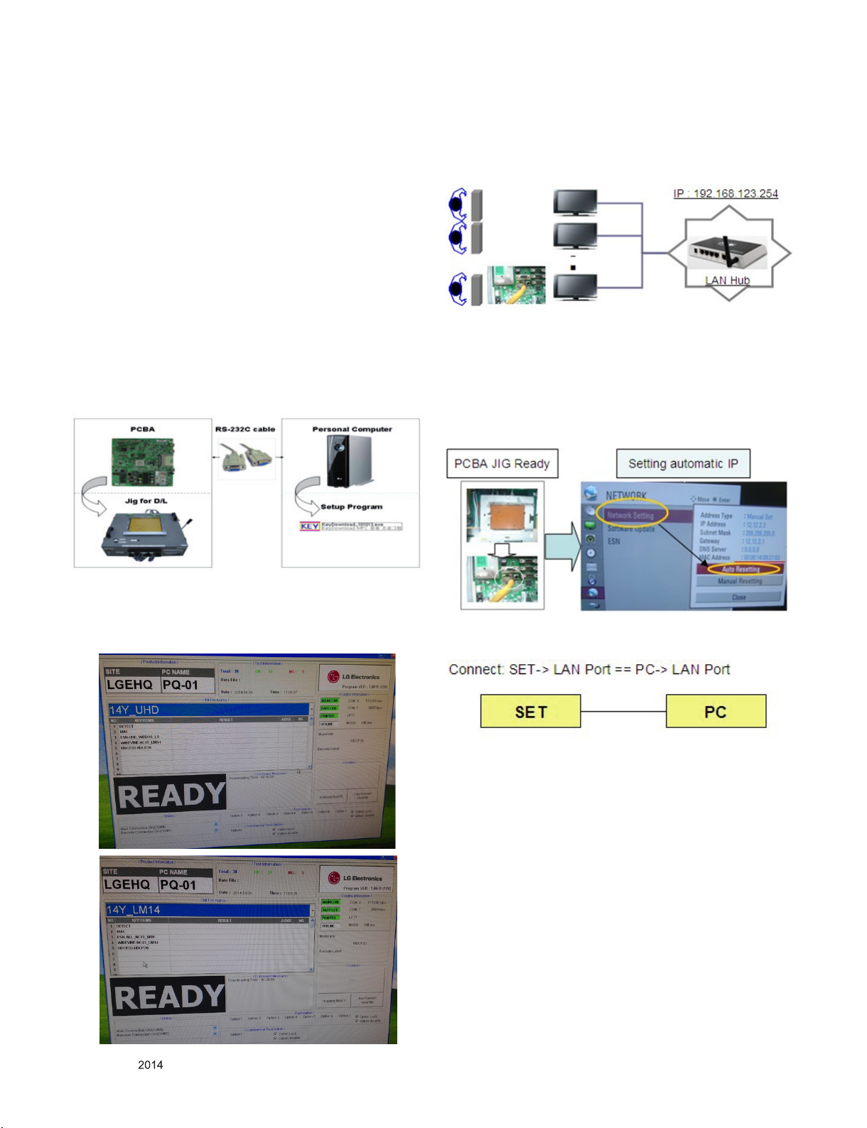
4.2.2. Communication Port connection
1) Key Write: Com 1,2,3,4 and 115200 (Baudrate)
2) Barcode: Com 1,2,3,4 and 9600 (Baudrate)
4.2.3. Download process
1) Select the download items.
2) Mode check: Online Only
3) Check the test process : DETECT -> MAC -> Widevine
4) Play: START
5) Check of result: Ready, Test, OK or NG
4.2.4. Communication Port connection
1) ) Connect: PCBA Jig -> RS-232C Port == PC -> RS-232C
Port
4.3. LAN Inspection
4.3.1. Equipment & Condition
▪ Each other connection to LAN Port of IP Hub and Jig
4.3.2. LAN inspection solution
▪ LAN Port connection with PCB
▪ Network setting at MENU Mode of TV
▪ Setting automatic IP
▪ Setting state confirmation
- If automatic setting is finished, you confirm IP and MAC
Address.
4.2.5. Download
1) TW/CO Models (14Y LCD TV + MAC + Widevine + ESN +
HDCP2.0)
4.3.3. LAN PORT INSPECTION (PING TEST)
1) Play the LAN Port Test PROGRAM.
2) Input IP set up for an inspection to Test
Program.
*IP Number : 12.12.2.2.
Only for training and service purposes
- 17 -
LGE Internal Use OnlyCopyright © LG Electronics. Inc. All rights reserved.
4.3.4. LAN PORT inspection (PING TEST)
1) Play the LAN Port Test Program.
2) connect each other LAN Port Jack.
3) Play Test (F9) button and confirm OK Message.
4) remove LAN CABLE
* Manual Download (Model Name and Serial Number)
If the TV set is downloaded By OTA or Service ma n,
sometimes model name or serial number is initialized. ( not
always)
It is impossible to download by bar code scan, so It need
Manual download.
a. Press the ‘INSTART’ key of ADJ remote controller.
b. Go to the menu ‘7. Model Number D/L’ like below photo.
c. Input the Factory model name or Serial number like below
photo.
4.4. Model name & Serial number Download
4.4.1. Model name & Serial number D/L
▪ Pr ess “Power on” key of service re mocon.(Bau d rate :
115200 bps)
▪ Connect RS-232C Signal to USB Cable to USB.
▪ Write Serial number by use USB port.
▪ Must check the serial number at Instart menu.
■ Method & Notice
A. Serial number D/L is using of scan equipment.
B. Setting of scan equipment operated by Manufacturing
Technology Group.
C. Serial number D/L must be conformed when it is produced
in production line, because serial number D/L is mandatory
by D-book 4.0
d. Check the model name INSTART menu -> Factory name
displayed
e. Check the Diagnostics (DTV country only) -> Buyer model
displayed
4.5. WIFI MAC ADDRESS CHECK
4.5.1. Using RS232 Command
Command Set ACK
Transmission [A][l][][Set ID][][20][Cr] [O][K][x] or [N][G]
■ Check the menu on in-start
Only for training and service purposes
- 18 -
LGE Internal Use OnlyCopyright © LG Electronics. Inc. All rights reserved.
5. Manual Adjustment
5.1. ADC adjustment is not needed because of
OTP (Auto ADC adjustment)
5.2. EDID
(The Extended Display Identification Data)
/ DDC (Display Data Channel) download
5.2.1. Overview
It is a VESA regulation. A PC or a MNT will display an optimal
resolution through information sharing without any necessity of
user input. It is a realization of “Plug and Play”.
5.2.2. Equipment
▪ Since embedded EDID data is used, EDID download JIG,
HDMI cable and D-sub cable are not need.
▪ Adjust remocon
5.2.3. Download method
1) Press Adj. key on the Adjust remocon, then select “12.EDID
D/L”.
By pressing Enter key, enter EDID D/L menu
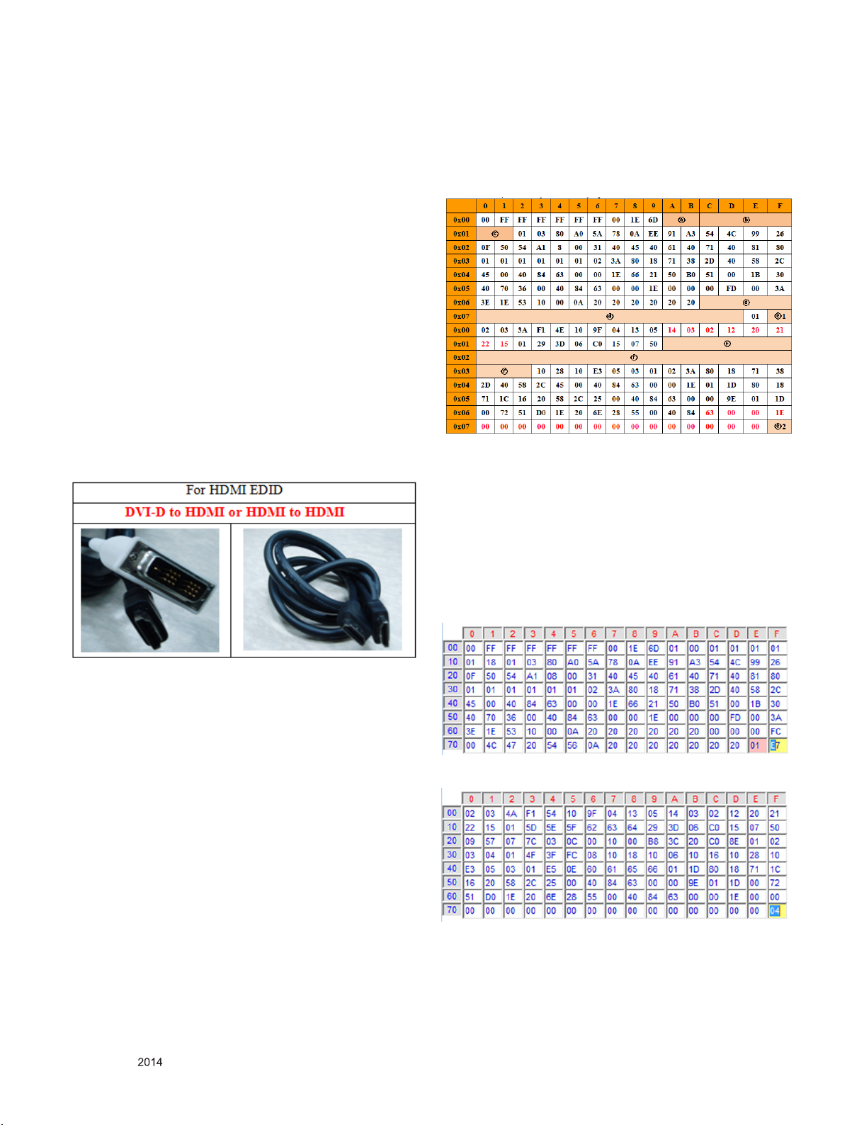
5.2.4. EDID DATA
▪ Reference
- HDMI1 ~ HDMI3
- HDMI1 ~ HDMI4
- In the data of EDID, bellows may be different by Input mode
ⓐ Product ID
ⓑ Serial No: Controlled on production line.
ⓒ Month, Year: Controlled on production line:
ex) Monthly : ‘01’ -> ‘01’
Year : ‘2014’ -> ‘18
ⓓ Model Name(Hex): LGTV
ⓔ Checksum(LG TV): Changeable by total EDID data.
ⓕ Vendor Specific(HDMI)
2) Select [Start] button by pressing Enter key, HDMI1 / HDMI2
/ HDMI3 / HDMI4 are Writing and display OK or NG.
5.2.4.1. EDID(For UB98, UB95, UB85)
# HDMI1 (C/S: 0xE7, 0x04)
EDID Block 0, Bytes 0-127
EDID Block 1, Bytes 128-255
Only for training and service purposes
- 19 -
LGE Internal Use OnlyCopyright © LG Electronics. Inc. All rights reserved.
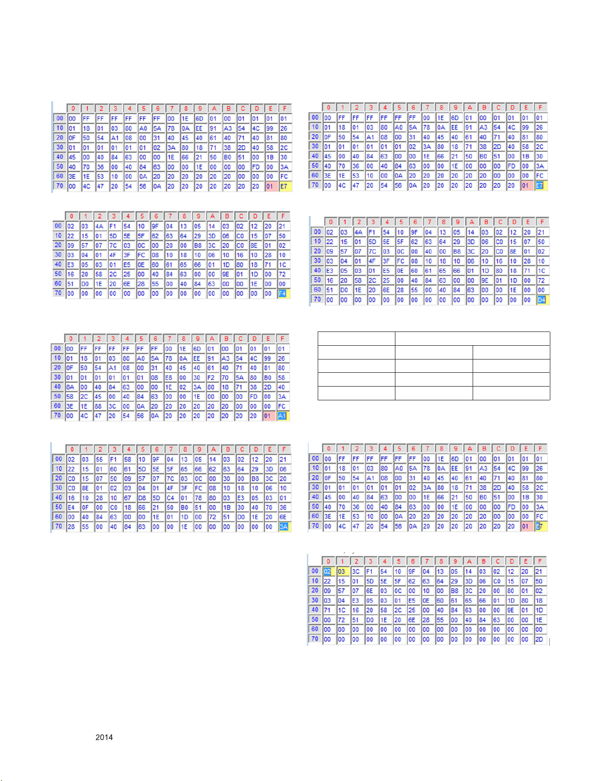
# HDMI2 (C/S: 0xE7, 0xF4)
EDID Block 0, Bytes 0-127
# HDMI4 (C/S: 0xE7, 0xD4)
EDID Block 0, Bytes 0-127
EDID Block 1, Bytes 128-255
# HDMI3 (C/S: 0xA1, 0x3A)
EDID Block 0, Bytes 0-127
EDID Block 1, Bytes 128-255
EDID Block 1, Bytes 128-255
* Checksum (HDMI 1/2/3/4)
Input FFh (Checksum)
HDMI1 E7 04
HDMI2 E7 F4
HDMI3 A1 3A
HDMI4 E7 D4
5.2.4.2. EDID(For UB93)
# HDMI1 (C/S: 0xE7, 0x2D)
EDID Block 0, Bytes 0-127
Only for training and service purposes
- 20 -
EDID Block 1, Bytes 128-255
LGE Internal Use OnlyCopyright © LG Electronics. Inc. All rights reserved.
# HDMI2 (C/S: 0xE7, 0x1D)
EDID Block 0, Bytes 0-127
# HDMI4 (C/S: 0xE7, 0xFD)
EDID Block 0, Bytes 0-127
EDID Block 1, Bytes 128-255
# HDMI3 (C/S: 0xA1, 0x63)
EDID Block 0, Bytes 0-127
EDID Block 1, Bytes 128-255
EDID Block 1, Bytes 128-255
* Checksum (HDMI 1/2/3/4)
Input FFh (Checksum)
HDMI1 E7 2D
HDMI2 E7 1D
HDMI3 A1 63
HDMI4 E7 FD
5.2.4.3. EDID(For UB83)
# HDMI 1(C/S : E7 E0)
EDID Block 0, Bytes 0-127 [00H-7FH]
Only for training and service purposes
- 21 -
EDID Block 1, Bytes 128-255 [80H-FFH]
LGE Internal Use OnlyCopyright © LG Electronics. Inc. All rights reserved.
# HDMI 2(C/S : E7 D0)
EDID Block 0, Bytes 0-127 [00H-7FH]
EDID Block 1, Bytes 128-255 [80H-FFH]
# HDMI 3(C/S : E7 C0)
EDID Block 0, Bytes 0-127 [00H-7FH]
5.3. Camera Port Inspection(For UB98, UC9)
(1) Objective : To check how it connects between Camera and
PCBA normally, and their Function
(2) Test Method : This Inspection is available only Power-Only
Status.
i) Push Camera Up
ii) Camera’s Preview picture appears on TV Set
iii) Push Camera Down
(3) RS-232C Command
RS-232C COMMAND
CMD DATA ID
Ai 00 23 Camera Function Start.
Ai 00 24 Camera Function End.
Explanation
5.4. V-COM Adjust
(*) ONLY FO R G P2 20 10 ye ar mo del. GP3 LW Se ries
[2011year] spec out !
EDID Block 1, Bytes 128-255 [80H-FFH]
* Checksum (HDMI 1/2/3)
Input FFh (Checksum)
HDMI1 E7 E0
HDMI2 E7 D0
HDMI3 E7 C0
5.5. Adjustment White balance
5.5.1. Overview
▪ W/B adj. Objective & How-it-works
(1) Objective: To reduce each Panel’s W/B deviation
(2) How-it-works: When R/G/B gain in the OSD is at 192, it
means the panel is at its Full Dynamic Range. In order to
prevent saturation of Full Dynamic range and data, one of
R/G/B is fixed at 192, and the other two is lowered to find
the desired value.
(3) Adj. condition: normal temperature
- Surrounding Temperature: 25±5 °C
- Warm-up time: About 5 Min
- Surrounding Humidity: 20% ~ 80%
5.5.2. Equipment
(1) Color Analyzer: CA-210 (LED Module : CH 14)
(2) Adj. Computer (During auto adj., RS-232C protocol is
needed)
(3) Adjust Remocon
(4) Vi deo Sig nal Generator MSP G-925F 720p/216 -Gray
(Model:217, Pattern:78)
-> Only when internal pattern is not available
※ Color Analyzer Matrix should be calibrated using CS-1000
Only for training and service purposes
- 22 -
LGE Internal Use OnlyCopyright © LG Electronics. Inc. All rights reserved.
5.5.3. Equipment connection MAP
5.5.4. Adj. Command (Protocol)
<Command Format>
START 6E A 50 A LEN A 03 A CMD A 00 A VAL A CS
A STOP
- LEN: Number of Data Byte to be sent
- CMD : Command
- VAL : FOS Data value
- CS : Checksum of sent data
- A : Acknowledge
Ex) [Send: JA_00_DD] / [Ack: A_00_okDDX]
(1) RS-232C Command used during auto-adj.
RS-232C COMMAND
CMD DATA ID
wb 00 00 Begin White Balance adj.
wb 00 10 Gain adj.(internal white pattern)
wb 00 1f Gain adj. completed
wb 00 20 Offset adj.(internal white pattern)
wb 00 2f Offset adj. completed
wb 00 ff End White Balance adj.
(internal pattern disappears )
Ex) wb 00 00 -> Begin white balance auto-adj.
wb 00 10 -> Gain adj.
ja 00 ff -> Adj. data
jb 00 c0
...
...
wb 00 1f -> Gain adj. complete
*(wb 00 20(start), wb 00 2f(endc)) -> Off-set adj.
wb 00 ff -> End white balance auto adj.
Explanation
(2) Adjustment Map
(Applied Model : LB41U Chassis ALL MODELS)
Adj. item Command
(lower caseASCII)
CMD1 CMD2 MIN MAX
Cool R Gain j g 00 C0
G Gain j h 00 C0
B Gain j i 00 C0
Medium R Gain j a 00 C0
G Gain j b 00 C0
B Gain j c 00 C0
Warm R Gain j d 00 C0
G Gain j e 00 C0
B Gain j f 00 C0
Data Range
(Hex.)
5.5.5. Adjustment method
5.5.5.1. Auto WB calibration
(1) Set TV in adj. mode using POWER ONNY key
(2) Zero calibrate probe then place it on the center of the
Display
(3) Connect Cable (RS-232C to USB)
(4) Select mode in adj. Program and begin adj.
(5) When adj. is complete (OK Sign), check adj. status pre
mode(Warm, Medium, Cool)
(6) Remove probe and RS-232C to USB cable to complete adj.
▪ W/B Adj. must begin as start command “wb 00 00” , and
finish as end command “wb 00 ff”, and Adj. offset if need
5.5.5.2. Manual adj. method
1) Set TV in Adj. mode using POWER ON
2) Zero Calibrate the probe of Color Analyzer, then place it on
the center of LCD module within 10cm of the surface..
3) Press ADJ key -> EZ adjust using adj. R/C -> 7. White-
Balance then press the cursor to the right (KEY►).
(When KEY(►) is pressed 216 Gray internal pattern will be
displayed)
4) One of R Gain / G Gain / B Gain should be fixed at 192, and
the rest will be lowered to meet the desired value.
5) Adj. is performed in COOL, MEDIUM, WARM 3 modes of
color temperature.
Only for training and service purposes
- 23 -
LGE Internal Use OnlyCopyright © LG Electronics. Inc. All rights reserved.
** R-fix adjustment
Adjust modes (Cool), Fix the R gain to 210 (default data) and
change the others (G/B Gain ).
- Adjust the R gain more than 210 ( If G gain or B gain is less
than 0 , R gain can adjust more than 210 ) and
change the others ( G/B Gain ).
Adjust two modes (Medium / Warm), Fix the one of R/G/B gain
to 192 (default data) and decrease the others.
▪ If internal pattern is not available, use RF input. In EZ Adj.
menu 7.White Balance, you can select one of 2 Test-pattern:
ON, OFF. Default is inner(ON). By selecting OFF, you can
adjust using RF signal in 216 Gray pattern.
▪ Adj. condition and cautionary items
1) Lighting condition in surrounding area
Surrounding lighting should be lower 10 lux. Try to isolate
adj. area into dark surrounding.
2) Probe location
- PDP : Color Analyzer (CA-100, CA-100+, CA210) probe
should be firmly attached to the Module
- LCD : Color Analyzer (CA-210) probe should be within 10cm
and perpendicular of the module surface (80°~ 100°)
3) Aging time
- After Aging Start, Keep the Po wer ON status during 5
Minutes.
- In case of LCD, Back-light on should be checked using no
signal or Full-white pattern.
5.5.6. Reference (White Balance Adj. coordinate and
color temperature)
▪ Luminance: 206 Gray
▪ Standard color coordinate and temperature using CS-1000
(over 26 inch)
Mode
Cool 0.271 0.270 13,000K 0.0000
Medium 0.286 0.289 9,300K -3
Warm 0.313 0.329 6,500K 0.0000
▪ Standard color coordinate and temperature using CA-210
(CH 14)
Mode
Cool 0.271±0.002 0.270±0.002 13000K 0.0000
Medium 0.286±0.002 0.289±0.002 9300K -3
Warm 0.313±0.002 0.329±0.002 6500K 0.0000
Coordinate
X Y
Coordinate
X Y
Temp △uv
Temp △uv
5.5.7. EDGE & IOL LED White balance table
▪ Edge & ALEF LED module change color coordinate because
of aging time
▪ apply under the color coordinate table, for compensated
aging time
(Normal line) Edge & ALEF LED White balance table
- gumi(Mar~Dec) & Global
Model : (normal line)LGD, CMI
webOS
Aging time
(Min)
1 0-2 282 289 297 308 324 348
2 3-5 281 287 296 306 323 346
3 6-9 279 284 294 303 321 343
4 10-19 277 280 292 299 319 339
5 20-35 275 277 290 296 317 336
6 36-49 274 274 289 293 316 333
7 50-79 273 272 288 291 315 331
8 80-119 272 271 287 290 314 330
9 Over 120 271 270 286 289 313 329
- gumi Winter table(Jan, Fab) – Gumi producing model use only
Model : (normal line) LGD
webOS
Aging time
(Min)
1 0-2 286 295 301 314 328 354
2 3-5 284 290 299 309 326 349
3 6-9 282 287 297 306 324 346
4 10-19 279 283 294 302 321 342
5 20-35 276 278 291 297 318 337
6 36-49 274 275 289 294 316 334
7 50-79 273 272 288 291 315 331
8 80-119 272 271 287 290 314 330
9 Over 120 271 270 286 289 313 329
(*) AUO, INX, Sharp, CSOT, BOE(Cool 1300K)
Cool Medium Warm
webOS
Target 278 280 293 299 320 339
x y x y x y
271 270 285 293 313 329
Cool Medium Warm
X Y X Y X Y
271 270 286 289 313 329
Cool Medium Warm
X Y X Y X Y
271 270 286 289 313 329
Only for training and service purposes
- 24 -
LGE Internal Use OnlyCopyright © LG Electronics. Inc. All rights reserved.
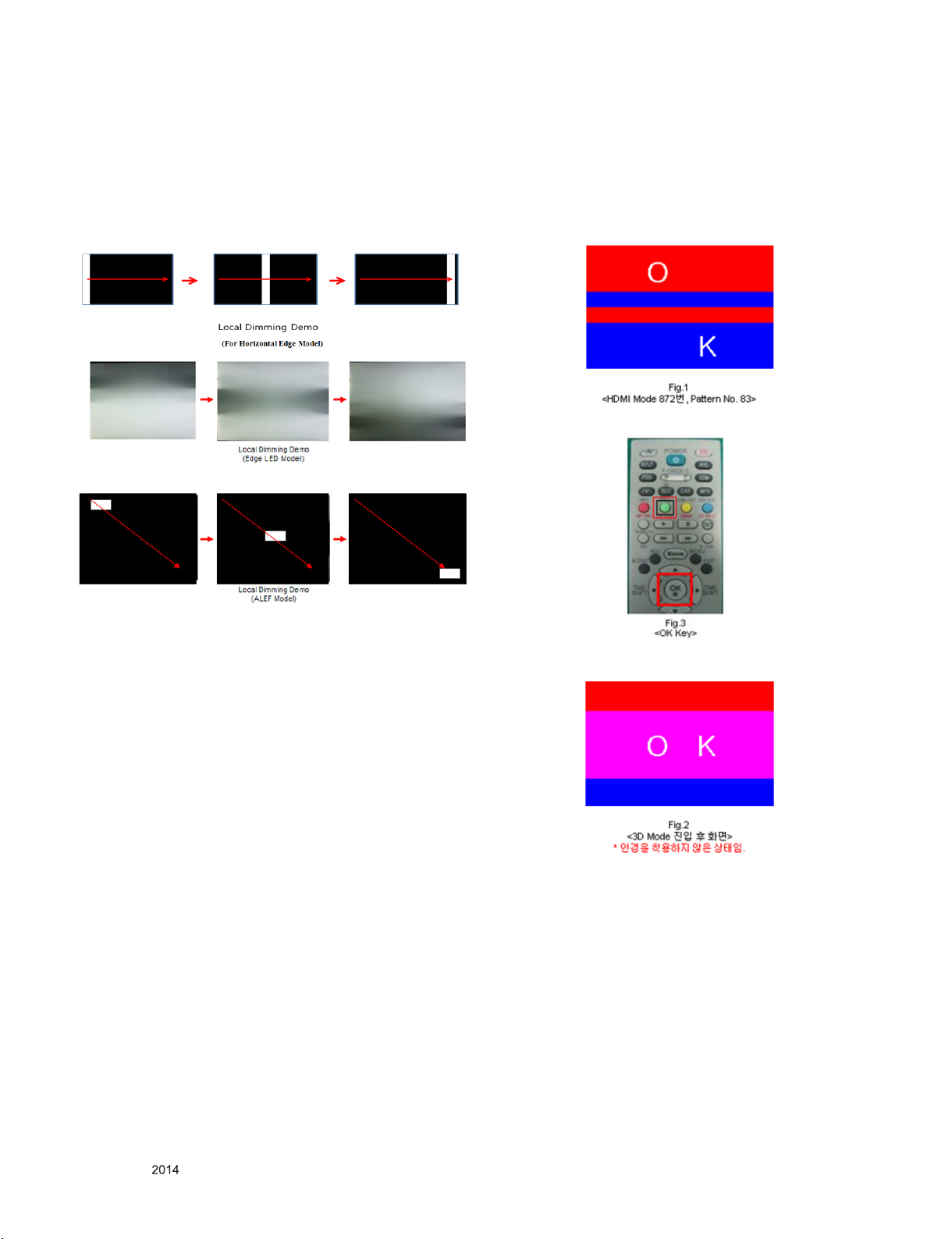
5.6. Local Dimming Function Check
Step 1) Turn on TV
Step 2) At the Local Dimming mode, module Edge Backlight
moving right to left
Back light of IOP module moving
Step 3) confirm the Local Dimming mode
Step 4) Press “exit” Key
5.8. 3D function test (Except UB93 Series)
(P at te rn Ge ne ra to r M SH G- 60 0, MS PG -6 10 0 [ SU PP ORT
HDMI1.4])
* HDMI mode NO. 872 , pattern No.83
1) Please input 3D test pattern like below (HDMI mode NO. 872 ,
pattern No.83)
2) When 3D OSD appear automatically , then select green button
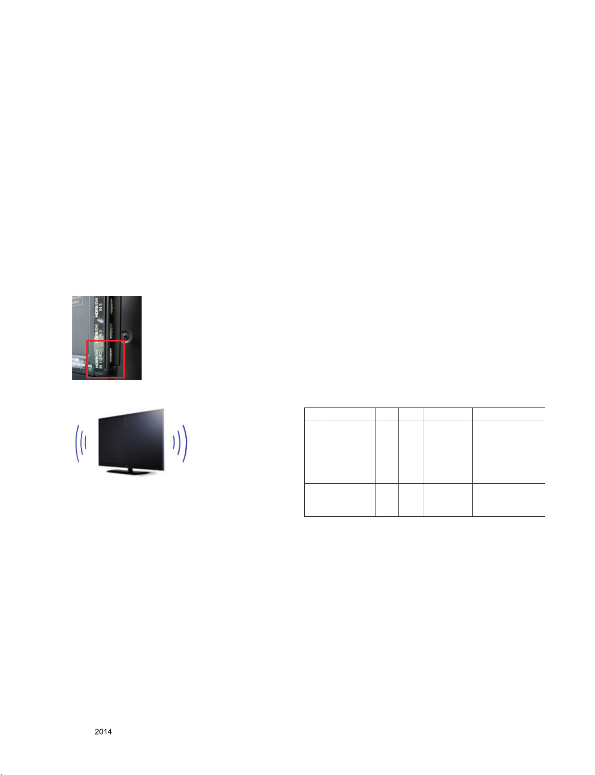
5.7. Magic Motion Remocon test
- Equipment : RF Remocon for test, IR-KEY-Code Remocon
for test
- You must confirm the battery power of RF-Remocon before
test
(recommend that change the battery per every lot)
- Sequence (test)
a) if you select the ‘start key(OK)’ on the controller, you can
pairing with the TV SET.
b) You can check the cursor on the TV Screen, when select
the ‘OK Key’ on the controller
c) You must remove the pairing with the TV Set by select
‘Mute + OK Key’ on the controller
3) Don’t wear a 3D Glasses, Check the picture like below
Only for training and service purposes
- 25 -
LGE Internal Use OnlyCopyright © LG Electronics. Inc. All rights reserved.
5.9. Option selection per country
5.9.1. Overview
▪ Option selection is only done for models in AJ/JA/IL
5.9.2. Method
1) Press ADJ key on the Adj. R/C, then select Country Group
Meun
2) Depending on destination, select Country Group Code or
Country Group then on the lower Country option, select US,
CA, MX. Selection is done using +, - or ►◄ KEY
5.10. HDMI ARC Function Inspection
5.10.1. Test equipment
- Optic Receiver Speaker
- MSHG-600 (SW: 1220 ↑)
- HDMI Cable (for 1.4 version)
5.10.2. Test method
(1) Insert the HDMI Cable to the HDMI ARC port from the
master equipment (HDMI1)
7. GND and Internal Pressure check
7.1. Method
1) GND & Internal Pressure auto-check preparation
- Check that Power Cord is fully inserted to the SET. (If loose,
re-insert)
2) Perform GND & Internal Pressure auto-check
- Unit fully inserted Power cord, Antenna cable and A/V arrive
to the auto-check process.
- Connect D-terminal to AV JACK TESTER
- Auto CONTROLLER(GWS103-4) ON
- Perform GND TEST
- If NG, Buzzer will sound to inform the operator.
- If OK, changeover to I/P check automatically.
(Remove CORD, A/V form AV JACK BOX)
- Perform I/P test
- If NG, Buzzer will sound to inform the operator.
- If OK, Good lamp will lit up and the stopper will allow the
pallet to move on to next process.
7.2. Checkpoint
(1) Test voltage
- GND: 1.5KV/min at 100mA
- SIGNAL: 3KV/min at 100mA
(2) TEST time: 1 second
(3) TEST POINT
- GND Test = POWER CORD GND and SIGNAL CABLE GND.
- Hi-pot Test = POWER CORD GND and LIVE & NEUTRAL.
(4) LEAKAGE CURRENT: At 0.5mArms
(2) Check the sound from the TV Set
(3) Check the Sound from the Speaker or using AV & Optic
TEST program (It’s connected to MSHG-600)
8. AUDIO output check
No Item Min Typ Max Unit Remark
1 Audio practi-
cal max
Output, L/R
(Distortion=10%
max Output)
2
Speaker
(8Ω Impedance)
*Measurement condition:
(1) RF input: Mono, 1KHz sine wave signal, 100% Modulation
(2) CVBS, Component: 1KHz sine wave signal (0.4Vrms)
(3) RGB PC: 1KHz sine wave signal (0.7Vrms)
10.0
12.0
8.10
10.8WVrms
10 12 W EQ On
EQ Off
AVL Off
Clear Voice Off
AVL On
Clear Voice On
Only for training and service purposes
- 26 -
LGE Internal Use OnlyCopyright © LG Electronics. Inc. All rights reserved.
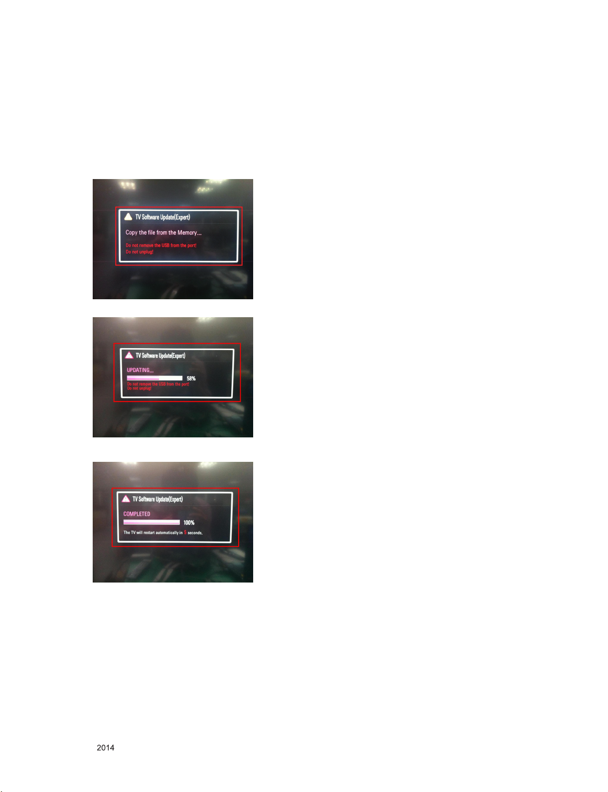
9. USB S/W Download
(optional, Service only)
(1) Put the USB Stick to the USB socket
(2) Automatically detecting update file in USB Stick
- If your downloaded program version in USB Stick is lower
than that of TV set, it didn’t work. Otherwise USB data is
automatically detected.
(3) Show the message “Copying files from memory”
(4) Updating is staring
(5) Updating Completed, The TV will restart automatically
(6) If your TV is turned on, check your updated version and
Tool option.
* If downloading version is more high than your TV have, TV
can lost all channel data. In this case, you have to channel
recover. If all channel data is cleared, you didn’t have a DTV/
ATV test on production line.
* After downloading, TOOL OPTION setting is needed again.
(1) Push "IN-START" key in service remote controller.
(2) Select "Tool Option 1" and Push “OK” button.
(3) Punch in the number. (Each model has their number.)
Only for training and service purposes
- 27 -
LGE Internal Use OnlyCopyright © LG Electronics. Inc. All rights reserved.
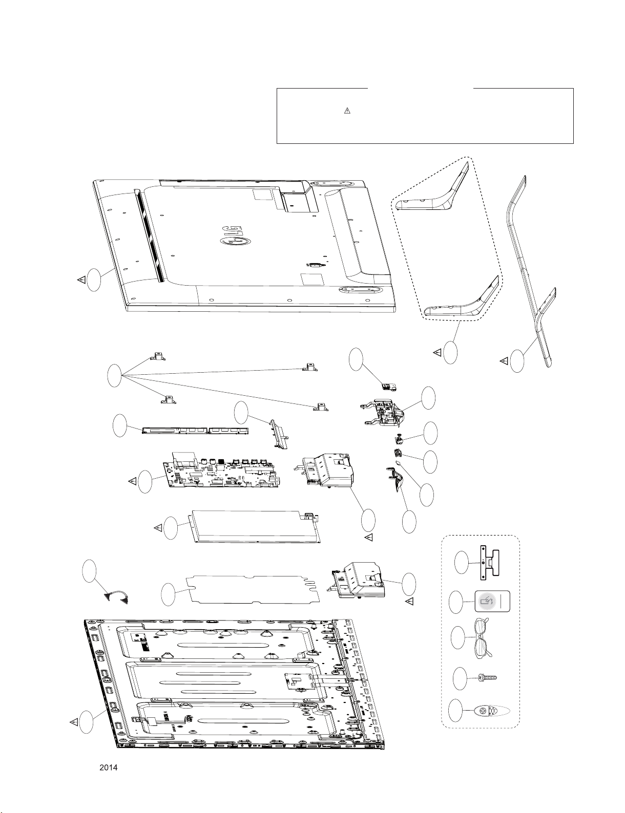
EXPLODED VIEW
IMPORTANT SAFETY NOTICE
Many electrical and mechanical parts in this chassis have special safety-related characteristics. These
parts are identified by in the Schematic Diagram and EXPLODED VIEW.
It is essenti al that these special safet y parts shoul d be replac ed with the same compo nents as
recommended in this manual to prevent X-RADIATION, Shock, Fire, or other Hazards.
Do not modify the original design without permission of manufacturer.
400
570
910
900
410
503
522
521
500
501
540
504
530
121
LV1
502
CAM1
120
820
AT1
AG1
200
Only for training and service purposes
- 28 -
A10
Set + Stand
A22
LGE Internal Use OnlyCopyright © LG Electronics. Inc. All rights reserved.
System Configuration
Copyright ⓒ 2014 LG Electronics. Inc. All right reserved.
Only for training and service purposes
LGE Internal Use Only
Clock for LG1154D
MAIN Clock(24Mhz)
8pF
C100
8pF
C101
System Clock for Analog block(24Mhz)
OPT
R100 33
R101 33
OPT
T32
0.1uF
P100
12505WS-10A00
T32
1
2
3
4
5
6
7
8
9
10
11
WebOS UHD HW Option
BIT0
BIT1
BIT2
BIT3
BIT4
BIT5
BIT6
BIT7
BIT8
BIT9
BIT10
20131016 version
00
01
10
11
00
01
10
11
DVB
TW/COL
CN/HK
EU
AJJA
Resolution
Support U14
D9 Model
URSA7/URSA9
EU/CIS
T/C
T2/C/S2/ATV_EXT
T2/C
T2/C/S2/AT
Display
Reserved
BIT(0/1)
BIT2
BIT3
BIT4
BIT(6/7)
BIT8
BIT9
BIT10 Reserved
X-TAL_1
GND_1
1
2
4
3
GND_2
X-TAL_2
PLLSET1
PLLSET0
+3.3V_NORMAL
OPT
R160 10K
ATSC
North.AM.
KR
BR
High
FHD
U14
D9
URSA9
AJJA
T/C
T2/C_PIP
T2/C
T2/C/S2
High
OLED
XIN_MAIN
1M
R108
X100
24MHz
XO_MAIN
PLL SET[1:0] : internal pull up
"00" : CPU(1200Mhz),M0 / M1 DDR(792,792 Mhz)
"01" : CPU(1056Mhz),M0 / M1 DDR(672,672 Mhz)
"10" : CPU(1056Mhz),M0 / M1 DDR(792,792 Mhz)
"11" : CPU( 960Mhz),M0 / M1 DDR(792,792 Mhz)
Jtag I/F
For Main
OPT
R167
33
TRST_N0
TDI0
TDO0
TMS0
TCK0
SOC_RESET
OPT
OPT
OPT
R163 10K
R166 10K
R168 10K
+3.3V_NORMAL
URSA7/URSA9PBIT5
BIT0_1
R110 10K
BIT0_0
R109 10K
JP
JP
Low
UHD
Non_U14
Non_D9
T2/C_PIP
Low
LCD
TW/COL
T/C
T2/C
10K
BIT1_1
R112
10K
BIT1_0
R111
FHD
UHD
R114 10K
R113 10K
CN/HK
Default
U14
R116 10K
NON_U14
R115 10K
D9
NOT_D9
ATSC_PIP
ATV_SOC
ATV_EXT
R120 10K
R119 10K
KR
URSA9
BIT6_1
R124 10K
R122 10K
BIT6_0
R123 10K
R121 10K
URSA7/URSA9P
North.AM
ATSC_PIP
ATV_SOC
ATV_EXT
OP MODE[1:0]
"00" : Normal Mode
"01/10/11" : Internal Test mode
+3.3V_NORMAL
OLED
BIT7_1
R126 10K
R128 10K
R129 10K
OPT
LCD
BIT7_0
R130 10K
R127 10K
R125 10K
BR
ISDB_PIP
ISDB
NVRAM
EEPROM_RENESAS
IC102
R1EX24256BSAS0A
A0
1
A1
2
A2
A0’h
3
VSS
4
OPT
R133 33
R134 33
OPT
R131 10K
OPT
R132 10K
JP
Default
VCC
8
WP
7
SCL
6
SDA
5
OPM1
OPM0
+3.3V_LNA_TU
C103
0.1uF
D13_INT
EPHY_INT
R135
1.8K
KR_PIP_NOT
1.5K
KR_PIP
R135-*1
+3.3V_NORMAL
Write Protection
- Low : Normal Operation
- High : Write Protection
AR102
+3.3V_NORMAL
OPT
INSTANT_MODE0
+3.3V_NORMAL
R137
1.8K
R136
1.8K
R138
1.8K
KR_PIP_NOT
1.5K
KR_PIP
R136-*1
33
INSTANT boot MODE
"1 : Instant boot
"0 : normal
3.3K
R150
(internal pull down)
R164331/16W
5%
+3.3V_TUNER
R142
1.8K
R141
1.8K
I2C_SCL5
I2C_SDA5
INSTANT_BOOT
SOC_RESET
R149
10K
H13_CONNECT
+3.3V_NORMAL
R144
1.8K
R143
1.8K
EEPROM_ST
M24256-BRMN6TP
E0
1
E1
2
E2
3
VSS
4
EEPROM_ATMEL
AT24C256C-SSHL-T
A0
1
A1
2
A2
3
GND
4
BOOT_MODE0
R151
I2C_SCL_MICOM_SOC
I2C_SDA_MICOM_SOC
I2C PULL UP
R146
1.8K
R147
1.8K
R145
1.8K
I2C_CH1_pullup_1.8K
IC102-*1
VCC
8
WC
7
SCL
6
SDA
5
IC102-*2
VCC
8
WP
7
SCL
6
SDA
5
+3.3V_NORMAL
BOOT MODE
"0 : EMMC
"1 : TEST MODE
3.3K
R117
OPT
3.3K
R118
XIN_MAIN
XO_MAIN
C108
0.1uF
H13A_SCL
H13A_SDA
TRST_N0
PLLSET1
PLLSET0
BOOT_MODE
CAM_TRIGGER_DET
SOC_RX
10K
SOC_TX
M_REMOTE_RX
M_REMOTE_TX
M_REMOTE_RTS
M_REMOTE_CTS
SOC_SPI1_CS
SOC_SPI1_MOSI
SOC_SPI1_MISO
U14 SPI
SOC_SPI1_SCLK
SOC_SPI0_CS0
SOC_SPI0_MOSI
SOC_SPI0_MISO
D13 SPI
SOC_SPI0_SCLK
I2C_SCL1
I2C_SDA1
I2C_SCL2_SOC
I2C_SDA2_SOC
I2C_SCL4
I2C_SDA4
I2C_SCL5
I2C_SDA5
I2C_SCL6
I2C_SDA6
I2C_SDA_MICOM
I2C_SCL_MICOM
I2C_SDA2
I2C_SCL2
I2C_CH1_pullup_1.8K
R148
1.8K
I2C_SDA1
I2C_SCL1
I2C_SDA_MICOM_SOC
I2C_SCL_MICOM_SOC
I2C_SDA2_SOC
I2C_SCL2_SOC
I2C_SDA4
I2C_SCL4
I2C_SDA5
I2C_SCL5
I2C_SDA6
I2C_SCL6
OPM1
TMS0
TCK0
TDI0
TDO0
BOOT_MODE
H13D_XTAL_560ohm
H13D_XTAL_100ohm
R152-*1
AR100
0
I2C for tuner
I2C for tuner
560
R152
100
33
R1020
R104
I2C_CH1_pullup_3.3K
I2C_CH1_pullup_3.3K
I2C_SDA_MICOM_SOC
I2C_SCL_MICOM_SOC
I2C_SDA2_SOC
I2C_SCL2_SOC
R147-*1
3.3K
R148-*1
3.3K
A26
XIN
B26
XOUT
B27
XTAL_BYPASS
AT37
H13DA_XTAL
AU16
PORES_N
AD34
OPM1
AD33
OPM0
AT26
H13DA_SCL
AU26
H13DA_SDA
AP9
TRST_N0
AN9
TMS0
AP11
TCK0
AN11
TDI0
AN10
TDO0
AM10
TRST_N1
AM9
TMS1
AM11
TCK1
AM12
TDI1
AL11
TDO1
AL9
PLLSET1
AL10
PLLSET0
AE34
BOOT_MODE
Y33
EXT_INTR3/GPIO70
W32
EXT_INTR2/GPIO69
W33
EXT_INTR1/GPIO68
W34
EXT_INTR0/GPIO67
AU12
UART0_RXD
AT12
UART0_TXD
AU13
UART1_RXD
AT13
UART1_TXD
AP12
UART1_RTS
AR12
UART1_CTS
AE35
SPI_CS0/GPIO36
AE36
SPI_DO0/GPIO38
AF36
SPI_DI0/GPIO39
AF35
SPI_SCLK0/GPIO37
AG34
SPI_CS1
AF33
SPI_DO1
AG33
SPI_DI1
AG32
SPI_SCLK1
AR15
SCL0/GPIO66
AP15
SDA0/GPIO65
AR16
SCL1/GPIO64
AP16
SDA1/GPIO79
AP17
SCL2/GPIO78
AR17
SDA2/GPIO77
AP6
SCL3
AR6
SDA3
AH32
SCL4
AJ33
SDA4
AH34
SCL5
AH33
SDA5
+3.3V_NORMAL
CAM_CE1_N
CAM_CE2_N
CAM_CD1_N/GPIO76
F33
F34
D32
E32
/PCM_CE1
/PCM_CE2
CAM_CD1_N
CI
USB_CTL3
/USB_OCD3
/USB_OCD2
USB_CTL2
K35
K36
K37
L35
EB_CS3/GPIO93
EB_CS2/GPIO92
EB_CS1/GPIO91
EB_CS0/GPIO90
EB_BE_N1
EB_WE_N
EB_OE_N
H35
H36
J35
J36
H37
EB_WE_N/GPIO95
EB_WAIT/GPIO94
EB_OE_N/GPIO82
EB_BE_N1/GPIO81
EB_ADDR[0-14]
EB_BE_N0
EB_ADDR[14]
EB_ADDR[13]
EB_ADDR[12]
G37
G36
G35
F36
EB_BE_N0/GPIO80
EB_ADDR15/GPIO89
EB_ADDR14/GPIO88
EB_ADDR13/GPIO103
EB_ADDR12/GPIO102
EB_ADDR[6]
EB_ADDR[9]
EB_ADDR[8]
EB_ADDR[7]
EB_ADDR[10]
EB_ADDR[11]
F35
E36
E37
E35
D37
EB_ADDR9/GPIO99
EB_ADDR8/GPIO98
EB_ADDR7/GPIO97
EB_ADDR11/GPIO101
EB_ADDR10/GPIO100
EB_ADDR[3]
EB_ADDR[4]
EB_ADDR[5]
D36
D35
C36
C35
EB_ADDR6/GPIO96
EB_ADDR5/GPIO111
EB_ADDR4/GPIO110
EB_DATA[0-7]
EB_ADDR[2]
EB_ADDR[0]
EB_DATA[6]
EB_DATA[7]
EB_ADDR[1]
B37
B36
B35
C32
B33
EB_ADDR3/GPIO109
EB_ADDR2/GPIO108
EB_ADDR1/GPIO107
EB_ADDR0/GPIO106
EB_DATA7/GPIO105
EB_DATA[5]
A33
EB_DATA6/GPIO104
EB_DATA5/GPIO119
IC100
LG1154D_H13D
CAM_CD2_N/GPIO75
CAM_VS1_N/GPIO86
CAM_VS2_N/GPIO85
CAM_IREQ_N/GPIO73
CAM_RESET
CAM_INPACK/GPIO74
CAM_VCCEN_N/GPIO87
CAM_WAIT_N/GPIO84
CAM_REG_N/GPIO72
CAM_IOIS16_N/GPIO83
SC_CLK/GPIO130
SC_DETECT/GPIO133
SC_VCCEN/GPIO129
SC_VCC_SEL/GPIO128
SC_RST/GPIO131
SC_DATA/GPIO132
SD_CLK/GPIO125
SD_CMD/GPIO124
SD_CD_N/GPIO123
SD_WP_N/GPIO122
SD_DATA3/GPIO121
SD_DATA2/GPIO120
SD_DATA1/GPIO135
SD_DATA0/GPIO134
USB2_2_DP0
USB2_2_DM0
USB2_2_TXRTUNE
G32
G33
F32
G34
D33
H32
E33
D34
H33
T33
U33
T32
V32
V33
V34
A25
C25
B25
E25
D25
E24
D24
C24
L37
L36
K34
1%
200
R157
CAMERA_DP
CAM_CD2_N
R153
10K
PCM_RESET
CAM_IREQ_N
CI
R154
10K
CAM_REG_N
CAM_WAIT_N
PCM_5V_CTL
R155
10K
CI
SMARTCARD_CLK/SD_EMMC_DATA[0]
SMARTCARD_DET/SD_EMMC_DATA[3]
interface
Only SMART CARD
SMARTCARD_PWR_SEL/SD_EMMC_DATA[1]
SMARTCARD_VCC/SD_EMMC_CMD
SMARTCARD_DATA/SD_EMMC_CLK
SMARTCARD_RST/SD_EMMC_DATA[2]
CAMERA_DM
EB_DATA[0]
EB_DATA[2]
EB_DATA[1]
EB_DATA[3]
EB_DATA[4]
C33
A34
B34
C34
A36
EB_DATA4/GPIO118
EB_DATA3/GPIO117
EB_DATA2/GPIO116
EB_DATA1/GPIO115
USB2_1_DP0
USB2_1_DM0
USB2_1_TXRTUNE
M37
M36
K33
AU7
1%
200
HUB_DP
HUB_DM
R159
EMMC_DATA[0-7]
EMMC_CMD
EMMC_CLK
EMMC_RST
EMMC_DATA[7]
Y37
Y36
W35
T36
W36
EMMC_CLK
EMMC_CMD
EMMC_DATA7
EMMC_RESETN
EB_DATA0/GPIO114
USB2_0_DP
USB2_0_DM
USB2_0_TXRTUNE
USB3_DP0
USB3_DM0
AT7
AP7
P37
P36
N36
WIFI_DM
WIFI_DP
R161 200 1%
USB3_DM
USB3_DP
EMMC_DATA[3]
EMMC_DATA[4]
EMMC_DATA[6]
EMMC_DATA[5]
V35
V37
V36
U35
EMMC_DATA6
EMMC_DATA5
EMMC_DATA4
EMMC_DATA3
USB3_RX0P
USB3_RX0M
USB3_TX0P
USB3_TX0M
N37
R36
R37
N34
1%
200
R162
C105 0.1uF
C104 0.1uF
USB3_TX0P
USB3_RX0P
USB3_RX0M
USB3_TX0M
EPHY_MDIO
EPHY_REFCLK
EPHY_CRS_DV
EMMC_DATA[1]
EMMC_DATA[2]
EMMC_DATA[0]
U36
U37
AU11
AU8
AT8
EMMC_DATA2
USB3_RESREF
P33
RMII_MDIO
EMMC_DATA1
EMMC_DATA0
RMII_CRS_DV
RMII_REF_CLK
USB3_REFPADCLKM
USB3_REFPADCLKP
NC_1
NC_2
NC_3
P32
L32
L33
M31
AC-coupling CAP
Place near by LG1154D
EPHY_MDC
AR8
AR10
RMII_MDC
NC_4
AJ31
EPHY_EN
AT10
RMII_TXEN
J32
EPHY_TXD1
EPHY_RXD0
EPHY_TXD0
EPHY_RXD1
AU10
AT11
AR11
RMII_TXD1
RMII_TXD0
RMII_RXD1
RMII_RXD0
GPIO23/UART2_TX
GPIO22/UART2_RX
PHY0_ARC_OUT_0
HUB_PORT_OVER0
HUB_VBUS_CTRL0
GPIO136
GPIO137
GPIO138
GPIO139
J33
K32
J34
DPC_CTL
SIL9617_INT
R9531_RESET
R9531_FLASH_WP
GPIO31
GPIO30
GPIO29
GPIO28
GPIO27
GPIO26
GPIO25
GPIO24
GPIO21
GPIO20
GPIO19
GPIO18
GPIO17
GPIO16
GPIO15
GPIO14
GPIO13
GPIO12
GPIO11
GPIO10
GPIO9
GPIO8
GPIO7
GPIO6
GPIO5
GPIO4
GPIO3
GPIO2
GPIO1
GPIO0
DDCD0_CK
DDCD0_DA
HPD0
PHY0_RX0N_0
PHY0_RX0P_0
PHY0_RX1N_0
PHY0_RX1P_0
PHY0_RX2N_0
PHY0_RX2P_0
PHY0_RXCN_0
PHY0_RXCP_0
AL34
AM33
AM32
AF30
AN34
AK34
AL33
AL32
AR9
AM5
AM6
AM7
AL6
AK7
AK6
AK5
AJ5
AJ6
AJ7
AH6
AG7
AG6
AG5
AF5
AH30
AG30
AN33
AK33
AE30
AD30
AN32
AK32
AC32
AC33
AB33
AE37
AC36
AC37
AB36
AB37
AA36
AA37
AD36
AD37
R32
R33
RF_SWITCH_CTL
R107 100
CAM_SLIDE_DET
Compensation_Done
/RST_PHY
HDMI_HPD_3
HDMI_HPD_2
For connecting
SIC debug tool
INSTANT_BOOTOPM0
SC_DET
AV1_CVBS_DET
AMP_RESET_N
COMP1_DET
M_RFModule_RESET
HP_DET
SIL9617_RESET
/TU_RESET1
U14_RESET
D14_HWRESET
FRC_FLASH_WP
/RST_HUB
/TU_RESET2
MN864778_RESET
AMP_RESET_N_1
AR101
3.3K
SPDIF_OUT_ARC
HDMI_RX0-
HDMI_RX0+
HDMI_RX1-
HDMI_RX1+
HDMI_RX2HDMI_RX2+
HDMI_CLK-
HDMI_CLK+
/USB_OCD1
USB_CTL1
+3.3V_NORMAL
R175
3.3K
HDMI_MUX_SEL
To surround amp
AUD_LRCH2
local dimming
I2C port
+3.3V_NORMAL
Not Used Net (UB85/95/UC89)
CAM_TRIGGER_DET
H13_CONNECT
SOC_SPI1_CS
SOC_SPI1_MOSI
SOC_SPI1_MISO
SOC_SPI1_SCLK
CAM_SLIDE_DET
AUD_LRCH2
AMP_RESET_N_1
U14_RESET
/RST_HUB
AMP_RESET_N_1
M_REMOTE_RX
M_REMOTE_TX
M_REMOTE_RTS
M_REMOTE_CTS
Not Used Net (Only OLED)
DPC_CTL
Not Used Net (Only OLED 77EC98)
AMP_RESET_N
+3.3V_NORMAL
For ISP
R103
3.3K
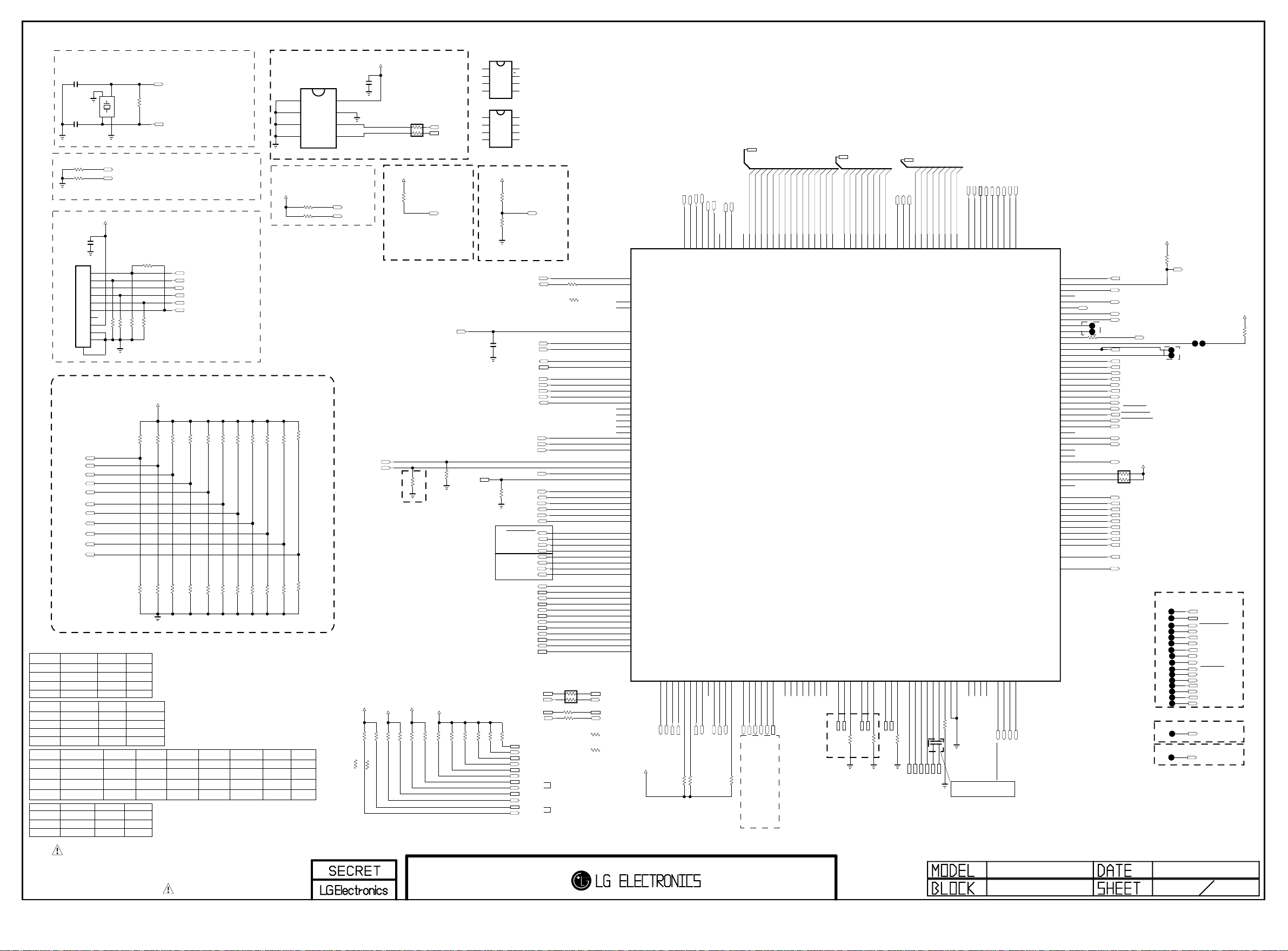
THE SYMBOL MARK OF THIS SCHEMETIC DIAGRAM INCORPORATES
SPECIAL FEATURES IMPORTANT FOR PROTECTION FROM X-RADIATION.
FIRE AND ELECTRICAL SHOCK HAZARDS, WHEN SERVICING IF IS
ESSENTIAL THAT ONLY MANUFACTURES SPECIFIED PARTS BE USED FOR
THE CRITICAL COMPONENTS IN THE SYMBOL MARK OF THE SCHEMETIC.
BSD-14Y-UD-001-HD
2013-12-17
H13 D CHIP
LG1154A
Copyright ⓒ 2014 LG Electronics. Inc. All right reserved.
Only for training and service purposes
LGE Internal Use Only
LG1154D
AVDD25
VDD25_LTX
VDDC10
AVDD33_CVBS
VDD25_REF
VDD25_LTX
VDD25_AUD
VDD10_XTAL
VDD10_XTAL
AVDD33_XTAL
VSS25_REF
LG1154A
H13A_NON_BRAZIL
E11
F5
F6
F11
G5
H13
J13
P12
P13
R5
R6
N16
T13
T14
N10
N11
N12
N13
U5
N7
N8
N9
F14
M6
N6
M13
F15
F16
H15
J15
J16
K15
K16
R18
G7
G8
G9
H7
H12
J7
J12
K7
K12
L7
L12
M7
M12
T17
T18
M8
G10
G11
G12
V5
C3
D3
D4
D17
E4
F4
F7
F8
F9
F10
F12
F13
F17
F18
G4
G6
G13
G14
G15
G16
G17
G18
H4
H5
H6
H8
H9
H10
H11
VDD33_1
VDD33_2
VDD33_3
VDD33_4
VDD33_5
VDD33_6
VDD33_7
VDD33_8
VDD33_9
VDD33_10
VDD33_11
VDD33_XTAL
AVDD33_CVBS_1
AVDD33_CVBS_2
VDD25_CVBS_1
VDD25_CVBS_2
VDD25_VSB_1
VDD25_VSB_2
VDD25_REF
VDD25_COMP_1
VDD25_COMP_2
VDD25_COMP_3
VDD25_APLL
VDD25_AUD_1
VDD25_AUD_2
VDD25_AAD
LTX_LVDD_1
LTX_LVDD_2
SDRAM_VDDQ_1
SDRAM_VDDQ_2
SDRAM_VDDQ_3
SDRAM_VDDQ_4
SDRAM_VDDQ_5
VDD10_XTAL
VDDC10_1
VDDC10_2
VDDC10_3
VDDC10_4
VDDC10_5
VDDC10_6
VDDC10_7
VDDC10_8
VDDC10_9
VDDC10_10
VDDC10_11
VDDC10_12
VDDC10_13
AVDD10_CVBS
AVDD10_VSB
AVDD10_LLPLL
DVDD10_APLL_1
DVDD10_APLL_2
LTX_VDD
VSS25_REF
GND_1
GND_2
GND_3
GND_4
GND_5
GND_6
GND_7
GND_8
GND_9
GND_10
GND_11
GND_12
GND_13
GND_14
GND_15
GND_16
GND_17
GND_18
GND_19
GND_20
GND_21
GND_22
GND_23
GND_24
GND_25
GND_26
GND_27
GND_28
GND_29
LG1154AN_H13A
AVDD33
IC101
GND_30
GND_31
GND_32
GND_33
GND_34
GND_35
GND_36
GND_37
GND_38
GND_39
GND_40
GND_41
GND_42
GND_43
GND_44
GND_45
GND_46
GND_47
GND_48
GND_49
GND_50
GND_51
GND_52
GND_53
GND_54
GND_55
GND_56
GND_57
GND_58
GND_59
GND_60
GND_61
GND_62
GND_63
GND_64
GND_65
GND_66
GND_67
GND_68
GND_69
GND_70
GND_71
GND_72
GND_73
GND_74
GND_75
GND_76
GND_77
GND_78
GND_79
GND_80
GND_81
GND_82
GND_83
GND_84
GND_85
GND_86
GND_87
GND_88
GND_89
GND_90
GND_91
GND_92
GND_93
GND_94
GND_95
GND_96
GND_97
GND_98
GND_99
GND_100
GND_101
GND_102
GND_103
GND_104
GND_105
GND_106
GND_107
GND_108
GND_109
GND_110
GND_111
GND_112
GND_113
GND_114
GND_115
GND_116
IC100
LG1154D_H13D
A24
M0_DDR_VREF1
A4
M0_DDR_VREF2
A2
M1_DDR_VREF1
Y1
M1_DDR_VREF2
P26
XTAL_VDD
N26
XTAL_VDDP
M21
VDD33_1
Y30
VDD33_2
AA30
VDD33_3
AE8
VDD33_4
AF8
VDD33_5
AK13
VDD33_6
AK24
VDD33_7
AK25
VDD33_8
M22
AVDD33_USB_1
M23
AVDD33_USB_2
AK11
AVDD33_BT_USB_1
AK12
AVDD33_BT_USB_2
AF25
AVDD33_HDMI_1
AF26
AVDD33_HDMI_2
R31
SP_VQPS
AE23
VDD25_LVRX_1
AF23
VDD25_LVRX_2
AE14
VTXPHY_VDD25_1
AF14
VTXPHY_VDD25_2
N25
VDD25_DR3PLL
AD26
GPLL_AVDD25
H10
VDD15_M0_1
H11
VDD15_M0_2
H12
VDD15_M0_3
H13
VDD15_M0_4
H14
VDD15_M0_5
H15
VDD15_M0_6
H16
VDD15_M0_7
H17
VDD15_M0_8
H18
VDD15_M0_9
H19
VDD15_M0_10
H20
VDD15_M0_11
H21
VDD15_M0_12
H22
VDD15_M0_13
H23
VDD15_M0_14
H24
VDD15_M0_15
H25
VDD15_M0_16
H7
VDD15_M1_1
H8
VDD15_M1_2
J8
VDD15_M1_3
K8
VDD15_M1_4
L7
VDD15_M1_5
L8
VDD15_M1_6
M8
VDD15_M1_7
N7
VDD15_M1_8
N8
VDD15_M1_9
P8
VDD15_M1_10
R7
VDD15_M1_11
R8
VDD15_M1_12
T8
VDD15_M1_13
U8
VDD15_M1_14
V8
VDD15_M1_15
W8
VDD15_M1_16
LG1154AN_H13A_ISDB-T (LG1154AN-IT)
P17
P18
J17
N18
D18
M18
M17
U13
V14
V15
V13
U15
U14
U10
V12
V10
U11
V11
U12
E3
K3
K2
A8
B8
U7
V6
V7
T5
T6
U8
V8
V9
U9
H13A_BRAZIL
XIN_SUB
XO_SUB
VSB_AUX_XIN
XTAL_BYPASS
CLK_24M
XTAL_SEL0
XTAL_SEL1
PORES_N
OPM0
OPM1
H13A_SCL
H13A_SDA
CVBS_IN3
CVBS_IN2
CVBS_IN1
CVBS_VCM
BUF_OUT1
BUF_OUT2
REFT
REFB
ADC1_COM
ADC2_COM
ADC3_COM
SC1_SID
SC1_FB
PB1_IN
Y1_IN
SOY1_IN
PR1_IN
PB2_IN
Y2_IN
SOY2_IN
PR2_IN
VTXPHY_VDD11_1
VTXPHY_VDD11_2
VTXPHY_VDD11_3
AVDD11_DR3PLL
IC101-*1
AAD_ADC_SIF
AAD_ADC_SIFM
AUDA_VBG_EXT
AUDA_OUTL
AUDA_OUTR
AUD_SCART_OUTL
AUD_SCART_OUTR
AUAD_L_CH4_IN
AUAD_R_CH4_IN
AUAD_L_CH3_IN
AUAD_R_CH3_IN
AUAD_L_CH2_IN
AUAD_R_CH2_IN
AUAD_L_CH1_IN
AUAD_R_CH1_IN
AUAD_R_REF
AUAD_M_REF
AUAD_L_REF
AUAD_REF_PO
ADC_I_INCOM
ADC_I_INP
ADC_I_INN
VDDC11_1
VDDC11_2
VDDC11_3
VDDC11_4
VDDC11_5
VDDC11_6
VDDC11_7
VDDC11_8
VDDC11_9
VDDC11_10
VDDC11_11
VDDC11_12
VDDC11_13
VDDC11_14
VDDC11_15
VDDC11_16
VDDC11_17
VDDC11_18
VDDC11_19
VDDC11_20
VDDC11_21
VDDC11_22
VDDC11_23
VDDC11_24
VDDC11_25
VDDC11_26
VDDC11_27
VDDC11_28
VDDC11_29
VDDC11_30
VDDC11_31
VDDC11_32
VDDC11_33
VDDC11_34
VDDC11_35
AVDD11_DCO
GPLL_VDD11
H18
H17
P2
N1
N2
N3
P1
P3
R1
R2
T1
U2
U3
V2
V3
U1
T3
T2
R3
K17
ANTCON
K18
RFAGC
J18
IFAGC
U16
U17
V17
F3
GPIO0
F2
GPIO1
F1
GPIO2
G3
GPIO3
G2
GPIO4
G1
GPIO5
H3
GPIO6
H2
GPIO7
H1
GPIO8
J3
GPIO9
E18
GPIO10
E17
GPIO11
H16
GPIO12
J2
GPIO13
J1
GPIO14
K1
GPIO15
N21
N22
N23
P15
P16
P17
P18
R15
T15
T22
T23
T24
U15
U22
U23
U24
V15
V22
V23
V24
W22
W23
W24
AB15
AB24
AC15
AC24
AD15
AD16
AD17
AD18
AD21
AD22
AD23
AD24
AB14
AC14
AD14
P25
AA15
AC26
+1.1V
+1.2V_VDD
VDD12_VTXPHY
VDDC12_XTAL
+1.2V_VDD
(4)
C381 0.1uF
C217 0.1uF
+0.75V
+3.3V
+2.5V
+1.5V
VREF_M1_1
VDDC12_XTAL
VDD25_XTAL
VDD33
VDD25_LVDS
VDD25_XTAL
VREF_M0_1
VREF_M1_0
VDDC15_M0
VDDC15_M1
VREF_M0_0
+3.3V_Bypass Cap
+3.3V_NORMAL
H14
J4
J5
J6
J8
J9
J10
J11
J14
K4
K5
K6
K8
K9
K10
K11
K13
K14
L1
L2
L3
L4
L5
L6
L8
L9
L10
L11
L13
L14
L15
L16
L17
L18
M1
M2
M3
M4
M5
M9
M10
M11
M14
M15
M16
N4
N5
N14
N15
N17
P4
P5
P6
P7
P8
P9
P10
P11
P14
P15
P16
R4
R7
R8
R9
R10
R11
R12
R13
R14
R15
R16
R17
T4
T7
T8
T9
T10
T11
T12
T15
T16
U4
U6
U18
V4
V16
+2.5V_Bypass Cap
+1.0V_Bypass Cap
L209
BLM18PG121SN1D
+2.5V_Normal
+2.5V_Normal
+1.0V_VDD
BLM18PG121SN1D
+1.0V_VDD
BLM18PG121SN1D
AVDD33
L211
L206
(2)
4.7uFC241
C218 0.1uF
L220
BLM18PG121SN1D
L207
BLM18PG121SN1D
4.7uFC211
VDD25_LTX
4.7uFC275
+3.3V_NORMAL
AVDD25
4.7uFC242
Bottom side of chip
4.7uFC216
C223 0.1uF
VDD10_XTAL
4.7uFC239
VDDC10
4.7uFC214
AVDD33_XTAL
(1)
L216
BLM18PG121SN1D
4.7uFC255
AFE 3CH Power
4.7uFC222
4.7uFC270
C274 0.1uF
+2.5V_Normal
C246 0.1uF
C259 0.1uF
BLM15BD121SN1
1uFC224
L200
BLM18PG121SN1D
C251 0.1uF
+3.3V_NORMAL
VDD25_REF
L225
L226
BLM15BD121SN1
1005 size bead
Bottom side of chip
VDD25_AUD
4.7uF
C200
AVDD33_CVBS
L222
BLM18PG121SN1D
0.1uF
C288
VSS25_REF
4.7uF
C202
C204 0.1uF
4.7uFC279
(2)
C283 0.1uF
+1.24V_Bypass Cap
+1.2V_VDD
4.7uFC297
4.7uFC351
C208 0.1uF
C209 0.1uF
Place at the bottom side
+1.2V_VDD
C300 0.1uF
+1.2V_VDD
L227
BLM18PG121SN1D
L201
BLM18PG121SN1D
VDDC12_XTAL
VDD12_VTXPHY
+3.3V_Bypass Cap
+3.3V_NORMAL
L203
BLM18PG121SN1D
+2.5V_Bypass Cap
+2.5V_Normal
L234
BLM18PG121SN1D
4.7uFC298
4.7uFC205
C210 0.1uF
C301 0.1uF
C206 0.1uF
C213 0.1uF
C219 0.1uF
OPT
C207 0.1uF
VDD33
4.7uFC201
C203 0.1uF
C212 0.1uF
C215 0.1uF
Place at the bottom side
VDD25_XTAL
4.7uFC364
C368 0.1uF
+2.5V_Normal
(1)
L238
BLM18PG121SN1D
VDD25_LVDS
4.7uFC378
Place at the bottom side
A27
B5
C5
C26
C27
D5
D26
E5
E6
E7
E8
E22
E23
E26
F7
F8
F22
F23
F24
F25
F26
F27
F31
G7
G8
G9
G10
G11
G12
G13
G14
G15
G16
G17
G18
G19
G20
G21
G22
G23
G24
G25
G26
G27
G28
G29
G30
G31
H9
H26
H27
H28
H29
H30
H31
J7
J30
J31
K7
K30
K31
L30
L31
M7
M12
M13
M14
M15
M16
M17
M18
M19
M20
M24
M25
M26
M30
M32
M33
M34
N12
N13
N14
N15
N16
N17
N18
N19
N20
N24
N30
N31
N32
N33
P7
P12
P13
P14
P19
P20
P21
P22
P23
P24
P30
P31
R12
R13
R14
R16
R17
R18
R19
R20
R21
R22
R23
R24
R25
R26
R30
R34
T7
T12
T13
T14
T16
T17
T18
T19
T20
T21
T25
T26
T30
T31
T34
U7
U12
U13
U14
U16
U17
U18
U19
U20
U21
U25
U26
U30
U31
V7
V12
V13
V14
V16
V17
V18
V19
V20
V21
V25
V26
V30
V31
W5
W6
W7
W12
W13
W14
W15
W16
W17
W18
W19
W20
W21
W25
W26
W30
W31
Y3
Y4
LG1154D_H13D
GND_1
GND_2
GND_3
GND_4
GND_5
GND_6
GND_7
GND_8
GND_9
GND_10
GND_11
GND_12
GND_13
GND_14
GND_15
GND_16
GND_17
GND_18
GND_19
GND_20
GND_21
GND_22
GND_23
GND_24
GND_25
GND_26
GND_27
GND_28
GND_29
GND_30
GND_31
GND_32
GND_33
GND_34
GND_35
GND_36
GND_37
GND_38
GND_39
GND_40
GND_41
GND_42
GND_43
GND_44
GND_45
GND_46
GND_47
GND_48
GND_49
GND_50
GND_51
GND_52
GND_53
GND_54
GND_55
GND_56
GND_57
GND_58
GND_59
GND_60
GND_61
GND_62
GND_63
GND_64
GND_65
GND_66
GND_67
GND_68
GND_69
GND_70
GND_71
GND_72
GND_73
GND_74
GND_75
GND_76
GND_77
GND_78
GND_79
GND_80
GND_81
GND_82
GND_83
GND_84
GND_85
GND_86
GND_87
GND_88
GND_89
GND_90
GND_91
GND_92
GND_93
GND_94
GND_95
GND_96
GND_97
GND_98
GND_99
GND_100
GND_101
GND_102
GND_103
GND_104
GND_105
GND_106
GND_107
GND_108
GND_109
GND_110
GND_111
GND_112
GND_113
GND_114
GND_115
GND_116
GND_117
GND_118
GND_119
GND_120
GND_121
GND_122
GND_123
GND_124
GND_125
GND_126
GND_127
GND_128
GND_129
GND_130
GND_131
GND_132
GND_133
GND_134
GND_135
GND_136
GND_137
GND_138
GND_139
GND_140
GND_141
GND_142
GND_143
GND_144
GND_145
GND_146
GND_147
GND_148
GND_149
GND_150
GND_151
GND_152
GND_153
GND_154
GND_155
GND_156
GND_157
GND_158
GND_159
GND_160
GND_161
GND_162
GND_163
GND_164
GND_165
GND_166
GND_167
GND_168
GND_169
GND_170
GND_171
GND_172
GND_173
GND_174
GND_175
GND_176
GND_177
GND_178
GND_179
GND_180
GND_181
GND_182
GND_183
GND_184
IC100
GND_185
GND_186
GND_187
GND_188
GND_189
GND_190
GND_191
GND_192
GND_193
GND_194
GND_195
GND_196
GND_197
GND_198
GND_199
GND_200
GND_201
GND_202
GND_203
GND_204
GND_205
GND_206
GND_207
GND_208
GND_209
GND_210
GND_211
GND_212
GND_213
GND_214
GND_215
GND_216
GND_217
GND_218
GND_219
GND_220
GND_221
GND_222
GND_223
GND_224
GND_225
GND_226
GND_227
GND_228
GND_229
GND_230
GND_231
GND_232
GND_233
GND_234
GND_235
GND_236
GND_237
GND_238
GND_239
GND_240
GND_241
GND_242
GND_243
GND_244
GND_245
GND_246
GND_247
GND_248
GND_249
GND_250
GND_251
GND_252
GND_253
GND_254
GND_255
GND_256
GND_257
GND_258
GND_259
GND_260
GND_261
GND_262
GND_263
GND_264
GND_265
GND_266
GND_267
GND_268
GND_269
GND_270
GND_271
GND_272
GND_273
GND_274
GND_275
GND_276
GND_277
GND_278
GND_279
GND_280
GND_281
GND_282
GND_283
GND_284
GND_285
GND_286
GND_287
GND_288
GND_289
GND_290
GND_291
GND_292
GND_293
GND_294
GND_295
GND_296
GND_297
GND_298
GND_299
GND_300
GND_301
GND_302
GND_303
GND_304
GND_305
GND_306
GND_307
GND_308
GND_309
GND_310
GND_311
GND_312
GND_313
GND_314
GND_315
GND_316
GND_317
GND_318
GND_319
GND_320
GND_321
GND_322
GND_323
GND_324
GND_325
GND_326
GND_327
GND_328
GND_329
GND_330
GND_331
GND_332
GND_333
GND_334
GND_335
GND_336
GND_337
GND_338
GND_339
GND_340
GND_341
GND_342
GND_343
GND_344
GND_345
GND_346
GND_347
GND_348
GND_349
GND_350
GND_351
GND_352
GND_353
GND_354
GND_355
GND_356
GND_357
GND_358
GND_359
GND_360
GND_361
GND_362
GND_363
GND_364
GND_365
GND_366
GND_367
GND_368
Y5
Y8
Y12
Y13
Y14
Y15
Y16
Y17
Y18
Y19
Y20
Y21
Y22
Y23
Y24
Y25
Y26
Y31
Y35
AA8
AA12
AA13
AA14
AA16
AA17
AA18
AA19
AA20
AA21
AA22
AA23
AA24
AA25
AA26
AA31
AB6
AB8
AB12
AB13
AB16
AB17
AB18
AB19
AB20
AB21
AB22
AB23
AB25
AB26
AB30
AB31
AC8
AC12
AC13
AC16
AC17
AC18
AC19
AC20
AC21
AC22
AC23
AC25
AC30
AC31
AD8
AD12
AD13
AD19
AD20
AD25
AD31
AE12
AE13
AE15
AE16
AE17
AE18
AE19
AE20
AE21
AE22
AE24
AE25
AE26
AE31
AF12
AF13
AF15
AF16
AF17
AF18
AF19
AF20
AF21
AF22
AF24
AF31
AG8
AG31
AH8
AH31
AJ8
AJ30
AK8
AK9
AK10
AK14
AK15
AK16
AK17
AK18
AK19
AK20
AK21
AK22
AK23
AK26
AK27
AK28
AK29
AK30
AK31
AL8
AL12
AL13
AL14
AL15
AL16
AL17
AL18
AL19
AL20
AL21
AL22
AL23
AL24
AL25
AL26
AL27
AL28
AL29
AL30
AL31
AM8
AM13
AM14
AM15
AM16
AM17
AM18
AM19
AM20
AM21
AM22
AM23
AM24
AM25
AM26
AM27
AM28
AM29
AM30
AM31
AN6
AN12
AN13
AN15
AN16
AN17
AN18
AN19
AN20
AN21
AN22
AN23
AN24
AN25
AN26
AN27
AN28
AN29
AN30
AN31
GND JIG POINT
JP203
JP204
JP202
JP205
THE SYMBOL MARK OF THIS SCHEMETIC DIAGRAM INCORPORATES
SPECIAL FEATURES IMPORTANT FOR PROTECTION FROM X-RADIATION.
FIRE AND ELECTRICAL SHOCK HAZARDS, WHEN SERVICING IF IS
ESSENTIAL THAT ONLY MANUFACTURES SPECIFIED PARTS BE USED FOR
THE CRITICAL COMPONENTS IN THE SYMBOL MARK OF THE SCHEMETIC.
11/05/31
SMD TOP for EMI
SMD_GASKET_8.5T
GASKET_8.0X6.0X8.5H
M200
MDS62110209
SMD_GASKET_12.5T
GASKET_8.0X6.0X12.5H
M200-*1
MDS62110217
+1.5V_DDR
L230
BLM18PG121SN1D
22uF
C303
C302
0.1uF
C306
0.1uF
C308
0.1uF
OPT
C305
0.1uF
C309
VDDC15_M1
+1.5V_Bypass Cap
VDDC15_M0
R200
OPT
OPT
0.1uF
0.1uF
C311
C312
OPT
OPT
0.1uF
C313
OPT
0.1uF
C314
C350
0.1uF
C352
0.1uF
0.1uF
C353
0.1uF
C354
0.1uF
C355
0.1uF
C356
0.1uF
C357
0.1uF
C358
0.1uF
C359
0.1uF
C360
0.1uF
C361
0.1uF
C362
0.1uF
C363
0.1uF
C365
0.1uF
C366
0.1uF
C367
0.1uF
C369
0.1uF
C370
0.1uF
C371
0.1uF
C372
0.1uF
R201
VREF_M0_0
1K 1%
1K 1%
C296
OPT
0.1uF
VDDC15_M0
R202
R203
1K 1%
VREF_M0_1
1K 1%
OPT
C344
0.1uF
+1.5V_DDR
L228
BLM18PG121SN1D
22uFC299
C307
0.1uF
VDDC15_M1
R300
R301
VREF_M1_0
1K 1%
1K 1%
C304
OPT
0.1uF
VDDC15_M1VDDC15_M0
VREF_M1_1
R302
1K 1%
OPT
0.1uF
R303
1K 1%
C310
BSD-14Y-UD-003-HD
2013-12-17
MAIN POWER
 Loading...