

Page 1

Internal Use Only
North/Latin America http://aic.lgservice.com
Europe/Africa http://eic.lgservice.com
Asia/Oceania http://biz.lgservice.com
MONITOR SIGNAGE
SERVICE MANUAL
CHASSIS :
MODEL :
CAUTION
BEFORE SERVICING THE CHASSIS,
READ THE SAFETY PRECAUTIONS IN THIS MANUAL.
LW43A
47LS55A 47LS55A-5DB
47LS55A-5BB
MFL63725154 (1405-REV00)
Printed in KoreaP/NO :
Page 2

CONTENTS
CONTENTS .............................................................................................. 2
PRECAUTION ........................................................................................... 3
SERVICING PRECAUTIONS .................................................................... 4
SPECIFICATION ....................................................................................... 6
ADJUSTMENT INSTRUCTION ................................................................ 8
BLOCK DIAGRAM .................................................................................. 14
EXPLODED VIEW .................................................................................. 15
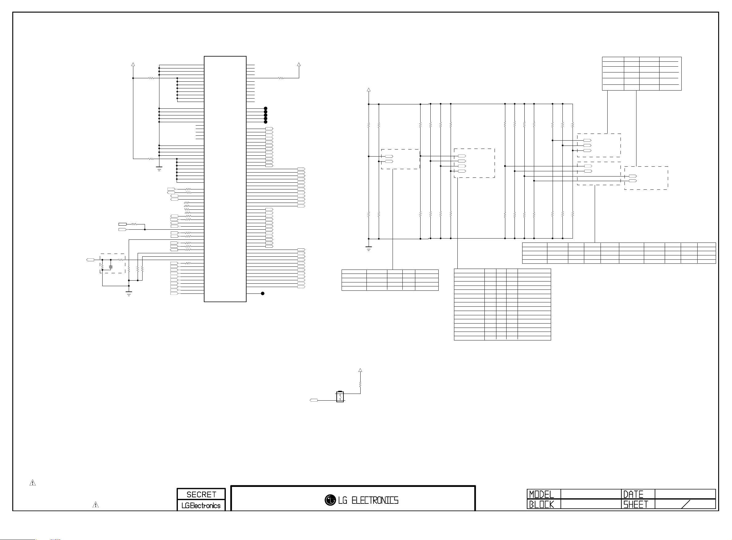
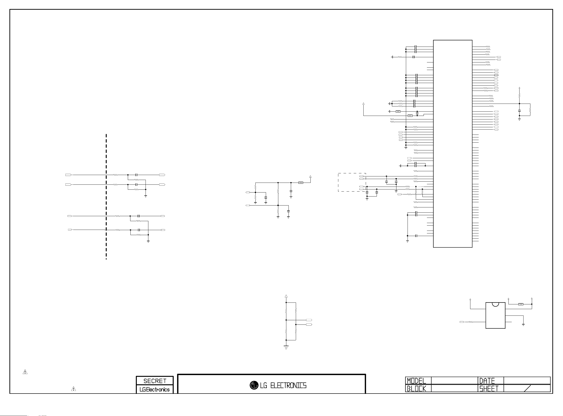
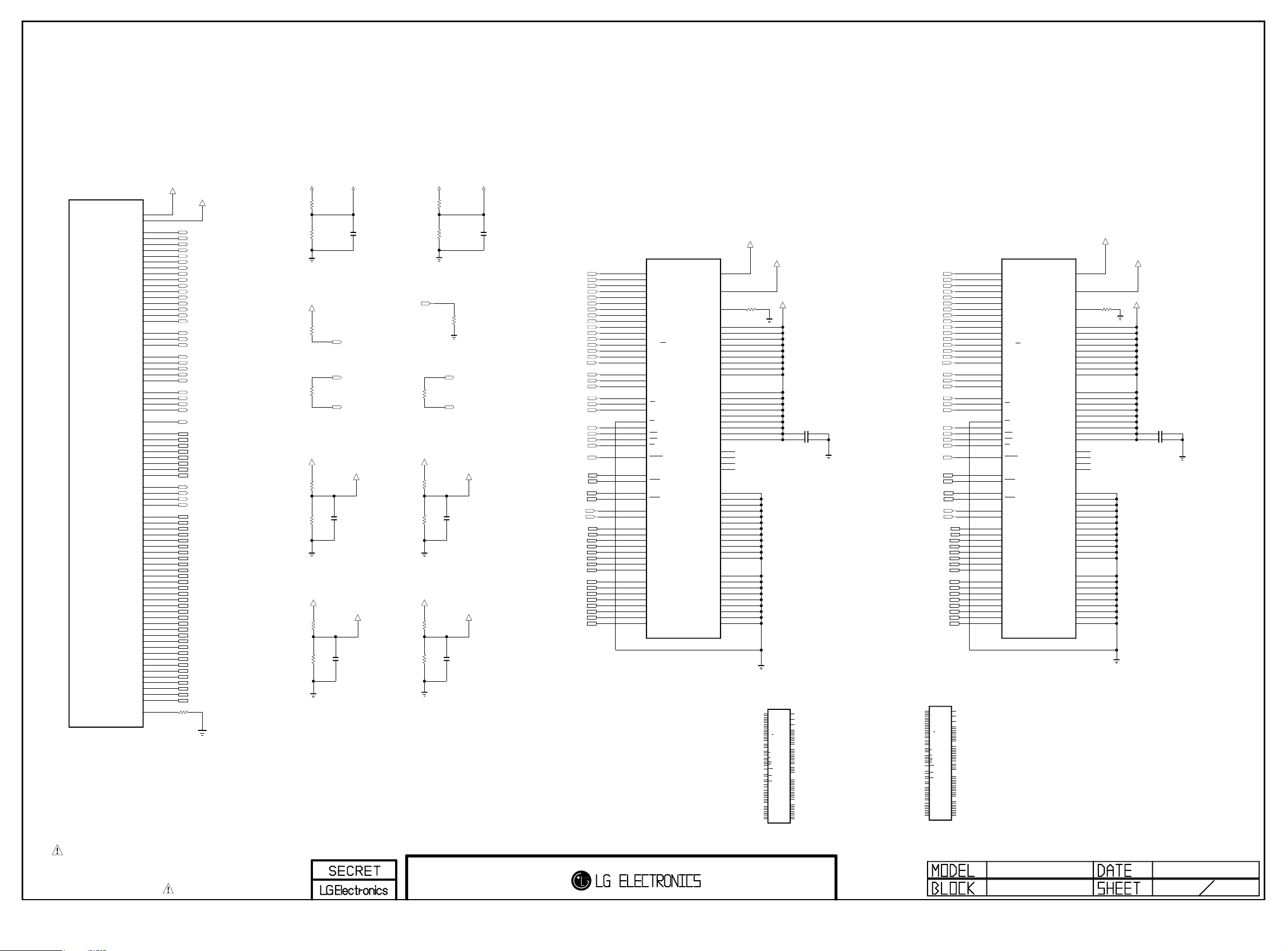
SCHEMATIC CIRCUIT DIAGRAM ..............................................................
Only for training and service purposes
- 2 -
LGE Internal Use OnlyCopyright © LG Electronics. Inc. All rights reserved.
Page 3
PRECAUTION
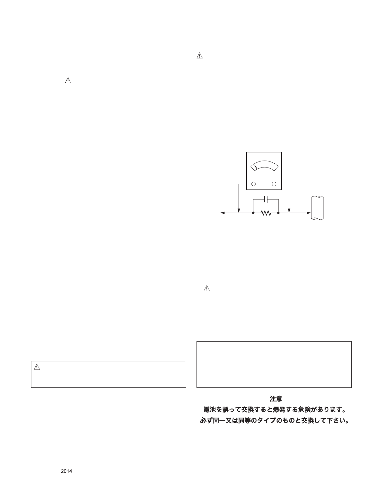
AC Volt-meter
WARNING FOR THE SAFETY-RELATED COMPONENT.
• There are some special components used in LCD
zmonitor that are important for safety. These parts are
marked on the schematic diagram and the
Exploded View. It is essential that these critical parts
should be replaced with the manufacturer' s specified
parts to prevent electric shock, fire or other hazard.
• Do not modify original design without obtaining written
permission from manufacturer or you will void the
original parts and labor guarantee.
TAKE CARE DURING HANDLING THE LCD MODULE
WITH BACKLIGHT UNIT.
• Must mount the module using mounting holes arranged
in four corners.
• Do not press on the panel, edge of the frame strongly or
electric shock as this will result in damage to the
screen.
• Do not scratch or press on the panel with any sharp
objects, such as pencil or pen as this may result in
damage to the panel.
• Protect the module from the ESD as it may damage the
electronic circuit (C-MOS).
• Make certain that treatment person' s body are grounded
through wrist band.
WARNING
BE CAREFUL ELECTRIC SHOCK !
• If you want to replace with the new backlight or inverter
circuit, must disconnect the AC adapter because high
voltage appears at inverter circuit about 650Vrms.
• Handle with care wires or connectors of the inverter
circuit. If the wires are pressed cause short and may
burn or take fire.
Leakage Current Hot Check Circuit
Good Earth Ground
such as WATER PIPE,
To Instrument's
exposed
METALLIC PARTS
When 25A is impressed between Earth and 2nd Ground
for 1 second, Resistance must be less than 0.1
*Base on Adjustment standard
0.15µF
1.5 Kohm/10W
CONDUIT etc.
• Do not leave the module in high temperature and in
areas of high humidity for a long time.
• The module not be exposed to the direct sunlight.
• Avoid contact with water as it may a short circuit within
the module.
• If the surface of panel become dirty, please wipe it off
with a softmaterial. (Cleaning with a dirty or rough cloth
may damage the panel.)
CAUTION
Please use only a plastic screwdriver to protect yourself
from shock hazard during service operation.
• Replaceable batteries
CAUTION
RISK OF EXPLOSION IF BATTERY IS REPLACED BY
AN INCORRECT TYPE.
DISPOSE OF USED BATTERIES ACCORDING TO
THE INSTRUCTIONS.
REPLACE ONLY WITH THE SAME OR EQUIVALENT
TYPE.
ADVARSEL
Lithiumbatteri - Eksplosionsfare ved fejlagtig
håndtering.
Udskiftning må kun ske med batteri af samme
fabrikat og type.
Levér det brugte batteri tilbage til leverandøren.
Only for training and service purposes
- 3 -
LGE Internal Use OnlyCopyright © LG Electronics. Inc. All rights reserved.
Page 4

SERVICING PRECAUTIONS
CAUTION: Before servicing receivers covered by this service
manual and its supplements and addenda, read and follow the
SAFETY PRECAUTIONS on page 3 of this publication.
NOTE: If unforeseen circumstances create conflict between the
following servicing precautions and any of the safety precautions on
page 3 of this publication, always follow the safety precautions.
Remember: Safety First.
General Servicing Precautions
1. Always unplug the receiver AC power cord from the AC power
source before;
a. Removing or reinstalling any component, circuit board
module or any other receiver assembly.
b. Disconnecting or reconnecting any receiver electrical plug or
other electrical connection.
c. Connecting a test substitute in parallel with an electrolytic
capacitor in the receiver.
CAUTION: A wrong part substitution or incorrect polarity
installation of electrolytic capacitors may result in an
explosion hazard.
2. Test high voltage only by measuring it with an appropriate high
voltage meter or other voltage measuring device (DVM,
FETVOM, etc) equipped with a suitable high voltage probe.
Do not test high voltage by "drawing an arc".
3. Do not spray chemicals on or near this receiver or any of its
assemblies.
4. Unl ess specified othe rwise in this service manua l, clean
electrical contacts only by applying the following mixture to the
contacts with a pipe cleaner, cotton-tipped stick or comparable
non-abrasive applicator; 10% (by volume) Acetone and 90% (by
volume) isopropyl alcohol (90%-99% strength)
CAUTION: This is a flammable mixture.
Unless specified otherwise in this service manual, lubrication of
contacts in not required.
5. Do not defeat any plug/socket B+ voltage interlocks with which
receivers covered by this service manual might be equipped.
6. Do not apply AC power to this instrument and/or any of its
electrical assemblies unless all solid-state device heat sinks are
correctly installed.
7. Always connect the test receiver ground lead to the receiver
chassis ground before connecting the test receiver positive
lead.
Always remove the test receiver ground lead last.
8. Use with this receiver only the test fixtures specified in this
service manual.
CAUTION: Do not connect the test fixture ground strap to any
heat sink in this receiver.
Electrostatically Sensitive (ES) Devices
Some semiconductor (solid-state) devices can be damaged easily
by static electricity. Such components com monly are called
Electrostatically Sensitive (ES) Devices. Examples of typical ES
devices are integrated circuits and some field-effect transistors and
semiconductor "chip" compon ents. The following techniques
should be used to help reduce the incide nce of component
damage caused by static by static electricity.
1. Immediately before handling any semiconductor component or
semiconductor-equipped assembly, drain off any electrostatic
charge on your body by touching a known earth ground.
Alter natively, obtain and wear a comme rcially availab le
discharging wrist strap device, which should be removed to
prevent potential shock reasons prior to applying power to the
unit under test.
2. After removing an electrical assembly equipped with ES
devices, place the assembly on a conductive surface such as
aluminum foil, to prevent electrostatic charge buildup or
exposure of the assembly.
3. Use only a grounded-tip soldering iron to solder or unsolder ES
devices.
4. Use only an anti-static type solder removal device. Some solder
removal devices not classified as "anti-static" can generate
electrical charges sufficient to damage ES devices.
5. Do not use freon-propelled chemicals. These can generate
electrical charges sufficient to damage ES devices.
6. Do not remove a replacement ES device from its protective
package until immediately before you are ready to install it.
(Most re pla cem ent ES dev ice s are packaged with leads
electrically shorted together by conductive foam, aluminum foil
or comparable conductive material).
7. Immediately before removing the protective material from the
leads of a replacement ES device, touch the protective material
to the chassis or circuit assembly into which the device will be
installed.
CAUTION: Be sure no power is applied to the chassis or circuit,
and observe all other safety precautions.
8. Mi nimiz e bodil y motio ns wh en h andli ng u npack ag ed
replacement ES devices. (Otherwise harmless motion such as
the brushing together of your clothes fabric or the lifting of your
foot from a carp eted floor can ge ner ate st atic electricit y
sufficient to damage an ES device.)
General Soldering Guidelines
1. Use a grounded-tip, low-wattage soldering iron and appropriate
tip size and shape that will maintain tip temperature within the
range or 500 ˚F to 600 ˚F.
2. Use an appropriate gauge of RMA resin-core solder composed
of 60 parts tin/40 parts lead.
3. Keep the soldering iron tip clean and well tinned.
4. Thoroughly clean the surfaces to be soldered. Use a mall wirebristle (0.5 inch, or 1.25cm) brush with a metal handle.
Do not use freon-propelled spray-on cleaners.
5. Use the following unsoldering technique
a. Allow the soldering iron tip to reach normal temperature.
(500 ˚F to 600 ˚F)
b. Heat the component lead until the solder melts.
c. Quickly draw the melted solder with an anti-static, suction-
type solder removal device or with solder braid.
CAUTION: Work quickly to avoid overheating the circuit
board printed foil.
6. Use the following soldering technique.
a. Allow the soldering iron tip to reach a normal temperature
(500 ˚F to 600 ˚F)
b. First, hold the soldering iron tip and solder the strand against
the component lead until the solder melts.
c. Quickly move the soldering iron tip to the junction of the
component lead and the printed circuit foil, and hold it there
only un til the solder fl ows onto and around both the
component lead and the foil.
CAUTION: Work quickly to avoid overheating the circuit
board printed foil.
d. Closely inspect the solder area and remove any excess or
splashed solder with a small wire-bristle brush.
Only for training and service purposes
- 4 -
LGE Internal Use OnlyCopyright © LG Electronics. Inc. All rights reserved.
Page 5

IC Remove/Replacement
Some chassis circuit boards have slotted holes (oblong) through
which the IC leads are inserted and then bent flat against the
circuit foil. When holes are the slotted type, the following technique
should be used to remove and replace the IC. When working with
boards using the familiar round hole, use the standard technique
as outlined in paragraphs 5 and 6 above.
Removal
1. Desolder and straighten each IC lead in one operation by gently
prying up on the lead with the soldering iron tip as the solder
melts.
2. Draw away the melted solder with an anti-static suction-type
solder removal device (or with solder braid) before removing the
IC.
Replacement
1. Carefully insert the replacement IC in the circuit board.
2. Carefully bend each IC lead against the circuit foil pad and
solder it.
3. Clean the soldered areas with a small wire-bristle brush.
(It is not necessary to reapply acrylic coating to the areas).
"Small-Signal" Discrete Transistor
Removal/Replacement
1. Remove the defective transistor by clipping its leads as close as
possible to the component body.
2. Bend into a "U" shape the end of each of three leads remaining
on the circuit board.
3. Bend into a "U" shape the replacement transistor leads.
4. Connect the replacement transistor leads to the corresponding
leads extending from the circuit board and crimp the "U" with
long nose pliers to insure metal to metal contact then solder
each connection.
CAUTION: Maintain original spacing between the replaced
component and adjacent components and the circuit board to
prevent excessive component temperatures.
Circuit Board Foil Repair
Excessive heat applied to the copper foil of any printed circuit
board will weaken the adhesive that bonds the foil to the circuit
board causing the foil to separate from or "lift-off" the board. The
following guidelines and procedures should be followed whenever
this condition is encountered.
At IC Connections
To repair a defective copper pattern at IC connections use the
following procedure to install a jumper wire on the copper pattern
si de of the circuit board. (Use this techniq ue onl y on IC
connections).
1. Carefully remove the damaged copper pattern with a sharp
knife. (Remove only as much copper as absolutely necessary).
2. carefully scratch away the solder resist and acrylic coating (if
used) from the end of the remaining copper pattern.
3. Bend a small "U" in one end of a small gauge jumper wire and
carefully crimp it around the IC pin. Solder the IC connection.
4. Route the jumper wire along the path of the out-away copper
pattern and let it overlap the previously scraped end of the good
copper pattern. Solder the overlapped area and clip off any
excess jumper wire.
At Other Connections
Use the following technique to repair the defective copper pattern
at connections other than IC Pins. This technique involves the
installation of a jumper wire on the component side of the circuit
board.
Power Output, Transistor Device
Removal/Replacement
1. Heat and remove all solder from around the transistor leads.
2. Remove the heat sink mounting screw (if so equipped).
3. Carefully remove the transistor from the heat sink of the circuit
board.
4. Insert new transistor in the circuit board.
5. Solder each transistor lead, and clip off excess lead.
6. Replace heat sink.
Diode Removal/Replacement
1. Remove defective diode by clipping its leads as close as
possible to diode body.
2. Bend the two remaining leads perpendicular y to the circuit
board.
3. Observing diode polarity, wrap each lead of the new diode
around the corresponding lead on the circuit board.
4. Securely crimp each connection and solder it.
5. Inspect (on the circuit board copper side) the solder joints of
the two "original" leads. If they are not shiny, reheat them and if
necessary, apply additional solder.
Fuse and Conventional Resistor
Removal/Replacement
1. Clip each fuse or resistor lead at top of the circuit board hollow
stake.
2. Securely crimp the leads of replacement component around
notch at stake top.
3. Solder the connections.
1. Remove the defective copper pattern with a sharp knife.
Remove at least 1/4 inch of copper, to ensure that a hazardous
condition will not exist if the jumper wire opens.
2. Trace along the copper pattern from both sides of the pattern
break an d loc ate the nearest component that is dir ect ly
connected to the affected copper pattern.
3. Connect insulated 20-gauge jumper wire from the lead of the
nearest component on one side of the pattern break to the lead
of the nearest component on the other side.
Carefully crimp and solder the connections.
CAUTION: Be sure the insulated jumper wire is dressed so the
it does not touch components or sharp edges.
Only for training and service purposes
- 5 -
LGE Internal Use OnlyCopyright © LG Electronics. Inc. All rights reserved.
Page 6
SPECIFICATION
1. Application range
This specication is applied to the LW43A chassis.
2. Requirement for Test
Each part is tested as below without special appointment.
1) Temperature: 25 °C ± 5 °C(77 °F ± 9 °F),
CST: 40 °C ± 5 °C
2) Relative Humidity: 65 % ± 10 %
3) Power Voltage
: Standard input voltage (AC 100-240 V~, 50/60 Hz)
* Standard Voltage of each products is marked by models.
4) Specication and performance of each parts are followed
each drawing and specication by part number in accord-
ance with BOM.
5) The receiver must be operated for about 5 minutes prior to
the adjustment.
3. Test method
1) Performance: LGE Monitor test method followed.
2) Demanded other specication
- Safety : CE, IEC specication
- EMC : CE, IEC
4. General Specication
4.1. General Specication
No. Item Content Remark
1 HDMI Input (2EA) HDMI Rear / support D-TV&PC
resolution
2 DVI Input (1EA) DVI
3 DP Input/Output(2EA) DP Rear / support D-TV&PC
resolution
4 Audio Input (1EA) DVI Audio L/R Input
5 Speaker Output (1EA) Compatible with common speaker 10W*2Ch Output
6 IR&Brightness Sensor Input
(1EA)
7 Pixel Sensor Input (1EA) Pixel Sensor Optional
8 External USB (1EA) Picture, Music, Movie, SVC Device : Memory Stick, Mouse,
9 RS-232C Input/Output
(1EA)
10 LAN(1EA) RJ45, 100BASE-T Network Connection for Super-
11 Local Key 8 keys
IR&Brightness Sensor
Keyboard
Display Control
Sign Elite
4.2. DVI-D, HDMI, Display Port (PC) Specication
No. Item Specication Remarks
1 Supported Sync. Type Digital
2 Operating Frequency Digital
3 Resolution Digital
Only for training and service purposes
Horizontal 30 ~ 83 kHz
Vertical 56 ~ 60 Hz
Max 1920×1080 @ 60Hz
Recommend 1920×1080 @ 60Hz
- 6 -
LGE Internal Use OnlyCopyright © LG Electronics. Inc. All rights reserved.
Page 7
5. Signal Timing (Supporting Resolution)
5.1. DVI, HDMI, Display Port (PC Mode )
No. Section Pol. Dot Clock
[MHz]
1 H(Pixels) - 25.175 31.469 800 640 16 96 48 640 x 480
V(Lines) - 59.94 525 480 10 2 33
2 H(Pixels) + 40.0 37.879 1056 800 40 128 88 800 x 600
V(Lines) + 60.317 628 600 1 4 23
3 H(Pixels) - 65.0 48.363 1344 1024 24 136 160 1024 x 768
V(Lines) - 60.0 806 768 3 6 29
4 H(Pixels) + 74.5 44.772 1664 1280 64 128 192 1280 x 720
V(Lines) + 59.855 748 720 3 5 20
5 H(Pixels) + 85.86 47.7 1800 1366 72 144 216 1366 x 768
V(Lines) + 60 795 768 1 3 23
6 H(Pixels) + 108.0 63.981 1688 1280 48 112 248 1280 x 1024
V(Lines) + 60.02 1066 1024 1 3 38
7 H(Pixels) - 146.25 65.290 2240 1680 104 176 280 1680 x 1050
V(Lines) + 59.954 1089 1050 3 6 30
8 H(Pixels) + 148.5 67.5 2200 1920 88 44 88 1920 x 1080
V(Lines) + 60 1125 1080 4 5 46
Frequency
[kHz]/[Hz]
Total
Cycle
(E)
Display
(A)
Front
Porch(B)
Sync.
(D)
Back
Porch(F)
Resolution
5.2. HDMI, DisplayPort (DTV Mode ) * DVI Input dont support DTV Mode
No.
Resolution H-freq(kHz) V-freq(Hz) Proposed
1 480/60P 31.5 60 EDTV 480p
2 576/50P 31.25 50 EDTV 576p
3 720/50P 37.5 50 HDTV 720p
4 720/60P 45 60 HDTV 720p
5 1080/50i 28.1 50 HDTV 1080i 50Hz For Australian
6 1080/60i 33.75 60 HDTV 1080i 60Hz
7 1080/50P 56.25 50 HDTV 1080P 50Hz
8 1080/60P 67.5 60 HDTV 1080P 60Hz
Specication Remark
Only for training and service purposes
- 7 -
LGE Internal Use OnlyCopyright © LG Electronics. Inc. All rights reserved.
Page 8
ADJUSTMENT INSTRUCTION
1. Application Range
This spec sheet is applied all of the Digital Signage Product
with LW43A chassis.
2. Specication
1) Because this is not a hot chassis, it is not necessary to
use an isolation transformer. However, the use of isolation
transformer will help protect test instrument.
2) Adjustment must be done in the correct order.
3) The adjustment must be performed in the circumstance of
25 °C ± 5 °C of temperature and 65 % ± 10 % of relative
humidity if there is no specic designation.
4) The input voltage of the receiver must keep AC 100-240
V~, 50/60 Hz.
5) At rst Worker must turn on the SET by using Power Only
key.
6) The receiver must be operated for about 5 minutes prior to
the adjustment when module is in the circumstance of over
15.
In case of keeping module is in the circumstance of 0 °C, it
should be placed in the circumstance of above 15 °C for 2
hours.
In case of keeping module is in the circumstance of below -20
°C, it should be placed in the circumstance of above 15 °C for
3 hours.
4. MAIN PCBA Adjustments
4.1. ADC Calibration [LS55A Model Digital
Only Model: does not apply]
- An ADC calibration is not necessary because MAIN
SoC (LGExxxx) is already calibrated from IC Maker
- If it needs to adjust manually, refer to appendix.
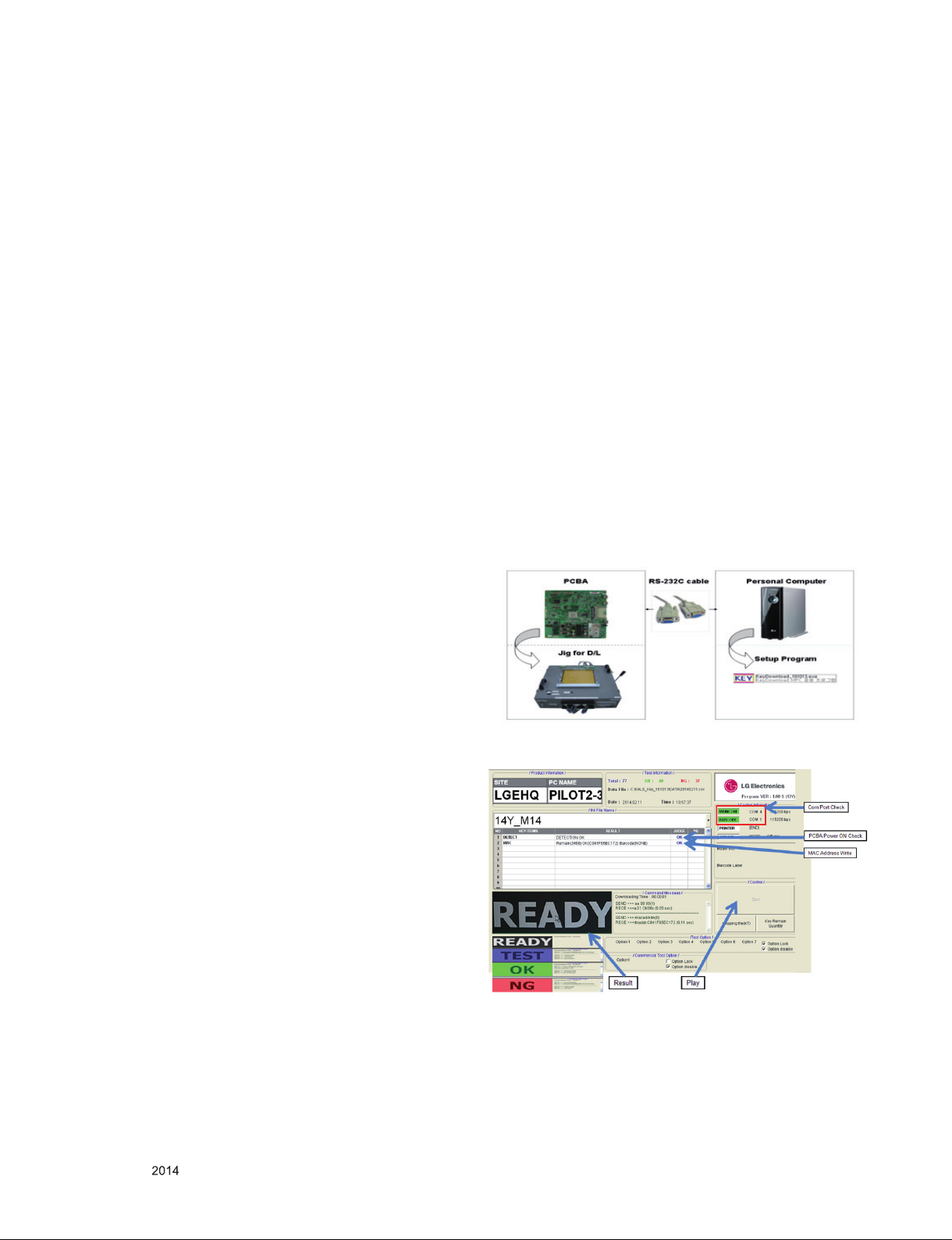
4.2. MAC Address
4.2.1. Equipment & Condition
1) Play le: keydownload.exe
4.2.2. Communication Port connection
1) Key Write: Com 1,2,3,4 and 115200 (Baudrate)
2) Barcode: Com 1,2,3,4 and 9600 (Baudrate)
4.2.3. Download process
1) Select the download items.
2) Mode check: Online Only
3) Check the test process : DETECT → MAC_WRITE
4) Play: START
5) Check of result: Ready, Test, OK or NG
4.2.4. Communication Port connection
1) Connect : PCBA Jig → RS-232C Port == PC → RS-232C
Port
Caution) When still image is displayed for a period of 20 minutes or longer (especially where W/B scale is strong. Digital
pattern 13ch and/or Cross hatch pattern 09ch), there can
some afterimage in the black level area
3. Adjustment items
3.1. Main PCBA Adjustments MAC Address
Download
1) ADC adjustment: Digital Only [does not apply]
2) EDID / DDC Download.
3) MAC Address Download
* Remark
- Above adjustment items can be also performed in
Final Assembly if needed. Adjustment items in both
PCBA and nal assembly stages can be checked by
using the INSTART Menu → ADJUST CHECK.
3.2. Final Assembly adjustment
1) White Balance adjustment
2) RS-232C functionality check
3) Factory Option setting per destination
4) Shipment mode setting (IN-STOP)
5) GND and HI-POT test
3.3. Appendix.
1) Ship-out mode
2) Service Option Default
3) Tool option menu, USB Download (S/W Update, Option,
service only)
4) ISP Download (Optional)
4.2.5. Download
Only for training and service purposes
- 8 -
LGE Internal Use OnlyCopyright © LG Electronics. Inc. All rights reserved.
Page 9
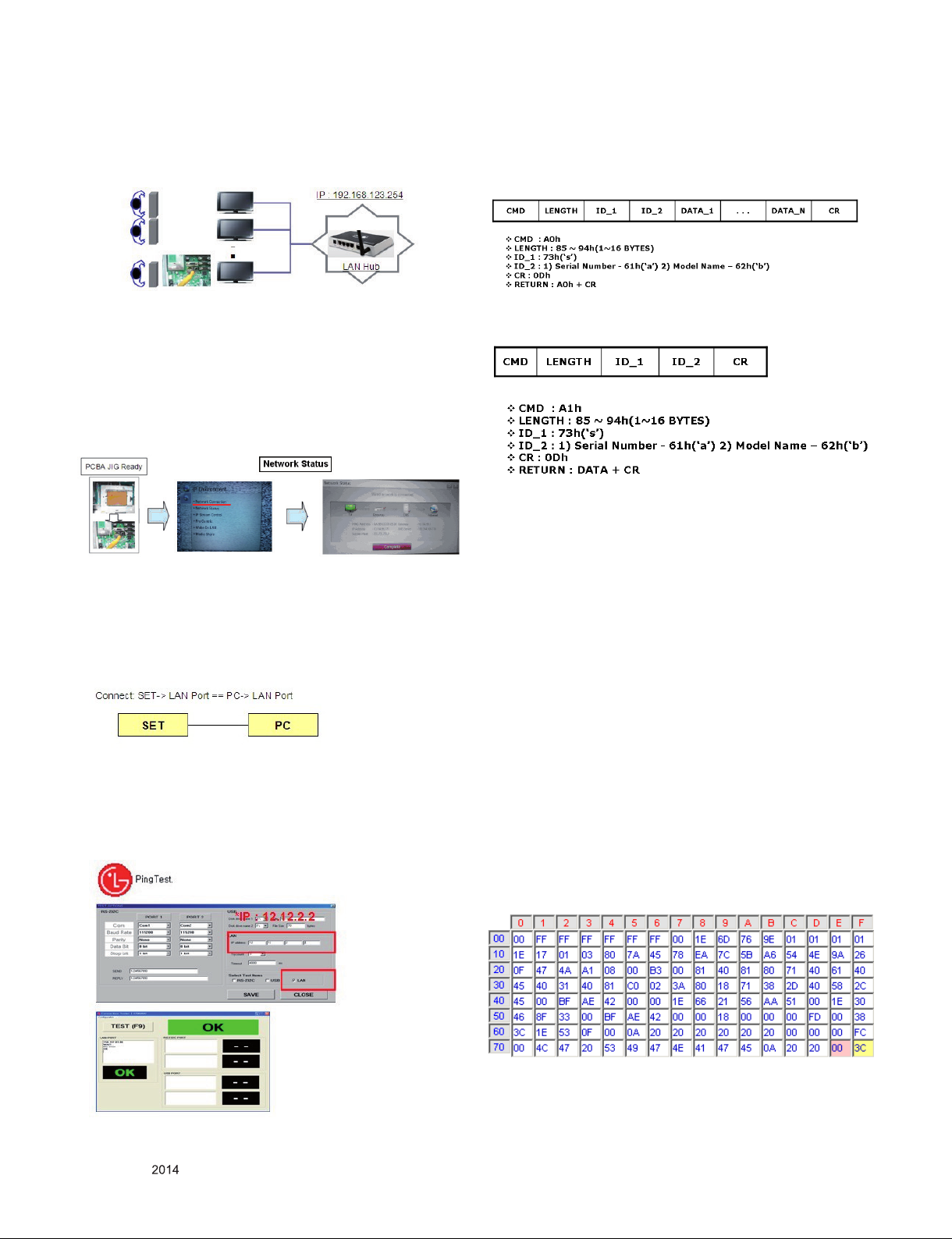
4.3. LAN Inspection
4.3.1. Equipment & Condition
▪ Each other connection to LAN Port of IP Hub and Jig
4.5 Serial number download
Connect Bar Code scan equipment and set by RS-232C
cable.
1) E2PROM Data Write
4.3.2. LAN inspection solution
1) LAN Port connection with PCB
2) Network setting at MENU Mode of SET (Installer Menu →
119 → 253 → Menu)
3) Setting automatic IP
4) Setting state conrmation
→ If automatic setting is nished, you conrm IP and MAC
Address.
4.4. LAN PORT INSPECTION(PING TEST)
4.4.1. Equipment setting
1) Play the LAN Port Test PROGRAM.
2) Input IP set up for an inspection to Test Program.
*IP Number : 12.12.2.2
4.4.2. LAN PORT inspection(PING TEST)
1) Play the LAN Port Test Program.
2) Connect each other LAN Port Jack.
3) Play Test (F9) button and conrm OK Message.
4) Remove LAN cable.
2) E2PROM Data Read
4.6 EDID/DDC Download (EDID PCM)
4.6.1 Overview
It is a VESA regulation. A PC or a MNT will display an optimal
resolution through information sharing without any necessity
of user input. It is a realization of “Plug and Play”.
4.6.2 Equipment
1) Since EDID data is embedded, EDID download JIG, HDMI
cable and D-sub are not need.
2) Adjust by using remote controller.
4.6.3 Download method
1) Press Adj. key on the Adj. R/C,
2) Select EDID D/L (PCM) menu.
3) By pressing Enter key, EDID download will begin
4) If Download is successful, OK is display, but If Download is
failure, NG is displayed.
5) If Download is failure, Re-try downloads.
→ Caution) When EDID Download, must remove HDMI / D-
sub Cable.
Only for training and service purposes
4.6.4. EDID DATA
1) DVI (Check Sum : 0x3C)
- 9 -
LGE Internal Use OnlyCopyright © LG Electronics. Inc. All rights reserved.
Page 10
2) HDMI 1 (Check Sum : 0x3E, 0xA2)
Color Analyzer
Computer
Pattern Generator
※
※If Signage internal pattern is us ed, not needed
Signal Source
Probe
RS-232C
RS-232C
RS-232C
3) HDMI 2 (Check Sum : 0x3E, 0x92)
5. Final Assembly Adjustment
5.1. White Balance Adjustment
5.1.1. Overview
5.1.1.1. W/B adj. Objective & How-it-works
1) Objective: To reduce each Panel's W/B deviation
2) How-it-works : When R/G/B gain in the OSD is at 192, it
means the panel is at its Full Dynamic Range. In order to
prevent saturation of Full Dynamic range and data, one of
R/G/B is xed at 192, and the other two is lowered to nd
the desired value.
3) Adjustment condition : normal temperature
- Surrounding Temperature : 25 °C ± 5 °C
- Warm-up time: About 5 Min
- Surrounding Humidity : 20 % ~ 80 %
- Before White balance adjustment, Keep power on
status, don’t power off
5.1.1.2. Adj. condition and cautionary items
1) Lighting condition in surrounding area surrounding lighting
should be lower 10 lux. Try to isolate adj. area into dark
surrounding.
2) Probe location: Color Analyzer (CA-210) probe should be
within 10cm and perpendicular of the module surface (80°~
100°)
3) Aging time
- After Aging Start, Keep the Power ON status during 5
Minutes.
- In case of LCD, Back-light on should be checked us-
ing no signal or Full-white pattern.
4) DP (Check Sum : 0x3C, 0xA2)
5.1.2. Equipment
1) Color Analyzer: CA-210 (NCG: CH 9 / WCG: CH12 / LED:
CH14)
2) Adj. Computer(During auto adj., RS-232C protocol is
needed)
3) Adjust Remocon
4) Video Signal Generator MSPG-925F 720p/204Gray(Model:217, Pattern:49)
* Only when internal pattern is not available
* Color Analyzer Matrix should be calibrated using CS-1000.
5.1.3. Equipment connection MAP
Only for training and service purposes
- 10 -
LGE Internal Use OnlyCopyright © LG Electronics. Inc. All rights reserved.
Page 11
5.1.4. Adj. Command (Protocol)
▪ RS-232C Command used during auto-adjustment.
RS-232C COMMAND
[CMD ID DATA]
wb 00 00 Begin White Balance adjustment
wb 00 ff
End White Balance adjustment
(internal pattern disappears )
Ex) wb 00 00 -> Begin white balance auto-adj.
wb 00 10 -> Gain adj.
ja 00 ff -> Adj. data
jb 00 c0
...
...
wb 00 1f → Gain adj. completed
*(wb 00 20(Start), wb 00 2f(end)) → Off-set adj.
wb 00 ff → End white balance auto-adj.
Explantion
4) Adjust Cool modes
- Fix the one of R/G/B gain to 192 (default data) and
decrease the others. ( If G gain is adjusted over 172
and R and B gain less than 192 , Adjust is O.K.)
- If G gain is less than 172, Increase G gain by up
to 172, and then increase R gain and G gain same
amount of increasing G gain.
- If R gain or B gain is over 255, Readjust G gain less
than 172, Conform to R gain is 255 or B gain is 255
5) Adj. is performed in COOL, MEDIUM, WARM 3 modes of
color temperature.
6) Adj. is completed, Exit adjust mode using “EXIT” key on
Remote controller.
▪ If internal pattern is not available, use RF input. In EZ Adj.
menu 6.White Balance, you can select one of 2 Test-pattern
: ON, OFF. Default is inner (ON). By selecting OFF, you can
adjust using RF signal in 206 Gray pattern.
▪ Adj. Map
Cool
Medium
Warm
Adj. item
R Gain j G 00 C0
G Gain j H 00 C0
B Gain j I 00 C0
R Cut
G Cut
B Cut
R Gain j A 00 C0
G Gain j B 00 C0
B Gain j C 00 C0
R Cut
G Cut
B Cut
R Gain j D 00 C0
G Gain j E 00 C0
B Gain j F 00 C0
R Cut
G Cut
B Cut
Command
(lower caseASCII)
CMD1 CMD2 MIN MAX
Data Range
(Hex.)
Default
(Decimal)
5.1.5. Adj. method
5.1.5.1. Auto adj. method
1) Set TV in adj. mode using POWER ON key.
2) Zero calibrate probe then place it on the center of the
Display.
3) Connect Cable.(RS-232C to USB)
4) Select mode in adj. Program and begin adj.
5) When adj. is complete (OK Sign), check adj. status pre
mode. (Warm, Medium, Cool)
6) Remove probe and RS-232C cable to complete adj.
▪ W/B Adj. must begin as start command “wb 00 00” , and n-
ish as end command “wb 00 ff”, and Adj. offset if need.
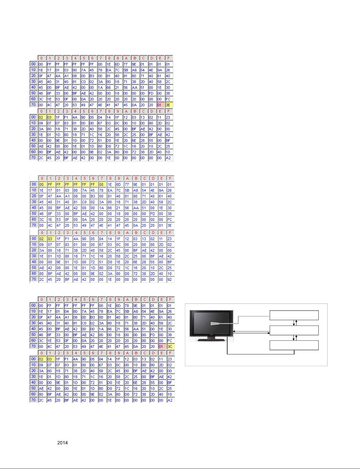
5.1.6. Reference (White balance Adj. coordinate and
color temperature)
▪ Luminance : 216 Gray
▪ Standard color coordinate and temperature using CA-210 (CH14)
: [applied only LGD Module]
Mode
Cool 0.271±0.002 0.270±0.002 13,000K -0.003
Medium 0.286±0.002 0.289±0.002 9,300K 0.0000
Warm 0.313±0.002 0.329±0.002 6,500K 0.0000
▪ Standard color coordinate and temperature using CA-210(CH 14)
– by aging time
1) ROW Direct LED models (applied only LGD Module) in LGEKR
(GUMI) And LGERS
Coordinate
x y
Temp ∆uv
5.1.5.2. Manual adjustment. method
1) Set TV in Adj. mode using POWER ON.
2) Zero Calibrate the probe of Color Analyzer, then place it on
the center of LCD module within 10 cm of the surface.
3) Press ADJ key → EZ adjust using adj. R/C → White-Balance then press the cursor to the right(key ►). When KEY
(►) is pressed 204 Gray (80IRE) internal patterns will be
displayed.
Only for training and service purposes
- 11 -
LGE Internal Use OnlyCopyright © LG Electronics. Inc. All rights reserved.
Page 12
2) ROW Direct LED models (applied only LGD Module) in LGEKR
(GUMI for Winter Season)
▪ Standard color coordinate and temperature using CA-
210(CH-14) – by aging time
5.3. Ship-out mode check (In-stop)
▪ After nal inspection, press In-Stop key of the Adj. R/C and
check that the unit goes to Stand-by mode
5) HI-POT test (Auto)
- If Test is failed, Buzzer operates.
- If Test is passed, GOOD Lamp on and move to next
process automatically.
7.3. Checkpoint
1) Test voltage
- GND: 1.5KV/min at 100mA
- SIGNAL: 3KV/min at 100mA
2) TEST time: 1 second
3) TEST POINT
- GND Test = POWER CORD GND and SIGNAL CABLE GND.
- Hi-pot Test = POWER CORD GND and LIVE & NEUTRAL.
4) LEAKAGE CURRENT: At 0.5mArms
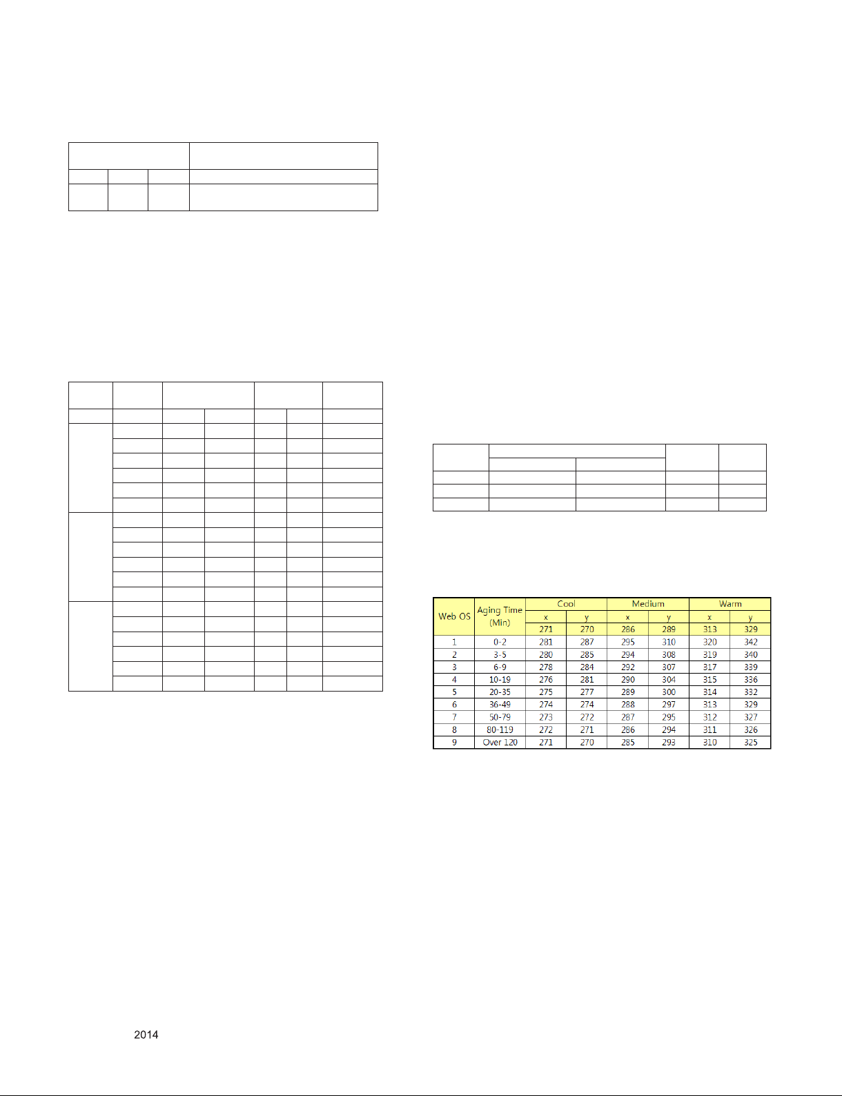
8. EYE Q Green Inspection
8.1 Method
[ Brightness + IR Sensor & Pixel Sensor ]
6. Audio
6.1. Audio input condition
1) Only DVI PC Input
6.2. Specication
No. Item Min Typ Max Unit Remark
Audio practical
max Output, L/R
1.
(Distortion=10%
max Output)
Speaker (8Ω
2.
Impedance)
9.0 10.0 12.0 W
8.5 8.9 9.8 Vrms
10.0 14.0 W
Measurement condition
EQ Off
AVL Off
Clear Voice Off
7. GND and HI-POT Test
7.1. GND & HI-POT auto-check preparation
1) Check the POWER CABLE and SIGNAL CABE insertion
condition
7.2. GND & HI-POT auto-check
1) Pallet moves in the station. (POWER CORD / AV CORD is
tightly inserted)
2) Connect the AV JACK Tester.
3) Controller (GWS103-4) on.
4) GND Test (Auto)
- If Test is failed, Buzzer operates.
- If Test is passed, execute next process (Hi-pot test).
Remove A/V CORD from A/V JACK BOX)
1) Connect the cable Assy on the set → 2) Turn on the Signage SET → 3) Press “EYE Button” on the adjustment of R/C
→ 4) Cover the “EYE Q sensor” on the front of Cable Assy
with your hands, hold it for 3 second
5) Check the sensor data on the screen, make certain that
data is below 20. If data isn’t below 20 in 3 seconds, EYE Q
sensor would be bad. You should change EYE Q sensor.
6) Uncover your hands from EYE Q sensor, hold it for 3 sec-
onds →
7) Check “Back Light(xxx)” on the screen, check data in-
crease, you should change EYE Q sensor
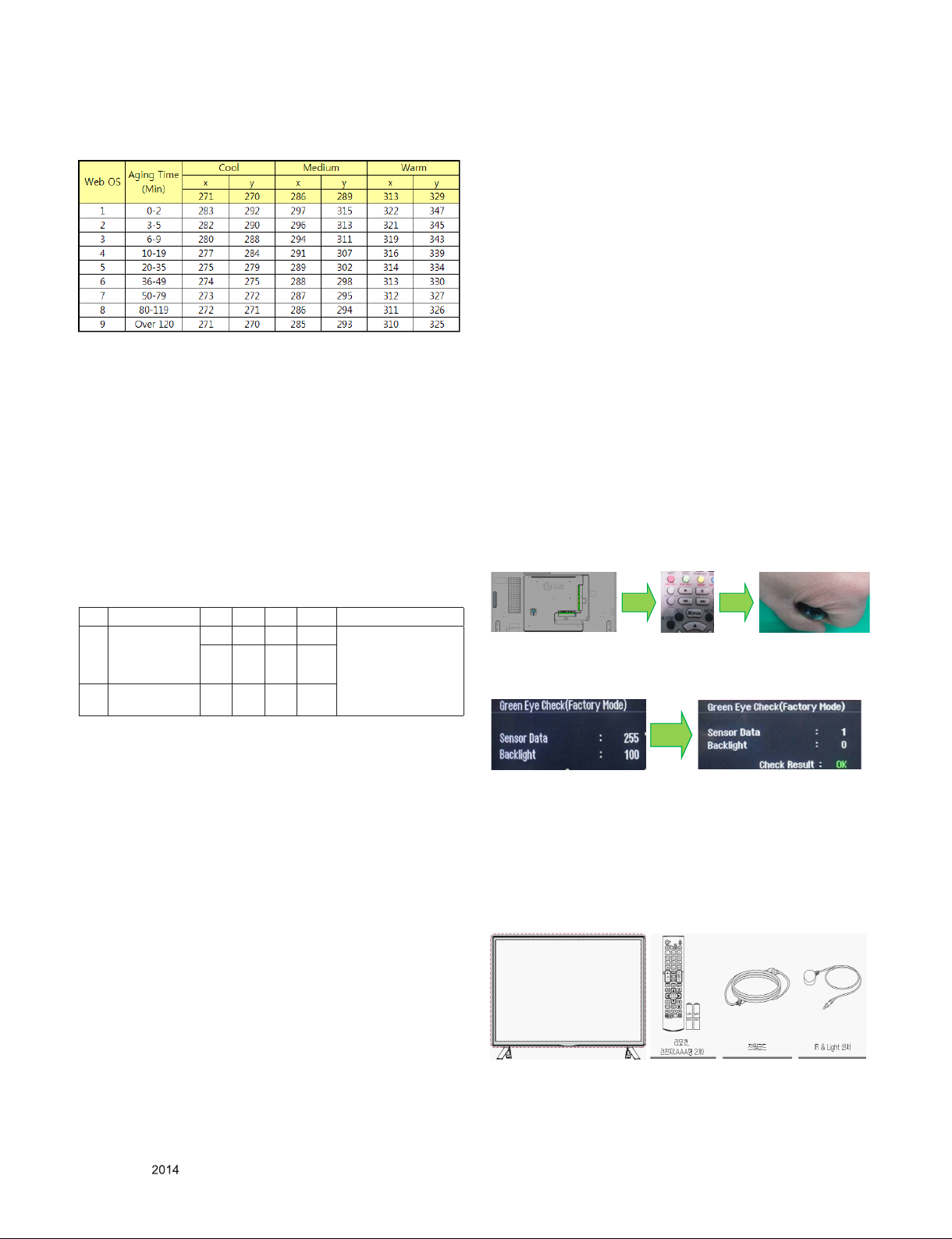
8.2 Pixel Sensor Inspection Manual
* Pixel Sensor Kit Parts
- 47LS55A SET / Power Cord / IR+Brightness Cable Assy /
Remote Control
Only for training and service purposes
- 12 -
LGE Internal Use OnlyCopyright © LG Electronics. Inc. All rights reserved.
Page 13
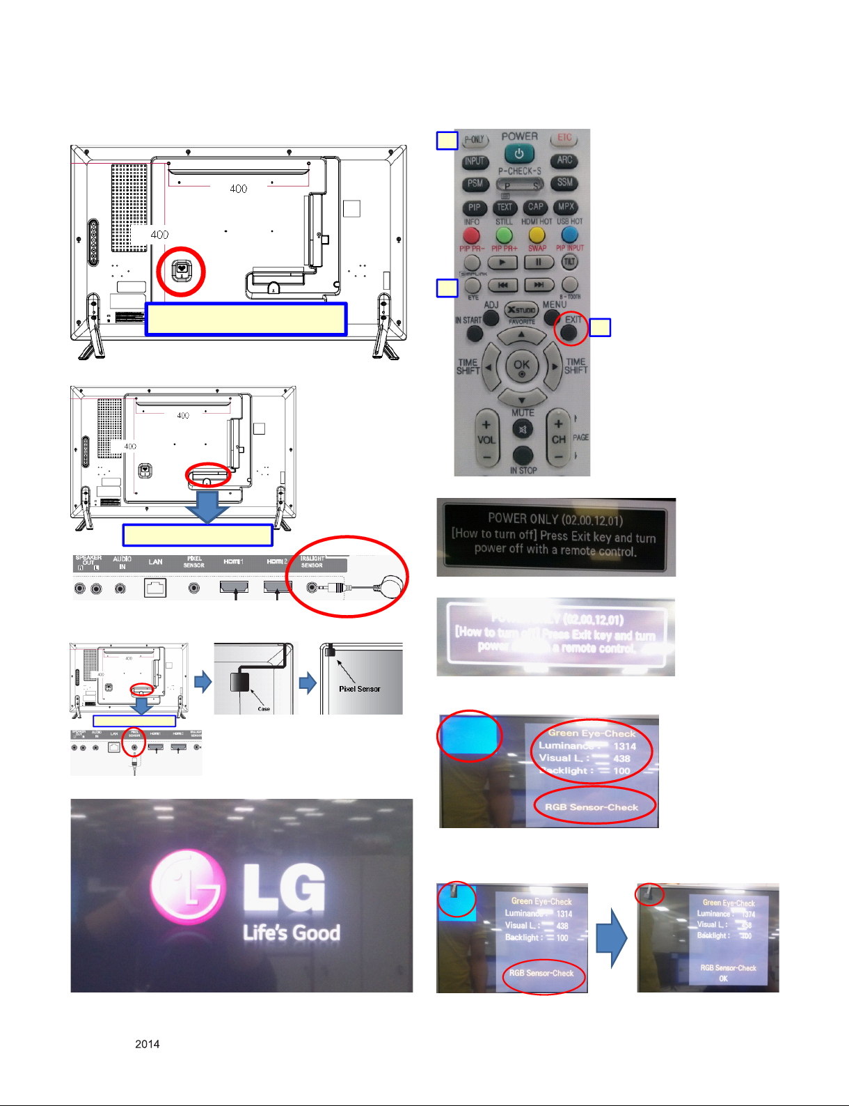
* Method
Power Cord Connection
IR+Brigntness Cable Connection
Pixel Sensor Cable
Connection
1
2
3
a
c
b
1) Connect the cable Assy[Power Cord] on the set.
2) Connect the cable Assy[IR+Brightness Cable] on the set.
5) As follows: the remote control operation.
a. Press " P-ONLY " on the adjustment of R/C.
3) Connect the cable Assy[Pixel Sensor Cable] on the set.
4) Turn on the Signage SET.
b. Press " EXIT " on the adjustment of R/C.
c. Press “EYE Button” on the adjustment of R/C
- Please Check the R,G,B pattern on the Screen.
- Check the sensor data on the screen
- Please check RGB Sensor-Check On the screen.
OK : Pass . NG : Fail [Re-Run]
Only for training and service purposes
- 13 -
LGE Internal Use OnlyCopyright © LG Electronics. Inc. All rights reserved.
Page 14
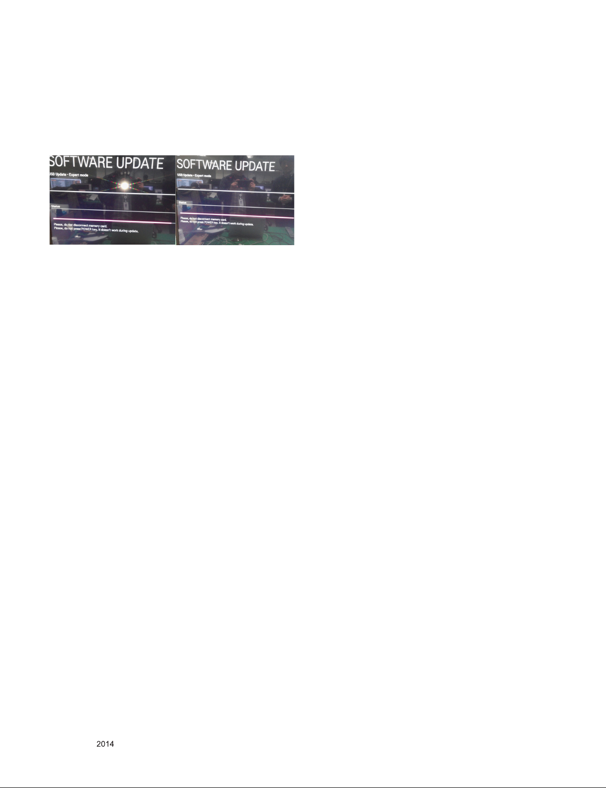
* USB S/W Download(Service only)
1) Put the USB Stick to the USB socket
2) Automatically detecting update le in USB Stick
- If your downloaded program version in USB Stick is
lower than that of Signage set, it didn’t work. Otherwise USB data is automatically detected.
3) Updating is staring.
4) Updating Completed, The Signage will restart automatically
5) If your Signage is turned on, check your updated version
and Tool option.(explain the Tool option, next stage)
* If downloading version is more high than your Signage
have, Signage can lost all channel data. In this case,
you have to channel recover. If all channel data is
cleared, you didn’t have a DTV/ATV test on production
line.
* After downloading, have to adjust Tool Option again.
1) Push "IN-START" key in service remote control.
2) Select "Tool Option 1" and push "OK" key.
3) Punch in the number. (Each model has their number)
Only for training and service purposes
- 14 -
LGE Internal Use OnlyCopyright © LG Electronics. Inc. All rights reserved.
Page 15
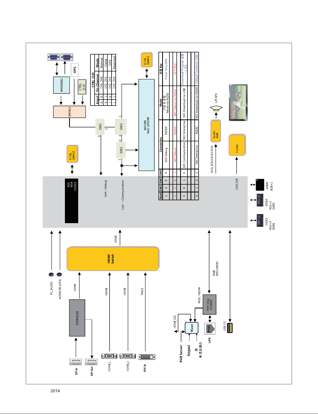
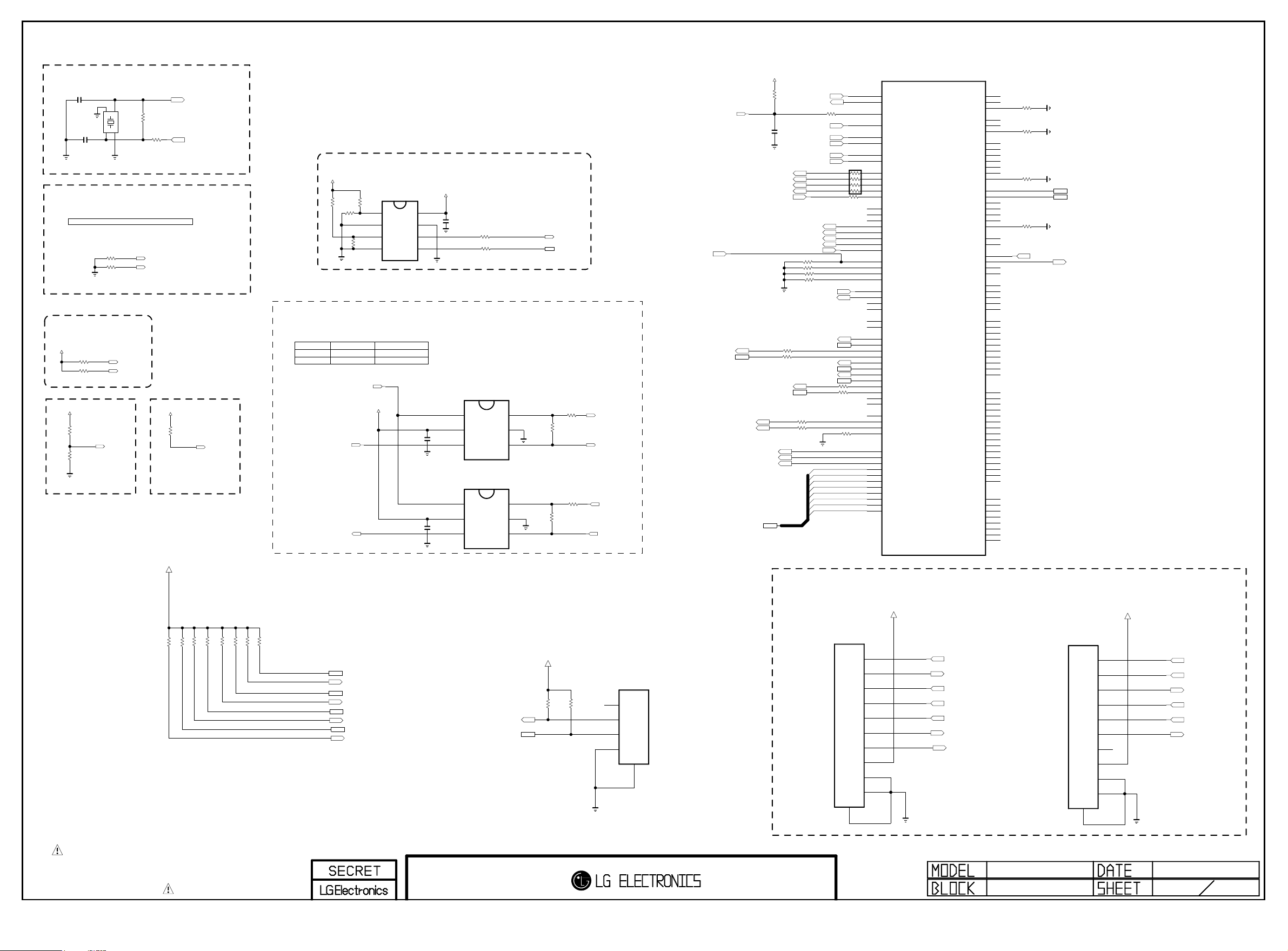
BLOCK DIAGRAM
Only for training and service purposes
- 15 -
LGE Internal Use OnlyCopyright © LG Electronics. Inc. All rights reserved.
Page 16
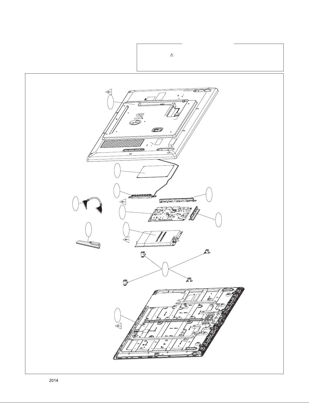
EXPLODED VIEW
Many electrical and mechanical parts in this chassis have special safety-related characteristics. These
parts are identified by in the Schematic Diagram and EXPLODED VIEW.
It is essenti al that these special safet y parts shoul d be replac ed with the same compo nents as
recommended in this manual to prevent X-RADIATION, Shock, Fire, or other Hazards.
Do not modify the original design without permission of manufacturer.
400
810
IMPORTANT SAFETY NOTICE
LV1
A2
510
200
541
540
542
530
201
Only for training and service purposes
- 16 -
LGE Internal Use OnlyCopyright © LG Electronics. Inc. All rights reserved.
Page 17
System Configuration
Copyright ⓒ 2014 LG Electronics. Inc. All right reserved.
Only for training and service purposes
LGE Internal Use Only
Clock for M14-A0
MAIN Clock(24Mhz)
50V
10pF
C101
50V
C102
System Clock for Analog block(24Mhz)
PLL SET[1:0] : internal pull up
"00" : CPU(1200Mhz),M0 / M1 DDR(792,792 Mhz)
"01" : CPU(1056Mhz),M0 / M1 DDR(672,672 Mhz)
"10" : CPU(1056Mhz),M0 / M1 DDR(792,792 Mhz)
"11" : CPU( 960Mhz),M0 / M1 DDR(792,792 Mhz)
OP MODE[1:0]
"00" : Normal Mode
"01/10/11" : Internal Test mode
+3.3V_NORMAL
OPT
R101 3.3K
R102 3.3K
OPT
Extenal test only
+3.3V_NORMAL
BOOT MODE
"0 : EMMC
"1 : TEST MODE
3.3K
R127
OPT
3.3K
R128
BOOT_MODE0
X-TAL_1
GND_1
1
2
24MHz
4
3
10pF
GND_2
X-TAL_2
Extenal test only
OPT
R103 3.3K
R104 3.3K
OPT
OPM1
OPM0
BOOT_MODE
X101
1M
R118
R8849
560
1%
PLLSET1
PLLSET0
INSTANT_MODE0
+3.3V_NORMAL
INSTANT boot MODE
3.3K
"1 : Instant boot
"0 : normal
(internal pull down)
R8843
XTAL_IN
XTAL_OUT
INSTANT_BOOT
NVRAM
+3.5V_ST
OPT
R110
4.7K
R111
OPT
0
AT24C1024BN-SH-T
R112
OPT
NC
1
A1
2
A2
3
GND
4
R8810
IC102
NVRAM I2C SWITCH
H
CONNECTION
B0 - AL
B1 - A
SCL_NVRAM
SDA_NVRAM
EEPROM_SW
NVRAM - NEC
NVRAM - M14
+3.5V_ST
EEPROM_SW
PAGE 1
+3.3V_NORMAL
R123
OPT
10K
XTAL_IN
XTAL_OUT
BOOT_MODE
PLLSET0
PLLSET1
OPM0
OPM1
TRST_N1
TMS1
TCK1
TDO1
TDI1
R182 10K
OPT
10K
R183
10K
R184
R185 10K
SOC_RX
SOC_TX
I2C_SCL1
I2C_SDA1
I2C_SCL2
I2C_SDA2
I2C_SCL4
I2C_SDA4
33
33
EMMC_DATA[7]
EMMC_DATA[6]
EMMC_DATA[5]
EMMC_DATA[4]
EMMC_DATA[3]
EMMC_DATA[2]
EMMC_DATA[1]
EMMC_DATA[0]
R109 33
AMP
R180 33
R181 33
R178 33
SOC_RESET
C108
0.1uF
16V
Write Protection
- Low : Normal Operation
+3.5V_ST
VCC
8
7
6
5
C105
WP
0.1uF
16V
SCL
SDA
- High : Write Protection
R113 33
R114 33
SCL_NVRAM
SDA_NVRAM
FORCED_JTAG_0
Sub Micom Ready
SUB1_SCL
SUB1_SDA
T-CON/L-DIMMING
L/DIM0_VS
L/DIM0_SCLK
TCK0
TDI0
L/DIM0_MOSI
READY
R117 22
R116 22
READY
Temp Sensor
I2C_SCL5
NVRAM
PWM_DIM2
PWM_DIM
EMMC_CLK
EMMC_CMD
EMMC_RST
EMMC_DATA[0-7]
I2C_SDA5
R107
R108
C103
0.1uF
16V
C104
0.1uF
16V
SELECT
VCC
SELECT
VCC
IC103
NLASB3157DFT2G
6
ON SEMICONDUCTOR
ANALOG SWITCH
5
A
4
EAN38256201
IC104
NLASB3157DFT2G
6
ON SEMICONDUCTOR
ANALOG SWITCH
5
A
4
EAN38256201
B1
1
GND
2
B0
3
B1
1
GND
2
B0
3
R121 0
OPT
R119 0
R122 0
OPT
R115 0
I2C_SCL5
NEC_EEPROM_SCL
I2C_SDA5
NEC_EEPROM_SDA
33
R179
10K
1/16W
5%
AR101
AG21
AJ18
AG30
AG28
AG29
AH29
AJ27
AH27
AG26
AH26
AJ12
AJ13
AH12
AG12
AH23
AG22
AH11
AG11
AG10
AH22
AJ22
AH10
AJ10
AG23
AH24
B23
A23
AB8
AC8
AD8
AE8
Y7
Y6
W7
W6
W5
AH7
AJ7
AG8
AH8
AH9
AG9
AJ9
AC6
AC7
AD7
AB7
G32
G33
G31
D31
F33
F32
E32
F31
D33
D32
E31
IC101
LG1311
XIN_MAIN
XO_MAIN
PORES_N
BOOT_MODE
PLLSET0
PLLSET1
OPM0
OPM1
L_VSOUT_LD/TRST0_N
DIM0_SCLK/TMS0
DIM1_SCLK/TCK0
DIM1_MOSI/TDI0
DIM0_MOSI/TDO0
SPI_CS0
SPI_SCLK0
SPI_DO0
SPI_DI0/TRST1_N
SPI_CS1/TMS1
SPI_SCLK1/TCK1
SPI_DO1/TDO1
SPI_DI1/TDI1
EXT_INTR0
EXT_INTR1
EXT_INTR2
EXT_INTR3
UART0_RXD
UART0_TXD
UART1_RXD
UART1_TXD
UART1_RTS_N
UART1_CTS_N
SCL0
SDA0
SCL1
SDA1
SCL2
SDA2
SCL3
SDA3
SCL4
SDA4
SCL5
SDA5
PWM0
PWM1
PWM2
PWM_IN
EMMC_CLK
EMMC_CMD
EMMC_RESETN
EMMC_DATA7
EMMC_DATA6
EMMC_DATA5
EMMC_DATA4
EMMC_DATA3
EMMC_DATA2
EMMC_DATA1
EMMC_DATA0
USB2_0_DP0
USB2_0_DM0
USB2_0_TXRTUNE
USB2_1_DP0
USB2_1_DM0
USB2_1_TXRTUNE
USB3_DP0
USB3_DM0
USB3_TXP0
USB3_TXM0
USB3_RXP0
USB3_RXM0
USB3_RESREF0
USB3_DP1
USB3_DM1
USB3_TXP1
USB3_TXM1
USB3_RXP1
USB3_RXM1
USB3_RESREF1
HUB_PORT_OVER0
HUB_VBUS_CTRL0
EB_CS3
EB_CS2
EB_CS1
EB_CS0
EB_WE_N
EB_OE_N
EB_WAIT
EB_BE_N1
EB_BE_N0
CAM_CD1_N
CAM_CD2_N
CAM_CE1_N
CAM_CE2_N
CAM_IREQ_N
CAM_RESET
CAM_INPACK_N
CAM_VCCEN_N
CAM_WAIT_N
CAM_REG_N
EB_ADDR0
EB_ADDR1
EB_ADDR2
EB_ADDR3
EB_ADDR4
EB_ADDR5
EB_ADDR6
EB_ADDR7
EB_ADDR8
EB_ADDR9
EB_ADDR10
EB_ADDR11
EB_ADDR12
EB_ADDR13
EB_ADDR14
EB_ADDR15
EB_DATA0
EB_DATA1
EB_DATA2
EB_DATA3
EB_DATA4
EB_DATA5
EB_DATA6
EB_DATA7
AN9
AM9
AN8
READY
H32
J31
H33
N31
N32
P33
P32
M32
M33
P31
K33
K32
L32
L31
K31
J32
M31
W28
W29
H28
J30
J28
J29
G30
F30
H29
G29
G28
P28
P27
U28
R29
V27
T28
T29
R28
U27
N29
K30
E30
M30
N28
M28
M29
L29
K29
K28
L28
D30
F29
C32
C33
C31
B33
B32
A32
B31
A31
A30
B30
C30
C29
R1712001%
READY
R1722001%
READY
R1732001%
R1742001%
/USB_OCD3
USB3_DP
USB3_DM
USB_CTL3
USB 2.0 : 1EA
+3.3V_NORMAL
I2C
I2C PULL UP
R161
3.3K
R162
3.3K
R158
3.3K
R157
3.3K
R125
3.3K
R120
3.3K
R124
3.3K
R126
3.3K
THE SYMBOL MARK OF THIS SCHEMETIC DIAGRAM INCORPORATES
SPECIAL FEATURES IMPORTANT FOR PROTECTION FROM X-RADIATION.
FIRE AND ELECTRICAL SHOCK HAZARDS, WHEN SERVICING IF IS
ESSENTIAL THAT ONLY MANUFACTURES SPECIFIED PARTS BE USED FOR
THE CRITICAL COMPONENTS IN THE SYMBOL MARK OF THE SCHEMETIC.
M14-Peripheral
I2C_1 : AMP
I2C_2 : T-CON,L/DIMING
I2C_3 : Temp Sensor
I2C_4 : NVRAM
I2C_SDA1
I2C_SCL1
I2C_SDA2
I2C_SCL2
I2C_SDA4
I2C_SCL4
I2C_SDA5
I2C_SCL5
LOCAL DIMMING I2C CONTROL
+3.3V_NORMAL
R105
R106
3.3K
3.3K
DEBUG
DEBUG
LED_SCL
LED_SDA
P102
12507WS-04L
DEBUG
1
2
3
4
5
Jtag-0 I/F
P103
12505WS-10A00
JTAG_CPU
1
2
3
4
5
6
7
8
9
10
11
+3.3V_NORMAL
L/DIM0_VS
(TRST0_N)
TDI0
L/DIM0_MOSI
L/DIM0_SCLK
TCK0
SOC_RESET
FORCED_JTAG_0
(TDO0)
(TMS0)
LS55A
M14 Symbol A
P104
12505WS-10A00
OPT
10
11
Jtag-1 I/F
+3.3V_NORMAL
1
2
3
4
5
6
7
8
9
TRST_N1
TDI1
TDO1
TMS1
TCK1
SOC_RESET
2013.10.21
1
36
Page 18
AMP_RESET_N
Copyright ⓒ 2014 LG Electronics. Inc. All right reserved.
Only for training and service purposes
LGE Internal Use Only
LED_SDA
INSTANT_BOOT
Near AMP 14.02.12
R233
4.7K
R8840
0
C8740
1000pF
50V
14.02.10
DVDD33
14.02.11
OPT
R8837
22
14.02.11
14.02.10
14.02.10
10K
R236
14.02.11
R232
10K
R231
10K
MODEL_OPT_11
14.02.11
INV_CTL
/RST_PHY
2D/3D_CTL
SOC_NEC_TX
SOC_NEC_RX
OPC_EN
14.02.10
LED_SCL
WARM_MODE
MODEL_OPT_12
MODEL_OPT_0
PANEL_CTL
MODEL_OPT_1
10K
10K
MODEL_OPT_2
MODEL_OPT_3
MODEL_OPT_4
R230
R235
MODEL_OPT_5
MODEL_OPT_6
MODEL_OPT_7
MODEL_OPT_8
MODEL_OPT_9
MODEL_OPT_10
14.02.10
DEBUG
14.02.10
14.02.10
R237
R8842
R214
R215
R8839
R213
R229
R228
R225 22
R226
R234
R203
R202
R201
IC101
LG1311
AH30
TP_DVB_CLK
AH32
TP_DVB_SOP
AH31
TP_DVB_VAL
AH33
TP_DVB_ERR
AM33
TP_DVB_DATA7
AL32
TP_DVB_DATA6
AL33
TP_DVB_DATA5
AK32
TP_DVB_DATA4
AK33
TP_DVB_DATA3
AK31
TP_DVB_DATA2
AJ30
TP_DVB_DATA1
AJ31
TP_DVB_DATA0
AL31
STPI0_CLK
AN32
STPI0_SOP
AM32
STPI0_VAL
AN31
STPI0_ERR
AM31
STPI0_DATA
AH28
STPI1_CLK
AJ28
STPI1_SOP
AK30
STPI1_VAL
AJ29
STPI1_ERR
AG27
STPI1_DATA
A28
TPI_CLK
B28
TPI_SOP
B29
TPI_VAL
C28
TPI_ERR
A27
TPI_DATA0
B27
TPI_DATA1
C27
TPI_DATA2
B26
TPI_DATA3
C26
TPI_DATA4
B25
TPI_DATA5
A25
TPI_DATA6
C25
TPI_DATA7
AG13
22
GPIO31
22
AJ19
GPIO30
AG14
GPIO29
AG15
GPIO28
AJ15
22
GPIO27
AH19
22
GPIO26
AH18
22
GPIO25
AG19
22
GPIO24
AH5
22
GPIO23
AJ5
22
GPIO22
AJ6
GPIO21
AH6
GPIO20
AG6
OPT
GPIO19
AG5
GPIO18
22
AF7
GPIO17
AG7
GPIO16
AG24
22
GPIO15
AH16
22
GPIO14
V29
22
GPIO13
AJ21
GPIO12
AH21
GPIO11
V28
GPIO10
AG16
22
GPIO9
AJ24
GPIO8
AH17
GPIO7
AG17
GPIO6
AH13
GPIO5
AH15
GPIO4
AG18
GPIO3
AH14
GPIO2
AJ16
GPIO1
AH20
GPIO0
TPIO_CLK
TPIO_SOP
TPIO_VAL
TPIO_ERR
TPIO_DATA0
TPIO_DATA1
TPIO_DATA2
TPIO_DATA3
TPIO_DATA4
TPIO_DATA5
TPIO_DATA6
TPIO_DATA7
EPI_SOE
EPI_MCLK
EPI_GCLK
EPI_EO
EPI_VST
TX_0N
TX_0P
TX_1N
TX_1P
TX_2N
TX_2P
TX_3N
TX_3P
TX_4N
TX_4P
TX_5N
TX_5P
TX_6N
TX_6P
TX_7N
TX_7P
TX_8N
TX_8P
TX_9N
TX_9P
TX_10N
TX_10P
TX_11N
TX_11P
TX_12N
TX_12P
TX_13N
TX_13P
TX_14N
TX_14P
TX_15N
TX_15P
TX_16N
TX_16P
TX_17N
TX_17P
TX_18N
TX_18P
TX_19N
TX_19P
TX_20N
TX_20P
TX_21N
TX_21P
TX_22N
TX_22P
TX_23N
TX_23P
TX_LOCKN
D28
E29
E28
F28
D27
E27
14.02.11
F27
E26
F26
E25
D25
F25
AA5
AB5
AA7
AA6
AB6
AK8
AL8
AK7
AL7
AM6
AN6
AK6
AL6
AK5
AL5
AN4
AN3
AM2
AM1
AM4
AM3
AL4
AL3
AK2
AK1
AK4
AK3
AJ4
AJ3
AH2
AH1
AH4
AH3
AG4
AG3
AF2
AF1
AF4
AF3
AE4
AE3
AD2
AD1
AD4
AD3
AC4
AC3
AB2
AB1
AB4
AB3
AA4
AA3
AM8
14.02.11
14.02.11
DVDD33
OPT
R8841
10K
TXB4N/TX0N
TXB4P/TX0P
TXB3N/TX1N
TXB3P/TX1P
TXBCLKN/TX2N
TXBCLKP/TX2P
TXB2N/TX3N
TXB2P/TX3P
TXB1N/TX4N
TXB1P/TX4P
TXB0N/TX5N
TXB0P/TX5P
TXD4N/TX12N
TXD4P/TX12P
TXD3N/TX13N
TXD3P/TX13P
TXDCLKN/TX14N
TXDCLKP/TX14P
TXD2N/TX15N
TXD2P/TX15P
TXD1N/TX16N
TXD1P/TX16P
TXD0N/TX17N
TXD0P/TX17P
TXA4N/TX6N
TXA4P/TX6P
TXA3N/TX7N
TXA3P/TX7P
TXACLKN/TX8N
TXACLKP/TX8P
TXA2N/TX9N
TXA2P/TX9P
TXA1N/TX10N
TXA1P/TX10P
TXA0N/TX11N
TXA0P/TX11P
TXC4N/TX18N
TXC4P/TX18P
TXC3N/TX19N
TXC3P/TX19P
TXCCLKN/TX20N
TXCCLKP/TX20P
TXC2N/TX21N
TXC2P/TX21P
TXC1N/TX22N
TXC1P/TX22P
TXC0N/TX23N
TXC0P/TX23P
+3.3V_NORMAL
BIT0_1
BIT0_0
MODEL_OPT_[0/1]
0 / 0
CHINA/HONGKONG
0 / 1
1 / 0
1 / 1
BIT1_1
R8823 10K
R8824 10K
10K
BIT1_0
R8825 10K
R8826
14.02.10
DVB
TAIWAN/COLOM
EU/CIS
ASIA/AFRICA
14.02.10
14.02.10
N/AMERICA
S/AMERCIA
MODEL_OPT_0
MODEL_OPT_1
AREA OPTION
ATSC
KOREA
JAPAN
MODEL_OPT_9
MODEL_OPT_10
MODEL_OPT_11
MODEL_OPT_12
Model Option
BIT2_1
R205 10K
BIT3_1
R207 10K
BIT4_1
R209 10K
BIT5_1
R211 10K
BIT6_1
R238 10K
BIT7_1
R240 10K
BIT11_1
R242 10K
BIT12_1
R244 10K
DDR3_DDP
MODEL_OPT_2
MODEL_OPT_3
MODEL_OPT_4
MODEL_OPT_5
14.02.10
BIT3_0
BIT2_0
14.02.12
JP
BIT4_0
BIT5_0
R206 10K
R210 10K
R208 10K
R212 10K
BACK-END OPTION
MODEL_OPT_[2/3/4/5]
0 / 0 / 0 / 0
0 / 0 / 0 / 1
0 / 0 / 1 / 0
0 / 0 / 1 / 1
0 / 1 / 0 / 0
0 / 1 / 0 / 1
0 / 1 / 1 / 0
0 / 1 / 1 / 1
1 / 0 / 0 / 0
1 / 0 / 0 / 1
1 / 0 / 1 / 0
1 / 0 / 1 / 1
1 / 1 / 0 / 0
1 / 1 / 0 / 1
1 / 1 / 1 / 0
1 / 1 / 1 / 1
TYPE
EPI FHD, 120Hz, V14 (8 lane)
EPI FHD, 120Hz, v14_32inch (6 lane)
EPI FHD, 120Hz, V13 (6 lane)
EPI FHD, 120Hz, V12 (6 lane)
EPI FHD, 60Hz, V14_32 inch (6lane)
LVDS FHD, 120Hz
LVDS FHD, 60Hz
LVDS HD, 60Hz
LVDS FHD, 60Hz, CP BOX
LVDS HD, 60Hz SMALL SMART
Vby1 FHD, 120Hz
Reserve
Reserve
Reserve
Reserve
Reserve
FHD
BIT6_0
R239 10K
BIT7_0
R241 10K
FRC
BIT11_0
BIT12_0
R243 10K
MODEL_OPT_[6/7]
0 / 0
0 / 1
1 / 0
1 / 1
PANEL TYPE
OLED,UD
R245 10K
DDR3_NON_DDP
T2/C/S2/ATV_EXT
T/C/S2/ATV_SOC
OPT
R217 10K
R221 10K
R219 10K
MODEL_OPT_8
MODEL_OPT_9
MODEL_OPT_10
MODEL_OPT_6
MODEL_OPT_7
OPT
R220 10K
R218 10K
EU/CIS KOREA
R222 10K
AJJA JAPAN
TAIWAN/COL
T/C
T2/C PIP
T2/C T2/C
T2/C/S2
T/C
T/C
T2/C PIP
T2/C
CHINA/HONG
Default
14.02.12
ATSC PIP
ATV_SOC
ATV_EXT
PAGE 2
HIGH
DDR3MODEL_OPT_8
MODEL_OPT_11
MODEL_OPT_12
14.02.12
DDP
14.02.12
NORTH AMERICA
ATSC PIP
ATV_SOC
ATV_EXT
LOW
NON_DDP
BRAZIL
ISDB PIP
ISDB
Default
THE SYMBOL MARK OF THIS SCHEMETIC DIAGRAM INCORPORATES
SPECIAL FEATURES IMPORTANT FOR PROTECTION FROM X-RADIATION.
FIRE AND ELECTRICAL SHOCK HAZARDS, WHEN SERVICING IF IS
ESSENTIAL THAT ONLY MANUFACTURES SPECIFIED PARTS BE USED FOR
M14-Display In/Out
THE CRITICAL COMPONENTS IN THE SYMBOL MARK OF THE SCHEMETIC.
DEBUG
+3.3V_NORMAL
SW201
JTP-1127WEM
12
3
4
For ISP
R223
3.3K
LS55A
M14 Symbol C
2013.10.21
2
36
Page 19
PLACE AT JACK SIDE
Copyright ⓒ 2014 LG Electronics. Inc. All right reserved.
Only for training and service purposes
LGE Internal Use Only
IC101
LG1311
PAGE 3
Place JACK Side
OPS_L_IN
OPS_R_IN
PC_L_IN
PC_R_IN
Place SOC Side
OPS AUDIO IN
R309 27K
R310 27K
C316 4.7uF
1%
1%
R322 10K
C317 4.7uF
R323 10K
AUDIO IN
R8816
27K
1%
R8817
27K
1%
10V
1%
10V
1%
C8721 4.7uF10V
10K1%
R8818
C8722 4.7uF10V
10K
1%
R8819
14.02.07
AUAD_L_CH3_IN
AUAD_R_CH3_IN
AUAD_L_CH2_IN
AUAD_R_CH2_IN
Placed as close as possible to IC101
R37 4
51K
AUAD_L_REF
1%
R37 8
47K
1%
C313
4.7uF
10V
R38 0
51K
1%
AUAD_R_REF
R38 1
47K
1%
C353
4.7uF
10V
C354
10uF
10V
L307
120-ohm
AVDD25
AUD_MASTER_CLK
AUD_LRCH
AUD_SCK
AUD_LRCK
MAIN I2S_I/F
AVDD25
AUDIO IN
OPS AUDIO IN
50V
C335
22pF
OPT
14.02.11
14.02.11
AUAD_L_CH2_IN
AUAD_R_CH2_IN
50V
C337
33pF
OPT
R8828
R8829 68
R8830 68
14.02.11
BLM15BD121SN1
R354 0
R355 0
AUAD_L_CH3_IN
AUAD_R_CH3_IN
50V
C340
22pF
OPT
I2S_AMP
14.02.11
R8827
68
14.02.11
14.02.11
L306
READY
READY
14.02.11
14.02.11
AUAD_R_REF
AUAD_L_REF
50V
C342
22pF
OPT
R368 100
R369
14.02.11
C8724
C8725 0.1uF 16V
C8726 0.1uF 16V
C8727 0.047uF25V
C8728
C8729
C8730
C8731
C8732
C8733
C8734
C8735 0.1uF16V
C8736
68
C8737 0.047uF25V
C8738 0.047uF25V
14.02.11
L305
BLM15BD121SN1
R361 0
R362 0
R363 0
R364 0
R372 0
R376 0
C348 2.2uF
R360 33
R365 100
R366 100
R367 0
100
R386
OPT
R370
R371
C8739
C351
C352 0.1uF
0.1uF 16V
0.1uF
0.1uF16V
0.1uF16V
0.1uF16V
0.1uF16V
0.1uF16V
0.1uF16V
0.047uF25V
C301
0.1uF
16V
OPT
OPT
OPT
OPT
READY
READY
10uF 10VC347
10V
OPT
R387
OPT
OPT
0
OPT
0
0.1uF16V
0.1uF
16V
16V
16V
R388
OPT
AL27
AK26
AM27
AL26
AN27
AL25
AM25
AN23
AL22
AK21
AK22
AL24
AK23
AL23
AK24
AL21
AM23
AN25
AM21
AN21
AK16
AL16
AL19
AK19
AN19
AM19
AN17
AM17
AL17
AK17
AK20
AL20
AK18
AL18
AN15
AM15
AN11
AK11
AK10
AL10
AL11
AM11
AK29
AL29
AM29
AK27
AL30
AK28
AL28
AN29
AD5
AE5
AE7
AE6
AD6
CVBS_IN1
CVBS_IN2
CVBS_IN3
CVBS_VCM
BUF_OUT1
SC1_SID
SC1_FB
SOY1_IN
Y1_IN
PB1_IN
PR1_IN
SOY2_IN
Y2_IN
PB2_IN
PR2_IN
ADC1_COM
ADC2_COM
ADC3_COM
AVSS25_COMP_REF
AVDD25_COMP_REF
AUDA_SCART_OUTL
AUDA_SCART_OUTR
AUAD_L_CH1_IN
AUAD_R_CH1_IN
AUAD_L_CH2_IN
AUAD_R_CH2_IN
AUAD_L_CH3_IN
AUAD_R_CH3_IN
AUAD_L_CH4_IN
AUAD_R_CH4_IN
AUDA_OUTL
AUDA_OUTR
AUAD_L_REF
AUAD_R_REF
AUD_VBG_EXT
IEC958OUT
AUDCLK_OUT
DAC_LRCH
DAC_SLRCH
DAC_CLFCH
DAC_SCK
DAC_LRCK
PCMI3LRCH
PCMI3LRCK
PCMI3SCK
AUDCLK_IN
FRC_LRSYNC
AAD_ADC_SIF
AAD_ADC_SIFM
IFAGC
DMD_DAC_OUT
DMD_SIF_OUT
DMD_ADC_INP
DMD_ADC_INN
DMD_ADC_INCOM
SD_CLK
SD_CMD
SD_CD_N
SD_WP_N
SD_DATA3
SD_DATA2
SD_DATA1
SD_DATA0
RMII_REF_CLK
RMII_CRS_DV
RMII_MDIO
RMII_MDC
RMII_TXEN
RMII_TXD1
RMII_TXD0
RMII_RXD1
RMII_RXD0
HDMI_1_SCL
HDMI_1_SDA
HDMI_1_HPD
HDMI_1_5V_DET
HDMI_1_ARC
HDMI_1_RX_0
HDMI_1_RX_0B
HDMI_1_RX_1
HDMI_1_RX_1B
HDMI_1_RX_2
HDMI_1_RX_2B
HDMI_1_RX_C
HDMI_1_RX_CB
HDMI_2_SCL
HDMI_2_SDA
HDMI_2_HPD
HDMI_2_5V_DET
HDMI_2_RX_0
HDMI_2_RX_0B
HDMI_2_RX_1
HDMI_2_RX_1B
HDMI_2_RX_2
HDMI_2_RX_2B
HDMI_2_RX_C
HDMI_2_RX_CB
HDMI_3_SCL
HDMI_3_SDA
HDMI_3_HPD
HDMI_3_5V_DET
HDMI_3_RX_0
HDMI_3_RX_0B
HDMI_3_RX_1
HDMI_3_RX_1B
HDMI_3_RX_2
HDMI_3_RX_2B
HDMI_3_RX_C
HDMI_3_RX_CB
HDMI_4_SCL
HDMI_4_SDA
HDMI_4_CBUS_HPD
HDMI_4_CD_SENSE
HDMI_4_5V_DET
HDMI_4_RX_0
HDMI_4_RX_0B
HDMI_4_RX_1
HDMI_4_RX_1B
HDMI_4_RX_2
HDMI_4_RX_2B
HDMI_4_RX_C
HDMI_4_RX_CB
E22
D22
F22
F24
D24
E24
F23
E23
AK14
AK12
AL12
AK13
AL13
AM13
AN13
AL14
AK15
AE27
AF28
AE29
AF27
AE28
AF33
AF32
AE31
AE30
AD31
AD30
AF31
AF30
AD28
AD29
AC27
AD27
AC31
AC30
AB33
AB32
AA31
AA30
AD32
AD33
AB28
AB27
AB29
AC28
Y32
Y33
W31
W30
V33
V32
Y31
Y30
Y27
AA28
Y28
AA29
AA27
T31
T30
T32
T33
R31
R30
U31
U30
R327 0
R329 0
R328 0
R325 0
R324 0
R326 0
R315 33
R316 33
R375 33
R373 33
R300 33
R377 33
OPT
OPT
OPT
OPT
OPT
OPT
EPHY_REFCLK
EPHY_CRS_DV
EPHY_MDIO
EPHY_MDC
EPHY_EN
EPHY_TXD1
EPHY_TXD0
EPHY_RXD1
EPHY_RXD0
READY
READY
READY
READY
HDMI_RX0+
HDMI_RX0HDMI_RX1+
HDMI_RX1HDMI_RX2+
HDMI_RX2HDMI_CLK+
HDMI_CLK-
DDR3_OPT1
DDR3_OPT2
+5V_HDMI
R331
10
C302
1uF
10V
R33 0
5.1 K
THE SYMBOL MARK OF THIS SCHEMETIC DIAGRAM INCORPORATES
SPECIAL FEATURES IMPORTANT FOR PROTECTION FROM X-RADIATION.
FIRE AND ELECTRICAL SHOCK HAZARDS, WHEN SERVICING IF IS
ESSENTIAL THAT ONLY MANUFACTURES SPECIFIED PARTS BE USED FOR
THE CRITICAL COMPONENTS IN THE SYMBOL MARK OF THE SCHEMETIC.
M14-AV In/Out
DDR3 VENDOR OPTION
+3.3V_NORMAL
4.7K
4.7K
R384
R382
OPT
OPT
R385 4.7K
R383 4.7K
DDR3_OPT1
DDR3_OPT2
HDMI_EN
LS55A
M14 Symbol B
+5V_ST
OPT
R389
33
IN
EN
AP2151WG-7
5
4
IC381
+5V_NORMAL
OPT
PZ1608U121-2R0TF
OUT
1
GND
2
FLG
3
2013.10.21
14.02.07
L8702
3
+5V_HDMI
36
Page 20
PAGE 4
Copyright ⓒ 2014 LG Electronics. Inc. All right reserved.
Only for training and service purposes
LGE Internal Use Only
IC101
LG1311
M0_DDR_VREF1
M0_DDR_VREF2
M0_DDR_U_CLKP
M0_DDR_U_CLKN
M0_DDR_D_CLKP
M0_DDR_D_CLKN
M0_DDR_RESET_N
M0_DDR_DQS_P0
M0_DDR_DQS_N0
M0_DDR_DQS_P1
M0_DDR_DQS_N1
M0_DDR_DQS_P2
M0_DDR_DQS_N2
M0_DDR_DQS_P3
M0_DDR_DQS_N3
M0_DDR_ZQCAL
M0_DDR_A0
M0_DDR_A1
M0_DDR_A2
M0_DDR_A3
M0_DDR_A4
M0_DDR_A5
M0_DDR_A6
M0_DDR_A7
M0_DDR_A8
M0_DDR_A9
M0_DDR_A10
M0_DDR_A11
M0_DDR_A12
M0_DDR_A13
M0_DDR_A14
M0_DDR_A15
M0_DDR_BA0
M0_DDR_BA1
M0_DDR_BA2
M0_DDR_CKE
M0_DDR_ODT
M0_DDR_RASN
M0_DDR_CASN
M0_DDR_WEN
M0_DDR_DM0
M0_DDR_DM1
M0_DDR_DM2
M0_DDR_DM3
M0_DDR_DQ0
M0_DDR_DQ1
M0_DDR_DQ2
M0_DDR_DQ3
M0_DDR_DQ4
M0_DDR_DQ5
M0_DDR_DQ6
M0_DDR_DQ7
M0_DDR_DQ8
M0_DDR_DQ9
M0_DDR_DQ10
M0_DDR_DQ11
M0_DDR_DQ12
M0_DDR_DQ13
M0_DDR_DQ14
M0_DDR_DQ15
M0_DDR_DQ16
M0_DDR_DQ17
M0_DDR_DQ18
M0_DDR_DQ19
M0_DDR_DQ20
M0_DDR_DQ21
M0_DDR_DQ22
M0_DDR_DQ23
M0_DDR_DQ24
M0_DDR_DQ25
M0_DDR_DQ26
M0_DDR_DQ27
M0_DDR_DQ28
M0_DDR_DQ29
M0_DDR_DQ30
M0_DDR_DQ31
VREF_M0_0
A22
A3
E13
E11
E15
E17
D8
D16
D9
E16
E9
E14
D7
D10
D11
D14
E10
E12
D17
E8
D13
C8
B8
C17
B17
D12
E19
D19
D18
E18
D15
B18
C18
B16
A16
B9
C9
B7
A7
A15
A18
A6
A9
B20
B13
C21
C14
A21
A13
B21
C13
B14
B19
C15
C20
C16
A19
B15
C19
B11
C5
C12
B4
A12
A4
B12
C4
B5
B10
C6
C11
C7
A10
B6
C10
E7
VREF_M0_1
R401 240
M0_DDR_A0
M0_DDR_A1
M0_DDR_A2
M0_DDR_A3
M0_DDR_A4
M0_DDR_A5
M0_DDR_A6
M0_DDR_A7
M0_DDR_A8
M0_DDR_A9
M0_DDR_A10
M0_DDR_A11
M0_DDR_A12
M0_DDR_A13
M0_DDR_A14
M0_DDR_A15
M0_DDR_BA0
M0_DDR_BA1
M0_DDR_BA2
M0_U_CLK
M0_U_CLKN
M0_D_CLK
M0_D_CLKN
M0_DDR_CKE
M0_DDR_ODT
M0_DDR_RASN
M0_DDR_CASN
M0_DDR_WEN
M0_DDR_RESET_N
M0_DDR_DQS0
M0_DDR_DQS_N0
M0_DDR_DQS1
M0_DDR_DQS_N1
M0_DDR_DQS2
M0_DDR_DQS_N2
M0_DDR_DQS3
M0_DDR_DQS_N3
M0_DDR_DM0
M0_DDR_DM1
M0_DDR_DM2
M0_DDR_DM3
M0_DDR_DQ0
M0_DDR_DQ1
M0_DDR_DQ2
M0_DDR_DQ3
M0_DDR_DQ4
M0_DDR_DQ5
M0_DDR_DQ6
M0_DDR_DQ7
M0_DDR_DQ8
M0_DDR_DQ9
M0_DDR_DQ10
M0_DDR_DQ11
M0_DDR_DQ12
M0_DDR_DQ13
M0_DDR_DQ14
M0_DDR_DQ15
M0_DDR_DQ16
M0_DDR_DQ17
M0_DDR_DQ18
M0_DDR_DQ19
M0_DDR_DQ20
M0_DDR_DQ21
M0_DDR_DQ22
M0_DDR_DQ23
M0_DDR_DQ24
M0_DDR_DQ25
M0_DDR_DQ26
M0_DDR_DQ27
M0_DDR_DQ28
M0_DDR_DQ29
M0_DDR_DQ30
M0_DDR_DQ31
1%
+1.5V_DDR
+1.5V_DDR
OPT
+1.5V_DDR
+1.5V_DDR
R402
1K
1%
R403
1K
1%
R404
10K
R405
100
M0_DDR_VREFCA
R406
1K
1%
R407
1K
1%
M0_DDR_VREFDQ
R408
1K
1%
R409
1K
1%
VREF_M0_0
C401
0.1uF
16V
M0_DDR_RESET_N
M0_D_CLK
M0_D_CLKN
C402
0.1uF
16V
C403
0.1uF
16V
M0_DDR_CKE
+1.5V_DDR
R410
100
+1.5V_DDR
R411
1K
1%
R412
1K
1%
+1.5V_DDR
R413
1K
1%
R414
1K
1%
VREF_M0_1
R415
1K
1%
R416
1K
1%
R417
10K
M0_U_CLK
M0_U_CLKN
M0_1_DDR_VREFCA
C406
0.1uF
16V
M0_1_DDR_VREFDQ
C407
0.1uF
16V
C408
0.1uF
16V
M0_DDR_A0
M0_DDR_A1
M0_DDR_A2
M0_DDR_A3
M0_DDR_A4
M0_DDR_A5
M0_DDR_A6
M0_DDR_A7
M0_DDR_A8
M0_DDR_A9
M0_DDR_A10
M0_DDR_A11
M0_DDR_A12
M0_DDR_A13
M0_DDR_A14
M0_DDR_A15
M0_DDR_BA0
M0_DDR_BA1
M0_DDR_BA2
M0_D_CLK
M0_D_CLKN
M0_DDR_CKE
M0_DDR_ODT
M0_DDR_RASN
M0_DDR_CASN
M0_DDR_WEN
M0_DDR_RESET_N
M0_DDR_DQS0
M0_DDR_DQS_N0
M0_DDR_DQS1
M0_DDR_DQS_N1
M0_DDR_DM0
M0_DDR_DM1
M0_DDR_DQ0
M0_DDR_DQ1
M0_DDR_DQ2
M0_DDR_DQ3
M0_DDR_DQ4
M0_DDR_DQ5
M0_DDR_DQ6
M0_DDR_DQ7
M0_DDR_DQ8
M0_DDR_DQ9
M0_DDR_DQ10
M0_DDR_DQ11
M0_DDR_DQ12
M0_DDR_DQ13
M0_DDR_DQ14
M0_DDR_DQ15
IC401
H5TQ4G63AFR-PBC
DDR3
N3
P7
P3
N2
P8
P2
R8
R2
T8
R3
L7
R7
N7
T3
T7
M7
M2
N8
M3
J7
K7
K9
L2
K1
J3
K3
L3
T2
F3
G3
C7
B7
E7
D3
E3
F7
F2
F8
H3
H8
G2
H7
D7
C3
C8
C2
A7
A2
B8
A3
4Gbit
A0
(x16)
A1
DDR_512MB_HYNIX_1600_29n
A2
A3
A4
A5
A6
A7
A8
A9
A10/AP
A11
A12/BC
A13
A14
A15
BA0
BA1
BA2
CK
CK
CKE
CS
ODT
RAS
CAS
WE
RESET
DQSL
DQSL
DQSU
DQSU
DML
DMU
DQL0
DQL1
DQL2
DQL3
DQL4
DQL5
DQL6
DQL7
DQU0
DQU1
DQU2
DQU3
DQU4
DQU5
DQU6
DQU7
VREFCA
VREFDQ
VDD_1
VDD_2
VDD_3
VDD_4
VDD_5
VDD_6
VDD_7
VDD_8
VDD_9
VDDQ_1
VDDQ_2
VDDQ_3
VDDQ_4
VDDQ_5
VDDQ_6
VDDQ_7
VDDQ_8
VDDQ_9
NC_1
NC_2
NC_3
NC_4
VSS_1
VSS_2
VSS_3
VSS_4
VSS_5
VSS_6
VSS_7
VSS_8
VSS_9
VSS_10
VSS_11
VSS_12
VSSQ_1
VSSQ_2
VSSQ_3
VSSQ_4
VSSQ_5
VSSQ_6
VSSQ_7
VSSQ_8
VSSQ_9
ZQ
M0_DDR_VREFCA
M0_DDR_VREFDQ
M8
H1
R418
L8
240
1%
B2
D9
G7
K2
K8
N1
N9
R1
R9
A1
A8
C1
C9
D2
E9
F1
H2
H9
J1
J9
L1
L9
A9
B3
E1
G8
J2
J8
M1
M9
P1
P9
T1
T9
B1
B9
D1
D8
E2
E8
F9
G1
G9
+1.5V_DDR
IC401-*1
K4B4G1646B-HCK0
DDR_512MB_SS
N3
A0
VREFCA
P7
A1
P3
A2
N2
A3
VREFDQ
P8
A4
P2
A5
R8
A6
R2
A7
T8
A8
R3
A9
VDD_1
L7
A10/AP
VDD_2
R7
A11
VDD_3
N7
A12/BC
VDD_4
T3
A13
VDD_5
T7
VDD_6
A14
M7
A15
VDD_7
VDD_8
M2
BA0
VDD_9
N8
BA1
M3
BA2
VDDQ_1
J7
CK
VDDQ_2
K7
CK
VDDQ_3
K9
CKE
VDDQ_4
VDDQ_5
L2
CS
VDDQ_6
K1
ODT
VDDQ_7
J3
RAS
VDDQ_8
K3
CAS
VDDQ_9
L3
WE
NC_1
T2
RESET
NC_2
NC_3
NC_4
F3
DQSL
G3
DQSL
C7
DQSU
VSS_1
B7
DQSU
VSS_2
VSS_3
E7
DML
VSS_4
D3
DMU
VSS_5
VSS_6
E3
DQL0
VSS_7
F7
DQL1
VSS_8
F2
DQL2
VSS_9
F8
DQL3
VSS_10
H3
DQL4
VSS_11
H8
DQL5
VSS_12
G2
DQL6
H7
DQL7
VSSQ_1
D7
DQU0
VSSQ_2
C3
DQU1
VSSQ_3
C8
DQU2
VSSQ_4
C2
DQU3
VSSQ_5
A7
DQU4
VSSQ_6
A2
DQU5
VSSQ_7
B8
DQU6
VSSQ_8
A3
DQU7
VSSQ_9
C413
C414
ZQ
IC402
H5TQ4G63AFR-PBC
DDR3
N3
M0_DDR_A0
M0_DDR_A1
M0_DDR_A2
M0_DDR_A3
M0_DDR_A4
M0_DDR_A5
M0_DDR_A6
M0_DDR_A7
M0_DDR_A8
M0_DDR_A9
M0_DDR_A10
M0_DDR_A11
M0_DDR_A12
M0_DDR_A13
M0_DDR_A14
M0_DDR_A15
M0_DDR_BA0
M0_DDR_BA1
M0_DDR_BA2
M0_U_CLK
M0_U_CLKN
M0_DDR_CKE
1uF 16V
1uF 16V
M0_DDR_ODT
M0_DDR_RASN
M0_DDR_CASN
M0_DDR_WEN
M0_DDR_RESET_N
M0_DDR_DQS2
M0_DDR_DQS_N2
M0_DDR_DQS3
M0_DDR_DQS_N3
M0_DDR_DM2
M0_DDR_DM3
M0_DDR_DQ16
M0_DDR_DQ17
M0_DDR_DQ18
M0_DDR_DQ19
M0_DDR_DQ20
M0_DDR_DQ21
M0_DDR_DQ22
M0_DDR_DQ23
M0_DDR_DQ24
M0_DDR_DQ25
M0_DDR_DQ26
M0_DDR_DQ27
M0_DDR_DQ28
M0_DDR_DQ29
M0_DDR_DQ30
M0_DDR_DQ31
IC402-*1
K4B4G1646B-HCK0
DDR_512MB_SS
N3
M8
A0
VREFCA
P7
M8
H1
L8
B2
D9
G7
K2
K8
N1
N9
R1
R9
A1
A8
C1
C9
D2
E9
F1
H2
H9
J1
J9
L1
L9
A9
B3
E1
G8
J2
J8
M1
M9
P1
P9
T1
T9
B1
B9
D1
D8
E2
E8
F9
G1
G9
A1
P3
A2
N2
H1
A3
VREFDQ
P8
A4
P2
A5
L8
R8
ZQ
A6
R2
A7
T8
A8
B2
R3
VDD_1
A9
D9
L7
VDD_2
A10/AP
G7
R7
VDD_3
A11
N7
K2
VDD_4
A12/BC
T3
K8
A13
VDD_5
N1
T7
VDD_6
A14
M7
N9
A15
VDD_7
R1
VDD_8
M2
R9
BA0
VDD_9
N8
BA1
M3
BA2
A1
VDDQ_1
J7
A8
CK
VDDQ_2
K7
C1
CK
VDDQ_3
K9
C9
CKE
VDDQ_4
D2
VDDQ_5
L2
E9
CS
VDDQ_6
K1
F1
ODT
VDDQ_7
J3
H2
RAS
VDDQ_8
K3
H9
CAS
VDDQ_9
L3
WE
J1
NC_1
T2
J9
RESET
NC_2
L1
NC_3
L9
NC_4
F3
DQSL
G3
DQSL
C7
A9
DQSU
VSS_1
B7
B3
DQSU
VSS_2
E1
VSS_3
E7
G8
DML
VSS_4
D3
J2
DMU
VSS_5
J8
VSS_6
E3
M1
DQL0
VSS_7
F7
M9
DQL1
VSS_8
F2
P1
DQL2
VSS_9
F8
P9
DQL3
VSS_10
H3
T1
DQL4
VSS_11
H8
T9
DQL5
VSS_12
G2
DQL6
H7
DQL7
B1
VSSQ_1
D7
B9
DQU0
VSSQ_2
C3
D1
DQU1
VSSQ_3
C8
D8
DQU2
VSSQ_4
C2
E2
DQU3
VSSQ_5
A7
E8
DQU4
VSSQ_6
A2
F9
DQU5
VSSQ_7
B8
G1
DQU6
VSSQ_8
A3
G9
DQU7
VSSQ_9
4Gbit
A0
P7
(x16)
A1
P3
DDR_512MB_HYNIX_1600_29n
A2
N2
A3
P8
A4
P2
A5
R8
A6
R2
A7
T8
A8
R3
A9
L7
A10/AP
R7
A11
N7
A12/BC
T3
A13
T7
A14
M7
A15
M2
BA0
N8
BA1
M3
BA2
J7
CK
K7
CK
K9
CKE
L2
CS
K1
ODT
J3
RAS
K3
CAS
L3
WE
T2
RESET
F3
DQSL
G3
DQSL
C7
DQSU
B7
DQSU
E7
DML
D3
DMU
E3
DQL0
F7
DQL1
F2
DQL2
F8
DQL3
H3
DQL4
H8
DQL5
G2
DQL6
H7
DQL7
D7
DQU0
C3
DQU1
C8
DQU2
C2
DQU3
A7
DQU4
A2
DQU5
B8
DQU6
A3
DQU7
M0_1_DDR_VREFCA
M8
VREFCA
H1
VREFDQ
L8
ZQ
B2
VDD_1
D9
VDD_2
G7
VDD_3
K2
VDD_4
K8
VDD_5
N1
VDD_6
N9
VDD_7
R1
VDD_8
R9
VDD_9
A1
VDDQ_1
A8
VDDQ_2
C1
VDDQ_3
C9
VDDQ_4
D2
VDDQ_5
E9
VDDQ_6
F1
VDDQ_7
H2
VDDQ_8
H9
VDDQ_9
J1
NC_1
J9
NC_2
L1
NC_3
L9
NC_4
A9
VSS_1
B3
VSS_2
E1
VSS_3
G8
VSS_4
J2
VSS_5
J8
VSS_6
M1
VSS_7
M9
VSS_8
P1
VSS_9
P9
VSS_10
T1
VSS_11
T9
VSS_12
B1
VSSQ_1
B9
VSSQ_2
D1
VSSQ_3
D8
VSSQ_4
E2
VSSQ_5
E8
VSSQ_6
F9
VSSQ_7
G1
VSSQ_8
G9
VSSQ_9
M0_1_DDR_VREFDQ
+1.5V_DDR
R419
240
1%
C429
C430
1uF 16V
1uF 16V
THE SYMBOL MARK OF THIS SCHEMETIC DIAGRAM INCORPORATES
SPECIAL FEATURES IMPORTANT FOR PROTECTION FROM X-RADIATION.
FIRE AND ELECTRICAL SHOCK HAZARDS, WHEN SERVICING IF IS
ESSENTIAL THAT ONLY MANUFACTURES SPECIFIED PARTS BE USED FOR
THE CRITICAL COMPONENTS IN THE SYMBOL MARK OF THE SCHEMETIC.
LS55A
M14 DDR3-M0
2013.10.21
4
36
Page 21
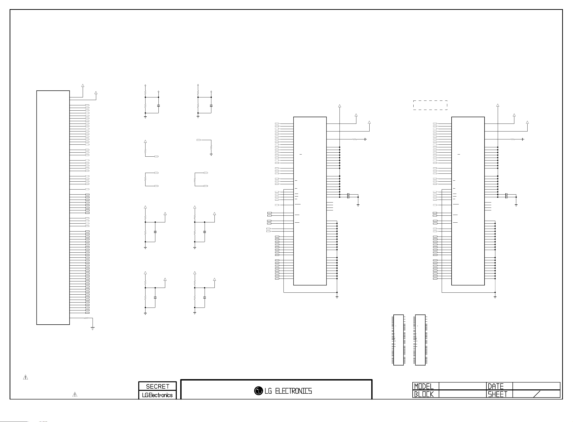
PAGE 5
Copyright ⓒ 2014 LG Electronics. Inc. All right reserved.
Only for training and service purposes
LGE Internal Use Only
IC101
LG1311
M1_DDR_VREF1
M1_DDR_VREF2
M1_DDR_U_CLKP
M1_DDR_U_CLKN
M1_DDR_D_CLKP
M1_DDR_D_CLKN
M1_DDR_RESET_N
M1_DDR_DQS_P0
M1_DDR_DQS_N0
M1_DDR_DQS_P1
M1_DDR_DQS_N1
M1_DDR_DQS_P2
M1_DDR_DQS_N2
M1_DDR_DQS_P3
M1_DDR_DQS_N3
M1_DDR_ZQCAL
M1_DDR_A0
M1_DDR_A1
M1_DDR_A2
M1_DDR_A3
M1_DDR_A4
M1_DDR_A5
M1_DDR_A6
M1_DDR_A7
M1_DDR_A8
M1_DDR_A9
M1_DDR_A10
M1_DDR_A11
M1_DDR_A12
M1_DDR_A13
M1_DDR_A14
M1_DDR_A15
M1_DDR_BA0
M1_DDR_BA1
M1_DDR_BA2
M1_DDR_CKE
M1_DDR_ODT
M1_DDR_RASN
M1_DDR_CASN
M1_DDR_WEN
M1_DDR_DM0
M1_DDR_DM1
M1_DDR_DM2
M1_DDR_DM3
M1_DDR_DQ0
M1_DDR_DQ1
M1_DDR_DQ2
M1_DDR_DQ3
M1_DDR_DQ4
M1_DDR_DQ5
M1_DDR_DQ6
M1_DDR_DQ7
M1_DDR_DQ8
M1_DDR_DQ9
M1_DDR_DQ10
M1_DDR_DQ11
M1_DDR_DQ12
M1_DDR_DQ13
M1_DDR_DQ14
M1_DDR_DQ15
M1_DDR_DQ16
M1_DDR_DQ17
M1_DDR_DQ18
M1_DDR_DQ19
M1_DDR_DQ20
M1_DDR_DQ21
M1_DDR_DQ22
M1_DDR_DQ23
M1_DDR_DQ24
M1_DDR_DQ25
M1_DDR_DQ26
M1_DDR_DQ27
M1_DDR_DQ28
M1_DDR_DQ29
M1_DDR_DQ30
M1_DDR_DQ31
VREF_M1_0
A2
Y1
M5
N5
K5
H5
T4
H4
R4
J5
T5
L5
U4
P4
P5
K4
R5
N4
G4
U5
L4
R3
R2
F3
F2
M4
F5
E4
F4
G5
J4
E2
E3
G2
G1
P2
P3
T2
T1
H1
E1
U1
P1
C2
K2
B3
J3
B1
K1
B2
K3
J2
D2
H3
C3
G3
D1
H2
D3
M2
V3
L3
W2
L1
W1
L2
W3
V2
N2
U3
M3
T3
N1
U2
N3
E5
R501
VREF_M1_1
M1_DDR_A0
M1_DDR_A1
M1_DDR_A2
M1_DDR_A3
M1_DDR_A4
M1_DDR_A5
M1_DDR_A6
M1_DDR_A7
M1_DDR_A8
M1_DDR_A9
M1_DDR_A10
M1_DDR_A11
M1_DDR_A12
M1_DDR_A13
M1_DDR_A14
M1_DDR_A15
M1_DDR_BA0
M1_DDR_BA1
M1_DDR_BA2
M1_U_CLK
M1_U_CLKN
M1_D_CLK
M1_D_CLKN
M1_DDR_CKE
M1_DDR_ODT
M1_DDR_RASN
M1_DDR_CASN
M1_DDR_WEN
M1_DDR_RESET_N
M1_DDR_DQS0
M1_DDR_DQS_N0
M1_DDR_DQS1
M1_DDR_DQS_N1
M1_DDR_DQS2
M1_DDR_DQS_N2
M1_DDR_DQS3
M1_DDR_DQS_N3
M1_DDR_DM0
M1_DDR_DM1
M1_DDR_DM2
M1_DDR_DM3
M1_DDR_DQ0
M1_DDR_DQ1
M1_DDR_DQ2
M1_DDR_DQ3
M1_DDR_DQ4
M1_DDR_DQ5
M1_DDR_DQ6
M1_DDR_DQ7
M1_DDR_DQ8
M1_DDR_DQ9
M1_DDR_DQ10
M1_DDR_DQ11
M1_DDR_DQ12
M1_DDR_DQ13
M1_DDR_DQ14
M1_DDR_DQ15
M1_DDR_DQ17
M1_DDR_DQ18
M1_DDR_DQ19
M1_DDR_DQ20
M1_DDR_DQ21
M1_DDR_DQ22
M1_DDR_DQ23
M1_DDR_DQ24
M1_DDR_DQ25
M1_DDR_DQ26
M1_DDR_DQ27
M1_DDR_DQ28
M1_DDR_DQ29
M1_DDR_DQ30
M1_DDR_DQ31
240
1%
+1.5V_DDR
+1.5V_DDR
+1.5V_DDR
+1.5V_DDR
VREF_M1_0
R508
1K
1%
R509
1K
1%
R502
10K
R503
100
M1_DDR_VREFCA
R504
1K
1%
R505
1K
1%
M1_DDR_VREFDQ
R506
1K
1%
R507
1K
1%
C501
0.1uF 16V
OPT
M1_DDR_RESET_N
M1_D_CLK
M1_D_CLKN
C502
0.1uF
16V
C503
0.1uF
16V
+1.5V_DDR
M1_DDR_CKE
+1.5V_DDR
+1.5V_DDR
VREF_M1_1
R515
1K
1%
R516
1K
1%
R510
100
M1_1_DDR_VREFCA
R511
1K
1%
C507
R512
1K
0.1uF
1%
16V
M1_1_DDR_VREFDQ
R513
1K
1%
C508
R514
1K
0.1uF
1%
16V
C506
0.1uF16V
OPT
R517
10K
M1_U_CLK
M1_U_CLKN
+1.5V_DDR
IC501
H5TQ4G63AFR-PBC
N3
M1_DDR_A0
M1_DDR_A1 M1_DDR_A1
M1_DDR_A2
M1_DDR_A3
M1_DDR_A4
M1_DDR_A5
M1_DDR_A6
M1_DDR_A7
M1_DDR_A8
M1_DDR_A9
M1_DDR_A10
M1_DDR_A11
M1_DDR_A12
M1_DDR_A13
M1_DDR_A14
M1_DDR_A15
M1_DDR_BA0
M1_DDR_BA1
M1_DDR_BA2
M1_D_CLK
M1_D_CLKN
M1_DDR_CKE
M1_DDR_ODT
M1_DDR_RASN
M1_DDR_CASN
M1_DDR_WEN
M1_DDR_RESET_N
M1_DDR_DQS0
M1_DDR_DQS_N0
M1_DDR_DQS1
M1_DDR_DQS_N1
M1_DDR_DM0
M1_DDR_DM1
M1_DDR_DQ0
M1_DDR_DQ1
M1_DDR_DQ2
M1_DDR_DQ3
M1_DDR_DQ4
M1_DDR_DQ5
M1_DDR_DQ6
M1_DDR_DQ7
M1_DDR_DQ8
M1_DDR_DQ9
M1_DDR_DQ10
M1_DDR_DQ11
M1_DDR_DQ12
M1_DDR_DQ13M1_DDR_DQ16
M1_DDR_DQ14
M1_DDR_DQ15
DDR3
A0
P7
4Gbit
A1
P3
DDR_512MB_HYNIX_1600_29n
A2
N2
A3
P8
A4
P2
A5
R8
A6
R2
A7
T8
A8
R3
A9
L7
A10/AP
R7
A11
N7
A12/BC
T3
A13
T7
A14
M7
A15
M2
BA0
N8
BA1
M3
BA2
J7
CK
K7
CK
K9
CKE
L2
CS
K1
ODT
J3
RAS
K3
CAS
L3
WE
T2
RESET
F3
DQSL
G3
DQSL
C7
DQSU
B7
DQSU
E7
DML
D3
DMU
E3
DQL0
F7
DQL1
F2
DQL2
F8
DQL3
H3
DQL4
H8
DQL5
G2
DQL6
H7
DQL7
D7
DQU0
C3
DQU1
C8
DQU2
C2
DQU3
A7
DQU4
A2
DQU5
B8
DQU6
A3
DQU7
VREFCA
VREFDQ
VDD_1
VDD_2
VDD_3
VDD_4
VDD_5
VDD_6
VDD_7
VDD_8
VDD_9
VDDQ_1
VDDQ_2
VDDQ_3
VDDQ_4
VDDQ_5
VDDQ_6
VDDQ_7
VDDQ_8
VDDQ_9
NC_1
NC_2
NC_3
NC_4
VSS_1
VSS_2
VSS_3
VSS_4
VSS_5
VSS_6
VSS_7
VSS_8
VSS_9
VSS_10
VSS_11
VSS_12
VSSQ_1
VSSQ_2
VSSQ_3
VSSQ_4
VSSQ_5
VSSQ_6
VSSQ_7
VSSQ_8
VSSQ_9
M8
H1
L8
ZQ
B2
D9
G7
K2
K8
N1
N9
R1
R9
A1
A8
C1
C9
D2
E9
F1
H2
H9
J1
J9
L1
L9
A9
B3
E1
G8
J2
J8
M1
M9
P1
P9
T1
T9
B1
B9
D1
D8
E2
E8
F9
G1
G9
M1_DDR_VREFCA
R518
+1.5V_DDR
OPT
C524
C525
OPT
0.1uF
0.1uF
16V
M1_DDR_VREFDQ
240
16V
DDR3 1.5V bypass Cap
: Place these caps near Memory
H5TQ2G63DFR-PBC
N3
A0
P7
A1
P3
A2
N2
A3
P8
A4
P2
A5
R8
A6
R2
A7
T8
A8
R3
A9
L7
A10/AP
R7
A11
N7
A12/BC
T3
A13
M7
NC_5
M2
BA0
N8
BA1
M3
BA2
J7
CK
K7
CK
K9
CKE
L2
CS
K1
ODT
J3
RAS
K3
CAS
L3
WE
T2
RESET
F3
DQSL
G3
DQSL
C7
DQSU
B7
DQSU
E7
DML
D3
DMU
E3
DQL0
F7
DQL1
F2
DQL2
F8
DQL3
H3
DQL4
H8
DQL5
G2
DQL6
H7
DQL7
D7
DQU0
C3
DQU1
C8
DQU2
C2
DQU3
A7
DQU4
A2
DQU5
B8
DQU6
A3
DQU7
IC501-*1
DDR_256MB_HYNIX_1600
VREFCA
VREFDQ
ZQ
VDD_1
VDD_2
VDD_3
VDD_4
VDD_5
VDD_6
VDD_7
VDD_8
VDD_9
VDDQ_1
VDDQ_2
VDDQ_3
VDDQ_4
VDDQ_5
VDDQ_6
VDDQ_7
VDDQ_8
VDDQ_9
NC_1
NC_2
NC_3
NC_4
NC_6
VSS_1
VSS_2
VSS_3
VSS_4
VSS_5
VSS_6
VSS_7
VSS_8
VSS_9
VSS_10
VSS_11
VSS_12
VSSQ_1
VSSQ_2
VSSQ_3
VSSQ_4
VSSQ_5
VSSQ_6
VSSQ_7
VSSQ_8
VSSQ_9
N3
M8
P7
P3
N2
H1
P8
P2
R8
L8
R2
T8
R3
B2
L7
D9
R7
G7
N7
K2
T3
K8
N1
M7
N9
R1
M2
R9
N8
M3
A1
J7
A8
K7
C1
K9
C9
D2
L2
E9
K1
F1
J3
H2
K3
H9
L3
J1
T2
J9
L1
L9
F3
T7
G3
C7
A9
B7
B3
E1
E7
G8
D3
J2
J8
E3
M1
F7
M9
F2
P1
F8
P9
H3
T1
H8
T9
G2
H7
B1
D7
B9
C3
D1
C8
D8
C2
E2
A7
E8
A2
F9
B8
G1
A3
G9
1_2Gbit : T7(NC_6)
4Gbit : T7(A14)
M1_DDR_A0
M1_DDR_A2
M1_DDR_A3
M1_DDR_A4
M1_DDR_A5
M1_DDR_A6
M1_DDR_A7
M1_DDR_A8
M1_DDR_A9
M1_DDR_A10
M1_DDR_A11
M1_DDR_A12
M1_DDR_A13
M1_DDR_A14
M1_DDR_A15
M1_DDR_BA0
M1_DDR_BA1
M1_DDR_BA2
M1_U_CLK
M1_U_CLKN
M1_DDR_CKE
M1_DDR_ODT
M1_DDR_RASN
M1_DDR_CASN
M1_DDR_WEN
M1_DDR_RESET_N
M1_DDR_DQS2
M1_DDR_DQS_N2
M1_DDR_DQS3
M1_DDR_DQS_N3
M1_DDR_DM2
M1_DDR_DM3
M1_DDR_DQ16
M1_DDR_DQ17
M1_DDR_DQ18
M1_DDR_DQ19
M1_DDR_DQ20
M1_DDR_DQ21
M1_DDR_DQ22
M1_DDR_DQ23
M1_DDR_DQ24
M1_DDR_DQ25
M1_DDR_DQ26
M1_DDR_DQ27
M1_DDR_DQ28
M1_DDR_DQ29
M1_DDR_DQ30
M1_DDR_DQ31
IC502-*1
H5TQ2G63DFR-PBC
DDR_256MB_HYNIX_1600
M8
A0
VREFCA
A1
A2
H1
A3
VREFDQ
A4
A5
L8
A6
ZQ
A7
A8
B2
A9
VDD_1
D9
A10/AP
VDD_2
G7
A11
VDD_3
K2
A12/BC
VDD_4
K8
A13
VDD_5
N1
VDD_6
N9
NC_5
VDD_7
R1
VDD_8
R9
BA0
VDD_9
BA1
BA2
A1
VDDQ_1
A8
CK
VDDQ_2
C1
CK
VDDQ_3
C9
CKE
VDDQ_4
D2
VDDQ_5
E9
CS
VDDQ_6
F1
ODT
VDDQ_7
H2
RAS
VDDQ_8
H9
CAS
VDDQ_9
WE
J1
NC_1
J9
RESET
NC_2
L1
NC_3
L9
NC_4
T7
DQSL
NC_6
DQSL
A9
DQSU
VSS_1
B3
DQSU
VSS_2
E1
VSS_3
G8
DML
VSS_4
J2
DMU
VSS_5
J8
VSS_6
M1
DQL0
VSS_7
M9
DQL1
VSS_8
P1
DQL2
VSS_9
P9
DQL3
VSS_10
T1
DQL4
VSS_11
T9
DQL5
VSS_12
DQL6
DQL7
B1
VSSQ_1
B9
DQU0
VSSQ_2
D1
DQU1
VSSQ_3
D8
DQU2
VSSQ_4
E2
DQU3
VSSQ_5
E8
DQU4
VSSQ_6
F9
DQU5
VSSQ_7
G1
DQU6
VSSQ_8
G9
DQU7
VSSQ_9
IC502
H5TQ4G63AFR-PBC
N3
DDR3
A0
P7
4Gbit
A1
P3
DDR_512MB_HYNIX_1600_29n
A2
N2
A3
P8
A4
P2
A5
R8
A6
R2
A7
T8
A8
R3
A9
L7
A10/AP
R7
A11
N7
A12/BC
T3
A13
T7
A14
M7
A15
M2
BA0
N8
BA1
M3
BA2
J7
CK
K7
CK
K9
CKE
L2
CS
K1
ODT
J3
RAS
K3
CAS
L3
WE
T2
RESET
F3
DQSL
G3
DQSL
C7
DQSU
B7
DQSU
E7
DML
D3
DMU
E3
DQL0
F7
DQL1
F2
DQL2
F8
DQL3
H3
DQL4
H8
DQL5
G2
DQL6
H7
DQL7
D7
DQU0
C3
DQU1
C8
DQU2
C2
DQU3
A7
DQU4
A2
DQU5
B8
DQU6
A3
DQU7
VREFCA
VREFDQ
VDD_1
VDD_2
VDD_3
VDD_4
VDD_5
VDD_6
VDD_7
VDD_8
VDD_9
VDDQ_1
VDDQ_2
VDDQ_3
VDDQ_4
VDDQ_5
VDDQ_6
VDDQ_7
VDDQ_8
VDDQ_9
NC_1
NC_2
NC_3
NC_4
VSS_1
VSS_2
VSS_3
VSS_4
VSS_5
VSS_6
VSS_7
VSS_8
VSS_9
VSS_10
VSS_11
VSS_12
VSSQ_1
VSSQ_2
VSSQ_3
VSSQ_4
VSSQ_5
VSSQ_6
VSSQ_7
VSSQ_8
VSSQ_9
ZQ
+1.5V_DDR
M8
H1
L8
B2
D9
G7
K2
K8
N1
N9
R1
R9
A1
A8
C1
C9
D2
E9
F1
H2
H9
J1
J9
L1
L9
A9
B3
E1
G8
J2
J8
M1
M9
P1
P9
T1
T9
B1
B9
D1
D8
E2
E8
F9
G1
G9
M1_1_DDR_VREFCA
R519
+1.5V_DDR
0.1uF
C540
0.1uF
C541
M1_1_DDR_VREFDQ
240
16V
16V
DDR3 1.5V bypass Cap
: Place these caps near Memory
THE SYMBOL MARK OF THIS SCHEMETIC DIAGRAM INCORPORATES
SPECIAL FEATURES IMPORTANT FOR PROTECTION FROM X-RADIATION.
FIRE AND ELECTRICAL SHOCK HAZARDS, WHEN SERVICING IF IS
ESSENTIAL THAT ONLY MANUFACTURES SPECIFIED PARTS BE USED FOR
THE CRITICAL COMPONENTS IN THE SYMBOL MARK OF THE SCHEMETIC.
LS55A
M14 DDR3-M1
2013.10.21
5
31
Page 22
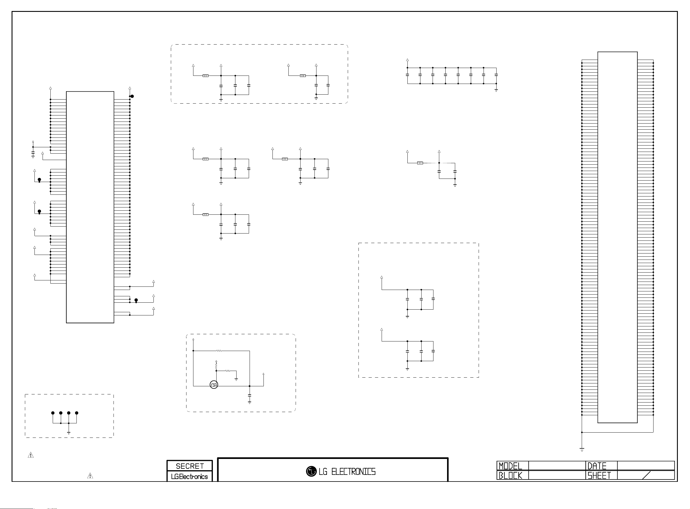
PAGE 6
Copyright ⓒ 2014 LG Electronics. Inc. All right reserved.
Only for training and service purposes
LGE Internal Use Only
VDD3V3_HDMI
AVDD33
C637
0.1uF
16V
+1.5V_DDR
TP5207
+1.5V_DDR
TP5208
AVDD25_C4TX
AVDD25
AVDD25_AUD
GND JIG POINT
DVDD33
JP601
AA23
AC12
AC13
AC14
AC15
AC11
AF22
AA11
AC18
AC19
AC20
AC21
AC22
AC23
AC17
AB23
L18
L21
L22
L23
M23
T11
Y23
P23
R23
T23
U23
V23
F10
F11
F12
F13
F14
F15
F16
F17
V11
W11
Y11
G19
H19
H20
F9
G6
H6
J6
K6
L6
M6
N6
P6
R6
JP602
IC101
LG1311
DVDD33_1
DVDD33_2
DVDD33_3
DVDD33_4
DVDD33_5
DVDD33_6
DVDD33_7
DVDD33_8
DVDD33_9
DVDD33_10
DVDD33_11
DVDD33_12
AVDD33_BT_USB
AVDD33_USB_1
AVDD33_USB_2
AVDD33_HDMI_1
AVDD33_HDMI_2
AVDD33_HDMI_3
AVDD33_CVBS
DVDD15_M0_1
DVDD15_M0_2
DVDD15_M0_3
DVDD15_M0_4
DVDD15_M0_5
DVDD15_M0_6
DVDD15_M0_7
DVDD15_M0_8
DVDD15_M0_9
DVDD15_M1_1
DVDD15_M1_2
DVDD15_M1_3
DVDD15_M1_4
DVDD15_M1_5
DVDD15_M1_6
DVDD15_M1_7
DVDD15_M1_8
DVDD15_M1_9
AVDD25_C4TX_1
AVDD25_C4TX_2
AVDD25_C4TX_3
AVDD25_C4TX_4
AVDD25_COMP_1
AVDD25_COMP_2
AVDD25_CVBS_1
AVDD25_CVBS_2
AVDD25_DMD
AVDD25_AAD
DVDD25_XTAL
AVDD25_DR3PLL
SP_VQPS
AVDD25_AUD
AVDD25_APLL
JP604
JP603
DVDD11_1
DVDD11_2
DVDD11_3
DVDD11_4
DVDD11_5
DVDD11_6
DVDD11_7
DVDD11_8
DVDD11_9
DVDD11_10
DVDD11_11
DVDD11_12
DVDD11_13
DVDD11_14
DVDD11_15
DVDD11_16
DVDD11_17
DVDD11_18
DVDD11_19
DVDD11_20
DVDD11_21
DVDD11_22
DVDD11_23
DVDD11_24
DVDD11_25
DVDD11_26
DVDD11_27
DVDD11_28
DVDD11_29
DVDD11_30
DVDD11_31
DVDD11_32
DVDD11_33
DVDD11_34
DVDD11_35
DVDD11_36
DVDD11_37
DVDD11_38
DVDD11_39
DVDD11_40
DVDD11_41
DVDD11_42
DVDD11_43
DVDD11_44
DVDD11_45
DVDD11_46
DVDD11_47
DVDD11_48
DVDD11_49
DVDD11_50
DVDD11_51
AVDD11_APLL
AVDD11_COMP_LLPLL
AVDD11_C4TX_1
AVDD11_C4TX_2
AVDD11_C4TX_3
AVDD11_C4TX_4
DVDD11_XTAL
DVDD11_DR3PLL
DVDD11_CVBSPLL
AVDD11_DMD_1
AVDD11_DMD_2
DVDD18_EMMC_1
DVDD18_EMMC_2
+1.1V_VDD
M20
M21
N13
N14
N15
N16
N17
N18
P20
P21
R13
R14
R15
R16
R17
R18
R19
R20
R21
T13
T20
T21
U14
U15
U16
U17
U18
U19
U20
U21
V13
V20
V21
W13
W14
W15
W16
W17
W18
W19
Y13
Y20
Y21
AA13
AA14
AA15
AA17
AA18
AA19
AA20
AA21
AB21
AB19
V12
W12
Y12
AA12
G18
H18
AF23
AF24
AF25
L26
M26
TP5209
+1.1V_VDD
AVDD11_DMD
TP5210
DVDD18_EMMC
+3.3V_Bypass Cap
+3.3V_NORMAL
PZ1608U121-2R0TF
L601
DVDD33
C601
4.7uF
10V
C604
4.7uF
10V
C607
0.1uF
16V
+2.5V_Bypass Cap
+2.5V_NORMAL
PZ1608U121-2R0TF
+2.5V_NORMAL
PZ1608U121-2R0TF
HDMI LEAKAGE Workaround in MTK A2(A0) (Default= with HDMI_LEAKAGE)
+3.3V_NORMAL
L602
4.7uF
AVDD25_AUD
L603
4.7uF
D
NTR4501NT1G
AVDD25
C602
10V
C603
10V
R602
0
1/16W
5%
R601
10K
G
Q601
4.7uF
4.7uF
OPT
PANEL_VCC
13K
S
C605
C606
R603
C608
0.1uF
16V
10V
C609
0.1uF
16V
10V
VDD3V3_HDMI
C635
0.1uF
16V
+3.3V_NORMAL
+2.5V_NORMAL
PZ1608U121-2R0TF
PZ1608U121-2R0TF
AFE 3CH Power
AVDD25_C4TX
L604
C610
4.7uF
10V
L606
4.7uF
C613
4.7uF
C614
10V
AVDD33
10V
C616
0.1uF
16V
C615
0.1uF
16V
+1.1V_VDD
C617
4.7uF
10V
+1.1V_VDD
+1.5V_Bypass Cap
+1.5V_DDR
+1.5V_DDR
+1.1V_Bypass Cap
C619
C618
4.7uF
10V
L607
PZ1608U121-2R0TF
OPT
C629
22uF
10V
OPT
C630
22uF
10V
4.7uF
10V
AVDD11_DMD
C622
4.7uF
10V
C631
0.1uF
16V
C632
0.1uF
16V
C620
4.7uF
C633
0.1uF
16V
C634
0.1uF
16V
10V
C625
0.1uF
C623
4.7uF
16V
IC101
LG1311
GND_1
GND_2
GND_3
GND_4
GND_5
GND_6
GND_7
GND_8
GND_9
GND_10
GND_11
GND_12
GND_13
GND_14
GND_15
GND_16
GND_17
GND_18
GND_19
GND_20
GND_21
GND_22
GND_23
GND_24
GND_25
GND_26
GND_27
GND_28
GND_29
GND_30
GND_31
GND_32
GND_33
GND_34
GND_35
GND_36
GND_37
GND_38
GND_39
GND_40
GND_41
GND_42
GND_43
GND_44
GND_45
GND_46
GND_47
GND_48
GND_49
GND_50
GND_51
GND_52
GND_53
GND_54
GND_55
GND_56
GND_57
GND_58
GND_59
GND_60
GND_61
GND_62
GND_63
GND_64
GND_65
GND_66
GND_67
GND_68
GND_69
GND_70
GND_71
GND_72
GND_73
GND_74
GND_75
GND_76
GND_77
GND_78
GND_79
GND_80
GND_81
GND_82
GND_83
GND_84
GND_85
GND_86
GND_87
GND_88
GND_89
GND_90
GND_91
GND_92
GND_93
GND_94
GND_95
GND_96
GND_97
GND_98
GND_99
GND_100
GND_101
GND_102
GND_103
GND_104
GND_105
GND_106
GND_107
GND_108
GND_109
GND_110
GND_111
GND_112
GND_113
@optio
GND_114
GND_115
GND_116
GND_117
GND_118
GND_119
GND_120
GND_121
GND_122
GND_123
GND_124
GND_125
GND_126
GND_127
GND_128
GND_129
GND_130
GND_131
GND_132
GND_133
GND_134
GND_135
GND_136
GND_137
GND_138
GND_139
GND_140
GND_141
GND_142
GND_143
GND_144
GND_145
GND_146
GND_147
GND_148
GND_149
GND_150
GND_151
GND_152
GND_153
GND_154
GND_155
GND_156
GND_157
GND_158
GND_159
GND_160
GND_161
GND_162
GND_163
GND_164
GND_165
GND_166
GND_167
GND_168
GND_169
GND_170
GND_171
GND_172
GND_173
GND_174
GND_175
GND_176
GND_177
GND_178
GND_179
GND_180
GND_181
GND_182
GND_183
GND_184
GND_185
GND_186
GND_187
GND_188
GND_189
GND_190
GND_191
GND_192
GND_193
GND_194
GND_195
GND_196
GND_197
GND_198
GND_199
GND_200
GND_201
GND_202
GND_203
GND_204
GND_205
GND_206
GND_207
GND_208
GND_209
GND_210
GND_211
GND_212
GND_213
GND_214
GND_215
GND_216
GND_217
GND_218
GND_219
GND_220
GND_221
GND_222
GND_223
GND_224
GND_225
GND_226
P19
P22
P26
P30
R7
R8
R11
R12
R22
R26
R27
T6
T7
T8
T12
T14
T15
T16
T17
T18
T19
T22
T26
T27
U6
U7
U8
U11
U12
U13
U22
U26
V4
V5
V6
V7
V8
V14
V15
V16
V17
V18
V19
V22
V26
V30
V31
W4
W8
W20
W21
W22
W23
W26
W27
Y2
Y3
Y4
Y8
Y14
Y15
Y16
Y17
Y18
Y19
Y22
Y26
AA8
AA16
AA22
AA26
AB11
AB12
AB13
AB14
AB15
AB16
AB17
AB18
AB20
AB22
AB26
AB30
AB31
AC16
AC26
AD26
AE26
AF6
AF8
AF9
AF10
AF11
AF12
AF13
AF14
AF15
AF16
AF17
AF18
AF19
AF20
AF21
AF26
AG20
AG25
AG31
AH25
AJ25
AK9
AK25
AL9
AL15
B22
B24
C22
C23
C626
C627
0.1uF
C628
0.1uF
16V
16V
0.1uF
10V
16V
C24
D4
D5
D6
D20
D21
E6
E20
E21
F6
F7
F8
F18
F19
F20
F21
G7
G8
G9
G10
G11
G12
G13
G14
G15
G16
G17
G20
G21
G22
G23
G24
G25
G26
G27
H7
H8
H9
H10
H11
H12
H13
H14
H15
H16
H17
H21
H22
H23
H24
H25
H26
H27
H31
J7
J8
J26
J27
K7
K8
K26
K27
L7
L8
L11
L12
L13
L14
L15
L16
L17
L19
L20
L27
M7
M8
M11
M12
M13
M14
M15
M16
M17
M18
M19
M22
M27
N7
N8
N11
N12
N19
N20
N21
N22
N23
N26
N27
N30
P7
P8
P11
P12
P13
P14
P15
P16
P17
P18
THE SYMBOL MARK OF THIS SCHEMETIC DIAGRAM INCORPORATES
SPECIAL FEATURES IMPORTANT FOR PROTECTION FROM X-RADIATION.
FIRE AND ELECTRICAL SHOCK HAZARDS, WHEN SERVICING IF IS
ESSENTIAL THAT ONLY MANUFACTURES SPECIFIED PARTS BE USED FOR
THE CRITICAL COMPONENTS IN THE SYMBOL MARK OF THE SCHEMETIC.
11/05/31
LS55A
VCC & GND
2013.10.21
6
31
Page 23
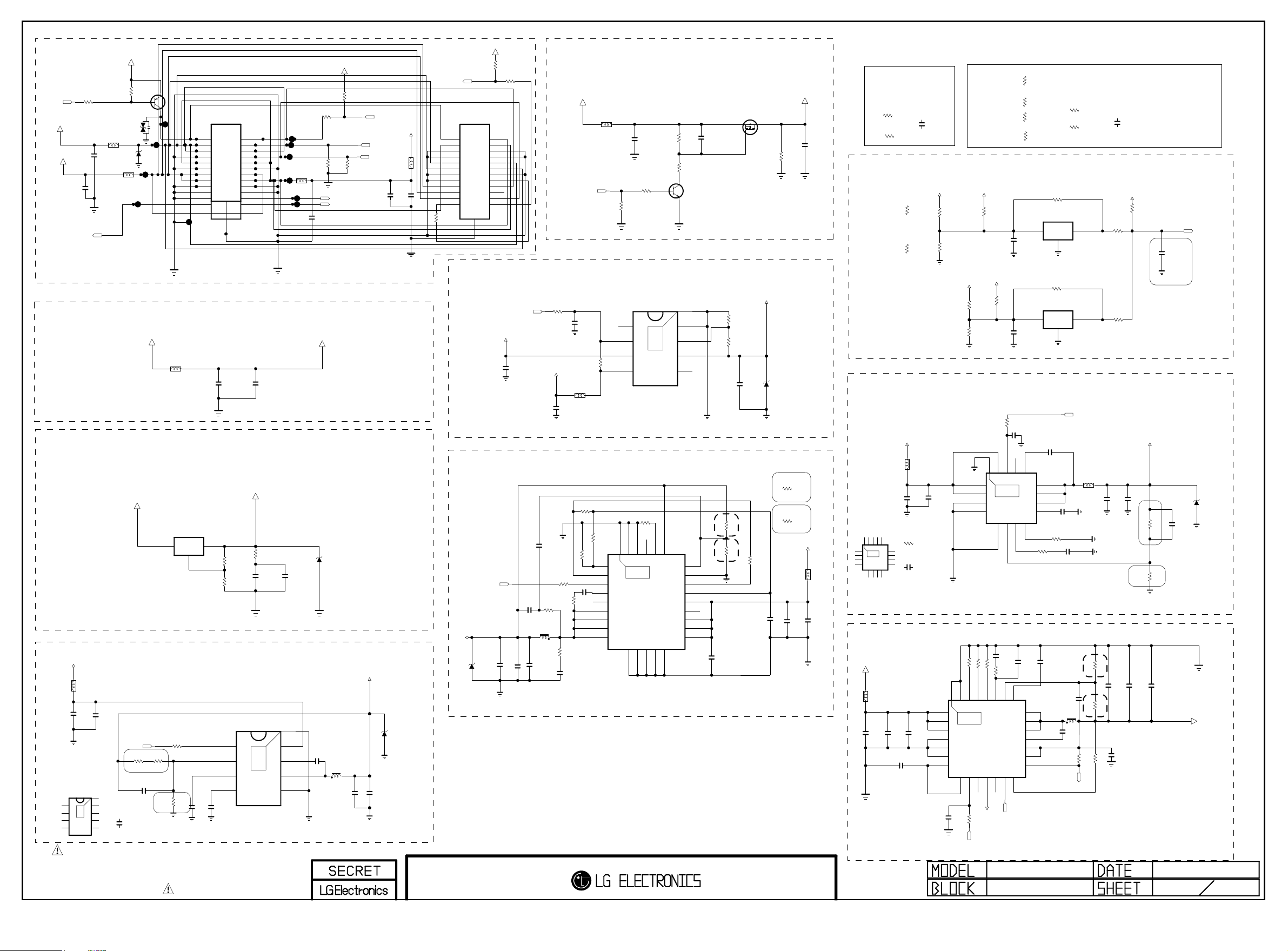
+3.5V_ST
Copyright ⓒ 2014 LG Electronics. Inc. All right reserved.
Only for training and service purposes
LGE Internal Use Only
+3.3V_NORMAL
RL_ON
+3.5V_ST
+12V
C2306
0.1uF
L/DIM0_MOSI
R2301
R2300
10K
50V
10K
MMBT3906(NXP)
VA23001
AMOTECH CO., LTD.
L2304
UBW2012-121F
C2307
0.1uF
16V
UBW2012-121F
L2303
5.6V
Q2300
2
5V
ZD2303
14.02.06
1
3
POWER_WAFER_18PIN
PWR ON
3.5V
3.5V
GND
24V
GND
12V
12V
GND
GND
GND
L/DIM0_MOSI
DEV_POWER_WAFER_24PIN
P2300
SMAW200-H18S5
1
1
3
3
5
5
7
7
10
9
9
10
11
12
12
11
13
14
13
14
15
16
16
15
17
18
18
17
20
19
21
22
19
23
24
25
.
SMAW200-H24S2
P2301
INV ON
2
2
PDIM#1
4
4
3.5V
6
6
PDIM#2
8
8
24V
GND
12V
24V
GND
GND
L/DIMO_VS
L/DIM0_SCLK
L2306
UBW2012-121F
C2316
0.1uF
50V
R2309
100
R2354
4.7K
OPT
L/DIM0_VS
L/DIM0_SCLK
R2310
1K
R2355
4.7K
OPT
OPT
PWM_DIM
PWM_DIM2
C2358
0.1uF
INV_CTL
50V
C2359
10uF
L2312
35V
+24V
UBW2012-121F
+3.3V - eMMC 4.41(LG1311-A0)
+3.3V_NORMAL
L2302
PZ1608U121-2R0TF
C2305
0.1uF
16V
C2300
22uF
10V
3.3V_EMMC
+1.8V - eMMC 4.51(LG1311-B0)
+3.3V_NORMAL
IC2306
AZ1117EH-ADJTRG1
OUTIN
ADJ/GND
+12V
+3.3V_NORMAL
L2300
PZ1608U121-2R0TF
C2302
C2303
10uF
0.1uF
16V
16V
R23 03
68K
1/1 6W
1%
R2304
10K
R1
R2
R23 05
22K
1/1 6W
1%
POWER_ON/OFF1
R2302
5.1K
1/16W
1%
C2304
100pF
EN
VFB
VREG5
SS
3.3V_DCDC_TI
IC2300-*1
TPS54327DDAR
1
2
3
4
THERMAL
[EP]GND
VIN
8
VBST
9
7
SW
6
GND
5
3.3V_DCDC_RHOM
3.3V_DCDC_TI
C2312-*1
3300pF
50V
50V
THE SYMBOL MARK OF THIS SCHEMETIC DIAGRAM INCORPORATES
SPECIAL FEATURES IMPORTANT FOR PROTECTION FROM X-RADIATION.
FIRE AND ELECTRICAL SHOCK HAZARDS, WHEN SERVICING IF IS
ESSENTIAL THAT ONLY MANUFACTURES SPECIFIED PARTS BE USED FOR
THE CRITICAL COMPONENTS IN THE SYMBOL MARK OF THE SCHEMETIC.
DVDD18_EMMC
R2347
1
75
1%
1/16W
R2357
C2301
10uF
33
C2310
1uF
10V
1%
1/16W
VREG
C2312
2200pF
50V
3.3V_DCDC_RHOM
R2358
BD9D320EFJ
EN
1
FB
2
3
3.3V_DCDC_RHOM
SS
4
IC2300
THERMAL
3A
10V
[EP]FIN
VIN
8
BOOT
9
7
SW
6
GND
5
Vout=0.765*(1+R1/R2)
C2308
10uF
10V
OPT
16V
0.1uF
C2313
2.5V
D2302
L2301
2uH
C2314
22uF
10V
+3.3V_NORMAL
C2315
22uF
10V
5V
ZD2300
+3.3V_NORMAL
PANEL_POWER
R8813
4.7K
OPT
OPT
R8812
ERROR_OUT
100
+12V
POWER_WAFER_24PIN_LS75A
P2302
0
PWR ON
3.5V
3.5V
R8811
24V
GND
GND
GND
GND
GND
12V
12V
GND
14.02.06
SMAW200-H24S5
1
2
3
4
5
6
7
8
10
9
11
12
13
14
15
16
17
18
20
19
21
22
23
24
25
GND
24V
24V
GND
GND
3.5V
3.5V
GND
GND
INV ON
FLOATING
PDIM
ERROR_OUT
PANEL_CTL
L2313
UBW2012-121F
R8814
10K
+2.5V
POWER_ON/OFF2_1
+3.3V_NORMAL
C2327
0.1uF
16V
R2312
10K
16V
+5V_NORMAL
PZ1608U121-2R0TF
C2337
1uF
25V
14.02.21
L8703
14.02.21
AP2132MP-2.5TRG1
C2346
0.1uF
READY
R8845
0
PG
EN
VIN
VCTRL
Vout=0.6*(1+R1/R2)
+1.1V_CORE
R2311
10K
1%
C2321
1000pF
50V
C2320
0.1uF
16V
C2319
22uF
10V
L2305
1uH
R2307 1K
R2306
2K
1/16W
5%
R2308
3.3
1/10W
C2322
470pF
50V
POWER_ON/OFF2_3
+1.1V_VDD
C2317
22uF
10V
OPT
2.5V
ZD2301
C2318
22uF
10V
SoC A0/A1 : 1.22V(R1/R2=10.7K,10.5K)
SoC B0 : 1.12V(R1/R2=9.1K10.7K)(1309016)
POWER UP SEQUENCE
3.3V->2.5V->1.5V/1.1V->5V
91K
1/1 6W
R23 15
27K
R23 13
PGOOD
VBST
NC_1
SW_1
SW_2
SW_3
SW_4
RF
1
2
EN
3
4
5
6
7
8
9
[EP]
THERMAL
TPS53513RVER
10
PGND_111PGND_212PGND_313PGND_414PGND_5
R2351
5%
1%
0.1uF
C2323
4.7
1/1 6W
16V
Vout=0.6*(1+R1/R2)
C2331
0.1uF
50V
R2314
10K
IC2302
1
2
3
4
EAN61387601
R2316
39K
1/16W
5%
29
IC2301
8A
2A
R2318
9
THERMAL
TRIP26NC_327GND128GND2
R2317
18K
B
24VO25
100K
8
7
6
5
14.02.06
C
Q2301
MMBT3904(NXP)
E
[EP]
GND
ADJ
VOUT
NC
FB
23
GND
22
MODE
21
VREG
20
VDD
19
NC_2
18
VIN_3
17
VIN_2
16
VIN_1
15
C2333
10uF
16V
R1
R2
R2321
R23 22
R2319
9.1K
R2320
10.7K
CORE_V_B0
C2325
2200pF
50V
Q2302
DMP2130L
S
1.2K
R2
R1
3.9 K
C2357
10uF
10V
1/16W
1%
CORE_V_B0
1/16W
1%
1%
D
G
+2.5V_NORMAL
OPT
20K
R2323
1/16W
PANEL_VCC
R2346
3.3K
LVDS_DISCHARGE
5V
ZD2304
CORE_V_A0/A1
R2319-*1
10.7K
1/16W
1%
CORE_V_A0/A1
R2320-*1
10.5K
1/16W
1%
L2307
C2326
C2328
1uF
10uF
10V
16V
PAGE 8
R2327-*1
P_DET_BOTH_12_24V
P_DET_BOTH_12_24V
P_DET_BOTH_12_24V
P_DET_BOTH_12_24V
C2347
0.1uF
50V
R2349-*1
100
P_DET_BOTH_24_3.5V
R2336-*1
100K
P_DET_BOTH_24_3.5V
C2356-*1
0.1uF
50V
P_DET_BOTH_24_3.5V
Power_DET
P_DET_BOTH_12_3.5V
P_DET_BOTH_12_3.5V
+12V
R2325-*1
2.7K
1%
R2326-*1
1.2K
1%
P_DET_BOTH_24_3.5V
P_DET_BOTH_24_3.5V
P_DET_ONLY_12V
R2325
2.7K
1%
P_DET_ONLY_12V
R2326
1.2K
1%
+24V
+3.5V_ST
R2327
8.2K
R2328
1.5K
1%
READY
R2330
0
5%
+3.5V_ST
DDR MAIN 1.5V
+3.5V_ST
L2308
R1
R2
+12V
1.5V_DCDC_TI
EP[GND]
VIN_1
1
VIN_2
2
GND_1
3
GND_2
4
THERMAL
17
IC2303-*1
TPS54319TRE
5
AGND
BOOT14PWRGD15EN16VIN_3
13
7
8
COMP
RT/CLK6VSENSE
PH_3
12
PH_2
11
PH_1
10
SS/TR
9
1.5V_DCDC_TI
1.5V_DCDC_TI
C2339
10uF
10V
R2329-*1
15K
1/16W
5%
C2344-*1
4700pF50V
C2340
0.1uF
16V
PVIN_1
PVIN_2
PGND_1
PGND_2
[EP]FIN
1
2
3
4
1.5V_DCDC_RHOM
AGND8MODE
Vout=0.8*(1+R1/R2)
C2332
10uF
16V
+5.0V normal & USB
+24V
R23 35 16 K 1 %
R23 40 16 K 1 %
R23 41150 K 1%
L2310
120-ohm
C2309
10uF
35V
OPT
C2311
10uF
35V
C2329
0.1uF
50V
1uF
25V
C23 24
[EP]
RSET2
AGND
27
28
VIN_1
1
THERMAL
VIN_2
2
VIN_3
PGND_1
PGND_2
PGND_3
C2330
0.0068uF
50V
29
3
IC2304
4
SN1302001(TPS65286RHDR)
5
6
V7V
7
MODE/SYNC
6A
9EN10
8
10K
R2339
POWER_ON/OFF2_4
COMP25RLIM26RSET1
SW_EN213SW_EN1
SW_OUT211SW_OUT1
+5V_USB_3
12
8.2K
R2328-*1
1.5K
1%
R2325-*2
2.7K
1%
R2326-*2
1.2K
1%
VDD
C2355
0.1uF
16V
P_DET_BOTH_12_3.5V
R2348
0
READY
VDD
C2356
0.1uF
50V
P_DET_BOTH_12_3.5V
10K
C2353
R2324
0.1uF
16V
1.5V_DCDC_TI
BOOT14PGD15EN16AVIN
13
12
THERMAL
11
17
3A
10
IC2303
BD9A300MUV
5
7
6
FB
ITH
9
1.5V_DCDC_RHOM
3A
C2334
OPT
2200pF
C2335
50V
100pF
50V
R2342
10K
22SS23FB24
LX_3
21
LX_2
20
LX_1
19
BST
18
SW_IN2
17
SW_IN1
16
NFAULT1
15
14
NFAULT2
USB_CTL3
LS55A
POWER
P_DET_BOTH_12_24V
R2336-*2
100K
C2356-*2
0.1uF
50V
P_DET_BOTH_12_24V
+3.5V_ST
R2350
100
R2349
100
P_DET_BOTH_12_3.5V
C2345
C2349
22uF
22uF
10V
10V
6.8K
1/16W
R2345
C2348
22uF
10V
51K
1/16W
R2352
C2350
1uF
5%
10V
100K
1/16W
R1
R2
P_DET_BOTH_12_24V
R2337
100K
IC2307
BD48K28G
3
1
R2336
100K
IC2308
BD48K28G
3
1
C2341
0.1uF
16V
SW_3
SW_2
SW_1
SS
0.01uF
R2331
330K1/16W 5%
R2329
8.2K
1/16W1%
C2336
0.047uF
25V
R2349-*2
100
VOUT
2
GND
VOUT
2
GND
POWER_ON/OFF2_2
NR5040T2R2N
L2309
2.2uH
C2342
50V
C2344
2700pF50V
1.5V_DCDC_RHOM
C2343
82pF
50V
L2311
4.7uH
C2338
0.047uF
25V
5%
100K
R2344
1/16W
/USB_OCD3
R2
1%
R1
1%
R2353
Vout=0.6*(1+R1/R2)
5V:R1-36K, R2-4.8K
5.1V:R1-51K, R2-6.8K
R2338
10K
OPT
C2365
0.1uF
16V
not to RESET at 8kV ESD
ST_3.5V-->3.5V
+1.5V_DDR
1%
16K
R23 32
1/1 6W
1.5V_DCDC_TI
1%
18K
R23 33
1/1 6W
C2352
C2351
10uF
22uF
10V
10V
2013.03.22
POWER_DET
24V-->3.48V
12V-->3.58V
2.5V
ZD2302
OPT
C2354
100pF
50V
+5V_NORMAL
8
31
Page 24

+3.5V_ST
Copyright ⓒ 2014 LG Electronics. Inc. All right reserved.
Only for training and service purposes
LGE Internal Use Only
Q1103
PMV48XP
D
S
SII9489
BODY_SHIELD
20
19
HOT_PLUG_DETECT
18
VDD[+5V]
HDMI_1
RSD-105156-100
JK1101
5V_DET_HDMI
5V_HDMI
R1101
1.8K
R1102
3.3K
BODY_SHIELD
HDMI_2
RSD-105156-100
17
DDC/CEC_GND
16
SDA
15
SCL
14
RESERVED
13
CEC
12
TMDS_CLK-
11
TMDS_CLK_SHIELD
10
TMDS_CLK+
9
TMDS_DATA0-
8
TMDS_DATA0_SHIELD
7
TMDS_DATA0+
6
TMDS_DATA1-
5
TMDS_DATA1_SHIELD
4
TMDS_DATA1+
3
TMDS_DATA2-
2
TMDS_DATA2_SHIELD
1
TMDS_DATA2+
20
19
HOT_PLUG_DETECT
18
VDD[+5V]
17
DDC/CEC_GND
16
SDA
15
SCL
14
RESERVED
13
CEC
12
TMDS_CLK-
11
TMDS_CLK_SHIELD
10
TMDS_CLK+
9
TMDS_DATA0-
8
TMDS_DATA0_SHIELD
7
TMDS_DATA0+
6
TMDS_DATA1-
5
TMDS_DATA1_SHIELD
4
TMDS_DATA1+
3
TMDS_DATA2-
2
TMDS_DATA2_SHIELD
1
TMDS_DATA2+
JK1501
5V_HDMI
1 8
2 7
3 6
4 5
9
1 8
2 7
3 6
4 5
9
+5V_ST
A2CA1
KDS184
D1106
85V
D1105
MMBD301LT1G
30V
C1121
0.1uF
50V
1 8
2 7
3 6
4 5
1
2 7
3 6
4 5
5V_HDMI_2
R1506
1.8K
R1507
3.3K
JP1104
JP1103
9
9
5V_DET_HDMI_2
/DIGITAL_DPM_CTRL
5V_HDMI
5.5V
VA23007
CEC_REMOTE
D1101
RCLAMP0544T.TCT
6.5VTO11.0V
D1102
RCLAMP0544T.TCT
6.5VTO11.0V
0.HDMI_1
R1123
4.7K
R11 24
4.7K
5V_HDMI_2
5.5V
JP1502
JP1501
8
VA23008
CEC_REMOTE
D1502
RCLAMP0544T.TCT
6.5VTO11.0V
D1503
RCLAMP0544T.TCT
6.5VTO11.0V
5V_HDMI_2
HDMI_HPD
HDMI_SDA
HDMI_SCL
+3.5V_ST
10K
R1508
C1503
0.1uF
HDMI_2_HPD
+5V_ST
A2CA1
KDS184
D1505
85V
D1504
MMBD301LT1G
30V
C1502
0.1uF
50V
+3.5V_ST
10K
R1167
VA1102
C1153
20V
0.1uF
25V
HDMI_SDA
HDMI_SCL
R0XCN
R0XCP
R0X0N
R0X0P
R0X1N
R0X1P
R0X2N
R0X2P
VA1501
20V
25V
HDMI_2_SDA
HDMI_2_SCL
R2XCN
R2XCP
R2X0N
R2X0P
R2X1N
R2X1P
R2X2N
R2X2P
2.HDMI_2
DET_HDMI_2
R1509
4.7K
R15 10 4.7K
R1119
470K
DET_HDMI
2.DP
3.DVI
M100 ESD
MDS62110209
M101 ESD
MDS62110215
M102
MDS62110209
DP_RXC-
DP_RXC+
DP_RX0DP_RX0+
DP_RX1-
DP_RX1+
DP_RX2DP_RX2+
ESD
HDMI_2_SDA
HDMI_2_SCL
C1104
G
2.2uF
R1161
100K
C1105
VDDA_33_S
R3XCN
R3XCP
R3X0N
R3X0P
R3X1N
R3X1P
R3X2N
R3X2P
M103 ESD
MDS62110209
M104 ESD
MDS62110209
M105 ESD
MDS62110215
16V
C1107
22uF
22uF
10V
10V
0.1uF
16V
C1108
VDDA_12_S
VDD_12_S
SMD Bottom
M106 ESD
M107 ESD
M108 ESD
C1106
2.2uF
16V
C1109
22uF
10V
0.1uF
10V
10uF
C1112
C1110
MDS62110215
MDS62110209
MDS62110215
R1120
1.HDMI_2
16V
THE SYMBOL MARK OF THIS SCHEMETIC DIAGRAM INCORPORATES
SPECIAL FEATURES IMPORTANT FOR PROTECTION FROM X-RADIATION.
FIRE AND ELECTRICAL SHOCK HAZARDS, WHEN SERVICING IF IS
ESSENTIAL THAT ONLY MANUFACTURES SPECIFIED PARTS BE USED FOR
THE CRITICAL COMPONENTS IN THE SYMBOL MARK OF THE SCHEMETIC.
3.3
R1121
3.3
R1122
3.3
BLM18SG121TN1D
C11 11
1uF
25V
BLM18SG121TN1D
R0XCN
R0XCP
R0X0N
R0X0P
R0X1N
R0X1P
R0X2N
R0X2P
10uF
10V
16V
0.1uF
C1115
C1113
M109 ESD
MDS62110209
M110
MDS62110209
M111
MDS62110209
DVI_DDC_SCL_H
DVI_DDC_SDA_H
DVI_DDC_SDA_L
VDDA_33_S
L1101
C1116
0.1uF
16V
VDD_33_S
L1102
C1117
0.1uF
16V
C1120
C1123
0.1uF
16V
R2XCN
R2XCP
10V
R2X0N
10uF
R2X0P
R2X1N
C1118
R2X1P
R2X2N
R2X2P
VDDA_12_S
C1119
10V
10uF
C1114
ESD
ESD
DVI_DDC_SCL_L
IC1101
AZ1117BH-1.2TRE1
IN
3
0.HDMI_1
VDDA_33_S
10uF
10V
VDDA_33_S
C1124
0.1uF
16V
0.1uF
10V
10uF
C1122
4.OPS
16V
2
1
GND/ADJ
VDDA_12_S
10V
10uF
C1125
AVDD33_1
R1XCN
R1XCP
R1X0N
R1X0P
R1X1N
R1X1P
R1X2N
R1X2P
AVDD33_2
R2XCN
R2XCP
R2X0N
R2X0P
R2X1N
R2X1P
R2X2N
R2X2P
AVDD12_1
DVDD12_1
R3XCN
R3XCP
R3X0N
R3X0P
R3X1N
R3X1P
R3X2N
R3X2P
AVDD12_2
AVDD33_3
R4XCN
R4XCP
OPS_RXC-
OPS_RXC+
B1
ON SEMICONDUCTOR
GND
B0
B1
ON SEMICONDUCTOR
GND
B0
OUT
R1125
1
C1127
22uF
16V
C1126
0.1uF
16V
AVDD12_3
[EP]GND
128
1
2
THERMAL
3
4
5
6
7
8
9
10
11
12
13
14
15
16
17
18
19
20
21
22
23
24
25
26
27
28
29
30
31
32
33
R4X0N34R4X0P35R4X1N36R4X1P37R4X2N38R4X2P
OPS_RX0-
IC1103
NLASB3157DFT2G
1
ANALOG SWITCH
2
3
EAN38256201
IC1104
NLASB3157DFT2G
1
ANALOG SWITCH
2
3
EAN38256201
R0X2N
R0X2P
126
127
129
OPS_RX0+
VDD_12_S
10uF
C1129
6
5
4
6
5
4
C1128
1uF
25V
10V
10uF
C1130
10V
10uF
C1131
R0X1N
R0X1P
124
125
OPS_RX1-
OPS_RX2-
OPS_RX1+
C1132
10V
SELECT
VCC
A
SELECT
VCC
A
VDDA_33_S
C1133
0.1uF
16V
C1134
0.1uF
16V
R0XCP
R0X0N
R0X0P
121
122
123
39
40
ARC441ARC342ARC243ARC144ARC0
DVDD12_2
OPS_RX2+
0.1uF
16V
C1154
0.1uF
16V
C1156
0.1uF
16V
BLM18SG121TN1D
BLM18SG121TN1D
BLM18SG121TN1D
VDD_12_S
BLM18SG121TN1D
C1137
0.1uF
10uF
10V
C1135
HDMI_RX0-
HDMI_RX1+
HDMI_RX1-
HDMI_RX2-
HDMI_RX0+
HDMI_CLK-
HDMI_CLK+
T0X2N
T0X1P
T0X1N
T0X0P
T0X0N
T0XCP
T0XCN
DVDD12_3
AVDD33_4
R0XCN
111
112
113
114
115
116
117
118
119
120
IC1102
SII9489ACTUC
45
46
48
50
HEACP49HEACN
ETH_RXP47ETH_RXN
ETH_TXP51ETH_TXN
SPDIF_IN
VDD_33_S
10V
10uF
C1138
C1136
DDC_SW
+3.5V_ST
High : DVI_DDC
Low : STDP Update from DVI
DVI_DDC_SCL
DVI_DDC_SDA
L1105
L1106
L1103
L1104
VDDT_12A_S
16V
HDMI_RX2+
TPVDD12
T0X2P
109
110
52
EPWR33
16V
0.1uF
VDD_12_S
C1141
0.1uF
16V
VDDA_12_S
C1142
0.1uF
16V
VDDT_12B_S
C1143
0.1uF
16V
VDDT_12A_S
C1144
0.1uF
16V
VDDT_12B_S
10V
10uF
C1140
T1X0N
T1XCP
T1XCN
TCVDD12
105
106
107
108
T1X2N
T1X1P
T1X2P
53
55
56
DSDA454DSCL4
R4PWR5V
CBUS_HPD4
R1127 10
R1128 10
3. DVI
DVI_DDC_SDA
DVI_DDC_SCL
C1145
0.1uF
16V
T1X1P
T1X1N
T1X0P
102
103
104
T1X0P
T1X1N
T1X0N
57
59
DSDA358DSCL3
CBUS_HPD3
READY
R1126 10
4.OPS
TMDS 0 : HDMI_1
TMDS 1 : HDMI_2
TMDS 2 : DP
TMDS 3 : DVI
TMDS 4 : OPS
R1129
4.7K
TX1DSDA
TX1DSCL
TPWR_CI2CA
T1X2P
T1X2N
97
98
99
62
63
GPIO964GPIO8
GPIO10
14.02.20
OPS_DVI_HPD
OPS_SCL
OPS_SDA
4.7K
INT
96
RSVDL_2
95
TX1_HPD
94
SBVCC5
93
CSCL
92
CSDA
91
R5PWR5V[VGA]
90
DSCL5[VGA]
89
DSDA5[VGA]
88
R0PWR5V
87
CBUS_HPD0
86
DSCL0
85
DSDA0
84
R1PWR5V
83
CBUS_HPD1
82
DSCL1
81
DSDA1
80
GPIO1
79
GPIO2
78
RESETB
77
CEC_A1
76
CEC_A0
75
RSVDL_1
74
MICOM_VCC33
73
GPIO4
72
GPIO5
71
GPIO6
70
GPIO7
69
R2PWR5V
68
CBUS_HPD2
67
DSCL2
66
DSDA2
65
R1132 10
R1133 10
R1134 10
R1135
5.1K
R1130
R11314 .7K
0
R1137 10
R1138 10
100
101
T1XCP
T1XCN
60
61
R3PWR5V
SPDIF_OUT
HDMI_INT
R1136
R1140 10
R1141 10
R1142 10
R1139
0
C1501
1uF
25V
C1146
1uF
25V
R8844
5.1K
READY
KDS184
D1108
MMBD301LT1G
+5V_ST
85V
D1107
30V
C11 39
0.1 uF
50V
R1143
5.1K
10
C8741
1uF
25V
READY
A2CA1
C1148
10uF
10V
C1149
1uF
25V
10
R1502
R1503 10
R1504 10
R1501
5.1K
R1145
5V_DVI_HPD
DVI_DDC_SCL_H
DVI_DDC_SDA_H
R8847 10
14.02.20
DDC5VD
READY
R8835
0
14.02.11
For CEC
From HDMI Connector
C1150
C1151
1uF
0.1uF
25V
50V
10
R1154
SUB1_SCL
SUB1_SDA
10
R1155
READY
10
R1166
READY
R1147
10
HDMI_2_HPD
HDMI_2_SCL
HDMI_2_SDA
1.HDMI_2
R1505
10
READY
READY
R1153
10
READY
DVI_DET
5V_DVI_HPD
R1148
5.1K
READY
DPRX_HPD_IN
DP_DDC_SCL
DP_DDC_SDA
2.DP
DDC5VD
3.DVI
R3XCP
R3XCN
DDC5VD
CEC_REMOTE
D8704 30V
D8705
DVI_DDC_SCL
DVI_DDC_SDA
R1117
1.8K
R1118
3.3K
OUT
GND
FLG
R3X2N
R3X1N
R3X0N
R3X2P
R3X1P
R3X0P
30V
14.02.20
IC8705
AP2151WG-7
1
2
3
C1147
1uF
25V
5V_HDMI_2
R1511
0
DDC5VD
5V_DVI_HPD
G
D
for_CEC
R1164
27K
for_CEC
D1113
BAT54_SUZHO
Q1104-*1
SI1012CR-T1-GE3
S
IN
5
EN
4
10
R1152
R1149
R1150 10
R1151 10
R1144
5.1K
R111115
R111215
R111315
R111415
R111515
R111615
R1106
33
R1107
33
R1105
22
R110922
PAGE 8
+3.5V_ST
for_CEC
R1165
120K
G
18
27
36
45
R1104
100
16V
0.1uF
+3.5V_ST
R1103
C1103
100pF50V
HDMI_CEC
+5V_ST
A2CA1
KDS184
D1111
85V
D1110
MMBD301LT1G
30V
C1152
0.1uF
50V
4.OPS
10K
C1101
C1102
100pF50V
Q1102
VA1101
JP1102
20V
S
D
Q1104
RUE003N02
+5V_ST
R1110
33
HDMI_HPD
HDMI_SCL
HDMI_SDA
for_CEC
/DIGITAL_DPM_CTRL1
5V_HDMI
D8702 30V
D8703 30V
R1512
0
for_CEC
10
0.HDMI_1
D1104
RCLAMP0544T.TCT
6.5VTO11.0V
9
DET_DVI
9
6.5VTO11.0V
RCLAMP0544T.TCT
D1103
45
36
27
18
ZD1103
UDZV5.6B
LS55A
TMDS 11
To NEC
+3.5V_ST
R1156
4.7K
C
E
JP1101
ZD1102
UDZV5.6B
MMBT3904(NXP)
R1108470
ZD1101
UDZV5.6B
R1157
4.7K
R11 58 4.7K
R1160
B
4.7K
R1159
4.7K
P1101
QH11121-DB54-4F
1
2
3
4
5
6
7
8
5.5V
VA23009
2013.10.21
OPS_SDA
OPS_SCL
HDMI_S/W_RESET
17
9
18
10
19
11
20
12
21
13
22
14
23
15
24
16
25
DVI
Page 25

Uart for Debug
Copyright ⓒ 2014 LG Electronics. Inc. All right reserved.
Only for training and service purposes
LGE Internal Use Only
P1303
12507WS-04L
1
2
3
4
5
+3.5V_ST
R1335
4.7K
R1344
4.7K
OPT
SOC_RX
SOC_TX
R1325
PAGE 9
5
9
4
3
2
1
10
5
4
3
2
1
10
RS-232C
OUT
P1302
SPG13-SD-0402
RS-232C
IN
P1301
SPG13-SD-0402
+3.5V_ST
R1327
10K
R1328
0
B
C
Q1301
2SC3875S(ALY)
E
R1326
47K
0
IR
IR
R1329
47K
+3.5V_ST
R1330
B
10K
R1331
0
C
Q1302
2SC3875S(ALY)
E
T2OUT
R2IN
T1OUT
R1IN
R1337
R1336
100
100
R1334100
R1333100
8
7
6
9
8
7
6
EXT UART SWITCH
INPUT
SW3
SW2
SW1
1 1
X NEC Download via USB
RS232_TX UART1_TX
RS232_RX
X
1
0 NEC Interactive1
UART_SW1
XX
0
+3.5V_ST
SOC Debug0
NEC Debug
SOC CommnuicationX
RS232C
RS232C
NEC Interactive
RS232
SELECT
VCC
C1302
0.1uF
A
16V
SELECT
VCC
C1301
0.1uF
A
16V
6
ON SEMICONDUCTOR
ANALOG SWITCH
5
4
6
ON SEMICONDUCTOR
ANALOG SWITCH
5
4
Production & Adjust Mode Via RS232
NEC Debug via RS232
NEC Download via RS232
IC1304
NLASB3157DFT2G
1
2
3
EAN38256201
IC1303
NLASB3157DFT2G
1
2
3
EAN38256201
MODEConnection
B1
GND
B0
B1
GND
B0
UART1_TX
SOC_TX
UART1_RX
SOC_RX
Remocone Key
Power only (000)
TILT (101)
Download Program (11X)
Default Condition (100)
SOC_NEC_RX
UART2_TX
SOC_NEC_TX
UART2_RX
NLASB3157DFT2G
B1
1
ON SEMICONDUCTOR
ANALOG SWITCH
GND
2
B0
3
EAN38256201
NLASB3157DFT2G
B1
1
ON SEMICONDUCTOR
ANALOG SWITCH
GND
2
B0
3
EAN38256201
IC1306
IC1305
UART_SW2
SELECT
6
VCC
5
C1308
0.1uF
A
16V
4
SELECT
6
VCC
5
C1307
0.1uF
A
16V
4
+3.5V_ST
NEC_TX
NEC_RX
NEC_DBG_TXD
UART2_TX
NEC_DBG_RXD
UART2_RX
NLASB3157DFT2G
B1
1
ON SEMICONDUCTOR
ANALOG SWITCH
GND
2
B0
3
EAN38256201
NLASB3157DFT2G
B1
1
ON SEMICONDUCTOR
ANALOG SWITCH
GND
2
B0
3
EAN38256201
IC1308
IC1307
UART_SW3
SELECT
6
VCC
5
C1310
0.1uF
A
4
SELECT
6
VCC
5
C1309
0.1uF
A
4
+3.5V_ST
16V
16V
UART1_RX
T2OUT
R2IN
C1311
0.1uF
C1314
0.01uF
C1313
0.1uF
50V
50V
50V
C1+
V+
C1-
C2+
C2-
V-
DOUT2
RIN2
C1312
0.1uF
50V
BUF_TX
OPS_TX
RS232_TX
BUF_RX
IC1310
MAX3232CDR
1
2
3
4
5
6
7
8
VCC
16
GND
15
DOUT1
14
RIN1
13
ROUT1
12
DIN1
11
DIN2
10
ROUT2
9
R1312 22
R1313 22
R1310 22
R1311 0
READY
R1309 22
C1315
22uF
16V
T1OUT
R1IN
R1314 0
L1301
BLM18SG121TN1D
D1304
BAT54
30V
D1303
BAT54
R1332
30V
20K
2Y0
2Y2
2-COM
2Y3
2Y1
INH
GND_1
GND_2
INPUT
INH
0
0 0
0
0
R1339
R1338
4.7K
1K
D1305
BAT54
30V
IC1309
SN74LV4052APWR
1
2
3
4
5
6
7
8
16
15
14
13
12
11
10
RS-232C MUX
ON channel
A
B
0
1Y0, 2YO1S7 NORMAL
0
1Y1, 2Y1
1
0 1Y2, 2Y21
1Y3, 2Y3
1
X
X
9
NONE1
R1340
4.7K
R1343
0
R1341
VCC
1Y2
1Y1
1-COM
1Y0
1Y3
A
B
+3.5V_ST
20K
BUF_RX
R13420
R1323
R1315
4.7K
MODE
RS-232C-CLONE
EXTERNAL DEVICE
RESERVED
+3.5V_ST
0
R1324 22
R1321 22
R1322 22
R1319 22
R1320 0
READY
R1317 22
R1318 22
R1316
4.7K
BUF_TX
OPS_RX
BUF_TX
RS232_RX
BUF_RX
RS232_CTL0
RS232_CTL1
THE SYMBOL MARK OF THIS SCHEMETIC DIAGRAM INCORPORATES
SPECIAL FEATURES IMPORTANT FOR PROTECTION FROM X-RADIATION.
FIRE AND ELECTRICAL SHOCK HAZARDS, WHEN SERVICING IF IS
ESSENTIAL THAT ONLY MANUFACTURES SPECIFIED PARTS BE USED FOR
THE CRITICAL COMPONENTS IN THE SYMBOL MARK OF THE SCHEMETIC.
LS55A
RS232/UART
2013.10.21
13
Page 26

PAGE 10
Copyright ⓒ 2014 LG Electronics. Inc. All right reserved.
Only for training and service purposes
LGE Internal Use Only
IR & LIGHT SENSOR
JK1401
KJA-PH-7-0177
M7 M7
M4 M4
M3 M3
M1 M1
M6 M6
M5 M5
VA23002
+3.5V_ST
5.6V
READY
VA23003
5.6V
+3.5V_VCTL
R1406 22
R1420
R1418
R1419
VA23004
5.6V
0
0
0
14.02.20
READY
R1401
10K
IR
EYE_SCL
EYE_SDA
Internal IR (Ready for DV)
IC8704
AO-R123C7G-LG
OPT
14.02.06
GND
G
VS
V
OUT
O
OPT
R1402
330
R1405
47
OPT
+3.5V_VCTL
IR
Digital Thermal Sensor
I2C_SDA4
I2C_SCL4
R1403
33
R1404
33
SDA
SCL
OS
GND
IC1401
MM3286CFBE
1
2
0x4A
3
4
+3.3V_NORMAL
C1408
0.1uF
50V
R1414
R1422
VDD
8
A0
7
A1
6
A2
5
10K
OPT
R1415
R1416
10K
10K
OPT
R1423
R1417
0
0
0
OPT
RGB SENSOR
JK1402
KJA-PH-7-0177
M7 M7
M4 M4
M3 M3
M1 M1
M6 M6
M5 M5
5.6V
VA23005
R1424
0
R1425
0
5.6V
VA23006
14.02.20
+3.3V_NORMAL
R1427
0
RGB_SCL
RGB_SDA
P1402
12507WR-03L
4
P1403
12507WR-04L
5
KEY_IN
3p wafer_LS55A
1
2
3
1
2
3
4
4p wafer_LS75A
14.02.07
L1406
120-ohm
L1407
120-ohm
+3.5V_ST
R1410
10K
R1412100
R1411
10K
R1413100
C14 06
0.1 uF
C1407
0.1uF
16V
KEY1
KEY2
16V
THE SYMBOL MARK OF THIS SCHEMETIC DIAGRAM INCORPORATES
SPECIAL FEATURES IMPORTANT FOR PROTECTION FROM X-RADIATION.
FIRE AND ELECTRICAL SHOCK HAZARDS, WHEN SERVICING IF IS
ESSENTIAL THAT ONLY MANUFACTURES SPECIFIED PARTS BE USED FOR
THE CRITICAL COMPONENTS IN THE SYMBOL MARK OF THE SCHEMETIC.
LS55A
IR/KEY/TEMP
2013.10.21
14
31
Page 27

PAGE 11
Copyright ⓒ 2014 LG Electronics. Inc. All right reserved.
Only for training and service purposes
LGE Internal Use Only
USB1-USB2.0
+5V_USB_3
C151
22uF
10V
5V
ZD2305
USB3_DM
USB3_DP
JK151
3AU04S-305-ZC-(LG)
1234
USB DOWN STREAM
5
D151
RCLAMP 050 2BA
THE SYMBOL MARK OF THIS SCHEMETIC DIAGRAM INCORPORATES
SPECIAL FEATURES IMPORTANT FOR PROTECTION FROM X-RADIATION.
FIRE AND ELECTRICAL SHOCK HAZARDS, WHEN SERVICING IF IS
ESSENTIAL THAT ONLY MANUFACTURES SPECIFIED PARTS BE USED FOR
THE CRITICAL COMPONENTS IN THE SYMBOL MARK OF THE SCHEMETIC.
LS55A
USB
2013.10.21
15
Page 28

DP IN / OUT
Copyright ⓒ 2014 LG Electronics. Inc. All right reserved.
Only for training and service purposes
LGE Internal Use Only
DP IN
JK1701
3VD51203-L7JJ-9H
ML_LANE_3-
1
1
GND0
2
2
3
ML_LANE_3+
3
4
ML_LANE_2-
4
5
GND1
5
6
ML_LANE_2+
6
7
ML_LANE_1-
7
GND2
8
8
9
ML_LANE_1+
9
10
ML_LANE_0-
10
11
GND3
11
12
ML_LANE_0+
12
13
CA_DET
13
14
DVI_DET/CEC
14
15
AUX_CH+
15
16
GND4
16
17
AUX_CH-
SHIELD
17
18
HOT_PLUG
18
19
RETURN
19
20
DP_PWR[3.3V]
20
21
C1701
4.7uF
10V
DP IN
C1702
0.1uF
16V
+3.5V_ST
L1701
BLM18SG121TN1D
JP1701
D1701
IP4294CZ10-TBR
@volta
10
1
9
2
3
8
4
7
6
5
JP1703
JP1702
IP4294CZ10-TBR
@volta
1
2
3
4
5
IP4294CZ10-TBR
1
2
3
4
5
R1702
100
READY
1M
R1701
D1702
10
9
8
7
6
D1703
@volta
R1703
PAGE 12
0.1uFC1716
16V
0.1uFC1717
16V
0.1uFC1715
16V
0.1uFC1718
16V
10
9
8
7
6
R1708 10K
R1709 10K
1M
DP_VDD33
1M
1M
R1704
R1706
READY
R1715 10K
R1710 10K
R1711 10K
R1716 10K
READY
R1717
10
R1718
10K
C1713
0.1uF
16V
0.1uFC1719
16V
0.1uFC1720
16V
0.1uFC1721
16V
0.1uFC1722
16V
R1723 10K
R1721 10K
DP_DET
DPRX_CAB_DET0
R1725
20
DPRX_AUXP
DPRX_LN3N
DPRX_LN3P
DPRX_LN2N
DPRX_LN2P
DPRX_LN1N
DPRX_LN1P
DPRX_LN0N
DPRX_LN0P
To STDP4320
From STDP4320
1M
READY
R1705
DPTX1_LN0P
DPTX1_LN0N
DPTX1_LN1P
DPTX1_LN1N
DPTX1_LN2P
DPTX1_LN2N
DPTX1_LN3P
DPTX1_LN3N
DPTX1_DDC_SCL
DPTX1_AUXP
DPTX1_AUXN
DPTX1_DDC_SDA
R1707
C1714
0.1uF
16V
R1714
R1719
10K
R1720
10
100K
1M
R1726
20
DPRX_AUXN
DPRX_CAB_DET1
DPRX_HPD_OUT
DP OUT
JK1702
ML_LANE_0+
GND3
ML_LANE_0-
ML_LANE_1+
ML_LANE_1-
ML_LANE_2+
ML_LANE_2-
ML_LANE_3+
ML_LANE_3-
CA_DET
DVI_DET/CEC
AUX_CH+
GND4
AUX_CH-
HOT_PLUG
RETURN
DP_PWR[3.3V]
C1723
0.1uF
16V
3VD51203-L7JJ-9H
1
1
2
2
3
3
4
4
5
GND2
5
6
6
7
7
8
GND1
8
9
9
10
10
11
GND0
11
12
12
13
13
14
14
15
15
16
16
17
17
18
18
19
19
20
20
C1724
4.7uF
10V
21
DP OUT
SHIELD
16V
0.1uF C1703
16V
0.1uF C1704
R1712
0
R1713
0
READY
READY
C1705
0.1uF
0.1uFC1706
0.1uFC1707
0.1uFC1708
0.1uFC1709
0.1uFC1710
0.1uFC1711
0.1uFC1712
D1706
IP4294CZ10-TBR
@volta
16V
16V
16V
16V
16V
16V
16V
16V
R172710K
R172410K
R172810K
R172910K
R173110K
R173210K
READY
READY
READY
READY
R173010K
READY
READY
READY
R173310K
READY
R1734
R1735
100K
READY
DP_VDD33
R1736
R1737
READY
100K
D1704
IP4294CZ10-TBR
@volta
10
9
8
7
6
1
2
3
4
5
D1705
IP4294CZ10-TBR
@volta
10
9
8
7
6
DPTX1_CONFIG1
DPTX1_CONFIG2
1
2
3
4
5
10
1
9
2
3
8
4
7
6
5
JP1704
JP1705
R1738
1M
+3.5V_ST
BLM18SG121TN1D
1M
R1739
L1702
JP1706
THE SYMBOL MARK OF THIS SCHEMETIC DIAGRAM INCORPORATES
SPECIAL FEATURES IMPORTANT FOR PROTECTION FROM X-RADIATION.
FIRE AND ELECTRICAL SHOCK HAZARDS, WHEN SERVICING IF IS
ESSENTIAL THAT ONLY MANUFACTURES SPECIFIED PARTS BE USED FOR
THE CRITICAL COMPONENTS IN THE SYMBOL MARK OF THE SCHEMETIC.
DPTX1_HPD
R1722
1K
R1740
1M
LS55A
DP IN / OUT
2013.10.21
17
Page 29

IC1880
Copyright ⓒ 2014 LG Electronics. Inc. All right reserved.
Only for training and service purposes
LGE Internal Use Only
STDP4320
R1802 0
READY
R1803 0
READY
R1804 0
R1805 0
READY
R1806 0
READY
R1807 0
R1808 0
READY
R1809 0
READY
R1810 0
R1811 0
READY
R1812 0
READY
R1813 0
R1814 0
R1815 0
R1816 0
G14
MASTER0_I2C_SCL
G13
MASTER0_I2C_SDA
G4
MASTER0_IRQ_IN
H14
MASTER1_I2C_SCL
H13
MASTER1_I2C_SDA
F1
MASTER1_IRQ_IN
G12
MASTER2_I2C_SCL
G11
MASTER2_I2C_SDA
G1
MASTER2_IRQ_IN
J13
MASTER3_I2C_SCL
J14
MASTER3_I2C_SDA
G2
MASTER3_IRQ_IN
J12
HOST_I2C_SCL
K14
HOST_I2C_SDA
H2
HOST_IRQ_OUT
DP_VDD33 DP_VDD33
DP_VDD33
GPIO0/TX0_CONFIG1
GPIO1/TX0_CONFIG2
GPIO2/HDMI_TX0_CEC_SEL
GPIO3/RX0_CABLE_DET0
GPIO4/RX0_CABLE_DET1
GPIO5/HDMI_TX1_CEC_SEL
GPIO12/TX1_CONFIG1
GPIO13/TX1_CONFIG2
GPIO6
GPIO7
GPIO8
GPIO9
GPIO10
GPIO11
GPO
K3
K4
J4
L5
L10
K10
E13
F14
E12
F11
F12
F13
H1
G3
F2
R1828 0
R1829 0
TP1801
TP1802
R1830 0
R1831 0
R1832 0
R1833 0
R1834 0
R1835 0
BS_1
BS_0 BS_1 BS_2 BS_3
DPRX_CAB_DET0
DPRX_CAB_DET1
DPTX1_CONFIG2
DP_VDD33
DP_VDD33
R1843
R1844
DP_VDD33
4.7K
R1866
1: MST ON
0: MST OFF
R1845 0
R1846 0
TX0
HDMI OUT Select
4.7K
4.7K
READY
DP_WAKEUP
MST
DP IN
DPTX1_CONFIG1
DP IN
DP_VDD33
4.7K
R1847
READY
DP OUT Select
4.7K
R1848
DPRX_LN0P
DPRX_LN0N
DPRX_LN1P
DPRX_LN1N
DPRX_LN2P
DPRX_LN2N
DPRX_LN3P
DPRX_LN3N
DPRX_AUXP
DPRX_AUXN
TX1
DPRX_HPD_OUT
R1851 0
R1852 0
C1806
DP 1.2a Splitter
DP_AVDD33
R1854
0.1uF
16V
STDP4320
249
1%
D6
RX0_REXT
A5
RX0_LN0_P
B5
RX0_LN0_N
C4
RX0_LN1_P
C3
RX0_LN1_N
B2
RX0_LN2_P
A2
RX0_LN2_N
B1
RX0_LN3_P
C1
RX0_LN3_N
A6
RX0_AUX_P
A7
RX0_AUX_N
F4
RX0_HPD
H11
HDMI_RX0_DDC_SCL
K12
HDMI_RX0_DDC_SDA
IC1880
STDP4320
HDMI_TX0_DDC_SCL
HDMI_TX0_DDC_SDA
TX0_REXT
TX0_LN0_P
TX0_LN0_N
TX0_LN1_P
TX0_LN1_N
TX0_LN2_P
TX0_LN2_N
TX0_LN3_P
TX0_LN3_N
TX0_AUX_P
TX0_AUX_N
TX0_HPD
DP_AVDD12
L2
P7
P6
P5
N5
M4
M3
N2
P2
N1
M1
E4
D13
D14
249
1%
R1856
R1858 0
R1859 0
R1860 0
DP_AVDD12
PAGE 13
C1815
16V
0.1uF
0.1uFC1807
16V
0.1uFC1808
16V
0.1uFC1809
16V
0.1uFC1810
16V
0.1uFC1811
16V
0.1uFC1812
16V
0.1uFC1813
16V
0.1uFC1814
16V
TP1805
TP1806
DP_RX2+
DP_RX2DP_RX1+
DP_RX1DP_RX0+
DP_RX0DP_RXC+
DP_RXC-
DPRX_HPD_IN
DP_DDC_SCL
DP_DDC_SDA
TMDS
to SiI9489
4320_SPI_CS
4320_SPI_DI
4.7K
4320_UART_TX
R1817
R1818
4.7K
READY
BS_1
DP_VDD33
BS_4
4320_SPDIF_OUT0 4320_SPI_CS
STDP4320 HARDWARE BOOTSTRAPS
SPI Flash, 2Mbits
IC1801
R1801
10K
CS
DO
WP
GND
W25X20BVSNIG
1
2
3
4
VCC
8
HOLD
7
CLK
6
DIO
5
C1801
R1819
R1820
R1821
R1822
4.7K
READY
4.7K
4.7K
4.7K
READY
DP_VDD33
0.1uF
4320_SPI_CLK
16V
R1823
10K
4320_SPI_CLK
4320_SPI_DO
BS_5
4.7K
R1824
READY
4320_SPI_DO
4.7K
R1825
DP_VDD33
BS_6
4.7K
R1826
4320_SPDIF_OUT1
4.7K
READY
R1827
for DP EDID
C1802
0.1uF
50V
AT24C02C-SSHM-T
A0
1
IC1802
A1
2
A2
3
GND
4
8
7
6
5
DP_VDD33
+3.5V_ST
VCC
WP
SCL
SDA
R1836
R1837
R1838
R1839
R1840
R1841
R1842
4.7K
4.7K
4.7K
4.7K
0
33
33
READY
READY
EDID_WP
DP_DDC_SCL
DP_DDC_SDA
DP_VDD33
R1849
DP_AVDD12
4320_SPI_DI
4320_SPI_DO
4320_SPI_CLK
4320_SPI_CS
2.7K
SW1801
TMSV153BRA
4 3
C1803
14.02.07
C1804
12
READY
DP_VDD33
12pF
50V
12pF
50V
14.02.07
C8723
10uF
10V
14.02.07
4.7K
R1850
X1801
27.00000MHz
R1853
C1805
22pF
50V
D9
NC_1
A13
NC_2
B13
NC_3
C12
NC_4
C11
NC_5
B10
NC_6
A10
NC_7
A9
NC_8
A8
NC_9
C14
NC_10
B14
NC_11
E1
NC_12
J11
NC_13
K11
NC_14
E3
HDMI_CEC
N8
XTAL
N7
H12
J1
K2
H3
J3
D2
TCLK
SPI_DI
SPI_DO
SPI_CLK
SPI_CSN
RESETN
TEST
0
R1855
10K
TX1_REXT
TX1_LN0_P
TX1_LN0_N
TX1_LN1_P
TX1_LN1_N
TX1_LN2_P
TX1_LN2_N
TX1_LN3_P
TX1_LN3_N
TX1_AUX_P
TX1_AUX_N
TX1_HPD
HDMI_TX1_DDC_SCL
HDMI_TX1_DDC_SDA
SPDIF_OUT0
SPDIF_OUT1
UART_TX
UART_RX
TCLK_3V3_OUT
TCLK_1V2_OUT
M9
M14
N14
P13
N13
M12
M11
N10
P10
P9
P8
D1
E14
E11
E2
F3
H4
J2
K1
L1
249
R1857
R1861 0
R1862 0
R1863 0
4320_SPDIF_OUT0
4320_SPDIF_OUT1
1%
C1816
16V
0.1uF
DPTX1_LN0P
DPTX1_LN0N
DPTX1_LN1P
DPTX1_LN1N
DPTX1_LN2P
DPTX1_LN2N
TP1803
TP1804
DPTX1_LN3P
DPTX1_LN3N
DPTX1_AUXP
DPTX1_AUXN
DPTX1_HPD
DPTX1_DDC_SCL
DPTX1_DDC_SDA
R1867
R1868
R1864
DP OUT
0
0
DP_VDD33
4.7K
4.7K
R1865
Update from DVI
DVI_DDC_SDA_L
DVI_DDC_SCL_L
4320_UART_TX
BOOT STRAP
P1801
SMW200-04
1
2
3
4
THE SYMBOL MARK OF THIS SCHEMETIC DIAGRAM INCORPORATES
SPECIAL FEATURES IMPORTANT FOR PROTECTION FROM X-RADIATION.
FIRE AND ELECTRICAL SHOCK HAZARDS, WHEN SERVICING IF IS
ESSENTIAL THAT ONLY MANUFACTURES SPECIFIED PARTS BE USED FOR
THE CRITICAL COMPONENTS IN THE SYMBOL MARK OF THE SCHEMETIC.
LS55A 2013.10.21
STDP4320
18
Page 30

STDP4320 POWER
Copyright ⓒ 2014 LG Electronics. Inc. All right reserved.
Only for training and service purposes
LGE Internal Use Only
+3.5V_ST
Q1901
PMV48XP
D
S
0.1uF
16V
C1908
0.1uF
16V
C1907
C1944
2.2uF
16V
0.1uF
16V
C1909
0.1uF
16V
C1910
0.1uF
16V
0.1uF
C1913
16V
C1912
0.1uF
16V
C1914
0.1uF
16V
C1916
0.1uF
16V
C1919
10uF
10V
0.1uF
16V
C1917
C1918
0.1uF
16V
DP_AVDD12
0.1uF
C1920
16V
C1922
0.1uF
C1921
/POWER_4320
DP_VDD12
DP_VDD12
L1901
BLM18SG121TN1D
10uF
10V
R1901
47K
BLM18SG121TN1D
C1901
C1911
2.2uF
16V
14.02.11
L1902
C1902
G
R8833
10K
C1904
10uF
10V
0.1uF
16V
C1903
C1915
2.2uF
16V
1.2V
C1906
C1905
0.1uF
16V
L1903
BLM18SG121TN1D
16V
DP_DVDD12
C1923
0.1uF
0.1uF
16V
16V
0.1uF
16V
C1924
C1925
10uF
0.1uF
10V
IC1901
LM1117RS-1.2V
IN
3
1
DP_VDD33
BLM18SG121TN1D
16V
2
ADJ/GND
L1904
OUT
C1927
0.1uF
16V
C1926
10uF
10V
C1928
10uF
10V
C1930
0.01uF
25V
DP_VDD33
C1929
DP_VDD33
C1932
0.1uF
0.1uF
16V
C1934
0.1uF
16V
16V
3.3V
L1905
BLM18SG121TN1D
C1936
10uF
10V
C1931
0.1uF
C1933
0.1uF
16V
16V
0.01uF
C1935
C1939
25V
0.1uF
16V
DP_VDD12
C1938
0.1uF
16V
DP_AVDD33
C1937
0.1uF
16V
C1940
C1941
DP_DVDD33
0.1uF
C1942
16V
16V
0.1uF
16V
0.1uF
DP_DVDD12
DP_AVDD12
DP_DVDD33
DP_AVDD33
C1943
1uF
25V
E10
F10
G10
H10
C10
M10
K13
J10
L14
C13
M13
E5
F5
H5
G5
C5
C6
C9
M5
M2
N9
J5
C2
C7
C8
N6
K5
IC1880
STDP4320
DVDD12_1
DVDD12_2
DVDD12_3
DVDD12_4
DVDD12_5
DVDD12_6
DVDD12_7
DVDD12_8
AVDD12_RX_1
AVDD12_RX_2
AVDD12_RX_3
AVDD12_RX_4
AVDD12_TX0_1
AVDD12_TX0_2
AVDD12_TX1_1
AVDD12_TX1_2
AVDD12_PLL
DVDD33_1
DVDD33_2
AVDD33_RCOSC
AVDD33_RX_1
AVDD33_RX_2
AVDD33_RX_3
AVDD33_RX_4
AVDD33_TX0
AVDD33_TX1
DVDD25_SM
AVDD12_OSC0
AVDD12_OSC1
VSS_1
VSS_2
VSS_3
VSS_4
VSS_5
VSS_6
VSS_7
VSS_8
VSS_9
VSS_10
VSS_11
VSS_12
VSS_13
VSS_14
VSS_15
VSS_16
VSS_17
VSS_18
VSS_19
VSS_20
VSS_21
VSS_22
VSS_23
VSS_24
VSS_25
VSS_26
VSS_27
VSS_28
VSS_29
VSS_30
VSS_31
VSS_32
VSS_33
VSS_34
VSS_35
VSS_36
VSS_37
VSS_38
VSS_39
VSS_40
VSS_41
VSS_42
M6
L13
A1
A14
B6
B7
B8
B9
D3
D4
D5
D7
D8
D10
D11
D12
F6
F7
F8
F9
G6
G7
G8
G9
H6
H7
H8
H9
J6
J7
J8
J9
L3
L4
L6
L7
L8
L9
L11
L12
M7
M8
P1
P14
PAGE 14
DP_AVDD12
THE SYMBOL MARK OF THIS SCHEMETIC DIAGRAM INCORPORATES
SPECIAL FEATURES IMPORTANT FOR PROTECTION FROM X-RADIATION.
FIRE AND ELECTRICAL SHOCK HAZARDS, WHEN SERVICING IF IS
ESSENTIAL THAT ONLY MANUFACTURES SPECIFIED PARTS BE USED FOR
THE CRITICAL COMPONENTS IN THE SYMBOL MARK OF THE SCHEMETIC.
2013.10.21LS55A
19STDP4320 PWR
Page 31

AMP_MUTE
Copyright ⓒ 2014 LG Electronics. Inc. All right reserved.
Only for training and service purposes
LGE Internal Use Only
AUDIO AMP(NTP7514)
Instant_Power_On
+3.3V_NORMAL
+24V
F5601
0454004.NR
AUD_LRCH
AUD_LRCK
AUD_SCK
I2C_SDA1
I2C_SCL1
R5600 10K
AMP_MUTE_MICOM
+24V_AMP
+3.3V_NORMAL
B
POWER_DET
R5611
100
R5612
100
R5601
10K
AMP_MUTE_MICOM
R5602 100
AMP_MUTE_MICOM
C
Q5601
MMBT3904(NXP)
AMP_MUTE_MICOM
E
R5690 100
AMP_MUTE_PWR_DET
C5601
1uF
10V
C5603
0.1uF
16V
C5602
1uF
10V
C5622
33pF
50V
L5601
PZ1608U121-2R0TF
C5623
33pF
50V
C5600
1000pF
50V
AMP_MUTE_MICOM
AMP_RESET_NEC
AMP_RESET_N
AUD_MASTER_CLK
VDD_PLL
R5617 100
NC_1
NC_2
GND
NC_3
DVDD
SDATA
WCK
BCK
SDA
OPT
R5613 100
VDD_IO
[EP]GND
1
2
3
4
5
6
7
8
9
10
SCL
CLK_I
GND_IO
38
39
40
THERMAL
41
11
12
13
FAULT
MONITOR_0
50V
C5604
22000pF
PGND1A
BST1A
RESET
AD
34
35
36
37
IC5600
NTP7514
0x54
14
15
16
17
BST2B
PGND2B
MONITOR_1
MONITOR_2
50V
C5605 22000pF
I2S_AMP
PVDD1A
OUT1A
32
33
18
19
OUT2B
PVDD2B
+24V_AMP
C5606
10uF
35V
PVDD1B
31
30
29
28
27
26
25
24
23
22
21
20
+24V_AMP
PVDD2A
OUT1B
PGND1B
BST1B
VDR1
NC_4
AGND
VDR2
BST2A
PGND2A
OUT2A
C5607
10uF
35V
C5608
22000pF
50V
C5609
22000pF
50V
R5603
3.3
1/10W
C5611
390pF
50V
C5612
390pF
50V
R5604
3.3
1/10W
R5605
3.3
1/10W
C5613
390pF
50V
C5614
390pF
50V
R5606
3.3
1/10W
NRS6045T100MMGK
C5610
1uF
10V
L5604
10.0uH
L5605
10.0uH
NRS6045T100MMGK
C5615
1uF
10V
L5602
10.0uH
NRS6045T100MMGK
L5603
10.0uH
NRS6045T100MMGK
C5616
0.47uF
50V
C5617
0.47uF
50V
PAGE 15
SPK_L+
C5618
0.1uF
50V
C5619
0.1uF
50V
C5620
0.1uF
50V
C5621
0.1uF
50V
R5607
4.7K
R5608
4.7K
R5609
4.7K
R5610
4.7K
SPEAKER_L
SPK_L-
SPK_R+
SPEAKER_R
SPK_R-
THE SYMBOL MARK OF THIS SCHEMETIC DIAGRAM INCORPORATES
SPECIAL FEATURES IMPORTANT FOR PROTECTION FROM X-RADIATION.
FIRE AND ELECTRICAL SHOCK HAZARDS, WHEN SERVICING IF IS
ESSENTIAL THAT ONLY MANUFACTURES SPECIFIED PARTS BE USED FOR
THE CRITICAL COMPONENTS IN THE SYMBOL MARK OF THE SCHEMETIC.
KJA-PH-0-0177
JK5601
SPK R
5 GND
4 L
3 DETECT
1 R
SPK_R+
SPK_R-
LS55A
AUDIO
KJA-PH-0-0177
JK5602
SPK L
5 GND
4 L
3 DETECT
1 R
2013.10.21
SPK_L+
SPK_L-
20
Page 32

M14
Copyright ⓒ 2014 LG Electronics. Inc. All right reserved.
Only for training and service purposes
LGE Internal Use Only
PC_L_IN
VA2204
5.6V
OPT
PC AUDIO
JK2202
KJA-PH-0-0177
5GND
4L
3DETECT
1R
PAGE 16
PC_R_IN
VA2205
5.6V
OPT
THE SYMBOL MARK OF THIS SCHEMETIC DIAGRAM INCORPORATES
SPECIAL FEATURES IMPORTANT FOR PROTECTION FROM X-RADIATION.
FIRE AND ELECTRICAL SHOCK HAZARDS, WHEN SERVICING IF IS
ESSENTIAL THAT ONLY MANUFACTURES SPECIFIED PARTS BE USED FOR
THE CRITICAL COMPONENTS IN THE SYMBOL MARK OF THE SCHEMETIC.
Audio In
LS55A
Audio In
2013.10.21
22
Page 33

Main to Docking Board
Copyright ⓒ 2014 LG Electronics. Inc. All right reserved.
Only for training and service purposes
LGE Internal Use Only
P2401
FI-RE41S-HF-J-R1500
OPS_WAFER_LS75A
14.02.06
14.02.07
1
2
3
4
5
6
7
8
9
10
11
12
13
14
15
16
17
18
19
20
21
22
23
24
25
26
27
28
29
30
31
32
33
34
35
36
37
38
39
40
41
42
PWR_STATUS
PS_ON#
PB_DET
POWER_ON
OPS_RXC-
OPS_RXC+
OPS_RX0-
OPS_RX0+
OPS_RX1-
OPS_RX1+
OPS_RX2-
14.02.07
OPS_DVI_HPD
OPS_RX2+
14.02.07
CEC_REMOTE
OPS_TX
OPS_RX
PAGE 17
+3.5V_ST
R24034.7K
R24024.7K
OPS_SDA
OPS_SCL
OPS_L_IN
+3.5V_ST
OPS_R_IN
D2402
D24 01
14.02.07
4.7K
R8815
SYSTEM_FAN
14.02.07
THE SYMBOL MARK OF THIS SCHEMETIC DIAGRAM INCORPORATES
SPECIAL FEATURES IMPORTANT FOR PROTECTION FROM X-RADIATION.
FIRE AND ELECTRICAL SHOCK HAZARDS, WHEN SERVICING IF IS
ESSENTIAL THAT ONLY MANUFACTURES SPECIFIED PARTS BE USED FOR
THE CRITICAL COMPONENTS IN THE SYMBOL MARK OF THE SCHEMETIC.
LS55A
OPS
2013.10.21
24
Page 34

LVDS
Copyright ⓒ 2014 LG Electronics. Inc. All right reserved.
Only for training and service purposes
LGE Internal Use Only
PAGE 19
[41Pin LVDS OUTPUT Connector] [51Pin LVDS OUTPUT Connector]
P7201
FI-RE51S-HF-J-R1500
LVDS
NC
1
NC
2
NC
3
NC
4
NC
5
NC
6
LVDS_SEL
7
NC
8
NC
9
L/DIM_ENABLE
10
GND
11
RA0N
12
RA0P
13
RA1N
14
RA1P
15
RA2N
16
RA2P
17
GND
18
RACLKN
19
RACLKP
20
GND
21
RA3N
22
RA3P
23
RA4N
24
RA4P
25
GND
26
BIT_SEL
27
RB0N
28
RB0P
29
RB1N
30
RB1P
31
RB2N
32
RB2P
33
GND
34
RBCLKN
35
RBCLKP
36
GND
37
RB3N
38
RB3P
39
RB4N
40
RB4P
41
GND
42
GND
43
GND
44
GND
45
GND
46
NC
47
VLCD
48
VLCD
49
VLCD
50
VLCD
51
52
GND
CP_BOX
CP_BOX
OPT
33
R7210
LGD_2D/3D_CTRL
0
R7200
R7201 0
0
R7204
R7218 33
LGD_T-Con_Scanning
R7220
R7219
2D/3D_CTL
AUO_L/D_EN
OPC_EN
33
33
TXA0N/TX11N
TXA0P/TX11P
TXA1N/TX10N
TXA1P/TX10P
TXA2N/TX9N
TXA2P/TX9P
TXACLKN/TX8N
TXACLKP/TX8P
TXA3N/TX7N
TXA3P/TX7P
TXA4N/TX6N
TXA4P/TX6P
TXB0N/TX5N
TXB0P/TX5P
TXB1N/TX4N
TXB1P/TX4P
TXB2N/TX3N
TXB2P/TX3P
TXBCLKN/TX2N
TXBCLKP/TX2P
TXB3N/TX1N
TXB3P/TX1P
TXB4N/TX0N
TXB4P/TX0P
2D/3D_CTL
I2C_SDA1
I2C_SCL1
PWM_DIM
OPC_EN
LVDS_SEL
+3.3V_NORMAL
R7217
3.3K
LVDS_SEL_HIGH
R7215
10K
LVDS_SEL_LOW
H or FLOAT : 10-bit
L : 8-bit
BIT_SEL
R7214
10K
BIT_SEL_LOW
PANEL_VCC
P7202
FI-RE41S-HF-J-R1500
LVDS_120Hz
1
2
3
4
5
6
7
8
9
10
11
12
13
14
15
16
17
18
19
20
21
22
23
24
25
26
27
28
29
30
31
32
33
34
35
36
37
38
39
40
41
42
R7221 33
AUO_2D/3D_CTRL
2D/3D_CTL
TXC0N/TX23N
TXC0P/TX23P
TXC1N/TX22N
TXC1P/TX22P
TXC2N/TX21N
TXC2P/TX21P
TXCCLKN/TX20N
TXCCLKP/TX20P
TXC3N/TX19N
TXC3P/TX19P
TXC4N/TX18N
TXC4P/TX18P
TXD0N/TX17N
TXD0P/TX17P
TXD1N/TX16N
TXD1P/TX16P
TXD2N/TX15N
TXD2P/TX15P
TXDCLKN/TX14N
TXDCLKP/TX14P
TXD3N/TX13N
TXD3P/TX13P
TXD4N/TX12N
TXD4P/TX12P
THE SYMBOL MARK OF THIS SCHEMETIC DIAGRAM INCORPORATES
SPECIAL FEATURES IMPORTANT FOR PROTECTION FROM X-RADIATION.
FIRE AND ELECTRICAL SHOCK HAZARDS, WHEN SERVICING IF IS
ESSENTIAL THAT ONLY MANUFACTURES SPECIFIED PARTS BE USED FOR
THE CRITICAL COMPONENTS IN THE SYMBOL MARK OF THE SCHEMETIC.
LS55A
LVDS INTERFACE
BSD-NC4_H072-HD
2013.10.21
30
Page 35

LOCAL DIMMING
Copyright ⓒ 2014 LG Electronics. Inc. All right reserved.
Only for training and service purposes
LGE Internal Use Only
[To LED DRIVER]
P7400
12507WR-08L
L/DIM_OUT_8P
PAGE 20
1
2
3
4
5
6
7
8
9
R7401
10K
L/DIM_OUT_8P
R7403
R7402
33
33
L/DIM_OUT_8P
L/DIM_OUT_8P
L/DIM0_SCLK
L/DIM0_MOSI
I2C_SCL2
I2C_SDA2
L/DIM0_VS
THE SYMBOL MARK OF THIS SCHEMETIC DIAGRAM INCORPORATES
SPECIAL FEATURES IMPORTANT FOR PROTECTION FROM X-RADIATION.
FIRE AND ELECTRICAL SHOCK HAZARDS, WHEN SERVICING IF IS
ESSENTIAL THAT ONLY MANUFACTURES SPECIFIED PARTS BE USED FOR
THE CRITICAL COMPONENTS IN THE SYMBOL MARK OF THE SCHEMETIC.
LOCAL DIMMING
BSD-NC4_H074-HD
2013.10.21
31
Page 36

eMMC I/F
Copyright ⓒ 2014 LG Electronics. Inc. All right reserved.
Only for training and service purposes
LGE Internal Use Only
DVDD18_EMMC
3.3V_EMMC
PAGE 22
L8101
L8100
EMMC_DATA[0-7]
EMMC_DATA[0]
EMMC_DATA[1]
EMMC_DATA[2]
EMMC_DATA[3]
EMMC_DATA[4]
EMMC_DATA[5]
EMMC_DATA[6]
EMMC_DATA[7]
EMMC_CLK
EMMC_CMD
EMMC_RST
AR8100
22
1/16W
AR8101
22
1/16W
AR8102 22
OPT
Don’t Connect Power At VDDI
3.3V_EMMC
1.8V_EMMC4.5
PZ1608U121-2R0TF
PZ1608U121-2R0TF
10K
1/16W
AR8104
C8107
10pF
OPT
50V
C8100
0.1uF
16V
10K
1/16W
DAT3
AR8103
DAT4
DAT5
DAT6
10K
R8117
EMMC_CLK_BALL
EMMC_CMD_BALL
10K
R8116
DVDD18_EMMC
EMMC_RESET_BALL
3.3V_EMMC
L8102
1.8V_EMMC4.5
PZ1608U121-2R0TF
C8105
0.1uF
16V
EMMC_VDDI
EMMC_VDDI
L8103
C8106
2.2uF
10V
(Just Interal LDO Capacitor)
THE SYMBOL MARK OF THIS SCHEMETIC DIAGRAM INCORPORATES
SPECIAL FEATURES IMPORTANT FOR PROTECTION FROM X-RADIATION.
FIRE AND ELECTRICAL SHOCK HAZARDS, WHEN SERVICING IF IS
ESSENTIAL THAT ONLY MANUFACTURES SPECIFIED PARTS BE USED FOR
THE CRITICAL COMPONENTS IN THE SYMBOL MARK OF THE SCHEMETIC.
3.3V_EMMC
3.3V_EMMC
PZ1608U121-2R0TF
C8102
0.1uF
16V
DAT3
DAT4
DAT7
DAT5
pattern 0.2mm
C8103
2.2uF
10V
DAT7
C8104
1uF
6.3V
THGBMAG6A2JBAIR
A3
DAT0
A4
DAT1
A5
DAT2
B2
DAT3
B3
DAT4
B4
DAT5
B5
DAT6
B6
DAT7
M6
CLK
M5
CMD
A6
RFU_1
A7
RFU_2
C5
NC_21
E5
RFU_3
E8
RFU_4
E9
RFU_5
E10
RFU_6
F10
RFU_7
G3
RFU_8
G10
RFU_9
H5
RFU_10
J5
RFU_11
K6
RFU_12
K7
RFU_13
K10
RFU_14
P7
RFU_15
P10
RFU_16
K5
RST_N
C6
VCCQ_1
M4
VCCQ_2
N4
VCCQ_3
P3
VCCQ_4
P5
VCCQ_5
E6
VCC_1
F5
VCC_2
J10
VCC_3
K9
VCC_4
C2
VDDI
E7
VSS_1
G5
VSS_2
H10
VSS_3
K8
VSS_4
C4
VSSQ_1
N2
VSSQ_2
N5
VSSQ_3
P4
VSSQ_4
P6
VSSQ_5
A1
NC_1
A2
NC_2
A8
NC_3
A9
NC_4
A10
NC_5
A11
NC_6
A12
NC_7
A13
NC_8
A14
NC_9
B1
NC_10
B7
NC_11
B8
NC_12
B9
NC_13
B10
NC_14
B11
NC_15
B12
NC_16
B13
NC_17
B14
NC_18
C1
NC_19
C3
NC_20
C7
NC_22
IC8100
GLZ
NC_23
NC_24
NC_25
NC_26
NC_27
NC_28
NC_29
NC_30
NC_31
NC_32
NC_33
NC_34
NC_35
NC_36
NC_37
NC_38
NC_39
NC_40
NC_41
NC_42
NC_43
NC_44
NC_45
NC_46
NC_47
NC_48
NC_49
NC_50
NC_51
NC_52
NC_53
NC_54
NC_55
NC_56
NC_57
NC_58
NC_59
NC_60
NC_61
NC_62
NC_63
NC_64
NC_65
NC_66
NC_67
NC_68
NC_69
NC_70
NC_71
NC_72
NC_73
NC_74
NC_75
NC_76
NC_77
NC_78
NC_79
NC_80
NC_81
NC_82
NC_83
NC_84
NC_85
NC_86
NC_87
NC_88
NC_89
NC_90
NC_91
NC_92
NC_93
NC_94
NC_95
NC_96
NC_97
NC_98
NC_99
NC_100
NC_101
NC_102
NC_103
NC_104
NC_105
NC_106
NC_107
* A0 / A1 : Use EMMC_4.41
IC8100-*1
* B0 : Use EMMC_4.5
(130923_Jihwan Hyun)
C8
C9
C10
C11
C12
C13
C14
D1
D2
D3
D4
D12
D13
D14
E1
E2
E3
E12
E13
E14
F1
F2
F3
F12
F13
F14
G1
G2
G12
G13
G14
H1
H2
H3
H12
H13
H14
J1
J2
J3
J12
J13
J14
K1
K2
K3
K12
K13
K14
L1
L2
L3
L12
L13
L14
M1
M2
M3
M7
M8
M9
M10
M11
M12
M13
M14
N1
N3
N6
N7
N8
N9
N10
N11
N12
N13
N14
P1
P2
P8
P9
P11
P12
P13
P14
DAT5
DAT6
EMMC_RESET_BALL
EMMC_CLK_BALL
EMMC_CMD_BALL
IC8100-*5
KLM4G1FE3B-B001
A3
C8
DAT0
NC_25
A4
C9
DAT1
NC_26
A5
C10
DAT2
NC_27
B2
C11
DAT3
NC_28
B3
C12
DAT4
NC_29
B4
C13
DAT5
NC_30
B5
C14
DAT6
NC_31
B6
D1
DAT7
NC_32
D2
NC_33
D3
NC_34
M6
D4
CLK
NC_35
M5
D12
CMD
NC_36
D13
NC_37
D14
NC_38
A6
E1
NC_3
NC_39
A7
E2
NC_4
NC_40
C5
E3
NC_23
NC_41
E5
E12
NC_42
NC_46
E8
E13
NC_43
NC_47
E9
E14
NC_44
NC_48
E10
F1
NC_45
NC_49
F10
F2
NC_52
NC_50
G3
F3
NC_58
NC_51
G10
F12
NC_59
NC_53
H5
F13
NC_66
NC_54
J5
F14
NC_73
NC_55
K6
G1
NC_80
NC_56
K7
G2
NC_81
NC_57
K10
G12
NC_82
NC_60
P7
G13
NC_116
NC_61
P10
G14
NC_119
NC_62
H1
NC_63
H2
NC_64
K5
H3
RSTN
NC_65
H12
NC_67
H13
NC_68
C6
H14
VDD_1
NC_69
M4
J1
VDD_2
NC_70
N4
J2
VDD_3
NC_71
P3
J3
VDD_4
NC_72
P5
J12
VDD_5
NC_74
J13
NC_75
J14
NC_76
E6
K1
VDDF_1
NC_77
F5
K2
VDDF_2
NC_78
J10
K3
VDDF_3
NC_79
K9
K12
VDDF_4
NC_83
K13
NC_84
K14
NC_85
C2
L1
VDDI
NC_86
L2
NC_87
L3
NC_88
E7
L12
VSS_2
NC_89
G5
L13
VSS_3
NC_90
H10
L14
VSS_4
NC_91
K8
M1
VSS_5
NC_92
C4
M2
VSS_1
NC_93
N2
M3
VSS_6
NC_94
N5
M7
VSS_7
NC_95
P4
M8
VSS_8
NC_96
P6
M9
VSS_9
NC_97
M10
NC_98
M11
NC_99
M12
NC_100
A1
M13
NC_1
NC_101
A2
M14
NC_2
NC_102
A8
N1
NC_5
NC_103
A9
N3
NC_6
NC_104
A10
N6
NC_7
NC_105
A11
N7
NC_8
NC_106
SAMSUNG_EMMC_4GB
A12
N8
NC_9
NC_107
A13
N9
NC_10
NC_108
A14
N10
NC_11
NC_109
B1
N11
NC_12
NC_110
B7
N12
NC_13
NC_111
B8
N13
NC_14
NC_112
B9
N14
NC_15
NC_113
B10
P1
NC_16
NC_114
B11
P2
NC_17
NC_115
B12
P8
NC_18
NC_117
B13
P9
NC_19
NC_118
B14
P11
NC_20
NC_120
C1
P12
NC_21
NC_121
C3
P13
NC_22
NC_122
C7
P14
NC_24
NC_123
IC8100-*6
THGBM5G6A2JBAIR
A3
C8
DAT0
NC_23
A4
C9
DAT1
NC_24
A5
C10
DAT2
NC_25
B2
C11
DAT3
NC_26
B3
C12
DAT4
NC_27
B4
C13
DAT5
NC_28
B5
C14
DAT6
NC_29
B6
D1
DAT7
NC_30
D2
NC_31
D3
NC_32
M6
D4
CLK
NC_33
M5
D12
CMD
NC_34
D13
NC_35
D14
NC_36
A6
E1
RFU_1
NC_37
A7
E2
RFU_2
NC_38
C5
E3
NC_21
NC_39
E5
E12
RFU_3
NC_40
E8
E13
RFU_4
NC_41
E9
E14
RFU_5
NC_42
E10
F1
RFU_6
NC_43
F10
F2
RFU_7
NC_44
G3
F3
RFU_8
NC_45
G10
F12
RFU_9
NC_46
H5
F13
RFU_10
NC_47
J5
F14
RFU_11
NC_48
K6
G1
RFU_12
NC_49
K7
G2
RFU_13
NC_50
K10
G12
RFU_14
NC_51
P7
G13
RFU_15
NC_52
P10
G14
RFU_16
NC_53
H1
NC_54
H2
NC_55
K5
H3
RSTN
NC_56
H12
NC_57
H13
NC_58
C6
H14
VCCQ_1
NC_59
M4
J1
VCCQ_2
NC_60
N4
J2
VCCQ_3
NC_61
P3
J3
VCCQ_4
NC_62
P5
J12
VCCQ_5
NC_63
J13
NC_64
J14
NC_65
E6
K1
VCC_1
NC_66
F5
K2
VCC_2
NC_67
J10
K3
VCC_3
NC_68
K9
K12
VCC_4
NC_69
K13
NC_70
K14
NC_71
C2
L1
VDDI
NC_72
L2
NC_73
L3
NC_74
E7
L12
VSS_1
NC_75
G5
L13
VSS_2
NC_76
H10
L14
VSS_3
NC_77
K8
M1
VSS_4
NC_78
C4
M2
VSSQ_1
NC_79
N2
M3
VSSQ_2
NC_80
N5
M7
VSSQ_3
NC_81
P4
M8
VSSQ_4
NC_82
P6
M9
VSSQ_5
NC_83
M10
NC_84
M11
NC_85
M12
NC_86
A1
M13
NC_1
NC_87
A2
M14
NC_2
NC_88
A8
N1
NC_3
NC_89
A9
N3
NC_4
NC_90
A10
N6
NC_5
NC_91
A11
N7
NC_6
NC_92
TOSHIBA_EMMC_8GB
A12
N8
NC_7
NC_93
A13
N9
NC_8
NC_94
A14
N10
NC_9
NC_95
B1
N11
NC_10
NC_96
B7
N12
NC_11
NC_97
B8
N13
NC_12
NC_98
B9
N14
NC_13
NC_99
B10
P1
NC_14
NC_100
B11
P2
NC_15
NC_101
B12
P8
NC_16
NC_102
B13
P9
NC_17
NC_103
B14
P11
NC_18
NC_104
C1
P12
NC_19
NC_105
C3
P13
NC_20
NC_106
C7
P14
NC_22
NC_107
IC8100-*7
KLMAG2GE4A-A001
A3
C8
DAT0
NC_22
A4
C9
DAT1
NC_23
A5
C10
DAT2
NC_24
B2
C11
DAT3
NC_25
B3
C12
DAT4
NC_26
B4
C13
DAT5
NC_27
B5
C14
DAT6
NC_28
B6
D1
DAT7
NC_29
D2
NC_30
D3
NC_31
M6
D4
CLK
NC_32
M5
D12
CMD
NC_33
D13
NC_34
D14
NC_35
A6
E1
RFU_1
NC_36
A7
E2
RFU_2
NC_37
C5
E3
RFU_3
NC_38
E5
E12
RFU_4
NC_40
E8
E13
RFU_5
NC_41
E9
E14
RFU_6
NC_42
E10
F1
NC_39
NC_43
F10
F2
RFU_7
NC_44
G3
F3
RFU_8
NC_45
G10
F12
RFU_9
NC_46
H5
F13
RFU_10
NC_47
J5
F14
RFU_11
NC_48
K6
G1
RFU_12
NC_49
K7
G2
RFU_13
NC_50
K10
G12
RFU_14
NC_51
P7
G13
RFU_15
NC_52
P10
G14
NC_104
NC_53
H1
NC_54
H2
NC_55
K5
H3
RESET
NC_56
H12
NC_57
H13
NC_58
C6
H14
VDD_1
NC_59
M4
J1
VDD_2
NC_60
N4
J2
VDD_3
NC_61
P3
J3
VDD_4
NC_62
P5
J12
VDD_5
NC_63
J13
NC_64
J14
NC_65
E6
K1
VDDF_1
NC_66
F5
K2
VDDF_2
NC_67
J10
K3
VDDF_3
NC_68
K9
K12
VDDF_4
NC_69
K13
NC_70
K14
NC_71
C2
L1
VDDI
NC_72
L2
NC_73
L3
NC_74
E7
L12
VSS_2
NC_75
G5
L13
VSS_3
NC_76
H10
L14
VSS_4
NC_77
K8
M1
VSS_9
NC_78
C4
M2
VSS_1
NC_79
N2
M3
VSS_5
NC_80
N5
M7
VSS_6
NC_81
P4
M8
VSS_7
NC_82
P6
M9
VSS_8
NC_83
M10
NC_84
M11
NC_85
M12
NC_86
A1
M13
NC_1
NC_87
A2
M14
NC_2
NC_88
A8
N1
SAMSUNG_EMMC_16G
NC_3
NC_89
A9
N3
NC_4
NC_90
A10
N6
NC_5
NC_91
A11
N7
NC_6
NC_92
A12
N8
NC_7
NC_93
A13
N9
NC_8
NC_94
A14
N10
NC_9
NC_95
B1
N11
NC_10
NC_96
B7
N12
NC_11
NC_97
B8
N13
NC_12
NC_98
B9
N14
NC_13
NC_99
B10
P1
NC_14
NC_100
B11
P2
NC_15
NC_101
B12
P8
NC_16
NC_102
B13
P9
NC_17
NC_103
B14
P11
NC_18
RFU_16
C1
P12
NC_19
NC_105
C3
P13
NC_20
NC_106
C7
P14
NC_21
NC_107
DU1
DU9
DUMMY_1
DUMMY_9
DU2
DU10
DUMMY_2
DUMMY_10
DU3
DU11
DUMMY_3
DUMMY_11
DU4
DU12
DUMMY_4
DUMMY_12
DU5
DU13
DUMMY_5
DUMMY_13
DU6
DU14
DUMMY_6
DUMMY_14
DU7
DU15
DUMMY_7
DUMMY_15
DU8
DU16
DUMMY_8
DUMMY_16
THGBM5G5A1JBAIR
A3
DAT0
A4
DAT1
A5
DAT2
B2
DAT3
B3
DAT4
B4
DAT5
B5
DAT6
B6
DAT7
M6
CLK
M5
CMD
A6
RFU_1
A7
RFU_2
C5
NC_21
E5
RFU_3
E8
RFU_4
E9
RFU_5
E10
RFU_6
F10
RFU_7
G3
RFU_8
G10
RFU_9
H5
RFU_10
J5
RFU_11
K6
RFU_12
K7
RFU_13
K10
RFU_14
P7
RFU_15
P10
RFU_16
K5
RST_N
C6
VCCQ_1
M4
VCCQ_2
N4
VCCQ_3
P3
VCCQ_4
P5
VCCQ_5
E6
VCC_1
F5
VCC_2
J10
VCC_3
K9
VCC_4
C2
VDDI
E7
VSS_1
G5
VSS_2
H10
VSS_3
K8
VSS_4
C4
VSSQ_1
N2
VSSQ_2
N5
VSSQ_3
P4
VSSQ_4
P6
VSSQ_5
A1
NC_1
A2
NC_2
A8
NC_3
A9
NC_4
A10
NC_5
A11
NC_6
A12
NC_7
A13
NC_8
A14
NC_9
B1
NC_10
B7
NC_11
B8
NC_12
B9
NC_13
B10
NC_14
B11
NC_15
B12
NC_16
B13
NC_17
B14
NC_18
C1
NC_19
C3
NC_20
C7
NC_22
IC8100-*8
H26M42002GMR
A3
DAT0
A4
DAT1
A5
DAT2
B2
DAT3
B3
DAT4
B4
DAT5
B5
DAT6
B6
DAT7
M6
CLK
M5
CMD
A6
NC_3
A7
NC_4
C5
NC_23
E5
NC_42
E8
NC_43
E9
NC_44
E10
NC_45
F10
NC_52
G3
NC_58
G10
NC_59
H5
NC_66
J5
NC_73
K6
NC_80
K7
NC_81
K10
NC_82
P7
NC_116
P10
NC_119
K5
RESET
C6
VCCQ_1
M4
VCCQ_2
N4
VCCQ_3
P3
VCCQ_4
P5
VCCQ_5
E6
VCC_1
F5
VCC_2
J10
VCC_3
K9
VCC_4
C2
VDDI
E7
VSS_1
G5
VSS_2
H10
VSS_3
K8
VSS_4
C4
VSSQ_1
N2
VSSQ_2
N5
VSSQ_3
P4
VSSQ_4
P6
VSSQ_5
A1
NC_1
A2
NC_2
A8
NC_5
A9
NC_6
A10
NC_7
A11
NC_8
A12
NC_9
A13
NC_10
A14
NC_11
B1
NC_12
B7
NC_13
B8
NC_14
B9
NC_15
B10
NC_16
B11
NC_17
B12
NC_18
B13
NC_19
B14
NC_20
C1
NC_21
C3
NC_22
C7
NC_24
TOSHIBA_EMMC_4GB
C8
NC_25
C9
NC_26
C10
NC_27
C11
NC_28
C12
NC_29
C13
NC_30
C14
NC_31
D1
NC_32
D2
NC_33
D3
NC_34
D4
NC_35
D12
NC_36
D13
NC_37
D14
NC_38
E1
NC_39
E2
NC_40
E3
NC_41
E12
NC_46
E13
NC_47
E14
NC_48
F1
NC_49
F2
NC_50
F3
NC_51
F12
NC_53
F13
NC_54
F14
NC_55
G1
NC_56
G2
NC_57
G12
NC_60
G13
NC_61
G14
NC_62
H1
NC_63
H2
NC_64
H3
NC_65
H12
NC_67
H13
NC_68
H14
NC_69
J1
NC_70
J2
NC_71
J3
NC_72
J12
NC_74
J13
NC_75
J14
NC_76
K1
NC_77
K2
NC_78
K3
NC_79
K12
NC_83
K13
NC_84
K14
NC_85
L1
NC_86
L2
NC_87
L3
NC_88
L12
NC_89
L13
NC_90
HYNIX_EMMC_8GB
L14
NC_91
M1
NC_92
M2
NC_93
M3
NC_94
M7
NC_95
M8
NC_96
M9
NC_97
M10
NC_98
M11
NC_99
M12
NC_100
M13
NC_101
M14
NC_102
N1
NC_103
N3
NC_104
N6
NC_105
N7
NC_106
N8
NC_107
N9
NC_108
N10
NC_109
N11
NC_110
N12
NC_111
N13
NC_112
N14
NC_113
P1
NC_114
P2
NC_115
P8
NC_117
P9
NC_118
P11
NC_120
P12
NC_121
P13
NC_122
P14
NC_123
NC_23
NC_24
NC_25
NC_26
NC_27
NC_28
NC_29
NC_30
NC_31
NC_32
NC_33
NC_34
NC_35
NC_36
NC_37
NC_38
NC_39
NC_40
NC_41
NC_42
NC_43
NC_44
NC_45
NC_46
NC_47
NC_48
NC_49
NC_50
NC_51
NC_52
NC_53
NC_54
NC_55
NC_56
NC_57
NC_58
NC_59
NC_60
NC_61
NC_62
NC_63
NC_64
NC_65
NC_66
NC_67
NC_68
NC_69
NC_70
NC_71
NC_72
NC_73
NC_74
NC_75
NC_76
NC_77
NC_78
NC_79
NC_80
NC_81
NC_82
NC_83
NC_84
NC_85
NC_86
NC_87
NC_88
NC_89
NC_90
NC_91
NC_92
NC_93
NC_94
NC_95
NC_96
NC_97
NC_98
NC_99
NC_100
NC_101
NC_102
NC_103
NC_104
NC_105
NC_106
NC_107
C8
C9
C10
C11
C12
C13
C14
D1
D2
D3
D4
D12
D13
D14
E1
E2
E3
E12
E13
E14
F1
F2
F3
F12
F13
F14
G1
G2
G12
G13
G14
H1
H2
H3
H12
H13
H14
J1
J2
J3
J12
J13
J14
K1
K2
K3
K12
K13
K14
L1
L2
L3
L12
L13
L14
M1
M2
M3
M7
M8
M9
M10
M11
M12
M13
M14
N1
N3
N6
N7
N8
N9
N10
N11
N12
N13
N14
P1
P2
P8
P9
P11
P12
P13
P14
LS55A
eMMC
THGBM5G7A2JBAIR
A3
DAT0
A4
DAT1
A5
DAT2
B2
DAT3
B3
DAT4
B4
DAT5
B5
DAT6
B6
DAT7
M6
CLK
M5
CMD
A6
RFU_1
A7
RFU_2
C5
NC_21
E5
RFU_3
E8
RFU_4
E9
RFU_5
E10
RFU_6
F10
RFU_7
G3
RFU_8
G10
RFU_9
H5
RFU_10
J5
RFU_11
K6
RFU_12
K7
RFU_13
K10
RFU_14
P7
RFU_15
P10
RFU_16
K5
RSTN
C6
VCCQ_1
M4
VCCQ_2
N4
VCCQ_3
P3
VCCQ_4
P5
VCCQ_5
E6
VCC_1
F5
VCC_2
J10
VCC_3
K9
VCC_4
C2
VDDI
E7
VSS_1
G5
VSS_2
H10
VSS_3
K8
VSS_4
C4
VSSQ_1
N2
VSSQ_2
N5
VSSQ_3
P4
VSSQ_4
P6
VSSQ_5
A1
NC_1
A2
NC_2
A8
NC_3
A9
NC_4
A10
NC_5
A11
NC_6
A12
NC_7
A13
NC_8
A14
NC_9
B1
NC_10
B7
NC_11
B8
NC_12
B9
NC_13
B10
NC_14
B11
NC_15
B12
NC_16
B13
NC_17
B14
NC_18
C1
NC_19
C3
NC_20
C7
NC_22
IC8100-*4
C8
NC_23
C9
NC_24
C10
NC_25
C11
NC_26
C12
NC_27
C13
NC_28
C14
NC_29
D1
NC_30
D2
NC_31
D3
NC_32
D4
NC_33
D12
NC_34
D13
NC_35
D14
NC_36
E1
NC_37
E2
NC_38
E3
NC_39
E12
NC_40
E13
NC_41
E14
NC_42
F1
NC_43
F2
NC_44
F3
NC_45
F12
NC_46
F13
NC_47
F14
NC_48
G1
NC_49
G2
NC_50
G12
NC_51
G13
NC_52
G14
NC_53
H1
NC_54
H2
NC_55
H3
NC_56
H12
NC_57
H13
NC_58
H14
NC_59
J1
NC_60
J2
NC_61
J3
NC_62
J12
NC_63
J13
NC_64
J14
NC_65
K1
NC_66
K2
NC_67
K3
NC_68
K12
NC_69
K13
NC_70
K14
NC_71
L1
NC_72
L2
NC_73
L3
NC_74
L12
NC_75
L13
NC_76
L14
NC_77
M1
NC_78
M2
NC_79
M3
NC_80
M7
NC_81
M8
NC_82
M9
NC_83
M10
NC_84
M11
NC_85
M12
NC_86
NC_87
NC_88
NC_89
NC_90
NC_91
NC_92
NC_93
NC_94
NC_95
NC_96
NC_97
NC_98
NC_99
NC_100
NC_101
NC_102
NC_103
NC_104
NC_105
NC_106
NC_107
M13
M14
N1
N3
N6
N7
N8
N9
N10
N11
N12
N13
N14
P1
P2
P8
P9
P11
P12
P13
P14
TOSHIBA_EMMC_16GB
2013.10.21
33
Page 37

Page 23
Copyright ⓒ 2014 LG Electronics. Inc. All right reserved.
Only for training and service purposes
LGE Internal Use Only
MICOM MODEL OPTION
+3.5V_ST
OPT
OPT
OPT
R8780 10K
OPT
R8781 10K
OPT
OPT
R8735 10K
R8779 10K
R8744 10K
R8747 10K
OPT
OPT
OPT
OPT
R8746 10K
R8782 10K
R8701 10K
R8748 10K
+3.5V_ST
READY
R8709
4.7K
TOOL0
TOOL1
FLMD0
FLMD0
13pF
50V
16V
R8785 100K
0.1uF
P123/XT1
FLMD094P122/X2/EXCLK
92
93
95
IC8700
39
MICOM_RESET
R8784 22
P40/TOOL0
RESET91P124/XT2
89
90
40
41
42
+3.5V_ST
R8783
47K
R8798
C8715
2.2uF
10V
P43/SCK01
P42/TI04/TO04
P41/TOOL1
86
87
88
43
44
45
SW8700
1K
4 3
P120/INTP0/EXLVI
P47/INTP2
P46/INTP1/TI05/TO05
P45/SO01
P44/SI01
81
82
83
84
85
46
47
48
50
12
P140/PCLBUZ0/INTP6
80
P141/PCLBUZ1/INTP7
79
P142/SCK20/SCL20
78
P143/SI20/RXD2/SDA20
77
P144/SO20/TXD2
76
P145/TI07/TO07
75
P00/TI00
74
P01/TO00
73
P02/SO10/TXD1
72
P03/SI10/RXD1/SDA10
71
P04/SCK10/SCL10
70
P131/TI06/TO06
69
P130
68
P20/ANI0
67
P21/ANI1
66
P22/ANI2
65
P23/ANI3
64
P24/ANI4
63
P25/ANI5
62
P26/ANI6
61
P27/ANI7
60
P150/ANI8
59
P151/ANI9
58
P152/ANI10
57
P153/ANI11
56
P154/ANI12
55
P155/ANI13
54
P156/ANI14
53
P157/ANI15
52
AVSS
51
TOOL0
TOOL1
MODEL1_OPT_0
R8707100
R8738 22
R8718 22
R8717 22
R8760 22
R8713 22
R8764 22
R8708 22
R8743 22
R8741 22
R8742 22
R8821
22
KEY1
KEY2
R8719
4.7K
R8788 22
R8790 22
R8789 22
R8787 22
R8791 22
R8771 22
R8772 22
R8727 22
R8725 22
R8726 22
14.02.07
+3.5V_ST
R8720
4.7K
MST
DDC_SW
AMP_MUTE
PWR_STATUS
R8732 22
R8731 22
R8765 22
R8769 22
NEC_DBG_RXD
NEC_DBG_TXD
R8767
R8766
DP_WAKEUP
DP_DDC_SCL
DP_DDC_SDA
MODEL1_OPT_1
MODEL1_OPT_2
MODEL1_OPT_3
MODEL1_OPT_4
MODEL1_OPT_5
22
22
PB_DET
DET_HDMI
DET_DVI
DVI_DET
R8762 22
R8740 22
5V_DET_HDMI
DP_DET
MODEL1_OPT_7
MODEL1_OPT_6
R8705
4.7K
R8739 22
5V_DET_HDMI_2
DET_HDMI_2
+3.5V_ST
SYSTEM_FAN
HDMI_INT
R8733
4.7K
NEC_EEPROM_SDA
NEC_EEPROM_SCL
/RTC_DPM_CTRL
+3.5V_ST
C8720
0.1uF
16V
+3.5V_ST
R8712
R8716
R8777
R8776
4.7K
4.7K
4.7K
4.7K
HDMI S/W
OPT
OPT
OPT
R8749 10K
R8753 10K
R8751 10K
OPT
OPT
R8750 10K
R8752 10K
R8759 10K
MODEL1_OPT_0
MODEL1_OPT_1
MODEL1_OPT_2
MODEL1_OPT_3
MODEL1_OPT_4
MODEL1_OPT_5
MODEL1_OPT_6
MODEL1_OPT_7
OPT
POWER_ON/OFF2_4
RTC Ready
RGB Sensor READY
Eye Sensor READY
SUB1_SCL
SUB1_SDA
TP8800
RTC_SCL
RTC
RTC_SDA
RGB_SCL
RGB_SDA
EYE_SCL
EYE_SDA
R8773 22
R8802 22
R8800 22
R8803 22
R8770 22
R8801 22
POWER_ON/OFF1
READY
READY
READY
READY
+3.5V_ST
IR
OPT
R8745
10K
R8706 22
R8711 22
POWER_ON/OFF2_3
POWER_ON/OFF2_4
PS_ON#
WARM_MODE
/RTL8201_PMEB
ERROR_OUT
UART_SW3
5.6V
UART_SW2
VA23010
RL_ON
POWER_ON/OFF2_2
UART_SW1
HDMI_EN
INV_CTL
PANEL_CTL
SOC_RESET
WOL_ON
POWER_DET
HDMI_CEC
/POWER_4320
POWER_ON
OPT
22
22
+3.5V_ST
R8714 10K
22
R879422
R8832
R8831
R879922
R8715 10K
R879222
R884822
R879522
READY
READY
R8822
R87611K
R879322
+3.5V_ST
P31/TI03/TO03/INTP4
14.02.07
P77/EX23/KR7/INTP11
P76/EX22/KR6/INTP10
P75/EX21/KR5/INTP9
P74/EX20/KR4/INTP8
P73/EX19/KR3
P72/EX18/KR2
P71/EX17/KR1
P70/EX16/KR0
P05/CLKOUT
P30/INTP3/RTC1HZ
VCC
+3.5V_ST
P60/SCL0
P61/SDA0
P64/RD
P65/WR0
P66/WR1
P67/ASTB
P06/WAIT
EVSS1
P80/EX0
P81/EX1
P82/EX2
P83/EX3
P84/EX4
P85/EX5
P86/EX6
P87/EX7
EVDD1
IC8703
NCP803SN293
3
GND
Closed to Crystal
C8712
0.1uF
16V
EVDD0
100
1
2
P62
3
P63
4
5
6
7
8
9
10
11
12
13
14
15
16
17
18
19
20
21
22
23
24
25
26
27
28
29
30
31
RESET
2
1
13pF
C8710
C8711
50V
X8701
10MHz
R8786
1M
C8713
P121/X1
REGC97VSS98EVSS099VDD
96
33
MICOM_RESET
+3.5V_ST
R8724
R8768
4.7K
4.7K
NVRAM
DDC_SW
High : DVI_DDC
Low : STDP Update from DVI
MST
1: MST ON
0: MST OFF
READY
READY
READY
R8710
4.7K
R880822
RTC_SCL
R880522
RTC_SDA
R880722
RGB_SCL
R880422
RGB_SDA
R880922
EYE_SCL
R880622
EYE_SDA
P8701
12507WS-06L
1
2
3
4
5
6
7
RTC READY
RGB Sensor
Eye Sensor
Step Up regulator from 3.5V to 5V
READY
14.02.21
R8846
+3.5V_ST
C8702
0.1uF
16V
0
OPT
C8704
10uF
10V
C8705
1uF
10V
L8701
3.6uH
C8706
0.1uF
16V
[EP]AGND
SW_1
SW_2
FREQ
IN
SS
D8701
SMAB34
40V
IC8701
TPS61087DRC
6
7
8
9
11
10
THE RMAL
+3.5V_ST
AVREF1
C8708
0.1uF
16V
+5V_ST
OPT
C8717
C8718
1uF
22uF
16V
16V
R8703
5
PGND
4
AGND
3
EN
2
FB
1
COMP
R8702
C8707
2700pF
51K
1/16W
OPT
1%
C8716
1005
R1
R2
16K
50V
R8704
3.3K
1/16W
1%
1005
R8700
18K
1%
100pF
50V
+3.5V_ST
P50/EX832P51/EX9
R8730 22
/DIGITAL_DPM_CTRL1
/RTL8201_INT
R8754 10K
OPT
P52/EX1034P53/EX1135P54/EX1236P55/EX1337P56/EX1438P57/EX15
R8737
0
R8723 22
EDID_WP
AMP_RESET_NEC
POWER_ON/OFF2_1
P17/EX31/TI02/TO02
READY
P16/EX30/TI01/TO01/INTP5
R8729 22
R8728 22
RS232_CTL0
RS232_CTL1
R8722 22
/DIGITAL_DPM_CTRL
P14/EX28/RXD3
P13/EX27/TXD3
P12/EX26/SO00/TXD0
P15/EX29/RTCDIV/RTCCL
R8755 22
R8757 22
R8756 22
HDMI_S/W_RESET
NEC_RX
NEC_TX
SOC_NEC_RX
R8763 22
READY
AVREF0
P110/ANO049P111/ANO1
C8709
P10/EX24/SCK00
0.1uF
R8778 22
/RTL8201_RESET
SOC_NEC_TX
EEPROM_SW
16V
P11/EX25/SI00/RXD0
R8758 22
C8701
3.3pF
C8703
3.3pF
M8701
BATTERY
RTC BLOCK
IC8702
PCF8523T
OSCI
OSCO
32.768KHz
VBAT
1
2
3
VSS
4
50V
X8702
50V
R8721
1K
1
2
VDD
8
INT1/CLKOUT
7
SCL
6
SDA
5
R8734
R8775
R8736
R8774
C8714
0.1uF
16V
33
33
READY
33
READY
33
C8719
22uF
10V
READY
Q3601
PMV48XP
D
R3602
100K
14.02.11
S
G
SUB1_SCL
RTC_SCL
SUB1_SDA
RTC_SDA
R8834
0
READY
+3.5V_ST
R3601
470K
/RTC_DPM_CTRL
THE SYMBOL MARK OF THIS SCHEMETIC DIAGRAM INCORPORATES
SPECIAL FEATURES IMPORTANT FOR PROTECTION FROM X-RADIATION.
FIRE AND ELECTRICAL SHOCK HAZARDS, WHEN SERVICING IF IS
ESSENTIAL THAT ONLY MANUFACTURES SPECIFIED PARTS BE USED FOR
THE CRITICAL COMPONENTS IN THE SYMBOL MARK OF THE SCHEMETIC.
2013.10.21LS55A
36NEC Micom
Page 38

Ethernet Block
Copyright ⓒ 2014 LG Electronics. Inc. All right reserved.
Only for training and service purposes
LGE Internal Use Only
Page 24
WOL_ON
+3.5V_ST
R3701
33
OUT
1
GND
2
FLG
3
EPHY_RDP
EPHY_RDN
EPHY_TDP
EPHY_TDN
+3.5V_ST_LAN
IC3702
AP2151WG-7
IN
5
EN
4
Route Single 50 Ohm, Differential 100 Ohm
ET_COL/SNI
+3.5V_ST_LAN
L3701
PZ1608U121-2R0TF
L3702
PZ1608U121-2R0TF
Place this cap. near IC
C3701
10uF
10V
OPT
LAN_AVDD33
C3703
C3705
0.1uF
0.1uF
16V
LAN_DVDD33
C3704
0.1uF
16V
25MHz, CL 18pF, ESR , max 30 Ohm, +/-30ppm
C3702
0.1uF
16V
Place 0.1uF close to each power pins
16V
Place this Res. near IC
R3704
2.49K 1%
LAN_AVDD33
R3703
4.7K
LAN_DVDD33
4.7K
4.7K
C3706
15pF
50V
C3707
15pF
50V
READY
PHY ADDRESS CONFIG
CONFIG PHY_ADDRESS = 11
Place this cap. near IC
C3708
C3711
0.1uF
10uF
16V
10V
OPT
X3701
25.0MHz
AVDD10OUT
MDI+[0]
MDI-[0]
MDI+[1]
MDI-[1]
AVDD33_1
R3705
R3706
RSET
RXDV
R3707
0
[EP]
LAN_AVDD33
AVDD33_2
CKXTAL1
CKXTAL2
30
31
32
1
THERMAL
2
33
3
IC3701
4
RTL8201F-VB-CG
5
6
7
8
9
11
RXD[0]10RXD[1]
RXD[2]/INTB
R3709 22
R3708 22
R3710 22
ET_RXER
ET_COL/SNI
COL28RXER/FXEN
DVDD10OUT
27
29
12
13
14
RXC
DVDD33
RXD[3]/CLK_CTL
C3709
L3703
10pF
50V
C3710
4.7K
10pF
R3711
50V
EPHY_CRS_DV
EPHY_ACTIVITY
R371222
LED1/PHYAD[1]
CRS/CRS_DV
25
26
24
23
22
21
20
19
18
17
15
16
TXC
TXD[0]
100NH
Place near IC
EPHY_TXD0
LED0/PHYAD[0]/PMEB
MDIO
MDC
PHYRSTB
TXEN
TXD[3]
TXD[2]
TXD[1]
LAN_DVDD33
C3712
0.1uF
16V
LAN_DVDD33
4.7K
R3713
/RTL8201_PMEB
EPHY_MDC
EPHY_EN
EPHY_TXD1
4.7K
R3714
LAN_AVDD33
R3716
4.7K
R3715
1.5K
1/16W
C3713
0.1uF
OPT
5%
LAN_AVDD33
R3717
4.7K
16V
/RTL8201_PMEB
EPHY_ACTIVITY
ET_RXER
R37180EPHY_MDIO
C3716
2.2uF
16V
14.02.20
LAN_JACK_POWER
JK3701
RT7-104A8K2A
TD+
R1
TD-
R2
RD+
R3
TCT
R4
RCT
R5
RD-
R6
7
R7
GND
R8
9
SHIELD
14.02.07
/RST_PHY
/RTL8201_RESET
R371922
22
R8820
READY
LAN_JACK_POWER
C3714
0.1uF
16V
C3715
0.01uF
50V
VA3701
5.5V
VA3702
5.5V
VA3703
5.5V
VA3704
5.5V
EPHY_TDP
EPHY_TDN
EPHY_RDP
EPHY_RDN
THE SYMBOL MARK OF THIS SCHEMETIC DIAGRAM INCORPORATES
SPECIAL FEATURES IMPORTANT FOR PROTECTION FROM X-RADIATION.
FIRE AND ELECTRICAL SHOCK HAZARDS, WHEN SERVICING IF IS
ESSENTIAL THAT ONLY MANUFACTURES SPECIFIED PARTS BE USED FOR
THE CRITICAL COMPONENTS IN THE SYMBOL MARK OF THE SCHEMETIC.
EPHY_RXD0
EPHY_RXD1
/RTL8201_INT
EPHY_REFCLK
LS55A
Ethernet
2013.10.21
37
Page 39

Page 40

LGE Internal Use Only
M14(Signage) Trouble Shooting Guide
2014. 06. 10
Signage HW Team
Page 41

Contents of Monitor Signage Standard Repair Process
No. Error symptom (High category) Error symptom (Mid category) Page Remarks
1
2 No video/No audio 2
3 Color error 3
4
5
6 Off when on, off while viewing, power auto on/off 6
7
8 Wrecked audio/discontinuation/noise 8
9
10 External device recognition error 10
11 E. Noise Circuit noise, mechanical noise 11
A. Video error
B. Power error
C. Audio error
D. Function error
No video/Normal audio 1
Vertical/Horizontal bar, residual image, light spot,
external device color error
No power 5
No audio/Normal video 7
Remote control & Local switch checking
4
9
12 F. Exterior error Exterior defect 12
First of all, Check whether there is SVC Bulletin in GCSC System for these model.
1
Page 42

Standard Repair Process
Established
date
Revised date
Signage Monitor
Error
symptom
A. Video error
No video/ Normal audio
First of all, Check whether all of cables between board is inserted properly or not.
(Main B/D↔ Power B/D, Power Cable, FFC LVDS Cable, Key Cable,,,)
☞A4 ☞A1
N
Y
Check Back Light
On with naked eye
☞A2
Check Power Board 24v output
On
Normal
voltage
Repair Power
Board or parts
Y
N
N
Check Power Board
12v,3.5v etc.
Replace Inverter
Y
or module
Normal
voltage
N
Repair Power Board
or parts
End
No video
Normal audio
Normal
audio
Move to No
video/No audio
Y
2014.06.10
1/12
Replace T-con Board
or module
And Adjust VCOM
※Precaution
Always check & record S/W Version and White
Balance value before replacing the Main Board
☞A7 & A3
Replace Main Board
2
Re-enter White Balance value
Page 43

Standard Repair Process
Signage Monitor
symptom
No Video/
No audio
Error
☞A4
Check various voltages
of Power Board
( 3.5V,12V,or 24V…)
A. Video error
No video/ No audio
Normal
voltage?
N
Replace Power
Board and repair
parts
Y
Check and
replace
MAIN B/D
Established
date
Revised date
End
2014.06.10
2/12
3
Page 44

Standard Repair Process
Signage Monitor
☞A8
Check color by input
-External Input
-HDMI
-Display Port
-DVI
☞A12
Check Test pattern
Error
symptom
Color
error?
Check error color
input mode
Y
N
External Input/
A. Video error
Color error
☞ A10
※ Check and
replace Link
Cable
(LVDS) and
contact
condition
HDMI
error
Color
error?
N
Check
external
device and
cable
Y
Replace Main B/D
Established
date
Revised date
External device
/Cable
normal
N
Color
error?
End
Y
2014.06.10
3/12
Y
Replace module
N
Replace Main B/D
DP/DVI
error
Check external
device and
cable
4
Request repair
for external
device/cable
N
External device
/Cable
normal
Y
Replace Main B/D
Page 45

Standard Repair Process
A. Video error
Signage Monitor
Error
symptom
Vertical / Horizontal bar, residual image,
light spot, external device color error
Vertical/Horizontal bar, residual image, light spot
☞A8
Check color condition by input
-External Input
-HDMI / DP / DVI
☞A12
Check Test pattern
Screen
normal?
N
Replace
module
Y
Check external
device
connection
condition
Request repair
for external
External device screen error-Color error
Check S/W Version
Check
version
Y
S/W Upgrade
N
Check screen
condition by input
-External Input
-HDMI / DP/ DVI
Normal?
N
device
Y
External
Input
error
☞ A10
Check and
replace Link
Cable
Established
date
Revised date
Screen
normal?
End
N
Replace Main B/D
Y
Connect other
external device
and cable
(Check normal operation of
External Input, Component,
and HDMI/DVI/DP by
connecting Jig, pattern
Generator ,Set-top Box etc.
2014.06.10
Screen
normal?
Y
N
4/12
Replace
Module
Screen
normal?
End
Replace
Main B/D
N
Y
Normal
screen?
Y
End
N
5
RGB
error
HDMI
DP
DVI error
Connect other external
device and cable
(Check normal operation of
External Input, Component,
and HDMI/DVI/DP by
connecting Jig, pattern
Generator ,Set-top Box etc.
Request repair for
external device
Y
Screen
normal?
N
Replace
Main B/D
Page 46

Standard Repair Process
Signage Monitor
Check
Power LED
Error
symptom
Power LED
On?
N
Check Power cord
was inserted properly
N
Normal?
Y
Close
Y
Check ST-BY 3.5V
☞A18
B. Power error
No power
DC Power on
by pressing Power Key
On Remote control
Normal
voltage?
Y
Y
N
Established
date
2014.06.10
Revised date
☞A19
Y
N
Check Power
On ‘”High”
Replace Main B/D
Normal
operation?
☞A4
Measure voltage of each output of Power B/D
N
Y
Replace Main B/D
Normal
voltage?
Replace Power B/D
OK?
Y
5/12
Replace
Power
B/D
Replace Power
B/D
6
Page 47

Standard Repair Process
Signage Monitor
Check outlet
Check A/C cord
Check for all 3- phase
power out
Error
symptom
Error?
Fix A/C cord and
Outlet and check
each 3 phase out
B. Power error
Off when on, off while viewing, power auto on/off
☞A22
N
Y
Check Power Off
Mode
☞A19
(If Power Off mode is
not displayed)
Check Power B/D
voltage
※ Caution
Check and fix exterior
of Power B/D Part
Established
date
Revised date
CPU
Abnormal
Abnormal
1
Normal
voltage?
N
Replace Power B/D
2014.06.10
Replace Main B/D
Y
Replace Main B/D
Normal?
Replace Power B/D
Y
N
6/12
End
* Please refer to the all cases which
can be displayed on power off mode.
Status Power off List Explanation
"POWEROFF_REMOTEKEY" Power off by REMOTE CONTROL
"POWEROFF_OFFTIMER" Power off by OFF TIMER
"POWEROFF_SLEEPTIMER" Power off by SLEEP TIMER
"POWEROFF_INSTOP" Power off by INSTOP KEY
"POWEROFF_AUTOOFF" Power off by AUTO OFF
Normal
Abnormal
"POWEROFF_ONTIMER" Power off by ON TIMER
"POWEROFF_RS232C" Power off by RS232C
"POWEROFF_RESREC" Power off by Reservated Record
"POWEROFF_RECEND" Power off by End of Recording
"POWEROFF_SWDOWN" Power off by S/W Download
"POWEROFF_UNKNOWN" Power off by unknown status except listed case
"POWEROFF_ABNORMAL1" Power off by abnormal status except CPU trouble
"POWEROFF_CPUABNORMAL" Power off by CPU Abnormal
7
Page 48

Standard Repair Process
Signage Monitor
No audio
Screen normal
Error
symptom
☞A24 ☞A25
Check user
Speaker Out
menu >
C. Audio error
No audio/ Normal video
Check audio B+ 24V
Off
Cancel OFF
N
Y
of Power Board
Replace Power Board and repair parts
Established
date
Revised date
Normal
voltage
Y
N
2014.06.10
7/12
Check Speaker
disconnection
Disconnection
Y
Replace Speaker
8
N
Replace MAIN Board
End
Page 49

Standard Repair Process
Signage Monitor
→ abnormal audio/discontinuation/noise is same after “Check input signal” compared to No audio
Check input
signal
-RF
-External Input
signal
Error
symptom
Signal
normal?
N
Wrecked audio/ discontinuation/noise
Y
(When RF signal is not
received)
Request repair to external
cable/ANT provider
(In case of External
Input signal error)
Check and fix
external device
C. Audio error
Wrecked audio/
Discontinuation/
Noise for
all audio
Wrecked audio/
Discontinuation/
Noise only
Wrecked audio/
Discontinuation/
Noise only
Wrecked audio/
Discontinuation/
Noise only
for External Input
for D-TV
for Analog
Established
date
Revised date
Check and replace
speaker and
connector
Replace Main B/D
Connect and check
other external device
2014.06.10
☞A25
Check audio
B+ Voltage (24V)
Normal
voltage?
N
Replace Power B/D
Replace Main B/D
Normal
audio?
Y
N
8/12
Y
End
9
Check and fix external device
Page 50

Standard Repair Process
D. General Function Problem
Remote control & Local switch checking
Signage Monitor
Error
symptom
1. Remote control(R/C) operating error
☞A27
Check R/C itself
Operation
Check R/C Operating
When turn off light
in room
If R/C operate,
Explain the customer
cause is interference
from light in room.
Normal
operating?
N
Check & Replace
Baterry of R/C
operating?
Y
Normal
Check & Repair
Cable connection
Connector solder
Y
Close
N
Normal
operating?
Y
Close
☞A27
N
Check B+ 3.5V
On Main B/D
Established
date
Revised date
2014.06.10
☞A27
Normal
Voltage?
N
Y
Check IR
Output signal
☞A4
Check 3.5v on Power B/D
Replace Power B/D or
Replace Main B/D
(Power B/D don’t have problem)
9/12
Replace
Main B/D
Y
Normal
Signal?
N
Repair/Replace
IR B/D
Replace R/C
10
Page 51

Standard Repair Process
Signage Monitor
Check
input
signal
Error
symptom
Signal
input?
Y
N
Check and fix
external device/cable
D. Function error
External device recognition error
Check technical
information
- Fix information
- S/W Version
Technical
information?
accordance
with technical
information
Y
Fix in
N
External Input
Recognition error
Recognition error
Established
Revised date
HDMI/ DP
DVI, Optical
date
2014.06.10
10/12
Replace Main B/D
Replace Main B/D
11
Page 52

Standard Repair Process
Signage Monitor
Identify
noise
type
Error
symptom
Circuit
noise
Circuit noise, mechanical noise
Check
location of
E. Noise
noise
Mechanical
noise
※ Mechanical noise is a natural
phenomenon, and apply the 1st level
description. When the customer does not
agree, apply the process by stage.
※ Describe the basis of the description in
“Part related to nose” in the Owner’s Manual.
Check location of
noise
OR
Established
date
Revised date
Replace PSU(with LED driver)
Replace LED driver
※ When the nose is severe, replace the module
(For models with fix information, upgrade the S/W or
provide the description)
OR
※ If there is a “Tak Tak” noise from the cabinet,
refer to the KMS fix information and then proceed
as shown in the solution manual
OR
(For models without any fix information, provide
the description)
2014.06.10
11/12
12
Page 53

Standard Repair Process
Signage Monitor
Error
symptom
Zoom part
with exterior
damage
F. Exterior defect
Module
damage
Cabinet
damage
Remote
controller
damage
Exterior defect
Replace module
Replace cabinet
Replace remote controller
Established
date
Revised date
2014.06.10
12/12
Stand
dent
Replace stand
13
Page 54

Contents of Monitor Signage Standard Repair Process Detail Technical Manual
No. Error symptom Content Page Remarks
1
2 LED driver B+ 24V measuring method A2
A. Video error_ No video/Normal audio
3 Check White Balance value A3
4 Power Board voltage measuring method A4
5
6 Monitor Signage connection diagram A8
A. Video error Color error
7 Check Link Cable (LVDS) reconnection condition A10
8 Adjustment Test pattern - ADJ Key A12
A. Video error Vertical/Horizontal bar,
9
residual image, light spot
10 Adjustment Test pattern - ADJ Key A12
11 <Appendix>
12 Exchange Module itself (1) A-4/5
13 Exchange Module itself (2) A-5/5
Defected Type caused by Main/ Inverter/
Module
Check LCD back light with naked eye A1
Monitor Signage Version checking method
Check Link Cable (LVDS) reconnection condition
Exchange LED driver Board (PSU) A-3/5
A7
A10
A11
Page 55

Contents of LCD TV Standard Repair Process Detail Technical Manual
Continued from previous page
No. Error symptom Content Page Remarks
14
B. Power error No power
15 Checking method when power is ON A19
16
17
18
19
B. Power error_Off when on, off while
viewing
C. Audio error_No audio/Normal video
D. Function error_ No response in remote
controller, key error
Check power input Voltage & ST-BY 5V
POWER OFF MODE checking method A22
Checking method in menu when there is no
audio
Voltage and speaker checking method when
there is no audio
Remote controller operation checking method A27
A18
A24
A25
Page 56

Standard Repair Process Detail Technical Manual
Signage Monitor
<All MODELS>
Error
symptom
Content
A. Video error_No video/Normal audio
Check LCD back light with naked eye
Established
date
Revised
date
2014. 06 .10
A1
After turning on the power and disassembling the case, check with the naked eye, whether
you can see light from module holes.
A1
Page 57

Standard Repair Process Detail Technical Manual
Signage Monitor
Error
symptom
Content
A. Video error_No video/Normal audio
LED driver B+ 24V measuring method
Established
date
Revised
date
Check the DC 24V
18 Pin
9, 10 24V
2014. 06 .10
A2
1. Measure DC 24V applying to inverter PCB from Power Board.
2. Output 24V from Power Board -> supply to inverter PCB.
Check Pin contacting statement and connection statement.
A2
Page 58

Standard Repair Process Detail Technical Manual
Signage Monitor
<ALL MODELS>
Error
symptom
Content
A. Video error_No video/Normal audio
Check White Balance value
Established
date
Revised
date
2014. 06 .10
A3
Entry method
Entry method
1. Press the ADJ button on the remote controller for adjustment.
1. Press the ADJ button on the remote controller for adjustment.
2. Enter into White Balance of item 6.
2. Enter into White Balance of item 10.
3. After recording the R, G, B (GAIN, Cut) value of Color Temp (Cool/Medium/Warm), re-
3. After recording the R, G, B (GAIN, Cut) value of Color Temp (Cool/Medium/Warm), reenter the value after replacing the MAIN BOARD.
enter the value after replacing the MAIN BOARD.
A3
Page 59

Standard Repair Process Detail Technical Manual
Signage Monitor
Error
symptom
Content
A. Video error_No video/ Audio
Power Board voltage measuring method
Established
date
Revised
date
2014. 06 .10
Check the DC 3.5V, 12V, 24V.
18 Pin (Power Board ↔ Main Board)
SMAW200-H18S5
A4
1
3
5
7
9
11
13
15
17 GND 18
Power on
3.5V
3.5V
GND
24V
GND
12V
12V
2
4
6
8
10
12
14
16
Inverter On
PWM#1
3.5V
PWM#2
24V
GND
12V
N.C
GND
A4
Page 60

Standard Repair Process Detail Technical Manual
Signage Monitor
Error
symptom
Content
A. Video error_Video error, video lag/stop
Monitor Signage Version checking method
Established
date
Revised
date
2014. 06 .10
A7
<ALL MODELS>
1. Checking method for remote controller for adjustment
Version
Press the IN-START with the remote
controller for adjustment
A7
Page 61

Standard Repair Process Detail Technical Manual
Signage Monitor
[LS55A]
Error
symptom
Content
A. Video error _Vertical/Horizontal bar, residual
image, light spot
Monitor Signage connection diagram
Established
date
Revised
date
2014. 06 .10
A8
As the part connecting to the external input, check the screen condition by signal
A8
Page 62

Standard Repair Process Detail Technical Manual
Signage Monitor
Error
symptom
Content
Check Link Cable reconnection condition
A. Video error_Color error
Established
date
Revised
date
2014. 06 .10
A10
Check the contact condition of the Link Cable, especially dust or mis insertion.
A10
Page 63

Standard Repair Process Detail Technical Manual
Signage Monitor
Error
symptom
Content
A. Video error_Color error
Adjustment Test pattern - ADJ Key
Established
date
Revised
date
2014. 06 .10
A12
You can view 6 types of patterns using the ADJ Key
Checking item : 1. Defective pixel 2. Residual image 3. MODULE error (ADD-BAR,SCAN BAR..)
4.Video error (Classification of MODULE or Main-B/D!)
A12
Page 64

Appendix : Exchange LVDS Cable or Main B/D (1)
Solder defect, CNT Broken
Solder defect, CNT Broken
Solder defect, CNT Broken
T-Con Defect, CNT Broken
T-Con Defect, CNT Broken
Solder defect, CNT Broken
T-Con Defect, CNT Broken
Solder defect, CNT Broken
Abnormal Power Section
Solder defect, Short/Crack
Abnormal Power Section Solder defect, Short/Crack
Page 65

Appendix : Exchange LVDS Cable or Main B/D (2)
Abnormal Power Section
Solder defect, Short/Crack
Abnormal Power Section
Fuse Open, Abnormal power section
Solder defect, Short/Crack
Abnormal Display
Noise GRADATION GRADATION
Page 66

Appendix : Exchange Power Board
No Light
Dim Light
Dim Light
Dim Light
No picture/Sound Ok
A - 3/5
Page 67

Appendix : Exchange the Module (1)
Panel Mura, Light leakage
Crosstalk
Panel Mura, Light leakage
Press damage
Press damage
Crosstalk
Un-repairable Cases
In this case please exchange the module.
Press damage
A - 4/5
Page 68

Appendix : Exchange the Module (2)
Vertical Block
Source TAB IC Defect
Horizontal Block
Gate TAB IC Defect
Vertical Line
Source TAB IC Defect
Horizontal Block
Gate TAB IC Defect
Gate TAB IC Defect
Vertical Block
Source TAB IC Defect
Horizontal line
Gate TAB IC Defect
Gate TAB IC Defect
Un-repairable Cases
In this case please exchange the module.
Horizontal Block
Gate TAB IC Defect
Gate TAB IC Defect
A - 5/5
Page 69

Standard Repair Process Detail Technical Manual
Signage Monitor
Error
symptom
Content
B. Power error _No power
Check power input voltage and ST-BY 3.5V
Established
date
Revised
date
2014. 06 .10
Check DC 3.5V, 12V, 24V
18 Pin (Power Board ↔ Main Board)
SMAW200-H18S5
A18
1
3
5
7
9
11
13 12V 14
15 12V 16
17 GND 18
Power on
3.5V
3.5V
GND
24V
GND
2
4
6
8
10
12
DRV ON
PDIM#1
3.5V
PDIM#2
24V
GND
12V
NC
GND
A18
Page 70

Standard Repair Process Detail Technical Manual
Signage Monitor
Error
symptom
Content
B. Power error _No power
Checking method when power is ON
Established
date
Revised
date
2014. 06 .10
Check “power on(Pin 1)” pin is high(about 3.3V)
18 Pin (Power Board ↔ Main Board)
SMAW200-H18S5
A19
1
3
5
7
9
11
13 12V 14
15 12V 16
17 GND 18
Power on
3.5V
3.5V
GND
24V
GND
2
4
6
8
10
12
DRV ON
PDIM#1
3.5V
PDIM#2
24V
GND
12V
NC
GND
A19
Page 71

Standard Repair Process Detail Technical Manual
Signage Monitor
<ALL MODELS>
Error
symptom
Content
B. Power error _Off when on, off whiling viewing
POWER OFF MODE checking method
Established
date
Revised
date
2014. 06 .10
A22
Entry method
1. Press the IN-START button of the remote controller
for adjustment
2. Check the entry into adjustment item 3
A22
Page 72

Standard Repair Process Detail Technical Manual
Signage Monitor
<ALL MODELS>
Error
symptom
Content
5 Sec
C. Audio error_No audio/Normal video
Checking method in menu when there is no audio
Checking method
1. Press the MENU button on the remote controller for five seconds.
2. A balloon is marked to a screen.
3. Select the Speaker of Signage Setup
4. Select “ON”
Established
date
Revised
date
2014. 06 .10
A24
A24
Page 73

Standard Repair Process Detail Technical Manual
Signage Monitor
[LS55A]
Error
symptom
Content
C. Audio error_No audio/Normal video
Voltage and speaker checking method
when there is no audio
18 Pin (Power Board ↔ Main Board)
①
SMAW200-H18S5
Established
date
Revised
date
②
2014. 06 .10
A25
1
3
5
7
9
11
13 12V 14
15 12V 16
17 GND 18
Power on
3.5V
3.5V
GND
24V
GND
Checking order when there is no audio
① Check the contact condition of or 24V connector of Main Board
② Measure the 24V input voltage supplied from Power Board
(If there is no input voltage, remove and check the connector)
2
4
6
8
10
12
DRV ON
PDIM#1
3.5V
PDIM#2
24V
GND
12V
NC
GND
< Main Ass’y>
③ Connect the tester RX1 to the speaker terminal and if you hear the Chik Chik sound when you touch the GND
and output terminal, the speaker is normal.
A25
Page 74

Standard Repair Process Detail Technical Manual
Signage Monitor
[LS55A Models]
Error
symptom
Content
D. Function error_ No response in remote controller,
key error
Remote controller operation checking method
M7
M4
M3
M1
M6
M5
JK1401
GND
+3.5V_ST
SCL
SDA
NC
IR
Established
date
Revised
date
2014. 06 .10
A27
Checking order
JK1401
1. Check IR cable condition between IR & Main board
2. Check the st-by 3.5V on the terminal M1.
3. When checking the Pre-Amp when the power is in ON condition, it is normal when the Analog
Tester needle moves slowly, and defective when it does not move at all.
A27
 Loading...