

LG 47LH30FR Service manual
LCD TV
SERVICE MANUAL
CAUTION
BEFORE SERVICING THE CHASSIS,
READ THE SAFETY PRECAUTIONS IN THIS MANUAL.
CHASSIS : LP91A
MODEL : 47LH30FR 47LH30FR-MA
North/Latin America http://aic.lgservice.com
Europe/Africa http://eic.lgservice.com
Asia/Oceania http://biz.lgservice.com
Internal Use Only

LGE Internal Use OnlyCopyright LG Electronics. Inc. All right reserved.
Only for training and service purposes
C
2009
- 2 -
CONTENTS
CONTENTS .............................................................................................. 2
SAFETY PRECAUTIONS .........................................................................3
SPECIFICATION ........................................................................................6
ADJUSTMENT INSTRUCTION ...............................................................13
TROUBLE SHOOTING ............................................................................15
BLOCK DIAGRAM...................................................................................16
EXPLODED VIEW .................................................................................. 22
SVC. SHEET ...............................................................................................
LGE Internal Use OnlyCopyright LG Electronics. Inc. All right reserved.
Only for training and service purposes
C
2009
- 3 -
SAFETY PRECAUTIONS
Many electrical and mechanical parts in this chassis have special safety-related characteristics. These parts are identified by in the
Schematic Diagram and Exploded View.
It is essential that these special safety parts should be replaced with the same components as recommended in this manual to prevent
Shock, Fire, or other Hazards.
Do not modify the original design without permission of manufacturer.
General Guidance
An isolation Transformer should always be used during the
servicing of a receiver whose chassis is not isolated from the AC
power line. Use a transformer of adequate power rating as this
protects the technician from accidents resulting in personal injury
from electrical shocks.
It will also protect the receiver and it's components from being
damaged by accidental shorts of the circuitry that may be
inadvertently introduced during the service operation.
If any fuse (or Fusible Resistor) in this TV receiver is blown,
replace it with the specified.
When replacing a high wattage resistor (Oxide Metal Film Resistor,
over 1W), keep the resistor 10mm away from PCB.
Keep wires away from high voltage or high temperature parts.
Before returning the receiver to the customer,
always perform an AC leakage current check on the exposed
metallic parts of the cabinet, such as antennas, terminals, etc., to
be sure the set is safe to operate without damage of electrical
shock.
Leakage Current Cold Check(Antenna Cold Check)
With the instrument AC plug removed from AC source, connect an
electrical jumper across the two AC plug prongs. Place the AC
switch in the on position, connect one lead of ohm-meter to the AC
plug prongs tied together and touch other ohm-meter lead in turn to
each exposed metallic parts such as antenna terminals, phone
jacks, etc.
If the exposed metallic part has a return path to the chassis, the
measured resistance should be between 1MΩ and 5.2MΩ.
When the exposed metal has no return path to the chassis the
reading must be infinite.
An other abnormality exists that must be corrected before the
receiver is returned to the customer.
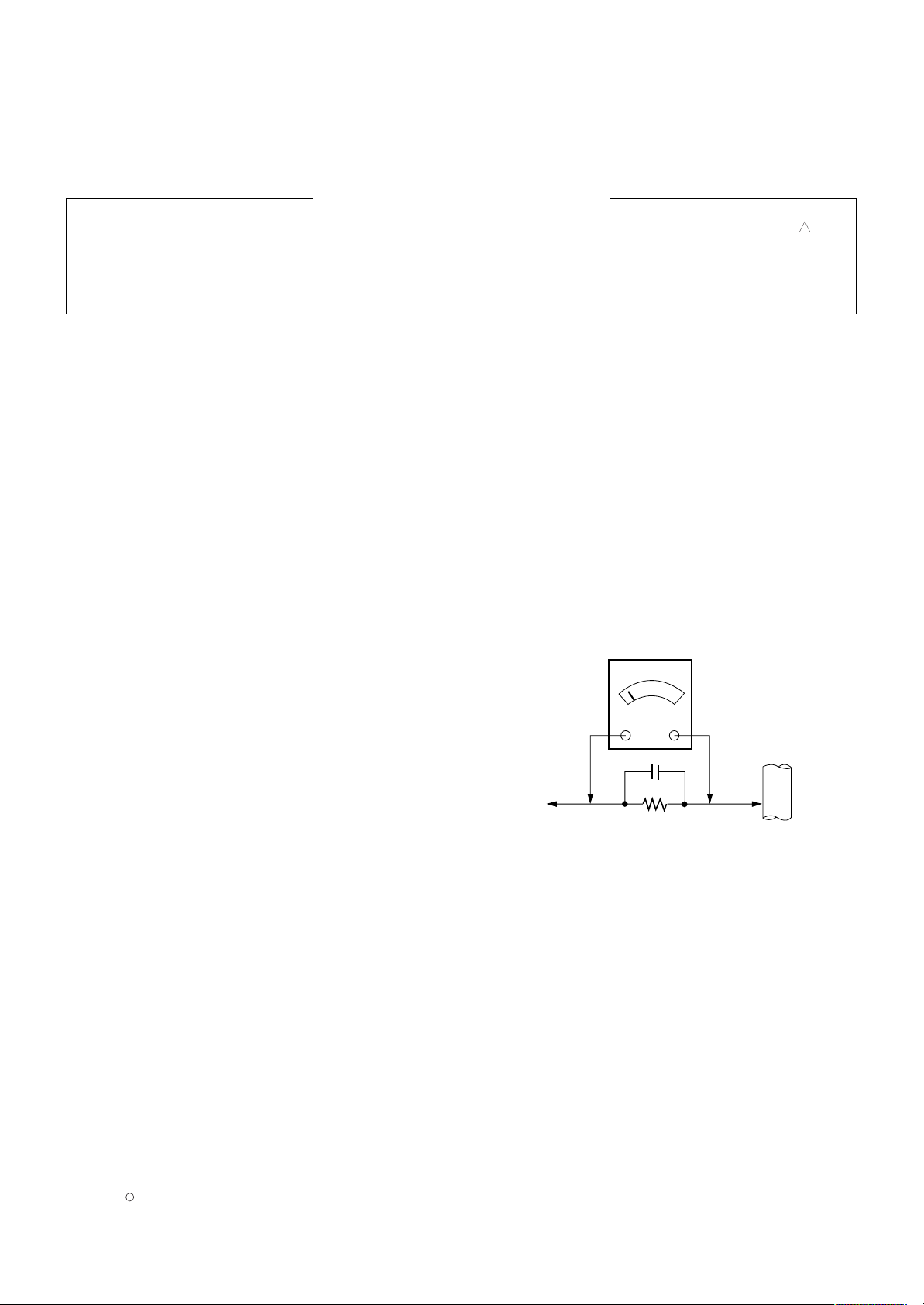
Leakage Current Hot Check (See below Figure)
Plug the AC cord directly into the AC outlet.
Do not use a line Isolation Transformer during this check.
Connect 1.5K/10watt resistor in parallel with a 0.15uF capacitor
between a known good earth ground (Water Pipe, Conduit, etc.)
and the exposed metallic parts.
Measure the AC voltage across the resistor using AC voltmeter
with 1000 ohms/volt or more sensitivity.
Reverse plug the AC cord into the AC outlet and repeat AC voltage
measurements for each exposed metallic part. Any voltage
measured must not exceed 0.75 volt RMS which is corresponds to
0.5mA.
In case any measurement is out of the limits specified, there is
possibility of shock hazard and the set must be checked and
repaired before it is returned to the customer.
Leakage Current Hot Check circuit
1.5 Kohm/10W
To Instrument's
exposed
METALLIC PARTS
Good Earth Ground
such as WATER PIPE,
CONDUIT etc.
AC Volt-meter
When 25A is impressed between Earth and 2nd Ground
for 1 second, Resistance must be less than 0.1
*Base on Adjustment standard
IMPORTANT SAFETY NOTICE
0.15uF
Ω

LGE Internal Use OnlyCopyright LG Electronics. Inc. All right reserved.
Only for training and service purposes
C
2009
- 4 -
CAUTION: Before servicing receivers covered by this service
manual and its supplements and addenda, read and follow the
SAFETY PRECAUTIONS on page 3 of this publication.
NOTE: If unforeseen circumstances create conflict between the
following servicing precautions and any of the safety precautions on
page 3 of this publication, always follow the safety precautions.
Remember: Safety First.
General Servicing Precautions
1. Always unplug the receiver AC power cord from the AC power
source before;
a. Removing or reinstalling any component, circuit board
module or any other receiver assembly.
b. Disconnecting or reconnecting any receiver electrical plug or
other electrical connection.
c. Connecting a test substitute in parallel with an electrolytic
capacitor in the receiver.
CAUTION: A wrong part substitution or incorrect polarity
installation of electrolytic capacitors may result in an
explosion hazard.
2. Test high voltage only by measuring it with an appropriate high
voltage meter or other voltage measuring device (DVM,
FETVOM, etc) equipped with a suitable high voltage probe.
Do not test high voltage by "drawing an arc".
3. Do not spray chemicals on or near this receiver or any of its
assemblies.
4. Unless specified otherwise in this service manual, clean
electrical contacts only by applying the following mixture to the
contacts with a pipe cleaner, cotton-tipped stick or comparable
non-abrasive applicator; 10% (by volume) Acetone and 90% (by
volume) isopropyl alcohol (90%-99% strength)
CAUTION: This is a flammable mixture.
Unless specified otherwise in this service manual, lubrication of
contacts in not required.
5. Do not defeat any plug/socket B+ voltage interlocks with which
receivers covered by this service manual might be equipped.
6. Do not apply AC power to this instrument and/or any of its
electrical assemblies unless all solid-state device heat sinks are
correctly installed.
7. Always connect the test receiver ground lead to the receiver
chassis ground before connecting the test receiver positive
lead.
Always remove the test receiver ground lead last.
8. Use with this receiver only the test fixtures specified in this
service manual.
CAUTION: Do not connect the test fixture ground strap to any
heat sink in this receiver.
Electrostatically Sensitive (ES) Devices
Some semiconductor (solid-state) devices can be damaged easily
by static electricity. Such components commonly are called
Electrostatically Sensitive (ES) Devices. Examples of typical ES
devices are integrated circuits and some field-effect transistors and
semiconductor "chip" components. The following techniques
should be used to help reduce the incidence of component
damage caused by static by static electricity.
1. Immediately before handling any semiconductor component or
semiconductor-equipped assembly, drain off any electrostatic
charge on your body by touching a known earth ground.
Alternatively, obtain and wear a commercially available
discharging wrist strap device, which should be removed to
prevent potential shock reasons prior to applying power to the
unit under test.
2. After removing an electrical assembly equipped with ES
devices, place the assembly on a conductive surface such as
aluminum foil, to prevent electrostatic charge buildup or
exposure of the assembly.
3. Use only a grounded-tip soldering iron to solder or unsolder ES
devices.
4. Use only an anti-static type solder removal device. Some solder
removal devices not classified as "anti-static" can generate
electrical charges sufficient to damage ES devices.
5. Do not use freon-propelled chemicals. These can generate
electrical charges sufficient to damage ES devices.
6. Do not remove a replacement ES device from its protective
package until immediately before you are ready to install it.
(Most replacement ES devices are packaged with leads
electrically shorted together by conductive foam, aluminum foil
or comparable conductive material).
7. Immediately before removing the protective material from the
leads of a replacement ES device, touch the protective material
to the chassis or circuit assembly into which the device will be
installed.
CAUTION: Be sure no power is applied to the chassis or circuit,
and observe all other safety precautions.
8. Minimize bodily motions when handling unpackaged
replacement ES devices. (Otherwise harmless motion such as
the brushing together of your clothes fabric or the lifting of your
foot from a carpeted floor can generate static electricity
sufficient to damage an ES device.)
General Soldering Guidelines
1. Use a grounded-tip, low-wattage soldering iron and appropriate
tip size and shape that will maintain tip temperature within the
range or 500
°F to 600°F.
2. Use an appropriate gauge of RMA resin-core solder composed
of 60 parts tin/40 parts lead.
3. Keep the soldering iron tip clean and well tinned.
4. Thoroughly clean the surfaces to be soldered. Use a mall wirebristle (0.5 inch, or 1.25cm) brush with a metal handle.
Do not use freon-propelled spray-on cleaners.
5. Use the following unsoldering technique
a. Allow the soldering iron tip to reach normal temperature.
(500
°F to 600°F)
b. Heat the component lead until the solder melts.
c. Quickly draw the melted solder with an anti-static, suction-
type solder removal device or with solder braid.
CAUTION: Work quickly to avoid overheating the circuit
board printed foil.
6. Use the following soldering technique.
a. Allow the soldering iron tip to reach a normal temperature
(500
°F to 600°F)
b. First, hold the soldering iron tip and solder the strand against
the component lead until the solder melts.
c. Quickly move the soldering iron tip to the junction of the
component lead and the printed circuit foil, and hold it there
only until the solder flows onto and around both the
component lead and the foil.
CAUTION: Work quickly to avoid overheating the circuit
board printed foil.
d. Closely inspect the solder area and remove any excess or
splashed solder with a small wire-bristle brush.
SERVICING PRECAUTIONS

LGE Internal Use OnlyCopyright LG Electronics. Inc. All right reserved.
Only for training and service purposes
C
2009
- 5 -
IC Remove/Replacement
Some chassis circuit boards have slotted holes (oblong) through
which the IC leads are inserted and then bent flat against the
circuit foil. When holes are the slotted type, the following technique
should be used to remove and replace the IC. When working with
boards using the familiar round hole, use the standard technique
as outlined in paragraphs 5 and 6 above.
Removal
1. Desolder and straighten each IC lead in one operation by gently
prying up on the lead with the soldering iron tip as the solder
melts.
2. Draw away the melted solder with an anti-static suction-type
solder removal device (or with solder braid) before removing the
IC.
Replacement
1. Carefully insert the replacement IC in the circuit board.
2. Carefully bend each IC lead against the circuit foil pad and
solder it.
3. Clean the soldered areas with a small wire-bristle brush.
(It is not necessary to reapply acrylic coating to the areas).
"Small-Signal" Discrete Transistor
Removal/Replacement
1. Remove the defective transistor by clipping its leads as close as
possible to the component body.
2. Bend into a "U" shape the end of each of three leads remaining
on the circuit board.
3. Bend into a "U" shape the replacement transistor leads.
4. Connect the replacement transistor leads to the corresponding
leads extending from the circuit board and crimp the "U" with
long nose pliers to insure metal to metal contact then solder
each connection.
Power Output, Transistor Device
Removal/Replacement
1. Heat and remove all solder from around the transistor leads.
2. Remove the heat sink mounting screw (if so equipped).
3. Carefully remove the transistor from the heat sink of the circuit
board.
4. Insert new transistor in the circuit board.
5. Solder each transistor lead, and clip off excess lead.
6. Replace heat sink.
Diode Removal/Replacement
1. Remove defective diode by clipping its leads as close as
possible to diode body.
2. Bend the two remaining leads perpendicular y to the circuit
board.
3. Observing diode polarity, wrap each lead of the new diode
around the corresponding lead on the circuit board.
4. Securely crimp each connection and solder it.
5. Inspect (on the circuit board copper side) the solder joints of
the two "original" leads. If they are not shiny, reheat them and if
necessary, apply additional solder.
Fuse and Conventional Resistor
Removal/Replacement
1. Clip each fuse or resistor lead at top of the circuit board hollow
stake.
2. Securely crimp the leads of replacement component around
notch at stake top.
3. Solder the connections.
CAUTION: Maintain original spacing between the replaced
component and adjacent components and the circuit board to
prevent excessive component temperatures.
Circuit Board Foil Repair
Excessive heat applied to the copper foil of any printed circuit
board will weaken the adhesive that bonds the foil to the circuit
board causing the foil to separate from or "lift-off" the board. The
following guidelines and procedures should be followed whenever
this condition is encountered.
At IC Connections
To repair a defective copper pattern at IC connections use the
following procedure to install a jumper wire on the copper pattern
side of the circuit board. (Use this technique only on IC
connections).
1. Carefully remove the damaged copper pattern with a sharp
knife. (Remove only as much copper as absolutely necessary).
2. carefully scratch away the solder resist and acrylic coating (if
used) from the end of the remaining copper pattern.
3. Bend a small "U" in one end of a small gauge jumper wire and
carefully crimp it around the IC pin. Solder the IC connection.
4. Route the jumper wire along the path of the out-away copper
pattern and let it overlap the previously scraped end of the good
copper pattern. Solder the overlapped area and clip off any
excess jumper wire.
At Other Connections
Use the following technique to repair the defective copper pattern
at connections other than IC Pins. This technique involves the
installation of a jumper wire on the component side of the circuit
board.
1. Remove the defective copper pattern with a sharp knife.
Remove at least 1/4 inch of copper, to ensure that a hazardous
condition will not exist if the jumper wire opens.
2. Trace along the copper pattern from both sides of the pattern
break and locate the nearest component that is directly
connected to the affected copper pattern.
3. Connect insulated 20-gauge jumper wire from the lead of the
nearest component on one side of the pattern break to the lead
of the nearest component on the other side.
Carefully crimp and solder the connections.
CAUTION: Be sure the insulated jumper wire is dressed so the
it does not touch components or sharp edges.
LGE Internal Use OnlyCopyright LG Electronics. Inc. All right reserved.
Only for training and service purposes
C
2009
- 6 -
SPECIFICATION
NOTE : Specifications and others are subject to change without notice for improvement
.
4. Electrical specification
4.1 General Specification
1. Application range
This spec sheet is applied to LCD TV used LP91A/ B/ C/ D
chassis.
2. Specification
Each part is tested as below without special appointment.
1) Temperature : 25±5ºC (77±9ºF), CST : 40±5ºC
2) Relative Humidity : 65±10%
3)
Power Voltage : Standard input voltage(100~240V@50/60Hz)
* Standard Voltage of each products is marked by models.
4) Specification and performance of each parts are followed
each drawing and specification by part number in
accordance with BOM.
5) The receiver must be operated for about 5 minutes prior to
the adjustment.
3. Test method
1) Performance: LGE TV test method followed
2) Demanded other specification
- Safety: CE, IEC specification
- EMC : CE, IEC
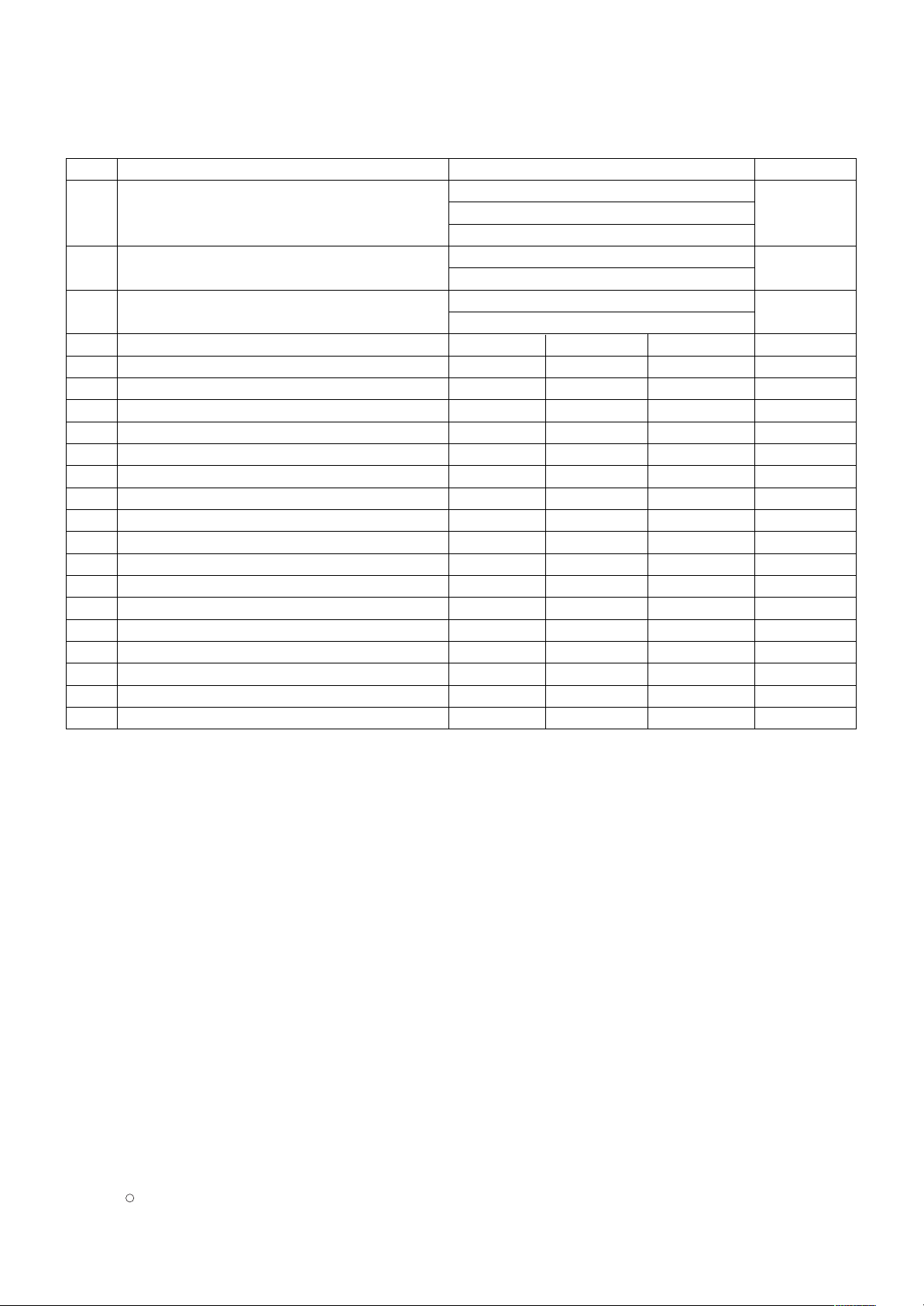
No Item Specification Remark
1 Display Screen 47” wide Color Display Module Resolution: 1366*768/1920* 1080
Device 55” wide Color Display Module Resolution: 1920* 1080
2 Aspect Ratio 16:9
3 LCD Module 47” TFT WUXGA LCD 1096 x 640 x 50/ (51) without inverter/ with inverter
55” TFT WUXGA LCD
4 Operating Environment Temp.: 0 ~ 40 deg
Humidity : 0 ~ 80 %
5 Storage Environment Temp.: -20 ~ 60 deg
Humidity : 0~ 85 %
6 Input Voltage AC100 ~ 240V,50/60Hz
7 ≤ 270 W 47”FHD
≤ 280 W 47”FHD,100Hz
≤ 360 W 55”FHD,100Hz
8 Coating 3H
LP91A 47LH30FR(FHD)
LP91B
47LH50YR(FHD+100Hz)
55LH50YR(FHD+100Hz)
LP91C 47LH90QR(FHD)
LP91D 47LH70YR(FHD+100Hz+Slim)
- 7 -
LGE Internal Use OnlyCopyright LG Electronics. Inc. All right reserved.
Only for training and service purposes
C
2009
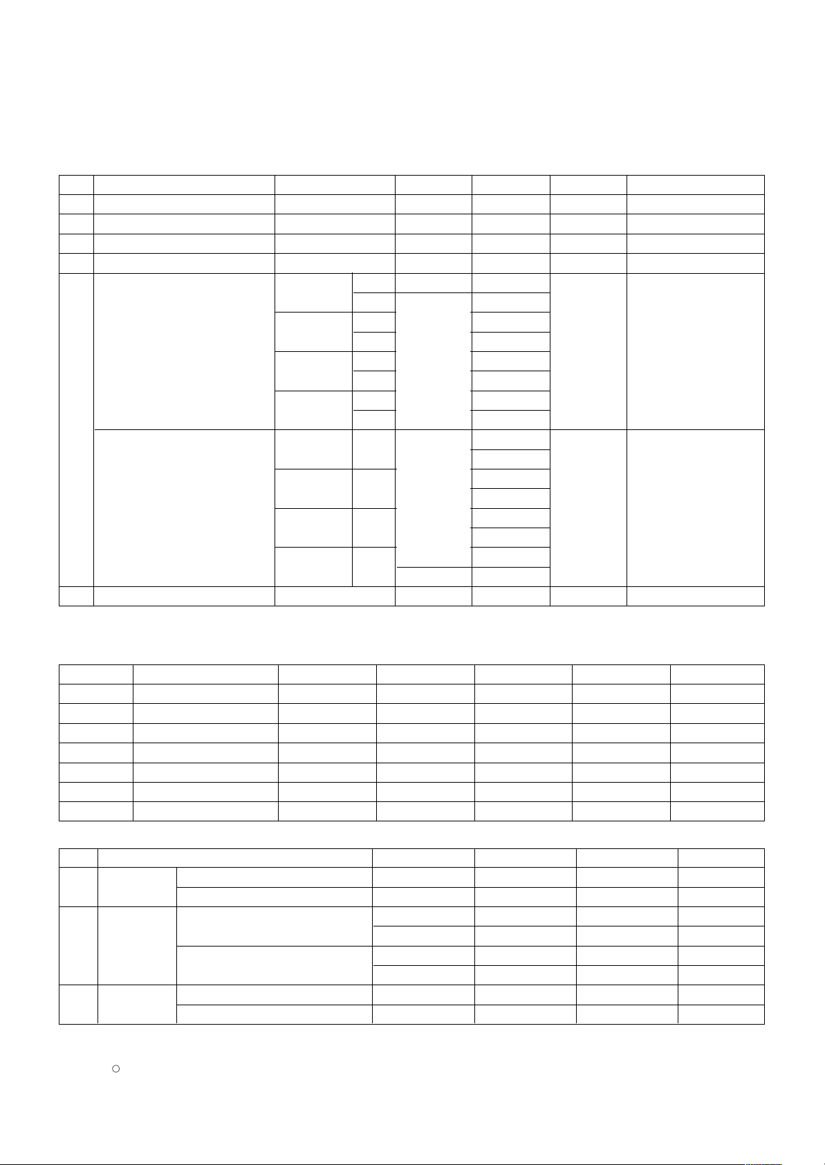
5 Safety and Regulation
No Item Min Typ Max Unit Remark
1. Incline Plane Tip Test 10 deg IEC60065
2. Isolation Gap,AC-AC 3.0 mm
3. Isolation Gap, Hot and Cold 6 mm
4. Isolation Gap,Primary <-> GND 3 mm
Isolation Gap,Primary <-> Secondary 6.0 mm
5. Power Consumption,Max 270 W 47” FHD
280 W 47” FHD+100Hz
360 W 55” FHD+100Hz
6. Power Consumption,Stand by 0.5 0.6 W
OFF mode: 1W under(china only)
7. Power Consumption,Switch off 0.1 W
8. Dielectric Voltage AC <-> FG 1.5 At 100mA for 1 sec(Line)
1.5 KV At 100mA for 1 min(OQC)
Without 3 At 100mA for 1 sec(Line)
3 KV At 100mA for 1 min(OQC)
9. Isolation Resistance 4 MΩ IEC60065
10. Leakage Current UL/CSA 0.5 mA rms
Etc. 0.35 V Peak
11. Flammability - Back Cover V0 UL94
12. CSA Compliance Safety CSA 60065
EMC GRR Part II
13. UL Compliance Safety UL6500
EMC FCC Part15 ClassA
FCC Part15 ClassB
14. IEC Compliance Safety IEC60065
EMC CISPR
15. CE Compliance Safety EN60065
EMC EN55013, EN55020
6. Power
No Item Min Typ Max Unit Remark
1. AC Power Shut Down Voltage,SET 90 264 Vac
2. DC Voltage,Module Logicvoltage(Vcc) 4.5 5.0 5.5
11.4 12.0 12.6 Vdc
3. DC Voltage,VSC 12Vcc 11.4 12 12.6 Vdc
4. DC Voltage,VSC St-By 4.94 5.2 5.46 Vdc
23.8 24 25.2 Vdc PSU
5. DC Voltage,Sound amp Vcc 19 20 21 Vdc LIPS
14.25 15 15.75 Vdc LIPS
6. DC Voltage,Tuner +B 4.8 5.0 5.2 Vdc
- 8 -
LGE Internal Use OnlyCopyright LG Electronics. Inc. All right reserved.
Only for training and service purposes
C
2009
7. Bluetooth
No Item Min Typ Max Unit
1 SIG Qualification Profile
Protocol
RF Test
2 Wireless test(R &TTE) Wireless RF : EN 300 328
Wireless EMC : 301 489
3 CE-EMC(TV &MNT) TV : EN 55013 /EN 55020
MNT : EN 550222 /EN55024
4 Bluetooth module voltage 3.0 3.3 3.6 Voltage
5 Operation Temperature range -40 85 C
6 Storage Temperature range -40 105 C
7 Output Power -6 4 dBm
8 Frequency Range 2.402 2.480 GHz
9 Impedance at Antenna 50 Ohm
10 Sensitivity level (single slot) -70 -82 dBm
11 Sensitivity level (multi slot) -70 -80 dBm
12 ∆F1 avg 145 175 kHz
13 ∆F2 max 115 kHz
14 ∆F2 avg /∆F1 avg 80 kHz
15 ICFT -75 75 kHz
16 Drift -25 25 kHz
17 Adjacent channel power(+-2Mhz) -20 dBm
18 Adjacent channel power(+-3Mhz) -40 dBm
19 Adjacent channel power(+-4Mhz) -40 dBm
20 Operation Distance 10 m
21 Operation Degree -45 0 45 Deg
- 9 -
LGE Internal Use OnlyCopyright LG Electronics. Inc. All right reserved.
Only for training and service purposes
C
2009
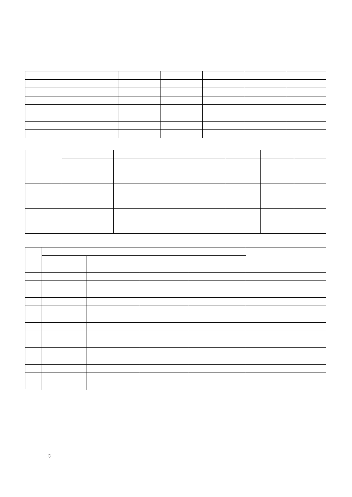
8. Chroma& Brightness (Optical)
8.1 LCD Module
the Color Coordinates check condition : Picture mode Vivid
No. Item Specification Min. Typ. Max. Remark
1. Luminance LGD 47” HD,FHD 400 500
cd/m
2
(W/O PC mode)
LGD 55” FHD
360 450
2. VIew angle (R/L, U/D) 178/ 178
LGD 55” only 176/ 176
Wx Typ 0.270/0.279 Typ
White
Wy -0.03 0.292 +0.03
3. Color Coordinates Xr 0.638/0.640 LGD 47” (HD/FHD)
RED
Yr 0.342/0.335
Xg 0.296/0.289
Green
Yg 0.615/0.610
Xb 0.144
Blue
Yb 0.064/0.066
Wx Typ 0.272 Typ
White
Wy -0.03 0.277 +0.03 LGD 55” (100Hz)
Xr 0.640
RED
Yr 0.330
Xg 0.280
Green
Yg 0.600
Xb 0.150
Blue
Yb 0.060
4. Luminance Variation 1.3
8.2 Chroma ( SET condition )
** The W/B Tolerance is ±0.015 for Adjustment (W/
To check the Coordinates of White Balance, you have to measure at the below conditions.
(If you miss the upper condition, the coordinates of W/B can be lower than the spec.)
Input mode Signal Picture Mode Dynamic Contrast Dynamic Color Black Level OPC
RF NTSC-M Vivid Off Off Low Off
PAL-BG Vivid Off Off NA Off
AV NTSC-J Vivid Off Off High Off
PAL-BG Vivid Off Off NA Off
Component 720P Vivid Off Off High Off
RGB 1024x768 Vivid Off NA NA Off
HDMI DTV 720P(16~235) Vivid Off Off Low Off
No Item Min Typ Max Remark
1. Cool White Balance,X axis 0.274 0.276 0.278
White Balance,Y axis 0.281 0.283 0.285
2. Medium White Balance,X axis 0.283 0.285 0.287
0.291 0.293 0.295
White Balance,Y axis 0.293 0.295 0.297
0.303 0.305 0.307
3. Warm White Balance,X axis 0.311 0.313 0.315
White Balance,Y axis 0.327 0.329 0.331
- 10 -
LGE Internal Use OnlyCopyright LG Electronics. Inc. All right reserved.
Only for training and service purposes
C
2009
9. Component Video Input (Y, P
B
, PR)
No
Specification
Remark
Resolution H-freq(kHz) V-freq(Hz) Pixel Clock(MHz)
1 720* 480 15.73 59.94 13.500 SDTV, DVD 480I( 525I)
2 720* 480 15.75 60.00 13.514 SDTV, DVD 480I( 525I)
3 720* 576 15.625 50.00 13.500 SDTV, DVD 576I( 625I) 50Hz
4 720* 480 31.47 59.94 27.000 SDTV 480P
5 720* 480 31.50 60.00 27.027 SDTV 480P
6 720* 576 31.25 50.00 27.000 SDTV 576P 50Hz
7 1280* 720 44.96 59.94 74.176 HDTV 720P
8 1280* 720 45.00 60.00 74.250 HDTV 720P
9 1280* 720 37.50 50.00 74.25 HDTV 720P 50Hz
10 1920* 1080 28.125 50.00 74.250 HDTV 1080I 50Hz,
11 1920* 1080 33.72 59.94 74.176 HDTV 1080I
12 1920* 1080 33.75 60.00 74.25 HDTV 1080I
13 1920* 1080 56.25 50 148.5 HDTV 1080P
14 1920* 1080 67.432 59.94 148.350 HDTV 1080P
15 1920* 1080 67.5 60.00 148.5 HDTV 1080P
8.3 Set Optical Feature
8.3.1 General feature
- Measurement Condition: Full white/Vivid ->Measure the black luminance after 30 seconds.
Input mode Signal Picture Mode Dynamic Contrast Dynamic Color Black Level OPC
RF NTSC-M Vivid High High Low Off
PAL-BG Vivid High High NA Off
AV NTSC-J Vivid High High High Off
PAL-BG Vivid High High NA Off
Component 720P Vivid High High High Off
RGB 1024x768 Vivid High NA NA Off
HDMI DTV 720P(16~235) Vivid High High Low Off
- C/ R is excepted for RF/ PC mode
47”( FHD) Contrast Ratio Dynamic CR 40000: 1 50000: 1
L WH (RF) 300 450
Surface L WH (AV,Component,HDMI) 360 450
Luminance,white L WH (PC) 250 Cd/ m 2
47 inch Contrast Ratio Dynamic CR 65000: 1 80000: 1
(FHD+ 100Hz) Surface L WH (RF/ AV/ Component/ HDMI) 360 450 Cd/ m 2
Luminance,white L WH (PC) 250 Cd/ m 2
55Inch Contrast Ratio Dynamic CR 65000: 1 80000: 1
(FHD+ 100Hz) Surface L WH (RF/ AV/ Component/ HDMI) 320 400 Cd/ m 2
Luminance,white L WH (PC) 250 Cd/ m 2
 Loading...